CYT2B6 TRAVEO™ T2G 32-bit Automotive MCU
Based on Arm®
Cortex®-M4F single
Datasheet
General description
Infineon's TRAVEO™ T2G 32-bit Automotive MCU is a high-performance, low-power controller designed for automotive applications, compliant to ISO 26262 for functional safety and ISO 21434 for cybersecurity. CYT2B6 is a family of TRAVEO™ T2G microcontrollers targeted at automotive systems such as body control units. CYT2B6 has an Arm® Cortex®-M4F CPU for primary processing, and an Arm® Cortex®-M0+ CPU for peripheral and security processing. These devices contain embedded peripherals supporting Controller Area Network with Flexible Data rate (CAN FD), and Local Interconnect Network (LIN). TRAVEO™ T2G devices are manufactured on an advanced 40-nm process. CYT2B6 incorporates a low-power flash memory, multiple high-performance analog and digital peripherals, and enables the creation of a secure computing platform.
Features
Dual CPU subsystem
80-MHz (max) 32-bit Arm® Cortex®-M4F CPU with
Single-cycle multiply
Single-precision floating point unit (FPU)
Memory protection unit (MPU)
80-MHz (max) 32-bit Arm® Cortex®-M0+ CPU with
Single-cycle multiply
Memory protection unit
Inter-processor communication in hardware
Three DMA controllers
Peripheral DMA controller #0 (P-DMA0) with 54 channels
Peripheral DMA controller #1 (P-DMA1) with 26 channels
Memory DMA controller #0 (M-DMA0) with 2 channels
Integrated memories
576 KB of code-flash with an additional 64 KB of work-flash
Read-While-Write (RWW) allows updating the code-flash/work-flash while executing from it
Single- and dual-bank modes (specifically for Firmware update Over The Air [FOTA])
Flash programming through SWD/JTAG interface
64 KB of SRAM with selectable retention granularity
- ISO 21434 compliant / EVITA Full1
Supports enhanced Secure Hardware Extension (eSHE) and Hardware Security Module (HSM)
Secure boot and authentication
Using digital signature verification
Using fast secure boot
AES: 128-bit blocks, 128-/192-/256-bit keys
3DES: 64-bit blocks, 64-bit key
Vector unit 2 supporting asymmetric key cryptography such as Rivest-Shamir-Adleman (RSA) and Elliptic Curve (ECC)
SHA-1/2/3 2 : SHA-512, SHA-256, SHA-160 with variable length input data
CRC 2 : supports CCITT CRC16 and IEEE-802.3 CRC32
True random number generator (TRNG) and pseudo random number generator (PRNG)
Galois/Counter Mode (GCM)
ISO 26262 functional safety compliant for ASIL-B
Memory protection unit (MPU)
Shared memory protection unit (SMPU)
Peripheral protection unit (PPU)
Watchdog timer (WDT)
Multi-counter watchdog timer (MCWDT)
Low-voltage detector (LVD)
Brown-out detector (BOD)
Overvoltage detection (OVD)
Clock supervisor (CSV)
Hardware error correction (SECDED ECC) on all safety-critical memories (SRAM, flash)
Low-power 2.7 V to 5.5 V operation
Low-power Active, Sleep, Low-power Sleep, DeepSleep, and Hibernate modes for fine-grained power management
Configurable options for robust BOD
Two threshold levels (2.7 V and 3.0 V) for BOD on V DDD and V DDA
One threshold level (1.1 V) for BOD on V CCD
Wakeup support
A GPIO pin to wakeup from Hibernate mode
Up to 78 GPIO pins to wakeup from Sleep modes
Event Generator, SCB, Watchdog Timer, RTC alarms to wake from DeepSleep modes
Clock sources
Internal main oscillator (IMO)
Internal low-speed oscillator (ILO)
External crystal oscillator (ECO)
Watch crystal oscillator (WCO)
Phase-locked loop (PLL)
Frequency-locked loop (FLL)
Communication interfaces
Up to four CAN FD channels
Increased data rate (up to 8 Mbps) compared to classic CAN, limited by physical layer topology and transceivers
Compliant to ISO 11898-1:2015
Supports all the requirements of Bosch CAN FD Specification V1.0 for non-ISO CAN FD
ISO 16845:2015 certificate available
Up to six runtime-reconfigurable SCB (serial communication block) channels, each configurable as I 2 C, SPI, or UART
Up to five independent LIN channels
LIN protocol compliant with ISO 17987
Timers
Up to 50 16-bit and two 32-bit timer/counter pulse-width modulator (TCPWM) blocks
Up to four 16-bit counters for motor control
Up to 46 16-bit counters and two 32-bit counters for regular operations
Supports timer, capture, quadrature decoding, pulse-width modulation (PWM), PWM with dead time (PWM_DT), pseudo-random PWM (PWM_PR), and shift-register (SR) modes
Up to 11 Event Generation (EVTGEN) timers supporting cyclic wakeup from DeepSleep
Events trigger a specific device operation (such as execution of an interrupt handler, a SAR ADC conversion, and so on)
Real time clock (RTC)
Year/Month/Date, Day-of-week, Hour:Minute:Second fields
12- and 24-hour formats
Automatic leap-year correction
I/O
Up to 78 programmable I/Os
Two I/O types
GPIO Standard (GPIO_STD)
GPIO Enhanced (GPIO_ENH)
Regulators
Generates 1.1-V nominal core supply from a 2.7-V to 5.5-V input supply
Two types of regulators
DeepSleep
Core internal
Programmable analog
Three SAR A/D converters with up to 35 external channels (32 I/Os + 3 I/Os for motor control)
ADC0 supports 11 logical channels, with 11 + 1 physical connections
ADC1 supports 13 logical channels, with 13 + 1 physical connections
ADC2 supports 8 logical channels, with 8 + 1 physical connections
Any external channel can be connected to any logical channel in the respective SAR
Each ADC supports 12-bit resolution and sampling rates of up to 1 Msps
Each ADC also supports up to six internal analog inputs like
Bandgap reference to establish absolute voltage levels
Calibrated diode for junction temperature calculations
Two AMUXBUS inputs and two direct connections to monitor supply levels
Each ADC supports addressing of external multiplexers
Each ADC has a sequencer supporting autonomous scanning of configured channels
Synchronized sampling of all ADCs for motor-sense applications
Smart I/O
Up to three Smart I/O blocks, which can perform Boolean operations on signals going to and from I/Os
Up to 16 I/Os (GPIO_STD) supported
Debug interface
JTAG controller and interface compliant to IEEE-1149.1-2001
Arm® SWD (serial wire debug) port
Supports Arm® Embedded Trace Macrocell (ETM) Trace
Data trace using SWD
Instruction and data trace using JTAG
Compatible with industry-standard tools
GHS/MULTI or IAR EWARM for code development and debugging
Packages
64-LQFP, 10 × 10 × 1.7 mm (max), 0.5-mm lead pitch
80-LQFP, 12 × 12 × 1.7 mm (max). 0.5-mm lead pitch
100-LQFP, 14 × 14 × 1.7 mm (max), 0.5-mm lead pitch
Certification
Qualified for automotive application according to AEC-Q100
Features list
Features | Packages | ||
|---|---|---|---|
64-LQFP | 80-LQFP | 100-LQFP | |
CPU | |||
Core | 32-bit Arm® Cortex®-M4F CPU and 32-bit Arm® Cortex®-M0+ CPU | ||
Functional safety | ISO 26262 ASIL-B compliant | ||
Operating voltage | 2.7 V to 5.5 V | ||
Core voltage | 1.05 V to 1.15 V | ||
Operating frequency | Arm® Cortex®-M4F 80 MHz (max) and Arm® Cortex®-M0+ 80 MHz (max), related by integer frequency ratio (that is, 1:1, 1:2, 1:3, and so on) | ||
MPU, PPU | Supported | ||
FPU | Single precision (32-bit) | ||
DSP-MUL/DIV/MAC | Supported by Arm® Cortex®-M4F CPU | ||
Memory | |||
Code-flash | 576 KB (448 KB + 128 KB) | ||
Work-flash | 64 KB (48 KB + 16 KB) | ||
SRAM (configurable for retention) | 64 KB | ||
ROM | 32 KB | ||
Communication interfaces | |||
CAN0 (CAN FD: Up to 8 Mbps) | 2 ch | ||
CAN1 (CAN FD: Up to 8 Mbps) | 1 ch | 2 ch | |
CAN RAM | 24 KB per instance (2 ch), 48 KB in total | ||
Serial communication block (SCB/UART) | 6 ch | ||
Serial communication block (SCB/I 2 C) | 5 ch | 6 ch | |
Serial communication block (SCB/SPI) | 3 ch | 6 ch | |
LIN0 | 5 ch | ||
Timers | |||
RTC | 1 ch | ||
TCPWM (16-bit) (Motor Control) | 4 ch | ||
TCPWM (16-bit) | 46 ch | ||
TCPWM (32-bit) | 2 ch | ||
External interrupts | 49 | 63 | 78 |
Analog | |||
12-bit, 1 Msps SAR ADC | 3 units (SAR0/11, SAR1/13, SAR2/8 logical channels) 3 | ||
22 external channels (SAR0 8 ch, SAR1 7 ch, SAR2 7 ch) | 28 external channels (SAR0 10 ch, SAR1 10 ch, SAR2 8 ch) | 32 external channels (SAR0 11 ch, SAR1 13 ch, SAR2 8 ch) | |
18 ch (6 per ADC) Internal sampling | |||
Motor control input | 3 ch (synchronous sampling of one channel on each of the 3 ADCs) | ||
ISO 21434 compliant | |||
Flash security (program/work read
protection) | Supported | ||
Flash chip erase enable | Configurable | ||
eSHE | By separate firmware 4 | ||
System | |||
DMA controller | P-DMA0 with 54 channels (16 general purpose), P-DMA1 with 26 channels (8 general purpose), and M-DMA0 with 2 channels | ||
Internal main oscillator | 8 MHz | ||
Internal low-speed oscillator | 32.768 kHz (nominal) | ||
PLL | Input frequency: 3.988 to 33.34 MHz, PLL output frequency: up to 80 MHz | ||
FLL | Input frequency: 0.25 to 80 MHz, FLL output frequency: up to 80 MHz | ||
Watchdog timer and multi-counter watchdog
timer | Supported (WDT + 2× MCWDT) MCWDT#0 tied to CM0+, MCWDT#1 to CM4 | ||
Clock supervisor | Supported | ||
Cyclic wakeup from DeepSleep | Supported | ||
GPIO_STD | 45 | 59 | 74 |
GPIO_ENH | 4 | ||
Smart I/O (Blocks) | 3 blocks, 9 I/Os | 3 blocks, 14 I/Os | 3 blocks, 16 I/Os |
Low-voltage detect | Two, 26 selectable levels | ||
Maximum ambient temperature | 105°C for S-grade and 125°C for E-grade | ||
Debug interface | SWD/JTAG | ||
Debug trace | Arm® Cortex®-M4F ETB size of 8 KB, Arm® Cortex®-M0+ MTB size of 4 KB | ||
Communication peripheral instance list
The following table lists the instances supported under each package for communication peripherals, based on the minimum pins needed for the functionality.
Module | 64-LQFP | 80-LQFP | 100-LQFP | Minimum pin functions |
|---|---|---|---|---|
CAN0 | 0/1 | 0/1 | 0/1 | TX, RX |
CAN1 | 0 | 0/1 | 0/1 | TX, RX |
LIN0 | 0/1/2/3/4 | 0/1/2/3/4 | 0/1/2/3/4 | TX, RX |
SCB/UART | 0/1/3/4/5/7 | 0/1/3/4/5/7 | 0/1/3/4/5/7 | TX, RX |
SCB/I 2 C | 0/3/4/5/7 | 0/1/3/4/5/7 | 0/1/3/4/5/7 | SCL, SDA |
SCB/SPI | 0/3/4 | 0/1/3/4/5/7 | 0/1/3/4/5/7 | MISO, MOSI, SCK, SELECT0 |
Blocks and functionality
Block diagram
Figure 1.
Block diagram
The Figure 1 shows the CYT2B6 architecture, giving a simplified view of the interconnection between subsystems and blocks. CYT2B6 has four major subsystems: CPU, system resources, peripherals, and I/O 5 , 6 . The color-coding shows the lowest power mode where the particular block is still functional.
CYT2B6 provides extensive support for programming, testing, debugging, and tracing of both hardware and firmware.
Debug-on-chip functionality enables in-system debugging using the production device. It does not require special interfaces, debugging pods, simulators, or emulators.
The JTAG interface is fully compatible with industry-standard third-party probes such as I-jet, J-Link, and GHS.
The debug circuits are enabled by default.
CYT2B6 provides a high level of security with robust flash protection and the ability to disable features such as debug.
Additionally, each device interface can be permanently disabled for applications concerned with phishing attacks from a maliciously reprogrammed device or attempts to defeat security by starting and interrupting flash programming sequences. All programming, debug, and test interfaces are disabled when maximum device security is enabled.
Functional description
CPU subsystem
CPU
The CYT2B6 CPU subsystem contains a 32-bit Arm® Cortex®-M0+ CPU with MPU and a 32-bit Arm® Cortex®-M4F CPU with MPU, and single-precision FPU. This subsystem also includes P-/M-DMA controllers, a cryptographic accelerator, 576 KB of code-flash, 64 KB of work-flash, 64 KB of SRAM, and 32 KB of ROM.
The Cortex®-M0+ CPU provides a secure, un-interruptible boot function. This guarantees that, following completion of the boot function, system integrity is valid and privileges are enforced. Shared resources (flash, SRAM, peripherals, and so on) can be accessed through bus arbitration, and exclusive accesses are supported by an inter-processor communication (IPC) mechanism using hardware semaphores.
DMA controllers
CYT2B6 has three DMA controllers: P-DMA0 with 16 general-purpose and 38 dedicated channels, P-DMA1 with 8 general-purpose and 18 dedicated channels, and M-DMA0 with two channels. P-DMA is used for peripheral-to-memory and memory-to-peripheral data transfers and provides low latency for a large number of channels. Each P-DMA controller uses a single data-transfer engine that is shared by the associated channels. General-purpose channels have a rich interconnect matrix including P-DMA cross triggering, which enables demanding data-transfer scenarios. Dedicated channels have a single triggering input (such as an ADC channel) to handle common transfer needs. M-DMA is used for memory-to-memory data transfers and provides high memory bandwidth for a small number of channels. M-DMA uses a dedicated data-transfer engine for each channel. They support independent accesses to peripherals using the AHB multi-layer bus.
Flash
CYT2B6 has 576 KB (448 KB with a 32-KB sector size, and 128 KB with an 8-KB sector size) of code-flash with an additional work-flash of up to 64 KB (48 KB with 2-KB sector size, and 16 KB with 128-B sectors size). Work-flash is optimized for reprogramming many more times than code-flash. Code-flash supports Read-While-Write (RWW) operation allowing flash to be updated while the CPU is active. Both the code-flash and work-flash areas support dual-bank operation for over-the-air (OTA) programming.
SRAM
CYT2B6 has 64 KB of SRAM. The SRAM0 controller provides DeepSleep retention in 32-KB increments.
ROM
CYT2B6 has 32-KB ROM that contains boot and configuration routines. This ROM enables secure boot and authentication of user flash to guarantee a secure system.
Cryptography accelerator for security
The cryptography accelerator implements (3)DES block cipher, AES block cipher, SHA hash, cyclic redundancy check, pseudo random number generation, true random number generation, galois/counter mode, and a vector unit to support asymmetric key cryptography such as RSA and ECC.
Depending on the part number, this block is either completely or partially available or not available at all. See Ordering information for more details.
System resources
Power system
The power system ensures that the supply voltage levels meet the requirements of each power mode, and provides a full-system reset when these levels are not valid. Internal power-on reset (POR) guarantees full-chip reset during the initial power ramp.
Three BOD circuits monitor the external supply voltages (V DDD , V DDA , V CCD ). The BOD on V DDD and V CCD are initially enabled and cannot be disabled. The BOD on V DDA is initially disabled and can be enabled by the user. For the external supplies V DDD and V DDA , BOD circuits are software configurable with two settings; a 2.7-V minimum voltage that is robust for all internal signaling and a 3.0-V minimum voltage, which is also robust for all I/O specifications (which are guaranteed at 2.7 V). The BOD on V CCD is provided as a safety measure and is not a robust detector.
Three overvoltage detection (OVD) circuits are provided for monitoring external supplies (V DDD , V DDA , V CCD ), and overcurrent detection circuits (OCD) for monitoring internal and external regulators. OVD thresholds on V DDD and V DDA are configurable with two settings; a 5.0-V and 5.5-V maximum voltage. Two voltage-detection circuits are provided to monitor the external supply voltage (V DDD ) for falling and rising levels, each configurable for one of the 26 selectable levels.
All BOD, OVD, and OCD circuits on V DDD and V CCD generate a reset, because these protect the CPUs and fault logic. The BOD and OVD circuits on V DDA can be configured to generate either a reset or a fault.
Regulators
CYT2B6 contains two regulators that provide power to the low-voltage core transistors: DeepSleep and core internal. These regulators accept a 2.7–5.5-V V DDD supply and provide a low-noise 1.1-V supply to various parts of the device. These regulators are automatically enabled and disabled by hardware and firmware when switching between power modes. The core internal and core external regulators operate in active mode, and provide power to the CPU subsystem and associated peripherals.
DeepSleep
The DeepSleep regulator is used to maintain power to a small number of blocks when in DeepSleep mode. These blocks include the ILO and WDT timers, BOD detector, SCB0, SRAM memories, Smart I/O, and other configuration memories. The DeepSleep regulator is enabled when in DeepSleep mode, and the core internal regulator is disabled. It is disabled when XRES_L is asserted (LOW) and when the core internal regulator is disabled.
Core internal
The core internal regulator supports load currents up to 150 mA, and is operational during device start-up (boot process), and in Active/Sleep modes.
Clock system
The CYT2B6 clock system provides clocks to all subsystems that require them, and glitch-free switching between different clock sources. In addition, the clock system ensures that no metastable conditions occur.
The clock system for CYT2B6 consists of the 8-MHz IMO, two ILOs, three watchdog timers, a PLL, an FLL, five clock supervisors (CSV), a 3.988- to 33.34 MHz ECO, and a 32.768-kHz WCO.
The clock system supports two main clock domains: CLK_HF, and CLK_LF.
CLK_HFx are the Active mode clocks. Each can use any of the high-frequency clock sources including IMO, EXT_CLK, ECO, FLL, or PLL
CLK_LF is a DeepSleep domain clock and provides a reference clock for the MCWDT or RTC modules. The reference clock for the CLK_LF domain is either disabled or selectable from ILO0, ILO1, or WCO
Name | Description |
CLK_HF0 | CPUSS clocks, PERI, and AHB infrastructure |
CLK_HF1 | Event Generator, also available in HSIOM as an output |
IMO clock source
The IMO is the frequency reference in CYT2B6 when no external reference is available or enabled. The IMO operates at a frequency of around 8 MHz.
ILO clock source
An ILO is a low-power oscillator, nominally 32.768 kHz, which generates clocks for a watchdog timer when in DeepSleep mode. There are two ILOs to ensure clock supervisor (CSV) capability in DeepSleep mode. ILO-driven counters can be calibrated to the IMO, WCO, or ECO to improve their accuracy. ILO1 is also used for clock supervision.
PLL and FLL
A PLL or FLL may be used to generate high-speed clocks from the IMO, the ECO, or EXT_CLK. The FLL provides a much faster lock than the PLL (5 µs instead of 35 µs) in exchange for a small amount of frequency error 7 .
Clock supervisor (CSV)
Each CSV allows one clock (reference) to supervise the behavior of another clock (monitored). Each CSV has counters for both the monitored and reference clocks. Parameters for each counter determine the frequency of the reference clock as well as the upper and lower frequency limits of the monitored clock. If the frequency range comparator detects a stopped clock or a clock outside the specified frequency range, an abnormal state is signaled and either a reset or an interrupt is generated.
EXT_CLK
One of the two GPIO_STD I/Os can be used to provide an external clock input of up to 80 MHz. This clock can be used as the source clock for either the PLL or FLL, or can be used directly by the CLK_HF domain.
ECO
The ECO provides high-frequency clocking using an external crystal connected to the ECO_IN and ECO_OUT pins. It supports fundamental mode (non-overtone) quartz crystals, in the range of 3.988 to 33.34 MHz. When used in conjunction with the PLL, it generates CPU and peripheral clocks up to device’s maximum frequency. ECO accuracy depends on the selected crystal. If the ECO is disabled, the associated pins can be used for any of the available I/O functions.
WCO
The WCO is a low-power, watch-crystal oscillator intended for real-time-clock applications. It requires an external 32.768-kHz crystal connected to the WCO_IN and WCO_OUT pins. The WCO can also be configured as a clock reference for CLK_LF, which is the clock source for the MCWDT and RTC.
Reset
CYT2B6 can be reset from a variety of sources, including software. Reset events are asynchronous and guarantee reversion to a known state. The reset cause (POR, BOD, OVD, overcurrent, XRES_L, WDT, MCWDT, software reset, fault, CSV, Hibernate wakeup, debug) is recorded in a register, which is sticky through reset and allows software to determine the cause of the reset. An XRES_L pin is available for external reset.
Watchdog timers
CYT2B6 has one watchdog timer (WDT) and two multi-counter watchdog timers (MCWDT).
The WDT is a free-running counter clocked only by ILO0, which allows it to be used as a wakeup source from Hibernate. Watchdog operation is possible during all power modes. To prevent a device reset from a WDT timeout, the WDT must be serviced during a configured window. A watchdog reset is recorded in the reset cause register.
An MCWDT is available for each of the CPU cores. These timers provide more capabilities than the WDT, and are only available in Active, Sleep, and DeepSleep modes. These timers have multiple counters that can be used separately or cascaded to trigger interrupts and/or resets. They are clocked from ILO0 or the WCO.
Power modes
CYT2B6 has the following power modes:
Active – all peripherals are available
Low-Power Active (LPACTIVE) – Low-power profile of Active mode where all peripherals and the CPUs are available, but with limited capability
Sleep – all peripherals except the CPUs are available
Low-Power Sleep (LPSLEEP) – Low-power profile of Sleep mode where all peripherals except the CPUs are available, but with limited capability
DeepSleep – only peripherals which work with CLK_LF are available
Hibernate – the device and I/O states are frozen, and the device resets on wakeup
Peripherals
Peripheral clock dividers
Integer and fractional clock dividers are provided for peripheral and timing purposes.
Divider | Count | Description |
|---|---|---|
div_8 | 32 | Integer divider, 8 bits |
div_16 | 16 | Integer divider, 16 bits |
div_24_5 | 8 | Fractional divider, 24.5 bits (24 integer bits, 5 fractional bits) |
Peripheral protection unit
The Peripheral Protection Unit (PPU) controls and monitors unauthorized access from all masters (CPU, P-/M-DMA, Crypto, and any enabled debug interface) to the peripherals. It allows or restricts data transfers on the bus infrastructure. The access rules are enforced based on specific properties of a transfer, such as an address range for the transfer and access attributes (such as read/write, user/privilege, and secure/non-secure).
12-bit SAR ADC
CYT2B6 contains three 1-Msps SAR ADCs. These ADCs can be clocked at up to 26.67 MHz and provide a 12-bit result in 26 clock cycles.
The references for all three SAR ADCs come from a dedicated pair of inputs: VREFH and VREFL 8 .
CYT2B6 devices support up to 53 logical ADC channels, and external inputs from up to 35 I/Os. Each ADC also supports six internal connections for diagnostic and monitoring purposes. The number of ADC channels (per ADC and package type) are listed in Table 1 .
Each ADC has a sequencer, which autonomously cycles through the configured channels (sequencer scan) with zero-switching overhead (that is, the aggregate sampling bandwidth, when clocked at 26.67 MHz, is equal to 1 Msps whether it is for a single channel or distributed over several channels). The sequencer switching is controlled through a state machine or firmware. The sequencer prioritizes trigger requests, enables the appropriate analog channel, controls ADC sampling, initiates ADC data conversion, manages results, and initiates subsequent conversions for repetitive or group conversions without CPU intervention.
Each SAR ADC has an analog multiplexer used to connect the signals to be measured to the ADC. It has 32 GPIO_STD inputs, one special GPIO_STD input for motor-sense, and six additional inputs to measure internal signals such as a band-gap reference, a temperature sensor, and power supplies. The device supports synchronous sampling of one motor-sense channel on each of the three ADCs.
CYT2B6 has one temperature sensor that is shared by all three ADCs. The temperature sensor must only be sampled by one ADC at a time. Software post processing is required to convert the temperature sensor reading into kelvin or Celsius values.
To accommodate signals with varying source impedances and frequencies, it is possible to have different sample times programmed for each channel. Each ADC also supports range comparison, which allows fast detection of out-of-range values without having to wait for a sequencer scan to complete and for the CPU firmware to evaluate the measurement for out-of-range values.
The ADCs are not usable in DeepSleep and Hibernate modes as they require a high-speed clock. The ADC input reference voltage VREFH range is 2.7 V to V DDA and VREFL is V SSA .
Timer/counter/PWM (TCPWM) block
The TCPWM block consists of 16-bit (50 channels) and 32-bit (two channels) counters with a user-programmable period. Four of the 16-bit counters include extra features to support motor control operations. Each TCPWM counter contains a capture register to record the count at the time of an event, a period register (used to either stop or auto-reload the counter when its count is equal to the period register), and compare registers to generate signals that are used as PWM duty-cycle outputs.
Each counter within the TCPWM block supports several functional modes such as timer, capture, quadrature, PWM, PWM with dead-time insertion (PWM_DT, 8-bit), pseudo-random PWM (PWM_PR), and shift-register.
In motor-control applications, the counter within the TCPWM block supports enhanced quadrature mode with features such as asymmetric PWM generation, dead-time insertion (16-bit), and association of different dead times for PWM output signals.
The TCPWM block also provides true and complement outputs, with programmable offset between them, to allow their use as deadband complementary PWM outputs. The TCPWM block also has a kill input (only for the PWM mode) to force outputs to a predetermined state; for example, this may be used in motor-drive systems when an overcurrent state is detected and the PWMs driving the FETs need to be shut off immediately (no time for software intervention).
Serial communication blocks (SCB)
CYT2B6 contains upto six serial communication blocks, each configurable to support I 2 C, UART, or SPI.
I2 C interface
An SCB can be configured to implement a full I 2 C master (capable of multi-master arbitration) or slave interface. Each SCB configured for I 2 C can operate at speeds of up to 1 Mbps (Fast-mode Plus 9 ) and has flexible buffering options to reduce the interrupt overhead and latency of the CPU. In addition, each SCB supports FIFO buffering for receive and transmit data, which, by increasing the time for the CPU to read the data, reduces the need for clock stretching. The I 2 C interface is compatible with Standard, Fast-mode, and Fast-mode Plus devices as specified in the NXP I 2 C-bus specification and user manual (UM10204). The I 2 C-bus I/O is implemented with GPIO in open-drain modes 10 , 11 .
UART interface
When configured as a UART, each SCB provides a full-featured UART with maximum signaling rate determined by the configured peripheral-clock frequency and over-sampling rate. It supports infrared interface (IrDA) and SmartCard (ISO 7816) protocols, which are minor variants of the UART protocol. It also supports the 9-bit multiprocessor mode that allows the addressing of peripherals connected over common Rx and Tx lines. Common UART functions such as parity, number of stop bits, break detect, and frame error are supported. FIFO buffering of transmit and receive data allows greater CPU service latencies to be tolerated.
The LIN protocol is supported by the UART. LIN is based on a single-master multi-slave topology. There is one master node and multiple slave nodes on the LIN bus. The SCB UART supports only LIN slave functionality. Compared to the dedicated LIN blocks, an SCB/UART used for LIN requires a higher level of software interaction and increased CPU load.
SPI interface
The SPI configuration supports full Motorola SPI, TI Synchronous Serial Protocol (SSP, essentially adds a start pulse that is used to synchronize SPI-based Codecs), and National Microwire (a half-duplex form of SPI). The SPI interface can use the FIFO. The SPI interface operates with up to a 12.5-MHz SPI Clock. SCB also supports EZSPI 12 mode.
SCB0 supports the following additional features:
Operable as a slave in DeepSleep mode
I 2 C slave EZ (EZI2C 13 ) mode with up to 256-B data buffer for multi-byte communication without CPU intervention
I 2 C slave externally-clocked operations
Command/response mode with a 512-B data buffer for multi-byte communication without CPU intervention
CAN FD
CYT2B6 supports two CAN FD controller blocks, each supporting up to two CAN FD channels. All CAN FD controllers are compliant with the ISO 11898-1:2015 standard; an ISO 16845:2015 certificate is available. It also implements the time-triggered CAN (TTCAN) protocol specified in ISO 11898-4 (TTCAN protocol levels 1 and 2) completely in hardware.
All functions concerning the handling of messages are implemented by the Rx and Tx handlers. The Rx handler manages message acceptance filtering, transfer of received messages from the CAN core to a message RAM, and provides receive-message status. The Tx handler is responsible for the transfer of transmit messages from the message RAM, to the CAN core, and provides transmit-message status.
Local interconnect network (LIN)
CYT2B6 contains up to five LIN channels. Each channel supports transmission/reception of data following the LIN protocol according to ISO standard 17987. Each LIN channel connects to an external transceiver through a 3-pin interface (including an enable function) and supports master and slave functionality. Each channel also supports classic and enhanced checksum, along with break detection during message reception and wake-up signaling. Break detection, sync field, checksum calculations, and error interrupts are handled in hardware.
One-time-programmable (OTP) eFuse
CYT2B6 contains a 1024-bit OTP eFuse memory that can be used to store and access a unique and unalterable identifier or serial number for each device. eFuses are also used to control the device life-cycle (manufacturing, programming, normal operation, end-of-life, and so on) and the security state. Of the 1024 bits, 192 are available for user purposes.
Event generator
The event generator supports generation of interrupts and triggers in Active mode and interrupts in DeepSleep mode. The event generators are used to trigger a specific device operation (execution of an interrupt handler, a SAR ADC conversion, and so on) and to provide a cyclic wakeup mechanism from DeepSleep mode. They provide CPU-free triggers for device functions, and reduce CPU involvement in triggering device functions, thus reducing overall power consumption and processing overhead.
Trigger multiplexer
CYT2B6 supports connecting various peripherals using trigger signals. Triggers are used to inform a peripheral of the occurrence of an event or change of state. These triggers are used to affect or initiate some action in other peripherals. The trigger multiplexer is used to route triggers from a source peripheral to a destination. Triggers provide active logic functionality and are typically supported in Active mode.
I/Os
CYT2B6 has up to 78 programmable I/Os.
The I/Os are organized as logical entities called ports, which are a maximum of 8 bits wide. During power-on, and reset, the I/Os are forced to the High-Z state. During the Hibernate mode, the I/Os are frozen.
Every I/O can generate an interrupt (if enabled) and each port has an interrupt request (IRQ) and interrupt service routine (ISR) associated with it.
I/O port power source mapping is listed in Table 5 . The associated supply determines the V OH , V OL , V IH , and V IL levels when configured for CMOS and Automotive thresholds.
Supply | Ports |
|---|---|
VDDD | P0, P2, P3, P5, P17, P18, P19, P21, P22, P23 |
VDDIO_1 | P6, P7, P8 14 |
VDDIO_2 | P11, P12, P13, P14 |
Port nomenclature
Px.y describes a particular bit “y” available within an I/O port “x.”
For example, P4.2 reads “port 4, bit 2”.
Each I/O implements the following:
Programmable drive mode
High impedance
Resistive pull-up
Resistive pull-down
Open drain with strong pull-down
Open drain with strong pull-up
Strong pull-up or pull-down
Weak pull-up or pull-down
CYT2B6 has two types of programmable I/Os: GPIO standard and GPIO Enhanced.
GPIO Standard (GPIO_STD)
Supports standard automotive signaling across the 2.7-V to 5.5-V V DDIO range. GPIO Standard I/Os have multiple configurable drive levels, drive modes, and selectable input levels.
GPIO Enhanced (GPIO_ENH)
Supports extended functionality automotive signaling across the 2.7-V to 5.5-V V DDIO range with higher currents at lower voltages (full I 2 C timing support, slew-rate control).
Both GPIO_STD and GPIO_ENH implement the following:
Configurable input threshold (CMOS, TTL, or Automotive)
Hold mode for latching previous state (used for retaining the I/O state in DeepSleep mode)
Analog input mode (input and output buffers disabled)
Smart I/O
Smart I/O allows Boolean operations on signals going to the I/O from the subsystems of the chip or on signals coming into the chip. CYT2B6 has three Smart I/O blocks. Operation can be synchronous or asynchronous and the blocks operate in all device power modes except for the Hibernate mode.
CYT2B6 address map
The CYT2B6 microcontroller supports the memory spaces shown in Figure 2 .
576 KB (448 KB + 128 KB) of code-flash, used in the single- or dual-bank mode based on the associated bit in the flash control register
Single-bank mode - 576 KB
Dual-bank mode - 288 KB per bank
64 KB (48 KB + 16 KB) of work-flash, used in the single- or dual-bank mode based on the associated bit in the flash control register
Single-bank mode - 64 KB
Dual-bank mode - 32 KB per bank
64 KB of SRAM (First 2 KB is reserved for internal usage)
32 KB of secure ROM
Figure 2.
CYT2B6 address map
Flash base address map
Table 6 through Table 11 give information about the sector mapping of the code- and work-flash regions along with their respective base addresses.
Code-flash size (KB) | Large sectors (LS) | Small sectors (SS) | Large sector base address | Small sector base address |
|---|---|---|---|---|
576 | 32 KB × 14 | 8 KB × 16 | 0x1000 0000 | 0x1007 0000 |
Work-flash size (KB) | Large sectors | Small sectors | Large sector base address | Small sector base address |
|---|---|---|---|---|
64 | 2 KB × 24 | 128 B × 128 | 0x1400 0000 | 0x1400 C000 |
Code-flash size (KB) | First half LS | First half SS | Second half LS | Second half SS | First half LS base address | First half SS base address | Second half LS base address | Second half SS base address |
|---|---|---|---|---|---|---|---|---|
576 | 32 KB × 7 | 8 KB × 8 | 32 KB × 7 | 8 KB × 8 | 0x1000 0000 | 0x1003 8000 | 0x1200 0000 | 0x1203 8000 |
Code-flash size (KB) | First half LS | First half SS | Second half LS | Second half SS | First half LS base address | First half SS base address | Second half LS base address | Second half SS base address |
|---|---|---|---|---|---|---|---|---|
576 | 32 KB × 7 | 8 KB × 8 | 32 KB × 7 | 8 KB × 8 | 0x1200 0000 | 0x1203 8000 | 0x1000 0000 | 0x1003 8000 |
Work-flash size (KB) | First half LS | First half SS | Second half LS | Second half SS | First half LS base address | First half SS base address | Second half LS base address | Second half SS base address |
|---|---|---|---|---|---|---|---|---|
64 | 2 KB × 12 | 128 B × 64 | 2 KB × 12 | 128 B × 64 | 0x1400 0000 | 0x1400 6000 | 0x1500 0000 | 0x1500 6000 |
Work-flash size (KB) | First half LS | First half SS | Second half LS | Second half SS | First half LS base address | First half SS base address | Second half LS base address | Second half SS base address |
|---|---|---|---|---|---|---|---|---|
64 | 2 KB × 12 | 128 B × 64 | 2 KB × 12 | 128 B × 64 | 0x1500 0000 | 0x1500 6000 | 0x1400 0000 | 0x1400 6000 |
Peripheral I/O map
Section | Description | Base address | Instances | Instance size | Group | Slave |
|---|---|---|---|---|---|---|
PERI | Peripheral interconnect | 0x4000 0000 | 0 | 0 | ||
Peripheral group (0, 1, 2, 3, 5, 6, 9) | 0x4000 4000 | 7 | 0x20 | |||
Peripheral trigger group | 0x4000 8000 | 11 | 0x400 | |||
Peripheral 1:1 trigger group | 0x4000 C000 | 11 | 0x400 | |||
PERI_MS | Peripheral interconnect, master interface | 0x4001 0000 | 0 | 1 | ||
PERI Programmable PPU | 0x4001 0000 | 6 17 | 0x40 | |||
PERI Fixed PPU | 0x4001 0800 | 458 | 0x40 | |||
Crypto | Cryptography component | 0x4010 0000 | 1 | 0 | ||
CPUSS | CPU subsystem (CPUSS) | 0x4020 0000 | 2 | 0 | ||
FAULT | Fault structure subsystem | 0x4021 0000 | 2 | 1 | ||
Fault structures | 0x4021 0000 | 4 | 0x100 | |||
IPC | Inter process communication | 0x4022 0000 | 2 | 2 | ||
IPC structures | 0x4022 0000 | 8 | 0x20 | |||
IPC interrupt structures | 0x4022 1000 | 8 | 0x20 | |||
PROT | Protection | 0x4023 0000 | 2 | 3 | ||
Shared memory protection unit structures | 0x4023 2000 | 16 | 0x40 | |||
Memory protection unit structures | 0x4023 4000 | 16 | 0x400 | |||
FLASHC | Flash controller | 0x4024 0000 | 2 | 4 | ||
SRSS | System Resources Subsystem Core Registers | 0x4026 0000 | 2 | 5 | ||
Clock Supervision High Frequency | 0x4026 1400 | 3 | 0x10 | |||
Clock Supervision Reference Frequency | 0x4026 1710 | 1 | ||||
Clock Supervision Low Frequency | 0x4026 1720 | 1 | ||||
Clock Supervision Internal Low Frequency | 0x4026 1730 | 1 | ||||
Multi Counter WDT | 0x4026 8000 | 2 | 0x100 | |||
Free Running WDT | 0x4026 C000 | 1 | ||||
BACKUP | SRSS Backup Domain/RTC | 0x4027 0000 | 2 | 6 | ||
Backup Register | 0x4027 1000 | 4 | 0x04 | |||
P-DMA | P-DMA0 Controller | 0x4028 0000 | 2 | 7 | ||
P-DMA0 channel structures | 0x4028 8000 | 54 | 0x40 | |||
P-DMA1 Controller | 0x4029 0000 | 2 | 8 | |||
P-DMA1 channel structures | 0x4029 8000 | 26 | 0x40 | |||
M-DMA | M-DMA0 Controller | 0x402A 0000 | 2 | 9 | ||
M-DMA0 channels | 0x402A 1000 | 2 | 0x100 | |||
eFUSE | eFUSE Customer Data (192 bits) | 0x402C 0868 | 6 | 0x04 | 2 | 10 |
HSIOM | High-Speed I/O Matrix (HSIOM) | 0x4030 0000 | 17 | 0x10 | 3 | 0 |
GPIO | GPIO port control/configuration | 0x4031 0000 | 17 | 0x80 | 3 | 1 |
SMARTIO | Programmable I/O configuration | 0x4032 0000 | 3 | 2 | ||
SMARTIO port configuration | 0x4032 0C00 | 3 | 0x100 | |||
TCPWM | Timer/Counter/PWM 0 (TCPWM0) | 0x4038 0000 | 3 | 3 | ||
TCPWM0 Group #0 (16-bit) | 0x4038 0000 | 46 | 0x80 | |||
TCPWM0 Group #1 (16-bit, Motor control) | 0x4038 8000 | 4 | 0x80 | |||
TCPWM0 Group #2 (32-bit) | 0x4039 0000 | 2 | 0x80 | |||
EVTGEN | Event generator 0 (EVTGEN0) | 0x403F 0000 | 3 | 4 | ||
Event generator 0 comparator structures | 0x403F 0800 | 11 | 0x20 | |||
LIN | Local Interconnect Network 0 (LIN0) | 0x4050 0000 | 5 | 0 | ||
LIN0 Channels | 0x4050 8000 | 5 | 0x100 | |||
TTCANFD | CAN0 controller | 0x4052 0000 | 2 | 0x200 | 5 | 1 |
Message RAM CAN0 | 0x4053 0000 | 0x6000 | ||||
CAN1 controller | 0x4054 0000 | 2 | 0x200 | 5 | 2 | |
Message RAM CAN1 | 0x4055 0000 | 0x6000 | ||||
SCB | Serial Communications Block (SPI/UART/I 2 C) | 0x4060 0000 | 6 | 0x10000 | 6 | 0-7 [NA 2, 6] |
PASS0 SAR | Programmable Analog Subsystem (PASS0) | 0x4090 0000 | 9 | 0 | ||
SAR0 channel controller | 0x4090 0000 | |||||
SAR1 channel controller | 0x4090 1000 | |||||
SAR2 channel controller | 0x4090 2000 | |||||
SAR0 channel structures | 0x4090 0800 | 11 | 0x40 | |||
SAR1 channel structures | 0x4090 1800 | 13 | 0x40 | |||
SAR2 channel structures | 0x4090 2800 | 8 | 0x40 |
CYT2B6 clock diagram
Figure 3.
CYT2B6 clock diagram
CYT2B6 CPU start-up sequence
The start-up sequence is described in the following steps:
System Reset (@0x0000 0000)
CM0+ executes ROM boot (@0x0000 0004)
Applies trims
Applies Debug Access port (DAP) access restrictions and system protection from eFuse and supervisory flash
Authenticates flash boot (only in SECURE life-cycle stage) and transfers control to it
CM0+ executes flash boot (from Supervisory flash @0x1700 2000)
Debug pins are configured as per the SWD/JTAG spec 18
Sets CM0+ Vector Table Base Register (CPUSS_CM0_VECTOR_TABLE_BASE
- part of CPU subsystem) to the beginning of flash (@0x1000 0000)
CM0+ branches to its Reset handler
CM0+ starts execution
Moves CM0+ vector table to SRAM (updates CM0+ vector table base)
Sets CM4_VECTOR_TABLE_BASE (@0x0000 0200) to the location of CM4 vector table mentioned in flash (specified in CM4 linker definition file)
Releases CM4 from reset
Continues execution of CM0+ user application
CM4 executes directly from either code-flash or SRAM
CM4 branches to its Reset handler
Continues execution of CM4 user application
Pin assignment
Figure 4.
100-LQFP pin assignment
Figure 5.
100-LQFP pin assignment with alternate functions
Figure 6.
80-LQFP pin assignment
Figure 7.
80-LQFP pin assignment with alternate functions
Figure 8.
64-LQFP pin assignment
Figure 9.
64-LQFP pin assignment with alternate functions
High-speed I/O matrix connections
Name | Number | Description |
|---|---|---|
HSIOM_SEL_GPIO | 0 | GPIO controls 'out' |
HSIOM_SEL_GPIO_DSI | 1 | Reserved |
HSIOM_SEL_DSI_DSI | 2 | |
HSIOM_SEL_DSI_GPIO | 3 | |
HSIOM_SEL_AMUXA | 4 | |
HSIOM_SEL_AMUXB | 5 | |
HSIOM_SEL_AMUXA_DSI | 6 | |
HSIOM_SEL_AMUXB_DSI | 7 | |
HSIOM_SEL_ACT_0 | 8 | Active functionality 0 |
HSIOM_SEL_ACT_1 | 9 | Active functionality 1 |
HSIOM_SEL_ACT_2 | 10 | Active functionality 2 |
HSIOM_SEL_ACT_3 | 11 | Active functionality 3 |
HSIOM_SEL_DS_0 | 12 | DeepSleep functionality 0 |
HSIOM_SEL_DS_1 | 13 | DeepSleep functionality 1 |
HSIOM_SEL_DS_2 | 14 | DeepSleep functionality 2 |
HSIOM_SEL_DS_3 | 15 | DeepSleep functionality 3 |
HSIOM_SEL_ACT_4 | 16 | Active functionality 4 |
HSIOM_SEL_ACT_5 | 17 | Active functionality 5 |
HSIOM_SEL_ACT_6 | 18 | Active functionality 6 |
HSIOM_SEL_ACT_7 | 19 | Active functionality 7 |
HSIOM_SEL_ACT_8 | 20 | Active functionality 8 |
HSIOM_SEL_ACT_9 | 21 | Active functionality 9 |
HSIOM_SEL_ACT_10 | 22 | Active functionality 10 |
HSIOM_SEL_ACT_11 | 23 | Active functionality 11 |
HSIOM_SEL_ACT_12 | 24 | Active functionality 12 |
HSIOM_SEL_ACT_13 | 25 | Active functionality 13 |
HSIOM_SEL_ACT_14 | 26 | Active functionality 14 |
HSIOM_SEL_ACT_15 | 27 | Active functionality 15 |
HSIOM_SEL_DS_4 | 28 | DeepSleep functionality 4 |
HSIOM_SEL_DS_5 | 29 | DeepSleep functionality 5 |
HSIOM_SEL_DS_6 | 30 | DeepSleep functionality 6 |
HSIOM_SEL_DS_7 | 31 | DeepSleep functionality 7 |
Package pin list and alternate functions
Most pins have alternate functionality, as specified in Table 14
Port 11 has the following additional features,
Ability to pass full-level analog signals to the SAR without clipping to V DDD in cases where V DDD < V DDA
Ability to simultaneously capture all three ADC signals with highest priority (ADC[0:2]_M)
Lower noise, for the most sensitive sensors
Name | Package | DeepSleep Mapping 20 | Analog/HV | SMART I/O | |||||
|---|---|---|---|---|---|---|---|---|---|
HCon#0 21 | 100-LQFP | 80-LQFP | 64-LQFP | HCon#14 | HCon#29 | HCon#30 | |||
I/O Type | Pin | Pin | Pin | DS #0 22 | DS #1 | DS #2 | |||
P0.0 | GPIO_ENH | 2 | 2 | 1 | SCB0_MISO | ||||
P0.1 | GPIO_ENH | 3 | 3 | 2 | SCB0_MOSI | ||||
P0.2 | GPIO_ENH | 4 | 4 | 3 | SCB0_SCL | SCB0_CLK | |||
P0.3 | GPIO_ENH | 5 | 5 | 4 | SCB0_SDA | SCB0_SEL0 | |||
P2.0 | GPIO_STD | 6 | 6 | 5 | SWJ_TRSTN | SCB0_SEL1 | |||
P2.1 | GPIO_STD | 7 | 7 | 6 | SCB0_SEL2 | ||||
P2.2 | GPIO_STD | 8 | 8 | NA | SCB0_SEL3 | ||||
P2.3 | GPIO_STD | 9 | 9 | NA | |||||
P3.0 | GPIO_STD | 10 | NA | NA | |||||
P3.1 | GPIO_STD | 11 | NA | NA | |||||
P5.0 | GPIO_STD | 14 | 10 | 7 | |||||
P5.1 | GPIO_STD | 15 | 11 | 8 | |||||
P5.2 | GPIO_STD | 16 | 12 | NA | |||||
P5.3 | GPIO_STD | 17 | 13 | NA | |||||
P6.0 | GPIO_STD | 18 | 14 | 9 | ADC[0]_0 | ||||
P6.1 | GPIO_STD | 19 | 15 | 10 | ADC[0]_1 | ||||
P6.2 | GPIO_STD | 20 | 16 | 11 | ADC[0]_2 | ||||
P6.3 | GPIO_STD | 21 | 17 | 12 | ADC[0]_3 | ||||
P6.4 | GPIO_STD | 22 | 18 | 13 | ADC[0]_4 | ||||
P6.5 | GPIO_STD | 23 | 19 | 14 | ADC[0]_5 | ||||
P6.6 | GPIO_STD | NA | NA | 15 | |||||
P7.0 | GPIO_STD | 29 | 22 | 18 | ADC[0]_8 | ||||
P7.1 | GPIO_STD | 30 | 23 | 19 | ADC[0]_9 | ||||
P7.2 | GPIO_STD | 31 | 24 | 20 | |||||
P7.3 | GPIO_STD | 32 | 25 | NA | ADC[0]_11 | ||||
P7.4 | GPIO_STD | 33 | NA | NA | ADC[0]_12 | ||||
P7.5 | GPIO_STD | 34 | NA | NA | |||||
P8.0 | GPIO_STD | 35 | 26 | 21 | |||||
P8.1 | GPIO_STD | 36 | 27 | 22 | |||||
P8.2 | GPIO_STD | 37 | 28 | NA | ADC[0]_17 | ||||
P11.0 | GPIO_STD | 38 | 29 | 23 | ADC[0]_M | ||||
P11.1 | GPIO_STD | 39 | 30 | 24 | ADC[1]_M | ||||
P11.2 | GPIO_STD | 40 | 31 | 25 | ADC[2]_M | ||||
P12.0 | GPIO_STD | 45 | 36 | 30 | ADC[1]_4 | SMARTIO12_0 | |||
P12.1 | GPIO_STD | 46 | 37 | 31 | ADC[1]_5 | SMARTIO12_1 | |||
P12.2 | GPIO_STD | 47 | 38 | NA | ADC[1]_6 | SMARTIO12_2 | |||
P12.3 | GPIO_STD | 48 | 39 | NA | ADC[1]_7 | SMARTIO12_3 | |||
P12.4 | GPIO_STD | 49 | NA | NA | ADC[1]_8 | SMARTIO12_4 | |||
P13.0 | GPIO_STD | 52 | 42 | 34 | ADC[1]_12 | SMARTIO13_0 | |||
P13.1 | GPIO_STD | 53 | 43 | 35 | ADC[1]_13 | SMARTIO13_1 | |||
P13.2 | GPIO_STD | 54 | 44 | 36 | ADC[1]_14 | SMARTIO13_2 | |||
P13.3 | GPIO_STD | 55 | 45 | 37 | ADC[1]_15 | SMARTIO13_3 | |||
P13.4 | GPIO_STD | 56 | 46 | NA | ADC[1]_16 | SMARTIO13_4 | |||
P13.5 | GPIO_STD | 57 | 47 | NA | ADC[1]_17 | SMARTIO13_5 | |||
P13.6 | GPIO_STD | 58 | 48 | NA | SMARTIO13_6 | ||||
P13.7 | GPIO_STD | 59 | 49 | NA | SMARTIO13_7 | ||||
P14.0 | GPIO_STD | 60 | 50 | 38 | SMARTIO14_0 | ||||
P14.1 | GPIO_STD | 61 | 51 | 39 | SMARTIO14_1 | ||||
P14.2 | GPIO_STD | 62 | NA | 40 | ADC[1]_22 | SMARTIO14_2 | |||
P14.3 | GPIO_STD | 63 | NA | NA | ADC[1]_23 | ||||
P17.0 | GPIO_STD | 64 | NA | NA | |||||
P17.1 | GPIO_STD | 65 | NA | NA | |||||
P17.2 | GPIO_STD | 66 | NA | NA | |||||
P18.0 | GPIO_STD | 67 | 52 | 41 | ADC[2]_0 | ||||
P18.1 | GPIO_STD | 68 | 53 | 42 | ADC[2]_1 | ||||
P18.2 | GPIO_STD | 69 | 54 | NA | ADC[2]_2 | ||||
P18.3 | GPIO_STD | 70 | 55 | 43 | ADC[2]_3 | ||||
P18.4 | GPIO_STD | 71 | 56 | 44 | ADC[2]_4 | ||||
P18.5 | GPIO_STD | 72 | 57 | 45 | ADC[2]_5 | ||||
P18.6 | GPIO_STD | 73 | 58 | 46 | ADC[2]_6 | ||||
P18.7 | GPIO_STD | 74 | 59 | 47 | ADC[2]_7 | ||||
P19.0 | GPIO_STD | 77 | 62 | NA | |||||
P19.1 | GPIO_STD | 78 | 63 | NA | |||||
P19.2 | GPIO_STD | 79 | NA | NA | |||||
P19.3 | GPIO_STD | 80 | NA | NA | |||||
P21.0 | GPIO_STD | 81 | 64 | 50 | WCO_IN | ||||
P21.1 | GPIO_STD | 82 | 65 | 51 | WCO_OUT 23 | ||||
P21.2 | GPIO_STD | 83 | 66 | 52 | ECO_IN 23 | ||||
P21.3 | GPIO_STD | 84 | 67 | 53 | ECO_OUT 23 | ||||
P21.5 | GPIO_STD | 90 | NA | NA | |||||
P22.0 | GPIO_STD | 91 | 73 | ||||||
P22.1 | GPIO_STD | 92 | 74 | NA | |||||
P22.2 | GPIO_STD | 93 | NA | NA | |||||
P22.3 | GPIO_STD | 94 | NA | NA | |||||
P23.3 | GPIO_STD | 95 | 75 | 60 | |||||
P23.4 | GPIO_STD | 96 | 76 | 61 | SWJ_SWO_TDO | ||||
P23.5 | GPIO_STD | 97 | 77 | 62 | SWJ_SWCLK_TCLK | ||||
P23.6 | GPIO_STD | 98 | 78 | 63 | SWJ_SWDIO_TMS | ||||
P23.7 | GPIO_STD | 99 | 79 | 64 | SWJ_SWDOE_TDI | HIBERNATE_WAKEUP[1] | |||
XRES_L | 85 | 68 | 54 | ||||||
Power pin assignments
Name | Packages | Remarks | |||
|---|---|---|---|---|---|
64-LQFP | 80-LQFP | 100-LQFP | |||
VDDD | 55, 48, 16 | 80, 69, 60 | 100, 86, 75, 24, 12 | Main digital supply | |
VSSD | 57, 56, 49, 33, 17 | 71, 70, 61, 41, 21, 1 | 88, 87, 76, 51, 27, 26, 13, 1 | Main digital ground | |
VDDIO_1 | NA | 20 | 25 | I/O supply for analog I/Os (except analog I/Os on V DDA ) | |
VDDIO_2 | 32 | 40 | 50 | I/O supply for analog I/Os (except analog I/Os on V DDA ), P11 | |
VCCD 24 | 58 | 72 | 89, 28 | Main regulated supply, driven by internal LDO regulator | |
VREFH | 29 | 35 | 44 | High reference voltage for SAR ADCs | |
VREFL | 26 | 32 | 41 | Low reference voltage for SAR ADCs | |
VDDA | 28 | 34 | 43 | Main analog supply for SAR ADCs | |
VSSA | 27 | 33 | 42 | Main analog ground | |
Alternate function pin assignments
Name | Active Mapping | |||||||||||
|---|---|---|---|---|---|---|---|---|---|---|---|---|
HCon#8 27 | HCon#9 | HCon#10 | HCon#11 | HCon#16 | HCon#17 | HCon#18 | HCon#19 | HCon#20 | HCon#21 | HCon#26 | HCon#27 | |
ACT#0 28 | ACT#1 | ACT#2 | ACT#3 | ACT#4 | ACT#5 | ACT#6 | ACT#7 | ACT#8 | ACT#9 | ACT#14 | ACT#15 | |
P0.0 | PWM0_18 | PWM0_22_N | TC0_18_TR0 | TC0_22_TR1 | SCB0_RX | SCB7_SDA (1) | LIN1_RX | |||||
P0.1 | PWM0_17 | PWM0_18_N | TC0_17_TR0 | TC0_18_TR1 | SCB0_TX | SCB7_SCL (1) | LIN1_TX | |||||
P0.2 | PWM0_14 | PWM0_17_N | TC0_14_TR0 | TC0_17_TR1 | SCB0_RTS | LIN1_EN | CAN0_1_TX | |||||
P0.3 | PWM0_13 | PWM0_14_N | TC0_13_TR0 | TC0_14_TR1 | SCB0_CTS | CAN0_1_RX | ||||||
P2.0 | PWM0_7 | TC0_7_TR0 | SCB7_RX | SCB7_MISO | LIN0_RX | CAN0_0_TX | TRIG_IN[2] | |||||
P2.1 | PWM0_6 | PWM0_7_N | TC0_6_TR0 | TC0_7_TR1 | SCB7_TX | SCB7_SDA (0) | SCB7_MOSI | LIN0_TX | CAN0_0_RX | TRIG_IN[3] | ||
P2.2 | PWM0_5 | PWM0_6_N | TC0_5_TR0 | TC0_6_TR1 | SCB7_RTS | SCB7_SCL (0) | SCB7_CLK | LIN0_EN | TRIG_IN[4] | |||
P2.3 | PWM0_4 | PWM0_5_N | TC0_4_TR0 | TC0_5_TR1 | SCB7_CTS | SCB7_SEL0 | TRIG_IN[5] | |||||
P3.0 | PWM0_1 | TC0_1_TR0 | TRIG_DBG[0] | |||||||||
P3.1 | PWM0_0 | PWM0_1_N | TC0_0_TR0 | TC0_1_TR1 | TRIG_DBG[1] | |||||||
P5.0 | PWM0_9 | TC0_9_TR0 | ||||||||||
P5.1 | PWM0_10 | PWM0_9_N | TC0_10_TR0 | TC0_9_TR1 | ||||||||
P5.2 | PWM0_11 | PWM0_10_N | TC0_11_TR0 | TC0_10_TR1 | ||||||||
P5.3 | PWM0_12 | PWM0_11_N | TC0_12_TR0 | TC0_11_TR1 | ||||||||
P6.0 | PWM0_M_0 | TC0_M_0_TR0 | SCB4_RX | SCB4_MISO | LIN3_RX | |||||||
P6.1 | PWM0_0 | PWM0_M_0_N | TC0_0_TR0 | TC0_M_0_TR1 | SCB4_TX | SCB4_SDA | SCB4_MOSI | LIN3_TX | ||||
P6.2 | PWM0_M_1 | PWM0_0_N | TC0_M_1_TR0 | TC0_0_TR1 | SCB4_RTS | SCB4_SCL | SCB4_CLK | LIN3_EN | ||||
P6.3 | PWM0_1 | PWM0_M_1_N | TC0_1_TR0 | TC0_M_1_TR1 | SCB4_CTS | SCB4_SEL0 | LIN4_RX | CAL_SUP_NZ | ||||
P6.4 | PWM0_M_2 | PWM0_1_N | TC0_M_2_TR0 | TC0_1_TR1 | SCB4_SEL1 | LIN4_TX | ||||||
P6.5 | PWM0_2 | PWM0_M_2_N | TC0_2_TR0 | TC0_M_2_TR1 | SCB4_SEL2 | LIN4_EN | ||||||
P6.6 | PWM0_2_N | TC0_2_TR1 | SCB4_SEL3 | TRIG_IN[8] | ||||||||
P7.0 | PWM0_M_4 | TC0_M_4_TR0 | SCB5_RX | SCB5_MISO | LIN4_RX | |||||||
P7.1 | PWM0_15 | PWM0_M_4_N | TC0_15_TR0 | TC0_M_4_TR1 | SCB5_TX | SCB5_SDA | SCB5_MOSI | LIN4_TX | ||||
P7.2 | PWM0_15_N | TC0_15_TR1 | SCB5_RTS | SCB5_SCL | SCB5_CLK | LIN4_EN | ||||||
P7.3 | PWM0_16 | TC0_16_TR0 | SCB5_CTS | SCB5_SEL0 | ||||||||
P7.4 | PWM0_16_N | TC0_16_TR1 | SCB5_SEL1 | |||||||||
P7.5 | PWM0_17 | TC0_17_TR0 | SCB5_SEL2 | |||||||||
P8.0 | PWM0_19 | TC0_19_TR0 | LIN2_RX | CAN0_0_TX | ||||||||
P8.1 | PWM0_20 | PWM0_19_N | TC0_20_TR0 | TC0_19_TR1 | LIN2_TX | CAN0_0_RX | TRIG_IN[14] | |||||
P8.2 | PWM0_21 | PWM0_20_N | TC0_21_TR0 | TC0_20_TR1 | LIN2_EN | TRIG_IN[15] | ||||||
P11.0 | ||||||||||||
P11.1 | ||||||||||||
P11.2 | ||||||||||||
P12.0 | PWM0_36 | TC0_36_TR0 | TRIG_IN[20] | |||||||||
P12.1 | PWM0_37 | PWM0_36_N | TC0_37_TR0 | TC0_36_TR1 | TRIG_IN[21] | |||||||
P12.2 | PWM0_38 | PWM0_37_N | TC0_38_TR0 | TC0_37_TR1 | EXT_MUX[1]_EN | |||||||
P12.3 | PWM0_39 | PWM0_38_N | TC0_39_TR0 | TC0_38_TR1 | EXT_MUX[1]_0 | |||||||
P12.4 | PWM0_40 | PWM0_39_N | TC0_40_TR0 | TC0_39_TR1 | EXT_MUX[1]_1 | |||||||
P13.0 | EXT_MUX[2]_0 | SCB3_RX | SCB3_MISO | |||||||||
P13.1 | PWM0_44 | TC0_44_TR0 | EXT_MUX[2]_1 | SCB3_TX | SCB3_SDA | SCB3_MOSI | ||||||
P13.2 | PWM0_44_N | TC0_44_TR1 | EXT_MUX[2]_2 | SCB3_RTS | SCB3_SCL | SCB3_CLK | ||||||
P13.3 | PWM0_45 | TC0_45_TR0 | EXT_MUX[2]_EN | SCB3_CTS | SCB3_SEL0 | |||||||
P13.4 | PWM0_45_N | TC0_45_TR1 | SCB3_SEL1 | |||||||||
P13.5 | PWM0_46 | TC0_46_TR0 | SCB3_SEL2 | |||||||||
P13.6 | PWM0_46_N | TC0_46_TR1 | SCB3_SEL3 | TRIG_IN[22] | ||||||||
P13.7 | PWM0_47 | TC0_47_TR0 | TRIG_IN[23] | |||||||||
P14.0 | PWM0_48 | PWM0_47_N | TC0_48_TR0 | TC0_47_TR1 | CAN1_0_TX | |||||||
P14.1 | PWM0_49 | PWM0_48_N | TC0_49_TR0 | TC0_48_TR1 | CAN1_0_RX | |||||||
P14.2 | PWM0_50 | PWM0_49_N | TC0_50_TR0 | TC0_49_TR1 | ||||||||
P14.3 | PWM0_51 | PWM0_50_N | TC0_51_TR0 | TC0_50_TR1 | ||||||||
P17.0 | CAN1_1_TX | |||||||||||
P17.1 | PWM0_H_2 | CAN1_1_RX | ||||||||||
P17.2 | PWM0_H_2_N | |||||||||||
P18.0 | PWM0_H_0 | SCB1_RX | SCB1_MISO | FAULT_OUT_0 | ||||||||
P18.1 | PWM0_H_0_N | SCB1_TX | SCB1_SDA | SCB1_MOSI | FAULT_OUT_1 | |||||||
P18.2 | PWM0_55 | TC0_55_TR0 | SCB1_RTS | SCB1_SCL | SCB1_CLK | |||||||
P18.3 | PWM0_54 | PWM0_55_N | TC0_54_TR0 | TC0_55_TR1 | SCB1_CTS | SCB1_SEL0 | TRACE_CLOCK | |||||
P18.4 | PWM0_53 | PWM0_54_N | TC0_53_TR0 | TC0_54_TR1 | PWM0_H_2 | SCB1_SEL1 | TRACE_DATA_0 | |||||
P18.5 | PWM0_52 | PWM0_53_N | TC0_52_TR0 | TC0_53_TR1 | PWM0_H_2_N | SCB1_SEL2 | TRACE_DATA_1 | |||||
P18.6 | PWM0_51 | PWM0_52_N | TC0_51_TR0 | TC0_52_TR1 | SCB1_SEL3 | TRACE_DATA_2 | ||||||
P18.7 | PWM0_50 | PWM0_51_N | TC0_50_TR0 | TC0_51_TR1 | TRACE_DATA_3 | |||||||
P19.0 | PWM0_50_N | TC0_50_TR1 | TC0_H_0_TR0 | FAULT_OUT_2 | ||||||||
P19.1 | PWM0_26 | TC0_26_TR0 | TC0_H_0_TR1 | FAULT_OUT_3 | ||||||||
P19.2 | PWM0_26_N | TC0_26_TR1 | TRIG_IN[28] | |||||||||
P19.3 | TRIG_IN[29] | |||||||||||
P21.0 | PWM0_42 | TC0_42_TR0 | ||||||||||
P21.1 | PWM0_41 | PWM0_42_N | TC0_41_TR0 | TC0_42_TR1 | ||||||||
P21.2 | PWM0_40 | PWM0_41_N | TC0_40_TR0 | TC0_41_TR1 | EXT_CLK | TRIG_DBG[1] | ||||||
P21.3 | PWM0_39 | PWM0_40_N | TC0_39_TR0 | TC0_40_TR1 | ||||||||
P21.5 | PWM0_37 | TC0_37_TR0 | ||||||||||
P22.0 | PWM0_34 | TC0_34_TR0 | CAN1_1_TX | |||||||||
P22.1 | PWM0_33 | PWM0_34_N | TC0_33_TR0 | TC0_34_TR1 | CAN1_1_RX | |||||||
P22.2 | PWM0_33_N | TC0_33_TR1 | ||||||||||
P22.3 | ||||||||||||
P23.3 | TRIG_IN[30] | FAULT_OUT_3 | ||||||||||
P23.4 | PWM0_25 | TC0_25_TR0 | TRIG_IN[31] | TRIG_DBG[0] | ||||||||
P23.5 | PWM0_24 | PWM0_25_N | TC0_24_TR0 | TC0_25_TR1 | ||||||||
P23.6 | PWM0_23 | PWM0_24_N | TC0_23_TR0 | TC0_24_TR1 | ||||||||
P23.7 | PWM0_22 | PWM0_23_N | TC0_22_TR0 | TC0_23_TR1 | EXT_CLK | CAL_SUP_NZ | ||||||
Pin mux descriptions
Sl.No. | Pin | Module | Description |
|---|---|---|---|
1 | PWMx_y | TCPWM | TCPWM 16-bit PWM (no motor control), PWM_DT and PWM_PR line out, x-TCPWM block, y-counter number |
2 | PWMx_y_N | TCPWM | TCPWM 16-bit PWM (no motor control), PWM_DT and PWM_PR complementary line out (N), x-TCPWM block, y-counter number |
3 | PWMx_M_y | TCPWM | TCPWM 16-bit PWM with motor control line out, x-TCPWM block, y-counter number |
4 | PWMx_M_y_N | TCPWM | TCPWM 16-bit PWM with motor control complementary line out (N), x-TCPWM block, y-counter number |
5 | PWMx_H_y | TCPWM | TCPWM 32-bit PWM, PWM_DT and PWM_PR line out, x-TCPWM block, y-counter number |
6 | PWMx_H_y_N | TCPWM | TCPWM 32-bit PWM, PWM_DT and PWM_PR complementary line out (N), x-TCPWM block, y-counter number |
7 | TCx_y_TRz | TCPWM | TCPWM 16-bit dedicated counter input triggers, x-TCPWM block, y-counter number, z-trigger number |
8 | TCx_M_y_TRz | TCPWM | TCPWM 16-bit dedicated counter input triggers with motor control, x-TCPWM block, y-counter number, z-trigger number |
9 | TCx_H_y_TRz | TCPWM | TCPWM 32-bit dedicated counter input triggers, x-TCPWM block, y-counter number, z-trigger number |
10 | SCBx_RX | SCB | UART Receive, x-SCB block |
11 | SCBx_TX | SCB | UART Transmit, x-SCB block |
12 | SCBx_RTS | SCB | UART Request to Send (Handshake), x-SCB block |
13 | SCBx_CTS | SCB | UART Clear to Send (Handshake), x-SCB block |
14 | SCBx_SDA | SCB | I 2 C Data line, x-SCB block |
15 | SCBx_SCL | SCB | I 2 C Clock line, x-SCB block |
16 | SCBx_MISO | SCB | SPI Master Input Slave Output, x-SCB block |
17 | SCBx_MOSI | SCB | SPI Master Output Slave Input, x-SCB block |
18 | SCBx_CLK | SCB | SPI Serial Clock, x-SCB block |
19 | SCBx_SELy | SCB | SPI Slave Select, x-SCB block, y-select line |
20 | LINx_RX | LIN | LIN Receive line, x-LIN block |
21 | LINx_TX | LIN | LIN Transmit line, x-LIN block |
22 | LINx_EN | LIN | LIN Enable line, x-LIN block |
23 | CANx_y_TX | CANFD | CAN Transmit line, x-CAN block, y-channel number |
24 | CANx_y_RX | CANFD | CAN Receive line, x-CAN block, y-channel number |
25 | CAL_SUP_NZ | CPUSS | ETAS Calibration support line |
26 | FAULT_OUT_x | SRSS | Fault output line x-0 to 3 |
27 | TRACE_DATA_x | SRSS | Trace dataout line x-0 to 3 |
28 | TRACE_CLOCK | SRSS | Trace clock line |
29 | RTC_CAL | SRSS RTC | RTC calibration clock input |
30 | SWJ_TRSTN | SRSS | JTAG Test reset line (Active low) |
31 | SWJ_SWO_TDO | SRSS | JTAG Test data output/SWO (Serial Wire Output) |
32 | SWJ_SWCLK_TCLK | SRSS | JTAG Test clock/SWD clock (Serial Wire Clock) |
33 | SWJ_SWDIO_TMS | SRSS | JTAG Test mode select/SWD data (Serial Wire Data Input/Output) |
34 | SWJ_SWDOE_TDI | SRSS | JTAG Test data input |
35 | HIBERNATE_WAKEUP[x] | SRSS | Hibernate wakeup line x-0 to 1 |
36 | ADC[x]_y | PASS SAR | SAR, channel, x-SAR number, y-channel number |
37 | ADC[x]_M | PASS SAR | SAR motor control input, x-SAR number |
38 | EXT_MUX[x]_y | PASS SAR | External SAR MUX inputs, x-MUX number, y-MUX input 0 to 2 |
39 | EXT_MUX[x]_EN | PASS SAR | External SAR MUX enable line |
40 | EXT_CLK | SRSS | External clock input or output |
41 | TRIG_IN[x] | HSIOM | HSIOM_IO_INPUT[x] of trigger inputs, x-0 to 47 |
42 | TRIG_DBG[x] | HSIOM | HSIOM_IO_OUTPUT[x] of trigger outputs, x-0 to 1 |
43 | WCO_IN | SRSS | Watch crystal oscillator input |
44 | WCO_OUT | SRSS | Watch crystal oscillator output |
45 | ECO_IN | SRSS | External crystal oscillator input |
46 | ECO_OUT | SRSS | External crystal oscillator output |
Interrupts and wake-up assignments
Interrupt | Source | Power Mode | Description |
|---|---|---|---|
0 | cpuss_interrupts_ipc_0_IRQn | DeepSleep | CPUSS Inter Process Communication Interrupt #0 |
1 | cpuss_interrupts_ipc_1_IRQn | DeepSleep | CPUSS Inter Process Communication Interrupt #1 |
2 | cpuss_interrupts_ipc_2_IRQn | DeepSleep | CPUSS Inter Process Communication Interrupt #2 |
3 | cpuss_interrupts_ipc_3_IRQn | DeepSleep | CPUSS Inter Process Communication Interrupt #3 |
4 | cpuss_interrupts_ipc_4_IRQn | DeepSleep | CPUSS Inter Process Communication Interrupt #4 |
5 | cpuss_interrupts_ipc_5_IRQn | DeepSleep | CPUSS Inter Process Communication Interrupt #5 |
6 | cpuss_interrupts_ipc_6_IRQn | DeepSleep | CPUSS Inter Process Communication Interrupt #6 |
7 | cpuss_interrupts_ipc_7_IRQn | DeepSleep | CPUSS Inter Process Communication Interrupt #7 |
8 | cpuss_interrupts_fault_0_IRQn | DeepSleep | CPUSS Fault Structure #0 Interrupt |
9 | cpuss_interrupts_fault_1_IRQn | DeepSleep | CPUSS Fault Structure #1 Interrupt |
10 | cpuss_interrupts_fault_2_IRQn | DeepSleep | CPUSS Fault Structure #2 Interrupt |
11 | cpuss_interrupts_fault_3_IRQn | DeepSleep | CPUSS Fault Structure #3 Interrupt |
12 | srss_interrupt_backup_IRQn | DeepSleep | BACKUP domain Interrupt |
13 | srss_interrupt_mcwdt_0_IRQn | DeepSleep | Multi Counter Watchdog Timer #0 interrupt |
14 | srss_interrupt_mcwdt_1_IRQn | DeepSleep | Multi Counter Watchdog Timer #1 interrupt |
15 | srss_interrupt_wdt_IRQn | DeepSleep | Hardware Watchdog Timer interrupt |
16 | srss_interrupt_IRQn | DeepSleep | Other combined Interrupts for SRSS (LVD, CLKCAL) |
17 | scb_0_interrupt_IRQn | DeepSleep | SCB0 interrupt (DeepSleep capable) |
18 | evtgen_0_interrupt_dpslp_IRQn | DeepSleep | Event gen DeepSleep domain interrupt |
19 | ioss_interrupt_vdd_IRQn | DeepSleep | I/O Supply (V DDIO , V DDA , V DDD ) state change Interrupt |
20 | ioss_interrupt_gpio_IRQn | DeepSleep | Consolidated Interrupt for GPIO_STD and GPIO_ENH, All Ports |
21 | ioss_interrupts_gpio_0_IRQn | DeepSleep | GPIO_ENH Port #0 Interrupt |
23 | ioss_interrupts_gpio_2_IRQn | DeepSleep | GPIO_STD Port #2 Interrupt |
24 | ioss_interrupts_gpio_3_IRQn | DeepSleep | GPIO_STD Port #3 Interrupt |
26 | ioss_interrupts_gpio_5_IRQn | DeepSleep | GPIO_STD Port #5 Interrupt |
27 | ioss_interrupts_gpio_6_IRQn | DeepSleep | GPIO_STD Port #6 Interrupt |
28 | ioss_interrupts_gpio_7_IRQn | DeepSleep | GPIO_STD Port #7 Interrupt |
29 | ioss_interrupts_gpio_8_IRQn | DeepSleep | GPIO_STD Port #8 Interrupt |
32 | ioss_interrupts_gpio_11_IRQn | DeepSleep | GPIO_STD Port #11 Interrupt |
33 | ioss_interrupts_gpio_12_IRQn | DeepSleep | GPIO_STD Port #12 Interrupt |
34 | ioss_interrupts_gpio_13_IRQn | DeepSleep | GPIO_STD Port #13 Interrupt |
35 | ioss_interrupts_gpio_14_IRQn | DeepSleep | GPIO_STD Port #14 Interrupt |
38 | ioss_interrupts_gpio_17_IRQn | DeepSleep | GPIO_STD Port #17 Interrupt |
39 | ioss_interrupts_gpio_18_IRQn | DeepSleep | GPIO_STD Port #18 Interrupt |
40 | ioss_interrupts_gpio_19_IRQn | DeepSleep | GPIO_STD Port #19 Interrupt |
42 | ioss_interrupts_gpio_21_IRQn | DeepSleep | GPIO_STD Port #21 Interrupt |
43 | ioss_interrupts_gpio_22_IRQn | DeepSleep | GPIO_STD Port #22 Interrupt |
44 | ioss_interrupts_gpio_23_IRQn | DeepSleep | GPIO_STD Port #23 Interrupt |
45 | cpuss_interrupt_crypto_IRQn | Active | Crypto Accelerator Interrupt |
46 | cpuss_interrupt_fm_IRQn | Active | Flash Macro Interrupt |
47 | cpuss_interrupts_cm4_fp_IRQn | Active | CM4 Floating Point operation fault |
48 | cpuss_interrupts_cm0_cti_0_IRQn | Active | CM0+ CTI (Cross Trigger Interface) #0 |
49 | cpuss_interrupts_cm0_cti_1_IRQn | Active | CM0+ CTI #1 |
50 | cpuss_interrupts_cm4_cti_0_IRQn | Active | CM4 CTI #0 |
51 | cpuss_interrupts_cm4_cti_1_IRQn | Active | CM4 CTI #1 |
52 | evtgen_0_interrupt_IRQn | Active | Event gen Active domain interrupt |
53 | canfd_0_interrupt0_IRQn | Active | CAN0, Consolidated Interrupt #0 for all three channels |
54 | canfd_0_interrupt1_IRQn | Active | CAN0, Consolidated Interrupt #1 for all three channels |
55 | canfd_1_interrupt0_IRQn | Active | CAN1, Consolidated Interrupt #0 for all three channels |
56 | canfd_1_interrupt1_IRQn | Active | CAN1, Consolidated Interrupt #1 for all three channels |
57 | canfd_0_interrupts0_0_IRQn | Active | CAN0, Interrupt #0, Channel #0 |
58 | canfd_0_interrupts0_1_IRQn | Active | CAN0, Interrupt #0, Channel #1 |
60 | canfd_0_interrupts1_0_IRQn | Active | CAN0, Interrupt #1, Channel #0 |
61 | canfd_0_interrupts1_1_IRQn | Active | CAN0, Interrupt #1, Channel #1 |
63 | canfd_1_interrupts0_0_IRQn | Active | CAN1, Interrupt #0, Channel #0 |
64 | canfd_1_interrupts0_1_IRQn | Active | CAN1, Interrupt #0, Channel #1 |
66 | canfd_1_interrupts1_0_IRQn | Active | CAN1, Interrupt #1, Channel #0 |
67 | canfd_1_interrupts1_1_IRQn | Active | CAN1, Interrupt #1, Channel #1 |
69 | lin_0_interrupts_0_IRQn | Active | LIN0, Channel #0 Interrupt |
70 | lin_0_interrupts_1_IRQn | Active | LIN0, Channel #1 Interrupt |
71 | lin_0_interrupts_2_IRQn | Active | LIN0, Channel #2 Interrupt |
72 | lin_0_interrupts_3_IRQn | Active | LIN0, Channel #3 Interrupt |
73 | lin_0_interrupts_4_IRQn | Active | LIN0, Channel #4 Interrupt |
77 | scb_1_interrupt_IRQn | Active | SCB1 Interrupt |
79 | scb_3_interrupt_IRQn | Active | SCB3 Interrupt |
80 | scb_4_interrupt_IRQn | Active | SCB4 Interrupt |
81 | scb_5_interrupt_IRQn | Active | SCB5 Interrupt |
83 | scb_7_interrupt_IRQn | Active | SCB7 Interrupt |
84 | pass_0_interrupts_sar_0_IRQn | Active | SAR0, Logical Channel #0 Interrupt |
85 | pass_0_interrupts_sar_1_IRQn | Active | SAR0, Logical Channel #1 Interrupt |
86 | pass_0_interrupts_sar_2_IRQn | Active | SAR0, Logical Channel #2 Interrupt |
87 | pass_0_interrupts_sar_3_IRQn | Active | SAR0, Logical Channel #3 Interrupt |
88 | pass_0_interrupts_sar_4_IRQn | Active | SAR0, Logical Channel #4 Interrupt |
89 | pass_0_interrupts_sar_5_IRQn | Active | SAR0, Logical Channel #5 Interrupt |
92 | pass_0_interrupts_sar_8_IRQn | Active | SAR0, Logical Channel #8 Interrupt |
93 | pass_0_interrupts_sar_9_IRQn | Active | SAR0, Logical Channel #9 Interrupt |
95 | pass_0_interrupts_sar_11_IRQn | Active | SAR0, Logical Channel #11 Interrupt |
96 | pass_0_interrupts_sar_12_IRQn | Active | SAR0, Logical Channel #12 Interrupt |
101 | pass_0_interrupts_sar_17_IRQn | Active | SAR0, Logical Channel #17 Interrupt |
112 | pass_0_interrupts_sar_36_IRQn | Active | SAR1, Logical Channel #4 Interrupt |
113 | pass_0_interrupts_sar_37_IRQn | Active | SAR1, Logical Channel #5 Interrupt |
114 | pass_0_interrupts_sar_38_IRQn | Active | SAR1, Logical Channel #6 Interrupt |
115 | pass_0_interrupts_sar_39_IRQn | Active | SAR1, Logical Channel #7 Interrupt |
116 | pass_0_interrupts_sar_40_IRQn | Active | SAR1, Logical Channel #8 Interrupt |
120 | pass_0_interrupts_sar_44_IRQn | Active | SAR1, Logical Channel #12 Interrupt |
121 | pass_0_interrupts_sar_45_IRQn | Active | SAR1, Logical Channel #13 Interrupt |
122 | pass_0_interrupts_sar_46_IRQn | Active | SAR1, Logical Channel #14 Interrupt |
123 | pass_0_interrupts_sar_47_IRQn | Active | SAR1, Logical Channel #15 Interrupt |
124 | pass_0_interrupts_sar_48_IRQn | Active | SAR1, Logical Channel #16 Interrupt |
125 | pass_0_interrupts_sar_49_IRQn | Active | SAR1, Logical Channel #17 Interrupt |
130 | pass_0_interrupts_sar_54_IRQn | Active | SAR1, Logical Channel #22 Interrupt |
131 | pass_0_interrupts_sar_55_IRQn | Active | SAR1, Logical Channel #23 Interrupt |
140 | pass_0_interrupts_sar_64_IRQn | Active | SAR2, Logical Channel #0 Interrupt |
141 | pass_0_interrupts_sar_65_IRQn | Active | SAR2, Logical Channel #1 Interrupt |
142 | pass_0_interrupts_sar_66_IRQn | Active | SAR2, Logical Channel #2 Interrupt |
143 | pass_0_interrupts_sar_67_IRQn | Active | SAR2, Logical Channel #3 Interrupt |
144 | pass_0_interrupts_sar_68_IRQn | Active | SAR2, Logical Channel #4 Interrupt |
145 | pass_0_interrupts_sar_69_IRQn | Active | SAR2, Logical Channel #5 Interrupt |
146 | pass_0_interrupts_sar_70_IRQn | Active | SAR2, Logical Channel #6 Interrupt |
147 | pass_0_interrupts_sar_71_IRQn | Active | SAR2, Logical Channel #7 Interrupt |
148 | cpuss_interrupts_dmac_0_IRQn | Active | CPUSS M-DMA0, Channel #0 Interrupt |
149 | cpuss_interrupts_dmac_1_IRQn | Active | CPUSS M-DMA0, Channel #1 Interrupt |
152 | cpuss_interrupts_dw0_0_IRQn | Active | CPUSS P-DMA0, Channel #0 Interrupt |
153 | cpuss_interrupts_dw0_1_IRQn | Active | CPUSS P-DMA0, Channel #1 Interrupt |
154 | cpuss_interrupts_dw0_2_IRQn | Active | CPUSS P-DMA0, Channel #2 Interrupt |
155 | cpuss_interrupts_dw0_3_IRQn | Active | CPUSS P-DMA0, Channel #3 Interrupt |
156 | cpuss_interrupts_dw0_4_IRQn | Active | CPUSS P-DMA0, Channel #4 Interrupt |
157 | cpuss_interrupts_dw0_5_IRQn | Active | CPUSS P-DMA0, Channel #5 Interrupt |
158 | cpuss_interrupts_dw0_6_IRQn | Active | CPUSS P-DMA0, Channel #6 Interrupt |
159 | cpuss_interrupts_dw0_7_IRQn | Active | CPUSS P-DMA0, Channel #7 Interrupt |
160 | cpuss_interrupts_dw0_8_IRQn | Active | CPUSS P-DMA0, Channel #8 Interrupt |
161 | cpuss_interrupts_dw0_9_IRQn | Active | CPUSS P-DMA0, Channel #9 Interrupt |
162 | cpuss_interrupts_dw0_10_IRQn | Active | CPUSS P-DMA0, Channel #10 Interrupt |
163 | cpuss_interrupts_dw0_11_IRQn | Active | CPUSS P-DMA0, Channel #11 Interrupt |
164 | cpuss_interrupts_dw0_12_IRQn | Active | CPUSS P-DMA0, Channel #12 Interrupt |
165 | cpuss_interrupts_dw0_13_IRQn | Active | CPUSS P-DMA0, Channel #13 Interrupt |
166 | cpuss_interrupts_dw0_14_IRQn | Active | CPUSS P-DMA0, Channel #14 Interrupt |
167 | cpuss_interrupts_dw0_15_IRQn | Active | CPUSS P-DMA0, Channel #15 Interrupt |
168 | cpuss_interrupts_dw0_16_IRQn | Active | CPUSS P-DMA0, Channel #16 Interrupt |
169 | cpuss_interrupts_dw0_17_IRQn | Active | CPUSS P-DMA0, Channel #17 Interrupt |
170 | cpuss_interrupts_dw0_18_IRQn | Active | CPUSS P-DMA0, Channel #18 Interrupt |
171 | cpuss_interrupts_dw0_19_IRQn | Active | CPUSS P-DMA0, Channel #19 Interrupt |
172 | cpuss_interrupts_dw0_20_IRQn | Active | CPUSS P-DMA0, Channel #20 Interrupt |
173 | cpuss_interrupts_dw0_21_IRQn | Active | CPUSS P-DMA0, Channel #21 Interrupt |
177 | cpuss_interrupts_dw0_25_IRQn | Active | CPUSS P-DMA0, Channel #25 Interrupt |
178 | cpuss_interrupts_dw0_26_IRQn | Active | CPUSS P-DMA0, Channel #26 Interrupt |
179 | cpuss_interrupts_dw0_27_IRQn | Active | CPUSS P-DMA0, Channel #27 Interrupt |
180 | cpuss_interrupts_dw0_28_IRQn | Active | CPUSS P-DMA0, Channel #28 Interrupt |
181 | cpuss_interrupts_dw0_29_IRQn | Active | CPUSS P-DMA0, Channel #29 Interrupt |
182 | cpuss_interrupts_dw0_30_IRQn | Active | CPUSS P-DMA0, Channel #30 Interrupt |
185 | cpuss_interrupts_dw0_33_IRQn | Active | CPUSS P-DMA0, Channel #33 Interrupt |
186 | cpuss_interrupts_dw0_34_IRQn | Active | CPUSS P-DMA0, Channel #34 Interrupt |
188 | cpuss_interrupts_dw0_36_IRQn | Active | CPUSS P-DMA0, Channel #36 Interrupt |
189 | cpuss_interrupts_dw0_37_IRQn | Active | CPUSS P-DMA0, Channel #37 Interrupt |
194 | cpuss_interrupts_dw0_42_IRQn | Active | CPUSS P-DMA0, Channel #42 Interrupt |
205 | cpuss_interrupts_dw0_53_IRQn | Active | CPUSS P-DMA0, Channel #53 Interrupt |
206 | cpuss_interrupts_dw0_54_IRQn | Active | CPUSS P-DMA0, Channel #54 Interrupt |
207 | cpuss_interrupts_dw0_55_IRQn | Active | CPUSS P-DMA0, Channel #55 Interrupt |
208 | cpuss_interrupts_dw0_56_IRQn | Active | CPUSS P-DMA0, Channel #56 Interrupt |
209 | cpuss_interrupts_dw0_57_IRQn | Active | CPUSS P-DMA0, Channel #57 Interrupt |
213 | cpuss_interrupts_dw0_61_IRQn | Active | CPUSS P-DMA0, Channel #61 Interrupt |
214 | cpuss_interrupts_dw0_62_IRQn | Active | CPUSS P-DMA0, Channel #62 Interrupt |
215 | cpuss_interrupts_dw0_63_IRQn | Active | CPUSS P-DMA0, Channel #63 Interrupt |
216 | cpuss_interrupts_dw0_64_IRQn | Active | CPUSS P-DMA0, Channel #64 Interrupt |
217 | cpuss_interrupts_dw0_65_IRQn | Active | CPUSS P-DMA0, Channel #65 Interrupt |
218 | cpuss_interrupts_dw0_66_IRQn | Active | CPUSS P-DMA0, Channel #66 Interrupt |
223 | cpuss_interrupts_dw0_71_IRQn | Active | CPUSS P-DMA0, Channel #71 Interrupt |
224 | cpuss_interrupts_dw0_72_IRQn | Active | CPUSS P-DMA0, Channel #72 Interrupt |
233 | cpuss_interrupts_dw0_81_IRQn | Active | CPUSS P-DMA0, Channel #81 Interrupt |
234 | cpuss_interrupts_dw0_82_IRQn | Active | CPUSS P-DMA0, Channel #82 Interrupt |
235 | cpuss_interrupts_dw0_83_IRQn | Active | CPUSS P-DMA0, Channel #83 Interrupt |
236 | cpuss_interrupts_dw0_84_IRQn | Active | CPUSS P-DMA0, Channel #84 Interrupt |
237 | cpuss_interrupts_dw0_85_IRQn | Active | CPUSS P-DMA0, Channel #85 Interrupt |
238 | cpuss_interrupts_dw0_86_IRQn | Active | CPUSS P-DMA0, Channel #86 Interrupt |
239 | cpuss_interrupts_dw0_87_IRQn | Active | CPUSS P-DMA0, Channel #87 Interrupt |
240 | cpuss_interrupts_dw0_88_IRQn | Active | CPUSS P-DMA0, Channel #88 Interrupt |
241 | cpuss_interrupts_dw1_0_IRQn | Active | CPUSS P-DMA1, Channel #0 Interrupt |
242 | cpuss_interrupts_dw1_1_IRQn | Active | CPUSS P-DMA1, Channel #1 Interrupt |
243 | cpuss_interrupts_dw1_2_IRQn | Active | CPUSS P-DMA1, Channel #2 Interrupt |
244 | cpuss_interrupts_dw1_3_IRQn | Active | CPUSS P-DMA1, Channel #3 Interrupt |
245 | cpuss_interrupts_dw1_4_IRQn | Active | CPUSS P-DMA1, Channel #4 Interrupt |
246 | cpuss_interrupts_dw1_5_IRQn | Active | CPUSS P-DMA1, Channel #5 Interrupt |
247 | cpuss_interrupts_dw1_6_IRQn | Active | CPUSS P-DMA1, Channel #6 Interrupt |
248 | cpuss_interrupts_dw1_7_IRQn | Active | CPUSS P-DMA1, Channel #7 Interrupt |
249 | cpuss_interrupts_dw1_8_IRQn | Active | CPUSS P-DMA1, Channel #8 Interrupt |
250 | cpuss_interrupts_dw1_9_IRQn | Active | CPUSS P-DMA1, Channel #9 Interrupt |
251 | cpuss_interrupts_dw1_10_IRQn | Active | CPUSS P-DMA1, Channel #10 Interrupt |
252 | cpuss_interrupts_dw1_11_IRQn | Active | CPUSS P-DMA1, Channel #11 Interrupt |
255 | cpuss_interrupts_dw1_14_IRQn | Active | CPUSS P-DMA1, Channel #14 Interrupt |
256 | cpuss_interrupts_dw1_15_IRQn | Active | CPUSS P-DMA1, Channel #15 Interrupt |
257 | cpuss_interrupts_dw1_16_IRQn | Active | CPUSS P-DMA1, Channel #16 Interrupt |
258 | cpuss_interrupts_dw1_17_IRQn | Active | CPUSS P-DMA1, Channel #17 Interrupt |
259 | cpuss_interrupts_dw1_18_IRQn | Active | CPUSS P-DMA1, Channel #18 Interrupt |
260 | cpuss_interrupts_dw1_19_IRQn | Active | CPUSS P-DMA1, Channel #19 Interrupt |
263 | cpuss_interrupts_dw1_22_IRQn | Active | CPUSS P-DMA1, Channel #22 Interrupt |
264 | cpuss_interrupts_dw1_23_IRQn | Active | CPUSS P-DMA1, Channel #23 Interrupt |
265 | cpuss_interrupts_dw1_24_IRQn | Active | CPUSS P-DMA1, Channel #24 Interrupt |
266 | cpuss_interrupts_dw1_25_IRQn | Active | CPUSS P-DMA1, Channel #25 Interrupt |
267 | cpuss_interrupts_dw1_26_IRQn | Active | CPUSS P-DMA1, Channel #26 Interrupt |
268 | cpuss_interrupts_dw1_27_IRQn | Active | CPUSS P-DMA1, Channel #27 Interrupt |
269 | cpuss_interrupts_dw1_28_IRQn | Active | CPUSS P-DMA1, Channel #28 Interrupt |
270 | cpuss_interrupts_dw1_29_IRQn | Active | CPUSS P-DMA1, Channel #29 Interrupt |
274 | tcpwm_0_interrupts_0_IRQn | Active | TCPWM0 Group #0, Counter #0 Interrupt |
275 | tcpwm_0_interrupts_1_IRQn | Active | TCPWM0 Group #0, Counter #1 Interrupt |
276 | tcpwm_0_interrupts_2_IRQn | Active | TCPWM0 Group #0, Counter #2 Interrupt |
278 | tcpwm_0_interrupts_4_IRQn | Active | TCPWM0 Group #0, Counter #4 Interrupt |
279 | tcpwm_0_interrupts_5_IRQn | Active | TCPWM0 Group #0, Counter #5 Interrupt |
280 | tcpwm_0_interrupts_6_IRQn | Active | TCPWM0 Group #0, Counter #6 Interrupt |
281 | tcpwm_0_interrupts_7_IRQn | Active | TCPWM0 Group #0, Counter #7 Interrupt |
283 | tcpwm_0_interrupts_9_IRQn | Active | TCPWM0 Group #0, Counter #9 Interrupt |
284 | tcpwm_0_interrupts_10_IRQn | Active | TCPWM0 Group #0, Counter #10 Interrupt |
285 | tcpwm_0_interrupts_11_IRQn | Active | TCPWM0 Group #0, Counter #11 Interrupt |
286 | tcpwm_0_interrupts_12_IRQn | Active | TCPWM0 Group #0, Counter #12 Interrupt |
287 | tcpwm_0_interrupts_13_IRQn | Active | TCPWM0 Group #0, Counter #13 Interrupt |
288 | tcpwm_0_interrupts_14_IRQn | Active | TCPWM0 Group #0, Counter #14 Interrupt |
289 | tcpwm_0_interrupts_15_IRQn | Active | TCPWM0 Group #0, Counter #15 Interrupt |
290 | tcpwm_0_interrupts_16_IRQn | Active | TCPWM0 Group #0, Counter #16 Interrupt |
291 | tcpwm_0_interrupts_17_IRQn | Active | TCPWM0 Group #0, Counter #17 Interrupt |
292 | tcpwm_0_interrupts_18_IRQn | Active | TCPWM0 Group #0, Counter #18 Interrupt |
293 | tcpwm_0_interrupts_19_IRQn | Active | TCPWM0 Group #0, Counter #19 Interrupt |
294 | tcpwm_0_interrupts_20_IRQn | Active | TCPWM0 Group #0, Counter #20 Interrupt |
295 | tcpwm_0_interrupts_21_IRQn | Active | TCPWM0 Group #0, Counter #21 Interrupt |
296 | tcpwm_0_interrupts_22_IRQn | Active | TCPWM0 Group #0, Counter #22 Interrupt |
297 | tcpwm_0_interrupts_23_IRQn | Active | TCPWM0 Group #0, Counter #23 Interrupt |
298 | tcpwm_0_interrupts_24_IRQn | Active | TCPWM0 Group #0, Counter #24 Interrupt |
299 | tcpwm_0_interrupts_25_IRQn | Active | TCPWM0 Group #0, Counter #25 Interrupt |
300 | tcpwm_0_interrupts_26_IRQn | Active | TCPWM0 Group #0, Counter #26 Interrupt |
307 | tcpwm_0_interrupts_33_IRQn | Active | TCPWM0 Group #0, Counter #33 Interrupt |
308 | tcpwm_0_interrupts_34_IRQn | Active | TCPWM0 Group #0, Counter #34 Interrupt |
310 | tcpwm_0_interrupts_36_IRQn | Active | TCPWM0 Group #0, Counter #36 Interrupt |
311 | tcpwm_0_interrupts_37_IRQn | Active | TCPWM0 Group #0, Counter #37 Interrupt |
312 | tcpwm_0_interrupts_38_IRQn | Active | TCPWM0 Group #0, Counter #38 Interrupt |
313 | tcpwm_0_interrupts_39_IRQn | Active | TCPWM0 Group #0, Counter #39 Interrupt |
314 | tcpwm_0_interrupts_40_IRQn | Active | TCPWM0 Group #0, Counter #40 Interrupt |
315 | tcpwm_0_interrupts_41_IRQn | Active | TCPWM0 Group #0, Counter #41 Interrupt |
316 | tcpwm_0_interrupts_42_IRQn | Active | TCPWM0 Group #0, Counter #42 Interrupt |
318 | tcpwm_0_interrupts_44_IRQn | Active | TCPWM0 Group #0, Counter #44 Interrupt |
319 | tcpwm_0_interrupts_45_IRQn | Active | TCPWM0 Group #0, Counter #45 Interrupt |
320 | tcpwm_0_interrupts_46_IRQn | Active | TCPWM0 Group #0, Counter #46 Interrupt |
321 | tcpwm_0_interrupts_47_IRQn | Active | TCPWM0 Group #0, Counter #47 Interrupt |
322 | tcpwm_0_interrupts_48_IRQn | Active | TCPWM0 Group #0, Counter #48 Interrupt |
323 | tcpwm_0_interrupts_49_IRQn | Active | TCPWM0 Group #0, Counter #49 Interrupt |
324 | tcpwm_0_interrupts_50_IRQn | Active | TCPWM0 Group #0, Counter #50 Interrupt |
325 | tcpwm_0_interrupts_51_IRQn | Active | TCPWM0 Group #0, Counter #51 Interrupt |
326 | tcpwm_0_interrupts_52_IRQn | Active | TCPWM0 Group #0, Counter #52 Interrupt |
327 | tcpwm_0_interrupts_53_IRQn | Active | TCPWM0 Group #0, Counter #53 Interrupt |
328 | tcpwm_0_interrupts_54_IRQn | Active | TCPWM0 Group #0, Counter #54 Interrupt |
329 | tcpwm_0_interrupts_55_IRQn | Active | TCPWM0 Group #0, Counter #55 Interrupt |
337 | tcpwm_0_interrupts_256_IRQn | Active | TCPWM0 Group #1, Counter #0 Interrupt |
338 | tcpwm_0_interrupts_257_IRQn | Active | TCPWM0 Group #1, Counter #1 Interrupt |
339 | tcpwm_0_interrupts_258_IRQn | Active | TCPWM0 Group #1, Counter #2 Interrupt |
341 | tcpwm_0_interrupts_260_IRQn | Active | TCPWM0 Group #1, Counter #4 Interrupt |
349 | tcpwm_0_interrupts_512_IRQn | Active | TCPWM0 Group #2, Counter #0 Interrupt |
351 | tcpwm_0_interrupts_514_IRQn | Active | TCPWM0 Group #2, Counter #2 Interrupt |
Core interrupt types
Interrupt | Source | Power Mode | Description |
|---|---|---|---|
0 | CPUIntIdx0_IRQn | DeepSleep | CPU User Interrupt #0 |
1 | CPUIntIdx1_IRQn 29 | DeepSleep | CPU User Interrupt #1 |
2 | CPUIntIdx2_IRQn | DeepSleep | CPU User Interrupt #2 |
3 | CPUIntIdx3_IRQn | DeepSleep | CPU User Interrupt #3 |
4 | CPUIntIdx4_IRQn | DeepSleep | CPU User Interrupt #4 |
5 | CPUIntIdx5_IRQn | DeepSleep | CPU User Interrupt #5 |
6 | CPUIntIdx6_IRQn | DeepSleep | CPU User Interrupt #6 |
7 | CPUIntIdx7_IRQn | DeepSleep | CPU User Interrupt #7 |
8 | Internal0_IRQn | Active | Internal Software Interrupt #0 |
9 | Internal1_IRQn | Active | Internal Software Interrupt #1 |
10 | Internal2_IRQn | Active | Internal Software Interrupt #2 |
11 | Internal3_IRQn | Active | Internal Software Interrupt #3 |
12 | Internal4_IRQn | Active | Internal Software Interrupt #4 |
13 | Internal5_IRQn | Active | Internal Software Interrupt #5 |
14 | Internal6_IRQn | Active | Internal Software Interrupt #6 |
15 | Internal7_IRQn | Active | Internal Software Interrupt #7 |
Trigger multiplexer
Figure 10.
Trigger multiplexer
30Triggers group inputs
Input | Trigger label (TRIG_LABEL) | Description |
|---|---|---|
MUX Group 0 : PDMA0_TR (P-DMA0_0_15 trigger multiplexer) | ||
1:16 31 | PDMA0_TR_OUT[0:15] | Allow P-DMA0 to chain to itself, useful for triggering once per row for 2D transfer |
17:24 | PDMA1_TR_OUT[0:7] | Cross connections from P-DMA1 to P-DMA0, Channels 0-7 are used |
25:26 | MDMA_TR_OUT[0:1] | Cross connections from M-DMA0 to P-DMA0 |
29:32 | FAULT_TR_OUT[0:3] | Allow faults to initiate data transfer for debug purposes |
33:34 | CTI_TR_OUT[0:1] | Trace events |
35:38 | EVTGEN_TR_OUT[3:6] | EVTGEN triggers |
39:54 | HSIOM_IO_INPUT[0:15] | I/O inputs |
MUX Group 1 : PDMA1_TR (P-DMA1 trigger multiplexer) | ||
1:16 | PDMA0_TR_OUT[0:15] | Allow P-DMA0 to trigger P-DMA1 |
17:24 | PDMA1_TR_OUT[0:7] | Allow P-DMA1 to chain to itself, useful for triggering once per row for 2D transfer |
25:26 | MDMA_TR_OUT[0:1] | Allow M-DMA0 to trigger P-DMA0 |
29:32 | FAULT_TR_OUT[0:3] | Allow faults to initiate data transfer for debug purposes |
33:34 | CTI_TR_OUT[0:1] | Trace events |
35:38 | EVTGEN_TR_OUT[7:10] | EVTGEN triggers |
39:54 | HSIOM_IO_INPUT[16:31] | I/O inputs |
55:60 | PASS_GEN_TR_OUT[0:5] | PASS SAR events |
MUX Group 2 : MDMA (M-DMA0 trigger multiplexer) | ||
1:2 | MDMA_TR_OUT[0:1] | Allow M-DMA0 to trigger itself |
MUX Group 3 : TCPWM_TO_PDMA0 (TCPWM0 to P-DMA0 trigger multiplexer) | ||
1 | TCPWM_32_TR_OUT0[0] | 32-bit TCPWM0 Group #2, Counter #0 counters |
3 | TCPWM_32_TR_OUT0[2] | 32-bit TCPWM0 Group #2, Counter #2 counters |
5 | TCPWM_16M_TR_OUT0[0] | 16-bit Motor enhanced TCPWM0 Group #1, Counter #0 counters |
6 | TCPWM_16M_TR_OUT0[1] | 16-bit Motor enhanced TCPWM0 Group #1, Counter #1 counters |
7 | TCPWM_16M_TR_OUT0[2] | 16-bit Motor enhanced TCPWM0 Group #1, Counter #2 counters |
9 | TCPWM_16M_TR_OUT0[4] | 16-bit Motor enhanced TCPWM0 Group #1, Counter #4 counters |
17 | TCPWM_16_TR_OUT0[0] | TCPWM0 Group #0, Counter #0 |
18 | TCPWM_16_TR_OUT0[1] | TCPWM0 Group #0, Counter #1 |
19 | TCPWM_16_TR_OUT0[2] | TCPWM0 Group #0, Counter #2 |
21 | TCPWM_16_TR_OUT0[4] | TCPWM0 Group #0, Counter #4 |
22 | TCPWM_16_TR_OUT0[5] | TCPWM0 Group #0, Counter #5 |
23 | TCPWM_16_TR_OUT0[6] | TCPWM0 Group #0, Counter #6 |
24 | TCPWM_16_TR_OUT0[7] | TCPWM0 Group #0, Counter #7 |
26 | TCPWM_16_TR_OUT0[9] | TCPWM0 Group #0, Counter #9 |
27 | TCPWM_16_TR_OUT0[10] | TCPWM0 Group #0, Counter #10 |
28 | TCPWM_16_TR_OUT0[11] | TCPWM0 Group #0, Counter #11 |
29 | TCPWM_16_TR_OUT0[12] | TCPWM0 Group #0, Counter #12 |
30 | TCPWM_16_TR_OUT0[13] | TCPWM0 Group #0, Counter #13 |
31 | TCPWM_16_TR_OUT0[14] | TCPWM0 Group #0, Counter #14 |
32 | TCPWM_16_TR_OUT0[15] | TCPWM0 Group #0, Counter #15 |
33 | TCPWM_16_TR_OUT0[16] | TCPWM0 Group #0, Counter #16 |
34 | TCPWM_16_TR_OUT0[17] | TCPWM0 Group #0, Counter #17 |
35 | TCPWM_16_TR_OUT0[18] | TCPWM0 Group #0, Counter #18 |
36 | TCPWM_16_TR_OUT0[19] | TCPWM0 Group #0, Counter #19 |
37 | TCPWM_16_TR_OUT0[20] | TCPWM0 Group #0, Counter #20 |
38 | TCPWM_16_TR_OUT0[21] | TCPWM0 Group #0, Counter #21 |
39 | TCPWM_16_TR_OUT0[22] | TCPWM0 Group #0, Counter #22 |
40 | TCPWM_16_TR_OUT0[23] | TCPWM0 Group #0, Counter #23 |
41 | TCPWM_16_TR_OUT0[24] | TCPWM0 Group #0, Counter #24 |
42 | TCPWM_16_TR_OUT0[25] | TCPWM0 Group #0, Counter #25 |
43 | TCPWM_16_TR_OUT0[26] | TCPWM0 Group #0, Counter #26 |
50 | TCPWM_16_TR_OUT0[33] | TCPWM0 Group #0, Counter #33 |
51 | TCPWM_16_TR_OUT0[34] | TCPWM0 Group #0, Counter #34 |
53 | TCPWM_16_TR_OUT0[36] | TCPWM0 Group #0, Counter #36 |
54 | TCPWM_16_TR_OUT0[37] | TCPWM0 Group #0, Counter #37 |
55 | TCPWM_16_TR_OUT0[38] | TCPWM0 Group #0, Counter #38 |
56 | TCPWM_16_TR_OUT0[39] | TCPWM0 Group #0, Counter #39 |
57 | TCPWM_16_TR_OUT0[40] | TCPWM0 Group #0, Counter #40 |
58 | TCPWM_16_TR_OUT0[41] | TCPWM0 Group #0, Counter #41 |
59 | TCPWM_16_TR_OUT0[42] | TCPWM0 Group #0, Counter #42 |
61 | TCPWM_16_TR_OUT0[44] | TCPWM0 Group #0, Counter #44 |
62 | TCPWM_16_TR_OUT0[45] | TCPWM0 Group #0, Counter #45 |
63 | TCPWM_16_TR_OUT0[46] | TCPWM0 Group #0, Counter #46 |
64 | TCPWM_16_TR_OUT0[47] | TCPWM0 Group #0, Counter #47 |
65 | TCPWM_16_TR_OUT0[48] | TCPWM0 Group #0, Counter #48 |
66 | TCPWM_16_TR_OUT0[49] | TCPWM0 Group #0, Counter #49 |
67 | TCPWM_16_TR_OUT0[50] | TCPWM0 Group #0, Counter #50 |
68 | TCPWM_16_TR_OUT0[51] | TCPWM0 Group #0, Counter #51 |
69 | TCPWM_16_TR_OUT0[52] | TCPWM0 Group #0, Counter #52 |
70 | TCPWM_16_TR_OUT0[53] | TCPWM0 Group #0, Counter #53 |
71 | TCPWM_16_TR_OUT0[54] | TCPWM0 Group #0, Counter #54 |
72 | TCPWM_16_TR_OUT0[55] | TCPWM0 Group #0, Counter #55 |
80 | CAN0_TT_TR_OUT[0] | CAN0, channel#0 TT Sync Outputs |
81 | CAN0_TT_TR_OUT[1] | CAN0, channel#1 TT Sync Outputs |
83 | CAN1_TT_TR_OUT[0] | CAN1, channel#0 TT Sync Outputs |
84 | CAN1_TT_TR_OUT[1] | CAN1, channel#1 TT Sync Outputs |
MUX Group 4 : TCPWM_OUT (TCPWM0 loop back multiplexer) | ||
1 | TCPWM_32_TR_OUT0[0] | 32-bit TCPWM0 Group #2, Counter #0 counters |
3 | TCPWM_32_TR_OUT0[2] | 32-bit TCPWM0 Group #2, Counter #2 counters |
5 | TCPWM_16M_TR_OUT0[0] | 16-bit Motor enhanced TCPWM0 Group #1, Counter #0 counters |
6 | TCPWM_16M_TR_OUT0[1] | 16-bit Motor enhanced TCPWM0 Group #1, Counter #1 counters |
7 | TCPWM_16M_TR_OUT0[2] | 16-bit Motor enhanced TCPWM0 Group #1, Counter #2 counters |
9 | TCPWM_16M_TR_OUT0[4] | 16-bit Motor enhanced TCPWM0 Group #1, Counter #4 counters |
17 | TCPWM_16_TR_OUT0[0] | TCPWM0 Group #0, Counter #0 |
18 | TCPWM_16_TR_OUT0[1] | TCPWM0 Group #0, Counter #1 |
19 | TCPWM_16_TR_OUT0[2] | TCPWM0 Group #0, Counter #2 |
21 | TCPWM_16_TR_OUT0[4] | TCPWM0 Group #0, Counter #4 |
22 | TCPWM_16_TR_OUT0[5] | TCPWM0 Group #0, Counter #5 |
23 | TCPWM_16_TR_OUT0[6] | TCPWM0 Group #0, Counter #6 |
24 | TCPWM_16_TR_OUT0[7] | TCPWM0 Group #0, Counter #7 |
26 | TCPWM_16_TR_OUT0[9] | TCPWM0 Group #0, Counter #9 |
27 | TCPWM_16_TR_OUT0[10] | TCPWM0 Group #0, Counter #10 |
28 | TCPWM_16_TR_OUT0[11] | TCPWM0 Group #0, Counter #11 |
29 | TCPWM_16_TR_OUT0[12] | TCPWM0 Group #0, Counter #12 |
30 | TCPWM_16_TR_OUT0[13] | TCPWM0 Group #0, Counter #13 |
31 | TCPWM_16_TR_OUT0[14] | TCPWM0 Group #0, Counter #14 |
32 | TCPWM_16_TR_OUT0[15] | TCPWM0 Group #0, Counter #15 |
33 | TCPWM_16_TR_OUT0[16] | TCPWM0 Group #0, Counter #16 |
34 | TCPWM_16_TR_OUT0[17] | TCPWM0 Group #0, Counter #17 |
35 | TCPWM_16_TR_OUT0[18] | TCPWM0 Group #0, Counter #18 |
36 | TCPWM_16_TR_OUT0[19] | TCPWM0 Group #0, Counter #19 |
37 | TCPWM_16_TR_OUT0[20] | TCPWM0 Group #0, Counter #20 |
38 | TCPWM_16_TR_OUT0[21] | TCPWM0 Group #0, Counter #21 |
39 | TCPWM_16_TR_OUT0[22] | TCPWM0 Group #0, Counter #22 |
40 | TCPWM_16_TR_OUT0[23] | TCPWM0 Group #0, Counter #23 |
41 | TCPWM_16_TR_OUT0[24] | TCPWM0 Group #0, Counter #24 |
42 | TCPWM_16_TR_OUT0[25] | TCPWM0 Group #0, Counter #25 |
43 | TCPWM_16_TR_OUT0[26] | TCPWM0 Group #0, Counter #26 |
50 | TCPWM_16_TR_OUT0[33] | TCPWM0 Group #0, Counter #33 |
51 | TCPWM_16_TR_OUT0[34] | TCPWM0 Group #0, Counter #34 |
53 | TCPWM_16_TR_OUT0[36] | TCPWM0 Group #0, Counter #36 |
54 | TCPWM_16_TR_OUT0[37] | TCPWM0 Group #0, Counter #37 |
55 | TCPWM_16_TR_OUT0[38] | TCPWM0 Group #0, Counter #38 |
56 | TCPWM_16_TR_OUT0[39] | TCPWM0 Group #0, Counter #39 |
57 | TCPWM_16_TR_OUT0[40] | TCPWM0 Group #0, Counter #40 |
58 | TCPWM_16_TR_OUT0[41] | TCPWM0 Group #0, Counter #41 |
59 | TCPWM_16_TR_OUT0[42] | TCPWM0 Group #0, Counter #42 |
61 | TCPWM_16_TR_OUT0[44] | TCPWM0 Group #0, Counter #44 |
62 | TCPWM_16_TR_OUT0[45] | TCPWM0 Group #0, Counter #45 |
63 | TCPWM_16_TR_OUT0[46] | TCPWM0 Group #0, Counter #46 |
64 | TCPWM_16_TR_OUT0[47] | TCPWM0 Group #0, Counter #47 |
65 | TCPWM_16_TR_OUT0[48] | TCPWM0 Group #0, Counter #48 |
66 | TCPWM_16_TR_OUT0[49] | TCPWM0 Group #0, Counter #49 |
67 | TCPWM_16_TR_OUT0[50] | TCPWM0 Group #0, Counter #50 |
68 | TCPWM_16_TR_OUT0[51] | TCPWM0 Group #0, Counter #51 |
69 | TCPWM_16_TR_OUT0[52] | TCPWM0 Group #0, Counter #52 |
70 | TCPWM_16_TR_OUT0[53] | TCPWM0 Group #0, Counter #53 |
71 | TCPWM_16_TR_OUT0[54] | TCPWM0 Group #0, Counter #54 |
72 | TCPWM_16_TR_OUT0[55] | TCPWM0 Group #0, Counter #55 |
80 | TCPWM_16_TR_OUT1[0] | TCPWM0 Group #1, Counter #0 |
81 | TCPWM_16_TR_OUT1[1] | TCPWM0 Group #1, Counter #1 |
82 | TCPWM_16_TR_OUT1[2] | TCPWM0 Group #1, Counter #2 |
84 | TCPWM_16_TR_OUT1[4] | TCPWM0 Group #1, Counter #4 |
85 | TCPWM_16_TR_OUT1[5] | TCPWM0 Group #1, Counter #5 |
86 | TCPWM_16_TR_OUT1[6] | TCPWM0 Group #1, Counter #6 |
87 | TCPWM_16_TR_OUT1[7] | TCPWM0 Group #1, Counter #7 |
88 | CAN0_TT_TR_OUT[0] | CAN0, channel#0 TT Sync Outputs |
89 | CAN0_TT_TR_OUT[1] | CAN0, channel#1 TT Sync Outputs |
91 | CAN1_TT_TR_OUT[0] | CAN1, channel#0 TT Sync Outputs |
92 | CAN1_TT_TR_OUT[1] | CAN1, channel#1 TT Sync Outputs |
MUX Group 5 : TCPWM_IN (TCPWM0 Trigger Multiplexer) | ||
1:16 | PDMA0_TR_OUT[0:15] | General-purpose P-DMA0 triggers |
17:24 | PDMA1_TR_OUT[0:7] | General-purpose P-DMA1 triggers |
25:26 | MDMA_TR_OUT[0:1] | M-DMA0 triggers |
29:30 | CTI_TR_OUT[0:1] | Trace events |
31:34 | FAULT_TR_OUT[0:3] | Fault events |
35:40 | PASS_GEN_TR_OUT[0:5] | PASS SAR events |
41:72 | HSIOM_IO_INPUT[0:31] | I/O inputs |
73 | SCB_TX_TR_OUT[0] | SCB0 TX trigger |
74 | SCB_RX_TR_OUT[0] | SCB0 RX trigger |
75 | SCB_I2C_SCL_TR_OUT[0] | SCB0 I 2 C trigger |
76 | SCB_TX_TR_OUT[1] | SCB1 TX trigger |
77 | SCB_RX_TR_OUT[1] | SCB1 RX trigger |
78 | SCB_I2C_SCL_TR_OUT[1] | SCB1 I 2 C trigger |
82 | SCB_TX_TR_OUT[3] | SCB3 TX trigger |
83 | SCB_RX_TR_OUT[3] | SCB3 RX trigger |
84 | SCB_I2C_SCL_TR_OUT[3] | SCB3 I 2 C trigger |
85 | SCB_TX_TR_OUT[4] | SCB4 TX trigger |
86 | SCB_RX_TR_OUT[4] | SCB4 RX trigger |
87 | SCB_I2C_SCL_TR_OUT[4] | SCB4 I 2 C trigger |
88 | SCB_TX_TR_OUT[5] | SCB5 TX trigger |
89 | SCB_RX_TR_OUT[5] | SCB5 RX trigger |
90 | SCB_I2C_SCL_TR_OUT[5] | SCB5 I 2 C trigger |
94 | SCB_TX_TR_OUT[7] | SCB7 TX trigger |
95 | SCB_RX_TR_OUT[7] | SCB7 RX trigger |
96 | SCB_I2C_SCL_TR_OUT[7] | SCB7 I 2 C trigger |
97:98 | CAN0_DBG_TR_OUT[0:1] | CAN0 M-DMA0 events |
100:101 | CAN0_FIFO0_TR_OUT[0:1] | CAN0 FIFO0 events |
103:104 | CAN0_FIFO1_TR_OUT[0:1] | CAN0 FIFO1 events |
106:107 | CAN1_DBG_TR_OUT[0:1] | CAN1 M-DMA0 events |
109:110 | CAN1_FIFO0_TR_OUT[0:1] | CAN1 FIFO0 events |
112:113 | CAN1_FIFO1_TR_OUT[0:1] | CAN1 FIFO1 events |
115:122 | EVTGEN_TR_OUT[3:10] | EVTGEN triggers |
MUX Group 6 : PASS (PASS SAR trigger multiplexer) | ||
1:16 | PDMA0_TR_OUT[0:15] | General-purpose P-DMA0 triggers |
17:18 | CTI_TR_OUT[0:1] | Trace events |
19:22 | FAULT_TR_OUT[0:3] | Fault events |
23:25 | EVTGEN_TR_OUT[0:2] | EVTGEN triggers |
26:31 | PASS_GEN_TR_OUT[0:5] | PASS SAR done signals |
32:63 | HSIOM_IO_INPUT[0:31] | I/O inputs |
64 | TCPWM_32_TR_OUT1[0] | 32-bit TCPWM0 Group #2, Counter #0 counters |
66 | TCPWM_32_TR_OUT1[2] | 32-bit TCPWM0 Group #2, Counter #2 counters |
68 | TCPWM_16M_TR_OUT1[0] | 16-bit Motor enhanced TCPWM0 Group #1, Counter #0 counters |
69 | TCPWM_16M_TR_OUT1[1] | 16-bit Motor enhanced TCPWM0 Group #1, Counter #1 counters |
70 | TCPWM_16M_TR_OUT1[2] | 16-bit Motor enhanced TCPWM0 Group #1, Counter #2 counters |
72 | TCPWM_16M_TR_OUT1[4] | 16-bit Motor enhanced TCPWM0 Group #1, Counter #4 counters |
MUX Group 7 : CAN TT sync triggers | ||
1:2 | CAN0_TT_TR_OUT[0:1] | CAN0 TT Sync Outputs |
4:5 | CAN1_TT_TR_OUT[0:1] | CAN1 TT Sync Outputs |
MUX Group 8 : DebugMain (Debug Multiplexer) | ||
1:5 | TR_GROUP9_OUTPUT[0:4] | Output from debug reduction multiplexer #1 |
6:10 | TR_GROUP10_OUTPUT[0:4] | Output from debug reduction multiplexer #2 |
MUX Group 9 : DebugReduction1 (Debug Reduction #1) | ||
1 | PDMA0_TR_OUT[0] | P-DMA0 triggers |
2 | PDMA0_TR_OUT[1] | P-DMA0 triggers |
3 | PDMA0_TR_OUT[2] | P-DMA0 triggers |
4 | PDMA0_TR_OUT[3] | P-DMA0 triggers |
5 | PDMA0_TR_OUT[4] | P-DMA0 triggers |
6 | PDMA0_TR_OUT[5] | P-DMA0 triggers |
7 | PDMA0_TR_OUT[6] | P-DMA0 triggers |
8 | PDMA0_TR_OUT[7] | P-DMA0 triggers |
9 | PDMA0_TR_OUT[8] | P-DMA0 triggers |
10 | PDMA0_TR_OUT[9] | P-DMA0 triggers |
11 | PDMA0_TR_OUT[10] | P-DMA0 triggers |
12 | PDMA0_TR_OUT[11] | P-DMA0 triggers |
13 | PDMA0_TR_OUT[12] | P-DMA0 triggers |
14 | PDMA0_TR_OUT[13] | P-DMA0 triggers |
15 | PDMA0_TR_OUT[14] | P-DMA0 triggers |
16 | PDMA0_TR_OUT[15] | P-DMA0 triggers |
17 | PDMA0_TR_OUT[16] | P-DMA0 triggers |
18 | PDMA0_TR_OUT[17] | P-DMA0 triggers |
19 | PDMA0_TR_OUT[18] | P-DMA0 triggers |
20 | PDMA0_TR_OUT[19] | P-DMA0 triggers |
21 | PDMA0_TR_OUT[20] | P-DMA0 triggers |
22 | PDMA0_TR_OUT[21] | P-DMA0 triggers |
26 | PDMA0_TR_OUT[25] | P-DMA0 triggers |
27 | PDMA0_TR_OUT[26] | P-DMA0 triggers |
28 | PDMA0_TR_OUT[27] | P-DMA0 triggers |
29 | PDMA0_TR_OUT[28] | P-DMA0 triggers |
30 | PDMA0_TR_OUT[29] | P-DMA0 triggers |
31 | PDMA0_TR_OUT[30] | P-DMA0 triggers |
34 | PDMA0_TR_OUT[33] | P-DMA0 triggers |
35 | PDMA0_TR_OUT[34] | P-DMA0 triggers |
37 | PDMA0_TR_OUT[36] | P-DMA0 triggers |
38 | PDMA0_TR_OUT[37] | P-DMA0 triggers |
43 | PDMA0_TR_OUT[42] | P-DMA0 triggers |
54 | PDMA0_TR_OUT[53] | P-DMA0 triggers |
55 | PDMA0_TR_OUT[54] | P-DMA0 triggers |
56 | PDMA0_TR_OUT[55] | P-DMA0 triggers |
57 | PDMA0_TR_OUT[56] | P-DMA0 triggers |
58 | PDMA0_TR_OUT[57] | P-DMA0 triggers |
62 | PDMA0_TR_OUT[61] | P-DMA0 triggers |
63 | PDMA0_TR_OUT[62] | P-DMA0 triggers |
64 | PDMA0_TR_OUT[63] | P-DMA0 triggers |
65 | PDMA0_TR_OUT[64] | P-DMA0 triggers |
66 | PDMA0_TR_OUT[65] | P-DMA0 triggers |
67 | PDMA0_TR_OUT[66] | P-DMA0 triggers |
72 | PDMA0_TR_OUT[71] | P-DMA0 triggers |
73 | PDMA0_TR_OUT[72] | P-DMA0 triggers |
82 | PDMA0_TR_OUT[81] | P-DMA0 triggers |
83 | PDMA0_TR_OUT[82] | P-DMA0 triggers |
84 | PDMA0_TR_OUT[83] | P-DMA0 triggers |
85 | PDMA0_TR_OUT[84] | P-DMA0 triggers |
86 | PDMA0_TR_OUT[85] | P-DMA0 triggers |
87 | PDMA0_TR_OUT[86] | P-DMA0 triggers |
88 | PDMA0_TR_OUT[87] | P-DMA0 triggers |
89 | PDMA0_TR_OUT[88] | P-DMA0 triggers |
90 | SCB_TX_TR_OUT[0] | SCB0 TTCAN tx Triggers |
91 | SCB_TX_TR_OUT[1] | SCB1 TTCAN tx Triggers |
93 | SCB_TX_TR_OUT[3] | SCB3 TTCAN tx Triggers |
94 | SCB_TX_TR_OUT[4] | SCB4 TTCAN tx Triggers |
95 | SCB_TX_TR_OUT[5] | SCB5 TTCAN tx Triggers |
97 | SCB_TX_TR_OUT[7] | SCB7 TTCAN tx Triggers |
98 | SCB_RX_TR_OUT[0] | SCB0 TTCAN rx Triggers |
99 | SCB_RX_TR_OUT[1] | SCB1 TTCAN rx Triggers |
101 | SCB_RX_TR_OUT[3] | SCB3 TTCAN rx Triggers |
102 | SCB_RX_TR_OUT[4] | SCB4 TTCAN rx Triggers |
103 | SCB_RX_TR_OUT[5] | SCB5 TTCAN rx Triggers |
105 | SCB_RX_TR_OUT[7] | SCB7 TTCAN rx Triggers |
106 | SCB_I2C_SCL_TR_OUT[0] | SCB0 I 2 C triggers |
107 | SCB_I2C_SCL_TR_OUT[1] | SCB1 I 2 C triggers |
109 | SCB_I2C_SCL_TR_OUT[3] | SCB3 I 2 C triggers |
110 | SCB_I2C_SCL_TR_OUT[4] | SCB4 I 2 C triggers |
111 | SCB_I2C_SCL_TR_OUT[5] | SCB5 I 2 C triggers |
113 | SCB_I2C_SCL_TR_OUT[7] | SCB7 I 2 C triggers |
114:115 | CAN0_DBG_TR_OUT[0:1] | CAN0 P-DMA |
117:118 | CAN0_FIFO0_TR_OUT[0:1] | CAN0 FIFO0 |
120:121 | CAN0_FIFO1_TR_OUT[0:1] | CAN0 FIFO1 |
123:124 | CAN0_TT_TR_OUT[0:1] | CAN TT Sync Outputs |
126:127 | CAN1_DBG_TR_OUT[0:1] | CAN1 P-DMA |
129:130 | CAN1_FIFO0_TR_OUT[0:1] | CAN1 FIFO0 |
132:133 | CAN1_FIFO1_TR_OUT[0:1] | CAN1 FIFO1 |
135:136 | CAN1_TT_TR_OUT[0:1] | CAN TT Sync Outputs |
138:139 | CTI_TR_OUT[0:1] | Trace events |
140:143 | FAULT_TR_OUT[0:3] | Fault events |
144 | TCPWM_32_TR_OUT0[0] | 32-bit TCPWM0 Group #2, Counter #0 counters |
146 | TCPWM_32_TR_OUT0[2] | 32-bit TCPWM0 Group #2, Counter #2 counters |
148 | TCPWM_16M_TR_OUT0[0] | 16-bit Motor enhanced TCPWM0 Group #1, Counter #0 counters |
149 | TCPWM_16M_TR_OUT0[1] | 16-bit Motor enhanced TCPWM0 Group #1, Counter #1 counters |
150 | TCPWM_16M_TR_OUT0[2] | 16-bit Motor enhanced TCPWM0 Group #1, Counter #2 counters |
152 | TCPWM_16M_TR_OUT0[4] | 16-bit Motor enhanced TCPWM0 Group #1, Counter #4 counters |
160 | TCPWM_16_TR_OUT0[0] | TCPWM0 Group #0, Counter #0 |
161 | TCPWM_16_TR_OUT0[1] | TCPWM0 Group #0, Counter #1 |
162 | TCPWM_16_TR_OUT0[2] | TCPWM0 Group #0, Counter #2 |
164 | TCPWM_16_TR_OUT0[4] | TCPWM0 Group #0, Counter #4 |
165 | TCPWM_16_TR_OUT0[5] | TCPWM0 Group #0, Counter #5 |
166 | TCPWM_16_TR_OUT0[6] | TCPWM0 Group #0, Counter #6 |
167 | TCPWM_16_TR_OUT0[7] | TCPWM0 Group #0, Counter #7 |
169 | TCPWM_16_TR_OUT0[9] | TCPWM0 Group #0, Counter #9 |
170 | TCPWM_16_TR_OUT0[10] | TCPWM0 Group #0, Counter #10 |
171 | TCPWM_16_TR_OUT0[11] | TCPWM0 Group #0, Counter #11 |
172 | TCPWM_16_TR_OUT0[12] | TCPWM0 Group #0, Counter #12 |
173 | TCPWM_16_TR_OUT0[13] | TCPWM0 Group #0, Counter #13 |
174 | TCPWM_16_TR_OUT0[14] | TCPWM0 Group #0, Counter #14 |
175 | TCPWM_16_TR_OUT0[15] | TCPWM0 Group #0, Counter #15 |
176 | TCPWM_16_TR_OUT0[16] | TCPWM0 Group #0, Counter #16 |
177 | TCPWM_16_TR_OUT0[17] | TCPWM0 Group #0, Counter #17 |
178 | TCPWM_16_TR_OUT0[18] | TCPWM0 Group #0, Counter #18 |
179 | TCPWM_16_TR_OUT0[19] | TCPWM0 Group #0, Counter #19 |
180 | TCPWM_16_TR_OUT0[20] | TCPWM0 Group #0, Counter #20 |
181 | TCPWM_16_TR_OUT0[21] | TCPWM0 Group #0, Counter #21 |
182 | TCPWM_16_TR_OUT0[22] | TCPWM0 Group #0, Counter #22 |
183 | TCPWM_16_TR_OUT0[23] | TCPWM0 Group #0, Counter #23 |
184 | TCPWM_16_TR_OUT0[24] | TCPWM0 Group #0, Counter #24 |
185 | TCPWM_16_TR_OUT0[25] | TCPWM0 Group #0, Counter #25 |
186 | TCPWM_16_TR_OUT0[26] | TCPWM0 Group #0, Counter #26 |
193 | TCPWM_16_TR_OUT0[33] | TCPWM0 Group #0, Counter #33 |
194 | TCPWM_16_TR_OUT0[34] | TCPWM0 Group #0, Counter #34 |
196 | TCPWM_16_TR_OUT0[36] | TCPWM0 Group #0, Counter #36 |
197 | TCPWM_16_TR_OUT0[37] | TCPWM0 Group #0, Counter #37 |
198 | TCPWM_16_TR_OUT0[38] | TCPWM0 Group #0, Counter #38 |
199 | TCPWM_16_TR_OUT0[39] | TCPWM0 Group #0, Counter #39 |
200 | TCPWM_16_TR_OUT0[40] | TCPWM0 Group #0, Counter #40 |
201 | TCPWM_16_TR_OUT0[41] | TCPWM0 Group #0, Counter #41 |
202 | TCPWM_16_TR_OUT0[42] | TCPWM0 Group #0, Counter #42 |
204 | TCPWM_16_TR_OUT0[44] | TCPWM0 Group #0, Counter #44 |
205 | TCPWM_16_TR_OUT0[45] | TCPWM0 Group #0, Counter #45 |
206 | TCPWM_16_TR_OUT0[46] | TCPWM0 Group #0, Counter #46 |
207 | TCPWM_16_TR_OUT0[47] | TCPWM0 Group #0, Counter #47 |
208 | TCPWM_16_TR_OUT0[48] | TCPWM0 Group #0, Counter #48 |
209 | TCPWM_16_TR_OUT0[49] | TCPWM0 Group #0, Counter #49 |
210 | TCPWM_16_TR_OUT0[50] | TCPWM0 Group #0, Counter #50 |
211 | TCPWM_16_TR_OUT0[51] | TCPWM0 Group #0, Counter #51 |
212 | TCPWM_16_TR_OUT0[52] | TCPWM0 Group #0, Counter #52 |
213 | TCPWM_16_TR_OUT0[53] | TCPWM0 Group #0, Counter #53 |
214 | TCPWM_16_TR_OUT0[54] | TCPWM0 Group #0, Counter #54 |
215 | TCPWM_16_TR_OUT0[55] | TCPWM0 Group #0, Counter #55 |
MUX Group 10 : DebugReduction2 (Debug Reduction #2) | ||
1 | PDMA1_TR_OUT[0] | 16-bit Motor enhanced TCPWM0 counters |
2 | PDMA1_TR_OUT[1] | 16-bit Motor enhanced TCPWM0 counters |
3 | PDMA1_TR_OUT[2] | 16-bit Motor enhanced TCPWM0 counters |
4 | PDMA1_TR_OUT[3] | 16-bit Motor enhanced TCPWM0 counters |
5 | PDMA1_TR_OUT[4] | 16-bit Motor enhanced TCPWM0 counters |
6 | PDMA1_TR_OUT[5] | 16-bit Motor enhanced TCPWM0 counters |
7 | PDMA1_TR_OUT[6] | 16-bit Motor enhanced TCPWM0 counters |
8 | PDMA1_TR_OUT[7] | 16-bit Motor enhanced TCPWM0 counters |
9 | PDMA1_TR_OUT[8] | 16-bit Motor enhanced TCPWM0 counters |
10 | PDMA1_TR_OUT[9] | 16-bit Motor enhanced TCPWM0 counters |
11 | PDMA1_TR_OUT[10] | 16-bit Motor enhanced TCPWM0 counters |
12 | PDMA1_TR_OUT[11] | 16-bit Motor enhanced TCPWM0 counters |
15 | PDMA1_TR_OUT[14] | 16-bit Motor enhanced TCPWM0 counters |
16 | PDMA1_TR_OUT[15] | 16-bit Motor enhanced TCPWM0 counters |
17 | PDMA1_TR_OUT[16] | 16-bit Motor enhanced TCPWM0 counters |
18 | PDMA1_TR_OUT[17] | 16-bit Motor enhanced TCPWM0 counters |
19 | PDMA1_TR_OUT[18] | 16-bit Motor enhanced TCPWM0 counters |
20 | PDMA1_TR_OUT[19] | 16-bit Motor enhanced TCPWM0 counters |
23 | PDMA1_TR_OUT[22] | 16-bit Motor enhanced TCPWM0 counters |
24 | PDMA1_TR_OUT[23] | 16-bit Motor enhanced TCPWM0 counters |
25 | PDMA1_TR_OUT[24] | 16-bit Motor enhanced TCPWM0 counters |
26 | PDMA1_TR_OUT[25] | 16-bit Motor enhanced TCPWM0 counters |
27 | PDMA1_TR_OUT[26] | 16-bit Motor enhanced TCPWM0 counters |
28 | PDMA1_TR_OUT[27] | 16-bit Motor enhanced TCPWM0 counters |
29 | PDMA1_TR_OUT[28] | 16-bit Motor enhanced TCPWM0 counters |
30 | PDMA1_TR_OUT[29] | 16-bit Motor enhanced TCPWM0 counters |
34:35 | MDMA_TR_OUT[0:1] | 16-bit TCPWM0 counters |
38 | TCPWM_32_TR_OUT1[0] | 32-bit TCPWM0 counters |
40 | TCPWM_32_TR_OUT1[2] | 32-bit TCPWM0 counters |
42 | TCPWM_16M_TR_OUT1[0] | 16-bit Motor enhanced TCPWM0 counters |
43 | TCPWM_16M_TR_OUT1[1] | 16-bit Motor enhanced TCPWM0 counters |
44 | TCPWM_16M_TR_OUT1[2] | 16-bit Motor enhanced TCPWM0 counters |
46 | TCPWM_16M_TR_OUT1[4] | 16-bit Motor enhanced TCPWM0 counters |
54 | TCPWM_16_TR_OUT1[0] | 16-bit TCPWM0 counters |
55 | TCPWM_16_TR_OUT1[1] | 16-bit TCPWM0 counters |
56 | TCPWM_16_TR_OUT1[2] | 16-bit TCPWM0 counters |
58 | TCPWM_16_TR_OUT1[4] | 16-bit TCPWM0 counters |
59 | TCPWM_16_TR_OUT1[5] | 16-bit TCPWM0 counters |
60 | TCPWM_16_TR_OUT1[6] | 16-bit TCPWM0 counters |
61 | TCPWM_16_TR_OUT1[7] | 16-bit TCPWM0 counters |
63 | TCPWM_16_TR_OUT1[9] | 16-bit TCPWM0 counters |
64 | TCPWM_16_TR_OUT1[10] | 16-bit TCPWM0 counters |
65 | TCPWM_16_TR_OUT1[11] | 16-bit TCPWM0 counters |
66 | TCPWM_16_TR_OUT1[12] | 16-bit TCPWM0 counters |
67 | TCPWM_16_TR_OUT1[13] | 16-bit TCPWM0 counters |
68 | TCPWM_16_TR_OUT1[14] | 16-bit TCPWM0 counters |
69 | TCPWM_16_TR_OUT1[15] | 16-bit TCPWM0 counters |
70 | TCPWM_16_TR_OUT1[16] | 16-bit TCPWM0 counters |
71 | TCPWM_16_TR_OUT1[17] | 16-bit TCPWM0 counters |
72 | TCPWM_16_TR_OUT1[18] | 16-bit TCPWM0 counters |
73 | TCPWM_16_TR_OUT1[19] | 16-bit TCPWM0 counters |
74 | TCPWM_16_TR_OUT1[20] | 16-bit TCPWM0 counters |
75 | TCPWM_16_TR_OUT1[21] | 16-bit TCPWM0 counters |
76 | TCPWM_16_TR_OUT1[22] | 16-bit TCPWM0 counters |
77 | TCPWM_16_TR_OUT1[23] | 16-bit TCPWM0 counters |
78 | TCPWM_16_TR_OUT1[24] | 16-bit TCPWM0 counters |
79 | TCPWM_16_TR_OUT1[25] | 16-bit TCPWM0 counters |
80 | TCPWM_16_TR_OUT1[26] | 16-bit TCPWM0 counters |
87 | TCPWM_16_TR_OUT1[33] | 16-bit TCPWM0 counters |
88 | TCPWM_16_TR_OUT1[34] | 16-bit TCPWM0 counters |
90 | TCPWM_16_TR_OUT1[36] | 16-bit TCPWM0 counters |
91 | TCPWM_16_TR_OUT1[37] | 16-bit TCPWM0 counters |
92 | TCPWM_16_TR_OUT1[38] | 16-bit TCPWM0 counters |
93 | TCPWM_16_TR_OUT1[39] | 16-bit TCPWM0 counters |
94 | TCPWM_16_TR_OUT1[40] | 16-bit TCPWM0 counters |
95 | TCPWM_16_TR_OUT1[41] | 16-bit TCPWM0 counters |
96 | TCPWM_16_TR_OUT1[42] | 16-bit TCPWM0 counters |
98 | TCPWM_16_TR_OUT1[44] | 16-bit TCPWM0 counters |
99 | TCPWM_16_TR_OUT1[45] | 16-bit TCPWM0 counters |
100 | TCPWM_16_TR_OUT1[46] | 16-bit TCPWM0 counters |
101 | TCPWM_16_TR_OUT1[47] | 16-bit TCPWM0 counters |
102 | TCPWM_16_TR_OUT1[48] | 16-bit TCPWM0 counters |
103 | TCPWM_16_TR_OUT1[49] | 16-bit TCPWM0 counters |
104 | TCPWM_16_TR_OUT1[50] | 16-bit TCPWM0 counters |
105 | TCPWM_16_TR_OUT1[51] | 16-bit TCPWM0 counters |
106 | TCPWM_16_TR_OUT1[52] | 16-bit TCPWM0 counters |
107 | TCPWM_16_TR_OUT1[53] | 16-bit TCPWM0 counters |
108 | TCPWM_16_TR_OUT1[54] | 16-bit TCPWM0 counters |
109 | TCPWM_16_TR_OUT1[55] | 16-bit TCPWM0 counters |
117:122 | PASS_GEN_TR_OUT[0:5] | PASS SAR conversion complete events |
123:133 | EVTGEN_TR_OUT[0:10] | EVTGEN Triggers |
Triggers group outputs
Output | Trigger Label(TRIG_LABEL) | Description |
|---|---|---|
MUX Group 0 : PDMA0_TR (P-DMA0 trigger multiplexer) | ||
0:7 | PDMA0_TR_IN[0:7] | Triggers to P-DMA0[0:7] |
MUX Group 1s : PDMA1_TR (P-DMA1 trigger multiplexer) | ||
0:7 | PDMA1_TR_IN[0:7] | Triggers to P-DMA1[0:7] |
MUX Group 2 : MDMA (M-DMA0 trigger multiplexer) | ||
0:1 | MDMA_TR_IN[0:1] | Triggers to M-DMA0 |
MUX Group 3 : TCPWM_TO_PDMA0 (TCPWM0 to P-DMA0 trigger multiplexer) | ||
0:7 | PDMA0_TR_IN[8:15] | Triggers to P-DMA0[8:15] |
MUX Group 4 : TCPWM_OUT (TCPWM0 loop back multiplexer) | ||
0:15 | TCPWM_ALL_CNT_TR_IN[0:15] | All counters trigger input |
MUX Group 5 : TCPWM_IN (TCPWM0 Trigger Multiplexer) | ||
0:10 | TCPWM_ALL_CNT_TR_IN[16:26] | Triggers to TCPWM0 |
MUX Group 6 : PASS (PASS SAR trigger multiplexer) | ||
0 | PASS_GEN_TR_IN[0] | Triggers to SAR ADCs |
1 | PASS_GEN_TR_IN[1] | Triggers to SAR ADCs |
2 | PASS_GEN_TR_IN[2] | Triggers to SAR ADCs |
3 | PASS_GEN_TR_IN[3] | Triggers to SAR ADCs |
4 | PASS_GEN_TR_IN[4] | Triggers to SAR ADCs |
5 | PASS_GEN_TR_IN[5] | Triggers to SAR ADCs |
8 | PASS_GEN_TR_IN[8] | Triggers to SAR ADCs |
9 | PASS_GEN_TR_IN[9] | Triggers to SAR ADCs |
11 | PASS_GEN_TR_IN[11] | Triggers to SAR ADCs |
MUX Group 7 : CANTT (CAN TT Sync) | ||
0:1 | CAN0_TT_TR_IN[0:1] | CAN0 TT Sync Inputs |
3:4 | CAN1_TT_TR_IN[0:1] | CAN1 TT Sync Inputs |
MUX Group 8 : DebugMain (Debug Multiplexer) | ||
0:1 | HSIOM_IO_OUTPUT[0:1] | To HSIOM as an output |
2:3 | CTI_TR_IN[0:1] | To CPU Cross Trigger system |
4 | PERI_DEBUG_FREEZE_TR_IN | Signal to Freeze PERI operation |
5 | PASS_DEBUG_FREEZE_TR_IN | Signal to Freeze SAR ADC operation |
6 | SRSS_WDT_DEBUG_FREEZE_TR_IN | Signal to Freeze WDT operation |
7:8 | SRSS_MCWDT_DEBUG_FREEZE_TR_IN[0:1] | Signal to Freeze MCWDT operation |
9 | TCPWM_DEBUG_FREEZE_TR_IN | Signal to Freeze TCPWM0 operation |
MUX Group 9 : DebugReduction1 (Debug Reduction #1) | ||
0:4 | TR_GROUP8_INPUT[1:5] | To main debug multiplexer |
MUX Group 10 : DebugReduction2 (Debug Reduction #2) | ||
0:4 | TR_GROUP8_INPUT[6:10] | To main debug multiplexer |
Triggers one-to-one
Input | Trigger In | Trigger Out | Description |
|---|---|---|---|
MUX Group 0 : TCPWM0 to LIN0 Triggers | |||
0 | TCPWM0_16_TR_OUT0[0] | LIN0_CMD_TR_IN[0] | TCPWM0 (Group #0 Counter #00) to LIN0 |
1 | TCPWM0_16_TR_OUT0[1] | LIN0_CMD_TR_IN[1] | TCPWM0 (Group #0 Counter #01) to LIN1 |
2 | TCPWM0_16_TR_OUT0[2] | LIN0_CMD_TR_IN[2] | TCPWM0 (Group #0 Counter #02) to LIN2 |
4 | TCPWM0_16_TR_OUT0[4] | LIN0_CMD_TR_IN[4] | TCPWM0 (Group #0 Counter #04) to LIN4 |
MUX Group 1 : TCPWM0 to PASS SARx direct connect | |||
0 | TCPWM0_16M_TR_OUT1[0] | PASS0_CH_TR_IN[0] | TCPWM0 Group #1 Counter #00 (PWM0_M_0) to SAR0 ch#0 |
4 | TCPWM0_16_TR_OUT1[0] | PASS0_CH_TR_IN[4] | TCPWM0 Group #0 Counter #00 (PWM0_0) to SAR0 ch#4 |
5 | TCPWM0_16_TR_OUT1[1] | PASS0_CH_TR_IN[5] | TCPWM0 Group #0 Counter #01 (PWM0_1) to SAR0 ch#5 |
8 | TCPWM0_16_TR_OUT1[4] | PASS0_CH_TR_IN[8] | TCPWM0 Group #0 Counter #04 (PWM0_4) to SAR0 ch#8 |
9 | TCPWM0_16_TR_OUT1[5] | PASS0_CH_TR_IN[9] | TCPWM0 Group #0 Counter #05 (PWM0_5) to SAR0 ch#9 |
11 | TCPWM0_16_TR_OUT1[7] | PASS0_CH_TR_IN[11] | TCPWM0 Group #0 Counter #07 (PWM0_7) to SAR0 ch#11 |
17 | TCPWM0_16_TR_OUT1[13] | PASS0_CH_TR_IN[17] | TCPWM0 Group #0 Counter #13 (PWM0_13) to SAR0 ch#17 |
28 | TCPWM0_16_TR_OUT1[20] | PASS0_CH_TR_IN[36] | TCPWM0 Group #0 Counter #20 (PWM0_20) to SAR1 ch#4 |
29 | TCPWM0_16_TR_OUT1[21] | PASS0_CH_TR_IN[37] | TCPWM0 Group #0 Counter #21 (PWM0_21) to SAR1 ch#5 |
30 | TCPWM0_16_TR_OUT1[22] | PASS0_CH_TR_IN[38] | TCPWM0 Group #0 Counter #22 (PWM0_22) to SAR1 ch#6 |
31 | TCPWM0_16_TR_OUT1[23] | PASS0_CH_TR_IN[39] | TCPWM0 Group #0 Counter #23 (PWM0_23) to SAR1 ch#7 |
32 | TCPWM0_16_TR_OUT1[24] | PASS0_CH_TR_IN[40] | TCPWM0 Group #0 Counter #24 (PWM0_24) to SAR1 ch#8 |
41 | TCPWM0_16_TR_OUT1[33] | PASS0_CH_TR_IN[49] | TCPWM0 Group #0 Counter #33 (PWM0_33) to SAR1 ch#17 |
46 | TCPWM0_16_TR_OUT1[38] | PASS0_CH_TR_IN[54] | TCPWM0 Group #0 Counter #38 (PWM0_38) to SAR1 ch#22 |
47 | TCPWM0_16_TR_OUT1[39] | PASS0_CH_TR_IN[55] | TCPWM0 Group #0 Counter #39 (PWM0_39) to SAR1 ch#23 |
56 | TCPWM0_16M_TR_OUT1[8] | PASS0_CH_TR_IN[64] | TCPWM0 Group #1 Counter #02 (PWM0_M_2) to SAR2 ch#0 |
60:63 | TCPWM0_16_TR_OUT1[48:51] | PASS0_CH_TR_IN[68:71] | TCPWM0 Group #0 Counter #48 through 51 (PWM0_48 to PWM0_51) to SAR2 ch#4 through SAR2 ch#7 |
MUX Group 2 : PASS SARx to P-DMA0 direct connect | |||
0 | PASS0_CH_DONE_TR_OUT[0] | PDMA0_TR_IN[25] | PASS SAR0 ch#0 to P-DMA0 direct connect |
1 | PASS0_CH_DONE_TR_OUT[1] | PDMA0_TR_IN[26] | PASS SAR0 ch#1 to P-DMA0 direct connect |
2 | PASS0_CH_DONE_TR_OUT[2] | PDMA0_TR_IN[27] | PASS SAR0 ch#2 to P-DMA0 direct connect |
3 | PASS0_CH_DONE_TR_OUT[3] | PDMA0_TR_IN[28] | PASS SAR0 ch#3 to P-DMA0 direct connect |
4 | PASS0_CH_DONE_TR_OUT[4] | PDMA0_TR_IN[29] | PASS SAR0 ch#4 to P-DMA0 direct connect |
5 | PASS0_CH_DONE_TR_OUT[5] | PDMA0_TR_IN[30] | PASS SAR0 ch#5 to P-DMA0 direct connect |
8 | PASS0_CH_DONE_TR_OUT[8] | PDMA0_TR_IN[33] | PASS SAR0 ch#8 to P-DMA0 direct connect |
9 | PASS0_CH_DONE_TR_OUT[9] | PDMA0_TR_IN[34] | PASS SAR0 ch#9 to P-DMA0 direct connect |
11 | PASS0_CH_DONE_TR_OUT[11] | PDMA0_TR_IN[36] | PASS SAR0 ch#11 to P-DMA0 direct connect |
12 | PASS0_CH_DONE_TR_OUT[12] | PDMA0_TR_IN[37] | PASS SAR0 ch#12 to P-DMA0 direct connect |
17 | PASS0_CH_DONE_TR_OUT[17] | PDMA0_TR_IN[42] | PASS SAR0 ch#17 to P-DMA0 direct connect |
28 | PASS0_CH_DONE_TR_OUT[36] | PDMA0_TR_IN[53] | PASS SAR1 ch#4 to P-DMA0 direct connect |
29 | PASS0_CH_DONE_TR_OUT[37] | PDMA0_TR_IN[54] | PASS SAR1 ch#5 to P-DMA0 direct connect |
30 | PASS0_CH_DONE_TR_OUT[38] | PDMA0_TR_IN[55] | PASS SAR1 ch#6 to P-DMA0 direct connect |
31 | PASS0_CH_DONE_TR_OUT[39] | PDMA0_TR_IN[56] | PASS SAR1 ch#7 to P-DMA0 direct connect |
32 | PASS0_CH_DONE_TR_OUT[40] | PDMA0_TR_IN[57] | PASS SAR1 ch#8 to P-DMA0 direct connect |
36 | PASS0_CH_DONE_TR_OUT[44] | PDMA0_TR_IN[61] | PASS SAR1 ch#12 to P-DMA0 direct connect |
37 | PASS0_CH_DONE_TR_OUT[45] | PDMA0_TR_IN[62] | PASS SAR1 ch#13 to P-DMA0 direct connect |
38 | PASS0_CH_DONE_TR_OUT[46] | PDMA0_TR_IN[63] | PASS SAR1 ch#14 to P-DMA0 direct connect |
39 | PASS0_CH_DONE_TR_OUT[47] | PDMA0_TR_IN[64] | PASS SAR1 ch#15 to P-DMA0 direct connect |
40 | PASS0_CH_DONE_TR_OUT[48] | PDMA0_TR_IN[65] | PASS SAR1 ch#16 to P-DMA0 direct connect |
41 | PASS0_CH_DONE_TR_OUT[49] | PDMA0_TR_IN[66] | PASS SAR1 ch#17 to P-DMA0 direct connect |
46 | PASS0_CH_DONE_TR_OUT[54] | PDMA0_TR_IN[71] | PASS SAR1 ch#22 to P-DMA0 direct connect |
47 | PASS0_CH_DONE_TR_OUT[55] | PDMA0_TR_IN[72] | PASS SAR1 ch#23 to P-DMA0 direct connect |
56 | PASS0_CH_DONE_TR_OUT[64] | PDMA0_TR_IN[81] | PASS SAR2 ch#0 to P-DMA0 direct connect |
57 | PASS0_CH_DONE_TR_OUT[65] | PDMA0_TR_IN[82] | PASS SAR2 ch#1 to P-DMA0 direct connect |
58 | PASS0_CH_DONE_TR_OUT[66] | PDMA0_TR_IN[83] | PASS SAR2 ch#2 to P-DMA0 direct connect |
59 | PASS0_CH_DONE_TR_OUT[67] | PDMA0_TR_IN[84] | PASS SAR2 ch#3 to P-DMA0 direct connect |
60 | PASS0_CH_DONE_TR_OUT[68] | PDMA0_TR_IN[85] | PASS SAR2 ch#4 to P-DMA0 direct connect |
61 | PASS0_CH_DONE_TR_OUT[69] | PDMA0_TR_IN[86] | PASS SAR2 ch#5 to P-DMA0 direct connect |
62 | PASS0_CH_DONE_TR_OUT[70] | PDMA0_TR_IN[87] | PASS SAR2 ch#6 to P-DMA0 direct connect |
63 | PASS0_CH_DONE_TR_OUT[71] | PDMA0_TR_IN[88] | PASS SAR2 ch#7 to P-DMA0 direct connect |
MUX Group 3 : PASS SARx to TCPWM0 direct connect | |||
0 | PASS0_CH_RANGEVIO_TR_OUT[0] | TCPWM0_16M_ONE_CNT_TR_IN[0] | SAR0 ch#0 32 , range violation to TCPWM0 Group #1 Counter #00 trig=4 |
4 | PASS0_CH_RANGEVIO_TR_OUT[4] | TCPWM0_16_ONE_CNT_TR_IN[0] | SAR0 ch#4, range violation to TCPWM0 Group #0 Counter #00 trig=4 |
5 | PASS0_CH_RANGEVIO_TR_OUT[5] | TCPWM0_16_ONE_CNT_TR_IN[1] | SAR0 ch#5, range violation to TCPWM0 Group #0 Counter #01 trig=4 |
8 | PASS0_CH_RANGEVIO_TR_OUT[8] | TCPWM0_16_ONE_CNT_TR_IN[4] | SAR0 ch#8, range violation to TCPWM0 Group #0 Counter #04 trig=4 |
9 | PASS0_CH_RANGEVIO_TR_OUT[9] | TCPWM0_16_ONE_CNT_TR_IN[5] | SAR0 ch#9, range violation to TCPWM0 Group #0 Counter #05 trig=4 |
11 | PASS0_CH_RANGEVIO_TR_OUT[11] | TCPWM0_16_ONE_CNT_TR_IN[7] | SAR0 ch#11, range violation to TCPWM0 Group #0 Counter #07 trig=4 |
17 | PASS0_CH_RANGEVIO_TR_OUT[17] | TCPWM0_16_ONE_CNT_TR_IN[13] | SAR0 ch#17, range violation to TCPWM0 Group #0 Counter #13 trig=4 |
28 | PASS0_CH_RANGEVIO_TR_OUT[36] | TCPWM0_16_ONE_CNT_TR_IN[20] | SAR1 ch#4, range violation to TCPWM0 Group #0 Counter #20 trig=4 |
29 | PASS0_CH_RANGEVIO_TR_OUT[37] | TCPWM0_16_ONE_CNT_TR_IN[21] | SAR1 ch#5, range violation to TCPWM0 Group #0 Counter #21 trig=4 |
30 | PASS0_CH_RANGEVIO_TR_OUT[38] | TCPWM0_16_ONE_CNT_TR_IN[22] | SAR1 ch#6, range violation to TCPWM0 Group #0 Counter #22 trig=4 |
31 | PASS0_CH_RANGEVIO_TR_OUT[39] | TCPWM0_16_ONE_CNT_TR_IN[23] | SAR1 ch#7, range violation to TCPWM0 Group #0 Counter #23 trig=4 |
32 | PASS0_CH_RANGEVIO_TR_OUT[40] | TCPWM0_16_ONE_CNT_TR_IN[24] | SAR1 ch#8, range violation to TCPWM0 Group #0 Counter #24 trig=4 |
41 | PASS0_CH_RANGEVIO_TR_OUT[49] | TCPWM0_16_ONE_CNT_TR_IN[33] | SAR1 ch#17, range violation to TCPWM0 Group #0 Counter #33 trig=4 |
46 | PASS0_CH_RANGEVIO_TR_OUT[54] | TCPWM0_16_ONE_CNT_TR_IN[38] | SAR1 ch#22, range violation to TCPWM0 Group #0 Counter #38 trig=4 |
47 | PASS0_CH_RANGEVIO_TR_OUT[55] | TCPWM0_16_ONE_CNT_TR_IN[39] | SAR1 ch#23, range violation to TCPWM0 Group #0 Counter #39 trig=4 |
56 | PASS0_CH_RANGEVIO_TR_OUT[64] | TCPWM0_16M_ONE_CNT_TR_IN[2] | SAR2 ch#0, range violation to TCPWM0 Group #1 Counter #02 trig=4 |
60 | PASS0_CH_RANGEVIO_TR_OUT[68] | TCPWM0_16_ONE_CNT_TR_IN[48] | SAR2 ch#4, range violation to TCPWM0 Group #0 Counter #48 trig=4 |
61 | PASS0_CH_RANGEVIO_TR_OUT[69] | TCPWM0_16_ONE_CNT_TR_IN[49] | SAR2 ch#5, range violation to TCPWM0 Group #0 Counter #49 trig=4 |
62 | PASS0_CH_RANGEVIO_TR_OUT[70] | TCPWM0_16_ONE_CNT_TR_IN[50] | SAR2 ch#6, range violation to TCPWM0 Group #0 Counter #50 trig=4 |
63 | PASS0_CH_RANGEVIO_TR_OUT[71] | TCPWM0_16_ONE_CNT_TR_IN[51] | SAR2 ch#7, range violation to TCPWM0 Group #0 Counter #51 trig=4 |
MUX Group 4 : CAN0 to P-DMA0 Triggers | |||
0 | CAN0_DBG_TR_OUT[0] | PDMA0_TR_IN[16] | CAN0, Channel #0 P-DMA0 trigger |
1 | CAN0_FIFO0_TR_OUT[0] | PDMA0_TR_IN[17] | CAN0, Channel #0 FIFO0 trigger |
2 | CAN0_FIFO1_TR_OUT[0] | PDMA0_TR_IN[18] | CAN0, Channel #0 FIFO1 trigger |
3 | CAN0_DBG_TR_OUT[1] | PDMA0_TR_IN[19] | CAN0, Channel #1 P-DMA0 trigger |
4 | CAN0_FIFO0_TR_OUT[1] | PDMA0_TR_IN[20] | CAN0, Channel #1 FIFO0 trigger |
5 | CAN0_FIFO1_TR_OUT[1] | PDMA0_TR_IN[21] | CAN0, Channel #1 FIFO1 trigger |
MUX Group 5 : CAN1 to P-DMA1 triggers | |||
0 | CAN1_DBG_TR_OUT[0] | PDMA1_TR_IN[24] | CAN1, Channel #0 P-DMA01 trigger |
1 | CAN1_FIFO0_TR_OUT[0] | PDMA1_TR_IN[25] | CAN1, Channel #0 FIFO0 trigger |
2 | CAN1_FIFO1_TR_OUT[0] | PDMA1_TR_IN[26] | CAN1, Channel #0 FIFO1 trigger |
3 | CAN1_DBG_TR_OUT[1] | PDMA1_TR_IN[27] | CAN1, Channel #1 P-DMA1 trigger |
4 | CAN1_FIFO0_TR_OUT[1] | PDMA1_TR_IN[28] | CAN1, Channel #1 FIFO0 trigger |
5 | CAN1_FIFO1_TR_OUT[1] | PDMA1_TR_IN[29] | CAN1, Channel #1 FIFO1 trigger |
MUX Group 6 :Acknowledge triggers from P-DMA0 to CAN0 | |||
0 | PDMA0_TR_OUT[16] | CAN0_DBG_TR_ACK[0] | CAN0, Channel #0 P-DMA0 acknowledge |
1 | PDMA0_TR_OUT[19] | CAN0_DBG_TR_ACK[1] | CAN0, Channel #1 P-DMA0 acknowledge |
MUX Group 7 : Acknowledge triggers from P-DMA1 to CAN1 | |||
0 | PDMA1_TR_OUT[24] | CAN1_DBG_TR_ACK[0] | CAN1, Channel #0 P-DMA1 acknowledge |
1 | PDMA1_TR_OUT[27] | CAN1_DBG_TR_ACK[1] | CAN1, Channel #1 P-DMA1 acknowledge |
MUX Group 8 : SCBx to P-DMA1 Triggers | |||
0 | SCB0_TX_TR_OUT | PDMA1_TR_IN[8] | SCB0 TX to P-DMA1 Trigger |
1 | SCB0_RX_TR_OUT | PDMA1_TR_IN[9] | SCB0 RX to P-DMA1 Trigger |
2 | SCB1_TX_TR_OUT | PDMA1_TR_IN[10] | SCB1 TX to P-DMA1 Trigger |
3 | SCB1_RX_TR_OUT | PDMA1_TR_IN[11] | SCB1 RX to P-DMA1 Trigger |
6 | SCB3_TX_TR_OUT | PDMA1_TR_IN[14] | SCB3 TX to P-DMA1 Trigger |
7 | SCB3_RX_TR_OUT | PDMA1_TR_IN[15] | SCB3 RX to P-DMA1 Trigger |
8 | SCB4_TX_TR_OUT | PDMA1_TR_IN[16] | SCB4 TX to P-DMA1 Trigger |
9 | SCB4_RX_TR_OUT | PDMA1_TR_IN[17] | SCB4 RX to P-DMA1 Trigger |
10 | SCB5_TX_TR_OUT | PDMA1_TR_IN[18] | SCB5 TX to P-DMA1 Trigger |
11 | SCB5_RX_TR_OUT | PDMA1_TR_IN[19] | SCB5 RX to P-DMA1 Trigger |
14 | SCB7_TX_TR_OUT | PDMA1_TR_IN[22] | SCB7 TX to P-DMA1 Trigger |
15 | SCB7_RX_TR_OUT | PDMA1_TR_IN[23] | SCB7 RX to P-DMA1 Trigger |
Peripheral clocks
Output | Destination | Description |
|---|---|---|
0 | PCLK_CPUSS_CLOCK_TRACE_IN | Trace clock |
1 | PCLK_SMARTIO12_CLOCK | SMART I/O #12 |
2 | PCLK_SMARTIO13_CLOCK | SMART I/O #13 |
3 | PCLK_SMARTIO14_CLOCK | SMART I/O #14 |
6 | PCLK_CANFD0_CLOCK_CAN0 | CAN0, Channel #0 |
7 | PCLK_CANFD0_CLOCK_CAN1 | CAN0, Channel #1 |
9 | PCLK_CANFD1_CLOCK_CAN0 | CAN1, Channel #0 |
10 | PCLK_CANFD1_CLOCK_CAN1 | CAN1, Channel #1 |
12 | PCLK_LIN0_CLOCK_CH_EN0 | LIN0, Channel #0 |
13 | PCLK_LIN0_CLOCK_CH_EN1 | LIN0, Channel #1 |
14 | PCLK_LIN0_CLOCK_CH_EN2 | LIN0, Channel #2 |
15 | PCLK_LIN0_CLOCK_CH_EN3 | LIN0, Channel #3 |
16 | PCLK_LIN0_CLOCK_CH_EN4 | LIN0, Channel #4 |
20 | PCLK_SCB0_CLOCK | SCB0 |
21 | PCLK_SCB1_CLOCK | SCB1 |
23 | PCLK_SCB3_CLOCK | SCB3 |
24 | PCLK_SCB4_CLOCK | SCB4 |
25 | PCLK_SCB5_CLOCK | SCB5 |
27 | PCLK_SCB7_CLOCK | SCB7 |
28 | PCLK_PASS0_CLOCK_SAR0 | SAR0 |
29 | PCLK_PASS0_CLOCK_SAR1 | SAR1 |
30 | PCLK_PASS0_CLOCK_SAR2 | SAR2 |
31 | PCLK_TCPWM0_CLOCKS0 | TCPWM0 Group #0, Counter #0 |
32 | PCLK_TCPWM0_CLOCKS1 | TCPWM0 Group #0, Counter #1 |
33 | PCLK_TCPWM0_CLOCKS2 | TCPWM0 Group #0, Counter #2 |
35 | PCLK_TCPWM0_CLOCKS4 | TCPWM0 Group #0, Counter #4 |
36 | PCLK_TCPWM0_CLOCKS5 | TCPWM0 Group #0, Counter #5 |
37 | PCLK_TCPWM0_CLOCKS6 | TCPWM0 Group #0, Counter #6 |
38 | PCLK_TCPWM0_CLOCKS7 | TCPWM0 Group #0, Counter #7 |
40 | PCLK_TCPWM0_CLOCKS9 | TCPWM0 Group #0, Counter #9 |
41 | PCLK_TCPWM0_CLOCKS10 | TCPWM0 Group #0, Counter #10 |
42 | PCLK_TCPWM0_CLOCKS11 | TCPWM0 Group #0, Counter #11 |
43 | PCLK_TCPWM0_CLOCKS12 | TCPWM0 Group #0, Counter #12 |
44 | PCLK_TCPWM0_CLOCKS13 | TCPWM0 Group #0, Counter #13 |
45 | PCLK_TCPWM0_CLOCKS14 | TCPWM0 Group #0, Counter #14 |
46 | PCLK_TCPWM0_CLOCKS15 | TCPWM0 Group #0, Counter #15 |
47 | PCLK_TCPWM0_CLOCKS16 | TCPWM0 Group #0, Counter #16 |
48 | PCLK_TCPWM0_CLOCKS17 | TCPWM0 Group #0, Counter #17 |
49 | PCLK_TCPWM0_CLOCKS18 | TCPWM0 Group #0, Counter #18 |
50 | PCLK_TCPWM0_CLOCKS19 | TCPWM0 Group #0, Counter #19 |
51 | PCLK_TCPWM0_CLOCKS20 | TCPWM0 Group #0, Counter #20 |
52 | PCLK_TCPWM0_CLOCKS21 | TCPWM0 Group #0, Counter #21 |
53 | PCLK_TCPWM0_CLOCKS22 | TCPWM0 Group #0, Counter #22 |
54 | PCLK_TCPWM0_CLOCKS23 | TCPWM0 Group #0, Counter #23 |
55 | PCLK_TCPWM0_CLOCKS24 | TCPWM0 Group #0, Counter #24 |
56 | PCLK_TCPWM0_CLOCKS25 | TCPWM0 Group #0, Counter #25 |
57 | PCLK_TCPWM0_CLOCKS26 | TCPWM0 Group #0, Counter #26 |
64 | PCLK_TCPWM0_CLOCKS33 | TCPWM0 Group #0, Counter #33 |
65 | PCLK_TCPWM0_CLOCKS34 | TCPWM0 Group #0, Counter #34 |
67 | PCLK_TCPWM0_CLOCKS36 | TCPWM0 Group #0, Counter #36 |
68 | PCLK_TCPWM0_CLOCKS37 | TCPWM0 Group #0, Counter #37 |
69 | PCLK_TCPWM0_CLOCKS38 | TCPWM0 Group #0, Counter #38 |
70 | PCLK_TCPWM0_CLOCKS39 | TCPWM0 Group #0, Counter #39 |
71 | PCLK_TCPWM0_CLOCKS40 | TCPWM0 Group #0, Counter #40 |
72 | PCLK_TCPWM0_CLOCKS41 | TCPWM0 Group #0, Counter #41 |
73 | PCLK_TCPWM0_CLOCKS42 | TCPWM0 Group #0, Counter #42 |
75 | PCLK_TCPWM0_CLOCKS44 | TCPWM0 Group #0, Counter #44 |
76 | PCLK_TCPWM0_CLOCKS45 | TCPWM0 Group #0, Counter #45 |
77 | PCLK_TCPWM0_CLOCKS46 | TCPWM0 Group #0, Counter #46 |
78 | PCLK_TCPWM0_CLOCKS47 | TCPWM0 Group #0, Counter #47 |
79 | PCLK_TCPWM0_CLOCKS48 | TCPWM0 Group #0, Counter #48 |
80 | PCLK_TCPWM0_CLOCKS49 | TCPWM0 Group #0, Counter #49 |
81 | PCLK_TCPWM0_CLOCKS50 | TCPWM0 Group #0, Counter #50 |
82 | PCLK_TCPWM0_CLOCKS51 | TCPWM0 Group #0, Counter #51 |
83 | PCLK_TCPWM0_CLOCKS52 | TCPWM0 Group #0, Counter #52 |
84 | PCLK_TCPWM0_CLOCKS53 | TCPWM0 Group #0, Counter #53 |
85 | PCLK_TCPWM0_CLOCKS54 | TCPWM0 Group #0, Counter #54 |
86 | PCLK_TCPWM0_CLOCKS55 | TCPWM0 Group #0, Counter #55 |
94 | PCLK_TCPWM0_CLOCKS256 | TCPWM0 Group #1, Counter #0 |
95 | PCLK_TCPWM0_CLOCKS257 | TCPWM0 Group #1, Counter #1 |
96 | PCLK_TCPWM0_CLOCKS258 | TCPWM0 Group #1, Counter #2 |
98 | PCLK_TCPWM0_CLOCKS260 | TCPWM0 Group #1, Counter #4 |
106 | PCLK_TCPWM0_CLOCKS512 | TCPWM0 Group #2, Counter #0 |
108 | PCLK_TCPWM0_CLOCKS514 | TCPWM0 Group #2, Counter #2 |
Faults
Fault | Source | Description |
|---|---|---|
0 | CPUSS_MPU_VIO_0 | CM0+ SMPU violation DATA0[31:0]: Violating address. DATA1[0]: User read. DATA1[1]: User write. DATA1[2]: User execute. DATA1[3]: Privileged read. DATA1[4]: Privileged write. DATA1[5]: Privileged execute. DATA1[6]: Non-secure. DATA1[11:8]: Master identifier. DATA1[15:12]: Protection context identifier. DATA1[31]: '0' MPU violation; '1': SMPU violation. |
1 | CPUSS_MPU_VIO_1 | Crypto SMPU violation. See CPUSS_MPU_VIO_0 description. |
2 | CPUSS_MPU_VIO_2 | P-DMA0 MPU/SMPU violation. See CPUSS_MPU_VIO_0 description. |
3 | CPUSS_MPU_VIO_3 | P-DMA1 MPU/SMPU violation. See CPUSS_MPU_VIO_0 description. |
4 | CPUSS_MPU_VIO_4 | M-DMA0 MPU/SMPU violation. See CPUSS_MPU_VIO_0 description. |
15 | CPUSS_MPU_VIO_15 | Test Controller MPU/SMPU violation. See CPUSS_MPU_VIO_0 description. |
16 | CPUSS_MPU_VIO_16 | CM4 system bus AHB-Lite interface MPU violation. See CPUSS_MPU_VIO_0 description. |
17 | CPUSS_MPU_VIO_17 | CM4 code bus AHB-Lite interface MPU violation for non flash controller accesses. See CPUSS_MPU_VIO_0 description. |
18 | CPUSS_MPU_VIO_18 | CM4 code bus AHB-Lite interface MPU violation for flash controller accesses. See CPUSS_MPU_VIO_0 description. |
26 | PERI_PERI_C_ECC | Peripheral protection SRAM correctable ECC violation DATA0[10:0]: Violating address. DATA1[7:0]: Syndrome of SRAM word. |
27 | PERI_PERI_NC_ECC | Peripheral protection SRAM non-correctable ECC violation |
28 | PERI_MS_VIO_0 | CM0+ Peripheral Master Interface PPU violation DATA0[31:0]: Violating address. DATA1[0]: User read. DATA1[1]: User write. DATA1[2]: User execute. DATA1[3]: Privileged read. DATA1[4]: Privileged write. DATA1[5]: Privileged execute. DATA1[6]: Non-secure. DATA1[11:8]: Master identifier. DATA1[15:12]: Protection context identifier. DATA1[31:28]: “0”: master interface, PPU violation, “1': timeout detected, “2”: bus error, other: undefined. |
29 | PERI_MS_VIO_1 | CM4 Peripheral Master Interface PPU violation. See PERI_MS_VIO_0 description. |
30 | PERI_MS_VIO_2 | P-DMA0 Peripheral Master Interface PPU violation. See PERI_MS_VIO_0 description. |
31 | PERI_MS_VIO_3 | P-DMA1 Peripheral Master Interface PPU violation. See PERI_MS_VIO_0 description. |
32 | PERI_GROUP_VIO_0 | Peripheral Group #0 violation. DATA0[31:0]: Violating address. DATA1[0]: User read. DATA1[1]: User write. DATA1[2]: User execute. DATA1[3]: Privileged read. DATA1[4]: Privileged write. DATA1[5]: Privileged execute. DATA1[6]: Non-secure. DATA1[11:8]: Master identifier. DATA1[15:12]: Protection context identifier. DATA1[31:28]: “0”: decoder or peripheral bus error, other: undefined. |
33 | PERI_GROUP_VIO_1 | Peripheral Group #1 violation. See PERI_GROUP_VIO_0 description. |
34 | PERI_GROUP_VIO_2 | Peripheral Group #2 violation. See PERI_GROUP_VIO_0 description. |
35 | PERI_GROUP_VIO_3 | Peripheral Group #3 violation. See PERI_GROUP_VIO_0 description. |
37 | PERI_GROUP_VIO_5 | Peripheral Group #5 violation. See PERI_GROUP_VIO_0 description. |
38 | PERI_GROUP_VIO_6 | Peripheral Group #6 violation. See PERI_GROUP_VIO_0 description. |
41 | PERI_GROUP_VIO_9 | Peripheral Group #9 violation. See PERI_GROUP_VIO_0 description. |
48 | CPUSS_FLASHC_MAIN_BUS_ERROR | Flash controller main flash bus error FAULT_DATA0[26:0]: Violating address. Append 5'b00010 as most significant bits to derive 32-bit system address. FAULT_DATA1[11:8]: Master identifier. |
49 | CPUSS_FLASHC_MAIN_C_ECC | Flash controller main flash correctable ECC violation DATA[26:0]: Violating address. Append 5'b00010 as most significant bits to derive 32-bit system address. DATA1[7:0]: Syndrome of 64-bit word (at address offset 0x00). DATA1[15:8]: Syndrome of 64-bit word (at address offset 0x08). DATA1[23:16]: Syndrome of 64-bit word (at address offset 0x10). DATA1[31:24]: Syndrome of 64-bit word (at address offset 0x18). |
50 | CPUSS_FLASHC_MAIN_NC_ECC | Flash controller main flash non-correctable ECC violation. See CPUSS_FLASHC_MAIN_C_ECC description. |
51 | CPUSS_FLASHC_WORK_BUS_ERROR | Flash controller work-flash bus error. See CPUSS_FLASHC_MAIN_BUS_ERR description. |
52 | CPUSS_FLASHC_WORK_C_ECC | Flash controller work flash correctable ECC violation. DATA0[26:0]: Violating address. Append 5'b00010 as most significant bits to derive 32-bit system address. DATA1[6:0]: Syndrome of 32-bit word. |
53 | CPUSS_FLASHC_WORK_NC_ECC | Flash controller work-flash non-correctable ECC violation. See CPUSS_FLASHC_WORK_C_ECC description. |
54 | CPUSS_FLASHC_CM0_CA_C_ECC | Flash controller CM0+ cache correctable ECC violation. DATA0[26:0]: Violating address. DATA1[6:0]: Syndrome of 32-bit SRAM word (at address offset 0x0). DATA1[14:8]: Syndrome of 32-bit SRAM word (at address offset 0x4). DATA1[22:16]: Syndrome of 32-bit SRAM word (at address offset 0x8). DATA1[30:24]: Syndrome of 32-bit SRAM word (at address offset 0xc). |
55 | CPUSS_FLASHC_CM0_CA_NC_ECC | Flash controller CM0+ cache non-correctable ECC violation. See CPUSS_FLASHC_CM0_CA_C_ECC description. |
56 | CPUSS_FLASHC_CM4_CA_C_ECC | Flash controller CM4 cache correctable ECC violation. See CPUSS_FLASHC_CM0_CA_C_ECC description. |
57 | CPUSS_FLASHC_CM4_CA_NC_ECC | Flash controller CM4 cache non-correctable ECC violation. See CPUSS_FLASHC_CM0_CA_C_ECC description. |
58 | CPUSS_RAMC0_C_ECC | System memory controller 0 correctable ECC violation: DATA0[31:0]: Violating address. DATA1[6:0]: Syndrome of 32-bit SRAM code word. |
59 | CPUSS_RAMC0_NC_ECC | System memory controller 0 non-correctable ECC violation. See CPUSS_RAMC0_C_ECC description. |
64 | CPUSS_CRYPTO_C_ECC | Crypto memory correctable ECC violation. DATA0[31:0]: Violating address. DATA1[6:0]: Syndrome of Least Significant 32-bit SRAM. DATA1[14:8]: Syndrome of Most Significant 32-bit SRAM. |
65 | CPUSS_CRYPTO_NC_ECC | Crypto memory non-correctable ECC violation. See CPUSS_CRYPTO_C_ECC description. |
70 | CPUSS_DW0_C_ECC | P-DMA0 memory correctable ECC violation: DATA0[11:0]: Violating DW SRAM address (word address, assuming byte addressable). DATA1[6:0]: Syndrome of 32-bit SRAM code word. |
71 | CPUSS_DW0_NC_ECC | P-DMA0 memory non-correctable ECC violation. See CPUSS_DW0_C_ECC description. |
72 | CPUSS_DW1_C_ECC | P-DMA1 memory correctable ECC violation. See CPUSS_DW0_C_ECC description. |
73 | CPUSS_DW1_NC_ECC | P-DMA1 memory non-correctable ECC violation. See CPUSS_DW0_C_ECC description. |
74 | CPUSS_FM_SRAM_C_ECC | Flash code storage SRAM memory correctable ECC violation: DATA0[15:0]: Address location in the eCT Flash SRAM. DATA1[6:0]: Syndrome of 32-bit SRAM word. |
75 | CPUSS_FM_SRAM_NC_ECC | Flash code storage SRAM memory non-correctable ECC violation: See CPUSS_FM_SRAMC_C_ECC description. |
80 | CANFD_0_CAN_C_ECC | CAN0 message buffer correctable ECC violation: DATA0[15:0]: Violating address. DATA0[22:16]: ECC violating data[38:32] from MRAM. DATA0[27:24]: Master ID: 0-7 = CAN channel ID within mxttcanfd cluster, 8 = AHB I/F DATA1[31:0]: ECC violating data[31:0] from MRAM. |
81 | CANFD_0_CAN_NC_ECC | CAN0 message buffer non-correctable ECC violation: DATA0[15:0]: Violating address. DATA0[22:16]: ECC violating data[38:32] from MRAM (not for Address Error). DATA0[27:24]: Master ID: 0-7 = CAN channel ID within mxttcanfd cluster, 8 = AHB I/F DATA0[30]: Write access, only possible for Address Error DATA0[31]: Address Error: a CAN channel did an MRAM access above MRAM_SIZE DATA1[31:0]: ECC violating data[31:0] from MRAM (not for Address Error). |
82 | CANFD_1_CAN_C_ECC | CAN1 message buffer correctable ECC violation. See CANFD_0_CAN_C_ECC description. |
83 | CANFD_1_CAN_NC_ECC | CAN1 message buffer non-correctable ECC violation. See CANFD_0_CAN_NC_ECC description. |
90 | SRSS_FAULT_CSV | Consolidated fault output for clock supervisors. Multiple CSV can detect a violation at the same time. DATA0[15:0]: CLK_HF* root CSV violation flags. DATA0[24]: CLK_REF CSV violation flag (reference clock for CLK_HF CSVs) DATA0[25]: CLK_LF CSV violation flag DATA0[26]: CLK_HVILO CSV violation flag |
91 | SRSS_FAULT_SSV | Consolidated fault output for supply supervisors. Multiple CSV can detect a violation at the same time. DATA0[0]: BOD on VDDA DATA[1]: OVD on VDDA DATA[16]: LVD/HVD #1 DATA0[17]: LVD/HVD #2 |
92 | SRSS_FAULT_MCWDT0 | Fault output for MCWDT0 (all sub-counters) Multiple counters can detect a violation at the same time. DATA0[0]: MCWDT sub counter 0 LOWER_LIMIT DATA0[1]: MCWDT sub counter 0 UPPER_LIMIT DATA0[2]: MCWDT sub counter 1 LOWER_LIMIT DATA0[3]: MCWDT sub counter 1 UPPER_LIMIT |
93 | SRSS_FAULT_MCWDT1 | Fault output for MCWDT1 (all sub-counters). See SRSS_FAULT_MCWDT0 description. |
Peripheral protection unit fixed structure pairs
Protection pair is a pair PPU structures, a master and a slave structure. The master structure protects the slave structure, and the slave structure protects resources such as peripheral registers, or the peripheral itself.
Pair no. | PPU fixed structure pair | Address | Size | Description |
|---|---|---|---|---|
0 | PERI_MS_PPU_FX_PERI_MAIN | 0x40000000 | 0x00002000 | Peripheral Interconnect main |
1 | PERI_MS_PPU_FX_PERI_SECURE | 0x40002000 | 0x00000004 | Peripheral interconnect secure |
2 | PERI_MS_PPU_FX_PERI_GR0_GROUP | 0x40004010 | 0x00000004 | Peripheral Group #0 main |
3 | PERI_MS_PPU_FX_PERI_GR1_GROUP | 0x40004030 | 0x00000004 | Peripheral Group #1 main |
4 | PERI_MS_PPU_FX_PERI_GR2_GROUP | 0x40004050 | 0x00000004 | Peripheral Group #2 main |
5 | PERI_MS_PPU_FX_PERI_GR3_GROUP | 0x40004060 | 0x00000020 | Peripheral Group #3 main |
6 | PERI_MS_PPU_FX_PERI_GR5_GROUP | 0x400040A0 | 0x00000020 | Peripheral Group #5 main |
7 | PERI_MS_PPU_FX_PERI_GR6_GROUP | 0x400040C0 | 0x00000020 | Peripheral Group #6 main |
8 | PERI_MS_PPU_FX_PERI_GR9_GROUP | 0x40004120 | 0x00000020 | Peripheral Group #9 main |
9 | PERI_MS_PPU_FX_PERI_TR | 0x40008000 | 0x00008000 | Peripheral trigger multiplexer |
10 | PERI_MS_PPU_FX_CRYPTO_MAIN | 0x40100000 | 0x00000400 | Crypto main |
11 | PERI_MS_PPU_FX_CRYPTO_CRYPTO | 0x40101000 | 0x00000800 | Crypto MMIO (Memory Mapped I/O) |
12 | PERI_MS_PPU_FX_CRYPTO_BOOT | 0x40102000 | 0x00000100 | Crypto boot |
13 | PERI_MS_PPU_FX_CRYPTO_KEY0 | 0x40102100 | 0x00000004 | Crypto Key #0 |
14 | PERI_MS_PPU_FX_CRYPTO_KEY1 | 0x40102120 | 0x00000004 | Crypto Key #1 |
15 | PERI_MS_PPU_FX_CRYPTO_BUF | 0x40108000 | 0x00002000 | Crypto buffer |
16 | PERI_MS_PPU_FX_CPUSS_CM4 | 0x40200000 | 0x00000400 | CM4 CPU core |
17 | PERI_MS_PPU_FX_CPUSS_CM0 | 0x40201000 | 0x00001000 | CM0+ CPU core |
18 | PERI_MS_PPU_FX_CPUSS_BOOT 33 | 0x40202000 | 0x00000200 | CPUSS boot |
19 | PERI_MS_PPU_FX_CPUSS_CM0_INT | 0x40208000 | 0x00000800 | CPUSS CM0+ interrupts |
20 | PERI_MS_PPU_FX_CPUSS_CM4_INT | 0x4020A000 | 0x00000800 | CPUSS CM4 interrupts |
21 | PERI_MS_PPU_FX_FAULT_STRUCT0_MAIN | 0x40210000 | 0x00000100 | CPUSS Fault Structure #0 main |
22 | PERI_MS_PPU_FX_FAULT_STRUCT1_MAIN | 0x40210100 | 0x00000100 | CPUSS Fault Structure #1 main |
23 | PERI_MS_PPU_FX_FAULT_STRUCT2_MAIN | 0x40210200 | 0x00000100 | CPUSS Fault Structure #2 main |
24 | PERI_MS_PPU_FX_FAULT_STRUCT3_MAIN | 0x40210300 | 0x00000100 | CPUSS Fault Structure #3 main |
25 | PERI_MS_PPU_FX_IPC_STRUCT0_IPC | 0x40220000 | 0x00000020 | CPUSS IPC Structure #0 |
26 | PERI_MS_PPU_FX_IPC_STRUCT1_IPC | 0x40220020 | 0x00000020 | CPUSS IPC Structure #1 |
27 | PERI_MS_PPU_FX_IPC_STRUCT2_IPC | 0x40220040 | 0x00000020 | CPUSS IPC Structure #2 |
28 | PERI_MS_PPU_FX_IPC_STRUCT3_IPC | 0x40220060 | 0x00000020 | CPUSS IPC Structure #3 |
29 | PERI_MS_PPU_FX_IPC_STRUCT4_IPC | 0x40220080 | 0x00000020 | CPUSS IPC Structure #4 |
30 | PERI_MS_PPU_FX_IPC_STRUCT5_IPC | 0x402200A0 | 0x00000020 | CPUSS IPC Structure #5 |
31 | PERI_MS_PPU_FX_IPC_STRUCT6_IPC | 0x402200C0 | 0x00000020 | CPUSS IPC Structure #6 |
32 | PERI_MS_PPU_FX_IPC_STRUCT7_IPC | 0x402200E0 | 0x00000020 | CPUSS IPC Structure #7 |
33 | PERI_MS_PPU_FX_IPC_INTR_STRUCT0_INTR | 0x40221000 | 0x00000010 | CPUSS IPC Interrupt Structure #0 |
34 | PERI_MS_PPU_FX_IPC_INTR_STRUCT1_INTR | 0x40221020 | 0x00000010 | CPUSS IPC Interrupt Structure #1 |
35 | PERI_MS_PPU_FX_IPC_INTR_STRUCT2_INTR | 0x40221040 | 0x00000010 | CPUSS IPC Interrupt Structure #2 |
36 | PERI_MS_PPU_FX_IPC_INTR_STRUCT3_INTR | 0x40221060 | 0x00000010 | CPUSS IPC Interrupt Structure #3 |
37 | PERI_MS_PPU_FX_IPC_INTR_STRUCT4_INTR | 0x40221080 | 0x00000010 | CPUSS IPC Interrupt Structure #4 |
38 | PERI_MS_PPU_FX_IPC_INTR_STRUCT5_INTR | 0x402210A0 | 0x00000010 | CPUSS IPC Interrupt Structure #5 |
39 | PERI_MS_PPU_FX_IPC_INTR_STRUCT6_INTR | 0x402210C0 | 0x00000010 | CPUSS IPC Interrupt Structure #6 |
40 | PERI_MS_PPU_FX_IPC_INTR_STRUCT7_INTR | 0x402210E0 | 0x00000010 | CPUSS IPC Interrupt Structure #7 |
41 | PERI_MS_PPU_FX_PROT_SMPU_MAIN | 0x40230000 | 0x00000040 | Peripheral protection SMPU main |
42 | PERI_MS_PPU_FX_PROT_MPU0_MAIN | 0x40234000 | 0x00000004 | Peripheral protection MPU #0 main |
43 | PERI_MS_PPU_FX_PROT_MPU14_MAIN | 0x40237800 | 0x00000004 | Peripheral protection MPU #14 main |
44 | PERI_MS_PPU_FX_PROT_MPU15_MAIN | 0x40237C00 | 0x00000400 | Peripheral protection MPU #15 main |
45 | PERI_MS_PPU_FX_FLASHC_MAIN | 0x40240000 | 0x00000008 | Flash controller main |
46 | PERI_MS_PPU_FX_FLASHC_CMD | 0x40240008 | 0x00000004 | Flash controller command |
47 | PERI_MS_PPU_FX_FLASHC_DFT | 0x40240200 | 0x00000100 | Flash controller tests |
48 | PERI_MS_PPU_FX_FLASHC_CM0 | 0x40240400 | 0x00000080 | Flash controller CM0+ |
49 | PERI_MS_PPU_FX_FLASHC_CM4 | 0x40240480 | 0x00000080 | Flash controller CM4 |
50 | PERI_MS_PPU_FX_FLASHC_CRYPTO | 0x40240500 | 0x00000004 | Flash controller Crypto |
51 | PERI_MS_PPU_FX_FLASHC_DW0 | 0x40240580 | 0x00000004 | Flash controller P-DMA0 |
52 | PERI_MS_PPU_FX_FLASHC_DW1 | 0x40240600 | 0x00000004 | Flash controller P-DMA1 |
53 | PERI_MS_PPU_FX_FLASHC_DMAC | 0x40240680 | 0x00000004 | Flash controller M-DMA0 |
54 | PERI_MS_PPU_FX_FLASHC_FlashMgmt [ 33 ] | 0x4024F000 | 0x00000080 | Flash management |
55 | PERI_MS_PPU_FX_FLASHC_MainSafety | 0x4024F400 | 0x00000008 | Flash controller code-flash safety |
56 | PERI_MS_PPU_FX_FLASHC_WorkSafety | 0x4024F500 | 0x00000004 | Flash controller work-flash safety |
57 | PERI_MS_PPU_FX_SRSS_GENERAL | 0x40260000 | 0x00000400 | SRSS General |
58 | PERI_MS_PPU_FX_SRSS_MAIN | 0x40261000 | 0x00001000 | SRSS main |
59 | PERI_MS_PPU_FX_SRSS_SECURE | 0x40262000 | 0x00002000 | SRSS secure |
60 | PERI_MS_PPU_FX_MCWDT0_CONFIG | 0x40268000 | 0x00000080 | MCWDT #0 configuration |
61 | PERI_MS_PPU_FX_MCWDT1_CONFIG | 0x40268100 | 0x00000080 | MCWDT #1 configuration |
62 | PERI_MS_PPU_FX_MCWDT0_MAIN | 0x40268080 | 0x00000040 | MCWDT #0 main |
63 | PERI_MS_PPU_FX_MCWDT1_MAIN | 0x40268180 | 0x00000040 | MCWDT #1 main |
64 | PERI_MS_PPU_FX_WDT_CONFIG | 0x4026C000 | 0x00000020 | System WDT configuration |
65 | PERI_MS_PPU_FX_WDT_MAIN | 0x4026C040 | 0x00000020 | System WDT main |
66 | PERI_MS_PPU_FX_BACKUP_BACKUP | 0x40270000 | 0x00010000 | SRSS backup |
67 | PERI_MS_PPU_FX_DW0_DW | 0x40280000 | 0x00000100 | P-DMA0 main |
68 | PERI_MS_PPU_FX_DW1_DW | 0x40290000 | 0x00000100 | P-DMA1 main |
69 | PERI_MS_PPU_FX_DW0_DW_CRC | 0x40280100 | 0x00000080 | P-DMA0 CRC |
70 | PERI_MS_PPU_FX_DW1_DW_CRC | 0x40290100 | 0x00000080 | P-DMA1 CRC |
71 | PERI_MS_PPU_FX_DW0_CH_STRUCT0_CH | 0x40288000 | 0x00000040 | P-DMA0 Channel #0 |
72 | PERI_MS_PPU_FX_DW0_CH_STRUCT1_CH | 0x40288040 | 0x00000040 | P-DMA0 Channel #1 |
73 | PERI_MS_PPU_FX_DW0_CH_STRUCT2_CH | 0x40288080 | 0x00000040 | P-DMA0 Channel #2 |
74 | PERI_MS_PPU_FX_DW0_CH_STRUCT3_CH | 0x402880C0 | 0x00000040 | P-DMA0 Channel #3 |
75 | PERI_MS_PPU_FX_DW0_CH_STRUCT4_CH | 0x40288100 | 0x00000040 | P-DMA0 Channel #4 |
76 | PERI_MS_PPU_FX_DW0_CH_STRUCT5_CH | 0x40288140 | 0x00000040 | P-DMA0 Channel #5 |
77 | PERI_MS_PPU_FX_DW0_CH_STRUCT6_CH | 0x40288180 | 0x00000040 | P-DMA0 Channel #6 |
78 | PERI_MS_PPU_FX_DW0_CH_STRUCT7_CH | 0x402881C0 | 0x00000040 | P-DMA0 Channel #7 |
79 | PERI_MS_PPU_FX_DW0_CH_STRUCT8_CH | 0x40288200 | 0x00000040 | P-DMA0 Channel #8 |
80 | PERI_MS_PPU_FX_DW0_CH_STRUCT9_CH | 0x40288240 | 0x00000040 | P-DMA0 Channel #9 |
81 | PERI_MS_PPU_FX_DW0_CH_STRUCT10_CH | 0x40288280 | 0x00000040 | P-DMA0 Channel #10 |
82 | PERI_MS_PPU_FX_DW0_CH_STRUCT11_CH | 0x402882C0 | 0x00000040 | P-DMA0 Channel #11 |
83 | PERI_MS_PPU_FX_DW0_CH_STRUCT12_CH | 0x40288300 | 0x00000040 | P-DMA0 Channel #12 |
84 | PERI_MS_PPU_FX_DW0_CH_STRUCT13_CH | 0x40288340 | 0x00000040 | P-DMA0 Channel #13 |
85 | PERI_MS_PPU_FX_DW0_CH_STRUCT14_CH | 0x40288380 | 0x00000040 | P-DMA0 Channel #14 |
86 | PERI_MS_PPU_FX_DW0_CH_STRUCT15_CH | 0x402883C0 | 0x00000040 | P-DMA0 Channel #15 |
87 | PERI_MS_PPU_FX_DW0_CH_STRUCT16_CH | 0x40288400 | 0x00000040 | P-DMA0 Channel #16 |
88 | PERI_MS_PPU_FX_DW0_CH_STRUCT17_CH | 0x40288440 | 0x00000040 | P-DMA0 Channel #17 |
89 | PERI_MS_PPU_FX_DW0_CH_STRUCT18_CH | 0x40288480 | 0x00000040 | P-DMA0 Channel #18 |
90 | PERI_MS_PPU_FX_DW0_CH_STRUCT19_CH | 0x402884C0 | 0x00000040 | P-DMA0 Channel #19 |
91 | PERI_MS_PPU_FX_DW0_CH_STRUCT20_CH | 0x40288500 | 0x00000040 | P-DMA0 Channel #20 |
92 | PERI_MS_PPU_FX_DW0_CH_STRUCT21_CH | 0x40288540 | 0x00000040 | P-DMA0 Channel #21 |
96 | PERI_MS_PPU_FX_DW0_CH_STRUCT25_CH | 0x40288640 | 0x00000040 | P-DMA0 Channel #25 |
97 | PERI_MS_PPU_FX_DW0_CH_STRUCT26_CH | 0x40288680 | 0x00000040 | P-DMA0 Channel #26 |
98 | PERI_MS_PPU_FX_DW0_CH_STRUCT27_CH | 0x402886C0 | 0x00000040 | P-DMA0 Channel #27 |
99 | PERI_MS_PPU_FX_DW0_CH_STRUCT28_CH | 0x40288700 | 0x00000040 | P-DMA0 Channel #28 |
100 | PERI_MS_PPU_FX_DW0_CH_STRUCT29_CH | 0x40288740 | 0x00000040 | P-DMA0 Channel #29 |
101 | PERI_MS_PPU_FX_DW0_CH_STRUCT30_CH | 0x40288780 | 0x00000040 | P-DMA0 Channel #30 |
104 | PERI_MS_PPU_FX_DW0_CH_STRUCT33_CH | 0x40288840 | 0x00000040 | P-DMA0 Channel #33 |
105 | PERI_MS_PPU_FX_DW0_CH_STRUCT34_CH | 0x40288880 | 0x00000040 | P-DMA0 Channel #34 |
107 | PERI_MS_PPU_FX_DW0_CH_STRUCT36_CH | 0x40288900 | 0x00000040 | P-DMA0 Channel #36 |
108 | PERI_MS_PPU_FX_DW0_CH_STRUCT37_CH | 0x40288940 | 0x00000040 | P-DMA0 Channel #37 |
113 | PERI_MS_PPU_FX_DW0_CH_STRUCT42_CH | 0x40288A80 | 0x00000040 | P-DMA0 Channel #42 |
124 | PERI_MS_PPU_FX_DW0_CH_STRUCT53_CH | 0x40288D40 | 0x00000040 | P-DMA0 Channel #53 |
125 | PERI_MS_PPU_FX_DW0_CH_STRUCT54_CH | 0x40288D80 | 0x00000040 | P-DMA0 Channel #54 |
126 | PERI_MS_PPU_FX_DW0_CH_STRUCT55_CH | 0x40288DC0 | 0x00000040 | P-DMA0 Channel #55 |
127 | PERI_MS_PPU_FX_DW0_CH_STRUCT56_CH | 0x40288E00 | 0x00000040 | P-DMA0 Channel #56 |
128 | PERI_MS_PPU_FX_DW0_CH_STRUCT57_CH | 0x40288E40 | 0x00000040 | P-DMA0 Channel #57 |
132 | PERI_MS_PPU_FX_DW0_CH_STRUCT61_CH | 0x40288F40 | 0x00000040 | P-DMA0 Channel #61 |
133 | PERI_MS_PPU_FX_DW0_CH_STRUCT62_CH | 0x40288F80 | 0x00000040 | P-DMA0 Channel #62 |
134 | PERI_MS_PPU_FX_DW0_CH_STRUCT63_CH | 0x40288FC0 | 0x00000040 | P-DMA0 Channel #63 |
135 | PERI_MS_PPU_FX_DW0_CH_STRUCT64_CH | 0x40289000 | 0x00000040 | P-DMA0 Channel #64 |
136 | PERI_MS_PPU_FX_DW0_CH_STRUCT65_CH | 0x40289040 | 0x00000040 | P-DMA0 Channel #65 |
137 | PERI_MS_PPU_FX_DW0_CH_STRUCT66_CH | 0x40289080 | 0x00000040 | P-DMA0 Channel #66 |
142 | PERI_MS_PPU_FX_DW0_CH_STRUCT71_CH | 0x402891C0 | 0x00000040 | P-DMA0 Channel #71 |
143 | PERI_MS_PPU_FX_DW0_CH_STRUCT72_CH | 0x40289200 | 0x00000040 | P-DMA0 Channel #72 |
152 | PERI_MS_PPU_FX_DW0_CH_STRUCT81_CH | 0x40289440 | 0x00000040 | P-DMA0 Channel #81 |
153 | PERI_MS_PPU_FX_DW0_CH_STRUCT82_CH | 0x40289480 | 0x00000040 | P-DMA0 Channel #82 |
154 | PERI_MS_PPU_FX_DW0_CH_STRUCT83_CH | 0x402894C0 | 0x00000040 | P-DMA0 Channel #83 |
155 | PERI_MS_PPU_FX_DW0_CH_STRUCT84_CH | 0x40289500 | 0x00000040 | P-DMA0 Channel #84 |
156 | PERI_MS_PPU_FX_DW0_CH_STRUCT85_CH | 0x40289540 | 0x00000040 | P-DMA0 Channel #85 |
157 | PERI_MS_PPU_FX_DW0_CH_STRUCT86_CH | 0x40289580 | 0x00000040 | P-DMA0 Channel #86 |
158 | PERI_MS_PPU_FX_DW0_CH_STRUCT87_CH | 0x402895C0 | 0x00000040 | P-DMA0 Channel #87 |
159 | PERI_MS_PPU_FX_DW0_CH_STRUCT88_CH | 0x40289600 | 0x00000040 | P-DMA0 Channel #88 |
160 | PERI_MS_PPU_FX_DW1_CH_STRUCT0_CH | 0x40298000 | 0x00000040 | P-DMA1 Channel #0 |
161 | PERI_MS_PPU_FX_DW1_CH_STRUCT1_CH | 0x40298040 | 0x00000040 | P-DMA1 Channel #1 |
162 | PERI_MS_PPU_FX_DW1_CH_STRUCT2_CH | 0x40298080 | 0x00000040 | P-DMA1 Channel #2 |
163 | PERI_MS_PPU_FX_DW1_CH_STRUCT3_CH | 0x402980C0 | 0x00000040 | P-DMA1 Channel #3 |
164 | PERI_MS_PPU_FX_DW1_CH_STRUCT4_CH | 0x40298100 | 0x00000040 | P-DMA1 Channel #4 |
165 | PERI_MS_PPU_FX_DW1_CH_STRUCT5_CH | 0x40298140 | 0x00000040 | P-DMA1 Channel #5 |
166 | PERI_MS_PPU_FX_DW1_CH_STRUCT6_CH | 0x40298180 | 0x00000040 | P-DMA1 Channel #6 |
167 | PERI_MS_PPU_FX_DW1_CH_STRUCT7_CH | 0x402981C0 | 0x00000040 | P-DMA1 Channel #7 |
168 | PERI_MS_PPU_FX_DW1_CH_STRUCT8_CH | 0x40298200 | 0x00000040 | P-DMA1 Channel #8 |
169 | PERI_MS_PPU_FX_DW1_CH_STRUCT9_CH | 0x40298240 | 0x00000040 | P-DMA1 Channel #9 |
170 | PERI_MS_PPU_FX_DW1_CH_STRUCT10_CH | 0x40298280 | 0x00000040 | P-DMA1 Channel #10 |
171 | PERI_MS_PPU_FX_DW1_CH_STRUCT11_CH | 0x402982C0 | 0x00000040 | P-DMA1 Channel #11 |
174 | PERI_MS_PPU_FX_DW1_CH_STRUCT14_CH | 0x40298380 | 0x00000040 | P-DMA1 Channel #14 |
175 | PERI_MS_PPU_FX_DW1_CH_STRUCT15_CH | 0x402983C0 | 0x00000040 | P-DMA1 Channel #15 |
176 | PERI_MS_PPU_FX_DW1_CH_STRUCT16_CH | 0x40298400 | 0x00000040 | P-DMA1 Channel #16 |
177 | PERI_MS_PPU_FX_DW1_CH_STRUCT17_CH | 0x40298440 | 0x00000040 | P-DMA1 Channel #17 |
178 | PERI_MS_PPU_FX_DW1_CH_STRUCT18_CH | 0x40298480 | 0x00000040 | P-DMA1 Channel #18 |
179 | PERI_MS_PPU_FX_DW1_CH_STRUCT19_CH | 0x402984C0 | 0x00000040 | P-DMA1 Channel #19 |
182 | PERI_MS_PPU_FX_DW1_CH_STRUCT22_CH | 0x40298580 | 0x00000040 | P-DMA1 Channel #22 |
183 | PERI_MS_PPU_FX_DW1_CH_STRUCT23_CH | 0x402985C0 | 0x00000040 | P-DMA1 Channel #23 |
184 | PERI_MS_PPU_FX_DW1_CH_STRUCT24_CH | 0x40298600 | 0x00000040 | P-DMA1 Channel #24 |
185 | PERI_MS_PPU_FX_DW1_CH_STRUCT25_CH | 0x40298640 | 0x00000040 | P-DMA1 Channel #25 |
186 | PERI_MS_PPU_FX_DW1_CH_STRUCT26_CH | 0x40298680 | 0x00000040 | P-DMA1 Channel #26 |
187 | PERI_MS_PPU_FX_DW1_CH_STRUCT27_CH | 0x402986C0 | 0x00000040 | P-DMA1 Channel #27 |
188 | PERI_MS_PPU_FX_DW1_CH_STRUCT28_CH | 0x40298700 | 0x00000040 | P-DMA1 Channel #28 |
189 | PERI_MS_PPU_FX_DW1_CH_STRUCT29_CH | 0x40298740 | 0x00000040 | P-DMA1 Channel #29 |
193 | PERI_MS_PPU_FX_DMAC_TOP | 0x402A0000 | 0x00000010 | M-DMA0 main |
194 | PERI_MS_PPU_FX_DMAC_CH0_CH | 0x402A1000 | 0x00000100 | M-DMA0 Channel #0 |
195 | PERI_MS_PPU_FX_DMAC_CH1_CH | 0x402A1100 | 0x00000100 | M-DMA0 Channel #1 |
198 | PERI_MS_PPU_FX_EFUSE_CTL | 0x402C0000 | 0x00000200 | EFUSE control |
199 | PERI_MS_PPU_FX_EFUSE_DATA | 0x402C0800 | 0x00000200 | EFUSE data |
200 | PERI_MS_PPU_FX_BIST | 0x402F0000 | 0x00001000 | Built-in self test |
201 | PERI_MS_PPU_FX_HSIOM_PRT0_PRT | 0x40300000 | 0x00000008 | HSIOm Port #0 |
203 | PERI_MS_PPU_FX_HSIOM_PRT2_PRT | 0x40300020 | 0x00000008 | HSIOm Port #2 |
204 | PERI_MS_PPU_FX_HSIOM_PRT3_PRT | 0x40300030 | 0x00000008 | HSIOm Port #3 |
206 | PERI_MS_PPU_FX_HSIOM_PRT5_PRT | 0x40300050 | 0x00000008 | HSIOm Port #5 |
207 | PERI_MS_PPU_FX_HSIOM_PRT6_PRT | 0x40300060 | 0x00000008 | HSIOm Port #6 |
208 | PERI_MS_PPU_FX_HSIOM_PRT7_PRT | 0x40300070 | 0x00000008 | HSIOm Port #7 |
209 | PERI_MS_PPU_FX_HSIOM_PRT8_PRT | 0x40300080 | 0x00000008 | HSIOm Port #8 |
212 | PERI_MS_PPU_FX_HSIOM_PRT11_PRT | 0x403000B0 | 0x00000008 | HSIOm Port #11 |
213 | PERI_MS_PPU_FX_HSIOM_PRT12_PRT | 0x403000C0 | 0x00000008 | HSIOm Port #12 |
214 | PERI_MS_PPU_FX_HSIOM_PRT13_PRT | 0x403000D0 | 0x00000008 | HSIOm Port #13 |
215 | PERI_MS_PPU_FX_HSIOM_PRT14_PRT | 0x403000E0 | 0x00000008 | HSIOm Port #14 |
218 | PERI_MS_PPU_FX_HSIOM_PRT17_PRT | 0x40300110 | 0x00000008 | HSIOm Port #17 |
219 | PERI_MS_PPU_FX_HSIOM_PRT18_PRT | 0x40300120 | 0x00000008 | HSIOm Port #18 |
220 | PERI_MS_PPU_FX_HSIOM_PRT19_PRT | 0x40300130 | 0x00000008 | HSIOm Port #19 |
222 | PERI_MS_PPU_FX_HSIOM_PRT21_PRT | 0x40300150 | 0x00000008 | HSIOm Port #21 |
223 | PERI_MS_PPU_FX_HSIOM_PRT22_PRT | 0x40300160 | 0x00000008 | HSIOm Port #22 |
224 | PERI_MS_PPU_FX_HSIOM_PRT23_PRT | 0x40300170 | 0x00000008 | HSIOm Port #23 |
225 | PERI_MS_PPU_FX_HSIOM_AMUX | 0x40302000 | 0x00000010 | HSIOm Analog multiplexer |
226 | PERI_MS_PPU_FX_HSIOM_MON | 0x40302200 | 0x00000010 | HSIOm monitor |
227 | PERI_MS_PPU_FX_HSIOM_ALTJTAG | 0x40302240 | 0x00000004 | HSIOm Alternate JTAG |
228 | PERI_MS_PPU_FX_GPIO_PRT0_PRT | 0x40310000 | 0x00000040 | GPIO_ENH Port #0 |
230 | PERI_MS_PPU_FX_GPIO_PRT2_PRT | 0x40310100 | 0x00000040 | GPIO_STD Port #2 |
231 | PERI_MS_PPU_FX_GPIO_PRT3_PRT | 0x40310180 | 0x00000040 | GPIO_STD Port #3 |
233 | PERI_MS_PPU_FX_GPIO_PRT5_PRT | 0x40310280 | 0x00000040 | GPIO_STD Port #5 |
234 | PERI_MS_PPU_FX_GPIO_PRT6_PRT | 0x40310300 | 0x00000040 | GPIO_STD Port #6 |
235 | PERI_MS_PPU_FX_GPIO_PRT7_PRT | 0x40310380 | 0x00000040 | GPIO_STD Port #7 |
236 | PERI_MS_PPU_FX_GPIO_PRT8_PRT | 0x40310400 | 0x00000040 | GPIO_STD Port #8 |
239 | PERI_MS_PPU_FX_GPIO_PRT11_PRT | 0x40310580 | 0x00000040 | GPIO_STD Port #11 |
240 | PERI_MS_PPU_FX_GPIO_PRT12_PRT | 0x40310600 | 0x00000040 | GPIO_STD Port #12 |
241 | PERI_MS_PPU_FX_GPIO_PRT13_PRT | 0x40310680 | 0x00000040 | GPIO_STD Port #13 |
242 | PERI_MS_PPU_FX_GPIO_PRT14_PRT | 0x40310700 | 0x00000040 | GPIO_STD Port #14 |
245 | PERI_MS_PPU_FX_GPIO_PRT17_PRT | 0x40310880 | 0x00000040 | GPIO_STD Port #17 |
246 | PERI_MS_PPU_FX_GPIO_PRT18_PRT | 0x40310900 | 0x00000040 | GPIO_STD Port #18 |
247 | PERI_MS_PPU_FX_GPIO_PRT19_PRT | 0x40310980 | 0x00000040 | GPIO_STD Port #19 |
249 | PERI_MS_PPU_FX_GPIO_PRT21_PRT | 0x40310A80 | 0x00000040 | GPIO_STD Port #21 |
250 | PERI_MS_PPU_FX_GPIO_PRT22_PRT | 0x40310B00 | 0x00000040 | GPIO_STD Port #22 |
251 | PERI_MS_PPU_FX_GPIO_PRT23_PRT | 0x40310B80 | 0x00000040 | GPIO_STD Port #23 |
252 | PERI_MS_PPU_FX_GPIO_PRT0_CFG | 0x40310040 | 0x00000020 | GPIO_ENH Port #0 configuration |
254 | PERI_MS_PPU_FX_GPIO_PRT2_CFG | 0x40310140 | 0x00000020 | GPIO_STD Port #2 configuration |
255 | PERI_MS_PPU_FX_GPIO_PRT3_CFG | 0x403101C0 | 0x00000020 | GPIO_STD Port #3 configuration |
257 | PERI_MS_PPU_FX_GPIO_PRT5_CFG | 0x403102C0 | 0x00000020 | GPIO_STD Port #5 configuration |
258 | PERI_MS_PPU_FX_GPIO_PRT6_CFG | 0x40310340 | 0x00000020 | GPIO_STD Port #6 configuration |
259 | PERI_MS_PPU_FX_GPIO_PRT7_CFG | 0x403103C0 | 0x00000020 | GPIO_STD Port #7 configuration |
260 | PERI_MS_PPU_FX_GPIO_PRT8_CFG | 0x40310440 | 0x00000020 | GPIO_STD Port #8 configuration |
263 | PERI_MS_PPU_FX_GPIO_PRT11_CFG | 0x403105C0 | 0x00000020 | GPIO_STD Port #11 configuration |
264 | PERI_MS_PPU_FX_GPIO_PRT12_CFG | 0x40310640 | 0x00000020 | GPIO_STD Port #12 configuration |
265 | PERI_MS_PPU_FX_GPIO_PRT13_CFG | 0x403106C0 | 0x00000020 | GPIO_STD Port #13 configuration |
266 | PERI_MS_PPU_FX_GPIO_PRT14_CFG | 0x40310740 | 0x00000020 | GPIO_STD Port #14 configuration |
269 | PERI_MS_PPU_FX_GPIO_PRT17_CFG | 0x403108C0 | 0x00000020 | GPIO_STD Port #17 configuration |
270 | PERI_MS_PPU_FX_GPIO_PRT18_CFG | 0x40310940 | 0x00000020 | GPIO_STD Port #18 configuration |
271 | PERI_MS_PPU_FX_GPIO_PRT19_CFG | 0x403109C0 | 0x00000020 | GPIO_STD Port #19 configuration |
273 | PERI_MS_PPU_FX_GPIO_PRT21_CFG | 0x40310AC0 | 0x00000020 | GPIO_STD Port #21 configuration |
274 | PERI_MS_PPU_FX_GPIO_PRT22_CFG | 0x40310B40 | 0x00000020 | GPIO_STD Port #22 configuration |
275 | PERI_MS_PPU_FX_GPIO_PRT23_CFG | 0x40310BC0 | 0x00000020 | GPIO_STD Port #23 configuration |
276 | PERI_MS_PPU_FX_GPIO_GPIO | 0x40314000 | 0x00000040 | GPIO main |
277 | PERI_MS_PPU_FX_GPIO_TEST | 0x40315000 | 0x00000008 | GPIO test |
278 | PERI_MS_PPU_FX_SMARTIO_PRT12_PRT | 0x40320C00 | 0x00000100 | SMART I/O #12 |
279 | PERI_MS_PPU_FX_SMARTIO_PRT13_PRT | 0x40320D00 | 0x00000100 | SMART I/O #13 |
280 | PERI_MS_PPU_FX_SMARTIO_PRT14_PRT | 0x40320E00 | 0x00000100 | SMART I/O #14 |
283 | PERI_MS_PPU_FX_TCPWM0_GRP0_CNT0_CNT | 0x40380000 | 0x00000080 | TCPWM0 Group #0, Counter #0 |
284 | PERI_MS_PPU_FX_TCPWM0_GRP0_CNT1_CNT | 0x40380080 | 0x00000080 | TCPWM0 Group #0, Counter #1 |
285 | PERI_MS_PPU_FX_TCPWM0_GRP0_CNT2_CNT | 0x40380100 | 0x00000080 | TCPWM0 Group #0, Counter #2 |
287 | PERI_MS_PPU_FX_TCPWM0_GRP0_CNT4_CNT | 0x40380200 | 0x00000080 | TCPWM0 Group #0, Counter #4 |
288 | PERI_MS_PPU_FX_TCPWM0_GRP0_CNT5_CNT | 0x40380280 | 0x00000080 | TCPWM0 Group #0, Counter #5 |
289 | PERI_MS_PPU_FX_TCPWM0_GRP0_CNT6_CNT | 0x40380300 | 0x00000080 | TCPWM0 Group #0, Counter #6 |
290 | PERI_MS_PPU_FX_TCPWM0_GRP0_CNT7_CNT | 0x40380380 | 0x00000080 | TCPWM0 Group #0, Counter #7 |
292 | PERI_MS_PPU_FX_TCPWM0_GRP0_CNT9_CNT | 0x40380480 | 0x00000080 | TCPWM0 Group #0, Counter #9 |
293 | PERI_MS_PPU_FX_TCPWM0_GRP0_CNT10_CNT | 0x40380500 | 0x00000080 | TCPWM0 Group #0, Counter #10 |
294 | PERI_MS_PPU_FX_TCPWM0_GRP0_CNT11_CNT | 0x40380580 | 0x00000080 | TCPWM0 Group #0, Counter #11 |
295 | PERI_MS_PPU_FX_TCPWM0_GRP0_CNT12_CNT | 0x40380600 | 0x00000080 | TCPWM0 Group #0, Counter #12 |
296 | PERI_MS_PPU_FX_TCPWM0_GRP0_CNT13_CNT | 0x40380680 | 0x00000080 | TCPWM0 Group #0, Counter #13 |
297 | PERI_MS_PPU_FX_TCPWM0_GRP0_CNT14_CNT | 0x40380700 | 0x00000080 | TCPWM0 Group #0, Counter #14 |
298 | PERI_MS_PPU_FX_TCPWM0_GRP0_CNT15_CNT | 0x40380780 | 0x00000080 | TCPWM0 Group #0, Counter #15 |
299 | PERI_MS_PPU_FX_TCPWM0_GRP0_CNT16_CNT | 0x40380800 | 0x00000080 | TCPWM0 Group #0, Counter #16 |
300 | PERI_MS_PPU_FX_TCPWM0_GRP0_CNT17_CNT | 0x40380880 | 0x00000080 | TCPWM0 Group #0, Counter #17 |
301 | PERI_MS_PPU_FX_TCPWM0_GRP0_CNT18_CNT | 0x40380900 | 0x00000080 | TCPWM0 Group #0, Counter #18 |
302 | PERI_MS_PPU_FX_TCPWM0_GRP0_CNT19_CNT | 0x40380980 | 0x00000080 | TCPWM0 Group #0, Counter #19 |
303 | PERI_MS_PPU_FX_TCPWM0_GRP0_CNT20_CNT | 0x40380A00 | 0x00000080 | TCPWM0 Group #0, Counter #20 |
304 | PERI_MS_PPU_FX_TCPWM0_GRP0_CNT21_CNT | 0x40380A80 | 0x00000080 | TCPWM0 Group #0, Counter #21 |
305 | PERI_MS_PPU_FX_TCPWM0_GRP0_CNT22_CNT | 0x40380B00 | 0x00000080 | TCPWM0 Group #0, Counter #22 |
306 | PERI_MS_PPU_FX_TCPWM0_GRP0_CNT23_CNT | 0x40380B80 | 0x00000080 | TCPWM0 Group #0, Counter #23 |
307 | PERI_MS_PPU_FX_TCPWM0_GRP0_CNT24_CNT | 0x40380C00 | 0x00000080 | TCPWM0 Group #0, Counter #24 |
308 | PERI_MS_PPU_FX_TCPWM0_GRP0_CNT25_CNT | 0x40380C80 | 0x00000080 | TCPWM0 Group #0, Counter #25 |
309 | PERI_MS_PPU_FX_TCPWM0_GRP0_CNT26_CNT | 0x40380D00 | 0x00000080 | TCPWM0 Group #0, Counter #26 |
316 | PERI_MS_PPU_FX_TCPWM0_GRP0_CNT33_CNT | 0x40381080 | 0x00000080 | TCPWM0 Group #0, Counter #33 |
317 | PERI_MS_PPU_FX_TCPWM0_GRP0_CNT34_CNT | 0x40381100 | 0x00000080 | TCPWM0 Group #0, Counter #34 |
319 | PERI_MS_PPU_FX_TCPWM0_GRP0_CNT36_CNT | 0x40381200 | 0x00000080 | TCPWM0 Group #0, Counter #36 |
320 | PERI_MS_PPU_FX_TCPWM0_GRP0_CNT37_CNT | 0x40381280 | 0x00000080 | TCPWM0 Group #0, Counter #37 |
321 | PERI_MS_PPU_FX_TCPWM0_GRP0_CNT38_CNT | 0x40381300 | 0x00000080 | TCPWM0 Group #0, Counter #38 |
322 | PERI_MS_PPU_FX_TCPWM0_GRP0_CNT39_CNT | 0x40381380 | 0x00000080 | TCPWM0 Group #0, Counter #39 |
323 | PERI_MS_PPU_FX_TCPWM0_GRP0_CNT40_CNT | 0x40381400 | 0x00000080 | TCPWM0 Group #0, Counter #40 |
324 | PERI_MS_PPU_FX_TCPWM0_GRP0_CNT41_CNT | 0x40381480 | 0x00000080 | TCPWM0 Group #0, Counter #41 |
325 | PERI_MS_PPU_FX_TCPWM0_GRP0_CNT42_CNT | 0x40381500 | 0x00000080 | TCPWM0 Group #0, Counter #42 |
327 | PERI_MS_PPU_FX_TCPWM0_GRP0_CNT44_CNT | 0x40381600 | 0x00000080 | TCPWM0 Group #0, Counter #44 |
328 | PERI_MS_PPU_FX_TCPWM0_GRP0_CNT45_CNT | 0x40381680 | 0x00000080 | TCPWM0 Group #0, Counter #45 |
329 | PERI_MS_PPU_FX_TCPWM0_GRP0_CNT46_CNT | 0x40381700 | 0x00000080 | TCPWM0 Group #0, Counter #46 |
330 | PERI_MS_PPU_FX_TCPWM0_GRP0_CNT47_CNT | 0x40381780 | 0x00000080 | TCPWM0 Group #0, Counter #47 |
331 | PERI_MS_PPU_FX_TCPWM0_GRP0_CNT48_CNT | 0x40381800 | 0x00000080 | TCPWM0 Group #0, Counter #48 |
332 | PERI_MS_PPU_FX_TCPWM0_GRP0_CNT49_CNT | 0x40381880 | 0x00000080 | TCPWM0 Group #0, Counter #49 |
333 | PERI_MS_PPU_FX_TCPWM0_GRP0_CNT50_CNT | 0x40381900 | 0x00000080 | TCPWM0 Group #0, Counter #50 |
334 | PERI_MS_PPU_FX_TCPWM0_GRP0_CNT51_CNT | 0x40381980 | 0x00000080 | TCPWM0 Group #0, Counter #51 |
335 | PERI_MS_PPU_FX_TCPWM0_GRP0_CNT52_CNT | 0x40381A00 | 0x00000080 | TCPWM0 Group #0, Counter #52 |
336 | PERI_MS_PPU_FX_TCPWM0_GRP0_CNT53_CNT | 0x40381A80 | 0x00000080 | TCPWM0 Group #0, Counter #53 |
337 | PERI_MS_PPU_FX_TCPWM0_GRP0_CNT54_CNT | 0x40381B00 | 0x00000080 | TCPWM0 Group #0, Counter #54 |
338 | PERI_MS_PPU_FX_TCPWM0_GRP0_CNT55_CNT | 0x40381B80 | 0x00000080 | TCPWM0 Group #0, Counter #55 |
346 | PERI_MS_PPU_FX_TCPWM0_GRP1_CNT0_CNT | 0x40388000 | 0x00000080 | TCPWM0 Group #1, Counter #0 |
347 | PERI_MS_PPU_FX_TCPWM0_GRP1_CNT1_CNT | 0x40388080 | 0x00000080 | TCPWM0 Group #1, Counter #1 |
348 | PERI_MS_PPU_FX_TCPWM0_GRP1_CNT2_CNT | 0x40388100 | 0x00000080 | TCPWM0 Group #1, Counter #2 |
350 | PERI_MS_PPU_FX_TCPWM0_GRP1_CNT4_CNT | 0x40388200 | 0x00000080 | TCPWM0 Group #1, Counter #4 |
358 | PERI_MS_PPU_FX_TCPWM0_GRP2_CNT0_CNT | 0x40390000 | 0x00000080 | TCPWM0 Group #2, Counter #0 |
360 | PERI_MS_PPU_FX_TCPWM0_GRP2_CNT2_CNT | 0x40390100 | 0x00000080 | TCPWM0 Group #2, Counter #2 |
362 | PERI_MS_PPU_FX_EVTGEN0 | 0x403F0000 | 0x00001000 | Event generator #0 |
363 | PERI_MS_PPU_FX_LIN0_MAIN | 0x40500000 | 0x00000008 | LIN0, main |
364 | PERI_MS_PPU_FX_LIN0_CH0_CH | 0x40508000 | 0x00000100 | LIN0, Channel #0 |
365 | PERI_MS_PPU_FX_LIN0_CH1_CH | 0x40508100 | 0x00000100 | LIN0, Channel #1 |
366 | PERI_MS_PPU_FX_LIN0_CH2_CH | 0x40508200 | 0x00000100 | LIN0, Channel #2 |
367 | PERI_MS_PPU_FX_LIN0_CH3_CH | 0x40508300 | 0x00000100 | LIN0, Channel #3 |
368 | PERI_MS_PPU_FX_LIN0_CH4_CH | 0x40508400 | 0x00000100 | LIN0, Channel #4 |
372 | PERI_MS_PPU_FX_CANFD0_CH0_CH | 0x40520000 | 0x00000200 | CAN0, Channel #0 |
373 | PERI_MS_PPU_FX_CANFD0_CH1_CH | 0x40520200 | 0x00000200 | CAN0, Channel #1 |
375 | PERI_MS_PPU_FX_CANFD1_CH0_CH | 0x40540000 | 0x00000200 | CAN1, Channel #0 |
376 | PERI_MS_PPU_FX_CANFD1_CH1_CH | 0x40540200 | 0x00000200 | CAN1, Channel #1 |
378 | PERI_MS_PPU_FX_CANFD0_MAIN | 0x40521000 | 0x00000100 | CAN0 main |
379 | PERI_MS_PPU_FX_CANFD1_MAIN | 0x40541000 | 0x00000100 | CAN1 main |
380 | PERI_MS_PPU_FX_CANFD0_BUF | 0x40530000 | 0x00010000 | CAN0 buffer |
381 | PERI_MS_PPU_FX_CANFD1_BUF | 0x40550000 | 0x00010000 | CAN1 buffer |
382 | PERI_MS_PPU_FX_SCB0 | 0x40600000 | 0x00010000 | SCB0 |
383 | PERI_MS_PPU_FX_SCB1 | 0x40610000 | 0x00010000 | SCB1 |
385 | PERI_MS_PPU_FX_SCB3 | 0x40630000 | 0x00010000 | SCB3 |
386 | PERI_MS_PPU_FX_SCB4 | 0x40640000 | 0x00010000 | SCB4 |
387 | PERI_MS_PPU_FX_SCB5 | 0x40650000 | 0x00010000 | SCB5 |
389 | PERI_MS_PPU_FX_SCB7 | 0x40670000 | 0x00010000 | SCB7 |
390 | PERI_MS_PPU_FX_PASS0_SAR0_SAR | 0x40900000 | 0x00000400 | PASS SAR0 |
391 | PERI_MS_PPU_FX_PASS0_SAR1_SAR | 0x40901000 | 0x00000400 | PASS SAR1 |
392 | PERI_MS_PPU_FX_PASS0_SAR2_SAR | 0x40902000 | 0x00000400 | PASS SAR2 |
393 | PERI_MS_PPU_FX_PASS0_SAR0_CH0_CH | 0x40900800 | 0x00000040 | SAR0, Channel #0 |
394 | PERI_MS_PPU_FX_PASS0_SAR0_CH1_CH | 0x40900840 | 0x00000040 | SAR0, Channel #1 |
395 | PERI_MS_PPU_FX_PASS0_SAR0_CH2_CH | 0x40900880 | 0x00000040 | SAR0, Channel #2 |
396 | PERI_MS_PPU_FX_PASS0_SAR0_CH3_CH | 0x409008C0 | 0x00000040 | SAR0, Channel #3 |
397 | PERI_MS_PPU_FX_PASS0_SAR0_CH4_CH | 0x40900900 | 0x00000040 | SAR0, Channel #4 |
398 | PERI_MS_PPU_FX_PASS0_SAR0_CH5_CH | 0x40900940 | 0x00000040 | SAR0, Channel #5 |
401 | PERI_MS_PPU_FX_PASS0_SAR0_CH8_CH | 0x40900A00 | 0x00000040 | SAR0, Channel #8 |
402 | PERI_MS_PPU_FX_PASS0_SAR0_CH9_CH | 0x40900A40 | 0x00000040 | SAR0, Channel #9 |
404 | PERI_MS_PPU_FX_PASS0_SAR0_CH11_CH | 0x40900AC0 | 0x00000040 | SAR0, Channel #11 |
405 | PERI_MS_PPU_FX_PASS0_SAR0_CH12_CH | 0x40900B00 | 0x00000040 | SAR0, Channel #12 |
410 | PERI_MS_PPU_FX_PASS0_SAR0_CH17_CH | 0x40900C40 | 0x00000040 | SAR0, Channel #17 |
421 | PERI_MS_PPU_FX_PASS0_SAR1_CH4_CH | 0x40901900 | 0x00000040 | SAR1, Channel #4 |
422 | PERI_MS_PPU_FX_PASS0_SAR1_CH5_CH | 0x40901940 | 0x00000040 | SAR1, Channel #5 |
423 | PERI_MS_PPU_FX_PASS0_SAR1_CH6_CH | 0x40901980 | 0x00000040 | SAR1, Channel #6 |
424 | PERI_MS_PPU_FX_PASS0_SAR1_CH7_CH | 0x409019C0 | 0x00000040 | SAR1, Channel #7 |
425 | PERI_MS_PPU_FX_PASS0_SAR1_CH8_CH | 0x40901A00 | 0x00000040 | SAR1, Channel #8 |
429 | PERI_MS_PPU_FX_PASS0_SAR1_CH12_CH | 0x40901B00 | 0x00000040 | SAR1, Channel #12 |
430 | PERI_MS_PPU_FX_PASS0_SAR1_CH13_CH | 0x40901B40 | 0x00000040 | SAR1, Channel #13 |
431 | PERI_MS_PPU_FX_PASS0_SAR1_CH14_CH | 0x40901B80 | 0x00000040 | SAR1, Channel #14 |
432 | PERI_MS_PPU_FX_PASS0_SAR1_CH15_CH | 0x40901BC0 | 0x00000040 | SAR1, Channel #15 |
433 | PERI_MS_PPU_FX_PASS0_SAR1_CH16_CH | 0x40901C00 | 0x00000040 | SAR1, Channel #16 |
434 | PERI_MS_PPU_FX_PASS0_SAR1_CH17_CH | 0x40901C40 | 0x00000040 | SAR1, Channel #17 |
439 | PERI_MS_PPU_FX_PASS0_SAR1_CH22_CH | 0x40901D80 | 0x00000040 | SAR1, Channel #22 |
440 | PERI_MS_PPU_FX_PASS0_SAR1_CH23_CH | 0x40901DC0 | 0x00000040 | SAR1, Channel #23 |
449 | PERI_MS_PPU_FX_PASS0_SAR2_CH0_CH | 0x40902800 | 0x00000040 | SAR2, Channel #0 |
450 | PERI_MS_PPU_FX_PASS0_SAR2_CH1_CH | 0x40902840 | 0x00000040 | SAR2, Channel #1 |
451 | PERI_MS_PPU_FX_PASS0_SAR2_CH2_CH | 0x40902880 | 0x00000040 | SAR2, Channel #2 |
452 | PERI_MS_PPU_FX_PASS0_SAR2_CH3_CH | 0x409028C0 | 0x00000040 | SAR2, Channel #3 |
453 | PERI_MS_PPU_FX_PASS0_SAR2_CH4_CH | 0x40902900 | 0x00000040 | SAR2, Channel #4 |
454 | PERI_MS_PPU_FX_PASS0_SAR2_CH5_CH | 0x40902940 | 0x00000040 | SAR2, Channel #5 |
455 | PERI_MS_PPU_FX_PASS0_SAR2_CH6_CH | 0x40902980 | 0x00000040 | SAR2, Channel #6 |
456 | PERI_MS_PPU_FX_PASS0_SAR2_CH7_CH | 0x409029C0 | 0x00000040 | SAR2, Channel #7 |
457 | PERI_MS_PPU_FX_PASS0_TOP | 0x409F0000 | 0x00001000 | PASS0 SAR main |
Bus masters
The Arbiter (part of flash controller) performs priority-based arbitration based on the master identifier. Each bus master has a dedicated 4-bit master identifier. This master identifier is used for bus arbitration and IPC functionality.
ID No. | Master ID | Description |
|---|---|---|
0 | CPUSS_MS_ID_CM0 | Master ID for CM0+ |
1 | CPUSS_MS_ID_CRYPTO | Master ID for Crypto |
2 | CPUSS_MS_ID_DW0 | Master ID for P-DMA 0 |
3 | CPUSS_MS_ID_DW1 | Master ID for P-DMA 1 |
4 | CPUSS_MS_ID_DMAC | Master ID for M-DMA0 |
14 | CPUSS_MS_ID_CM4 | Master ID for CM4 |
15 | CPUSS_MS_ID_TC | Master ID for DAP Tap Controller |
Miscellaneous configuration
Sl. no. | Configuration | Number/instances | Description |
|---|---|---|---|
0 | SRSS_NUM_CLKPATH | 4 | Number of clock paths. One for each of FLL, PLL, Direct and CSV |
1 | SRSS_NUM_HFROOT | 3 | Number of CLK_HFs present |
2 | PERI_PC_NR | 8 | Number of protection contexts |
3 | PERI_CLOCK_NR | 110 | Number of programmable clocks (outputs) |
4 | PERI_DIV_8_NR | 32 | Number of divide-by-8 clock dividers |
5 | PERI_DIV_16_NR | 16 | Number of divide-by-16 clock dividers |
6 | PERI_DIV_24_5_NR | 8 | Number of divide-by-24.5 clock dividers |
7 | CPUSS_CM0P_MPU_NR | 8 | Number of MPU regions in CM0+ |
8 | CPUSS_CM4_MPU_NR | 8 | Number of MPU regions in CM4 |
9 | CPUSS_CRYPTO_BUFF_SIZE | 2048 | Number of 32-bit words in the IP internal memory buffer (to allow for a 256-B, 512-B, 1-KB, 2-KB, 4-KB, 8-KB, 16-KB, and 32-KB memory buffer) |
10 | CPUSS_FAULT_FAULT_NR | 4 | Number of fault structures |
11 | CPUSS_IPC_IPC_NR | 8 | Number of IPC structures 0 - Reserved for CM0+ access 1 - Reserved for CM4 access 2 - Reserved for DAP access Remaining for user purposes |
12 | SCBx_EZ_DATA_NR | 256 | Number of EZ memory bytes. This memory is used in EZ mode, CMD_RESP mode and FIFO mode. Note: Only SCB0 supports CMD_RESP mode |
13 | CPUSS_PROT_SMPU_STRUCT_NR | 16 | Number of SMPU protection structures |
14 | TCPWM_TR_ONE_CNT_NR | 3 | Number of input triggers per counter, routed to one counter |
15 | TCPWM_TR_ALL_CNT_NR | 27 | Number of input triggers routed to all counters, based on the pin package |
16 | TCPWM_GRP_NR | 3 | Number of TCPWM0 counter groups |
17 | TCPWM_GRP_NR0_GRP_GRP_CNT_NR | 46 | Number of counters per TCPWM0 Group #0 |
18 | TCPWM_GRP_NR0_CNT_GRP_CNT_WIDTH | 16 | Counter width in number of bits per TCPWM0 Group #0 |
19 | TCPWM_GRP_NR1_GRP_GRP_CNT_NR | 4 | Number of counters per TCPWM0 Group #1 |
20 | TCPWM_GRP_NR1_CNT_GRP_CNT_WIDTH | 16 | Counter width in number of bits per TCPWM0 Group #1 |
21 | TCPWM_GRP_NR2_GRP_GRP_CNT_NR | 2 | Number of counters per TCPWM0 Group #2 |
22 | TCPWM_GRP_NR2_CNT_GRP_CNT_WIDTH | 32 | Counter width in number of bits per TCPWM0 Group #2 |
23 | CANFD0_MRAM_SIZE / CANFD1_MRAM_SIZE | 24 | Message RAM size in KB shared by all the channels |
24 | EVTGEN_COMP_STRUCT_NR | 11 | Number of Event Generator comparator structures |
Development support
CYT2B6 has a rich set of documentation, programming tools, and online resources to assist during the development process. Visit www.infineon.com to find out more.
Documentation
A suite of documentation supports CYT2B6 to ensure that you can find answers to your questions quickly. This section contains a list of some of the key documents.
Software user guide
A step-by-step guide for using the sample driver library along with third-party IDEs such as IAR EWARM and GHS Multi.
Technical reference manual
The Technical reference manual (TRM) contains all the technical detail needed to use a CYT2B6 device, including a complete description of all registers. The TRM is available in the documentation section at www.infineon.com .
Tools
CYT2B6 is supported on third-party development tool ecosystems such as IAR and GHS. CYT2B6 is also supported by Infineon programming utilities for programming, erasing, or reading using the MiniProg4 or Segger J-link. More details are available in the documentation section at www.infineon.com .
Electrical specifications
Absolute maximum ratings
Use of this device under conditions outside the min and max limits listed in Table 28 may cause permanent damage to the device. Exposure to conditions within the limits of Table 28 but beyond those of normal operation for extended periods of time may affect device reliability. The maximum storage temperature is 150°C in compliance with JEDEC Standard JESD22-A103, High Temperature Storage Life. When operated under conditions within the limits of Table 28 but beyond those of normal operation, the device may not operate to specification.
Power considerations
The average chip-junction temperature, T J , in °C, may be calculated using the below equation:
Where:
T A is the ambient temperature in °C.
θ JA is the package junction-to-ambient thermal resistance, in °C/W.
P D is the sum of P INT and P IO (P D = P INT + P IO ).
P INT is the chip internal power. (P INT = V DDD \× I DD + V DDA \× I A )
P IO represents the power dissipation on input and output pins; user determined.
For most applications, P IO < P INT and may be neglected.
On the other hand, P IO may be significant if the device is configured to continuously drive external modules and/or memories.
Spec ID | Parameter | Description | Min | Typ | Max | Unit | Details/conditions |
|---|---|---|---|---|---|---|---|
SID10_5 | V DDD_ABS_5 | V DDD power supply voltage | V SSD – 0.3 | – | V SSD + 6.0 | V | For ports 0, 2, 3, 5, 17, 18, 19, 21, 22, 23 |
SID10B_5 | V DDIO_1_ABS_5 | V DDIO_1 power supply voltage 34 | V SSD – 0.3 | – | V SSD + 6.0 | V | V DDIO_1 ≥ V DDD For ports 6, 7, 8 |
SID10C1 | V DDIO_2_ABS_5 | V DDIO_2 power supply voltage 34 | V SSD – 0.3 | – | V SSD + 6.0 | V | For ports 11, 12, 13, 14 |
SID11 | V DDA_ABS | V DDA analog power supply voltage 34 | V SSA \– 0.3 | – | V SSA + 6.0 | V | V DDIO_2 = V DDA |
SID12 | V REFH_ABS | Analog reference voltage, HIGH 34 | V SSA \– 0.3 | – | V SSA + 6.0 | V | V REFH ≤ V DDA + 0.3 V |
SID12A | V REFL_ABS | Analog reference voltage, LOW 34 | V SSA \– 0.3 | – | V SSA + 0.3 | V | |
SID15A_5 | V I0_ABS0 _5 | Input voltage 34 | V SSD \– 0.5 | – | V DDD + 0.5 | V | For ports 0, 2, 3, 5, 17, 18, 19, 21, 22, 23 |
SID15B_5 | V I1_ABS1 _5 | Input voltage 34 | V SSD \– 0.5 | – | V DDIO_1 + 0.5 | V | For ports 6, 7, 8 35 |
SID15C_5 | V I2_ABS2 _5 | Input voltage 34 | V SSD – 0.5 | – | V DDIO_2 + 0.5 | V | For ports 11, 12, 13, 14, |
SID16 | V IA_ABS | Analog input voltage 34 | V SSA – 0.3 | – | V DDA + 0.3 | V | |
SID17A_5 | V O0_ABS0 _5 | Output voltage 34 | V SSD – 0.3 | – | V DDD + 0.3 | V | For ports 0, 2, 3, 5, 17, 18, 19, 21, 22, 23 |
SID17B_5 | V O1_ABS1 _5 | Output voltage 34 | V SSD – 0.3 | – | V DDIO_1 + 0.3 | V | For ports 6, 7, 8 35 |
SID17C_5 | V O2_ABS2 _5 | Output voltage 34 | V SSD – 0.3 | – | V DDIO_2 + 0.3 | V | For ports 11, 12, 13, 14 |
SID18 | I CLAMP_ABS | Maximum clamp current , , 38 | –5 | – | 5 | mA | |
SID18A | ICLAMP_SUPPLY_POS_ABS | Maximum positive clamp current per I/O supply pin. Limit applies to I/O supply pin closest to the B+ injected current | – | – | 10 | mA | +B injected DC currents are not allowed for Ports 11 and 21. |
SID18B | ICLAMP_SUPPLY_NEG_ABS | Maximum negative clamp current per I/O ground pin. Limit applies to I/O supply pin closest to the B+ injected current 39 | – | – | 10 | mA | +B injected DC currents are not allowed for Ports 11 and 21 . |
SID18C | ICLAMP_TOTAL_POS_ABS | Maximum positive clamp current per I/O supply, if not limited by the per supply pin (based on SID18A). | – | – | 50 | mA | |
SID18D | ICLAMP_TOTAL_NEG_ABS | Maximum negative clamp current per I/O ground, if not limited by the per supply pin (based on SID18B). | – | – | 50 | mA | |
SID20A | I OL1A_ABS | LOW-level maximum output current [ 41 ] | – | – | 6 | mA | For GPIO_STD, configured for drive_sel<1:0>= 0b0X |
SID20B | I OL1B_ABS | LOW-level maximum output current | – | – | 2 | mA | For GPIO_STD, configured for drive_sel<1:0>= 0b10 |
SID20C | I OL1C_ABS | LOW-level maximum output current 41 | – | – | 1 | mA | For GPIO_STD, configured for drive_sel<1:0>= 0b11 |
SID21A | I OL2A_ABS | LOW-level maximum output current 41 | – | – | 6 | mA | For GPIO_ENH, configured for drive_sel<1:0>= 0b0X |
SID21B | I OL2B_ABS | LOW-level maximum output current 41 | – | – | 2 | mA | For GPIO_ENH, configured for drive_sel<1:0>= 0b10 |
SID21C | I OL2C_ABS | LOW-level maximum output current 41 | – | – | 1 | mA | For GPIO_ENH, configured for drive_sel<1:0>= 0b11 |
SID26A | ∑I OL_ABS_GPIO | LOW-level total output current | – | – | 50 | mA | |
SID27A | I OH1A_ABS | HIGH-level maximum output current 41 | – | – | –5 | mA | For GPIO_STD, configured for drive_sel<1:0>= 0b0X |
SID27B | I OH1B_ABS | HIGH-level maximum output current 41 | – | – | –2 | mA | For GPIO_STD, configured for drive_sel<1:0>= 0b10 |
SID27C | I OH1C_ABS | HIGH-level maximum output current 41 | – | – | –1 | mA | For GPIO_STD, configured for drive_sel<1:0>= 0b11 |
SID28A | I OH2A_ABS | HIGH-level maximum output current 41 | – | – | –5 | mA | For GPIO_ENH, configured for drive_sel<1:0>= 0b0X |
SID28B | I OH2B_ABS | HIGH-level maximum output current 41 | – | – | –2 | mA | For GPIO_ENH, configured for drive_sel<1:0>= 0b10 |
SID28C | I OH2C_ABS | HIGH-level maximum output current 41 | – | – | –1 | mA | For GPIO_ENH, configured for drive_sel<1:0 ≥ 0b11 |
SID33A | ∑I OH_ABS_GPIO | HIGH-level total output current 41 | – | – | –50 | mA | |
SID34 | P D | Power dissipation | – | – | 1000 | mW | T J should not exceed 150°C |
SID35 | T A | Ambient temperature | –40 | – | 105 | °C | For S-grade devices |
SID36 | T A | Ambient temperature | –40 | – | 125 | °C | For E-grade devices |
SID37 | T STG | Storage temperature | –55 | – | 150 | °C | |
SID38 | T J | Operating Junction temperature | –40 | – | 150 | °C | |
SID39A | V ESD_HBM | Electrostatic discharge human body model | 2000 | – | – | V | |
SID39B1 | V ESD_CDM1 | Electrostatic discharge charged device model for corner pins | 750 | – | – | V | |
SID39B2 | V ESD_CDM2 | Electrostatic discharge charged device model for all other pins | 500 | – | – | V | |
SID39C | I LU | The maximum pin current the device can tolerate before triggering a latch-up | –100 | – | 100 | mA |
Figure 11.
Example of a recommended circuit
42Semiconductor devices may be permanently damaged by application of stress (including, without limitation, voltage, current, or temperature) in excess of absolute maximum ratings. Do not exceed any of these ratings.
Recommended operating conditions
Spec ID | Parameter | Description | Min | Typ | Max | Unit | Details/conditions |
|---|---|---|---|---|---|---|---|
Recommended operating conditions | |||||||
SID40 | VDDD , VDDA , VDDIO_1 , VDDIO_2 , | Power supply voltage 43 | 2 44 | – | 5.5 45 | V | |
SID40A | V DDIO_1_EFP | Power supply voltage for eFuse programming 46 | 3 | – | 5.5 | V | |
SID41 | C S1 | 3.76 | – | 11 | µF | ||
Figure 12.
Smoothing capacitor
Smoothing capacitor should be placed as close as possible to the V CCD pin.
DC specifications
Spec ID | Parameter | Description | Min | Typ | Max | Unit | Details/conditions |
|---|---|---|---|---|---|---|---|
SID49C1A | IDD1_CM04_8_1A | LP Active mode (CM4 and CM0+ at 8 MHz, all peripherals are disabled) | – | 4 | 9 | mA | CM0+ and CM4 clocked at 8 MHz with IMO. All peripherals are disabled. No IO toggling. TYP: T A = 25°C, V DDD = 5.0 V, process typ (TT), CM0+ and CM4 executing Dhrystone from flash with cache enabled MAX: T A = 25°C, V DDD = 5.5 V, process worst (FF), CM0+ and CM4 executing Dhrystone from flash with cache enabled. |
SID49CB | I DD1_CM04_8B | LP Active mode (CM4 and CM0+ at 8 MHz, all peripherals are enabled) | – | 5 | 49 | mA | CM0+ and CM4 clocked at 8 MHz with IMO. All peripherals are enabled. No IO toggling. M-DMA transferring data from code + work flash, P-DMA chains with maximum trigger activity. TYP: T A = 25°C, V DDD = 5.0 V, process typ (TT), CM0+ and CM4 executing Dhrystone from flash with cache enabled MAX: T A = 125°C, V DDD = 5.5 V, process worst (FF), CM0+ and CM4 executing max_power.c from Arm® with cache enabled. |
SID49E2 | I DD1_F80_512 | Active mode (CM4 at 80 MHz, CM0+ at 80 MHz, all peripherals are enabled) | – | 29 | 85 | mA | PLL enabled at 80 MHz with ECO reference. All peripherals are enabled. No I/O toggling. M-DMA transferring data from code + work flash, P-DMA chains with maximum trigger activity. TYP: T A = 25°C, V DDD = 5.0 V, process typ (TT), CM4 and CM0+ executing Dhrystone from flash with cache enabled. MAX: T A = 125°C, V DDD = 5.5 V, process worst (FF), CM4 and CM0+ executing max_power.c from flash with cache enabled |
SID53A1 | I DD2_8_1 | All CPUs in Sleep mode | – | 3 | 46 | mA | PLL disabled, CM4 and CM0+ are sleeping at 8 MHz with IMO. All peripherals, peripheral clocks, interrupts, CSV, DMA, FLL, ECO are disabled. No I/O toggling. Typ: T A = 25°C, V DDD = 5.0 V, process typ (TT) Max: T A = 125°C, V DDD = 5.5 V, process worst (FF) |
SID56A | I DD_CWU2 | Average current for cyclic wake-up operation This is the average current for the specified LP Active mode and DeepSleep mode (RTC, WDT and Event generator operating). | – | 46 | 136 | µA | V DDD = 5.5 V, T A = 25°C, 64-KB SRAM, ILO0 operation in DeepSleep, Smart IO operations with ILO0, CM0+, CM4: Retained TYP: process typ (TT) MAX: process worst (FF) This average current is achieved under the following conditions.
|
SID59A | I DD_DS64B | 64-KB SRAM retention, ILO0 operation in DeepSleep mode | – | 35 | 130 | µA | DeepSleep Mode (RTC, WDT, and event generator operating, all other peripherals are off except for retention registers), T A = 25°C, CM0+, CM4: Retained Typ: V DDD = 5.0 V, process typ (TT) Max: V DDD = 5.5 V, process worst (FF) |
SID61A | I DD_DS64D | 64-KB SRAM retention, ILO0 operation in DeepSleep mode | – | 0.9 | 3.5 | mA | DeepSleep Mode steady state at T A = 125°C (RTC, WDT, and event generator operating, all other peripherals are off except for retention registers), CM0+, CM4: Retained Typ: V DDD = 5.0 V, process typ (TT) Max: V DDD = 5.5 V, process worst (FF) |
Hibernate mode | |||||||
SID62 | I DD_HIB1 | Hibernate Mode | – | 5 | – | µA | ILO0/WDT operating. All other peripherals, and all CPUs are off. T A = 25°C, V DDD = 5.5 V, process typ (TT) |
SID62A | I DD_HIB2 | Hibernate Mode | – | – | 130 | µA | ILO0/WDT operating. All other peripherals, and all CPUs are off. T A = 125°C, V DDD = 5.5 V, process worst (FF) |
Power mode transition times | |||||||
SID65 | t ACT_DS | Power down time from Active to DeepSleep | – | – | 2.5 | µs | When the IMO is already running and all HFCLK roots are at least 8 MHz. HFCLK roots that are slower than this will require additional time to turn off. |
SID63 | t DS_ACT | DeepSleep to Active transition time (IMO clock, SRAM execution) | – | – | 10 | µs | When using the 8-MHz IMO. Measured from wakeup interrupt during DeepSleep until wakeup. |
SID63C | t DS_ACT | DeepSleep to Active transition time (IMO clock, flash execution) | – | – | 20 49 | µs | When using the 8-MHz IMO. Measured from wakeup interrupt during DeepSleep until flash execution. |
SID63A | t DS_ACT_FLL | DeepSleep to Active transition time (FLL clock, SRAM execution) | – | – | 15 49 | µs | When using the FLL to generate 80 MHz from the 8-MHz IMO. Measured from wakeup interrupt during DeepSleep until the FLL locks. |
SID63D | t DS_ACT_FLL1 | DeepSleep to Active transition time (FLL clock, flash execution) | – | – | 21.5 49 | µs | When using the FLL to generate 80 MHz from the 8-MHz IMO. Measured from wakeup interrupt during DeepSleep until flash execution. |
SID63B | t DS_ACT_PLL | DeepSleep to Active transition time (PLL clock, SRAM or flash execution) | – | – | 60 49 | µs | When using the PLL to generate 80 MHz from the 8-MHz IMO. Measured from wakeup interrupt during DeepSleep until the PLL locks. |
SID68 | t HVR_ACT | Release time from HV reset (POR, BOD, OVD, OCD, WDT, Hibernate wakeup, or XRES_L) release until CM0+ begins executing ROM boot | – | – | 265 | µs | Without boot runtime. Guaranteed by design |
SID68A | t LVR_ACT | Release time from LV reset (Fault, Internal system reset, MCWDT, or CSV) during Active/Sleep until CM0+ begins executing ROM boot | – | – | 10 | µs | Without boot runtime. Guaranteed by design |
SID68B | t LVR_DS | Release time from LV reset (Fault, or MCWDT) during DeepSleep until CM0+ begins executing ROM boot | – | – | 15 | µs | Without boot runtime. Guaranteed by design |
SID80A | t RB_N | ROM boot startup time or wakeup time from hibernate in NORMAL protection state | – | – | 1800 | µs | Guaranteed by Design, (Flash boot version 3.1.0.556 and later) |
SID80B | t RB_S | ROM boot startup time or wakeup time from hibernate in SECURE protection state | – | – | 2740 | µs | Guaranteed by Design, (Flash boot version 3.1.0.556 and later) |
SID81A | t FB | Flash boot startup time or wakeup time from hibernate in NORMAL/SECURE protection state | – | – | 80 | µs | Guaranteed by Design, TOC2_FLAGS = 0x2CF, Listen window = 0 ms (Flash boot version 3.1.0.556 and later) |
SID81B | t FB_A | Flash boot with app authentication time in NORMAL/SECURE protection state | – | – | 5000 | µs | Guaranteed by Design, TOC2_FLAGS = 0x24F, Listen window = 0 ms, Public key exponent e = 0x010001, APP size is 64 KB with the last 256 bytes being a digital signature in RSASSA-PKCS1-v1.5. Valid for RSA-2048. (Flash boot version 3.1.0.556 and later) |
Regulator specifications | |||||||
SID600 | V CCD | Core supply voltage | 1.05 | 1.1 | 1.15 | V | |
SID601 | I DD_ACT | Regulator operating current in Active/Sleep mode | – | 80 | 150 | µA | Guaranteed by design |
SID602 | I DD_DPSLP | Regulator operating current in DeepSleep mode | – | 1.5 | 20 | µA | Guaranteed by design |
SID604 | I OUT | Available regulator output current for operation | – | – | 150 | mA | Without triggering OVD |
SID603 | I RUSH | In-rush current | – | – | 375 | mA | Average V DDD current until C s1 (connected to V CCD pin) is charged after Active regulator is turned on |
Reset specifications
All specifications are valid for –40°C ≤ T A ≤ 125°C and for 2.7 V to 5.5 V except where noted.
Spec ID | Parameter | Description | Min | Typ | Max | Unit | Details/conditions |
|---|---|---|---|---|---|---|---|
XRES_L DC specifications | |||||||
SID73 | I DD_XRES | I DD when XRES_L asserted | – | – | 0.9 | mA | T A = 125°C, V DDD = 5.5 V, process worst (FF) |
SID74 | V IH | Input voltage HIGH threshold | 0.7 × V DDD | – | – | V | CMOS input |
SID75 | V IL | Input voltage LOW threshold | – | – | 0.3 × V DDD | V | CMOS input |
SID76 | R PULLUP | Pull-up resistor | 7 | – | 20 | kΩ | |
SID77 | C IN | Input capacitance | – | – | 5 | pF | |
SID78 | V HYSXRES | Input voltage hysteresis | 0.05 × V DDD | – | – | V | |
XRES_L AC specifications | |||||||
SID70 | t XRES_ACT | XRES_L release to Active transition time | – | – | 265 | µs | Without boot runtime. Guaranteed by design |
SID71 | t XRES_PW | XRES_L pulse width | 5 | – | – | µs | |
SID72 | t XRES_FT | Pulse suppression width | 100 | – | – | ns | |
Figure 13.
Reset sequence
I/O
All specifications are valid for –40°C ≤ T A ≤ 125°C and for 2.7 V to 5.5 V except where noted.
Spec ID | Parameter | Description | Min | Typ | Max | Unit | Details/conditions |
|---|---|---|---|---|---|---|---|
GPIO_STD specifications for ports P1 through P23 | |||||||
SID650 | V OL1_GPIO_STD | Output voltage LOW level | – | – | 0.6 | V | I OL = 6 mA drive_sel<1:0> = 0b0X, 4.5 V ≤ V DDD or V DDIO_1 or V DDIO_2 ≤ 5.5 V |
SID650C | V OL1C_GPIO_STD | Output voltage LOW level | – | – | 0.4 | V | I OL = 5 mA drive_sel<1:0> = 0b0X, 4.5 V ≤ V DDD or V DDIO_1 or V DDIO_2 ≤ 5.5 V |
SID651 | V OL2_GPIO_STD | Output voltage LOW level | – | – | 0.4 | V | I OL = 2 mA drive_sel<1:0> = 0b0X, 2.7 V ≤ V DDD or V DDIO_1 or V DDIO_2 < 4.5 V |
SID652 | V OL3_GPIO_STD | Output voltage LOW level | – | – | 0.4 | V | I OL = 1 mA drive_sel<1:0> = 0b10, 2.7 V ≤ V DDD or V DDIO_1 or V DDIO_2 < 4.5 V |
SID652C | V OL3C_GPIO_STD | Output voltage LOW level | – | – | 0.4 | V | I OL = 2 mA drive_sel<1:0> = 0b10, 4.5 V ≤ V DDD or V DDIO_1 or V DDIO_2 ≤ 5.5 V |
SID653 | V OL4_GPIO_STD | Output voltage LOW level | – | – | 0.4 | V | I OL = 0.5 mA drive_sel<1:0> = 0b11, 2.7 V ≤ V DDD or V DDIO_1 or V DDIO_2 < 4.5 V |
SID653C | V OL4C_GPIO_STD | Output voltage LOW level | – | – | 0.4 | V | I OL = 1 mA drive_sel<1:0> = 0b11, 4.5 V ≤ V DDD or V DDIO_1 or V DDIO_2 ≤ 5.5 V |
SID654 | V OH1_GPIO_STD | Output voltage HIGH level | (V DDD or V DDIO_1 or V DDIO_2) – 0.5 | – | – | V | I OH = –2 mA drive_sel<1:0> = 0b0X, 2.7 V ≤ V DDD or V DDIO_1 or V DDIO_2 < 4.5 V |
SID655 | V OH2_GPIO_STD | Output voltage HIGH level | (V DDD or V DDIO_1 or V DDIO_2) – 0.5 | – | – | V | I OH = –5 mA drive_sel<1:0> = 0b0X, 4.5 V ≤ V DDD or V DDIO_1 or V DDIO_2 ≤ 5.5 V |
SID656 | V OH3_GPIO_STD | Output voltage HIGH level | (V DDD or V DDIO_1 or V DDIO_2) – 0.5 | – | – | V | I OH = –1 mA drive_sel<1:0> = 0b10, 2.7 V ≤ V DDD or V DDIO_1 or V DDIO_2 < 4.5 V |
SID656C | V OH3C_GPIO_STD | Output voltage HIGH level | (V DDD or V DDIO_1 or V DDIO_2) – 0.5 | – | – | V | I OH = –2 mA drive_sel<1:0> = 0b10, 4.5 V ≤ V DDD or V DDIO_1 or V DDIO_2 ≤ 5.5 V |
SID657 | V OH4_GPIO_STD | Output voltage HIGH level | (V DDD or V DDIO_1 or V DDIO_2) – 0.5 | – | – | V | I OH = –0.5 mA drive_sel<1:0> = 0b11, 2.7 V ≤ V DDD or V DDIO_1 or V DDIO_2 < 4.5 V |
SID657C | V OH4C_GPIO_STD | Output voltage HIGH level | (V DDD or V DDIO_1 or V DDIO_2) – 0.5 | – | – | V | I OH = –1 mA drive_sel<1:0> = 0b11, 4.5 V ≤ V DDD or V DDIO_1 or V DDIO_2 ≤ 5.5 V |
SID658 | R PD_GPIO_STD | Pull-down resistance | 25 | 50 | 100 | kΩ | |
SID659 | R PU_GPIO_STD | Pull-up resistance | 25 | 50 | 100 | kΩ | |
SID660 | V IH_CMOS_GPIO_STD | Input voltage HIGH threshold in CMOS mode | 0.7 × (V DDD or V DDIO_1 or V DDIO_2) | – | – | V | |
SID661 | V IH_TTL_GPIO_STD | Input voltage HIGH threshold in TTL mode | 2.0 | – | – | V | |
SID662 | V IH_AUTO_GPIO_STD | Input voltage HIGH threshold in AUTO mode | 0.8 × (V DDD or V DDIO_1 or V DDIO_2) | – | – | V | |
SID663 | V IL_CMOS_GPIO_STD | Input voltage LOW threshold in CMOS mode | – | – | 0.3 × (V DDD or V DDIO_1 or V DDIO_2) | V | |
SID664 | V IL_TTL_GPIO_STD | Input voltage LOW threshold in TTL mode | – | – | 0.8 | V | |
SID665 | V IL_AUTO_GPIO_STD | Input voltage LOW threshold in AUTO mode | – | – | 0.5 × (V DDD or V DDIO_1 or V DDIO_2) | V | |
SID666 | V HYST_CMOS_GPIO_STD | Hysteresis in CMOS mode | 0.05 × (V DDD or V DDIO_1 or V DDIO_2) | – | – | V | |
SID668 | V HYST_AUTO_GPIO_STD | Hysteresis in AUTO mode | 0.05 × (V DDD or V DDIO_1 or V DDIO_2) | – | – | V | |
SID669 | C in_GPIO_STD | Input pin capacitance | – | – | 5 | pF | For 10 MHz |
SID670 | IIL_GPIO_STD | Input leakage current | –250 | 0.02 | 250 | nA | For GPIO_STD except P21.0, P21.1, P21.2, P21.3, P23.3, P23.4. VDDIO_1 = VDDIO_2 = VDDD = VDDA = 5.5 V, VSSD < VI < VDDD, VDDIO_1, VDDIO_2 –40°C ≤ T A ≤ 125°C TYP: T A = 25°C, VDDIO_1 = VDDIO_2 = VDDD = VDDA = 5.0 V |
SID670C | I IL_GPIO_STD_B | Input leakage current | –700 | 0.02 | 700 | nA | Only for P21.0, P21.1, P21.2, P21.3, P23.3, P23.4. VDDIO_1 = VDDIO_2 = VDDD = VDDA = 5.5 V, VSSD < VI < VDDD, VDDIO_1, VDDIO_2 –40°C ≤ TA ≤ 125°C TYP: T A = 25°C, VDDIO_1 = VDDIO_2 = VDDD = VDDA = 5.0 V |
SID671 | t R or t F (fast) _20_0_GPIO_STD | Rise time or fall time (10% to 90% of V DDIO ) | 1 | – | 10 | ns | 20-pF load, drive_sel<1:0> = 0b00 |
SID672 | t R or t F (fast) _50_0_GPIO_STD | Rise time or fall time (10% to 90% of V DDIO ) | 1 | – | 20 | ns | 50-pF load, drive_sel<1:0> = 0b00 |
SID673 | t R or t F (fast) _20_1_GPIO_STD | Rise time or fall time (10% to 90% of V DDIO ) | 1 | – | 20 | ns | 20-pF load, drive_sel<1:0> = 0b01, guaranteed by design |
SID674 | t R or t F (fast) _10_2_GPIO_STD | Rise time or fall time (10% to 90% of V DDIO ) | 1 | – | 20 | ns | 10-pF load, drive_sel<1:0> = 0b10, guaranteed by design |
SID675 | t R or t F (fast) _6_3_GPIO_STD | Rise time or fall time (10% to 90% of V DDIO ) | 1 | – | 20 | ns | 6-pF load, drive_sel<1:0> = 0b11, guaranteed by design |
SID676 | t F (fast) _100_GPIO_STD | Fall time (30% to 70% of V DDIO ) | 0.35 | – | 250 | ns | 10-pF to 400-pF load, RPU = 767 Ω, drive_sel<1:0>= 0b00, Freq = 100 kHz |
SID677 | t F (fast) _400_GPIO_STD | Fall time (30% to 70% of V DDIO ) | 0.35 | – | 250 | ns | 10-pF to 400-pF load, RPU = 350 Ω, drive_sel<1:0>= 0b00, Freq = 400 kHz |
SID678 | f IN_GPIO_STD | Input frequency | – | – | 80 | MHz | |
SID679 | f OUT_GPIO_STD0H | Output frequency | – | – | 50 | MHz | 20 pF load, drive_sel<1:0>= 00, 4.5 V ≤ V DDD or V DDIO_1 or V DDIO_2 ≤ 5.5 V |
SID680 | f OUT_GPIO_STD0L | Output frequency | – | – | 32 | MHz | 20 pF load, drive_sel<1:0>= 00, 2.7 V ≤ V DDD or V DDIO_1 or V DDIO_2 < 4.5 V |
SID681 | f OUT_GPIO_STD1H | Output frequency | – | ��– | 25 | MHz | 20 pF load, drive_sel<1:0>= 01, 4.5 V ≤ V DDD or V DDIO_1 or V DDIO_2 ≤ 5.5 V |
SID682 | f OUT_GPIO_STD1L | Output frequency | – | – | 15 | MHz | 20 pF load, drive_sel<1:0>= 01, 2.7 V ≤ V DDD or V DDIO_1 or V DDIO_2 < 4.5 V |
SID683 | f OUT_GPIO_STD2H | Output frequency | – | – | 25 | MHz | 10 pF load, drive_sel<1:0>= 10, 4.5 V ≤ V DDD or V DDIO_1 or V DDIO_2 ≤ 5.5 V |
SID684 | f OUT_GPIO_STD2L | Output frequency | – | – | 15 | MHz | 10 pF load, drive_sel<1:0>= 10, 2.7 V ≤ V DDD or V DDIO_1 or V DDIO_2 < 4.5 V |
SID685 | f OUT_GPIO_STD3H | Output frequency | – | – | 15 | MHz | 6 pF load, drive_sel<1:0>= 11, 4.5 V ≤ V DDD or V DDIO_1 or V DDIO_2 ≤ 5.5 V |
SID686 | f OUT_GPIO_STD3L | Output frequency | – | – | 10 | MHz | 6 pF load, drive_sel<1:0>= 11, 2.7 V ≤ V DDD or V DDIO_1 or V DDIO_2 < 4.5 V |
GPIO_ENH specifications only for P0 | |||||||
SID650A | V OL1_GPIO_ENH | Output voltage LOW level | – | – | 0.6 | V | I OL = 6 mA drive_sel<1:0> = 0b0X, 2.7 V ≤ V DDD ≤ 5.5 V |
SID650D | V OL1D_GPIO_ENH | Output voltage LOW level | – | – | 0.4 | V | I OL = 5 mA drive_sel<1:0> = 0b0X, 4.5 V ≤ V DDD ≤ 5.5 V |
SID651A | V OL2_GPIO_ENH | Output voltage LOW level | – | – | 0.4 | V | I OL = 2 mA, 3 mA drive_sel<1:0> = 0b0X, 2.7 V ≤ V DDD < 4.5 V |
SID652A | V OL3_GPIO_ENH | Output voltage LOW level | – | – | 0.4 | V | I OL = 1 mA drive_sel<1:0> = 0b10, 2.7 V ≤ V DDD < 4.5 V |
SID652D | V OL3D_GPIO_ENH | Output voltage LOW level | – | – | 0.4 | V | I OL = 2 mA drive_sel<1:0> = 0b10, 4.5 V ≤ V DDD ≤ 5.5 V |
SID653A | V OL4_GPIO_ENH | Output voltage LOW level | – | – | 0.4 | V | I OL = 0.5 mA drive_sel<1:0> = 0b11, 2.7 V ≤ V DDD < 4.5 V |
SID653D | V OL4D_GPIO_ENH | Output voltage LOW level | – | – | 0.4 | V | I OL = 1 mA drive_sel<1:0> = 0b11, 4.5 V ≤ V DDD ≤ 5.5 V |
SID654A | V OH1_GPIO_ENH | Output voltage HIGH level | V DDD – 0.5 | – | – | V | I OL = –2 mA drive_sel<1:0> = 0b0X, 2.7 V ≤ V DDD < 4.5 V |
SID655A | V OH2_GPIO_ENH | Output voltage HIGH level | V DDD – 0.5 | – | – | V | I OL = –5 mA drive_sel<1:0> = 0b0X, 4.5 V ≤ V DDD ≤ 5.5 V |
SID656A | V OH3_GPIO_ENH | Output voltage HIGH level | V DDD – 0.5 | – | – | V | I OL = –1 mA drive_sel<1:0> = 0b10, 2.7 V ≤ V DDD < 4.5 V |
SID656D | V OH3D_GPIO_ENH | Output voltage HIGH level | V DDD – 0.5 | – | – | V | I OL = –2 mA drive_sel<1:0> = 0b10, 4.5 V ≤ V DDD ≤ 5.5 V |
SID657A | V OH4_GPIO_ENH | Output voltage HIGH level | V DDD – 0.5 | – | – | V | I OL = –0.5 mA drive_sel<1:0> = 0b11, 2.7 V ≤ V DDD < 4.5 V |
SID657D | V OH4D_GPIO_ENH | Output voltage HIGH level | V DDD – 0.5 | – | – | V | I OL = –1 mA drive_sel<1:0> = 0b11, 4.5 V ≤ V DDD ≤ 5.5 V |
SID658A | R PD_GPIO_ENH | Pull-down resistance | 25 | 50 | 100 | kΩ | |
SID659A | R PU_GPIO_ENH | Pull-up resistance | 25 | 50 | 100 | kΩ | |
SID660A | V IH_CMOS_GPIO_ENH | Input voltage HIGH threshold in CMOS mode | 0.7 × V DDD | – | – | V | |
SID661A | V IH_TTL_GPIO_ENH | Input voltage HIGH threshold in TTL mode | 2 | – | – | V | |
SID662A | V IH_AUTO_GPIO_ENH | Input voltage HIGH threshold in AUTO mode | 0.8 × V DDD | – | – | V | |
SID663A | V IL_CMOS_GPIO_ENH | Input voltage LOW threshold in CMOS mode | – | – | 0.3 × V DDD | V | |
SID664A | V IL_TTL_GPIO_ENH | Input voltage LOW threshold in TTL mode | – | – | 0.8 | V | |
SID665A | V IL_AUTO_GPIO_ENH | Input voltage LOW threshold in AUTO mode | – | – | 0.5 × V DDD | V | |
SID666A | V HYST_CMOS_GPIO_ENH | Hysteresis in CMOS mode | 0.05 × V DDD | – | – | V | |
SID668A | V HYST_AUTO_GPIO_ENH | Hysteresis in AUTO mode | 0.05 × V DDD | – | – | V | |
SID669A | C in_GPIO_ENH | Input pin capacitance | – | – | 5 | pF | For 10 MHz |
SID670A | I IL_GPIO_ENH | Input leakage current | –350 | 0.055 | 350 | nA | V DDD = V DDA = 5.5 V, V SSD < V I < V DDD , –40°C ≤ T A ≤ 125°C TYP: T A = 25°C, V DDD = V DDA = 5.0 V |
SID671A | t R or t F (fast) _20_0_GPIO_ENH | Rise time or fall time (10% to 90% of V DDIO ) | 1 | – | 10 | ns | 20-pF load, drive_sel<1:0> = 0b00, slow = 0 |
SID672A | t R or t F (fast) _50_0_GPIO_ENH | Rise time or fall time (10% to 90% of V DDIO ) | 1 | – | 20 | ns | 50-pF load, drive_sel<1:0> = 0b00, slow = 0 |
SID673A | t R or t F (fast) _20_1_GPIO_ENH | Rise time or fall time (10% to 90% of V DDIO ) | 1 | – | 20 | ns | 20-pF load, drive_sel<1:0> = 0b01, slow = 0, guaranteed by design |
SID674A | t R or t F (fast) _10_2_GPIO_ENH | Rise time or fall time (10% to 90% of V DDIO ) | 1 | – | 20 | ns | 10-pF load, drive_sel<1:0> = 0b10, slow = 0, guaranteed by design |
SID675A | t R or t F (fast) _6_3_GPIO_ENH | Rise time or fall time (10% to 90% of V DDIO ) | 1 | – | 20 | ns | 6-pF load, drive_sel<1:0> = 0b11, slow = 0, guaranteed by design |
SID676A | t F_I2C (slow) _GPIO_ENH | Fall time (30% to 70% of V DDIO ) | 20 × (V DDD / 5.5) | – | 250 | ns | 10-pF to 400-pF load, drive_sel<1:0> = 0b00, slow = 1, minimum R PU = 400 Ω |
SID677A | t R or t F (slow) _20_GPIO_ENH | Rise time or fall time (10% to 90% of V DDIO ) | 20 × (V DDD / 5.5) | – | 160 | ns | 20-pF load, drive_sel<1:0> = 0b00, slow = 1, output frequency = 1 MHz |
SID678A | t R or t F (slow) _400_GPIO_ENH | Rise time or fall time (10% to 90% of V DDIO ) | 20 × (V DDD / 5.5) | – | 250 | ns | 400-pF load, drive_sel<1:0> = 0b00, slow = 1, output frequency = 400 kHz |
SID679A | f IN_GPIO_ENH | Input frequency | – | – | 80 | MHz | |
SID680A | f OUT_GPIO_ENH0H | Output frequency | – | – | 50 | MHz | 20-pF load, drive_sel<1:0>= 0b00, 4.5 V ≤ V DDD ≤ 5.5 V |
SID681A | f OUT_GPIO_ENH0L | Output frequency | – | – | 32 | MHz | 20-pF load, drive_sel<1:0>= 0b00, 2.7 V ≤ V DDD < 4.5 V |
SID682A | f OUT_GPIO_ENH1H | Output frequency | – | – | 25 | MHz | 20-pF load, drive_sel<1:0>= 0b01, 4.5 V ≤ V DDD ≤ 5.5 V |
SID683A | f OUT_GPIO_ENH1L | Output frequency | – | – | 15 | MHz | 20-pF load, drive_sel<1:0>= 0b01, 2.7 V ≤ V DDD < 4.5 V |
SID684A | f OUT_GPIO_ENH2H | Output frequency | – | – | 25 | MHz | 10-pF load, drive_sel<1:0>= 0b10, 4.5 V ≤ V DDD ≤ 5.5 V |
SID685A | f OUT_GPIO_ENH2L | Output frequency | – | – | 15 | MHz | 10-pF load, drive_sel<1:0>= 0b10, 2.7 V ≤ V DDD < 4.5 V |
SID686A | f OUT_GPIO_ENH3H | Output frequency | – | – | 15 | MHz | 6-pF load, drive_sel<1:0>= 0b11, 4.5 V ≤ V DDD ≤ 5.5 V |
SID687A | f OUT_GPIO_ENH3L | Output frequency | – | – | 10 | MHz | 6-pF load, drive_sel<1:0>= 0b11, 2.7 V ≤ V DDD < 4.5 V |
GPIO input specifications | |||||||
SID98 | t FT | Analog glitch filter (pulse suppression width) | – | – | 50 50 | ns | One filter per port group |
SID99 | t INT | Minimum pulse width for GPIO interrupt | 160 | – | – | ns | |
Analog peripherals
All specifications are valid for –40°C ≤ T A ≤ 125°C and for 2.7 V to 5.5 V except where noted.
SAR ADC
Figure 14.
ADC characteristics and error definitions
Spec ID | Parameter | Description | Min | Typ | Max | Unit | Details/conditions |
|---|---|---|---|---|---|---|---|
SID100 | A_RES | SAR ADC resolution | – | – | 12 | bits | |
SID101 | A_V INS | Input voltage range | V REFL | – | V REFH | V | |
SID102 | A_V REFH | V REFH voltage range | 2.7 | – | V DDA | V | ADC performance degrades when high reference is higher than supply |
SID102A | A_V DDA 51 | V DDA voltage range | 2.7 | – | 5.5 | V | |
SID103 | A_V REFL | V REFL voltage range | V SSA | – | V SSA | V | ADC performance degrades when low reference is lower than ground |
SID103A | V band_gap | Internal band gap reference voltage | 0.882 | 0.9 | 0.918 | V | |
SID19A | CLAMP_COUPLING_RATIO_POS | Ratio of current collected on a pin to the positive current injected into a neighboring pin | – | – | 0.25 | % | |
SID19B | CLAMP_COUPLING_RATIO_NEG | Ratio of current collected on a pin to the negative current injected into a neighboring pin | – | – | 1.2 | % | |
SID19C | R CLAMP_INTERNAL | Internal pin resistance to current collection point | – | – | 50 | Ω |
Calculating the impact of neighboring pins
The three ADC specifications based on SID19A, SID19B, and SID19C, can be used to calculate the pin leakage and resulting ADC offset caused by injection current using the below formula:
I LEAK = I INJECTED × CLAMP_COUPLING_RATIO
V ERROR = I LEAK × (R CLAMP_INTERNAL + R SOURCE )
Code Error = V ERROR × 2 12 / V REF
Where:
I INJECTED is the injected current in mA.
I LEAK is the calculated leakage current in mA.
V ERROR is the voltage error calculated due to leakage currents in V.
V REF is the ADC reference voltage in V.
Figure 15.
Integral and differential linearity errors
Figure 16.
ADC equivalent circuit for analog input
Spec ID | Parameter | Description | Min | Typ | Max | Unit | Details/conditions |
|---|---|---|---|---|---|---|---|
SID104 | V ZT | Zero transition voltage | –20 | – | 20 | mV | V DDA = 2.7 V to 5.5 V, –40°C ≤ T A ≤ 125°C before offset adjustment |
SID105 | V FST | Full-scale transition voltage | –20 | – | 20 | mV | V DDA = 2.7 V to 5.5 V, –40°C ≤ T A ≤ 125°C before offset adjustment |
SID114 | f ADC_4P5 | ADC operating frequency | 2 | – | 26.67 | MHz | 4.5 V ≤ V DDA ≤ 5.5 V |
SID114A | f ADC_2P7 | ADC operating frequency | 2 | – | 13.34 | MHz | 2.7 V ≤ V DDA < 4.5 V |
SID113 | t S_4P5 | Analog input sample time for channels of own SARMUX | 412 | – | – | ns | 4.5 V ≤ V DDA ≤ 5.5 V Guaranteed by design |
SID113A | t S_2P7 | Analog input sample time for channels of own SARMUX | 600 | – | – | ns | 2.7 V ≤ V DDA < 4.5 V Guaranteed by design |
SID113B | t S_DR_4P5 | Analog input sample time when input is from diagnostic reference | 2 | – | – | µs | 4.5 V ≤ V DDA ≤ 5.5 V Guaranteed by design |
SID113C | t S_DR_2P7 | Analog input sample time when input is from diagnostic reference | 2.5 | – | – | µs | 2.7 V ≤ V DDA < 4.5 V Guaranteed by design |
SID113D | t S_TS | Analog input sample time for temperature sensor | 3 | – | – | µs | 2.7 V ≤ V DDA ≤ 5.5 V Guaranteed by design |
SID113E | t S_4P5_A | Analog input sample time for channels of another SARMUXn (n=1,2) | 824 | – | – | ns | 4.5 V ≤ V DDA ≤ 5.5 V When ADC0 borrows the SARMUX of another ADC, guaranteed by design |
SID113F | t S_2P7_A | Analog input sample time for channels of another SARMUXn (n=1,2) | 1648 | – | – | ns | 2.7V ≤ V DDA ≤ 4.5 V When ADC0 borrows the SARMUX of another ADC, guaranteed by design |
SID106 | t ST_4P5 | ADC max throughput (samples per second) when using the SARMUX of own ADC | – | – | 1 | Msps | 4.5 V ≤ V DDA ≤ 5.5 V, 80 MHz / 3 = 26.67 MHz, 11 sampling cycles, 15 conversion cycles |
SID106A | t ST_2P7 | ADC max throughput (samples per second) when using the SARMUX of own ADC | – | – | 0.5 | Msps | 2.7 V ≤ V DDA < 4.5 V 80 MHz / 6 = 13.3 MHz, 11 sampling cycles, 15 conversion cycles |
SID106B | t ST_4P5_A | ADC0 max throughput (samples per second) when borrowing the SARMUXn of another ADC (n=1,2) | – | – | 0.5 | Msps | 4.5 V ≤ V DDA ≤ 5.5 V, 80 MHz/6 = 13.3 MHz, 11 sampling cycles, 15 conversion cycles |
SID106C | tST_2P7_A | ADC0 max throughput (samples per second) when borrowing the SARMUXn of another ADC (n=1,2) | – | – | 0.25 | Msps | 2.7V ≤ VDDA < 4.5 V, 80 MHz / 12 = 6.67 MHz, 11 sampling cycles, 15 conversion cycles |
SID107 | C VIN | ADC input sampling capacitance | – | – | 4.8 | pF | Guaranteed by design |
SID108 | R VIN1 | Input path ON resistance (4.5 V to 5.5 V) | – | – | 9.4 | kΩ | Guaranteed by design |
SID108A | R VIN2 | Input path ON resistance (2.7 V to 4.5 V) | – | – | 13.9 | kΩ | Guaranteed by design |
SID108B | R DREF1 | Diagnostic path ON resistance (4.5 V to 5.5 V) | – | – | 40 | kΩ | Guaranteed by design |
SID108C | R DREF2 | Diagnostic path ON resistance (2.7 V to 4.5 V) | – | – | 50 | kΩ | Guaranteed by design |
SID119 | ACC_RLAD | Diagnostic reference resistor ladder accuracy | –4 | – | 4 | % | |
SID109 | A_TE | Total error | –5 | – | 5 | LSb | VDDA = VREFH = 2.7 V to 5.5 V, VREFL = VSSA–40°C ≤ T A ≤ 125°C Total error after offset and gain adjustment at 12 bit resolution mode |
SID109A | A_TEB | Total error | –12 | – | 12 | LSb | VDDA = VREFH = 2.7 V to 5.5 V, VREFL = VSSA–40°C ≤ T A ≤ 125°C Total error before offset and gain adjustment at 12 bit resolution mode |
SID110 | A_INL | Integral nonlinearity | –2.5 | – | 2.5 | LSb | V DDA = 2.7 V to 5.5 V, –40°C ≤ T A ≤ 125°C |
SID111 | A_DNL | Differential nonlinearity | –0.99 | – | 1.9 | LSb | V DDA = 2.7 V to 5.5 V, –40°C ≤ T A ≤ 125°C |
SID112 | A_CE | Channel-to-channel variation (for channels connected to same ADC) | –1 | – | 1 | LSb | V DDA = 2.7 V to 5.5 V, –40°C ≤ T A ≤ 125°C |
SID115 | I AIC | Analog input leakage current | –350 | 70 | 350 | nA | When input pad is selected for conversion |
SID116 | I DIAGREF | Diagnostic reference current | – | – | 70 | µA | |
SID117 | I VDDA | Analog power supply current while ADC is operating | – | 360 | 550 | µA | Per enabled ADC |
SID117A | I VDDA_DS | Analog power supply current while ADC is not operating | – | – | 21 | µA | Per enabled ADC |
SID118 | I VREF | Analog reference voltage current while ADC is operating | – | 360 | 550 | µA | Per enabled ADC |
SID118A | I VREF_LEAK | Analog reference voltage current while ADC is not operating | – | 1.8 | 5 | µA | Per enabled ADC |
Temperature sensor
Spec ID | Parameter | Description | Min | Typ | Max | Unit | Details/conditions |
|---|---|---|---|---|---|---|---|
SID201 | TSENSACC2 | Temperature sensor accuracy 2 | –5 | – | 5 | °C | –40°C ≤ T J ≤ 150°C This spec is valid when using ADC[0] (V DDIO_1 ), ADC[1] (V DDIO_2 ) or ADC[2] (V DDD ) with the following conditions:
or
|
SID201A | TSENSACC3 | Temperature sensor accuracy 3 | –10 | – | 10 | °C | –40°C ≤ T J ≤ 150°C This spec is valid when using ADC[0] (V DDIO_1 ) or ADC[2] (V DDD ) with the following condition: 2.7 V ≤ V DDD or V DDIO_1 ≤ 5.5 V and 2.7 V ≤ V DDA = V REFH ≤ 5.5 V and 0.8 × V DDA < V DDD or V DDIO_1 |
Voltage divider accuracy
Spec ID | Parameter | Description | Min | Typ | Max | Unit | Details/conditions |
|---|---|---|---|---|---|---|---|
SID202 | V MONDIV | Uncorrected monitor voltage divider accuracy (measured by ADC), compared to ideal supply/2 | –20 | 2 | 20 | % | Any HV supply pad within 2.7-V–5.5-V operating range |
AC specifications
Unless otherwise noted, the timings are defined with the guidelines mentioned in the Figure 17 .
Figure 17.
AC timings specifications
Digital peripherals
All specifications are valid for –40°C ≤ T A ≤ 125°C and for 2.7 V to 5.5 V except where noted.
Spec ID | Parameter | Description | Min | Typ | Max | Unit | Details/conditions |
|---|---|---|---|---|---|---|---|
SID120A | f C | TCPWM operating frequency | – | – | 80 | MHz | f C = peripheral clock |
SID121 | t PWMENEXT | Input trigger pulse width for all trigger events | 2/f C | – | – | ns | Trigger Events can be Stop, Start, Reload, Count, Capture, or Kill depending on which mode of operation is selected. |
SID122 | t PWMEXT | Output trigger pulse widths | 2/f C | – | – | ns | Minimum possible width of Overflow, Underflow, and Counter = Compare (CC) value trigger outputs |
SID123 | t CRES | Resolution of counter | 1/f C | – | – | ns | Minimum time between successive counts |
SID124 | t PWMRES | PWM resolution | 1/f C | – | – | ns | Minimum pulse width of PWM output |
SID125 | t QRES | Quadrature inputs resolution | 2/f C | – | – | ns | Minimum pulse width between Quadrature phase inputs. |
Figure 18.
TCPWM timing diagrams
Spec ID | Parameter | Description | Min | Typ | Max | Unit | Details/conditions |
|---|---|---|---|---|---|---|---|
SID129A | f SCB | SCB operating frequency | – | – | 80 | MHz | |
I 2 C Interface-Standard-mode | |||||||
SID130 | f SCL | SCL clock frequency | – | – | 100 | kHz | |
SID131 | t HD;STA | Hold time, START condition | 4000 | – | – | ns | |
SID132 | t LOW | Low period of SCL | 4700 | – | – | ns | |
SID133 | t HIGH | High period of SCL | 4000 | – | – | ns | |
SID134 | t SU;STA | Setup time for a repeated START | 4700 | – | – | ns | |
SID135 | t HD;DAT | Data hold time, for receiver | 0 | – | – | ns | |
SID136 | t SU;DAT | Data setup time | 250 | – | – | ns | |
SID138 | t F | Fall time of SCL and SDA | – | – | 300 | ns | Input and output |
SID139 | t SU;STO | Setup time for STOP | 4000 | – | – | ns | |
SID140 | t BUF | Bus-free time between START and STOP | 4700 | – | – | ns | |
SID141 | C B | Capacitive load for each bus line | – | – | 400 | pF | |
SID142 | t VD;DAT | Time for data signal from SCL LOW to SDA output | – | – | 3450 | ns | |
SID143 | t VD;ACK | Data valid acknowledge time | – | – | 3450 | ns | |
SID144 | V OL | LOW level output voltage | 0 | – | 0.4 | V | Open-drain at 3 mA sink current |
SID145 | I OL | LOW level output current | 3 | – | – | mA | V OL = 0.4 V |
I 2 C Interface-Fast-mode | |||||||
SID150 | f SCL_F | SCL clock frequency | – | – | 400 | kHz | |
SID151 | t HD;STA_F | Hold time, START condition | 600 | – | – | ns | |
SID152 | t LOW_F | Low period of SCL | 1300 | – | – | ns | |
SID153 | t HIGH_F | High period of SCL | 600 | – | – | ns | |
SID154 | t SU;STA_F | Setup time for a repeated START | 600 | – | – | ns | |
SID155 | t HD;DAT_F | Data hold time, for receiver | 0 | – | – | ns | |
SID156 | t SU;DAT_F | Data setup time | 100 | – | – | ns | |
SID158 | t F_F | Fall time of SCL and SDA | 20 × (V DDD / 5.5) | – | 300 | ns | Input and output, GPIO_ENH: slow mode, 400 pF load |
SID158A | t FA_F | Fall time of SCL and SDA | 0.35 | – | 300 | ns | Input and output GPIO_STD: drive_sel<1:0>= 0b00 MIN: 10 pF load, RPU = 35.41 kΩ MAX: 400 pF load, RPU = 350 Ω |
SID159 | t SU;STO_F | Setup time for STOP | 600 | – | – | ns | Input and output |
SID160 | t BUF_F | Bus free time between START and STOP | 1300 | – | – | ns | |
SID161 | C B_F | Capacitive load for each bus line | – | – | 400 | pF | |
SID162 | t VD;DAT_F | Time for data signal from SCL LOW to SDA output | – | – | 900 | ns | |
SID163 | t VD;ACK_F | Data valid acknowledge time | – | – | 900 | ns | |
SID164 | t SP_F | Pulse width of spikes that must be suppressed by the input filter | – | – | 50 | ns | |
SID165 | V OL_F | LOW level output voltage | 0 | – | 0.4 | V | Open-drain at 3 mA sink current |
SID165 | I OL_F | LOW level output current | 3 | – | – | mA | V OL = 0.4 V |
SID167 | I OL2_F | LOW level output current | 6 | – | – | mA | V OL = 0.6 V 52 |
I 2 C Interface-Fast-Plus mode | |||||||
SID170 | f SCL_FP | SCL clock frequency | – | – | 1 | MHz | |
SID171 | t HD;STA_FP | Hold time, START condition | 260 | – | – | ns | |
SID172 | t LOW_FP | Low period of SCL | 500 | – | – | ns | |
SID173 | t HIGH_FP | High period of SCL | 260 | – | – | ns | |
SID174 | t SU;STA_FP | Setup time for a repeated START | 260 | – | – | ns | |
SID175 | t HD;DAT_FP | Data hold time, for receiver | 0 | – | – | ns | |
SID176 | t SU;DAT_FP | Data setup time | 50 | – | – | ns | |
SID178 | t F_FP | Fall time of SCL and SDA | 20 × (V DDD /5.5) | – | 160 | ns | Input and output 20-pF load GPIO_ENH: slow mode |
SID179 | t SU;STO_FP | Setup time for STOP | 260 | – | – | ns | Input and output |
SID180 | t BUF_FP | Bus free time between START and STOP | 500 | – | – | ns | |
SID181 | C B_FP | Capacitive load for each bus line | – | – | 20 | pF | |
SID182 | t VD;DAT_FP | Time for data signal from SCL LOW to SDA output | – | – | 450 | ns | |
SID183 | t VD;ACK_FP | Data valid acknowledge time | – | – | 450 | ns | |
SID184 | t SP_FP | Pulse width of spikes that must be suppressed by the input filter | – | – | 50 | ns | |
SID186 | V OL_FP | LOW level output voltage | 0 | – | 0.4 | V | Open-drain at 3 mA sink current |
SID187 | I OL_FP | LOW level output current | 3 | – | – | mA | V OL = 0.4 V 53 |
SPI Interface Master (Full-clock mode: LATE_MISO_SAMPLE =
| |||||||
SID190B | f SPI | SPI operating frequency | – | – | 10 | MHz | Do not use half-clock mode: LATE_MISO_SAMPLE = 0 |
SID191 | t DMO | SPI Master: MOSI valid after SCLK driving edge | – | – | 15 | ns | |
SID192 | t DSI | SPI Master: MISO valid before SCLK capturing edge | 40 | – | – | ns | |
SID193 | t HMO | SPI Master: Previous MOSI data hold time | 0 | – | – | ns | |
SID194 | t W_SCLK_H_L | SPI SCLK pulse width HIGH or LOW | 0.4 × (1/f SPI ) | 0.5 × (1/f SPI ) | 0.6 × (1/f SPI ) | ns | |
SID196 | t DHI | SPI Master: MISO hold time after SCLK capturing edge | 0 | – | – | ns | |
SID198 | t EN_SETUP | SSEL valid, before the first SCK capturing edge | 0.5 �× (1/f SPI ) | – | – | ns | Min is half clock period |
SID199 | t EN_SHOLD | SSEL hold, after the last SCK capturing edge | 0.5 × (1/f SPI ) | – | – | ns | Min is half clock period |
SID195 | C SPIM_MS | SPI capacitive load | – | – | 10 | pF | |
SPI Interface Slave (internally clocked) [Conditions: drive_sel<1:0>= 0x] | |||||||
SID205 | f SPI_INT | SPI operating frequency | – | – | 10 | MHz | |
SID206 | t DMI_INT | SPI Slave: MOSI Valid before Sclock capturing edge | 5 | – | – | ns | |
SID207 | t DSO_INT | SPI Slave: MISO Valid after Sclock driving edge, in the internal-clocked mode | – | – | 62 | ns | |
SID208 | t HSP | SPI Slave: Previous MISO data hold time | 3 | – | – | ns | |
SID209 | t EN_SETUP_INT | SPI Slave: SSEL valid to first SCK valid edge | 33 | – | – | ns | |
SID210 | t EN_HOLD_INT | SPI Slave Select active (LOW) from last SCLK hold | 33 | – | – | ns | |
SID211 | t EN_SETUP_PRE | SPI Slave: from SSEL valid, to SCK falling edge before the first data bit | 20 | – | – | ns | |
SID212 | t EN_HOLD_PRE | SPI Slave: from SCK falling edge before the first data bit, to SSEL invalid | 20 | – | – | ns | |
SID213 | t EN_SETUP_CO | SPI Slave: from SSEL valid, to SCK falling edge in the first data bit | 20 | – | – | ns | |
SID214 | t EN_HOLD_CO | SPI Slave: from SCK falling edge in the first data bit, to SSEL invalid | 20 | – | – | ns | |
SID215 | t W_DIS_INT | SPI Slave Select inactive time | 40 | – | – | ns | |
SID216 | t W_SCLKH_INT | SPI SCLK pulse width HIGH | 20 | – | – | ns | |
SID217 | t W_SCLKL_INT | SPI SCLK pulse width LOW | 20 | – | – | ns | |
SID218 | t SIH_INT | SPI MOSI hold from SCLK | 12 | – | – | ns | |
SID219 | C SPIS_INT | SPI capacitive load | – | – | 10 | pF | |
SPI Interface Slave (externally clocked) [Conditions: drive_sel<1:0>= 0x] | |||||||
SID220 | f SPI_EXT | SPI operating frequency | – | – | 12.5 | MHz | |
SID221 | t DMI_EXT | SPI Slave: MOSI Valid before Sclock capturing edge | 5 | – | – | ns | |
SID222 | t DSO_EXT | SPI Slave: MISO Valid after Sclock driving edge, in the external-clocked mode | – | – | 32 | ns | |
SID223 | t HSO_EXT | SPI Slave: Previous MISO data hold time | 3 | – | – | ns | |
SID224 | t EN_SETUP_EXT | SPI Slave: SSEL valid to first SCK valid edge | 40 | – | – | ns | |
SID225 | t EN_HOLD_EXT | SPI Slave Select active (LOW) from last SCLK hold | 40 | – | – | ns | |
SID226 | t W_DIS_EXT | SPI Slave Select inactive time | 80 | – | – | ns | |
SID227 | t W_SCLKH_EXT | SPI SCLK pulse width HIGH | 34 | – | – | ns | |
SID228 | t W_SCLKL_EXT | SPI SCLK pulse width LOW | 34 | – | – | ns | |
SID229 | t SIH_EXT | SPI MOSI hold from SCLK | 20 | – | – | ns | |
SID230 | C SPIS_EXT | SPI capacitive load | – | – | 10 | pF | |
SID231 | t VSS_EXT | SPI Slave: MISO valid after SSEL falling edge (CPHA = 0) | – | – | 33 | ns | |
UART Interface | |||||||
SID240 | f BPS | Data rate | – | – | 10 | Mbps | |
Figure 19.
I 2 C timing diagrams
Figure 20.
SPI master timing diagrams with LOW clock phase
Figure 21.
SPI master timing diagrams with HIGH clock phase
Figure 22.
SPI slave timing diagrams with LOW clock phase
Figure 23.
SPI slave timing diagrams with HIGH clock phase
LIN specifications
Spec ID | Parameter | Description | Min | Typ | Max | Unit | Details/conditions |
|---|---|---|---|---|---|---|---|
SID249A | f LIN | Internal clock frequency to the LIN block | – | – | 80 | MHz | |
SID250 | BR_NOM | Bit rate on the LIN bus | 1 | – | 20 | kbps | Guaranteed by design |
SID250A | BR_REF | Bit rate on the LIN bus (not in standard LIN specification) for re-flashing in LIN slave mode | 1 | – | 115.2 | kbps | Guaranteed by design |
CAN FD specifications
Spec ID | Parameter | Description | Min | Typ | Max | Unit | Details/conditions |
|---|---|---|---|---|---|---|---|
SID630A | f HCLK | System clock frequency | – | – | 80 | MHz | f cclk ≤ f hclk, Guaranteed by design |
SID631A | f CCLK | CAN clock frequency | – | – | 80 | MHz | f cclk ≤ f hclk, Guaranteed by design |
Memory
All specifications are valid for –40°C ≤ T A ≤ 125°C and for 2.7 V to 5.5 V except where noted.
Spec ID | Parameter | Description | Min | Typ | Max | Unit | Details/conditions |
|---|---|---|---|---|---|---|---|
SID260 | V PE | Erase and program voltage | 2.7 | – | 5.5 | V |
Spec ID | Parameter | Description | Min | Typ | Max | Unit | Details/conditions |
|---|---|---|---|---|---|---|---|
SID257A | f FO | Maximum flash memory operation frequency | – | – | 80 | MHz | Zero wait access to code-flash memory up to 80 MHz |
SID254 | t ERS_SUS | Maximum time from erase suspend command till erase is indeed suspend | – | – | 37.5 | µs | |
SID255 | t ERS_RES_SUS | Minimum time allowed from erase resume to erase suspend | 250 | – | – | µs | Guaranteed by design |
SID258A | t BC_WFA | Blank check time for N-bytes of work-flash | – | – | 12.5 + 0.375 × N | µs | At 80 MHz, N ≥ 4 and multiple of 4, excludes system overhead time |
SID259 | t SECTORERASE1 | Sector erase time (Code-flash: 32 KB) | – | 45 | 90 | ms | Includes internal preprogramming time |
SID259A | t SECTORERASE2 | Sector erase time (Code-flash: 8 KB) | – | 15 | 30 | ms | Includes internal preprogramming time |
SID261 | t SECTORERASE3 | Sector erase time (Work-flash, 2 KB) | – | 80 | 160 | ms | Includes internal preprogramming time |
SID262 | t SECTORERASE4 | Sector erase time (Work-flash, 128 bytes) | – | 5 | 15 | ms | Includes internal preprogramming time |
SID263 | t WRITE1 | 64-bit write time (Code-flash) | – | 30 | 60 | µs | Excludes system overhead time |
SID264 | t WRITE2 | 256-bit write time (Code-flash) | – | 40 | 70 | µs | Excludes system overhead time |
SID265 | t WRITE3 | 4096-bit write time (Code-flash) 54 | – | 320 | 1200 | µs | Excludes system overhead time |
SID266 | t WRITE4 | 32-bit write time (Work-flash) | – | 30 | 60 | µs | Excludes system overhead time |
SID267 | t FRET1 | Code-flash retention. 1000 program/erase cycles | 20 | – | – | years | T A (power on and off) ≤ 85°C average |
SID268 | t FRET3 | Work-flash retention. 125,000 program/erase cycles | 20 | – | – | years | T A (power on and off) ≤ 85°C average |
SID269 | t FRET4 | Work-flash retention. 250,000 program/erase cycles | 10 | – | – | years | T A (power on and off) ≤ 85°C average |
SID612 | I CC_ACT2 | Program operating current (Code or Work-flash) | – | 15 | 48 | mA | V DDD = 5 V Guaranteed by design |
SID613 | I CC_ACT3 | Erase operating current (Code or Work-flash) | – | 15 | 48 | mA | V DDD = 5 V Guaranteed by design |
System resources
All specifications are valid for –40°C ≤ T A ≤ 125°C and for 2.7 V to 5.5 V except where noted.
Spec ID | Parameter | Description | Min | Typ | Max | Unit | Details/conditions |
|---|---|---|---|---|---|---|---|
Power-on-reset specifications | |||||||
SID270 | V POR_R | V DDD rising voltage to deassert POR | 1.5 | – | 2.35 | V | Guaranteed by design |
SID276 | V POR_F | V DDD falling voltage to assert POR | 1.45 | – | 2.1 | V | |
SID271 | V POR_H | Level detection hysteresis | 20 | – | 300 | mV | Guaranteed by design |
SID272 | t DLY_POR | Delay between V DDD rising through 2.3 V and an internal deassertion of POR | – | – | 3 | µs | Guaranteed by design |
SID273 | t POFF | V DDD Power off time | 100 | – | – | µs | V DDD < 1.45 V |
SID274 | POR_RR1 | V DDD power ramp rate with robust BOD (BOD operation is guaranteed) | – | – | 100 | mV/µs | This ramp supports robust BOD |
SID275 | POR_RR2 | V DDD power ramp rate without robust BOD | – | – | 1000 | mV/µs | This ramp does not support robust BOD t POFF must be satisfied |
High-voltage BOD (HV BOD) specifications | |||||||
SID500 | V TR_2P7_R | HV BOD 2.7 V rising detection point for V DDD and V DDA (default) | 2.474 | 2.55 | 2.627 | V | |
SID501 | V TR_2P7_F | HV BOD 2.7 V falling detection point for V DDD and V DDA (default) | 2.449 | 2.525 | 2.601 | V | |
SID502 | V TR_3P0_R | HV BOD 3.0 V rising detection point for V DDD and V DDA | 2.765 | 2.85 | 2.936 | V | |
SID503 | V TR_3P0_F | HV BOD 3.0 V falling detection point for V DDD and V DDA | 2.74 | 2.825 | 2.91 | V | |
SID505 | HVBOD_RR_A | Power ramp rate: V DDD and V DDA (Active) | – | – | 100 | mV/µs | |
SID506 | HVBOD_RR_DS | Power ramp rate: V DDD and V DDA (DeepSleep) | – | – | 10 | mV/µs | |
SID507 | t DLY_ACT_HVBOD | Active mode delay between V DDD falling/rising through V TR_2P7_F/R or V TR_3P0_F/R and an internal HV BOD signal transitioning | – | – | 0.5 | µs | Guaranteed by design |
SID507A | t DLY_ACT_HVBOD | Active mode delay between V DDA falling/rising through V TR_2P7_F/R or V TR_3P0_F/R and internal HV BOD signal transitioning | – | – | 1 | µs | Guaranteed by design |
SID507B | t DLY_DS_HVBOD | DeepSleep mode delay between V DDD /V DDA falling/rising through V TR_2P7_F/R or V TR_3P0_F/R and an internal HV BOD signal transitioning | – | – | 4 | µs | Guaranteed by design |
SID508 | t RES_HVBOD | Response time of HV BOD, V DDD /V DDA supply. (For falling-then-rising supply at max ramp rate; threshold is V TR_2P7_F or V TR_3P0_F .) | 100 | – | – | ns | Guaranteed by design |
Low-voltage BOD (LV BOD) specifications | |||||||
SID510 | V TR_R_LVBOD | LV BOD rising detection point for V CCD | 0.917 | 0.945 | 0.973 | V | |
SID511 | V TR_F_LVBOD | LV BOD falling detection point for V CCD | 0.892 | 0.92 | 0.948 | V | |
SID515 | t DLY_ACT_LVBOD | Active delay between V CCD falling/rising through V TR_R/F_LVBOD and an internal LV BOD signal transitioning | – | – | 1 | µs | Guaranteed by design |
SID515A | t DLY_DS_LVBOD | DeepSleep mode delay between V CCD falling/rising through V TR_R/F_LVBOD and an internal LV BOD signal transitioning | – | – | 12 | µs | Guaranteed by design |
SID516 | t RES_LVBOD | Response time of LV BOD. (For falling-then-rising supply at max ramp rate; threshold is V TR_F_LVBOD .) | 100 | – | – | ns | Guaranteed by design |
Low-voltage detector (LVD) DC specifications | |||||||
SID520 | V TR_2P8_F | LVD 2.8 V falling detection point for V DDD | Typ – 4% | 2800 | Typ + 4% | mV | |
SID521 | V TR_2P9_F | LVD 2.9 V falling detection point for V DDD | Typ – 4% | 2900 | Typ + 4% | mV | |
SID522 | V TR_3P0_F | LVD 3.0 V falling detection point for V DDD | Typ – 4% | 3000 | Typ + 4% | mV | |
SID523 | V TR_3P1_F | LVD 3.1 V falling detection point for V DDD | Typ – 4% | 3100 | Typ + 4% | mV | |
SID524 | V TR_3P2_F | LVD 3.2 V falling detection point for V DDD | Typ – 4% | 3200 | Typ + 4% | mV | |
SID525 | V TR_3P3_F | LVD 3.3 V falling detection point for V DDD | Typ – 4% | 3300 | Typ + 4% | mV | |
SID526 | V TR_3P4_F | LVD 3.4 V falling detection point for V DDD | Typ – 4% | 3400 | Typ + 4% | mV | |
SID527 | V TR_3P5_F | LVD 3.5 V falling detection point for V DDD | Typ – 4% | 3500 | Typ + 4% | mV | |
SID528 | V TR_3P6_F | LVD 3.6 V falling detection point for V DDD | Typ – 4% | 3600 | Typ + 4% | mV | |
SID529 | V TR_3P7_F | LVD 3.7 V falling detection point for V DDD | Typ – 4% | 3700 | Typ + 4% | mV | |
SID530 | V TR_3P8_F | LVD 3.8 V falling detection point for V DDD | Typ – 4% | 3800 | Typ + 4% | mV | |
SID531 | V TR_3P9_F | LVD 3.9 V falling detection point for V DDD | Typ – 4% | 3900 | Typ + 4% | mV | |
SID532 | V TR_4P0_F | LVD 4.0 V falling detection point for V DDD | Typ – 4% | 4000 | Typ + 4% | mV | |
SID533 | V TR_4P1_F | LVD 4.1 V falling detection point for V DDD | Typ – 4% | 4100 | Typ + 4% | mV | |
SID534 | V TR_4P2_F | LVD 4.2 V falling detection point for V DDD | Typ – 4% | 4200 | Typ + 4% | mV | |
SID535 | V TR_4P3_F | LVD 4.3 V falling detection point for V DDD | Typ – 4% | 4300 | Typ + 4% | mV | |
SID536 | V TR_4P4_F | LVD 4.4 V falling detection point for V DDD | Typ – 4% | 4400 | Typ + 4% | mV | |
SID537 | V TR_4P5_F | LVD 4.5 V falling detection point for V DDD | Typ – 4% | 4500 | Typ + 4% | mV | |
SID538 | V TR_4P6_F | LVD 4.6 V falling detection point for V DDD | Typ – 4% | 4600 | Typ + 4% | mV | |
SID539 | V TR_4P7_F | LVD 4.7 V falling detection point for V DDD | Typ – 4% | 4700 | Typ + 4% | mV | |
SID540 | V TR_4P8_F | LVD 4.8 V falling detection point for V DDD | Typ – 4% | 4800 | Typ + 4% | mV | |
SID541 | V TR_4P9_F | LVD 4.9 V falling detection point for V DDD | Typ – 4% | 4900 | Typ + 4% | mV | |
SID542 | V TR_5P0_F | LVD 5.0 V falling detection point for V DDD | Typ – 4% | 5000 | Typ + 4% | mV | |
SID543 | V TR_5P1_F | LVD 5.1 V falling detection point for V DDD | Typ – 4% | 5100 | Typ + 4% | mV | |
SID544 | V TR_5P2_F | LVD 5.2 V falling detection point for V DDD | Typ – 4% | 5200 | Typ + 4% | mV | |
SID545 | V TR_5P3_F | LVD 5.3 V falling detection point for V DDD | Typ – 4% | 5300 | Typ + 4% | mV | |
SID546 | V TR_2P8_R | LVD 2.8 V rising detection point for V DDD | Typ – 4% | 2825 | Typ + 4% | mV | Same as V TR_2P8_F + 25 mV |
SID547 | V TR_2P9_R | LVD 2.9 V rising detection point for V DDD | Typ – 4% | 2925 | Typ + 4% | mV | Same as V TR_2P9_F + 25 mV |
SID548 | V TR_3P0_R | LVD 3.0 V rising detection point for V DDD | Typ – 4% | 3025 | Typ + 4% | mV | Same as V TR_3P0_F + 25 mV |
SID549 | V TR_3P1_R | LVD 3.1 V rising detection point for V DDD | Typ – 4% | 3125 | Typ + 4% | mV | Same as V TR_3P1_F + 25 mV |
SID550 | V TR_3P2_R | LVD 3.2 V rising detection point for V DDD | Typ – 4% | 3225 | Typ + 4% | mV | Same as V TR_3P2_F + 25 mV |
SID551 | V TR_3P3_R | LVD 3.3 V rising detection point for V DDD | Typ – 4% | 3325 | Typ + 4% | mV | Same as V TR_3P3_F + 25 mV |
SID552 | V TR_3P4_R | LVD 3.4 V rising detection point for V DDD | Typ – 4% | 3425 | Typ + 4% | mV | Same as V TR_3P4_F + 25 mV |
SID553 | V TR_3P5_R | LVD 3.5 V rising detection point for V DDD | Typ – 4% | 3525 | Typ + 4% | mV | Same as V TR_3P5_F + 25 mV |
SID554 | V TR_3P6_R | LVD 3.6 V rising detection point for V DDD | Typ – 4% | 3625 | Typ + 4% | mV | Same as V TR_3P6_F + 25 mV |
SID555 | V TR_3P7_R | LVD 3.7 V rising detection point for V DDD | Typ – 4% | 3725 | Typ + 4% | mV | Same as V TR_3P7_F + 25 mV |
SID556 | V TR_3P8_R | LVD 3.8 V rising detection point for V DDD | Typ – 4% | 3825 | Typ + 4% | mV | Same as V TR_3P8_F + 25 mV |
SID557 | V TR_3P9_R | LVD 3.9 V rising detection point for V DDD | Typ – 4% | 3925 | Typ + 4% | mV | Same as V TR_3P9_F + 25 mV |
SID558 | V TR_4P0_R | LVD 4.0 V rising detection point for V DDD | Typ – 4% | 4025 | Typ + 4% | mV | Same as V TR_4P0_F \+ 25 mV |
SID559 | V TR_4P1_R | LVD 4.1 V rising detection point for V DDD | Typ – 4% | 4125 | Typ + 4% | mV | Same as V TR_4P1_F + 25 mV |
SID560 | V TR_4P2_R | LVD 4.2 V rising detection point for V DDD | Typ – 4% | 4225 | Typ + 4% | mV | Same as V TR_4P2_F + 25 mV |
SID561 | V TR_4P3_R | LVD 4.3 V rising detection point for V DDD | Typ – 4% | 4325 | Typ + 4% | mV | Same as V TR_4P3_F + 25 mV |
SID562 | V TR_4P4_R | LVD 4.4 V rising detection point for V DDD | Typ – 4% | 4425 | Typ + 4% | mV | Same as V TR_4P4_F + 25 mV |
SID563 | V TR_4P5_R | LVD 4.5 V rising detection point for V DDD | Typ – 4% | 4525 | Typ + 4% | mV | Same as V TR_4P5_F + 25 mV |
SID564 | V TR_4P6_R | LVD 4.6 V rising detection point for V DDD | Typ – 4% | 4625 | Typ + 4% | mV | Same as V TR_4P6_F + 25 mV |
SID565 | V TR_4P7_R | LVD 4.7 V rising detection point for V DDD | Typ – 4% | 4725 | Typ + 4% | mV | Same as V TR_4P7_F + 25 mV |
SID566 | V TR_4P8_R | LVD 4.8 V rising detection point for V DDD | Typ – 4% | 4825 | Typ + 4% | mV | Same as V TR_4P8_F + 25 mV |
SID567 | V TR_4P9_R | LVD 4.9 V rising detection point for V DDD | Typ – 4% | 4925 | Typ + 4% | mV | Same as V TR_4P9_F + 25 mV |
SID568 | V TR_5P0_R | LVD 5.0 V rising detection point for V DDD | Typ – 4% | 5025 | Typ + 4% | mV | Same as V TR_5P0_F + 25 mV |
SID569 | V TR_5P1_R | LVD 5.1 V rising detection point for V DDD | Typ – 4% | 5125 | Typ + 4% | mV | Same as V TR_5P1_F + 25 mV |
SID570 | V TR_5P2_R | LVD 5.2 V rising detection point for V DDD | Typ – 4% | 5225 | Typ + 4% | mV | Same as V TR_5P2_F + 25 mV |
SID571 | V TR_5P3_R | LVD 5.3 V rising detection point for V DDD | Typ – 4% | 5325 | Typ + 4% | mV | Same as V TR_5P3_F + 25 mV |
SID573 | LVD_RR_A | Power ramp rate: V DDD (Active) | – | – | 100 | mV/µs | |
SID574 | LVD_RR_DS | Power ramp rate: V DDD (DeepSleep) | – | – | 10 | mV/µs | |
SID575 | t DLY_ACT_LVD | Active mode delay between V DDD falling/rising through LVD rising/falling point and an internal LVD signal transitioning | – | – | 1 | µs | Guaranteed by design |
SID575A | t DLY_DS_LVD | DeepSleep mode delay between V DDD falling/rising through LVD rising/falling point and an internal LVD signal rising | – | – | 4 | µs | Guaranteed by design |
SID576 | t RES_LVD | Response time of LVD, V DDD supply. LVD guaranteed to generate pulse for V DDD pulse width greater than this. (For falling-then-rising supply at max ramp rate; pulse width is time below LVD falling point) | 100 | – | – | ns | Guaranteed by design |
High-voltage OVD (HV OVD) specifications | |||||||
SID580 | V TR_5P0_R | HV OVD 5.0-V rising detection point for V DDD and V DDA | 5.049 | 5.205 | 5.361 | V | |
SID581 | V TR_5P0_F | HV OVD 5.0-V falling detection point for V DDD and V DDA | 5.025 | 5.18 | 5.335 | V | |
SID582 | V TR_5P5_R | HV OVD 5.5-V rising detection point for V DDD and V DDA (default) | 5.548 | 5.72 | 5.892 | V | |
SID583 | V TR_5P5_F | HV OVD 5.5-V falling detection point for V DDD and V DDA (default) | 5.524 | 5.695 | 5.866 | V | |
SID585 | HVOVD_RR_A | Power ramp rate: V DDD and V DDA (Active) | – | – | 100 | mV/µs | |
SID586 | HVOVD_RR_DS | Power ramp rate: V DDD and V DDA (DeepSleep) | – | – | 10 | mV/µs | |
SID587 | t DLY_ACT_HVOVD | Active mode delay between V DDD falling/rising through V TR_5P0_F/R or V TR_5P5_F/R and an internal HV OVD signal transitioning | – | – | 1 | µs | Guaranteed by design |
SID587A | t DLY_ACT_HVOVD_A | Active mode delay between V DDA falling/rising through V TR_5P0_F/R or V TR_5P5_F/R and an internal HV OVD signal transitioning | – | – | 1.5 | µs | Guaranteed by design |
SID587B | t DLY_DS_HVOVD | DeepSleep mode delay between V DDD /V DDA falling/rising through V TR_5P0_F/R or V TR_5P5_F/R and an internal HV OVD signal transitioning | – | – | 4 | µs | Guaranteed by design |
SID588 | t RES_HVOVD | Response time of HV OVD. (For rising-then-falling supply at max ramp rate; threshold is V TR_5P0_R or V TR_5P5_R .) | 100 | – | – | ns | Guaranteed by design |
Low-voltage OVD (LV OVD) specifications | |||||||
SID590 | V TR_R_LVOVD | LV OVD rising detection point for V CCD | 1.261 | 1.3 | 1.339 | V | |
SID591 | V TR_F_LVOVD | LV OVD falling detection point for V CCD | 1.237 | 1.275 | 1.313 | V | |
SID595 | t DLY_ACT_LVOVD | Active mode delay between V CCD falling/rising through V TR_F/R_LVOVD and an internal LV OVD signal transitioning | – | – | 1 | µs | Guaranteed by design |
SID595A | t DLY_DS_LVOVD | DeepSleep mode delay between V CCD falling/rising through V TR_F/R_LVOVD and an internal LV OVD signal transitioning | – | – | 12 | µs | Guaranteed by design |
SID596 | t RES_LVOVD | Response time of LV OVD. (For rising-then-falling supply at max ramp rate; threshold is V TR_R_LVOVD .) | 100 | – | – | ns | Guaranteed by design |
Overcurrent detection (OCD) specifications | |||||||
SID598 | I OCD | OCD range for V CCD | 156 | – | 315 | mA | Guaranteed by design |
SID599 | I OCD_DPSLP | OCD range in DeepSleep mode | 18 | – | 72 | mA | Guaranteed by design |
Figure 24.
Device operations supply range
Figure 25.
POR specifications
Figure 26.
High-voltage BOD specifications
Figure 27.
Low-voltage BOD specifications
Figure 28.
High-voltage OVD specifications
Figure 29.
Low-voltage OVD specifications
Figure 30.
LVD specifications
Debug
All specifications are valid for –40°C ≤ T A ≤ 125°C and for 2.7 V to 5.5 V except where noted.
SWD
Spec ID | Parameter | Description | Min | Typ | Max | Unit | Details/conditions |
|---|---|---|---|---|---|---|---|
SID300 | f SWDCLK | SWD clock input frequency | – | – | 10 | MHz | 2.7 V ≤ V DDD ≤ 5.5 V |
SID301 | t SWDI_SETUP | SWDI setup time | 0.25 × T | – | – | ns | T = 1/f SWDCLK |
SID302 | t SWDI_HOLD | SWDI hold time | 0.25 × T | – | – | ns | T = 1/f SWDCLK |
SID303 | t SWDO_VALID | SWDO valid time | – | – | 0.5 × T | ns | T = 1/f SWDCLK |
SID304 | t SWDO_HOLD | SWDO hold time | 1 | – | – | ns | T = 1/f SWDCLK |
JTAG
Spec ID | Parameter | Description | Min | Typ | Max | Unit | Details/conditions |
|---|---|---|---|---|---|---|---|
SID620 | t JCKH | TCK HIGH time | 30 | – | – | ns | 30-pF load |
SID621 | t JCKL | TCK LOW time | 30 | – | – | ns | 30-pF load |
SID622 | t JCP | TCK clock period | 66.7 | – | – | ns | 30-pF load |
SID623 | t JSU | TDI/TMS setup time | 12 | – | – | ns | 30-pF load |
SID624 | t JH | TDI/TMS hold time | 12 | – | – | ns | 30-pF load |
SID625 | t JZX | TDO High-Z to active | – | – | 30 | ns | 30-pF load |
SID626 | t JXZ | TDO active to High-Z | – | – | 30 | ns | 30-pF load |
SID627 | t JCO | TDO clock to output | – | – | 30 | ns | 30-pF load |
Figure 31.
JTAG timing diagram
Trace
Spec ID | Parameter | Description | Min | Typ | Max | Unit | Details/conditions |
|---|---|---|---|---|---|---|---|
SID1412A | C TRACE | Trace capacitive load | – | – | 30 | pF | |
SID1412 | t TRACE_CYC | Trace clock period | 40 | – | – | ns | Trace clock cycle time for 25 MHz |
SID1413 | t TRACE_CLKL | Trace clock LOW pulse width | 2 | – | – | ns | Clock low pulse width |
SID1414 | t TRACE_CLKH | Trace clock HIGH pulse width | 2 | – | – | ns | Clock high pulse width |
SID1415A | t TRACE_SETUP | Trace data setup time | 3 | – | – | ns | Trace data setup time |
SID1416A | t TRACE_HOLD | Trace data hold time | 2 | – | – | ns | Trace data hold time |
Clock specifications
All specifications are valid for –40°C ≤ T A ≤ 125°C and for 2.7 V to 5.5 V except where noted.
The following is a basic requirement on the clock frequency dependency of the cores: Cortex®-M0+ core should run at an integer divider from the Cortex®-M4F core clock.
Example combinations are listed in the Table 47
Clock | Max Frequency (MHz) | Description |
|---|---|---|
CLK_HF0 | 80 | Root clock for CPUSS, PERI |
CLK_HF1 | 80 | Event generator (CLK_REF), Clock output on EXT_CLK pins (when used as output) |
CLK_HF2 | 2 | CSV |
CLK_FAST | 80 | Generated by dividing CLK_HF0, intermediate clock for CM4 |
CLK_SLOW | 80 | Generated by clock gating CLK_PERI, intermediate clock for CM0+, Crypto, P-DMA, M-DMA |
CLK_PERI | 80 | Generated by clock gating CLK_HF0, intermediate clock for LIN, SCB, PASS, CAN, TCPWM, IOSS, CPU trace |
Spec ID | Parameter | Description | Min | Typ | Max | Unit | Details/conditions |
|---|---|---|---|---|---|---|---|
SID310 | f IMOTOL | IMO operating frequency | 7.92 | 8 | 8.08 | MHz | |
SID311 | tSTARTIMO | IMO startup time | 7.5 | µs | Startup time to 90% of final frequency | ||
SID312 | IIMO_ACT | IMO current | 13.5 | 22 | µA | Guaranteed by design |
Spec ID | Parameter | Description | Min | Typ | Max | Unit | Details/conditions |
|---|---|---|---|---|---|---|---|
SID320 | f ILOTRIM | ILO operating frequency | 31.1296 | 32.768 | 34.4064 | kHz | |
SID321 | t STARTILO | ILO startup time | 8 | 12 | µs | Startup time to 90% of final frequency | |
SID323 | I ILO | ILO current | 500 | 2800 | nA | Guaranteed by design |
Spec ID | Parameter | Description | Min | Typ | Max | Unit | Details/conditions |
|---|---|---|---|---|---|---|---|
SID330 | f ECO | Crystal frequency range | 3.988 | – | 33.34 | MHz | |
SID332 | R FDBK | Feedback resistor value. Min: RTRIM = 3; Max: RTRIM = 0 with 100-kΩ step size on RTRIM | 100 | – | 400 | kΩ | Guaranteed by design |
SID333 | IECO3 | ECO current at TaJ = 150°C | – | – | 2000 | µA | Maximum operation current with a 33-MHz crystal, max 18-pF load |
SID334 | t START_4M | 4-MHz ECO startup time | – | – | 10 | ms | Time from set CLK_ECO_CONFIG.ECO_EN to 1 until CLK_ECO_STATUS.ECO_READY is set to 1 (See Clock Timing Diagrams) |
SID335 | t START_33M | 33-MHz ECO startup time 56 | – | – | 1 | ms | Time from set CLK_ECO_CONFIG.ECO_EN to 1 until CLK_ECO_STATUS.ECO_READY is set to 1 (See Clock Timing Diagrams) |
Figure 32.
ECO connection scheme
57Spec ID | Parameter | Description | Min | Typ | Max | Unit | Details/conditions |
|---|---|---|---|---|---|---|---|
SID340 | PLL_LOCK | Time to achieve PLL lock | – | – | 35 | µs | |
SID341A | f PLL_OUT | Output frequency from PLL block | 11 | – | 80 | MHz | |
SID342 | PLL_LJIT1 | Long term jitter | –0.25 | – | 0.25 | ns | For 125 ns f PLL_VCO : 320 MHz f PLL_OUT : 40 MHz to 80 MHz f PLL_PFD : 8 MHz f PLL_IN : ECO |
SID343 | PLL_LJIT2 | Long term jitter | –0.5 | – | 0.5 | ns | For 500 ns f PLL_VCO : 320 MHz f PLL_OUT : 40 MHz to 80 MHz f PLL_PFD : 8 MHz f PLL_IN : ECO |
SID344 | PLL_LJIT3 | Long term jitter | –0.5 | – | 0.5 | ns | For 1000 ns f PLL_VCO : 320 MHz f PLL_OUT : 40 MHz to 80 MHz f PLL_PFD : 8 MHz f PLL_IN : ECO |
SID345A | PLL_LJIT5 | Long term jitter | –0.75 | – | 0.75 | ns | For 10000 ns f PLL_VCO : 320 MHz f PLL_OUT : 40 MHz to 80 MHz f PLL_PFD : 8 MHz f PLL_IN : ECO |
SID346 | f PLL_IN | PLL input frequency | 3.988 | – | 33.34 | MHz | |
SID347 | I PLL_320M1 | PLL operating current (f OUT = 80 MHz) | – | 740 | 1110 | µA | f IN = 4 MHz, f PFD = 4 MHz, f VCO = 320 MHz, f OUT = 80 MHz |
SID347A | I PLL_320M2 | PLL operating current (f OUT = 80 MHz) | – | 750 | 1125 | µA | f IN = 8 MHz, f PFD = 8 MHz, f VCO = 320 MHz, f OUT = 80 MHz |
SID347B | I PLL_320M3 | PLL operating current (f OUT = 80 MHz) | – | 750 | 1125 | µA | f IN = 16 MHz, f PFD = 8 MHz, f VCO = 320 MHz, f OUT = 80 MHz |
SID348 | I PLL_80M1 | PLL operating current (f OUT = 80 MHz) | – | 520 | 780 | µA | f IN = 4 MHz, f PFD = 4 MHz, f VCO = 240 MHz, f OUT = 80 MHz |
SID348A | I PLL_80M2 | PLL operating current (f OUT = 80 MHz) | – | 530 | 795 | �µA | f IN = 8 MHz, f PFD = 8 MHz, f VCO = 240 MHz, f OUT = 80 MHz |
SID348B | I PLL_80M3 | PLL operating current (f OUT = 80 MHz) | – | 530 | 795 | µA | f IN = 16 MHz, f PFD = 8 MHz, f VCO = 240 MHz, f OUT = 80 MHz |
SID348C | f PLL_VCO | VCO frequency | 170 | – | 400 | MHz | |
SID349C | f PLL_PFD | PFD frequency | 3.988 | – | 8 | MHz |
Spec ID | Parameter | Description | Min | Typ | Max | Unit | Details/conditions |
|---|---|---|---|---|---|---|---|
SID350A | t FLL_WAKE_A | FLL wake up time | – | – | 5 | µs | Wakeup with < 10°C temperature change while in DeepSleep. f FLL_IN = 8 MHz, f FLL_OUT = 80 MHz, Time from stable reference clock until FLL frequency is within 5% of final value |
SID351 | f FLL_OUT | Output frequency from FLL block | 24 | – | 80 | MHz | Output range of FLL divided-by-2 output |
SID352 | FLL_CJIT | FLL frequency accuracy | –1 | – | 1 | % | This is added to the error of the source |
SID353 | f FLL_IN | Input frequency | 0.25 | – | 80 | MHz | |
SID354 | I FLL | FLL operating current | – | 250 | 360 | µA | Reference clock: IMO, CCO frequency: 160 MHz, FLL frequency: 80 MHz, guaranteed by design |
Figure 33.
WCO connection scheme
58Spec ID | Parameter | Description | Min | Typ | Max | Unit | Details/conditions |
|---|---|---|---|---|---|---|---|
SID360 | f WCO | Watch Crystal frequency | – | 32.768 | – | kHz | Maximum drive level: 0.5 µW |
SID361 | WCO_DC | WCO duty cycle | 10 | – | 90 | % | |
SID362 | t START_WCO | WCO start-up time | – | – | 1000 | ms | For Grade-S devices Time from set CTL.WCO_EN to 1 until STATUS.WCO_OK is set to 1. (See Clock Timing Diagrams) |
SID362E | t START_WCOE | WCO start-up time 59 | – | – | 1400 | ms | For Grade-E devices Time from set CTL.WCO_EN to 1 until STATUS.WCO_OK is set to 1. (See Clock Timing Diagrams) |
SID363 | I WCO | WCO current | – | 1.4 | – | µA |
Spec ID | Parameter | Description | Min | Typ | Max | Unit | Details/conditions |
|---|---|---|---|---|---|---|---|
SID366 | f EXT | External clock input frequency | 0.25 | – | 80 | MHz | For EXT_CLK pin (all input level settings: CMOS, TTL, Automotive) |
SID367 | EXT_DC | External clock duty cycle | 45 | – | 55 | % |
Clock timing diagrams
Figure 34.
ECO to PLL or FLL diagram
Figure 35.
WCO to FLL Diagram
Spec ID | Parameter | Description | Min | Typ | Max | Unit | Details/conditions |
|---|---|---|---|---|---|---|---|
SID410 | t MCWDT1 | Minimum MCWDT timeout | 58.12 | – | – | µs | When using the ILO (32.768 kHz + 5%) and 16-bit MCWDT counter Guaranteed by design |
SID411 | t MCWDT2 | Maximum MCWDT timeout | – | – | 2.11 | s | When using the ILO (32.768 kHz – 5%) and 16-bit MCWDT counter Guaranteed by design |
Spec ID | Parameter | Description | Min | Typ | Max | Unit | Details/conditions |
|---|---|---|---|---|---|---|---|
SID412 | t WDT1 | Minimum WDT timeout | 58.12 | – | – | µs | When using the ILO (32.768 kHz + 5%) and 32-bit WDT counter Guaranteed by design |
SID413 | t WDT2 | Maximum WDT timeout | – | – | 38.33 | h | When using the ILO (32.768 kHz – 5%) and 32-bit WDT counter Guaranteed by design |
SID414 | t WDT3 | Default WDT timeout | – | 1000 | – | ms | When using the ILO and 32-bit WDT counter at 0x8000 (default value), guaranteed by design |
Ordering information
The CYT2B6 microcontroller part numbers and features are listed in Table 57 . The Arm® TAP JTAG ID is 0x6BA0 0477.
Device Code | Ordering Code | Package | Code-flash(KB) | Work-flash(KB) | RAM (KB) | ADC Channels | SCB Channels | LIN Channels | CANFD Channels | eSHE/HSM | Temperature Grade | JTAG ID CODE |
|---|---|---|---|---|---|---|---|---|---|---|---|---|
CYT2B63BAS | CYT2B63BADQ0AZSGS | 64-LQFP | 576 62 | 64 63 | 64 | 22 | 6 | 5 | 3 | eSHE | S 64 | 0x2E349069 65 |
CYT2B63BAE 61 | CYT2B63BADQ0AZEGS | 64-LQFP | 576 | 64 | 64 | 22 | 6 | 5 | 3 | eSHE | E 66 | 0x2E349069 |
CYT2B63CAS | CYT2B63CADQ0AZSGS | 64-LQFP | 576 | 64 | 64 | 22 | 6 | 5 | 3 | HSM | S | 0x2E349069 |
CYT2B63CAE | CYT2B63CADQ0AZEGS | 64-LQFP | 576 | 64 | 64 | 22 | 6 | 5 | 3 | HSM | E | 0x2E349069 |
CYT2B64BAS 61 | CYT2B64BADQ0AZSGS | 80-LQFP | 576 | 64 | 64 | 28 | 6 | 5 | 4 | eSHE | S | 0x2E351069 |
CYT2B64BAE 61 | CYT2B64BADQ0AZEGS | 80-LQFP | 576 | 64 | 64 | 28 | 6 | 5 | 4 | eSHE | E | 0x2E351069 |
CYT2B64CAS | CYT2B64CADQ0AZSGS | 80-LQFP | 576 | 64 | 64 | 28 | 6 | 5 | 4 | HSM | S | 0x2E351069 |
CYT2B64CAE | CYT2B64CADQ0AZEGS | 80-LQFP | 576 | 64 | 64 | 28 | 6 | 5 | 4 | HSM | E | 0x2E351069 |
CYT2B65BAS 61 | CYT2B65BADQ0AZSGS | 100-LQFP | 576 | 64 | 64 | 32 | 6 | 5 | 4 | eSHE | S | 0x2E359069 |
CYT2B65BAE 61 | CYT2B65BADQ0AZEGS | 100-LQFP | 576 | 64 | 64 | 32 | 6 | 5 | 4 | eSHE | E | 0x2E359069 |
CYT2B65CAS | CYT2B65CADQ0AZSGS | 100-LQFP | 576 | 64 | 64 | 32 | 6 | 5 | 4 | HSM | S | 0x2E359069 |
CYT2B65CAE | CYT2B65CADQ0AZEGS | 100-LQFP | 576 | 64 | 64 | 32 | 6 | 5 | 4 | HSM | E | 0x2E359069 |
Part number nomenclature
Field | Description | Value | Meaning |
|---|---|---|---|
CY | Cypress prefix, an Infineon company | CY | |
T | Category | T | TRAVEO™ |
2 | Family name | 2 | TRAVEO™ T2G (Core M4) |
B | Application | B | Body |
D | Code-flash/Work-flash/SRAM quantity | 6 | 576 KB / 64 KB / 64 KB |
P | Packages | 3 | 64-LQFP |
4 | 80-LQFP | ||
5 | 100-LQFP | ||
H | Hardware option | B | eSHE – on, HSM – off, RSA-2048 |
C | eSHE – on, HSM – on, RSA-2048 | ||
I | Marketing option | A | No options |
C | Temperature grade | S | S-grade (–40°C to 105°C) |
E | E-grade (–40°C to 125°C) |
Field | Description | Value | Meaning |
|---|---|---|---|
CY | Cypress prefix, an Infineon company | CY | |
T | Category | T | TRAVEO™ |
2 | Family name | 2 | TRAVEO™ T2G (Core M4) |
B | Application | B | Body |
D | Code-flash/Work-flash/SRAM quantity | 6 | 576 KB / 64 KB / 64 KB |
P | Packages | 3 | 64 LQFP |
4 | 80 LQFP | ||
5 | 100 LQFP | ||
H | Hardware option | B | eSHE – on, HSM – off, RSA-2048 |
C | eSHE – on, HSM – on, RSA-2048 | ||
I | Marketing option | A | No options |
R | Revision | D | First revision |
F | Fab location | Q | UMC (Fab 12i) Singapore |
X | Reserved | 0 | Reserved |
K | Package code | AZ | LQFP |
C | Temperature grade | S | S-grade (–40°C to 105°C) |
E | E-grade (–40°C to 125°C) | ||
Q | Quality grade | ES | Engineering samples |
GS | Standard grade of automotive | ||
S | Shipment type | Blank | Tray shipment |
T | Tape and Reel shipment |
Packaging
CYT2B6 is offered in the packages listed in the Table 60 .
Package | Dimensions | Contact/Lead pitch | Coefficient of thermal expansion 67 | I/O Pins |
|---|---|---|---|---|
100-LQFP | 14 × 14 × 1.7 mm (max) | 0.5 mm | a1= 8.5 ppm/°C, a2 = 33.6 ppm/°C | 78 |
80-LQFP | 12 × 12 × 1.7 mm (max) | 0.5 mm | 63 | |
64-LQFP | 10 × 10 × 1.7 mm (max) | 0.5 mm | 49 |
Parameter | Description | Conditions | Min | Typ | Max | Unit |
|---|---|---|---|---|---|---|
T A | Operating ambient temperature | S-grade | –40 | – | 105 | °C |
T A | Operating ambient temperature | E-grade | –40 | – | 125 | °C |
T J | Operating junction temperature | – | – | – | 150 | °C |
R θJA | Package thermal resistance, junction to ambient θ JA 70 , 71 | 64 LQFP | – | – | 37.6 | °C/Watt |
80 LQFP | – | – | 32.7 | °C/Watt | ||
100 LQFP | – | – | 29.8 | °C/Watt | ||
R θJB | Package thermal resistance, junction to board θ JB | 64 LQFP | – | – | 32.0 | °C/Watt |
80 LQFP | – | – | 26.7 | °C/Watt | ||
100 LQFP | – | – | 21.3 | °C/Watt | ||
R θJC | Package thermal resistance, junction to case θ JC | 64 LQFP | – | – | 7.8 | °C/Watt |
80 LQFP | – | – | 6.6 | °C/Watt | ||
100 LQFP | – | – | 5.6 | °C/Watt |
Package | Maximum Peak Temperature(°C) | Maximum Time at Peak Temperature (seconds) | MSL |
|---|---|---|---|
100 LQFP | 260 | 30 seconds | 3 |
80 LQFP | 260 | 30 seconds | 3 |
64 LQFP | 260 | 30 seconds | 3 |
Figure 36.
100-LQFP package outline (PG-LQFP-100)
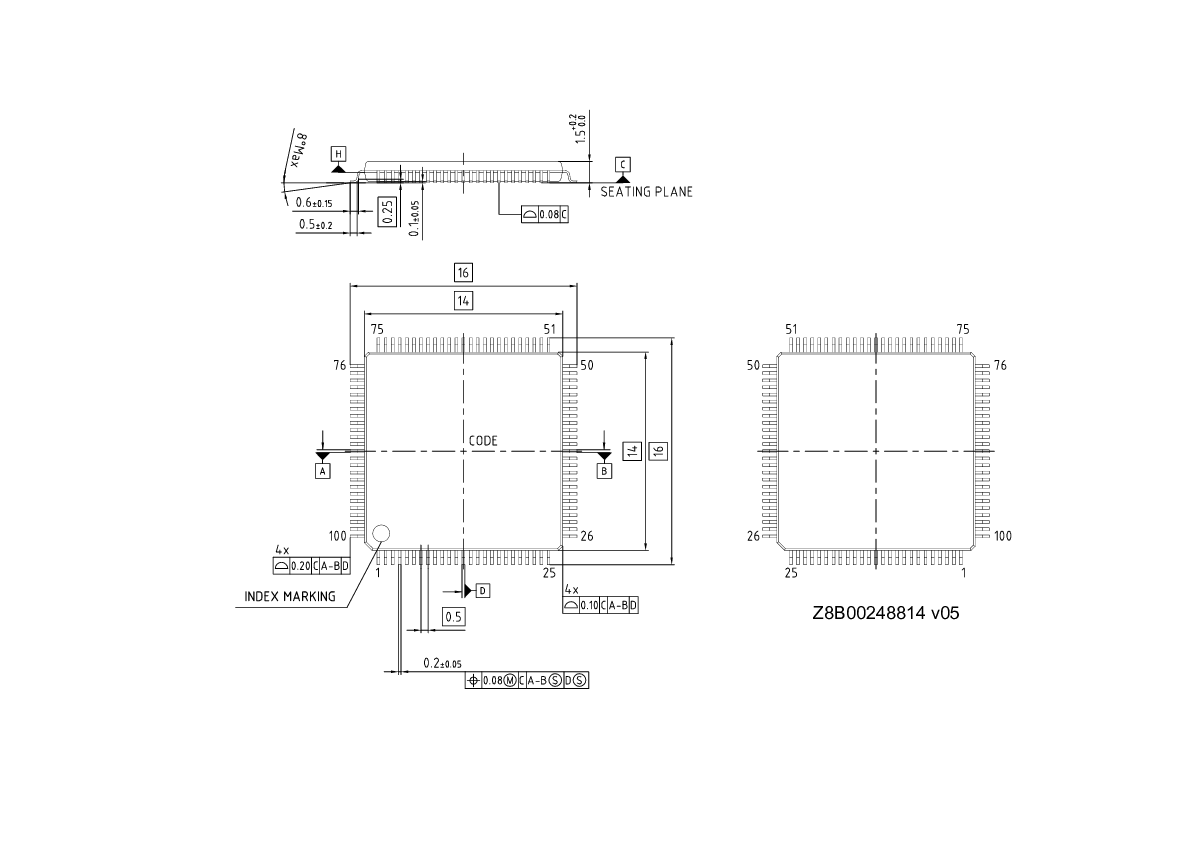
Figure 37.
80-LQFP package outline (PG-LQFP-80)
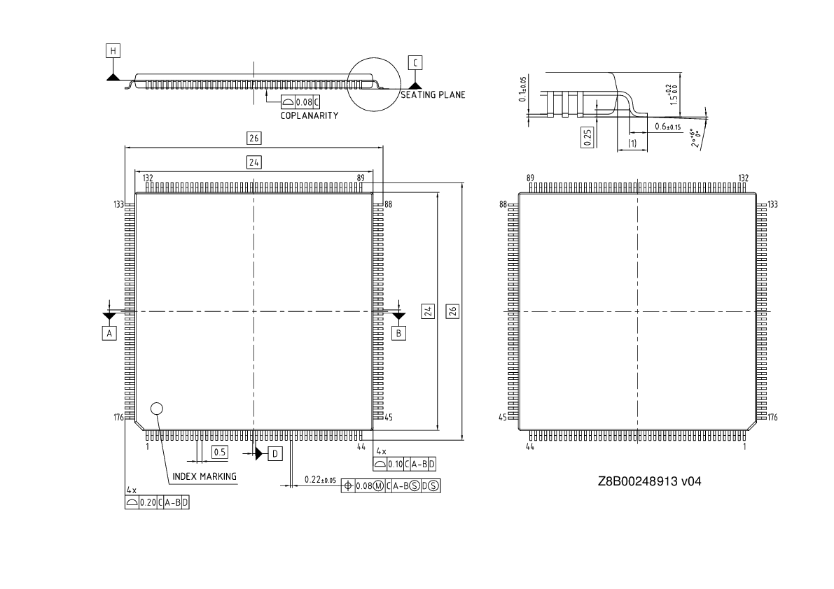
Figure 38.
64-LQFP package outline (PG-LQFP-64)
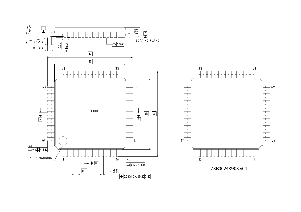
Appendix
Bootloading or end-of-line programming
Triggered at device startup, if a trigger condition is applied
Either CAN or LIN communication may be used
Bootloader polls for the communication on CAN or LIN at separate time frames, until the overall 300-second timeout is reached
If a bootloader command is received on either communication interface, the polling stops and bootloader starts using this interface
Figure 39.
Bootloading sequence
Sl. No. | CAN interface | Configuration |
|---|---|---|
1 | CAN Mode | Classic CAN |
2 | CAN Instance | CAN0, Channel#1 |
3 | CAN TX | P0.2/CAN0_1_TX |
4 | CAN RX | P0.3/CAN0_1_RX |
5 | CAN Transceiver NSTB/EN (Low) | P23.3 (optional) |
6 | CAN Transceiver EN/EN (High) | P2.1 (optional) |
7 | CAN RX Message ID | 0x1A1 |
8 | CAN TX Message ID | 0x1B1 |
9 | Baud | 100 or 500 kbps alternating |
Figure 40.
MCU to CAN transceiver connections
Sl. No. | LIN interface | Configuration |
|---|---|---|
1 | LIN Type | LIN0, Channel#1 |
2 | LIN Mode | Slave |
3 | LIN Checksum Type | Classic |
4 | LIN TX | P0.1/LIN1_TX |
5 | LIN RX | P0.0/LIN1_RX |
6 | LIN EN/EN (High) | P2.1 (optional) |
7 | LIN EN (Low) | P23.3 (optional) |
8 | LIN TX PID | 0x46 |
9 | LIN RX PID | 0x45 |
10 | Baud | 20 or 115.2 kbps |
11 | Break Field Length | 11 |
12 | Break Delimiter Length | 1 bit |
Figure 41.
MCU to LIN transceiver connections
External IP revisions
Module | IP | Revision | Vendor |
|---|---|---|---|
CANFD | mxttcanfd | M_TTCAN IP revision: Rev.3.2.3 | Bosch |
Arm® Cortex®-M0+ | armcm0p | Cortex®-M0+-r0p1 | Arm® |
Arm® Cortex®-M4F | armcm4 | Cortex®-M4-r0p1 | Arm® |
Arm® Coresight | armcoresighttk | CoreSight-SoC-TM100-r3p2 | Arm® |
Acronyms
Acronym | Description |
|---|---|
A/D | Analog-to-Digital |
ABS | Absolute |
ADC | Analog-to-Digital converter |
AES | Advanced encryption standard |
AHB | AMBA (advanced microcontroller bus architecture) high-performance bus, Arm® data transfer bus |
Arm® | Advanced RISC machine, a CPU architecture |
ASIL | Automotive safety integrity level |
BOD | Brown-out detection |
CAN FD | Controller Area Network with Flexible Data rate |
CMOS | Complementary metal-oxide-semiconductor |
CPU | Central Processing Unit |
CRC | Cyclic redundancy check, an error-checking protocol |
CSV | Clock supervisor |
CTI | Cross trigger interface |
DES | Data encryption standard |
DFT | Design-For-Test |
DW | Datawire same as P-DMA |
ECC | Error correcting code/Elliptical curve cryptography |
ECO | External crystal oscillator |
ETM | Embedded Trace Macrocell |
EVTGEN | Event Generator |
FLL | Frequency-locked loop |
FPU | Floating point unit |
GHS | Green Hills tool chain with Multi IDE |
GPIO | General purpose input/output |
HSM | Hardware security module |
I/O | Input/output |
I 2 C | Inter-Integrated Circuit, a communications protocol |
ILO | Internal low-speed oscillator |
IMO | Internal main oscillator |
IOSS | Input/output sub-system |
IPC | Inter-processor communication |
IrDA | Infrared interface |
IRQ | Interrupt request |
JTAG | Joint test action group |
LDO | Low drop out regulators |
LIN | Local Interconnect Network, a communications protocol |
LVD | Low voltage detection |
OTA | Over-the-air programming |
OTP | One-time programmable |
OVD | Over voltage detection |
P-DMA | Peripheral-Direct Memory Access same as DW |
PLL | Phase-locked loop |
POR | Power-on reset |
PPU | Peripheral protection unit |
PRNG | Pseudorandom number generator |
PWM | Pulse-width modulation |
MCU | Microcontroller Unit |
MCWDT | Multi-counter watchdog timer |
M-DMA | Memory-Direct Memory Access |
MISO | SPI Master-in slave-out |
MMIO | Memory mapped I/O |
MOSI | SPI Master-out slave-in |
MPU | Memory protection unit |
MTB | Micro trace buffer |
MUL | Multiplier |
MUX | Multiplexer |
NVIC | Nested vectored interrupt controller |
RAM | Random access memory |
RISC | Reduced-instruction-set computing |
ROM | Read only memory |
RSA | Rivest-Shamir-Adleman Public Key Encryption Algorithm |
RTC | Real-time clock |
SAR | Successive approximation register |
SCB | Serial communication block |
SCL | I 2 C serial clock |
SDA | I 2 C serial data |
SECDED | Single error correction, double error detection |
SHA | Secure hash algorithm |
SHE | Secure hardware extension |
SMPU | Shared memory protection unit |
SPI | Serial peripheral interface, a communications protocol |
SRAM | Static random access memory |
SWD | Serial wire debug |
SWJ | Serial wire JTAG |
TCPWM | Timer/Counter Pulse-width modulator |
TTL | Transistor-transistor logic |
TRNG | True random number generator |
UART | Universal Asynchronous Transmitter Receiver |
WCO | Watch crystal oscillator |
WDT | Watchdog timer reset |
Revision history
Document revision | Date | Description of changes |
|---|---|---|
** | 2020-02-07 | New datasheet |
*A | 2020-06-29 | Changed datasheet status to Preliminary. Updated Features list :
Updated ILO Clock Source description in Clock system . Updated the block of CLOCK_PATH3 in the CYT2B6 clock diagram . Updated VCCD in Power pin assignments . Removed associated footnotes in Table 16 . Added Table 16 . Updated MUX Group 10 in Table 20 . Updated Table 23 . Updated Table 24 . Updated Table 27 . Updated Figure 12 Updated Ordering information . Updated Table 58 and Table 59 . Added note in Table 61 . Added External IP revisions . |
*B | 2021-07-08 | Updated Features . Updated Features list . Updated Communication peripheral instance list . Updated System resources . Updated I/Os . Updated High-speed I/O matrix connections Updated Alternate function pin assignments Updated Triggers one-to-one Updated Faults Updated Miscellaneous configuration . Updated Electrical specifications . Updated Part number nomenclature . Updated Appendix . Updated Errata. |
*C | 2022-10-07 | Migrated to IFX template. Updated Clock system . Updated Pin assignment . Updated Alternate function pin assignments Updated Packaging . Updated Errata. |
*D | 2023-07-12 | Updated title to ‘Based on Arm® Cortex®-M4F single’. Updated Features list . Updated Blocks and functionality . Updated Peripheral I/O map . Updated Package pin list and alternate functions . Updated Power pin assignments Updated Alternate function pin assignments . Updated Trigger multiplexer . Updated Triggers one-to-one Updated Packaging . Updated Errata. |
*E | 2024-03-04 | Updated Triggers one-to-one Updated Errata. |
*F | 2025-06-10 | Updated PLL and FLL Updated Table 38 Removed Errata. |
*G | 2026-03-10 | Updated General description . Updated Features . Updated Features list . Updated Clock specifications . Updated template. Updated footnote numbers. |
Revision history change log
Section | Change description | Current spec | New spec | Reason for change |
|---|---|---|---|---|
General description | Added description | None | Infineon's TRAVEO™ T2G 32-bit Automotive MCU is a high-performance, low-power controller designed for automotive applications, compliant to ISO 26262 for functional safety and ISO 21434 for cybersecurity. | Addition |
Features | Updated description | Crypto engine | ISO 21434 compliant / EVITA Full | Updated |
Features | Updated description | Functional safety for ASIL-B | ISO 26262 functional safety compliant for ASIL-B | Updated |
Features list | Updated description | Functional safety | ASIL-B | Functional safety | ISO 26262 ASIL-B compliant | Updated |
Features list | Updated description | Security | Security - ISO 21434 compliant | Updated |
Features list | Added Note | Analog 3 Units (SAR0/11, SAR1/13, SAR2/8 logical channels | Analog 3 Units (SAR0/11, SAR1/13, SAR2/8 logical channels 1)
| Addition |
27.12 Clock specifications | Updated description for Note for ECO connection scheme | 17: Refer to the family-specific Architecture TRM for more information on crystal requirements (002-19314,TRAVEO™ T2G Automotive MCU body controller entry architecture technical reference manual). | 17: Refer to the family-specific Architecture TRM for more information on crystal requirements (002-19314,TRAVEO™ T2G Automotive MCU body controller entry architecture technical reference manual). Before enabling ECO, the TRIM registers (ATRIM, WDTRIM, FTRIM, GTRIM and RTRIM) shall be configured with correct settings based on and User Guide "Setting ECO parameters, TRAVEO™ T2G family" (Doc No. 002-30194) and the crystal matching test from the crystal vendor. | Updated |
1 The Crypto engine features are available on select MPNs.
2 This feature is not available in “eSHE only” parts; for more information, refer to Ordering information .
4 Enhanced Secure Hardware Extension (eSHE) is enabled by third-party firmware.
5 GPIO_STD supporting 2.7 V to 5.5 V V DDIO range.
6 GPIO_ENH supporting 2.7 V to 5.5 V V DDIO range with higher currents at lower voltages.
7 Operation of reference-timed peripherals (like a UART) with an FLL-based reference is not recommended due the allowed frequency error.
8 VREF_L prevents IR drops in the VSSIO and VSSA paths from impacting the measurements. VREF_L, when properly connected, reduces or removes the impact of IR drops in the VSSIO and VSSA paths from measurements.
9 I/Os drive level does not support the full bus capacitance in Fast-mode Plus speeds.
10 This is not 100% compliant with the I 2 C-bus specification; I/Os are not over-voltage tolerant, do not support the 20-mA sink requirement of Fast-mode Plus, and violate the leakage specification when no power is applied.
11 Only Port 0 with the slew rate control enabled meets the minimum fall time requirement.
12 The Easy SPI (EZSPI) protocol is based on the Motorola SPI operating in any mode (0, 1, 2, or 3). It allows communication between master and slave reduces the need for CPU intervention.
13 The Easy I 2 C (EZI2C) protocol is a unique communication scheme built on top of the I 2 C protocol by Infineon. It uses a meta protocol around the standard I 2 C protocol to communicate to an I 2 C slave using indexed memory transfers. This reduces the need for CPU intervention.
14 The I/Os in VDDIO_1 domain are referred to the VDDD domain in 64-LQFP package.
15 The size representation is not up to scale.
16 First 2 KB of SRAM is reserved, not available for users. User must keep the power of first 32KB block of SRAM0 in enabled or retained in all Active, LP Active, Sleep, LP Sleep, DeepSleep modes.
17 These six Programmable PPUs are configured by the Boot ROM and are available for the user based on the access rights. Refer to the device specific TRM to know more about the configuration of these programmable PPUs.
18 Port configuration of SWD/JTAG pins will be changed from the default GPIO mode to support debugging after the boot process, refer to Table 14 for pin assignments.
20 All port pin functions available in DeepSleep mode are also available in Active mode.
22 DeepSleep ordering (DS #0, DS #1, DS #2) does not have any impact on choosing any alternate functions; the HSIOM module handles the individual alternate function assignment.
23 I/O pins that support an oscillator function (WCO or ECO) must be configured for high-impedance if the oscillator is enabled.
The V CCD pins must be connected together to ensure a low-impedance connection. (see the requirement in Figure 12 ).
26 For any function marked with an identifier (n), the AC timing is only guaranteed within the respective group "n".
28 Active Mode ordering (ACT#0, ACT#1, and so on) does not have any impact on configuring alternate functions; the HSIOM module handles the alternate function assignments.
29 User interrupt cannot be used for CM0+ application, as it is used internally by system calls. Note, this does not impact CM4 application
30 The diagram shows only the TRIG_LABEL, final trigger formation is based on the formula TRIG_(PREFIX(IN/OUT))(MUX_x)(TRIG_LABEL) / TRIG_(PREFIX(IN_1TO1/OUT_1TO1))(x)(TRIG_LABEL) and the below mentioned tables Table 20 , Table 21 , and Table 22 .
31 “a:b” depicts a range starting from ‘a’ through ‘b’.
32 Each logical channel of SAR ADC[x] can be connected to any of the SAR ADC[x]_y external pin. (x = 0, or 1, or, 2 and y=0 to max 31)
33 Fixed PPU is configured inside the Boot and user is not allowed to change the attributes of this PPU.
34 These parameters are based on the condition that V SSD = V SSA = 0.0 V.
35 The I/Os in V DDIO_1 domain are referred to the V DDD domain in 64-LQFP package.
36 A current-limiting resistor must be provided such that the current at the I/O pin does not exceed rated values at any time, including during power transients. Refer to Figure 11 for more information on the recommended circuit.
37 V DDIO and V DDD must be sufficiently loaded or protected to prevent them from being pulled out of the recommended operating range by the clamp current.
38 When the conditions of 36 , 37 , and SID18A/B/C/D are met, |I CLAMP_ABS | supersedes V IA_ABS and V I_ABS
39 The definition of “closer” depends on the package. In LQFP packaging, “closest” is determined by counting pins. For example, in a 176-LQFP package, P17.4 (pin 120) is closer to the V DDD on pin 110 than on pin 132. Ports 11 and 21 should not be used for injection currents. The impact of injection currents is only defined for GPIO_STD/GPIO_ENH type I/Os.
40 The maximum output current is the peak current flowing through any one I/O.
41 The total output current is the maximum current flowing through all I/Os (GPIO_STD, and GPIO_ENH).
42 +B is the positive battery voltage around 45 V.
43 V DDD , V DDIO_1 , VDDIO_2 , and V DDA do not have any sequencing limitation and can establish in any order. These supplies (except for V DDA and V DDIO_2 ) are independent in voltage level. See 12-Bit SAR ADC DC Specifications when using ADC units.
44 3.0 V ±10% is supported with a lower BOD setting option for V DDD and V DDA . This setting provides robust protection for internal timing but BOD reset occurs at a voltage below the specified operating conditions. A higher BOD setting option is available (consistent with down to 3.0 V) and guarantees that all operating conditions are met.
45 5.0 V ±10% is supported with a higher OVD setting option for V DDD and V DDA . This setting provides robust protection for internal and interface timing, but OVD reset occurs at a voltage above the specified operating conditions. A lower OVD setting option is available (consistent with up to 5.0 V) and guarantees that all operating conditions are met. Voltage overshoot to a higher OVD setting range for V DDD and V DDA is permissible, provided the duration is less than 2 hours cumulated. Note that during overshoot voltage condition electrical parameters are not guaranteed.
46 eFuse programming must be executed with the part in a “quiet” state, with minimal activity (preferably only JTAG or a single LIN/CAN channel on V DDD domain, no activity on V DDIO_1 ).
47 Smoothing capacitor, C S1 is required per chip (not per V CCD pin). The V CCD pins must be connected together to ensure a low-impedance connection (see the requirement in Figure 12 ).
48 Capacitors used for power supply decoupling or filtering are operated under a continuous DC-bias. Many capacitors used with DC power across them provide less than their target capacitance, and their capacitance is not constant across their working voltage range. When selecting capacitors for use with this device, ensure that the selected components provide the required capacitance under the specific operating conditions of temperature and voltage used in your design. While the temperature coefficient is normally found within a parts catalog (such as, X7R, C0G, Y5V), the matching voltage coefficient may only be available on the component datasheet or direct from the manufacturer. Use of components that do not provide the required capacitance under the actual operating conditions may cause the device to operate to less than datasheet specifications
49 At cold temperature –5°C to –40°C, the DeepSleep to Active transition time can be higher than the max time indicated by as much as 20 μs.
50 If longer pulse suppression width is required, use Smart I/O.
51 V DDD must be greater than 0.8 × V DDA when ADC[2] is enabled. V DDIO_1 must be greater than 0.8 × VDDA when ADC[0] is enabled.
52 In order to drive full bus load at 400 kHz, 6 mA I OL is required at 0.6 V V OL .
53 In order to drive full bus load at 1 MHz, 20 mA I OL is required at 0.4 V V OL . However, this device does not support
54 The code-flash includes a 'Write Buffer' of 4096-bit. If the application software writes this buffer multiple times, to get the overall write time multiply one sector write time with the corresponding factor (say for factor 64, example, 64 x 512 B = 32 KB [one sector]).
55 Intermediate clocks that are not listed have the same limitations as that of their parent clock.
56 Mainly depends on the external crystal.
57 Refer to the family-specific Architecture TRM for more information on crystal requirements (002-19314,TRAVEO™ T2G Automotive MCU body controller entry architecture technical reference manual). Before enabling ECO, the TRIM registers (ATRIM, WDTRIM, FTRIM, GTRIM and RTRIM) shall be configured with correct settings based on and User Guide "Setting ECO parameters, TRAVEO™ T2G family" (Doc No. 002-30194) and the crystal matching test from the crystal vendor.
58 Please refer to family-specific Architecture reference manual for more information on crystal requirements (002-19314, TRAVEO™ T2G Automotive MCU body controller entry architecture technical reference manual).
59 Mainly depends on the external crystal.
60 Supported shipment types are “Tray” (default) and “Tape and Reel”. Add the character ‘T’ at the end to get the ordering code for “Tape and Reel” shipment type.
61 3DES/SHA-1/SHA-2/SHA-3/CRC/Vector unit for asymmetric cryptography features are not supported.
62 Code-flash size 576 KB = 14 KB × 30 (Large Sectors) + 8 KB × 16 (Small Sectors)
63 Work-flash size 64 KB = 2 KB × 24 (Large Sectors) + 128 B × 128 (Small Sectors)
64 S-grade Temperature (–40°C to 105°C).
65 JTAG ID CODE bits 12 through 27, represents the Silicon ID of the device.
66 E-grade Temperature (–40°C to 125°C).
67 The numbers are estimated values based simulation only and are based on a single bill of material combination per package type.
68 a1 = CTE (Coefficient of Thermal Expansion) value below T g (ppm/°C) (T g is glass transition temperature which is 131°C).
69 a2 = CTE value above T g (ppm/°C).
70 Board condition complies to JESD51-7(4 Layers)
71 Maximum value °C/Watt shown is for T A = 125°C.