AN2009-01 Assembly Instructions for the Easy-PressFIT modules
About this document
Scope and purpose
This application note provides a guideline on how to use and implement Easy modules using PressFIT connectors. The values and recommendations provided in this document should not be considered as datasheet values.
Intended audience
This document is intended for all experts using Infineon Easy modules.
General information
PressFIT is an alternative method for connecting control and load current contacts on IGBT modules to a PCB (printed circuit board) that complies with the requirements for greater durability, the trend towards higher temperatures, RoHS and, of course, very simple handling.
This contact technology has already been employed for years in the automotive sector under the most difficult of conditions, and with medium-sized currents. The contacts have also been used in the telecommunications sector for some time now for signal transmissions. This type of contact is therefore ideal for use in IGBT modules for which the contacts have to meet the requirements for load, control and sense connections.
The PressFIT contact technology for power modules was initially developed in the EconoPIM™ and EconoPACK™ series.
The Easy PressFIT pin provides a solution for modules without a baseplate. It should be noted in the case of the Easy PressFIT geometry that it has been used for decades in a wide variety of applications, and has been adapted for use in the various modules.
The Easy PressFIT contact allows solderfree assembly of the EasyPIM™, EasyPACK and Easy Automotive modules in the EasyB series. In this assembly technology, the module can be mounted on either side of the circuit board.
The electrical and thermal contacts with the circuit board are implemented by means of cold welding. The contacts can be used in standard FR4 PCB with the typical tolerances of manufacturers.
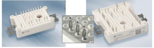
Figure 1. Modules in the EasyB series featuring PressFIT contacts
Easy PressFIT contacts have an area of approximately 1.7 mm that adapts itself to the hole in the PCB during the press-in process. The plastic is deformed as a result. This deformation is intended to accommodate the tolerance, and provides the basis for the cold welding.
The forces resulting during the PressFIT process ensure that the welded materials on the PCB and pin exhibit a continuously consistent – and, unlike other contact technologies – very small electrical contact resistance (approximately 0.05 mΩ).
Figure 2
shows various sections and REM images that provide a view of the gas-tight bonded materials resulting from the press-in force.
Figure 2. Easy PressFIT contact sections
General information on power module handling
This section describes forces on module housing – DCB push-out
The power module is not designed to withstand forces on the module housing as shown in the example of Figure 3. The module pins are located here on a flat table. Forces on the module housing (Fp) are pushing the DCB out of the housing. Therefore, forces (Fp) on the module housing have to be avoided during handling. Please note that this is a different case compared to the normal press-in process, where the DCB is fully supported in the press-tool, and the press-in forces affect the DCB, and not the housing.
Figure 3. Forces on the housing during module handling should be avoided to prevent a push-out of the DCB
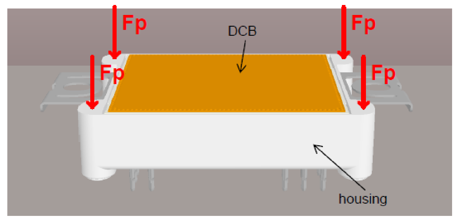
Some modules will have quite low DCB push-out forces (Fp), the minimum value of which is not a confirmed property of the power module. This is not critical for real applications, because the housing is fixed later on the cooling system by the integrated clamps. So, the housing cannot move in a critical way. Furthermore, the “sealing rope” between the module frame and the DCB only serves to seal the module when the isolating gel is filled during our production process. After the filling process, the liquid gel is heated and becomes soft but solid. The sealing has no gluing function in the final product.
Requirements for printed circuit boards
The PressFIT technology used in the Easy modules has been inspected and qualified by Infineon Technologies AG for standard FR4 PCBs with tin applied chemically (IEC 60352-5+ IEC60747-15). If other handling technologies are to be used in the production of PCBs, they have to be tested, inspected and qualified.
Requirements for the PCB material:
Double-sided PCB according to IEC 60249-2-4 or IEC 60249-2-5.
Multilayer PCB according to IEC 60249-2-11 or IEC 60249-2-12.
Minimum | Typical | Maximum | |
|---|---|---|---|
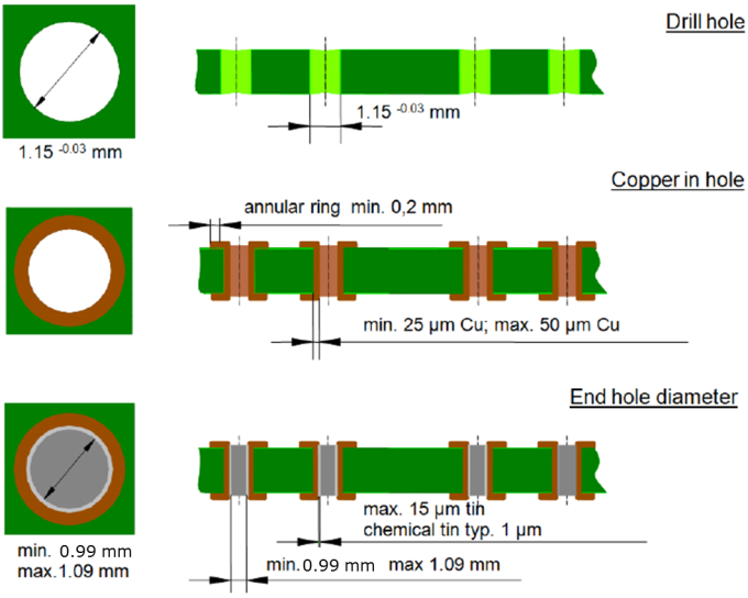
Hole drill diameter | 1.12 mm | 1.15 mm | |
Copper thickness in hole | > 25 µm | < 50 µm | |
Metallization in hole | < 15 µm | ||
End hole diameter | 0.99 mm | 1.09 mm | |
Copper thickness of conductors | 35 µm | 70 µm 105 µm | 400 µm |
Metallization of circuit board | Tin (chemical) recommended | ||
Metallization of pin | Tin (galvanic) | ||
In order to ensure that the PressFIT contact sits securely in the PCB, the specification of the hole given in Table 1 must be adhered to.
If the specification of PressFIT holes is limited to only the finished dimension (that is, the metallized hole), different drill sizes could be used depending on the PCB manufacturer and production philosophy, and also different metallization thicknesses could be provided. This would lead to results that would have to be rejected for quality assurance reasons.
The end hole diameter is a function of the drill hole, the copper thickness and the metallization in the hole.
The recommendation still applies that the hole in the PCB is to be drilled during manufacture with a drill size of 1.15 mm, and should not be milled. Experience has shown that a final hole diameter between 1.12 mm and 1.15 mm is obtained under consideration of the runout tolerances of the spindles after drilling due to shrinking of the FR4 material.
With a copper thickness of 30 µm to 50 µm in the hole and a tin layer of about 1 µm for tin applied chemically, an end hole diameter is obtained as the test dimension. Due to the thinner tin layer thickness, this diameter is always higher than the value of 1 mm stated in the standard (IEC 60352-5). The final hole diameter, considering the drilling diameter, copper thickness and a chemical tin layer, is typically between 1.02 mm and 1.09 mm.
Figure 4. Structure of a PCB
The PressFIT technology is qualified for FR4 PCB material.
After a reflow soldering process is carried out on a PCB, the module can be pressed into the board without difficulty. The retention forces of the press-fitted pins are not diminished.
Depending on the applied press tools, a certain distance from the middle of the pins to other components must be observed.
A distance of 5 mm is recommended, similar to Infineon’s Econo PressFIT power modules.
A PressFIT module can be replaced up to two times. This means that a PCB can be used in total three times.
Correct handling of the components is essential.
A module that has been pressed in, and the contact pressed out again, can no longer be pressed back in again. Instead, the module can only be attached to a new PCB via soldering. The plastic deformation of the PressFIT area does not permit a further PressFIT process.
Tolerance of PCB hole pattern is suggested to be kept within:

The press-in process
This section deals with the necessary press-in forces and tools for the modules.
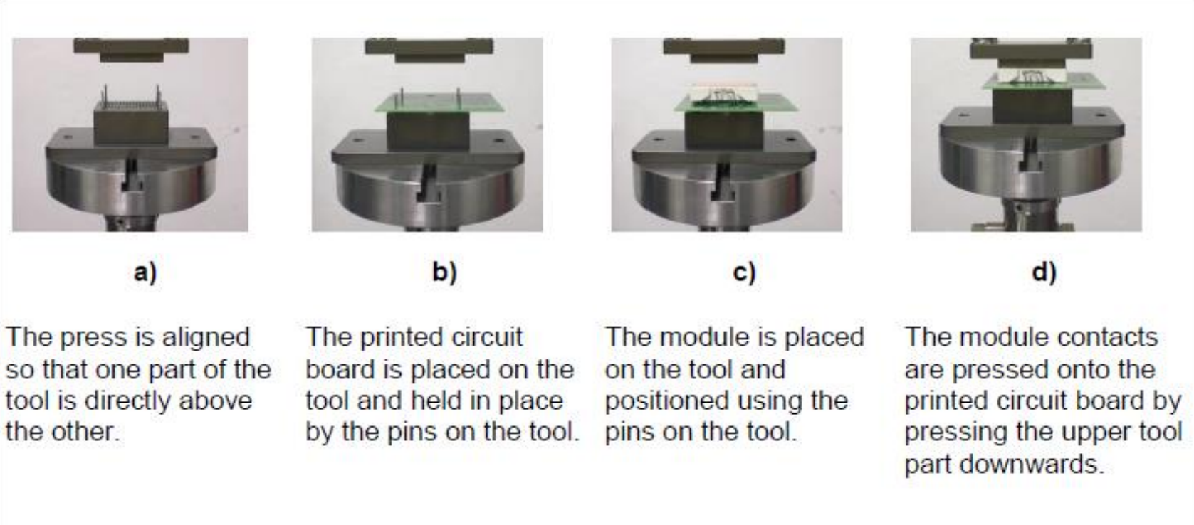
The PressFIT module is inserted in a PCB by pressing it in. PressFIT can be performed using a toggle lever press or a machine. A press-in tool that records the necessary force and the travel distance is recommended. Consistent quality and reproducability is assured in this way. The PressFIT speed should not be lower than 25 mm/min according to IEC 60352-5. A lower PressFIT speed can lead to increased press-in forces and to deformation of the pins, or a non gas-tight connection.
Note that during the press-in process, the placement area of the PCB and the pressing area of the pressure plate must be parallel to each other. The pressure plate should be mechanically fixed in position without any tolerance. The module is then pressed into the PCB in a regular motion.
The module pins should penetrate the PCB during press-in until the four stand-offs on the module, or optional distance keepers as described in
Multi-module and automotive application
, make contact with the board.
By adhering to the principles stated above, a smooth insertion process for the two components can be achieved.
The following illustrations show the press-in process as it is implemented in the laboratory.
Figure 5. Press-in process of an Easy module
Attention: It is recommended to protect the underside of the IGBT module against damage during the press-fitting process.
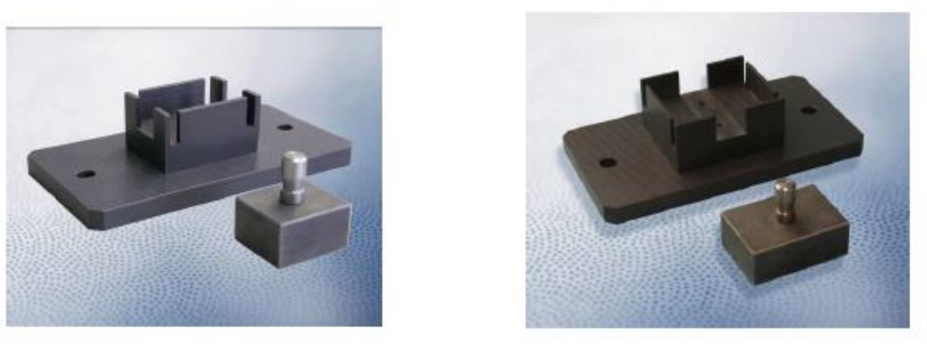
Press-in tools
The following tools that help pressing the modules in and out are recommended for the three Easy B Series modules.
Figure 6
shows these pressing tools for the two housing types, Easy 1B and Easy 2B. The pressing tools for Easy 3B housing are shown in
Figure 7
.
Each of the tools has two parts. The first part presses against the underside of the module, and the second part holds the PCB in place to be pressed against.
No components can be placed in the mounting areas of this special type of press-fitting tool. This prevents damage during the press-fitting process.
When press-fitting multiple modules onto a PCB, arrange the press-in tool in such a way that the modules are on the same level after pressing. In this way, the modules can be mounted on the heat sink with a good thermal connection.
Figure 6. Press-fitting tools for Easy1B (shown left), Easy2B (shown right)
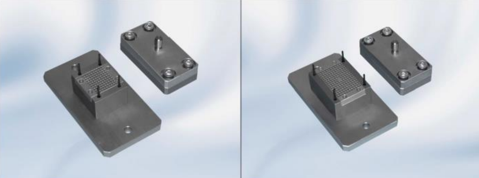
Figure 7. Press-fitting tools for Easy3B from HARTING Electronics GmbH
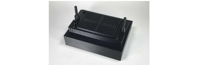
The drawing can be adjusted according to different requirements (e.g. module pinning and top side assembly of other parts) and the tools produced by a manufacturer of choice.
Press-in tools for Easy modules with thermal interface material
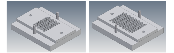
If modules with pre-applied thermal interface material (TIM) are used, the press-in stamp has to be designed with respect to the position of the TIM material on the module’s base plate.
Figure 8
shows the picture of an Easy2B module with TIM.
Figure 8. Easy2B with TIM

The structure of the presented TIM surface is only exemplary and not fixed for all products within the Easy family.
The stamp should not touch the TIM material during press-in. That is why the stamp only touches the substrate areas without TIM.
Figure 9
shows the geometries of the stamp for the press-in of Easy1B and Easy2B modules with TIM.
Figure 9. Press-in stamp of Easy1B (left) and Easy2B (right)
Press-in forces and speed
To press a module onto a PCB, a force of between approximately 60 N and 100 N must be applied for each pin in the module. The press-in forces vary according to the diameter of the hole and copper metallization in the PCB.
shows the PressFIT speed and the maximum PressFIT force per pin.
PressFIT speed | > 25·mm/min according to IEC 60352-5 qualification 100·mm/min recommended | |
PressFIT forces per pin | Typ. 85·N | <100·N maximum |
Attention: The maximum applied force per module for Easy1B and Easy2B during pressing should not exceed 4·kN. For Easy3B the maximum applied force should not exceed 8·kN.
The press-fitting speed should not be lower than 25 mm/min according to IEC 60352-5. Infineon recommends a press-in speed of about 100·mm/min. The typical press-in speed for automated assembly lines is up to 450·mm/min.
The press-out process
This section deals with the necessary press-out forces and tools for the modules.
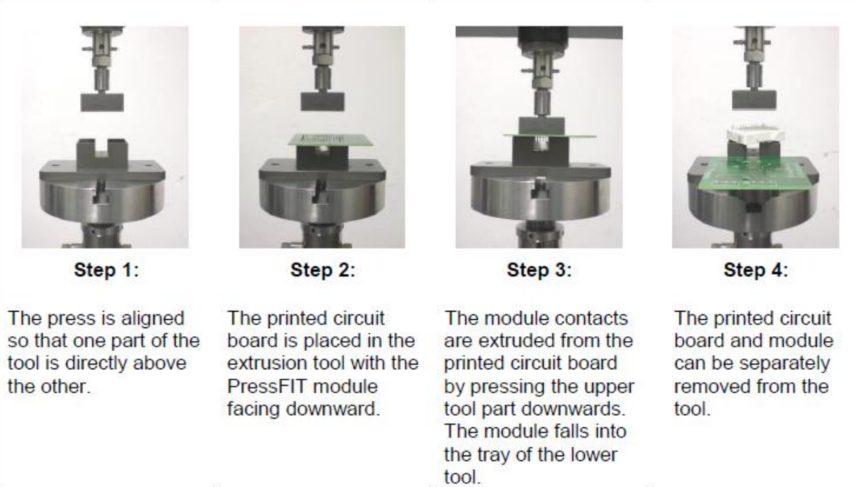
PressFIT modules are removed with the appropriate tools as shown in
Figure 10
and
Figure 11
. The PCB is placed with the PressFIT module on the device tray. Force is applied with the extrusion plate on the PressFIT pins that protrude from the PCB. The press-out tools must be aligned parallel to each other so that the individual components (such as the PCB and module) are not damaged. Once the PressFIT zone has been lifted from the PCB, the module falls onto the tray in the lower part of the tool, and is separated from the board.
Figure 10. Extrusion of an Easy module
Press-out tools
As already mentioned above, the press-out tools consist of two parts. The upper part of the tool presses directly downwards on the module pins. The lower part of the tool holds the module with the PCB, and serves as a base for the pressing operation.
The disassembly tools must be aligned parallel to each other in order to obtain an equally distributed extrusion process.
The dimensions of the press-out tool must be considered when designing the PCB so that the components positioned around the module will not be damaged.
Figure 11. Press-out tools for Easy1B (left) and Easy2B (right) modules
The drawing can be adjusted according to requirements and the tools produced by a manufacturer of choice.
Press-out forces
To press a module out of a PCB, a force of approximately > 40 N has to be applied for each pin in the module. The extruding forces depend mainly on the diameter of the hole in the PCB.
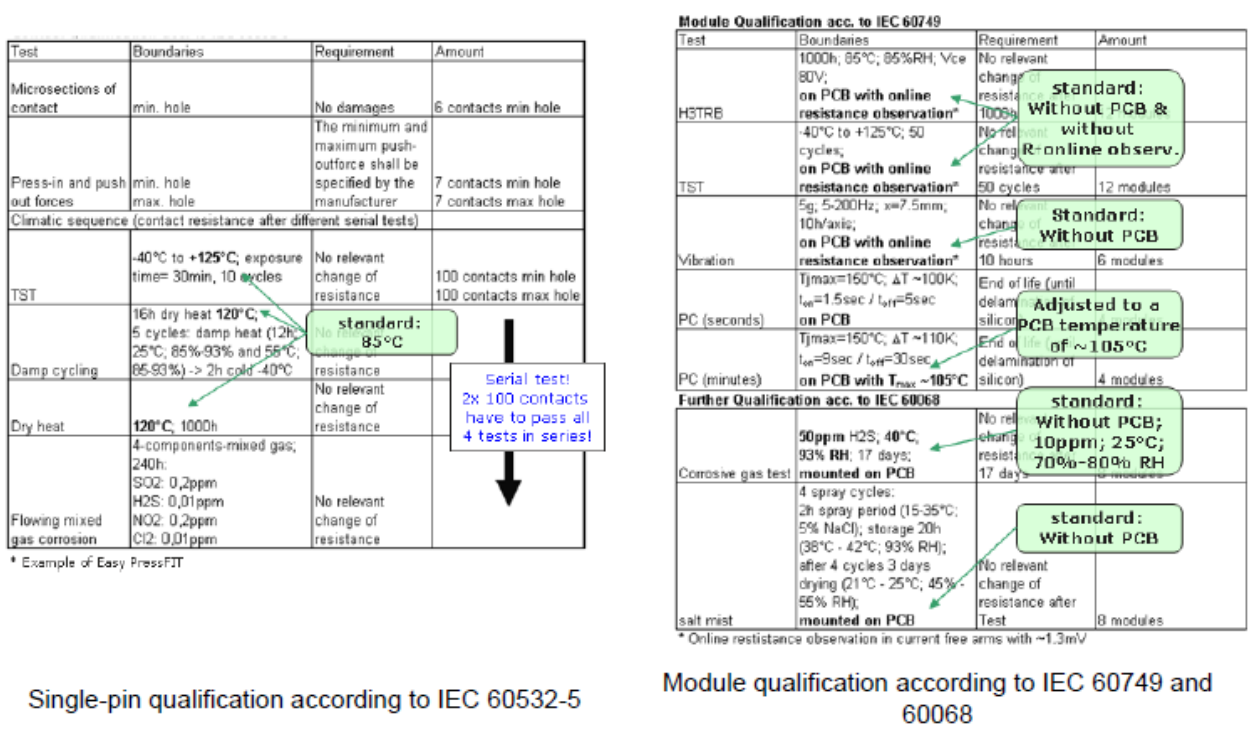
Quality of PressFIT contacts
PressFIT is an alternative solution for connecting control and load current contacts on IGBT modules with a PCB.
The requirements for greater durability, the trend towards higher temperatures and absence of lead, and, of course, very simple handling, are continuously growing.
As an advanced technology on the market, the PressFIT makes it possible to improve reliability up to a factor of 100 compared to manually soldered contacts and other contact types. The results of the reliability analyses in the Siemens norm SN 29500-5 demonstrate the factor.
The assembly process is simple, and consequently saves time and money. The process is reliable, and system reparability is ensured.
An extract from the Siemens norm SN 29500-5/Edition 2004-06 Part 5 shown in
Table 3
illustrates the failure rates of different contact technologies.
Process | Conductor diameter in mm 2 | Failure rate λref in FIT 1 | Notes: Standards/guidelines |
|---|---|---|---|
Solder manual Automatic | 0.5 0.03 | IPC 6102, class 2 | |
Wire bonding for hybrid circuits Al Automatic | 0.1 0.1 | 28 μm/wedge bond 25 μm/ball bond | |
Winding | 0.05 to 0.5 | 0.002 | DIN EN 60352 – 1/ IEC 60352 – 1 CORR1 |
Crimping manual Automatic | 0.05 to 300 | 0.25 | DIN EN 60352 – 2/ IEC 60352 – 2 A 1+2 |
Clips | 0.1 to 0.5 | 0.02 | DIN 41611 – 4 |
PressFIT | 0.3 to 2 | 0.005 | IEC 60352 – 5 |
Insulation piercing connectors | 0.05 to 1 | 0.25 | IEC 60352 – 3/IEC 60352 – 4 |
Screws | 0.5 to 16 | 0.5 | DIN EN 60999 – 1 |
Terminals (spring force) | 0.5 to 16 | 0.5 | DIN EN 60999 – 1 |
The PressFIT contact has been qualified in accordance with the usual standards for IGBT modules at Infineon.
shows a small extract of the various tests. The extract shows that the conditions in the individual tests are to be regarded as considerably stricter than stated in the standards. For example, in a corrosive gas test, the temperatures in scope of individual test is 15 K higher than the condition in the standard. And the H2S concentration is five times higher than the conditions according to the norm. The green fields show the test conditions according to the norm, which is less critical than in the individual tests.
Figure 12. Extract from qualification test
Further details on the individual tests can be found in various publications, such as "Reliability of PressFIT connections" at
.
Mounting a PCB to the module
For mounting a PCB onto the module, additional screws can be used if desired. These screws will be tightened into the stand-offs of the module.
An electronically controlled, or a slowly turning electric screwdriver, with n ≤ 300 rpm, is the preferred mounting tool.
Due to the lack of accuracy, we do not recommend the use of pneumatic screwdrivers or manual screwdrivers.
Figure 13. Detailed view of the assembly insert
The effective length of the thread in the stand-off should have a minimum of 4 mm and a maximum length of 8 mm.
The initial 1.5 mm of the mounting stand-off serves as guidance only and cannot take any force. The thread in the plastic will form during the screwing process.
For the choice of the screw length, the given PCB thickness has to be taken into account.
The following screws are tested to fix the PCB to the module:
Ejot PT WN 1451 K25*10 A2K M max= 0,45 Nm± 10%
Ejot DELTA PT WN 5451 K25*8 Mmax= 0,4 Nm± 10%
Metric screws: M2.5x – for example, M2.58 or M2.5*10 depending on the thickness of the PCB used
To avoid damage or splitting of the stand-off, straight insertion of the screw into the stand-off has to be observed during assembly.
Condition of the heat sink for module assembly
The power loss occurring in the module has to be dissipated via heat sink in order not to exceed the maximum permissible temperature T
vjop
specified in the datasheets during operation.
The condition of the heat sink surface in the area where the module is mounted is of great importance, as this interface between heat sink and module is of decisive influence on the heat transfer of the entire system.
The contact surfaces, the surface below the module and the surface of the heat sink have to be free of degradation and contamination to prevent excess mechanical stress to the module as well as an increase in thermal resistance.
Heat sink requirements:
Roughness: ≤ 10 µm
Flatness based on a length of 100 mm: ≤ 50 µm
Note: The flatness of the heat sink should not exceed the values listed above. This area includes the entire module mounting area as well as that of the clamps.
Note: If the layer of thermal grease applied is too thick, for example as a consequence of cavities, the thermal resistance Rth between module and heat sink will increase.
Applying the thermal grease
Due to the individual surface shape (e.g. roughness and flatness) of the heat sink and the module, the lower surface of the module and the surface of heat sink do not touch across the entire area. Therefore a certain localized separation between the two components cannot be avoided.
To dissipate the losses occurring in the module and to achieve a good flow of heat into the heat sink, all localized cavities have to be filled with a thermal compound. When using a heat conductive paste, a homogenous application needs to be assured.
A well-applied layer will fill all cavities, and at the same time will still allow the metallic contact between module base and heat sink surface. A compound should be selected which shows permanently elastic features in order to assure a continuously favorable heat transfer resistance.
Before the module is mounted onto the heat sink, an even layer of thermal grease, 80 µm thick for Easy1B/2B, and 60 µm thick for Easy3B, is recommended be applied to the module base or to the heat sink according to the module size and the thermal grease used. This grease can be applied using either a spatula, a roller, or by silk screen printing. The quantity of thermal grease is sufficient if a small amount of grease is visible around the module after assembly to the heat sink.
The recommendation is to apply the thermal grease by means of a screen print process. Apart from an optimized and module-specific distribution of the heat conductive paste, a homogenous and reproducible layer thickness can be achieved with this procedure. If a screen print process is used, the layer thickness could be reduced to values under the above-mentioned numbers. The size of the module and the viscosity of the thermal grease are important factors in this case.
Further notes regarding the application of screen print templates for the application of thermal grease can be found in the application note AN2006-02 Application of silk screen.
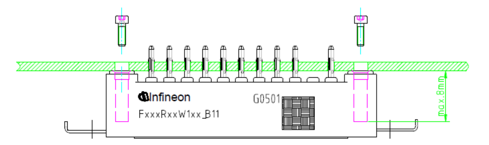
Assembling the module on heat sink
Assembling Easy1B/2B module on heat sink
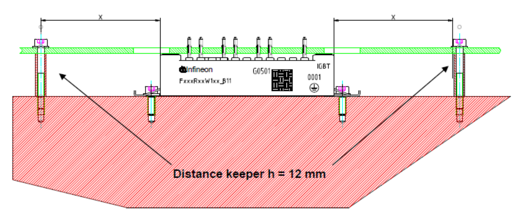
The module is mounted onto the heat sink using M4 screws. It is also possible to use an additional flat washer.
The heat sink has to be provided with threaded holes as shown in
Figure 14
.
Figure 14. Spacing of the threaded holes
Note: If the module is first pressed in to the PCB, or if a later disassembling of the module is desired, the PCB must contain suitable through-holes. The hole size depends on the screwdriver size or the screw’s head diameter or washer.
The module should be positioned onto the heat sink in such a way that the holes of the screw clamps are exactly above the threaded holes of the heatsink. The mounting surface must be clean and free of contamination.
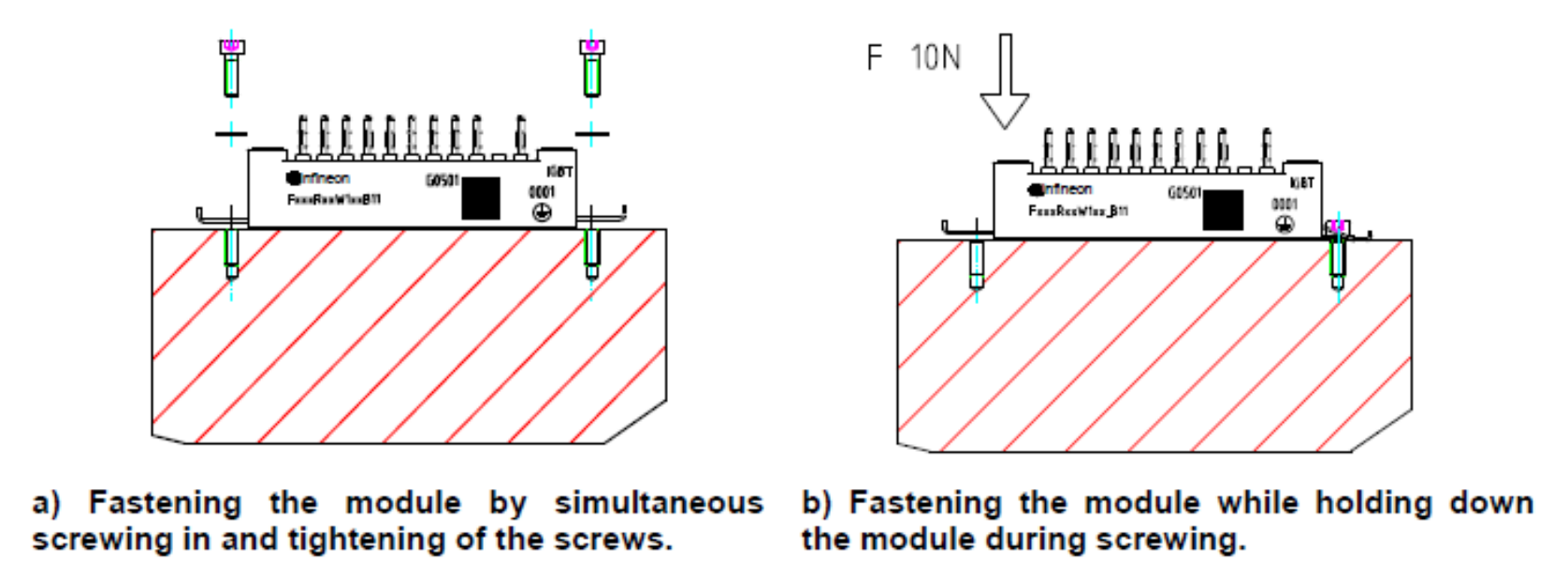
The module can be fastened by screwing in and tightening both screws at the same time (
Figure 15
a) or by holding down the module during the mounting process with a force of approximately 10 N so that the module cannot rise up (
Figure 15
b).
Figure 15. Module fastening options
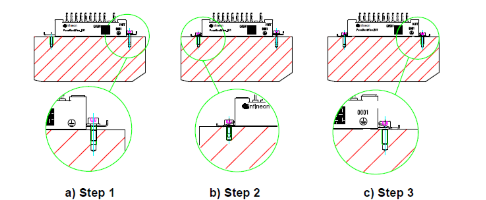
Alternatively, one screw can be applied initially. It is important that the module does not lift up. To prevent this, tighten the first screw loosely to avoid a press force to the clamp (
Figure 16
a). Then, tighten the second screw completely (
Figure 16
b). Finally, tighten the first screw completely (
Figure 16
c).
Figure 16. Fasten the module by tightening both screws at the same time
Description | Values |
|---|---|
Mounting screw | M4 |
Recommended mounting torque | Ma = 2.0 – 2.3 Nm |
Recommended thread engagement for screws with property class 4.8 to 6.8 for different materials | |
Aluminium cast alloy Aluminium alloy hardened Aluminium alloy not hardened | 2.2 x d = 8.8 mm 1.2 x d = 4.8 mm 3 1.6 x d = 6.4 mm 3 |
Washer acc. to DIN 125 | D = 9 mm |
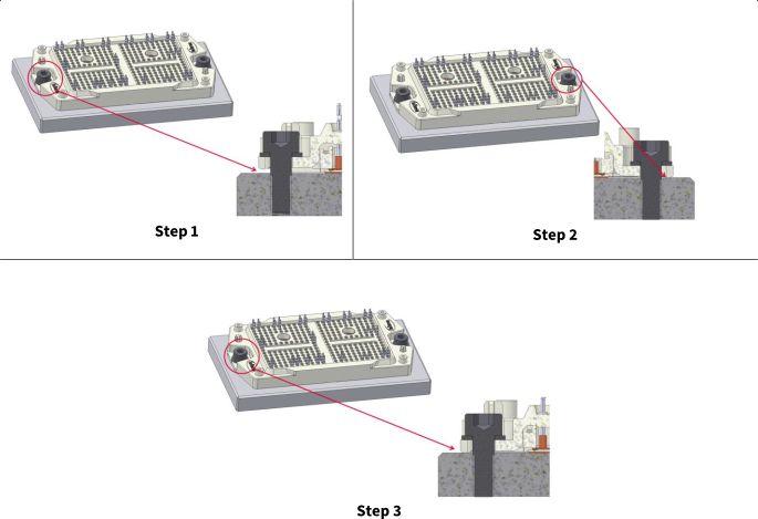
Assembling Easy3B module on heat sink
For the assembly of the Easy3B module to the heatsink, Infineon recommends the use of DIN M5 screws, in combination with a M5 washer.
Position the module correctly to the heat sink, so that the mounting area of the module is congruent with the threaded holes in the heat sink. Make sure that there are no foreign objects between the module and the heat sink.
The module can be fixed by screwing and tightening both screws at the same time (see
Figure 17
).
Figure 17. Steps for alternative fastening of the module

Alternatively, the module can be mounted to the heat sink in several steps (see
Figure 18
):
Step 1: The first screw can be screwed in slightly. Do not fully tighten it, so that no pressure is exerted
Step 2: The second screw needs to be firmly screwed to the heat sink
Step 3: Finally, the first (loose) screw needs to be screwed on firmly to the heat sink
Note: If the module is first pressed in to the PCB, or if a later disassembling of the module is desired, the PCB must contain suitable through-holes. The hole size depends on the screwdriver size or the screw’s head diameter or washer.
Figure 18. Module fastening steps
The following values are recommended for the mounting process:
Description | Values |
|---|---|
Mounting screw | M5 |
Recommended mounting torque | Mamax= 1.5 Nm |
Recommended property class of bolt | 4.6 – 5.6 |
Minimal thread length into the heatsink | 2 x d = 10 mm |
Pre-tightening torque | 0.3 – 0.5 Nm |
Tightening torque Ma | 1.3 – 1.5 Nm |
Screw velocity (pre-tightening) | U ≤ 250 U/min |
Screw velocity (tightening) | U ≤ 20 U/min |
Recommended washer | M5 |
System considerations
If the module is correctly mounted to the heat sink and to the PCB, the screw clamps will apply the necessary pressure. This pressure, together with the correct amount of thermal grease, will ensure a low thermal resistance and an optimal thermal flow between the module and the heat sink. Since the PCB is connected to the module by pressed-in pins only, suitable measures have to be taken to ensure that vibrations are kept at a minimum. Any possible movement between the terminals and the module case has to be avoided. Each single pin may only be subjected to a maximum press and pull force of 6 N vertical to the heat sink. The overall pulling force to the module of 20 N must not be exceeded. The compressive force could be 10 times higher than the possible pulling force. A low compressive load to the module is preferred. Therefore, the circuit board should additionally be fixed to the heat sink at a position close to the module. Two options are possible:
Figure 19. Fixing the PCB
Module is already pressed into the PCB before mounting
To minimize the forces that are applied to the pins of a module, it is recommended to keep a distance of at least x = 5 cm from the module’s outer edges (
Figure 19
).
Module is pressed into the PCB after mounting
In this case, no mechanical stress will occur. Therefore it is allowed to place the distance keeper as close as possible x ≤ 5 cm to the module.
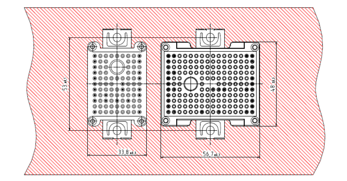
Clearance and creepage distances
When defining the layout of the PCB, application specific standards, mainly regarding clearance and creepage distances, have to be considered. This is particularly important for the area of the screw clamp, which is located under the PCB. In order to meet the respective requirements regarding clearance and creepage distances, current-carrying devices or through-holes in this area should be avoided, or additional isolation measures like lacquering must be taken.
Figure 20. Air path between clip and PCB for Easy1B and Easy2B packages
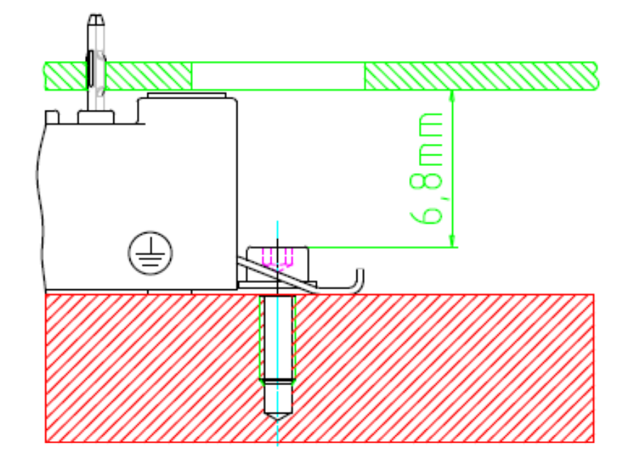
The minimum clearance distance between the screw and the PCB depends on the screw itself. For Easy1B and Easy2B packages, the distance will be 6.8 mm with a hexagon socket head M4 screw according to DIN 912, a washer according to DIN 125 and the clamp which can be seen in
Figure 20
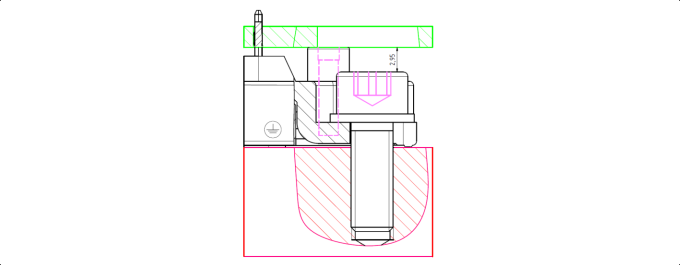
. For Easy3B packages, the distance will be 2.95 mm with a hexagon socket head M5 screw according to DIN 912, and an M5 washer according to DIN 125. A detailed drawing can be seen in
Figure 21
.
Figure 21. Air path between clip and PCB for Easy3B package
The clearance and creepage distances specified in the datasheet are minimum values irrespective of other devices that would be mounted close to the module.
In any case, the application-specific clearance and creepage distances have to be checked and compared to relevant standards and guaranteed by suitable constructive means, if required.
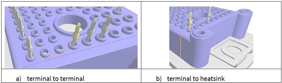
Creepage distance is defined as the shortest distance along the surface of a solid insulating material. For Easy modules, the outer and inner surfaces of the housing are considered. The terminal-to-terminal creepage distance refers to all relevant pins with different potentials, as shown in
Figure 22
.
Figure 22. Creepage distances for terminal to terminal and terminal to heatsink
Multi-module and automotive application
An increasing number of applications require the mounting of several power modules on the PCB. Furthermore, new power module applications, like automotive hybrid electrical vehicles and full electric vehicles (H)EV, have high requirements on vibration and mechanical shock robustness. In such applications the height tolerance of the modules has to be considered in the mounting concept in order to avoid a mechanical deformation of the PCB or unwanted forces on the modules and PressFIT pins.
Please note that the following instructions shall be regarded as additional information to the general mounting instructions. The chapter focuses on mounting concepts of the module, taking into account the height tolerance. General recommendations like PCB requirements, press speed, heat sink requirements, etc. are unaffected by the following instructions.
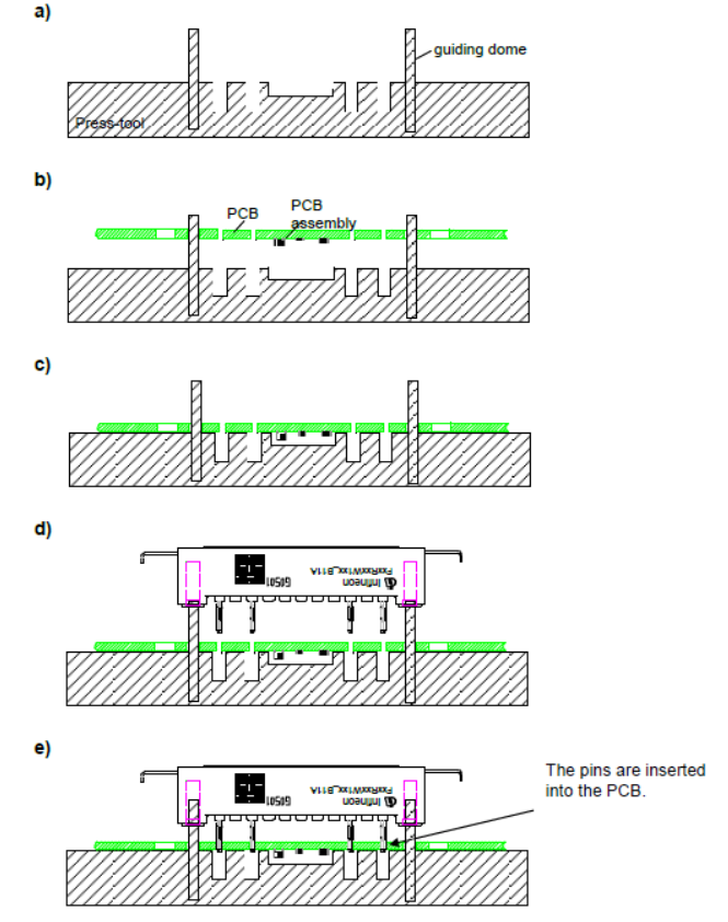
Modules’ press-in process on the PCB
shows the press-in process of the power modules on the PCB. This process is quite similar to that of Chapter 3.
a shows the bottom side of the press-tool with guiding domes, which are useful for pre-alignment. In
Figure 23
b, the PCB is placed into the press-tool, whereby the correct placement is obtained by the guiding domes of the press-tool.
c shows the press-tool with the PCB ready for module assembly.
In
Figure 23
d the module is placed on the guiding elements. The module is released and the module pins are inserted into the PCB.
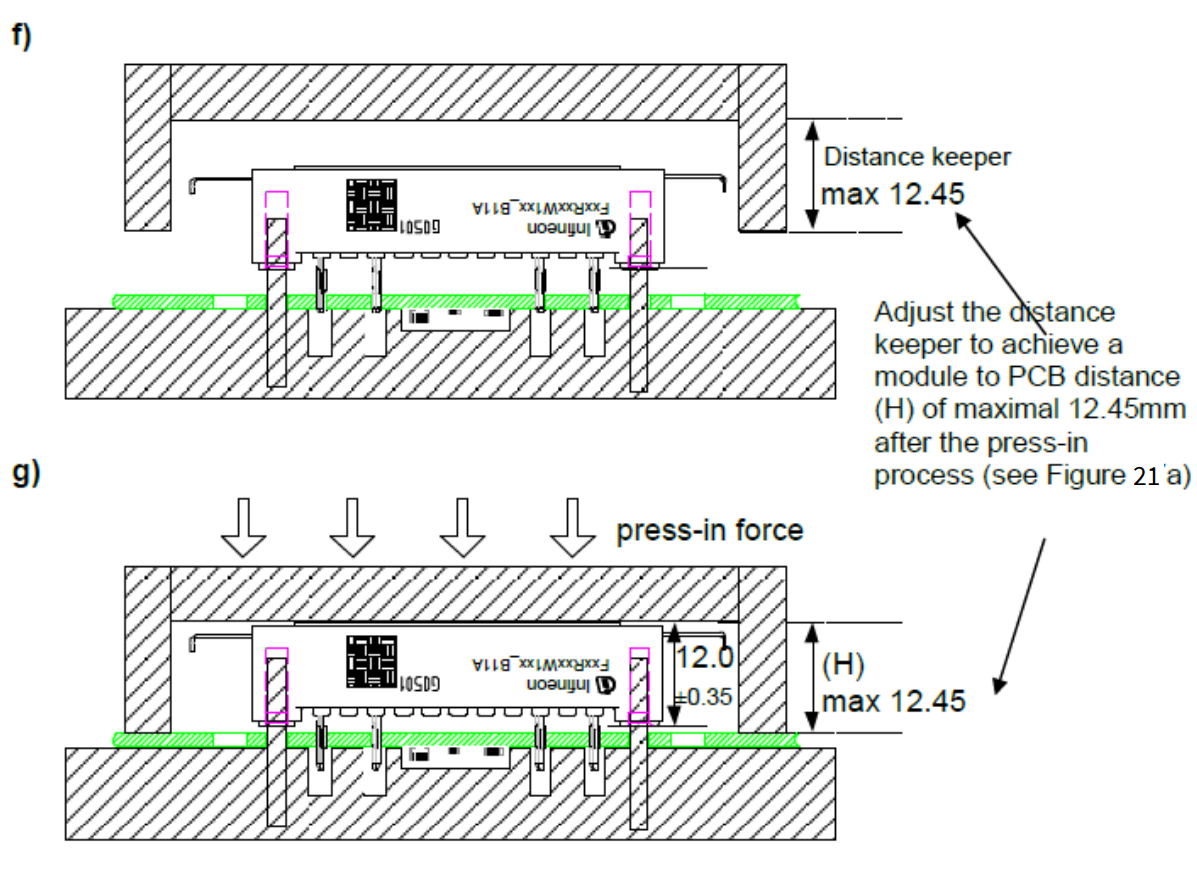
e shows the state where the module pins are inserted into the PCB. The module is now placed flush with the press-tool, and the pin touches the PCB at the beginning of the active press zone, which starts at about 2.5 mm from the pin top. If the module is not flush with the press-tool or pins are not inserted (module about 2.5 mm higher than the normal case shown here), then mounting should be corrected before the pins are damaged in the later press-in process.
In
Figure 23
f, the top press-tool with the distance keeper is shown.
g shows the controlled path-force press-in process. The press process stops by the increasing force between the PCB and this distance keeper. It is correct if the press-in process is stopped before the PCB is on the module housing. Thus, the distance of the module backside to the PCB is independent of the module height.
Note: It is possible to press the module tighter to the PCB than the maximum 12.45 mm. This will increase the overlapping zone in the active press zone (contact area: pin to PCB). Please do not forget to lower the fixing elements of the cooling system ( Figure 24 b) accordingly if the modules are pressed tighter to the PCB! The value (H) of Figure 24 b must not be higher than the module-to-PCB height of Figure 24 a! A force of the PCB on the module in the direction to the cooling system is uncritical and is desired, as it improves the thermal contact.
Figure 23. Press-in of the power modules (drawing not true to scale)
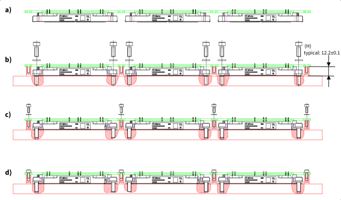
Modules and PCB mounting on the heat sink
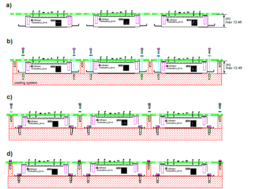
After the power module is pressed into the PCB (see
Figure 24
a), the PCB with the module has to be mounted to the cooling system. Please see
Chapter 7
and
Chapter 8
for more information on heat sink and thermal grease requirements, and how the grease should be applied to the system.
Figure 24
b-d show the mounting process with an example of three power modules pressed into the PCB. However, the illustrated concept can also be applied with a different number of modules or a single-module application.
Figure 24
b shows the process where the PCB with the pre-assembled modules is placed on the cooling system and the modules are fixed with screws via the spring clamp of the Easy module. Please refer to
Chapter 9
for detailed information on assembly of the modules on the heat sink. It is important to mount the modules before the PCB is fixed to the cooler!
c shows fixing of the PCB to the heatsink. As the height tolerance of the module is quasi compensated in the press process, the fixing points for the PCB can be close to the power modules. This is an advantage compared to the concept in section 10.1 where >= 5 cm distances have to be maintained between module and distance keepers.
The position of the distance keepers should be designed symmetrically around the power module(s).
d shows the final system assembly.
Figure 24. Mounting example of the PCB and module to the cooling system (drawing not true to scale)
The
Figure 25
shows a zoom of the final system assembly. Depending on the height of the module, a small air gap remains between module and PCB.
As the value (H) of
Figure 24
b must not be higher than the module-to-PCB height of
Figure 24
a, it is ensured that no pull forces are applied to the power modules, which would be critical in consideration of the thermal contact between module and heat sink.
Figure 25. Zoom illustration of final system assembly (drawing not true to scale)
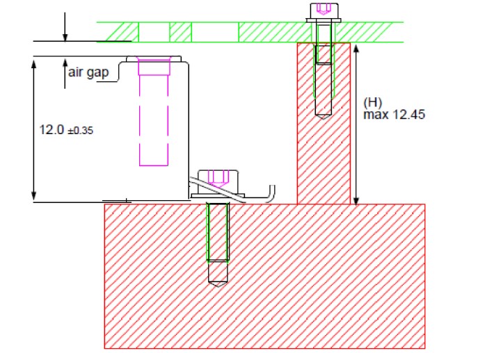
Please note that using this press concept with a remaining air gap does not allow the PCB to be screwed down to the stand-offs (guiding holes) as shown in
Chapter 6
.
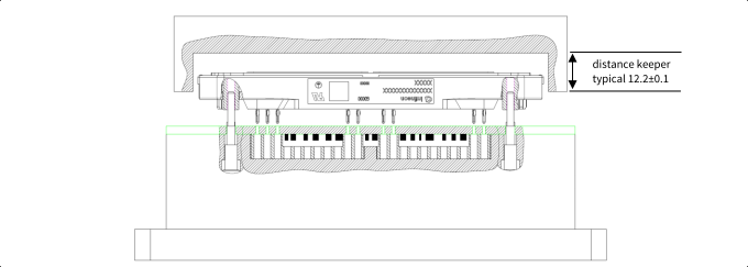
Press-in and mouting only Easy3B modules with PCB and heat sink
If only Easy3B modules are used in the system, in principle a shorter distance keeper can be applied. The general principle should be kept as descriped in
Chapters 12.1
and
Chapter 12.2
.
Figure 26. Typical distance keeper for Easy3B modules
In
Figure 27
a, the Easy3B module(s) is pressed into the PCB.
b shows the process where the PCB with the pre-assembled modules is placed on the cooling system, and the modules are fixed with screws. Please refer to
Chapter 9.2
for detailed information on assembly of the Easy3B modules on the heat sink. It is important to mount the modules before the PCB is fixed to the cooler!
c shows the fixing of the PCB to the heatsink. As the height tolerance of the module is quasi compensated in the press process, the fixing points for the PCB can be close to the power modules. This is an advantage compared to the concept in Section 10.1 where >= 5 cm distances have to be maintained between module and distance keepers.
The position of the distance keepers should be designed symmetrically around the power module(s).
d shows the final system assembly.
Figure 27. Mounting example of the PCB and module to the cooling system with only Easy3B modules (drawing not true to scale)
Revision history
Document version | Date of release | Description of changes |
|---|---|---|
| ||
| ||
| ||
2.5 | 2023-12-07 |
|
2.6 | 2024-08-13 |
|