XMC1400 AA-Step
XMC1000 Family
Microcontroller Series for Industrial Applications
ARM®
Cortex®-M0
32-bit processor core
Datasheet
About this Document
This datasheet is addressed to embedded hardware and software developers. It provides the reader with detailed descriptions about the ordering designations, available features, electrical and physical characteristics of the XMC1400 series devices.
The document describes the characteristics of a superset of the XMC1400 series devices. For simplicity, the various device types are referred to by the collective term XMC1400 throughout this document.
XMC1000 Family User Documentation
The set of user documentation includes:
Reference Manual
describes the functionality of the superset of devices.
Datasheets
list the complete ordering designations, available features and electrical characteristics of derivative devices.
Errata Sheets
list deviations from the specifications given in the related Reference Manual or Datasheets. Errata Sheets are provided for the superset of devices.
Attention:
Please consult all parts of the documentation set to attain consolidated knowledge about your device.
Application related guidance is provided by
Users Guides
and
Application Notes
.
Please refer to
to get access to the latest versions of those documents.
Summary of Features
The XMC1400 devices are members of the XMC1000 Family of microcontrollers based on the ARM Cortex-M0 processor core. The XMC1400 series addresses the real-time control needs of motor control and digital power conversion. It also features peripherals for LED Lighting applications and Human-Machine Interface (HMI).
Figure 1. Block Diagram
CPU Subsystem
32-bit ARM Cortex-M0 CPU Core
0.84 DMIPS/MHz (Dhrystone 2.1) at 48 MHz
Nested Vectored Interrupt Controller (NVIC)
64 interrupt nodes
MATH coprocessor
24-bit trigonometric calculation (CORDIC)
32-bit divide operation
2x4 channels ERU for event interconnections
On-Chip Memories��
8 kbytes ROM
16 kbytes SRAM (with parity)
up to 200 kbytes Flash (with ECC)
Supply, Reset and Clock
1.8 V to 5.5 V supply with power on reset and brownout detector
On-chip clock monitor
External crystal oscillator support (32 kHz and 4 to 20 MHz)
Internal slow and fast oscillators without the need of PLL
System Control
Window watchdog
Real time clock module
Pseudo random number generator
Communication Peripherals
Four USIC channels, usable as
UART (up to 12 Mb/s)
single-SPI (up to 12 Mb/s)
double-SPI (up to 2 × 12 Mb/s)
quad-SPI (up to 4 × 12 Mb/s)
IIC (up to 400 kb/s)
IIS (up to 12 Mb/s)
LIN interfaces (20 kb/s)
LEDTS in Human-Machine interface
up to 24 touch pads
drive up to 144 LEDs
MultiCAN+, Full-CAN/Basic-CAN with 2 nodes, 32 message objects (up to 1 MBaud)
Analog Frontend Peripherals
A/D Converters (up to 12 analog inputs)
2 sample and hold stages
fast 12-bit ADC (up to 1.1 MS/s), adjustable gain
0 V to 5.5 V input range
Up to 8 channels out of range comparators
Up to 4 fast analog comparators
Temperature Sensor (TSE)
Industrial Control Peripherals
2x4 16-bit 96 MHz CCU4 timers for signal monitoring and PWM
2x4 16-bit 96 MHz CCU8 timers for complex PWM, complementary high/low side switches and multi phase control
2x POSIF for hall and quadrature encoders, motor positioning
9 channel BCCU (brightness and color control) for LED lighting applications
Up to 56 Input/Output Ports
1.8 V to 5.5 V capable
up to 8 high current pads (50 mA sink)
On-Chip Debug Support
4 breakpoints, 2 watchpoints
ARM serial wire debug, single-pin debug interfaces
Programming Support
Single-pin bootloader
Secure bootstrap loader SBSL (optional)
Packages
TSSOP-38 (9.7 × 6.4 mm
2
)
VQFN-40/48/64 (5×5/7×7/8×8 mm
2
)
LQFP-48/64 (7 × 7/12 × 12 mm
2
)
Tools
Free ModusToolbox™ toolchain with low-level drivers and apps
Device Overview
The following table lists the available features per device type for the XMC1400 series.
Features | XMC1401-T038 | XMC1401-Q048 | XMC1401-F048 | XMC1401-F064 | XMC1402-T038 | XMC1402-Q040 | XMC1402-Q048 | XMC1402-Q064 | XMC1402-F048 | XMC1402-F064 | XMC1403-Q040 | XMC1403-Q048 | XMC1403-Q064 | XMC1404-Q040 | XMC1404-Q048 | XMC1404-Q064 | XMC1404-F048 | XMC1404-F064 | |
|---|---|---|---|---|---|---|---|---|---|---|---|---|---|---|---|---|---|---|---|
CPU frequency | 48 MHz | ||||||||||||||||||
Operating temperature (ambient) | -40 to 105°C | -40 to 85°C | -40 to 105°C | -40 to 85°C | -40 to 105°C | ||||||||||||||
Operating voltage | 1.8 V to 5.5 V | ||||||||||||||||||
Flash options (Kbytes) | 64, 128, 200 | 64, 128 64, 128 | 32, 64, 128, 200 | 64, 128 64, 128 | 32, 64, 128, 200 | 64, 128, 200 | 32, 64, 128, 200 | 64, 128, 200 | |||||||||||
SRAM (Kbytes) | 16 | 16 | 16 | 16 | 16 | 16 | 16 | 16 | 16 | 16 | 16 | 16 | 16 | 16 | 16 | 16 | 16 | 16 | |
MATH | – | – | - | – | 1 | 1 | 1 | 1 | 1 | 1 | – | – | – | 1 | 1 | 1 | 1 | 1 | |
Industrial Control | CCU4 | 2 | 2 | 2 | 2 | 2 | 2 | 2 | 2 | 2 | 2 | 2 | 2 | 2 | 2 | 2 | 2 | 2 | 2 |
CCU8 | – | – | – | 2 | 2 | 2 | 2 | 2 | 2 | – | – | – | 2 | 2 | 2 | 2 | 2 | ||
POSIF | – | – | – | 1 | 1 | 2 | 2 | 2 | 2 | – | – | – | 1 | 2 | 2 | 2 | 2 | ||
BCCU | – | – | – | 1 | 1 | 1 | 1 | 1 | 1 | – | – | – | 1 | 1 | 1 | 1 | 1 | ||
Communication | USIC (modules/channels) | 2/4 | 2/4 | 2/4 | 2/4 | 2/4 | 2/4 | 2/4 | 2/4 | 2/4 | 2/4 | 2/4 | 2/4 | 2/4 | 2/4 | 2/4 | 2/4 | 2/4 | 2/4 |
LEDTS | 3 | 3 | 3 | 3 | – | – | – | – | – | – | – | – | – | 2 | 3 | 3 | 3 | 3 | |
MultiCA N+ (nodes/MOs) | – | – | – | – | – | – | – | – | – | – | 2/ 32 | 2/ 32 | 2/ 32 | 2/ 32 | 2/ 32 | 2/ 32 | 2/ 32 | 2/ 32 | |
Analog | ADC (kernels/analog inputs) | 2/12 | 2/12 | 2/14 | 2/12 | 2/12 | 2/12 | 2/12 | 2/12 | 2/14 | 2/12 | 2/12 | 2/12 | 2/12 | 2/12 | 2/12 | 2/12 | 2/14 | 2/12 |
ACMP | – | – | – | 3 | 3 | 4 | 4 | 4 | 4 | – | – | – | 3 | 4 | 4 | 4 | 4 | ||
GPIOs | 26 | 34 | 35 | 48 | 26 | 27 | 34 | 48 | 35 | 48 | 27 | 34 | 48 | 27 | 34 | 48 | 35 | 48 | |
GPIs | 8 | 8 | 8 | 8 | 8 | 8 | 8 | 8 | 8 | 8 | 8 | 8 | 8 | 8 | 8 | 8 | 8 | 8 | |
Packages | TSSOP-38 | VQFN-48 | LQFP-48 | LQFP-64 | TSSOP-38 | VQFN-40 | VQFN-48 | VQFN-64 | LQFP-48 | LQFP-64 | VQFN-40 | VQFN-48 | VQFN-64 | VQFN-40 | VQFN-48 | VQFN-64 | LQFP-48 | LQFP-64 | |
Ordering Information
The ordering code for an Infineon microcontroller provides an exact reference to a specific product. The code “XMC1<DDD>-<Z><PPP><T><FFFF>” identifies:
<DDD> the derivatives function set
<Z> the package variant
T: TSSOP
Q: VQFN
F: LQFP
<PPP> package pin count
<T> the temperature range:
F: -40°C to 85°C
X: -40°C to 105°C
<FFFF> the Flash memory size in Kbytes
For ordering codes for the XMC1400 please contact your sales representative or local distributor.
This document describes several derivatives of the XMC1400 series, some descriptions may not apply to a specific product. Please see
Table 2
.
For simplicity the term
XMC1400
is used for all derivatives throughout this document.
Device Types
These device types are available and can be ordered through Infineon’s direct and/or distribution channels.
Derivative | Package | Flash Kbytes |
|---|---|---|
XMC1401-T038X0064 | PG-TSSOP-38 | 64 |
XMC1401-T038X0128 | PG-TSSOP-38 | 128 |
XMC1401-T038X0200 | PG-TSSOP-38 | 200 |
XMC1401-Q048F0064 | PG-VQFN-48 | 64 |
XMC1401-Q048F0128 | PG-VQFN-48 | 128 |
XMC1401-F048X0032 | PG-LQFP-48 | 32 |
XMC1401-F048X0064 | PG-LQFP-48 | 64 |
XMC1401-F048X0128 | PG-LQFP-48 | 128 |
XMC1401-F048X0200 | PG-LQFP-48 | 200 |
XMC1401-F064F0064 | PG-LQFP-64 | 64 |
XMC1401-F064F0128 | PG-LQFP-64 | 128 |
XMC1402-T038X0032 | PG-TSSOP-38 | 32 |
XMC1402-T038X0064 | PG-TSSOP-38 | 64 |
XMC1402-T038X0128 | PG-TSSOP-38 | 128 |
XMC1402-T038X0200 | PG-TSSOP-38 | 200 |
XMC1402-Q040X0032 | PG-VQFN-40 | 32 |
XMC1402-Q040X0064 | PG-VQFN-40 | 64 |
XMC1402-Q040X0128 | PG-VQFN-40 | 128 |
XMC1402-Q040X0200 | PG-VQFN-40 | 200 |
XMC1402-Q048X0032 | PG-VQFN-48 | 32 |
XMC1402-Q048X0064 | PG-VQFN-48 | 64 |
XMC1402-Q048X0128 | PG-VQFN-48 | 128 |
XMC1402-Q048X0200 | PG-VQFN-48 | 200 |
XMC1402-Q064X0064 | PG-VQFN-64 | 64 |
XMC1402-Q064X0128 | PG-VQFN-64 | 128 |
XMC1402-Q064X0200 | PG-VQFN-64 | 200 |
XMC1402-F048X0032 | PG-LQFP-48 | 32 |
XMC1402-F048X0064 | PG-LQFP-48 | 64 |
XMC1402-F048X0128 | PG-LQFP-48 | 128 |
XMC1402-F048X0200 | PG-LQFP-48 | 200 |
XMC1402-F064X0064 | PG-LQFP-64 | 64 |
XMC1402-F064X0128 | PG-LQFP-64 | 128 |
XMC1402-F064X0200 | PG-LQFP-64 | 200 |
XMC1403-Q040X0064 | PG-VQFN-40 | 64 |
XMC1403-Q040X0128 | PG-VQFN-40 | 128 |
XMC1403-Q040X0200 | PG-VQFN-40 | 200 |
XMC1403-Q048X0064 | PG-VQFN-48 | 64 |
XMC1403-Q048X0128 | PG-VQFN-48 | 128 |
XMC1403-Q048X0200 | PG-VQFN-48 | 200 |
XMC1403-Q064X0064 | PG-VQFN-64 | 64 |
XMC1403-Q064X0128 | PG-VQFN-64 | 128 |
XMC1403-Q064X0200 | PG-VQFN-64 | 200 |
XMC1404-Q040X0064 | PG-VQFN-40 | 64 |
XMC1404-Q040X0128 | PG-VQFN-40 | 128 |
XMC1404-Q040X0200 | PG-VQFN-40 | 200 |
XMC1404-Q048X0064 | PG-VQFN-48 | 64 |
XMC1404-Q048X0128 | PG-VQFN-48 | 128 |
XMC1404-Q048X0200 | PG-VQFN-48 | 200 |
XMC1404-Q064X0064 | PG-VQFN-64 | 64 |
XMC1404-Q064X0128 | PG-VQFN-64 | 128 |
XMC1404-Q064X0200 | PG-VQFN-64 | 200 |
XMC1404-F048X0064 | PG-LQFP-48 | 64 |
XMC1404-F048X0128 | PG-LQFP-48 | 128 |
XMC1404-F048X0200 | PG-LQFP-48 | 200 |
XMC1404-F064X0064 | PG-LQFP-64 | 64 |
XMC1404-F064X0128 | PG-LQFP-64 | 128 |
XMC1404-F064X0200 | PG-LQFP-64 | 200 |
Chip Identification Number
The Chip Identification Number allows software to identify the marking. It is an 8 words value with the most significant 7 words stored in Flash configuration sector 0 (CS0) at address location:
1000 0F00
(MSB) -
1000 0F1B
(LSB). The least significant word and most significant word of the Chip Identification Number are the value of registers DBGROMID and IDCHIP, respectively.
Derivative | Value | Marking |
|---|---|---|
XMC1401-T038X0064 | 00014013 07CF00FF 1E071FF7 20006000 00000D00 00001000 00011000
FFFFFFFF | AA |
XMC1401-T038X0128 | 00014013 07CF00FF 1E071FF7 20006000 00000D00 00001000 00021000
FFFFFFFF | AA |
XMC1401-T038X0200 | 00014013 07CF00FF 1E071FF7 20006000 00000D00 00001000 00033000
FFFFFFFF | AA |
XMC1401-Q048F0064 | 00014082 07CF00FF 1E071FF7 20006000 00000D00 00001000 00011000
10204083 | AA |
XMC1401-Q048F0128 | 00014082 07CF00FF 1E071FF7 20006000 00000D00 00001000 00021000
10204083 | AA |
XMC1401-F048X0032 | 000140B3 07CF00FF 1E071FF7 20006000 00000D00 00001000 00009000
C0DE1705 | AA |
XMC1401-F048X0064 | 000140B3 07CF00FF 1E071FF7 20006000 00000D00 00001000 00011000
C0DE1705 | AA |
XMC1401-F048X0128 | 000140B3 07CF00FF 1E071FF7 20006000 00000D00 00001000 00021000
C0DE1705 | AA |
XMC1401-F048X0200 | 000140B3 07CF00FF 1E071FF7 20006000 00000D00 00001000 00033000
C0DE1705 | AA |
XMC1401-F064F0064 | 000140A2 07CF00FF 1E071FF7 20006000 00000D00 00001000 00011000
10204083 | AA |
XMC1401-F064F0128 | 000140A2 07CF00FF 1E071FF7 20006000 00000D00 00001000 00021000
10204083 | AA |
XMC1402-T038X0032 | 00014013 07FF00FF 1E071FF7 100F900F 00000D00 00001000 00009000
10204083 | AA |
XMC1402-T038X0064 | 00014013 07FF00FF 1E071FF7 100F900F 00000D00 00001000 00011000
10204083 | AA |
XMC1402-T038X0128 | 00014013 07FF00FF 1E071FF7 100F900F 00000D00 00001000 00021000
10204083 | AA |
XMC1402-T038X0200 | 00014013 07FF00FF 1E071FF7 100F900F 00000D00 00001000 00033000
10204083 | AA |
XMC1402-Q040X0032 | 00014043 07FF00FF 1E071FF7 000F900F 00000D00 00001000 00009000
10204083 | AA |
XMC1402-Q040X0064 | 00014043 07FF00FF 1E071FF7 000F900F 00000D00 00001000 00011000
10204083 | AA |
XMC1402-Q040X0128 | 00014043 07FF00FF 1E071FF7 000F900F 00000D00 00001000 00021000
10204083 | AA |
XMC1402-Q040X0200 | 00014043 07FF00FF 1E071FF7 000F900F 00000D00 00001000 00033000
10204083 | AA |
XMC1402-Q048X0032 | 00014083 07FF00FF 1E071FF7 100F900F 00000D00 00001000 00009000
10204083 | AA |
XMC1402-Q048X0064 | 00014083 07FF00FF 1E071FF7 100F900F 00000D00 00001000 00011000
10204083 | AA |
XMC1402-Q048X0128 | 00014083 07FF00FF 1E071FF7 100F900F 00000D00 00001000 00021000
10204083 | AA |
XMC1402-Q048X0200 | 00014083 07FF00FF 1E071FF7 100F900F 00000D00 00001000 00033000
10204083 | AA |
XMC1402-Q064X0064 | 00014093 07FF00FF 1E071FF7 100F900F 00000D00 00001000 00011000
10204083 | AA |
XMC1402-Q064X0128 | 00014093 07FF00FF 1E071FF7 100F900F 00000D00 00001000 00021000
10204083 | AA |
XMC1402-Q064X0200 | 00014093 07FF00FF 1E071FF7 100F900F 00000D00 00001000 00033000
10204083 | AA |
XMC1402-F048X0032 | 000140B3 07FF00FF 1E071FF7 100F900F 00000D00 00001000 00009000
C0DE1705 | AA |
XMC1402-F048X0064 | 000140B3 07FF00FF 1E071FF7 100F900F 00000D00 00001000 00011000
C0DE1705 | AA |
XMC1402-F048X0128 | 000140B3 07FF00FF 1E071FF7 100F900F 00000D00 00001000 00021000
C0DE1705 | AA |
XMC1402-F048X0200 | 000140B3 07FF00FF 1E071FF7 100F900F 00000D00 00001000 00033000
C0DE1705 | AA |
XMC1402-F064X0064 | 000140A3 07FF00FF 1E071FF7 100F900F 00000D00 00001000 00011000
10204083 | AA |
XMC1402-F064X0128 | 000140A3 07FF00FF 1E071FF7 100F900F 00000D00 00001000 00021000
10204083 | AA |
XMC1402-F064X0200 | 000140A3 07FF00FF 1E071FF7 100F900F 00000D00 00001000 00033000
10204083 | AA |
XMC1403-Q040X0064 | 00014043 07CF00FF 1E071FF7 00B00000 00000D00 00001000 00011000
10204083 | AA |
XMC1403-Q040X0128 | 00014043 07CF00FF 1E071FF7 00B00000 00000D00 00001000 00021000
10204083 | AA |
XMC1403-Q040X0200 | 00014043 07CF00FF 1E071FF7 00B00000 00000D00 00001000 00033000
10204083 | AA |
XMC1403-Q048X0064 | 00014083 07CF00FF 1E071FF7 00B00000 00000D00 00001000 00011000
10204083 | AA |
XMC1403-Q048X0128 | 00014083 07CF00FF 1E071FF7 00B00000 00000D00 00001000 00021000
10204083 | AA |
XMC1403-Q048X0200 | 00014083 07CF00FF 1E071FF7 00B00000 00000D00 00001000 00033000
10204083 | AA |
XMC1403-Q064X0064 | 00014093 07CF00FF 1E071FF7 00B00000 00000D00 00001000 00011000
10204083 | AA |
XMC1403-Q064X0128 | 00014093 07CF00FF 1E071FF7 00B00000 00000D00 00001000 00021000
10204083 | AA |
XMC1403-Q064X0200 | 00014093 07CF00FF 1E071FF7 00B00000 00000D00 00001000 00033000
10204083 | AA |
XMC1404-Q040X0064 | 00014043 07FF00FF 1E071FF7 00BFF00F 00000D00 00001000 00011000
10204083 | AA |
XMC1404-Q040X0128 | 00014043 07FF00FF 1E071FF7 00BFF00F 00000D00 00001000 00021000
10204083 | AA |
XMC1404-Q040X0200 | 00014043 07FF00FF 1E071FF7 00BFF00F 00000D00 00001000 00033000
10204083 | AA |
XMC1404-Q048X0064 | 00014083 07FF00FF 1E071FF7 30BFF00F 00000D00 00001000 00011000
10204083 | AA |
XMC1404-Q048X0128 | 00014083 07FF00FF 1E071FF7 30BFF00F 00000D00 00001000 00021000
10204083 | AA |
XMC1404-Q048X0200 | 00014083 07FF00FF 1E071FF7 30BFF00F 00000D00 00001000 00033000
10204083 | AA |
XMC1404-Q064X0064 | 00014093 07FF00FF 1E071FF7 30BFF00F 00000D00 00001000 00011000
10204083 | AA |
XMC1404-Q064X0128 | 00014093 07FF00FF 1E071FF7 30BFF00F 00000D00 00001000 00021000
10204083 | AA |
XMC1404-Q064X0200 | 00014093 07FF00FF 1E071FF7 30BFF00F 00000D00 00001000 00033000
10204083 | AA |
XMC1404-F048X0064 | 000140B3 07FF00FF 1E071FF7 30BFF00F 00000D00 00001000 00011000
C0DE1705 | AA |
XMC1404-F048X0128 | 000140B3 07FF00FF 1E071FF7 30BFF00F 00000D00 00001000 00021000
C0DE1705 | AA |
XMC1404-F048X0200 | 000140B3 07FF00FF 1E071FF7 30BFF00F 00000D00 00001000 00033000
C0DE1705 | AA |
XMC1404-F064X0064 | 000140A3 07FF00FF 1E071FF7 30BFF00F 00000D00 00001000 00011000
10204083 | AA |
XMC1404-F064X0128 | 000140A3 07FF00FF 1E071FF7 30BFF00F 00000D00 00001000 00021000
10204083 | AA |
XMC1404-F064X0200 | 000140A3 07FF00FF 1E071FF7 30BFF00F 00000D00 00001000 00033000
10204083 | AA |
General Device Information
This section summarizes the logic symbols and package pin configurations with a detailed list of the functional I/O mapping.
Logic Symbols
Figure 2. XMC1400 Logic Symbol for TSSOP-38-9
Figure 3. XMC1400 Logic Symbol for PG-VQFN-40-17
Figure 4. XMC1400 Logic Symbol for PG-VQFN-48-73
Figure 5. XMC1400 Logic Symbol for PG-LQFP-48-10
Figure 6. XMC1400 Logic Symbol for PG-LQFP-64-26/PG-VQFN-64-6
Pin Configuration and Definition
The following figures summarize all pins, showing their locations on the different packages.
Figure 7. XMC1400 PG-TSSOP-38-9 Pin Configuration (top view)
Figure 8. XMC1400 PG-VQFN-40-17 Pin Configuration (top view)
Figure 9. XMC1400 PG-VQFN-48-73 Pin Configuration (top view)
Figure 10. XMC1400 PG-LQFP-48-10 Pin Configuration (top view)
Figure 11. XMC1400 PG-LQFP-64-26/PG-VQFN-64-6 Pin Configuration (top view)
Package Pin Summary
The following general building block is used to describe each pin:
Function | Package A | Package B | ... | Pad Type |
|---|---|---|---|---|
Px.y | N | N | Pad Class |
The table is sorted by the “Function” column, starting with the regular Port pins (Px.y), followed by the supply pins.
The following columns, titled with the supported package variants, lists the package pin number to which the respective function is mapped in that package.
The “Pad Type” indicates the employed pad type:
STD_INOUT(standard bi-directional pads)
STD_INOUT/AN (standard bi-directional pads with analog input)
STD_INOUT/clock (standard bi-directional pads with oscillator function)
High Current (high current bi-directional pads)
STD_IN/AN (standard input pads with analog input)
Power (power supply)
Details about the pad properties are defined in the Electrical Parameters chapter.
Function | LQFP 64, VQFN 64 | LQFP 48 | VQFN 48 | VQFN 40 | TSSOP 38 | Pad Type | Notes |
|---|---|---|---|---|---|---|---|
P0.0 | 41 | 30 | 29 | 23 | 17 | STD_INOUT | |
P0.1 | 42 | 31 | 30 | 24 | 18 | STD_INOUT | |
P0.2 | 43 | 32 | 31 | 25 | 19 | STD_INOUT | |
P0.3 | 44 | 33 | 32 | 26 | 20 | STD_INOUT | |
P0.4 | 45 | 34 | 33 | 27 | 21 | STD_INOUT | |
P0.5 | 46 | 35 | 34 | 28 | 22 | STD_INOUT | |
P0.6 | 47 | 36 | 35 | 29 | 23 | STD_INOUT | |
P0.7 | 48 | - | 36 | 30 | 24 | STD_INOUT | |
P0.8/ RTC_ XTAL1 | 51 | 39 | 39 | 33 | 27 | STD_INOUT/clock_IN | |
P0.9/ RTC_ XTAL2 | 52 | 40 | 40 | 34 | 28 | STD_INOUT/clock_O | |
P0.10/XTAL1 | 53 | 41 | 41 | 35 | 29 | STD_INOUT/clock_IN | |
P0.11/XTAL2 | 54 | 42 | 42 | 36 | 30 | STD_INOUT/clock_O | |
P0.12 | 55 | 43 | 43 | 37 | 31 | STD_INOUT | |
P0.13 | 56 | 44 | 44 | 38 | 32 | STD_INOUT | |
P0.14 | 57 | 45 | 45 | 39 | 33 | STD_INOUT | |
P0.15 | 58 | 46 | 46 | 40 | 34 | STD_INOUT | |
P1.0 | 34 | 27 | 26 | 22 | 16 | High Current | |
P1.1 | 33 | 26 | 25 | 21 | 15 | High Current | |
P1.2 | 32 | 25 | 24 | 20 | 14 | High Current | |
P1.3 | 31 | 24 | 23 | 19 | 13 | High Current | |
P1.4 | 30 | 23 | 22 | 18 | 12 | High Current | |
P1.5 | 29 | 22 | 21 | 17 | 11 | High Current | |
P1.6 | 28 | - | 20 | 16 | \– | High Current | |
P1.7 | 27 | - | – | – | – | High Current | |
P1.8 | 26 | - | – | – | – | STD_INOUT | |
P2.0 | 9 | 6 | 3 | 1 | 35 | STD_INOUT/AN | |
P2.1 | 10 | 7 | 4 | 2 | 36 | STD_INOUT/AN | |
P2.2 | 11 | 8 | 5 | 3 | 37 | STD_IN/AN | |
P2.3 | 12 | 9 | 6 | 4 | 38 | STD_IN/AN | |
P2.4 | 13 | 10 | 7 | 5 | 1 | STD_IN/AN | |
P2.5 | 14 | 11 | 8 | 6 | 2 | STD_IN/AN | |
P2.6 | 15 | 12 | 9 | 7 | 3 | STD_IN/AN | |
P2.7 | 16 | 13 | 10 | 8 | 4 | STD_IN/AN | |
P2.8 | 17 | 14 | 11 | 9 | 5 | STD_IN/AN | |
P2.9 | 18 | 15 | 12 | 10 | 6 | STD_IN/AN | |
P2.10 | 19 | 16 | 13 | 11 | 7 | STD_INOUT/AN | |
P2.11 | 20 | 17 | 14 | 12 | 8 | STD_INOUT/AN | |
P2.12 | 21 | 18 | 15 | – | – | STD_INOUT/AN | |
P2.13 | 22 | 19 | 16 | – | – | STD_INOUT/AN | |
P3.0 | 36 | 29 | 28 | – | – | STD_INOUT | |
P3.1 | 37 | \- | – | – | – | STD_INOUT | |
P3.2 | 38 | - | – | – | – | STD_INOUT | |
P3.3 | 39 | - | – | – | – | STD_INOUT | |
P3.4 | 40 | - | – | – | – | STD_INOUT | |
P4.0 | 59 | - | – | – | – | STD_INOUT | |
P4.1 | 60 | 47 | – | – | – | STD_INOUT | |
P4.2 | 61 | 48 | – | – | – | STD_INOUT | |
P4.3 | 62 | 1 | – | – | – | STD_INOUT | |
P4.4 | 63 | - | 47 | – | – | STD_INOUT | |
P4.5 | 64 | - | 48 | – | – | STD_INOUT | |
P4.6 | 3 | 2 | 1 | – | – | STD_INOUT | |
P4.7 | 4 | 3 | 2 | – | – | STD_INOUT | |
P4.8 | 5 | 4 | – | – | – | STD_INOUT | |
P4.9 | 6 | 5 | – | – | – | STD_INOUT | |
P4.10 | 7 | - | – | – | – | STD_INOUT | |
P4.11 | 8 | - | – | – | – | STD_INOUT | |
VSS | 23 | 20 | 17 | 13 | 9 | Power | Supply GND, ADC reference GND |
VDD | 24 | 21 | 18 | 14 | 10 | Power | Supply VDD, ADC reference voltage/ORC reference voltage |
VDDP | 25 | 28 | 19 | 15 | 10 | Power | When VDD is supplied, VDDP has to be supplied with the same voltage. |
VDDP | 2 | - | – | – | – | Power | I/O port supply |
VDDP | 35 | - | 27 | – | – | Power | I/O port supply |
VDDP | 50 | 38 | 38 | 32 | 26 | Power | I/O port supply |
VSSP | 1 | - | – | – | – | Power | I/O port ground |
VSSP | 49 | 37 | 37 | 31 | 25 | Power | I/O port ground |
VSSP | Exp. Pad (in VQFN 64 only) | - | Exp. Pad | Exp. Pad | – | Power | Exposed Die Pad The exposed die pad is connected internally to VSSP. For proper operation, it is mandatory to connect the exposed pad to the board ground. For thermal aspects, please refer to the Package and Reliability chapter. |
Port Pin for Boot Modes
Port functions can be overruled by the boot mode selected. The type of boot mode is selected via BMI.
Table 6
shows the port pins used for the various boot modes.
Pin | Boot | Boot Description |
|---|---|---|
P0.13 | CS(O) | SSC BSL mode |
P0.14 | SWDIO_0 | Debug mode (SWD) |
SPD_0 | Debug mode (SPD) | |
RX/TX | ASC BSL half-duplex mode | |
RX | ASC BSL full-duplex mode | |
RX | CAN BSL mode | |
SCLK(O) | SSC BSL mode | |
P0.15 | SWDCLK_0 | Debug mode (SWD) |
TX | ASC BSL full-duplex mode | |
TX | CAN BSL mode | |
DATA(I/O) | SSC BSL mode | |
P1.2 | SWDCLK_1 | Debug mode (SWD) |
TX | ASC BSL full-duplex mode | |
TX | CAN BSL mode | |
P1.3 | SWDIO_1 | Debug mode (SWD) |
SPD_1 | Debug mode (SPD) | |
RX/TX | ASC BSL half-duplex mode | |
RX | ASC BSL full-duplex mode | |
RX | CAN BSL mode | |
P4.6 | HWCON0 | Boot Pins (Boot from pins mode must be selected) |
P4.7 | HWCON1 |
Port I/O Function Description
The following general building block is used to describe the I/O functions of each PORT pin:
Function | Outputs | Inputs | ||
|---|---|---|---|---|
ALT1 | ALTn | Input | Input | |
P0.0 | MODA.OUT | MODC.INA | ||
Pn.y | MODA.OUT | MODA.INA | MODC.INB | |
Figure 12. Simplified Port Structure
Pn.y is the port pin name, defining the control and data bits/registers associated with it. As GPIO, the port is under software control. Its input value is read via Pn_IN.y, Pn_OUT defines the output value.
Up to nine alternate output functions (ALT1 to ALT9) can be mapped to a single port pin, selected by Pn_IOCR.PC. The output value is directly driven by the respective module, with the pin characteristics controlled by the port registers (within the limits of the connected pad).
The port pin input can be connected to multiple peripherals. Most peripherals have an input multiplexer to select between different possible input sources.
The input path is also active while the pin is configured as output. This allows to feedback an output to on-chip resources without wasting an additional external pin.
Please refer to
Table 9
for the complete Port I/O function mapping.
Hardware Controlled I/O Function Description
The following general building block is used to describe the hardware I/O and pull control functions of each PORT pin:
Function | Outputs | Inputs | Pull Control | |
|---|---|---|---|---|
HWO0 | HWI0 | HW0_PD | HW0_PU | |
P0.0 | MODB.OUT | MODB.INA | ||
Pn.y | MODC.OUT | |||
By Pn_HWSEL, it is possible to select between different hardware “masters” (HWO0/HWI0, HWO1/HWI1). The selected peripheral can take control of the pin(s). Hardware control overrules settings in the respective port pin registers. Additional hardware signals HW0_PD/HW1_PD and HW0_PU/HW1_PU controlled by the peripherals can be used to control the pull devices of the pin.
Please refer to
Table 10
for the complete hardware I/O and pull control function mapping.
Function | Outputs | Inputs | |||||||||||||||||||
|---|---|---|---|---|---|---|---|---|---|---|---|---|---|---|---|---|---|---|---|---|---|
ALT1 | ALT2 | ALT3 | ALT4 | ALT5 | ALT6 | ALT7 | ALT8 | ALT9 | Input | Input | Input | Input | Input | Input | Input | Input | Input | Input | Input | Input | |
P0.0 | ERU0.P DOUT0 | LEDTS0 .LINE7 | ERU0.G OUT0 | CCU40. OUT0 | CCU80. OUT00 | USIC0_ CH0.SE LO0 | USIC0_ CH1.SE LO0 | CCU81. OUT00 | USIC1_ CH1.DO UT0 | BCCU0. TRAPIN B | CCU40.I N0AC | USIC1_ CH1.DX 0A | USIC0_ CH0.D X2A | USIC0_ CH1.DX 2A | |||||||
P0.1 | ERU0.P DOUT1 | LEDTS0 .LINE6 | ERU0.G OUT1 | CCU40. OUT1 | CCU80. OUT01 | BCCU0. OUT8 | SCU.VD ROP | USIC1_ CH1.SC LKOUT | USIC1_ CH1.DO UT0 | CCU40.I N1AC | USIC1_ CH1.DX 0B | USIC1_ CH1.D X1A | |||||||||
P0.2 | ERU0.P DOUT2 | LEDTS0 .LINE5 | ERU0.G OUT2 | CCU40. OUT2 | CCU80. OUT02 | VADC0. EMUX02 | CCU80. OUT10 | USIC1_ CH0.SC LKOUT | USIC1_ CH0.DO UT0 | CCU40.I N2AC | USIC1_ CH0.DX 0A | USIC1_ CH0.D X1A | |||||||||
P0.3 | ERU0.P DOUT3 | LEDTS0 .LINE4 | ERU0.G OUT3 | CCU40. OUT3 | CCU80. OUT03 | VADC0. EMUX01 | CCU80. OUT11 | USIC1_ CH1.SC LKOUT | USIC1_ CH0.DO UT0 | CCU40.I N3AC | USIC1_ CH0.DX 0B | ||||||||||
P0.4 | BCCU0. OUT0 | LEDTS0 .LINE3 | LEDTS0 .COL3 | CCU40. OUT1 | CCU80. OUT13 | VADC0. EMUX00 | WWDT. SERVIC E_OUT | USIC1_ CH1.SE LO0 | CAN.N0 _TXD | CCU41.I N0AB | CCU80.I N0AB | CAN.N0 _RXDA | |||||||||
P0.5 | BCCU0. OUT1 | LEDTS0 .LINE2 | LEDTS0 .COL2 | CCU40. OUT0 | CCU80. OUT12 | ACMP2. OUT | CCU80. OUT01 | VADC0. EMUX10_TXD | CAN.N0 | CCU41.I N1AB | CCU80.I N1AB | CAN.N0 _RXDB | |||||||||
P0.6 | BCCU0. OUT2 | LEDTS0 .LINE1 | LEDTS0 .COL1 | CCU40. OUT0 | CCU80. OUT11 | USIC0_ CH1.MC LKOUT | USIC0_ CH1.DO UT0 | VADC0. EMUX11 | CCU41. OUT0 | CCU40.I N0AB | CCU41.I N2AB | USIC0_ CH1.DX 0C | |||||||||
P0.7 | BCCU0. OUT3 | LEDTS0 .LINE0 | LEDTS0 .COL0 | CCU40. OUT1 | CCU80. OUT10 | USIC0_ CH0.SC LKOUT | USIC0_ CH1.DO UT0 | VADC0. EMUX12 | CCU41. OUT1 | CCU40.I N1AB | CCU41.I N3AB | USIC0_ CH0.D X1C | USIC0_ CH1.DX 0D | USIC0_ CH1.DX 1C | |||||||
P0.8/RTC_XTAL1 | BCCU0. OUT4 | LEDTS1 .LINE0 | LEDTS0 .COLA | CCU40. OUT2 | CCU80. OUT20 | USIC0_ CH0.SC LKOUT | USIC0_ CH1.SC LKOUT | CCU81. OUT20 | CCU41. OUT2 | CCU40.I N2AB | USIC0_ CH0.D X1B | USIC0_ CH1.DX 1B | |||||||||
P0.9/RTC_XTAL2 | BCCU0. OUT5 | LEDTS1 .LINE1 | LEDTS0 .COL6 | CCU40. OUT3 | CCU80. OUT21 | USIC0_ CH0.SE LO0 | USIC0_ CH1.SE LO0 | CCU81. OUT21 | CCU41. OUT3 | CCU40.I N3AB | USIC0_ CH0.D X2B | USIC0_ CH1.DX 2B | |||||||||
P0.10/XTAL1 | BCCU0. OUT6 | LEDTS1 .LINE2 | LEDTS0 .COL5 | ACMP0. OUT | CCU80. OUT22 | USIC0_ CH0.SE LO1 | USIC0_ CH1.SE LO1 | CCU81. OUT22 | CCU80.I N2AB | CCU81.I N2AB | USIC0_ CH0.D X2C | USIC0_ CH1.DX 2C | |||||||||
P0.11/XTAL2 | BCCU0. OUT7 | LEDTS1 .LINE3 | LEDTS0 .COL4 | USIC0_ CH0.MC LKOUT | CCU80. OUT23 | USIC0_ CH0.SE LO2 | USIC0_ CH1.SE LO2 | CCU81. OUT23 | USIC0_ CH0.D X2D | USIC0_ CH1.DX 2D | |||||||||||
P0.12 | BCCU0. OUT6 | LEDTS1 .LINE4 | LEDTS0 .COL3 | LEDTS1 .COL3 | CCU80. OUT33 | USIC0_ CH0.SE LO3 | CCU80. OUT20 | CAN.N1 _TXD | BCCU0. TRAPIN A | CCU40.I N0AA | CCU40.I N1AA | CCU40.I N2AA | CCU81.I N0AU | CCU40.I N3AA | CCU80.I N0AA | USIC0_ CH0.D X2E | CCU80.I N1AA | CCU80.I N2AA | CAN.N1 _RXDA | CCU80.I N3AA | |
P0.13 | WWDT. SERVIC E_OUT | LEDTS1 .LINE5 | LEDTS0 .COL2 | LEDTS1 .COL2 | CCU80. OUT32 | USIC0_ CH0.SE LO4 | CCU80. OUT21 | CAN.N1 _TXD | CCU80.I N3AB | CCU81.I N1AU | POSIF0. IN0B | USIC0_ CH0.D X2F | CAN.N1 _RXDB | ||||||||
P0.14 | BCCU0. OUT7 | LEDTS1 .LINE6 | LEDTS0 .COL1 | LEDTS1 .COL1 | CCU80. OUT31 | USIC0_ CH0.DO UT0 | USIC0_ CH0.SC LKOUT | CAN.N0 _TXD | CCU81.I N2AU | POSIF0. IN1B | USIC0_ CH0.DX 0A | USIC0_ CH0.D X1A | USIC1_ CH1.DX 5B | CAN.N0 _RXDC | |||||||
P0.15 | BCCU0. OUT8 | LEDTS1 .LINE7 | LEDTS0 .COL0 | LEDTS1 .COL0 | CCU80. OUT30 | USIC0_ CH0.DO UT0 | USIC0_ CH1.MC LKOUT | CAN.N0 _TXD | CCU81.I N3AU | POSIF0. IN2B | USIC0_ CH0.DX 0B | USIC1_ CH1.DX 3B | USIC1_ CH1.DX 4B | CAN.N0 _RXDD | |||||||
P1.0 | BCCU0. OUT0 | CCU40. OUT0 | LEDTS0 .COL0 | LEDTS1 .COLA | CCU80. OUT00 | ACMP1. OUT | USIC0_ CH0.DO UT0 | CCU81. OUT00 | CAN.N0 _TXD | POSIF0. IN2A | USIC0_ CH0.DX 0C | CAN.N0 _RXDG | |||||||||
P1.1 | ERU1.P DOUT1 | CCU40. OUT1 | LEDTS0 .COL1 | LEDTS1 .COL0 | CCU80. OUT01 | USIC0_ CH0.DO UT0 | USIC0_ CH1.SE LO0 | CCU81. OUT01 | CAN.N0 _TXD | POSIF0. IN1A | USIC0_ CH0.DX 0D | USIC0_ CH0.D X1D | USIC0_ CH1.DX 2E | CAN.N0 _RXDH | |||||||
P1.2 | ERU1.P DOUT2 | CCU40. OUT2 | LEDTS0 .COL2 | LEDTS1 .COL1 | CCU80. OUT10 | ACMP2. OUT | USIC0_ CH1.DO UT0 | CCU81. OUT10 | CAN.N1 _TXD | POSIF0. IN0A | USIC0_ CH1.DX 0B | CAN.N1 _RXDG | |||||||||
P1.3 | ERU1.P DOUT3 | CCU40. OUT3 | LEDTS0 .COL3 | LEDTS1 .COL2 | CCU80. OUT11 | USIC0_ CH1.SC LKOUT | USIC0_ CH1.DO UT0 | CCU81. OUT11 | CAN.N1 _TXD | USIC0_ CH1.DX 0A | USIC0_ CH1.DX 1A | CAN.N1 _RXDH | |||||||||
P1.4 | ERU1.P DOUT0 | USIC0_ CH1.SC LKOUT | LEDTS0 .COL4 | LEDTS1 .COL3 | CCU80. OUT20 | USIC0_ CH0.SE LO0 | USIC0_ CH1.SE LO1 | CCU81. OUT20 | CCU41. OUT0 | USIC0_ CH0.DX 5E | USIC0_ CH1.DX 5E | ||||||||||
P1.5 | ERU1.P DOUT1 | USIC0_ CH0.DO UT0 | LEDTS0 .COLA | BCCU0. OUT1 | CCU80. OUT21 | USIC0_ CH0.SE LO1 | USIC0_ CH1.SE LO2 | CCU81. OUT21 | CCU41. OUT1 | USIC0_ CH1.DX 5F | |||||||||||
P1.6 | ERU1.P DOUT2 | USIC0_ CH1.DO UT0 | LEDTS0 .COL5 | USIC0_ CH0.SC LKOUT | BCCU0. OUT2 | USIC0_ CH0.SE LO2 | USIC0_ CH1.SE LO3 | CCU81. OUT30 | CCU41. OUT2 | POSIF1. IN2A | USIC0_ CH0.DX 5F | ||||||||||
P1.7 | BCCU0. OUT8 | CCU40. OUT3 | LEDTS0 .COL6 | LEDTS1 .COL4 | ACMP3. OUT | ERU1.P DOUT3 | CCU81. OUT31 | CCU41. OUT3 | POSIF1. IN1A | USIC1_ CH0.DX 5B | USIC1_ CH1.DX 2C | ||||||||||
P1.8 | BCCU0. OUT0 | CCU40. OUT0 | USIC1_ CH1.SC LKOUT | VADC0. EMUX02 | ACMP1. OUT | ERU1.P DOUT0 | CCU81. OUT32 | POSIF1. IN0A | USIC1_ CH0.DX 3B | USIC1_ CH0.D X4B | USIC1_ CH1.DX 1C | ||||||||||
P2.0 | ERU0.P DOUT3 | CCU40. OUT0 | ERU0.G OUT3 | LEDTS1 .COL5 | CCU80. OUT20 | USIC0_ CH0.DO UT0 | USIC0_ CH0.SC LKOUT | CCU81. OUT20 | CAN.N0 _TXD | VADC0. G0CH5 | USIC0_ CH0.DX 0E | USIC0_ CH0.D X1E | USIC0_ CH1.DX 2F | CAN.N0 _RXDE | ERU0.0 B0 | ||||||
P2.1 | ERU0.P DOUT2 | CCU40. OUT1 | ERU0.G OUT2 | LEDTS1 .COL6 | CCU80. OUT21 | USIC0_ CH0.DO UT0 | USIC0_ CH1.SC LKOUT | CCU81. OUT21 | CAN.N0 _TXD | ACMP2.I NP | VADC0. G0CH6 | USIC0_ CH0.DX 0F | USIC0_ CH1.DX 3A | USIC0_ CH1.DX 4A | CAN.N0 _RXDF | ERU0.1 B0 | |||||
P2.2 | ACMP2.I NN | VADC0. G0CH7 | ORC0.AI N | USIC1_ CH0.DX 5E | USIC0_ CH0.DX 3A | USIC0_ CH0.D X4A | USIC0_ CH1.DX 5A | ERU0.0 B1 | |||||||||||||
P2.3 | VADC0. G1CH5 | ORC1.AI N | USIC1_ CH0.DX 3E | USIC1_ CH0.DX 4E | USIC1_ CH1.DX 5C | USIC0_ CH0.D X5B | USIC0_ CH1.DX 3C | USIC0_ CH1.DX 4C | ERU0.1 B1 | ||||||||||||
P2.4 | VADC0. G1CH6 | ORC2.AI N | USIC1_ CH1.DX 3C | USIC1_ CH1.DX 4C | USIC0_ CH0.DX 3B | USIC0_ CH0.D X4B | USIC1_ CH0.DX 5F | USIC0_ CH1.DX 5B | ERU0.0 A1 | ||||||||||||
P2.5 | VADC0. G1CH7 | ORC3.AI N | USIC1_ CH1.DX 5D | USIC0_ CH0.DX 5D | USIC0_ CH1.DX 3E | USIC0_ CH1.DX 4E | ERU0.1 A1 | ||||||||||||||
P2.6 | ACMP1.I NN | VADC0. G0CH0 | ORC4.AI N | USIC1_ CH1.DX 3E | USIC1_ CH1.DX 4E | USIC0_ CH0.DX 3E | USIC0_ CH0.D X4E | USIC0_ CH1.DX 5D | ERU0.2 A1 | ||||||||||||
P2.7 | ACMP1.I NP | VADC0. G1CH1 | ORC5.AI N | USIC1_ CH1.DX 5E | USIC0_ CH0.DX 5C | USIC0_ CH1.DX 3D | USIC0_ CH1.DX 4D | ERU0.3 A1 | |||||||||||||
P2.8 | ACMP0.I NN | VADC0. G0CH1 | VADC0. G1CH0 | ORC6.AI N | USIC0_ CH0.DX 3D | USIC0_ CH0.D X4D | USIC0_ CH1.DX 5C | ERU0.3 B1 | |||||||||||||
P2.9 | ACMP0.I NP | VADC0. G0CH2 | VADC0. G1CH4 | ORC7.AI N | USIC0_ CH0.DX 5A | USIC0_ CH1.DX 3B | USIC0_ CH1.DX 4B | ERU0.3 B0 | |||||||||||||
P2.10 | ERU0.P DOUT1 | CCU40. OUT2 | ERU0.G OUT1 | LEDTS1 .COL4 | CCU80. OUT30 | ACMP0. OUT | USIC0_ CH1.DO UT0 | CAN.N1 _TXD | VADC0. G0CH3 | VADC0. G1CH2 | USIC0_ CH0.DX 3C | USIC0_ CH0.D X4C | USIC0_ CH1.DX 0F | CAN.N1 _RXDE | ERU0.2 B0 | ||||||
P2.11 | ERU0.P DOUT0 | CCU40. OUT3 | ERU0.G OUT0 | LEDTS1 .COL3 | CCU80. OUT31 | USIC0_ CH1.SC LKOUT | USIC0_ CH1.DO UT0 | CAN.N1 _TXD | ACMP.R EF | VADC0. G0CH4 | VADC0. G1CH3 | USIC0_ CH1.DX 0E | USIC0_ CH1.DX 1E | CAN.N1 _RXDF | ERU0.2 B1 | ||||||
P2.12 | BCCU0. OUT3 | VADC0. EMUX00CH0.SC | USIC1_ LKOUT | USIC1_ CH1.SC LKOUT | ACMP2. OUT | USIC1_ CH1.DO UT0 | LEDTS2 .COL6 | ACMP3.I NN | USIC1_ CH0.DX 3A | USIC1_ CH0.D X4A | USIC1_ CH1.DX 0C | USIC1_ CH1.DX 1B | ERU1.3 A2 | ||||||||
P2.13 | BCCU0. OUT4 | CCU40. OUT3 | USIC1_ CH0.MC LKOUT | CCU81. OUT31 | VADC0. EMUX01 | USIC1_ CH1.DO UT0 | CCU81. OUT33 | CCU41. OUT3 | ACMP3.I NP | USIC1_ CH0.DX 5A | USIC1_ CH1.DX 0D | ERU1.3 A3 | |||||||||
P3.0 | BCCU0. OUT0 | USIC1_ CH1.DO UT0 | USIC1_ CH1.SC LKOUT | LEDTS2 .COLA | CCU80. OUT21 | ACMP1. OUT | USIC1_ CH0.SE LO1 | CCU81. OUT21 | CCU41. OUT0 | BCCU0. TRAPIN C | CCU41.I N0AA | CCU41.I N1AA | CCU41.I N2AA | CCU41.I N3AA | CCU81.I N0AA | CCU81.I N1AA | CCU81. IN2AA | USIC1_ CH1.DX 0E | USIC1_ CH1.DX 1D | CCU81.I N3AA | ERU1.0 A1 |
P3.1 | BCCU0. OUT1 | USIC1_ CH1.DO UT0 | LEDTS2 .COL0 | CCU80. OUT20 | ACMP3. OUT | USIC1_ CH0.SE LO0 | CCU81. OUT20 | CCU41. OUT1 | USIC1_ CH0.D X2F | USIC1_ CH1.DX 0F | ERU1.1 A1 | ||||||||||
P3.2 | BCCU0. OUT2 | USIC1_ CH1.SC LKOUT | LEDTS2 .COL1 | CCU80. OUT11 | ACMP2. OUT | USIC1_ CH0.SC LKOUT | CCU81. OUT11 | CCU41. OUT2 | USIC1_ CH0.DX 3C | USIC1_ CH0.D X4C | USIC1_ CH1.DX 3D | USIC1_ CH1.DX 4D | ERU1.2 A1 | ||||||||
P3.3 | BCCU0. OUT5 | USIC1_ CH0.DO UT0 | LEDTS2 .COL2 | CCU80. OUT10 | ACMP0. OUT | USIC1_ CH1.SE LO0 | CCU81. OUT10 | CCU41. OUT3 | USIC1_ CH0.DX 0E | USIC1_ CH1.DX 2A | ERU1.1 A3 | ||||||||||
P3.4 | BCCU0. OUT6 | USIC1_ CH0.DO UT0 | USIC1_ CH0.SC LKOUT | LEDTS2 .COL3 | CCU80. OUT01 | USIC1_ CH1.MC LKOUT | USIC1_ CH1.SE LO1 | CCU81. OUT01 | USIC1_ CH0.DX 0F | USIC1_ CH0.D X1E | USIC1_ CH1.DX 2B | ERU1.2 A3 | |||||||||
P4.0 | BCCU0. OUT0 | ERU1.P DOUT0 | LEDTS2 .COL5 | ERU1.G OUT0 | CCU40. OUT0 | ACMP1. OUT | USIC1_ CH1.SE LO1 | CCU81. OUT10 | CCU41. OUT0 | CCU40.I N0BA | CCU41.I N0AC | CCU80.I N0AU | USIC1_ CH0.DX 3D | USIC1_ CH0.D X4D | |||||||
P4.1 | BCCU0. OUT8 | ERU1.P DOUT1 | LEDTS2 .COL4 | ERU1.G OUT1 | CCU40. OUT1 | ACMP3. OUT | USIC1_ CH1.SE LO2 | CCU81. OUT11 | CCU41. OUT1 | CCU40.I N1BA | CCU41.I N1AC | CCU80.I N1AU | POSIF1. IN0B | USIC1_ CH0.DX 5C | |||||||
P4.2 | BCCU0. OUT4 | ERU1.P DOUT2 | CCU81. OUT20 | ERU1.G OUT2 | CCU40. OUT2 | ACMP2. OUT | USIC1_ CH1.SE LO3 | CCU81. OUT12 | CCU41. OUT2 | CCU40.I N2BA | CCU41.I N2AC | CCU80.I N2AU | CCU81.I N1AB | POSIF1. IN1B | USIC1_ CH0.DX 5D | ||||||
P4.3 | BCCU0. OUT5 | ERU1.P DOUT3 | CCU81. OUT21 | ERU1.G OUT3 | CCU40. OUT3 | ACMP0. OUT | USIC1_ CH0.SC LKOUT | CCU81. OUT13 | CCU41. OUT3 | CCU40.I N3BA | CCU41.I N3AC | CCU80.I N3AU | POSIF1. IN2B | USIC1_ CH0.D X1B | |||||||
P4.4 | BCCU0. OUT0 | LEDTS2 .LINE0 | LEDTS1 .COLA | CCU80. OUT00 | USIC1_ CH0.DO UT0 | CCU81. OUT00 | CCU41. OUT0 | CCU41.I N0AV | USIC1_ CH0.DX 0C | USIC1_ CH1.DX 5F | ERU1.0 A2 | ||||||||||
P4.5 | BCCU0. OUT8 | LEDTS2 .LINE1 | LEDTS1 .COL6 | CCU80. OUT01 | USIC1_ CH0.DO UT0 | USIC1_ CH0.SC LKOUT | CCU81. OUT01 | CCU41. OUT1 | CCU41.I N1AV | USIC1_ CH0.DX 0D | USIC1_ CH0.D X1C | ERU1.1 A2 | |||||||||
P4.6 | BCCU0. OUT2 | LEDTS2 .LINE2 | CCU81. OUT10 | LEDTS1 .COL5 | CCU80. OUT10 | USIC1_ CH0.SC LKOUT | CCU81. OUT02 | CCU41. OUT2 | CCU41.I N2AV | CCU81.I N0AB | USIC1_ CH0.D X1D | ERU1.2 A2 | |||||||||
P4.7 | BCCU0. OUT5 | LEDTS2 .LINE3 | CCU81. OUT11 | LEDTS1 .COL4 | CCU80. OUT11 | USIC1_ CH0.SE LO0 | CCU81. OUT03 | CCU41. OUT3 | CCU41.I N3AV | USIC1_ CH0.D X2A | ERU1.0 A3 | ||||||||||
P4.8 | BCCU0. OUT7 | LEDTS2 .LINE4 | LEDTS2 .COL3 | LEDTS1 .COL3 | CCU80. OUT30 | CCU40. OUT0 | USIC1_ CH0.SE LO1 | CCU81. OUT30 | CAN.N1 _TXD | CCU40.I N0AV | CCU41.I N0BA | USIC1_ CH0.D X2B | CAN.N1 _RXDC | ||||||||
P4.9 | BCCU0. OUT3 | LEDTS2 .LINE5 | LEDTS2 .COL2 | LEDTS1 .COL2 | CCU80. OUT31 | CCU40. OUT1 | USIC1_ CH0.SE LO2 | CCU81. OUT31 | CAN.N1 _TXD | CCU40.I N1AV | CCU41.I N1BA | USIC1_ CH0.D X2C | CAN.N1 _RXDD | ||||||||
P4.10 | LEDTS2 .LINE6 | LEDTS2 .COL1 | LEDTS1 .COL1 | CCU80. OUT00 | CCU40. OUT2 | USIC1_ CH0.SE LO3 | CCU81. OUT32 | CCU81. OUT00 | BCCU0. TRAPIN D | CCU40.I N2AV | CCU41.I N2BA | CCU81.I N3AB | USIC1_ CH0.D X2D | USIC1_ CH1.DX 5A | |||||||
P4.11 | LEDTS2 .LINE7 | LEDTS2 .COL0 | LEDTS1 .COL0 | CCU80. OUT01 | CCU40. OUT3 | USIC1_ CH0.SE LO4 | CCU81. OUT33 | CCU81. OUT01 | CCU40.I N3AV | CCU41.I N3BA | USIC1_ CH0.D X2E | USIC1_ CH1.DX 3A | USIC1_ CH1.DX 4A | ||||||||
Function | Outputs | Outputs | Inputs | Inputs | Pull Control | Pull Control | Pull Control | Pull Control |
|---|---|---|---|---|---|---|---|---|
HWO0 | HWO1 | HWI0 | HWI1 | HW0_PD | HW0_PU | HW1_PD | HW1_PU | |
P0.0 | LEDTS0. EXTENDED7 | LEDTS0.TSIN7 | LEDTS0.TSIN7 | Reserved for LEDTS Scheme A: pull-down disabled always | Reserved for LEDTS Scheme A: pull-down enabled always | Reserved for LEDTS Scheme B: pull-up enabled and pull-down disabled, and vice versa | ||
P0.1 | LEDTS0. EXTENDED6 | LEDTS0.TSIN6 | LEDTS0.TSIN6 | |||||
P0.2 | LEDTS0. EXTENDED5 | LEDTS0.TSIN5 | LEDTS0.TSIN5 | |||||
P0.3 | LEDTS0. EXTENDED4 | LEDTS0.TSIN4 | LEDTS0.TSIN4 | |||||
P0.4 | LEDTS0. EXTENDED3 | LEDTS0.TSIN3 | LEDTS0.TSIN3 | |||||
P0.5 | LEDTS0. EXTENDED2 | LEDTS0.TSIN2 | LEDTS0.TSIN2 | |||||
P0.6 | LEDTS0. EXTENDED1 | LEDTS0.TSIN1 | LEDTS0.TSIN1 | |||||
P0.7 | LEDTS0. EXTENDED0 | LEDTS0.TSIN0 | LEDTS0.TSIN0 | |||||
P0.8 | LEDTS1. EXTENDED0 | LEDTS1.TSIN0 | LEDTS1.TSIN0 | |||||
P0.9 | LEDTS1. EXTENDED1 | LEDTS1.TSIN1 | LEDTS1.TSIN1 | |||||
P0.10 | LEDTS1. EXTENDED2 | LEDTS1.TSIN2 | LEDTS1.TSIN2 | |||||
P0.11 | LEDTS1. EXTENDED3 | LEDTS1.TSIN3 | LEDTS1.TSIN3 | |||||
P0.12 | LEDTS1. EXTENDED4 | LEDTS1.TSIN4 | LEDTS1.TSIN4 | |||||
P0.13 | LEDTS1. EXTENDED5 | LEDTS1.TSIN5 | LEDTS1.TSIN5 | |||||
P0.14 | LEDTS1. EXTENDED6 | LEDTS1.TSIN6 | LEDTS1.TSIN6 | |||||
P0.15 | LEDTS1. EXTENDED7 | LEDTS1.TSIN7 | LEDTS1.TSIN7 | |||||
P1.0 | USIC0_CH0.DOUT0 | USIC0_CH0.HWIN0 | BCCU0.OUT2 | |||||
P1.1 | USIC0_CH0.DOUT1 | USIC0_CH0.HWIN1 | BCCU0.OUT3 | |||||
P1.2 | USIC0_CH0.DOUT2 | USIC0_CH0.HWIN2 | BCCU0.OUT4 | |||||
P1.3 | USIC0_CH0.DOUT3 | USIC0_CH0.HWIN3 | BCCU0.OUT5 | |||||
P1.4 | BCCU0.OUT6 | |||||||
P1.5 | BCCU0.OUT7 | |||||||
P1.6 | BCCU0.OUT8 | |||||||
P1.7 | ||||||||
P1.8 | ||||||||
P2.0 | BCCU0.OUT1 | |||||||
P2.1 | BCCU0.OUT6 | |||||||
P2.2 | BCCU0.OUT0 | CCU40.OUT3 | ||||||
P2.3 | ACMP2.OUT | |||||||
P2.4 | BCCU0.OUT8 | |||||||
P2.5 | ACMP1.OUT | |||||||
P2.6 | BCCU0.OUT2 | CCU40.OUT3 | ||||||
P2.7 | BCCU0.OUT8 | CCU40.OUT3 | ||||||
P2.8 | BCCU0.OUT1 | CCU40.OUT2 | ||||||
P2.9 | BCCU0.OUT7 | CCU40.OUT2 | ||||||
P2.10 | BCCU0.OUT4 | |||||||
P2.11 | BCCU0.OUT5 | |||||||
P2.12 | BCCU0.OUT3 | CCU41.OUT0 | ||||||
P2.13 | BCCU0.OUT4 | CCU41.OUT2 | ||||||
P3.0 | ||||||||
P3.1 | USIC1_CH0.DOUT3 | USIC1_CH0.HWIN3 | ||||||
P3.2 | USIC1_CH0.DOUT2 | USIC1_CH0.HWIN2 | ||||||
P3.3 | USIC1_CH0.DOUT1 | USIC1_CH0.HWIN1 | ||||||
P3.4 | USIC1_CH0.DOUT0 | USIC1_CH0.HWIN0 | ||||||
P4.0 | ||||||||
P4.1 | ||||||||
P4.2 | ||||||||
P4.3 | ||||||||
P4.4 | LEDTS2. EXTENDED0 | LEDTS2.TSIN0 | LEDTS2.TSIN0 | Reserved for LEDTS Scheme A: pull-down disabled always | Reserved for LEDTS Scheme A: pull-down enabled always | Reserved for LEDTS Scheme B: pull-up enabled and pull-down disabled, and vice versa | ||
P4.5 | LEDTS2. EXTENDED1 | LEDTS2.TSIN1 | LEDTS2.TSIN1 | |||||
P4.6 | LEDTS2. EXTENDED2 | LEDTS2.TSIN2 | LEDTS2.TSIN2 | |||||
P4.7 | LEDTS2. EXTENDED3 | LEDTS2.TSIN3 | LEDTS2.TSIN3 | |||||
P4.8 | LEDTS2. EXTENDED4 | LEDTS2.TSIN4 | LEDTS2.TSIN4 | |||||
P4.9 | LEDTS2. EXTENDED5 | LEDTS2.TSIN5 | LEDTS2.TSIN5 | |||||
P4.10 | LEDTS2. EXTENDED6 | LEDTS2.TSIN6 | LEDTS2.TSIN6 | |||||
P4.11 | LEDTS2. EXTENDED7 | LEDTS2.TSIN7 | LEDTS2.TSIN7 | |||||
Electrical Parameters
This section provides the electrical parameters which are implementation-specific for the XMC1400.
General Parameters
Parameter Interpretation
The parameters listed in this section represent partly the characteristics of the XMC1400 and partly its requirements on the system. To aid interpreting the parameters easily when evaluating them for a design, they are indicated by the abbreviations in the “Symbol” column:
CC
Such parameters indicate
C
ontroller
C
haracteristics, which are distinctive feature of the XMC1400 and must be regarded for a system design.
SR
Such parameters indicate
S
ystem
R
equirements, which must be provided by the application system in which the XMC1400 is designed in.
Absolute Maximum Ratings
Stresses above the values listed under “Absolute Maximum Ratings” may cause permanent damage to the device. This is a stress rating only and functional operation of the device at these or any other conditions above those indicated in the operational sections of this specification is not implied. Exposure to absolute maximum rating conditions may affect device reliability.
Parameter | Symbol | Values | Unit | Note/Test Condition | ||
|---|---|---|---|---|---|---|
Min. | Typ. | Max. | ||||
Junction temperature | T J SR | -40 | – | 115 | °C | – |
Storage temperature | T ST SR | -40 | – | 125 | °C | – |
Voltage on power supply pin with respect to V SSP | V DDP SR | -0.3 | – | 6 | V | – |
Voltage on digital pins with respect to V SSP 2 | V IN SR | -0.5 | – | V DDP + 0.5 or max. 6 | V | whichever is lower |
Voltage on P2 pins with respect to V SSP 3 | V INP2 SR | -0.3 | – | V DDP + 0.3 | V | – |
Voltage on analog input pins with respect to V SSP | V AIN V AREF SR | -0.5 | – | V DDP + 0.5 or max. 6 | V | whichever is lower |
Input current on any pin during overload condition | I IN SR | -10 | – | 10 | mA | – |
Absolute maximum sum of all input currents during overload condition | Σ I IN SR | -50 | – | +50 | mA | – |
Pin Reliability in Overload
When receiving signals from higher voltage devices, low-voltage devices experience overload currents and voltages that go beyond their own IO power supplies specification.
defines overload conditions that will not cause any negative reliability impact if all the following conditions are met:
full operation life-time is not exceeded
Operating Conditions
are met for:
pad supply levels (
V
DDP
)
temperature
If a pin current is outside of the
Operating Conditions
but within the overload conditions, then the parameters of this pin as stated in the Operating Conditions can no longer be guaranteed. Operation is still possible in most cases but with relaxed parameters.
Note:
An overload condition on one or more pins does not require a reset.
Note:
A series resistor at the pin to limit the current to the maximum permitted overload current is sufficient to handle failure situations like short to battery.
Parameter | Symbol | Values | Unit | Note/Test Condition | ||
|---|---|---|---|---|---|---|
Min. | Typ. | Max. | ||||
Input current on any port pin during overload condition | I OV SR | -5 | – | 5 | mA | |
Absolute sum of all input circuit currents during overload condition | I OVS SR | – | – | 25 | mA | |
shows the path of the input currents during overload via the ESD protection structures. The diodes against
V
DDP
and ground are a simplified representation of these ESD protection structures.
Figure 13. Input Overload Current via ESD structures
and
Table 14
list input voltages that can be reached under overload conditions. Note that the absolute maximum input voltages as defined in the
Absolute Maximum Ratings
must not be exceeded during overload.
Pad Type | I OV = 5 mA |
|---|---|
Standard, High-current, AN/DIG_IN | V IN = V DDP + 0.5 V V AIN = V DDP + 0.5 V V AREF = V DDP + 0.5 V |
P2.[1,2,6:9,11] | V INP2 = V DDP + 0.3 V |
Pad Type | I OV = 5 mA |
|---|---|
Standard, High-current, AN/DIG_IN | V IN = V SS - 0.5 V V AIN = V SS - 0.5 V V AREF = V SS - 0.5 V |
P2.[1,2,6:9,11] | V INP2 = V SS - 0.3 V |
Operating Conditions
The following operating conditions must not be exceeded in order to ensure correct operation and reliability of the XMC1400. All parameters specified in the following tables refer to these operating conditions, unless noted otherwise.
Parameter | Symbol | Values | Unit | Note/Test Condition | ||
|---|---|---|---|---|---|---|
Min. | Typ. | Max. | ||||
Ambient Temperature | T A SR | -40 | – | 85 | °C | Temp. Range F |
-40 | – | 105 | °C | Temp. Range X | ||
Digital supply voltage 4 | V DDP SR | 1.8 | – | 5.5 | V | |
Short circuit current of digital outputs | I SC SR | -5 | – | 5 | mA | |
Absolute sum of short circuit currents of the device | Σ I SC_D SR | – | – | 25 | mA | |
DC Parameters
Input/Output Characteristics
provides the characteristics of the input/output pins of the XMC1400.
Note:
These parameters are not subject to production test, but verified by design and/or characterization.
Note:
Unless otherwise stated, input DC and AC characteristics, including peripheral timings, assume that the input pads operate with the standard hysteresis.
Parameter | Symbol | Limit Values | Unit | Note/Test Condition | ||
|---|---|---|---|---|---|---|
Min. | Max. | |||||
Output low voltage on port pins (with standard pads) | V OLP CC | – | 1.0 | V | I OL = 11 mA (5 V) I OL = 7 mA (3.3 V) | |
– | 0.4 | V | I OL = 5 mA (5 V) I OL = 3.5 mA (3.3 V) | |||
Output low voltage on high current pads | V OLP1 CC | – | 1.0 | V | I OL = 50 mA (5 V) I OL = 25 mA (3.3 V) | |
– | 0.32 | V | I OL = 10 mA (5 V) | |||
– | 0.4 | V | I OL = 5 mA (3.3 V) | |||
Output high voltage on port pins (with standard pads) | V OHP CC | V DDP - 1.0 | – | V | I OH = -10 mA (5 V) I OH = -7 mA (3.3 V) | |
V DDP - 0.4 | – | V | I OH = -4.5 mA (5 V) I OH = -2.5 mA (3.3 V) | |||
Output high voltage on high current pads | V OHP1 CC | V DDP - 0.32 | – | V | I OH = -6 mA (5 V) | |
V DDP - 1.0 | – | V | I OH = -8 mA (3.3 V) | |||
V DDP - 0.4 | – | V | I OH = -4 mA (3.3 V) | |||
Input low voltage on port pins (Standard Hysteresis) | V ILPS SR | – | 0.19 × V DDP | V | CMOS Mode (5 V, 3.3 V & 2.2 V) | |
Input high voltage on port pins (Standard Hysteresis) | V IHPS SR | 0.7 × V DDP | – | V | CMOS Mode (5 V, 3.3 V & 2.2 V) | |
Input low voltage on port pins (Large Hysteresis) | V ILPL SR | – | 0.08 × V DDP | V | CMOS Mode (5 V, 3.3 V & 2.2 V) | |
Input high voltage on port pins (Large Hysteresis) | V IHPL SR | 0.85 × V DDP | – | V | CMOS Mode (5 V, 3.3 V & 2.2 V) | |
Rise/fall time on High Current Pad | t HCPR , t HCPF CC | – | 9 | ns | 50 pF @ 5 V | |
– | 12 | ns | 50 pF @ 3.3 V | |||
– | 25 | ns | 50 pF @ 1.8 V | |||
Rise/fall time on Standard Pad 5 | t R , t F CC | – | 12 | ns | 50 pF @ 5 V 9 | |
– | 15 | ns | 50 pF @ 3.3 V 10 | |||
– | 31 | ns | 50 pF @ 1.8 V 11 | |||
Input Hysteresis on port pin except P2.3 - P2.9 | HYS CC | 0.08 × V DDP | – | V | CMOS Mode (5 V), Standard Hysteresis | |
0.03 × V DDP | – | V | CMOS Mode (3.3 V), Standard Hysteresis | |||
0.02 × V DDP | – | V | CMOS Mode (2.2 V), Standard Hysteresis | |||
0.5 × V DDP | 0.75 × V DDP | V | CMOS Mode (5 V), Large Hysteresis | |||
0.4 × V DDP | 0.75 × V DDP | V | CMOS Mode (3.3 V), Large Hysteresis | |||
0.2 × V DDP | 0.65 × V DDP | V | CMOS Mode (2.2 V), Large Hysteresis | |||
Input Hysteresis on port pin P2.3 - P2.9 12 | HYS _P2 CC | 0.08 × V DDP | – | V | CMOS Mode (5 V), Standard Hysteresis | |
0.03 × V DDP | – | V | CMOS Mode (3.3 V), Standard Hysteresis | |||
0.02 × V DDP | – | V | CMOS Mode (2.2 V), Standard Hysteresis | |||
0.35 × V DDP | 0.75 × V DDP | V | CMOS Mode (5 V), Large Hysteresis | |||
0.25 × V DDP | 0.75 × V DDP | V | CMOS Mode (3.3 V), Large Hysteresis | |||
0.15 × V DDP | 0.65 × V DDP | V | CMOS Mode (2.2 V), Large Hysteresis | |||
Pin capacitance (digital inputs/outputs) | C IO CC | – | 10 | pF | ||
Pull-up current on port pins | I PUP CC | – | -80 | µA | V IH,min (5 V) | |
-95 | – | µA | V IL,max (5 V) | |||
– | -50 | µA | V IH,min (3.3 V) | |||
-65 | – | µA | V IL,max (3.3 V) | |||
Pull-down current on port pins | I PDP CC | – | 40 | µA | V IL,max (5 V) | |
95 | – | µA | V IH,min (5 V) | |||
– | 30 | µA | V IL,max (3.3 V) | |||
60 | – | µA | V IH,min (3.3 V) | |||
Input leakage current except P0.11 | I OZP CC | -1 | 1 | µA | 0 < V IN < V DDP , T A ≤ 105°C | |
Input leakage current for P0.11 13 | I OZP1 CC | -10 | 1 | µA | 0 < V IN < V DDP , T A ≤ 105°C | |
Voltage on any pin during V DDP power off | V PO SR | – | 0.3 | V | ||
Maximum current per pin (excluding P1, V DDP and V SS ) | IMP SR | -10 | 11 | mA | – | |
Maximum current per high current pins | I MP1A SR | -10 | 50 | mA | – | |
Maximum current into VDDP (VQFN64, LQFP64) | I MVDD1 SR | – | 520 | mA | ||
Maximum current into VDDP (VQFN48) | I MVDD2 SR | – | 390 | mA | ||
Maximum current into VDDP (VQFN40) | I MVDD3 SR | – | 260 | mA | ||
Maximum current out of VSS (VQFN64, LQFP64) | I MVSS1 SR | – | 390 | mA | ||
Maximum current out of VSS (VQFN48) | I MVSS2 SR | – | 260 | mA | ||
Maximum current out of VSS (VQFN40) | IMVSS3 SR | – | 260 | mA | ||
Analog to Digital Converters (ADC)
shows the Analog to Digital Converter (ADC) characteristics.
Note:
These parameters are not subject to production test, but verified by design and/or characterization.
Parameter | Symbol | Values | Unit | Note/Test Condition | ||
|---|---|---|---|---|---|---|
Min. | Typ. | Max. | ||||
Supply voltage range (internal reference) | V DD_int SR | 2.0 | – | 3.0 | V | SHSCFG.AREF = 11 ; CALCTR.CALGNSTC = 0C for f SH = 32 MHz, 12 for f SH = 48 MHz |
3.0 | – | 5.5 | V | SHSCFG.AREF = 10 | ||
Supply voltage range (external reference) | V DD_ext SR | 3.0 | – | 5.5 | V | SHSCFG.AREF = 00 |
Analog input voltage range | V AIN SR | V SSP - 0.05 | – | V DDP + 0.05 | V | |
Auxiliary analog reference ground 16 | V REFGND SR | V SSP - 0.05 | – | 1.0 | V | G0CH0 |
V SSP - 0.05 | – | 0.2 | V | G1CH0 | ||
Internal reference voltage (full scale value) | V REFINT CC | 5 | V | |||
Switched capacitance of an analog input | C AINS CC | – | 1.2 | 2 | pF | GNCTRxz.GAINy = 00 (unity gain) |
– | 1.2 | 2 | pF | GNCTRxz.GAINy = 01 (gain g1) | ||
– | 4.5 | 6 | pF | GNCTRxz.GAINy = 10 (gain g2) | ||
– | 4.5 | 6 | pF | GNCTRxz.GAINy = 11 (gain g3) | ||
Total capacitance of an analog input | C AINT CC | – | – | 10 | pF | |
Total capacitance of the reference input | C AREFT CC | – | – | 10 | pF | |
Gain settings | G IN CC | 1 | – | GNCTRxz.GAINy = 00 (unity gain) | ||
3 | – | GNCTRxz.GAINy = 01 (gain g1) | ||||
6 | – | GNCTRxz.GAINy = 10 (gain g2) | ||||
12 | – | GNCTRxz.GAINy = 11 (gain g3) | ||||
Sample Time | t sample CC | 5 | – | – | 1/f ADC | V DD = 5.0 V, f ADCI = 48 MHz |
3 | – | – | 1/f ADC | V DD = 5.0 V, f ADCI = 32 MHz | ||
3 | – | – | 1/f ADC | V DD = 3.3 V, f ADCI = 32 MHz | ||
30 | – | – | 1/f ADC | V DD = 2.0 V, f ADCI = 32 MHz | ||
Conversion time in fast compare mode | t CF CC | 9 | 1/ f ADC | |||
Conversion time in 12-bit mode | t C12 CC | 20 | 1/ f ADC | |||
Maximum sample rate in 12-bit mode | f C12 CC | – | – | f ADC /42.5 | – | 1 sample pending |
– | – | f ADC /62.5 | – | 2 samples pending | ||
Conversion time in 10-bit mode | t C10 CC | 18 | 1/ f ADC | |||
Maximum sample rate in 10-bit mode 18 | f C10 CC | – | – | f ADC /40.5 | – | 1 sample pending |
– | – | f ADC /58.5 | – | 2 samples pending | ||
Conversion time in 8-bit mode | t C8 CC | 16 | 1/ f ADC | |||
Maximum sample rate in 8-bit mode 18 | f C8 CC | – | – | f ADC /38.5 | – | 1 sample pending |
– | – | f ADC /54.5 | – | 2 samples pending | ||
RMS noise 19 | EN RMS CC | – | 1.5 | – | LSB12 | DC input, SHSCFG.AREF = 00 , GNCTRxz.GAINy = 00 (unity gain), V DD = 5.0 V, V AIN = 2.5 V, 25°C |
DNL error | EA DNL CC | – | ±2.0 | – | LSB12 | |
INL error | EA INL CC | – | ±4.0 | – | LSB12 | |
Gain error with external reference | EA GAIN CC | – | ±0.5 | – | % | SHSCFG.AREF = 00 (calibrated) |
Gain error with internal reference 20 | EA GAIN CC | – | ±3.6 | – | % | SHSCFG.AREF = 1X (calibrated), -40°C - 110°C |
– | ±2.0 | – | % | SHSCFG.AREF = 1X (calibrated), 0°C - 85°C | ||
Offset error | EA OFF CC | – | ±8.0 | – | mV | Calibrated, V DD = 5.0 V |
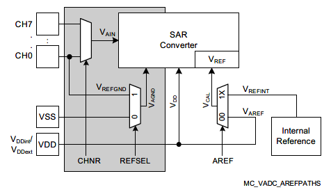
Figure 14. ADC Voltage Supply
Out of Range Comparator (ORC) Characteristics
The Out-of-Range Comparator (ORC) triggers on analog input voltages (
V
AIN
) above
V
DDP
on selected input pins (ORCx.AIN) and generates a service request trigger (ORCx.OUT).
Note:
These parameters are not subject to production test, but verified by design and/or characterization.
Parameter | Symbol | Values | Unit | Note/Test Condition | ||
|---|---|---|---|---|---|---|
Min. | Typ. | Max. | ||||
DC Switching Level | V ODC CC | – | – | 180 | mV | V AIN ≥ V DDP + V ODC |
Hysteresis | V OHYS CC | 15 | – | 54 | mV | |
Always detected Overvoltage Pulse | t OPDD CC | 103 | – | – | ns | V AIN ≥ V DDP + 150 mV |
88 | – | – | ns | V AIN ≥ V DDP + 350 mV | ||
Never detected Overvoltage Pulse | t OPDN CC | – | – | 21 | ns | V AIN ≥ V DDP + 150 mV |
– | – | 11 | ns | V AIN ≥ V DDP + 350 mV | ||
Detection Delay | t ODD CC | 39 | – | 132 | ns | V AIN ≥ V DDP + 150 mV |
31 | – | 121 | ns | V AIN ≥ V DDP + 350 mV | ||
Release Delay | t ORD CC | 44 | – | 240 | ns | V AIN ≤ V DDP ; V DDP = 5 V |
57 | – | 340 | ns | V AIN ≤ V DDP ; V DDP = 3.3 V | ||
Enable Delay | t OED CC | – | – | 300 | ns | ORCCTRL.ENORCx = 1 |
Figure 15. ORCx.OUT Trigger Generation
Figure 16. ORC Detection Ranges
Analog Comparator Characteristics
below shows the Analog Comparator characteristics.
Note:
These parameters are not subject to production test, but verified by design and/or characterization.
Parameter | Symbol | Limit Values | Unit | Note/Test Condition | |||
|---|---|---|---|---|---|---|---|
Min. | Typ. | Max. | |||||
Input Voltage | V CMP SR | -0.05 | – | V DDP + 0.05 | V | ||
Input Offset | V CMPOFF CC | – | +/-3 | – | mV | High power mode Δ V CMP < 200 mV | |
Propagation Delay | t PDELAY CC | – | 25 | – | ns | High power mode, Δ V CMP = 100 mV | |
– | 80 | – | ns | High power mode, Δ V CMP = 25 mV | |||
– | 250 | – | ns | Low power mode, Δ V CMP = 100 mV | |||
– | 700 | – | ns | Low power mode, Δ V CMP = 25 mV | |||
Current Consumption | I ACMP CC | – | 100 | – | µA | First active ACMP in high power mode, Δ V CMP > 30 mV | |
– | 66 | – | µA | Each additional ACMP in high power mode, Δ V CMP > 30 mV | |||
– | 10 | – | µA | First active ACMP in low power mode | |||
– | 6 | – | µA | Each additional ACMP in low power mode | |||
Input Hysteresis | V HYS CC | – | +/-15 | – | mV | ||
Filter Delay 21 | t FDELAY CC | – | 5 | – | ns | ||
Temperature Sensor Characteristics
Note:
These parameters are not subject to production test, but verified by design and/or characterization.
Parameter | Symbol | Values | Unit | Note/Test Condition | ||
|---|---|---|---|---|---|---|
Min. | Typ. | Max. | ||||
Measurement time | t M CC | – | – | 10 | ms | |
Temperature sensor range | T SR SR | -40 | – | 115 | °C | |
Sensor Accuracy 22 | T TSAL CC | -6 | – | 6 | °C | T J > 20°C |
-10 | – | 10 | °C | 0°C ≤ T J ≤ 20°C | ||
– | -/+8 | – | °C | T J < 0°C | ||
Start-up time | t TSST SR | – | – | 15 | µs | |
Oscillator Pins
Note:
It is strongly recommended to measure the oscillation allowance (negative resistance) in the final target system (layout) to determine the optimal parameters for the oscillator operation. Please refer to the limits specified by the crystal or ceramic resonator supplier.
Note:
These parameters are not subject to production test, but verified
by design and/or characterization.
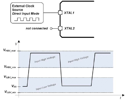
The oscillator pins can be operated with an external crystal/resonator (see
Figure 17
) or in direct input mode (see
Figure 18
).
Figure 17. Oscillator in Crystal Mode
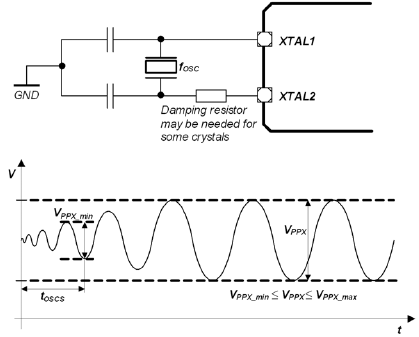
Figure 18. Oscillator in Direct Input Mode
Parameter | Symbol | Values | Unit | Note/Test Condition | ||
|---|---|---|---|---|---|---|
Min. | Typ. | Max. | ||||
Input frequency | f OSC SR | 4 | − | 48 | MHz | Direct Input Mode |
4 | − | 20 | MHz | External Crystal Mode | ||
Oscillator start-up time 23 | t OSCS CC | − | − | 10 | ms | |
Input voltage at XTAL1 | V IX SR | -0.3 | − | 1.5 | V | External Crystal Mode |
-0.3 | − | 5.5 | V | Direct Input Mode | ||
Input amplitude (peak- to-peak) at XTAL1 24 25 | V PPX SR | 0.6 | − | 1.7 | V | External Crystal Mode |
Parameter | Symbol | Values | Unit | Note/Test Condition | ||
|---|---|---|---|---|---|---|
Min. | Typ. | Max. | ||||
Input frequency | f OSC SR | – | 32.768 | – | kHz | |
Oscillator start-up time 26 | t OSCS CC | – | – | 5 | s | |
Input voltage at RTC_XTAL1 | V IX SR | -0.3 | – | 1.5 | V | |
Input amplitude (peak- to-peak) at RTC_XTAL1 27 28 | V PPX SR | 0.2 | – | 1.2 | V | |
Power Supply Current
The total power supply current defined below consists of a leakage and a switching component.
Application relevant values are typically lower than those given in the following tables, and depend on the customer's system operating conditions (e.g. thermal connection or used application configurations).
Note:
These parameters are not subject to production test, but verified by design and/or characterization.
Parameter | Symbol | Values | Unit | Note/Test Condition | ||
|---|---|---|---|---|---|---|
Min. | Typ. 29 | Max. | ||||
Active mode current Peripherals enabled f MCLK / f PCLK in MHz 30 | I DDPAE CC | – | 14.1 | 20 | mA | 48/96 |
– | 9.8 | – | mA | 24/48 | ||
– | 7.8 | – | mA | 16/32 | ||
– | 6.4 | – | mA | 8/16 | ||
– | 4.4 | – | mA | 1/1 | ||
Active mode current Peripherals disabled f MCLK / f PCLK in MHz 31 | I DDPAD CC | – | 6.2 | – | mA | 48/96 |
– | 4.6 | – | mA | 24/48 | ||
– | 3.6 | – | mA | 16/32 | ||
– | 3.1 | – | mA | 8/16 | ||
– | 1.8 | – | mA | 1/1 | ||
Active mode current Code execution from RAM Flash is powered down f MCLK / f PCLK in MHz | I DDPAR CC | – | 9.6 | – | mA | 48/96 |
Sleep mode current Peripherals clock enabled f MCLK / f PCLK in MHz 32 | I DDPSE CC | – | 11.0 | – | mA | 48/96 |
– | 7.6 | – | mA | 24/48 | ||
– | 6.4 | – | mA | 16/32 | ||
– | 5.3 | – | mA | 8/16 | ||
– | 4.2 | – | mA | 1/1 | ||
Sleep mode current Peripherals clock disabled Flash active f MCLK / f PCLK in MHz 33 | I DDPSD CC | – | 2.8 | – | mA | 48/96 |
– | 2.2 | – | mA | 24/48 | ||
– | 2.0 | – | mA | 16/32 | ||
– | 1.9 | – | mA | 8/16 | ||
– | 1.7 | – | mA | 1/1 | ||
Sleep mode current Peripherals clock disabled Flash powered down f MCLK / f PCLK in MHz 34 | I DDPSR CC | – | 2.2 | – | mA | 48/96 |
– | 1.7 | – | mA | 24/48 | ||
– | 1.4 | – | mA | 16/32 | ||
– | 1.2 | – | mA | 8/16 | ||
– | 1.1 | – | mA | 1/1 | ||
Deep Sleep mode current 35 | I DDPDS CC | – | 0.27 | – | mA | |
Wake-up time from Sleep to Active mode 36 | t SSA CC | – | 6 | – | cycles | |
Wake-up time from Deep Sleep to Active mode 37 | t DSA CC | – | 290 | – | µsec | |
shows typical graphs for active mode supply current for
V
DDP
= 5 V,
V
DDP
= 3.3 V,
V
DDP
= 1.8 V across different clock frequencies.
Figure 19. Active mode, a) peripherals clocks enabled, b) peripherals clocks disabled: Supply current I DDPA over supply voltage VDDP for different clock frequencies
shows typical graphs for sleep mode current for
V
DDP
= 5 V,
V
DDP
= 3.3 V,
V
DDP
= 1.8 V across different clock frequencies.
Figure 20. Sleep mode, peripherals clocks disabled, Flash powered down: Supply current IDDPSD over supply voltage VDDPfor different clock frequencies
provides the active current consumption of some modules operating at 5 V power supply at 25°C. The typical values shown are used as a reference guide on the current consumption when these modules are enabled.
Active Current Consumption | Symbol | Limit Values | Unit | Note/Test Condition |
|---|---|---|---|---|
Typ. | ||||
Baseload current | I CPUDDC | 4.14 | mA | Modules including Core, SCU, PORT, memories, ANATOP 38 |
VADC and SHS | I ADCDDC | 3.73 | mA | Set CGATCLR0.VADC to 1 39 |
USICx | I USIC0DDC | 1.35 | mA | Set CGATCLR0.USIC0 to 1 40 |
CCU4x | I CCU40DDC | 0.99 | mA | Set CGATCLR0.CCU40 to 1 41 |
CCU8x | I CCU80DDC | 1.00 | mA | Set CGATCLR0.CCU80 to 1 42 |
POSIFx | I PIF0DDC | 1.05 | mA | Set CGATCLR0.POSIF0 to 1 43 |
LEDTSx | I LTSxDDC | 1.14 | mA | Set CGATCLR0.LEDTSx to 1 44 |
BCCU0 | I BCCU0DDC | 0.29 | mA | Set CGATCLR0.BCCU0 to 1 45 |
MATH | I MATHDDC | 0.50 | mA | Set CGATCLR0.MATH to 1 46 |
WDT | I WDTDDC | 0.03 | mA | Set CGATCLR0.WDT to 1 47 |
RTC | I RTCDDC | 0.01 | mA | Set CGATCLR0.RTC to 1 48 |
MultiCAN | I MCANDDC | 1.38 | mA | Set CGATCLR0.MCAN0 to 1 49 |
Flash Memory Parameters
Note:
These parameters are not subject to production test, but verified by design and/or characterization.
Parameter | Symbol | Values | Unit | Note/Test Condition | ||
|---|---|---|---|---|---|---|
Min. | Typ. | Max. | ||||
Erase time per page/sector | t ERASE CC | 6.8 | 7.1 | 7.6 | ms | |
Program time per block | t PSER CC | 102 | 152 | 204 | µs | |
Wake-Up time | t WU CC | – | 32.2 | – | µs | |
Read time per word | t a CC | – | 50 | – | ns | |
Data Retention Time | t RET CC | 10 | – | – | years | Max. 100 erase/program cycles |
Flash Wait States 50 | N WSFLASH CC | 0 | 0 | 0 | f MCLK = 8 MHz | |
0 | 1 | 1 | f MCLK = 16 MHz | |||
1 | 2 | 2 | f MCLK = 32 MHz | |||
2 | 2 | 3 | f MCLK = 48 MHz | |||
Erase Cycles | N ECYC CC | – | – | 5*10 4 | cycles | Sum of page and sector erase cycles |
Total Erase Cycles | N TECYC CC | – | – | 2*10 6 | cycles | |
Figure 21.
Logical Structure of the Flash
AC Parameters
Testing Waveforms
Figure 22. Rise/Fall Time Parameters
Figure 23. Testing Waveform, Output Delay
Figure 24. Testing Waveform, Output High Impedance
Power-Up and Supply Threshold Characteristics
provides the characteristics of the supply threshold in XMC1400.
The guard band between the lowest valid operating voltage and the brownout reset threshold provides a margin for noise immunity and hysteresis. The electrical parameters may be violated while
V
DDP
is outside its operating range.
The brownout detection triggers a reset within the defined range. The prewarning detection can be used to trigger an early warning and issue corrective and/or fail-safe actions in case of a critical supply voltage drop.
Note:
These parameters are not subject to production test, but verified by design and/or characterization.
Parameter | Symbol | Values | Unit | Note/Test Condition | ||
|---|---|---|---|---|---|---|
Min. | Typ. | Max. | ||||
V DDP ramp-up time | t RAMPUP SR | V DDP / S VDDPrise | – | 10 7 | µs | |
V DDP slew rate | S VDDPOP SR | 0 | – | 0.1 | V/µs | Slope during normal operation |
S VDDP10 SR | 0 | – | 10 | V/µs | Slope during fast transient within +/-10% of V DDP | |
S VDDPrise SR | 0 | – | 10 | V/µs | Slope during power-on or restart after brownout event | |
S VDDPfall 51 SR | 0 | – | 0.25 | V/µs | Slope during supply falling out of the +/-10% limits 52 | |
V DDP prewarning voltage | V DDPPW CC | 2.1 | 2.25 | 2.4 | V | ANAVDEL.VDEL_SELECT = 00 |
2.85 | 3 | 3.15 | V | ANAVDEL.VDEL_SELECT = 01 | ||
4.2 | 4.4 | 4.6 | V | ANAVDEL.VDEL_SELECT = 10 | ||
V DDP brownout reset voltage | V DDPBO CC | 1.55 | 1.62 | 1.75 | V | calibrated, before user code starts running |
V DDP voltage to ensure defined pad states | V DDPPA CC | – | 1.0 | – | V | |
Start-up time from power-on reset | t SSW SR | – | 260 | – | µs | Time to the first user code instruction 53 |
BMI program time | t BMI SR | – | 8.25 | – | ms | Time taken from a user-triggered system reset after BMI installation is requested |
Figure 25. Supply Threshold Parameters
On-Chip Oscillator Characteristics
provides the characteristics of the 96 MHz digital controlled oscillator DCO1.
Note:
These parameters are not subject to production test, but verified by design and/or characterization.
Parameter | Symbol | Limit Values | Unit | Note/Test Condition | ||
|---|---|---|---|---|---|---|
Min. | Typ. | Max. | ||||
Nominal frequency | f NOM CC | – | 96 | – | MHz | under nominal conditions 54 after trimming |
Accuracy with adjustment based on XTAL as reference | Δ f LTX CC | -0.3 | – | 0.3 | % | with respect to fNOM (typ), over temperature (-40°C to 105°C) |
Accuracy | Δ f LT CC | -1.7 | – | 3.4 | % | with respect to f NOM (typ), over temperature (0°C to 85°C) |
-3.9 | – | 4.0 | % | with respect to f NOM (typ), over temperature (-40°C to 105°C) | ||
provides the characteristics of the 32 kHz digital controlled oscillator DCO2.
Parameter | Symbol | Limit Values | Unit | Note/Test Condition | ||
|---|---|---|---|---|---|---|
Min. | Typ. | Max. | ||||
Nominal frequency | f NOM CC | – | 32.75 | – | kHz | under nominal conditions after trimming |
Accuracy | Δ f LT CC | -1.7 | – | 3.4 | % | with respect to f NOM (typ), over temperature (0°C to 85°C) |
-3.9 | – | 4.0 | % | with respect to f NOM (typ), over temperature (-40°C to 105°C) 55 | ||
Serial Wire Debug Port (SW-DP) Timing
The following parameters are applicable for communication through the SW-DP interface.
Note:
These parameters are not subject to production test, but verified by design and/or characterization.
Parameter | Symbol | Values | Unit | Note/Test Condition | ||
|---|---|---|---|---|---|---|
Min. | Typ. | Max. | ||||
SWDCLK high time | t 1 SR | 50 | – | 500000 | ns | – |
SWDCLK low time | t 2 SR | 50 | – | 500000 | ns | – |
SWDIO input setup to SWDCLK rising edge | t 3 SR | 10 | – | – | ns | – |
SWDIO input hold after SWDCLK rising edge | t 4 SR | 10 | – | – | ns | – |
SWDIO output valid time after SWDCLK rising edge | t 5 CC | – | – | 68 | ns | C L = 50 pF |
– | – | 62 | ns | C L = 30 pF | ||
SWDIO output hold time from SWDCLK rising edge | t 6 CC | 4 | – | – | ns | |
Figure 26. SWD Timing
SPD Timing Requirements
The optimum SPD decision time between
0
and
1
is 0.75 µs. With this value the system has maximum robustness against frequency deviations of the sampling clock on tool and on device side. However it is not always possible to exactly match this value with the given constraints for the sample clock. For instance for a oversampling rate of 4, the sample clock will be 8 MHz and in this case the closest possible effective decision time is 5.5 clock cycles (0.69 µs).
Sample Freq. | Sampling Factor | Sample Clocks 0 | Sample Clocks 1 | Effective Decision Time 56 | Remark |
|---|---|---|---|---|---|
8 MHz | 4 | 1 to 5 | 6 to 12 | 0.69 µs | The other closest option (0.81 µs) for the effective decision time is less robust. |
For a balanced distribution of the timing robustness of SPD between tool and device, the timing requirements for the tool are:
Frequency deviation of the sample clock is +/- 5%
Effective decision time is between 0.69 µs and 0.75 µs (calculated with nominal sample frequency)
Peripheral Timings
Note:
These parameters are not subject to production test, but verified by design and/or characterization.
Synchronous Serial Interface (USIC SSC) Timing
The following parameters are applicable for a USIC channel operated in SSC mode.
Note:
Operating Conditions apply.
Parameter | Symbol | Values | Unit | Note/Test Condition | ||
|---|---|---|---|---|---|---|
Min. | Typ. | Max. | ||||
SCLKOUT master clock period | t CLK CC | 4/ MCLK | – | – | ns | |
Slave select output SELO active to first SCLKOUT transmit edge | t 1 CC | t CLK /2 - 28 | – | – | ns | |
Slave select output SELO inactive after last SCLKOUT receive edge | t 2 CC | 0 | – | – | ns | |
Data output DOUT[3:0] valid time | t 3 CC | -28 | – | 28 | ns | |
Receive data input DX0/DX[5:3] setup time to SCLKOUT receive edge | t 4 SR | 75 | – | – | ns | |
Data input DX0/DX[5:3] hold time from SCLKOUT receive edge | t 5 SR | 0 | – | – | ns | |
Parameter | Symbol | Values | Unit | Note/Test Condition | ||
|---|---|---|---|---|---|---|
Min. | Typ. | Max. | ||||
DX1 slave clock period | t CLK SR | 4/ MCLK | – | – | ns | |
Select input DX2 setup to first clock input DX1 transmit edge | t 10 SR | 16 | – | – | ns | |
Select input DX2 hold after last clock input DX1 receive edge 57 | t 11 SR | 17 | – | – | ns | |
Receive data input DX0/DX[5:3] setup time to shift clock receive edge 57 | t 12 SR | 21 | – | – | ns | |
Data input DX0/DX[5:3] hold time from clock input DX1 receive edge 57 | t 13 SR | 15 | – | – | ns | |
Data output DOUT[3:0] valid time | t 14 CC | – | – | 71 | ns | |
Figure 27. USIC - SSC Master/Slave Mode Timing
Note:
This timing diagram shows a standard configuration, for which the slave select signal is low-active, and the serial clock signal is not shifted and not inverted.
Inter-IC (IIC) Interface Timing
The following parameters are applicable for a USIC channel operated in IIC mode.
Note:
Operating Conditions apply.
Parameter | Symbol | Values | Unit | Note/Test Condition | ||
|---|---|---|---|---|---|---|
Min. | Typ. | Max. | ||||
Fall time of both SDA and SCL | t 1 CC/SR | – | – | 300 | ns | |
Rise time of both SDA and SCL | t 2 CC/SR | – | – | 1000 | ns | |
Data hold time | t 3 CC/SR | 0 | – | – | µs | |
Data set-up time | t 4 CC/SR | 250 | – | – | ns | |
LOW period of SCL clock | t 5 CC/SR | 4.7 | – | – | µs | |
HIGH period of SCL clock | t 6 CC/SR | 4.0 | – | – | µs | |
Hold time for (repeated) START condition | t 7 CC/SR | 4.0 | – | – | µs | |
Set-up time for repeated START condition | t 8 CC/SR | 4.7 | – | – | µs | |
Set-up time for STOP condition | t 9 CC/SR | 4.0 | – | – | µs | |
Bus free time between a STOP and START condition | t 10 CC/SR | 4.7 | – | – | µs | |
Capacitive load for each bus line | C b SR | – | – | 400 | pF | |
Parameter | Symbol | Values | Unit | Note/Test Condition | ||
|---|---|---|---|---|---|---|
Min. | Typ. | Max. | ||||
Fall time of both SDA and SCL | t 1 CC/SR | 20 + 0.1* C b 60 | – | 300 | ns | |
Rise time of both SDA and SCL | t 2 CC/SR | 20 + 0.1* C b | – | 300 | ns | |
Data hold time | t 3 CC/SR | 0 | – | – | µs | |
Data set-up time | t 4 CC/SR | 100 | – | – | ns | |
LOW period of SCL clock | t 5 CC/SR | 1.3 | – | – | µs | |
HIGH period of SCL clock | t 6 CC/SR | 0.6 | – | – | µs | |
Hold time for (repeated) START condition | t 7 CC/SR | 0.6 | – | – | µs | |
Set-up time for repeated START condition | t 8 CC/SR | 0.6 | – | – | µs | |
Set-up time for STOP condition | t 9 CC/SR | 0.6 | – | – | µs | |
Bus free time between a STOP and START condition | t 10 CC/SR | 1.3 | – | – | µs | |
Capacitive load for each bus line | C b SR | – | – | 400 | pF | |
Figure 28. USIC IIC Timing
Inter-IC Sound (IIS) Interface Timing
The following parameters are applicable for a USIC channel operated in IIS mode.
Note:
Operating Conditions apply.
Parameter | Symbol | Values | Unit | Note/Test Condition | ||
|---|---|---|---|---|---|---|
Min. | Typ. | Max. | ||||
Clock period | t 1 CC | 4/ f MCLK | – | – | ns | |
Clock HIGH | t 2 CC | 0.35 × t 1min | – | – | ns | |
Clock Low | t 3 CC | 0.35 × t 1min | – | – | ns | |
Hold time | t 4 CC | 0 | – | – | ns | |
Clock rise time | t 5 CC | – | – | 0.15 × t 1min | ns | |
Figure 29. USIC IIS Master Transmitter Timing
Parameter | Symbol | Values | Unit | Note/Test Condition | ||
|---|---|---|---|---|---|---|
Min. | Typ. | Max. | ||||
Clock period | t 6 SR | 4/ f MCLK | – | – | ns | |
Clock HIGH | t 7 SR | 0.35 × t 6min | – | – | ns | |
Clock Low | t 8 SR | 0.35 × t 6min | – | – | ns | |
Set-up time | t 9 SR | 0.3 × t 6min | – | – | ns | |
Hold time | t 10 SR | 15 | – | – | ns | |
Figure 30. USIC IIS Slave Receiver Timing
Package and Reliability
The XMC1400 is a member of the XMC1000 Family of microcontrollers. It is also compatible to a certain extent with members of similar families or subfamilies.
Each package is optimized for the device it houses. Therefore, there may be slight differences between packages of the same pin-count but for different device types. In particular, the size of the exposed die pad may vary.
If different device types are considered or planned for an application, it must be ensured that the board layout fits all packages under consideration.
Package Parameters
provides the thermal characteristics of the packages used in XMC1400.
Parameter | Symbol | Limit Values | Unit | Package Types | |
|---|---|---|---|---|---|
Min. | Max. | ||||
Exposed Die Pad Dimensions | Ex × Ey CC | – | 3.7 × 3.7 | mm | PG-VQFN-40-17 |
– | 4.2 × 4.2 | mm | PG-VQFN-48-73 | ||
– | 4.6 × 4.6 | mm | PG-VQFN-64-6 | ||
Thermal resistance Junction-Ambient | R ΘJA CC | – | 86.0 | K/W | PG-TSSOP-38-9 |
– | 45.3 | K/W | PG-VQFN-40-17 61 | ||
– | 44.9 | K/W | PG-VQFN-48-73 61 | ||
– | 66.7 | K/W | PG-LQFP-64-26 61 | ||
– | 44.7 | K/W | PG-VQFN-64-6 61 | ||
– | TBD | K/W | PG-LQFP-48-10 | ||
Note:
For electrical reasons, it is required to connect the exposed pad to the board ground VSSP, independent of EMC and thermal requirements.
Thermal Considerations
When operating the XMC1400 in a system, the total heat generated in the chip must be dissipated to the ambient environment to prevent overheating and the resulting thermal damage.
The maximum heat that can be dissipated depends on the package and its integration into the target board. The “Thermal resistance
R
ΘJA
” quantifies these parameters. The power dissipation must be limited so that the average junction temperature does not exceed 115°C.
The difference between junction temperature and ambient temperature is determined by
Δ
T
= (
P
INT
+
P
IOSTAT
+
P
IODYN
) ×
R
ΘJA
The internal power consumption is defined as
P INT
=
V
DDP
×
I
DDP
(switching current and leakage current).
The static external power consumption caused by the output drivers is defined as
P IOSTAT
= Σ((
V
DDP
-
V
OH
) ×
I
OH
) + Σ(
V
OL
×
I
OL
)
The dynamic external power consumption caused by the output drivers (
P
IODYN
) depends on the capacitive load connected to the respective pins and their switching frequencies.
If the total power dissipation for a given system configuration exceeds the defined limit, countermeasures must be taken to ensure proper system operation:
Reduce
V
DDP
, if possible in the system
Reduce the system frequency
Reduce the number of output pins
Reduce the load on active output drivers
Package Outlines
Figure 31. PG-TSSOP-38-9
Figure 32. PG-VQFN-40-17
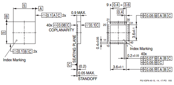
Figure 33. PG-VQFN-48-73
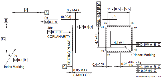
Figure 34. PG-VQFN-64-6
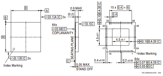
Figure 35. PG-LQFP-48-10
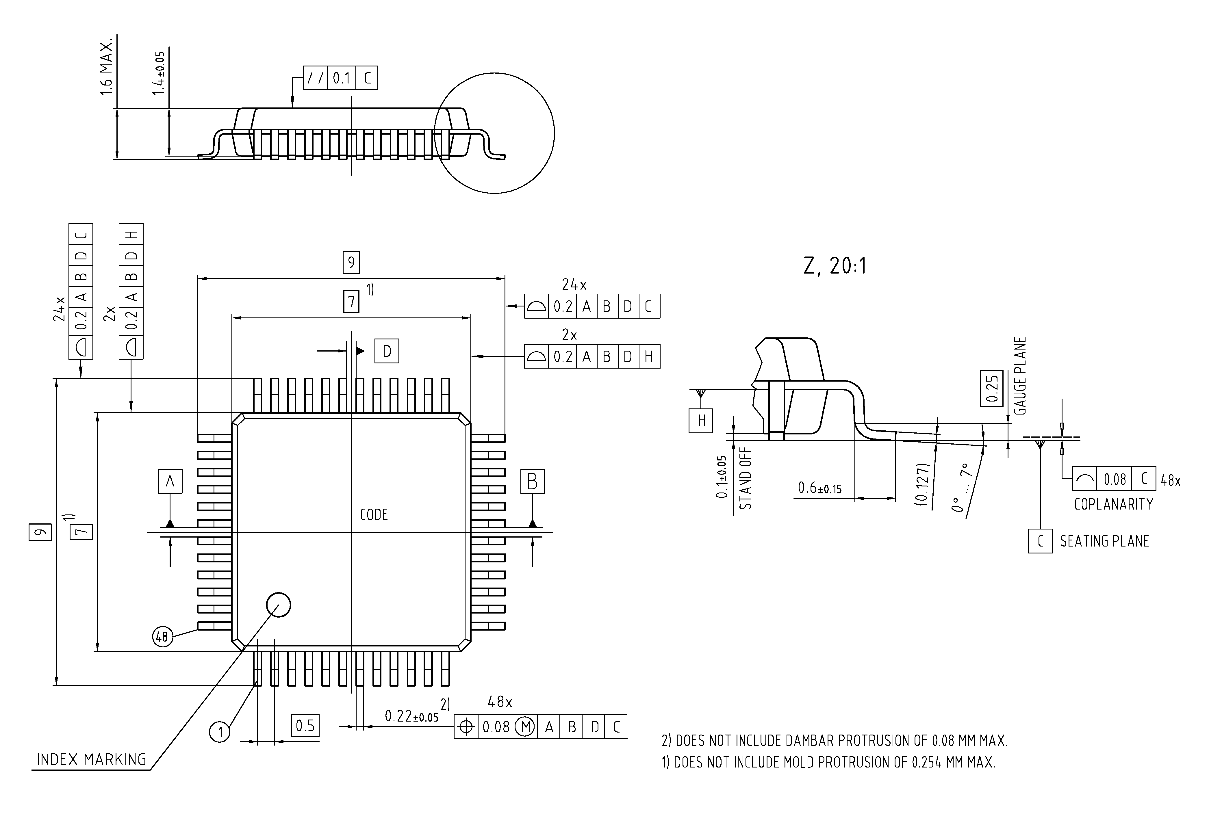
Figure 36. PG-LQFP-64-26
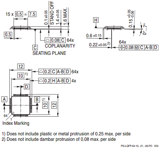
All dimensions in mm.
Quality Declaration
shows the characteristics of the quality parameters in the XMC1400.
Parameter | Symbol | Limit Values | Unit | Notes | |
|---|---|---|---|---|---|
Min. | Max. | ||||
ESD susceptibility according to Human Body Model (HBM) | V HBM SR | – | 4000 | V | Conforming to EIA/JESD22-A114-B |
ESD susceptibility according to Charged Device Model (CDM) pins | V CDM SR | – | 1000 | V | Conforming to JESD22-C101-C |
Moisture sensitivity level | MSL CC | – | – | – | JEDEC J-STD-020D |
| 3 | ||||
| 1 | ||||
| 3 | ||||
Soldering temperature | T SDR SR | – | 260 | °C | Profile according to JEDEC J-STD-020D |
Revision history
Document revision | Date | Description of changes |
|---|---|---|
V1.0 | 2016-02 | The device provides four USIC channels. XMC1401 devices available for max. ambient temperature of 85°C. Reformatted pinout table. Updated footnote to the definition of the start-up times of OSC_XTAL and RTC_XTAL oscillators. Added Δ f LT parameter to on-chip oscillators DCO1 and DCO2. Updated package outline drawings. |
V1.1 | 2016-06 | Added TSSOP-38-9 package Added XMC1402-T038 marking variants in TSSOP-38 Added XMC1403-Q040 marking variants |
V1.2 | 2016-08 | Added XMC™ trademark Added XMC1402-T038X0200, XMC1402-Q040X0200 and XMC1402-Q048X0200 marking variants |
V1.3 | 2016-10 | In Absolute Maximum Ratings renamed parameter V CM to V INP2 , as the limitation is related to most P2 pins, also if no ACMP is available. Clarified limit to pins P2.[1,2,6:9,11] in Overload specification. Corrected XMC1402-T038X0200 and XMC1402-Q048X0200 marking variants in Table 2 . |
V1.4 | 2017-11 | Added XMC1404-Q040 variants in Table 1 Added XMC1404-Q040 variants in Table 2 Added XMC1404-Q040 variants in Table 3 |
V1.5 | 2024-04 | Updated CHIP ID - 1 bit from 0 to 1 in Table 3 Release to web |
V1.6 | 2025-01-22 | Updated template. Removed Tools from Features section. Updated Moisture sensitivity level in Quality Declaration section. |
V1.7 | 2025-07-17 | Added XMC1401, XMC1402, XMC1404 in LQFP-48 package ( Table 1 , Table 2 , Table 3 , Table 5 , Figure 5 , Figure 10 , Figure 35 ). Added XMC1401 in TSSOP-38 package ( Table 1 , Table 2 , Table 3 ). Updated ESD ratings in Table 38 . |
1
Features that are not included in this table are available in all the derivatives.
2
Excluding port pins P2.[1,2,6,7,8,9,11].
3
Applicable to port pins P2.[1,2,6,7,8,9,11].
5
Rise/Fall time parameters are taken with 10% - 90% of supply.
6
Additional rise/fall time valid for
C
L
= 50 pF -
C
L
= 100 pF @ 0.150 ns/pF at 5 V supply voltage.
7
Additional rise/fall time valid for
C
L
= 50 pF -
C
L
= 100 pF @ 0.205 ns/pF at 3.3 V supply voltage.
8
Additional rise/fall time valid for
C
L
= 50 pF -
C
L
= 100 pF @ 0.445 ns/pF at 1.8 V supply voltage.
12
Hysteresis is implemented to avoid meta stable states and switching due to internal ground bounce. It cannot be guaranteed that it suppresses switching due to external system noise.
13
An additional error current (
I
INJ
) will flow if an overload current flows through an adjacent pin.
14
However, for applications with strict low power-down current requirements, it is mandatory that no active voltage source is supplied at any GPIO pin when
V
DDP
is powered off.
15
The parameters are defined for ADC clock frequencies
f
SH
= 32 MHz for the full supply range, and
f
SH
= 48 MHz at
V
DD_int
,
V
DD_ext
= 5 V. Usage of any other frequencies may affect the ADC performance.
16
The alternate reference ground connection is separate for each converter. This mode, therefore, provides the lowest noise impact.
17
No pending samples assumed, excluding sampling time and calibration.
18
Includes synchronization and calibration (average of gain and offset calibration).
19
This parameter can also be defined as an SNR value: SNR[dB] = 20 × log(
A
MAXeff
/
N
RMS
).
With
A
MAXeff
= 2
N
/2, SNR[dB] = 20 × log(2048/
N
RMS
) [N = 12].
N RMS
= 1.5 LSB12, therefore, equals SNR = 20 × log(2048/1.5) = 62.7 dB.
20
Includes error from the reference voltage.
21
Total Analog Comparator Delay is the sum of Propagation Delay and Filter Delay.
22
The temperature sensor accuracy is independent of the supply voltage.
23
t
OSCS
is defined from the moment the oscillator is enabled with SCU_ANAOSCHPCTRL.MODE until the oscillations reach an amplitude at XTAL1 of 0.9 *
V
PPX
.
24
The external oscillator circuitry must be optimized by the customer and checked for negative resistance and amplitude as recommended and specified by crystal suppliers.
25
If the shaper unit is enabled and not bypassed.
26
t
OSCS
is defined from the moment the oscillator is enabled by the user with SCU_ANAOSCLPCTRL.MODE until the oscillations reach an amplitude at RTC_XTAL1 of 0.9 *
V
PPX
.
27
The external oscillator circuitry must be optimized by the customer and checked for negative resistance and amplitude as recommended and specified by crystal suppliers.
28
If the shaper unit is enabled and not bypassed.
30
CPU and all peripherals clock enabled, Flash is in active mode.
31
CPU enabled, all peripherals clock disabled, Flash is in active mode.
32
CPU in sleep, all peripherals clock enabled and Flash is in active mode.
33
CPU in sleep, Flash is in active mode.
34
CPU in sleep, Flash is powered down and code executed from RAM after wake–up.
35
CPU in sleep, peripherals clock disabled, Flash is powered down and code executed from RAM after wake-up.
36
CPU in sleep, Flash is in active mode during sleep mode.
37
CPU in sleep, Flash is in powered down mode during deep sleep mode.
38
Baseload current is measured with device running in user mode, MCLK=PCLK=48 MHz, with an endless loop in the flash memory. The clock to the modules stated in CGATSTAT0 are gated.
39
Active current is measured with: module enabled, MCLK=48 MHz, running in auto-scan conversion mode.
40
Active current is measured with: module enabled, each of the 2 USIC channels sending alternate messages at 57.6 kbaud every 200 ms.
41
Active current is measured with: module enabled, MCLK=PCLK=48 MHz, 1 CCU4 slice for PWM switching at 20 kHz with duty cycle varying at 10%-90%, 1 CCU4 slice in capture mode for reading period and duty cycle.
42
Active current is measured with: module enabled, MCLK=PCLK=48 MHz, 3 CCU8 slices with PWM frequency at 20 kHz and a period match interrupt used to toggle duty cycle between 10% and 90%.
43
Active current is measured with: module enabled, MCLK=48 MHz, PCLK=96 MHz, hall sensor mode.
44
Active current is measured with: module enabled, MCLK=48 MHz, 1 LED column, 6 LED/TS lines, Pad Scheme A with large pad hysteresis config, time slice duration = 1.048 ms.
45
Active current is measured with: module enabled, MCLK=48 MHz, PCLK=96 MHz, FCLK=0.8 MHz, Normal mode (BCCU clock = FCLK/4), 4 BCCU Channels with packers enabled and 1 Dimming Engine, change color or dim every 1 s.
46
Active current is measured with: module enabled, MCLK=48 MHz, PCLK=96 MHz, tangent calculation in while loop; CORDIC circular rotation, no keep, autostart; 32-by-32 bit signed DIV, autostart, DVS right shift by 11.
47
Active current is measured with: module enabled, MCLK=48 MHz, time-out mode; WLB = 0, WUB = 0x00008000; WDT serviced every 1 s.
48
Active current is measured with: module enabled, MCLK=48 MHz, Periodic interrupt enabled.
49
Active current is measured with: module enabled, MCLK=48 MHz, running at 20 MHz baudrate generator, 1 node activated, 1 transmit and 1 receive object active.
50
Flash wait states are automatically inserted by the Flash module during memory read when needed. Typical values are calculated from the execution of the Dhrystone benchmark program.
51
A capacitor of at least 100 nF has to be added between
V
DDP
and
V
SSP
to fulfill the requirement as stated for this parameter.
52
Valid for a 100 nF buffer capacitor connected to supply pin where current from capacitor is forwarded only to the chip. A larger capacitor value has to be chosen if the power source sink a current.
53
This values does not include the ramp-up time. During start-up firmware execution, MCLK is running at 48 MHz and the clocks to peripheral as specified in register CGATSTAT0 are gated.
57
These input timings are valid for asynchronous input signal handling of slave select input, shift clock input, and receive data input (bits DXnCR.DSEN = 0).
58
Due to the wired-AND configuration of an IIC bus system, the port drivers of the SCL and SDA signal lines need to operate in open-drain mode. The high level on these lines must be held by an external pull-up device, approximately 10 kOhm for operation at 100 kbit/s, approximately 2 kOhm for operation at 400 kbit/s.
59
Due to the wired-AND configuration of an IIC bus system, the port drivers of the SCL and SDA signal lines need to operate in open-drain mode. The high level on these lines must be held by an external pull-up device, approximately 10 kOhm for operation at 100 kbit/s, approximately 2 kOhm for operation at 400 kbit/s.
61
Device mounted on a 4-layer JEDEC board (JESD 51-5); exposed pad soldered.