PSOC™ Control C3 MCU
Programming specification
About this document
Scope and purpose
This document provides the information necessary to acquire the
PSOC™
Control C3 MCU family. It describes the communication protocol required for access by an external programmer, explains the acquisition algorithm, and gives a basic description of the physical connection. Pin locations and the electrical and timing specifications of the physical connection are not a part of this document: they can be found in the device datasheet. The programming algorithms described in the following sections are compatible with all
PSOC™
Control C3 MCUs.
Intended audience
This document is intended for anyone who wants to program PSOC™ Control C3 MCUs.
Introduction
This document provides the information necessary to acquire the
PSOC™
Control C3 MCU family. It describes the communication protocol required for access by an external programmer, explains the acquisition algorithm, and gives a basic description of the physical connection. Pin locations and the electrical and timing specifications of the physical connection are not a part of this document: They can be found in the device datasheet. The programming algorithms described in the following sections are compatible with all
PSOC™
Control C3 MCUs.
Programmer
Figure 1.
Programmer in development environment
In the manufacturing environment, the integrated development environment (IDE) block is absent because its main purpose is to produce a binary file (hex, elf, etc.). The programmer performs three functions:
Parses the binary file and extracts the necessary information
Interfaces with the silicon as a Serial Wire Debug (SWD) or JTAG master
Implements the programming algorithm by translating the data from binary file into SWD or JTAG signals
The structure of the programmer depends on its requirements. It can be software- or firmware-centric.
In a software-centric structure, the programmer’s hardware works as a bridge between the protocol (such as USB) and SWD or JTAG. An external device (software) passes all SWD/JTAG commands to the hardware through the protocol. The bridge is not involved in parsing the binary file and programming algorithm. This is the task of the upper layer (software). Examples of such programmers are MiniProg4 and Segger J-Link.
A firmware-centric structure is an independent hardware design in which all the functions of the programmer are implemented in one device, including storage for the binary file. Its main purpose is to act as a mass programmer in manufacturing.
This document does not discuss the specific implementation of the programmer. It focuses on data flow, algorithms, and physical interfacing.
PSOC Control C3 MCU family overview
The
PSOC™
Control C3 MCU family is a single-CPU utilizing the Arm® Cortex®-M33 processor core. This MCU family supports the Arm® SWJ-DP interface for programming and debugging operations, using SWD or JTAG protocols.
This document includes the following appendices:
Appendix A: Intel hex file format
Appendix B: Serial wire debug (SWD) protocol
Appendix C: Joint Test Action Group (JTAG) protocol
Appendix D: Code example
Note: JTAG for PSOC™ Control C3 is available if the respective configuration is set in the provisioning policy.
Nonvolatile memory subsystem
Internal flash
The size of the flash memory varies depending on the target. A type of the flash is NOR. A target has flash, Sflash with secure/non-secure aliases to conform to an Arm® TrustZone feature. Also, there are S-bus (read and write) and C-bus (read and execute) aliases. Offsets of flash aliases are shown in
Table 1
. Each macro presented in a target consists of an integer. A programmer writes one row at a time. The number of rows varies based on the size of the flash memory. A size of a row for the
PSOC™
Control C3 MCU is 512 bytes.
PSOC™
Control C3 MCU does not have user Sflash, which means that Sflash cannot be used to store user data.
Memory | Non-secure C-bus | Secure C-bus | Non-secure S-bus | Secure S-bus |
|---|---|---|---|---|
SFLASH | 0x03400000 | 0x13400000 | 0x23400000 | 0x33400000 |
FLASH | 0x02000000 | 0x12000000 | 0x22000000 | 0x32000000 |
Also, flash memory can have row and chip level protections, refresh features, and a defined implementation. A typical flash memory structure is as shown in Figure 2.
Figure 2. Typical flash memory structure
Internal flash is programmed via SROM APIs. All these functions are blocking; that is, a processor exits only when a function is done. Pointers to necessary functions are shown in Table 2. The actual function pointer is stored at a given address.
Address | Function pointer |
|---|---|
0x1080FFE8u | cyboot_flash_write_row |
0x1080FFE4u | cyboot_flash_program_row |
0x1080FFE0u | cyboot_flash_erase_row |
Note: If image to be flashed contains C-bus addresses, redirect this data to S-bus alias as it is done in official programming tools.
Dual bank mode
PSOC™
Control C3 MCU has a dual bank mode feature. This feature divides both secure and non-secure flash banks into two parts, and second part of it has an offset of 0x800000. For example, in dual bank mode, secure flash bank is divided into:
bank 0 - 0x32000000
bank 1 - 0x32800000
New banks are half the size of the original bank. This feature relates to both S- and C- bus, but has nothing to do with SFlash.
To reprovision to single/dual-bank mode many times, use the Edge Protect Tools.
Hex file
This chapter describes the information that the programmer must extract from the hex file to program the
PSOC™
Control C3 MCU.
Organization of the hex file
The hexadecimal (hex) file describes the nonvolatile configuration of the project. It is the data source for the programmer.
The hex file for the
PSOC™
Control C3 MCU follows the Intel hex file format. Intel’s specification is very generic and defines only some types of records that can make up the hex file. The specification allows customizing the format for any possible silicon architecture. The silicon vendor defines the functional meaning of the records, which typically varies for different chip families. See
Appendix A: Intel hex file format
for details of the Intel hex file format.
The protocol stack
This chapter explains the low-level details of the communication interface.
Figure 3
illustrates the stack of protocols involved in the programming process. The programmer must implement both hardware and software components.
Figure 3. Programmer’s protocol stack
The programming algorithm protocol, the topmost protocol, implements the whole programming flow in terms of logical and algorithmic steps. This protocol is implemented completely in software. Its smallest building block is the SWD or JTAG command. The whole programming algorithm is the meaningful flow of these blocks
The communication interface layer acts as a bridge between pure software and hardware implementations. SWJ interface implements a set of lower-level (protocol-dependent) commands. It also transforms the software representation of these commands into line signals (digital form). The SWJ interface helps to isolate the programming algorithm from hardware specifics, which makes the algorithm reusable
The physical layer is the complete hardware specification of the signals and interfacing pins and includes drive modes, voltage levels, resistance, and other components
Communication interface
The external device (whether it is Infineon-supplied programmer and debugger or a third-party device that supports programming and debugging) can access most internal resources through the “Program and debug” interface provided in
PSOC™
Control C3 MCU silicon. The SWD or the JTAG interface can be used as the communication protocol between the external device and the
PSOC™
Control C3 MCU.
Program and debug interface
The main purpose of
PSOC™
Control C3 MCU program and debug interface is to support programming and debugging through the JTAG or SWD interface and to provide read and write access to all memory and registers in the system while debugging, including the Cortex®-M33 register banks when the core is running or halted.
The
PSOC™
Control C3 MCU silicon implements a DAP, which integrates SWJ-DP (serial wire/JTAG debug port) and complies with the Arm® specification “Arm® debug interface architecture specification ADIv6.0 (Arm® IHI 0074D)”.
The debug physical port pins communicate with the DAP through the high-speed I/O matrix (HSIOM). The DAP communicates with the Cortex®-M33 CPU using the Arm®-specified advanced high-performance bus (AHB) interface. AHB is the system’s interconnect protocol used inside the device, which facilitates memory and peripheral register access by the AHB master. The
PSOC™
Control C3 MCU has several AHB masters, including the Arm® CM33 CPU core and DAP. The external host can effectively take control of the entire device through the DAP to perform programming and debugging operations.
The debug port (DP) connects to the DAP bus, which in turn connects to one of two access ports (AP), namely:
The CM33-AP: Located inside the CM33 core, gives access to the CM33 internal debug components. The CM33-AP port also allows access to the rest of the system through the CM33 AHB master interfaces. This provides the debug host the same view as an application running on the CM33 core
The System-AP: Gives access to the rest of the system. This allows access to the system ROM table, which is not intended to be reached any other way. The system ROM table provides the MCU ID
DAP power domain
Almost all the debug components are part of the active power domain. The only exception is the SWD/JTAG-DP, which is part of the Deep-Sleep power domain. This allows the debug host to connect during Deep-Sleep mode, while the application is 'running' or powered down. This enables infield debugging for low-power applications in which the chip is mostly in Deep-Sleep mode.
After the debugger is connected to the chip, it must bring the chip to the active state before any operation. For this, the SWD/JTAG-DP has a register (DP_CTL_STAT) with two power request bits. The two bits are:
CDBGPWRUPREQ: Requests for debug power
CSYSPWRUPREQ: Requests for system power
These bits must remain set for the duration of the debug session.
Note: Only the two SWD pins (SWCLKTCK and SWDIOTMS) are operational during the Deep-Sleep mode – the JTAG pins are operational only in active mode. The JTAG debug and JTAG boundary scan are not available when the system is in Deep-Sleep mode.
SWD/JTAG selection
JTAG and SWD are mutually exclusive because of the Arm® SWJ-DP implementation and because they share pins. Therefore, an external programmer/debugger must be able to switch to the required protocol. The watcher circuit, implemented in SWJ-DP, detects a specific 16-bit select sequence on SWDIOTMS and determines whether the JTAG or SWD interface is active. By default, JTAG operations are selected on power-on reset and therefore, the JTAG protocol can be used from reset without sending a select sequence. The protocol switching can only occur when the selected interface is in its reset state (test-logic-reset for JTAG and line-reset for SWD).
To switch SWJ-DP from JTAG to SWD operation:
Send at least 50 SWCLKTCK cycles with SWDIOTMS HIGH. This ensures that the current interface is in its reset state. The JTAG interface detects only the 16-bit JTAG-to-SWD sequence starting from the test-logic-reset state
Send the 16-bit JTAG-to-SWD select sequence on SWDIOTMS: 0b0111 1001 1110 0111, most significant bit (MSB) first. This can be represented as 0x79E7, transmitted MSB first or 0xE79E, transmitted least significant bit (LSB) first
Send at least 50 SWCLKTCK cycles with SWDIOTMS HIGH. This ensures that if SWJ-DP was already in SWD operation before sending the select sequence, the SWD interface enters line reset state
Figure 4. JTAG-to-SWD sequence timing
To switch SWJ-DP from SWD to JTAG operation:
Send at least 50 SWCLKTCK cycles with SWDIOTMS HIGH. This ensures that the current interface is in its reset state. The SWD interface detects the 16-bit SWD-to-JTAG sequence only when it is in reset state
Send the 16-bit SWD-to-JTAG select sequence on SWDIOTMS: 0b0011 1100 1110 0111, MSB first. This can be represented as 0x3CE7, transmitted MSB first, or 0xE73C, transmitted LSB first
Send at least five SWCLKTCK cycles with SWDIOTMS HIGH. This ensures that if SWJ-DP was already in JTAG operation before sending the select sequence, the JTAG TAP enters the test-logic-reset state
Figure 5. SWD-to-JTAG sequence timing
For a more detailed description, see the “SWD and JTAG select mechanism” section in “Arm® debug interface architecture specification ADIv6.0”.
For information on the structure of the SWD read and write packets and their waveform on the bus, see Appendix B: Serial wire debug (SWD) protocol. For information on the structure of the JTAG, see Appendix C: Joint Test Action Group (JTAG) protocol.
The DAP functionally is split into two control units:
Debug port (DP) – is responsible for the physical connection to the programmer or debugger
Access port (AP) – provides the interface between the DAP module and one or more debug components (such as the Cortex®-M33 CPU)
The external programmer can access the registers of these access ports using the following bits in the SWJ packet:
APnDP – select access port (0 – DP, 1 - AP)
ADDR – 2-bit field addressing a register in the selected access port
The SWJ read/write commands are used to access these registers. They are the smallest transactions that can appear on the SWJ bus.
Table 3
shows the DAP registers that are used during programming.
Register | APnDP (1 bit) | Address (2-bit) | Access (R/W) | Full name |
|---|---|---|---|---|
IDCODE | 0 | 2’b00 | R | Identification code register |
ABORT | 0 | 2’b00 | W | AP ABORT register |
CTRL/STAT | 0 | 2’b01 | R/W | Control/status register |
SELECT | 0 | 2’b10 | W | AP select register |
RDBUFF | 0 | 2’b11 | R | Data buffer register |
CSW | 1 | 2’b00 | R/W | Control status/word register (CSW) |
TAR | 1 | 2’b01 | R/W | Transfer address register |
DRW | 1 | 2’b11 | R/W | Data read/write register |
For more information about these registers, see the Arm® debug interface architecture specification ADIv6.0.
Physical layer
This section summarizes the hardware connection between the programmer and the
PSOC™
Control C3 MCU for programming.
Figure 6
shows the generic connection between the
PSOC™
Control C3 MCU and the programmer. See
Table 4
for pins/signals description.
Check the device datasheet for the part’s package pins location, electrical, and timing specifications.
Figure 6. Connection schematic of the programmer
Pin | SWD | JTAG | Description | ||
|---|---|---|---|---|---|
Signal name | Mandatory | Signal name | Mandatory | ||
SWCLKTCLK | SWCLK (serial wire clock) | YES | TCLK (test clock) | YES | Data synchronization clock, driven by the host programmer/debugger. For SWD, the host should perform all read or write operations on the SWDIO line on the falling edge of SWDCK. The PSOC™ Control C3 MCU performs read or write operations on SWDIO on the rising edge of SWDCK. For JTAG, the host writes to the TMS and TDI pins of the PSOC™ Control C3 MCU on the falling edge of TCK and the PSOC™ Control C3 MCU reads data on its TMS and TDI lines on the rising edge of TCK. PSOC™ Control C3 MCU writes to its TDO line on the falling edge of TCK and the host reads from the TDO line of the PSOC™ Control C3 MCU on the rising edge of TCK. |
SWDIOTMS | SWDIO (serial wire data input/output) | YES | TMS (test mode select) | YES | SWDIO is a bidirectional data input/output signal. TMS is the JTAG test mode select signal, which is sampled at the rising edge of TCK to determine the next state. |
SWOTDO | SWO (serial wire output) | NO | TDO (test data out) | YES | SWO signal (also known as TRACESWO) is required for serial wire viewer (SWV) and not required for SWD programming. It provides real-time data trace information from the PSOC™ Control C3 MCU, via the SWO pin, while the CPU continues to run at full speed. Data trace via SWV is not available using the JTAG interface. TDO signal represents the data shifted out of the device’s test or programming logic and is valid on the falling edge of TCK when the internal state machine is in the correct state. |
TDI | TDI (Test Data In) | YES | TDI signal represents the data shifted into the device’s test or programming logic. It is sampled at the rising edge of TCK. | ||
XRES | XRES (External Reset) | NO | XRES (Reset) | NO 1 | External reset active LOW signal. The XRES is not related to the Arm® standard. It is used to reset the part as a first step in a programming flow. |
GND | GND (Ground) | YES | GND (Ground) | YES | Negative supply voltage (Ground) |
VDD | VDD (voltage drain drain) | NO 2 | VDD (voltage drain drain) | NO 1 | Positive supply voltage. The PSOC™ Control C3 MCU can be powered by external power supply or by programmer. |
You can program a chip in either reset (recommended) or power cycle mode. The mode affects only the first step - how to reset the part at the start of the programming flow. All other steps are the same.
Reset mode: To start programming, the host toggles the XRES line and then sends SWD/JTAG commands (see Hardware-specific subroutines section). The power on the PSOC™ Control C3 MCU board can be supplied by the host or by an external power adapter (the VDD line can be optional).
Power cycle mode: To start programming, the host powers on the PSOC™ Control C3 MCU and then starts sending the SW/JTAG commands. The XRES line is not used
The programmer should implement
PSOC™
Control C3 MCU acquisition in reset mode. It is also the only way to acquire the
PSOC™
Control C3 MCU if the board consumes too much current, which the programmer cannot supply. Power cycle mode support is optional and should be used only in the following conditions:
The third-party programmer does not implement the XRES line but can supply power to the PSOC™ Control C3 MCU
1 XRES pin is mandatory for "Reset" PSOC™ Control C3 MCU acquisition mode, but not used for "power cycle" mode.
2 VDD pin is mandatory for "power cycle" PSOC™ Control C3 MCU acquisition mode, where the programmer powers the PSOC™ Control C3 MCU and external power is not applied. For "reset" acquisition mode, the source of power supplier does not matter, so the pin is optional.
1
XRES pin is mandatory for "Reset"
PSOC™
Control C3 MCU acquisition mode, but not used for "power cycle" mode.
2
VDD pin is mandatory for "power cycle"
PSOC™
Control C3 MCU acquisition mode, where the programmer powers the
PSOC™
Control C3 MCU and external power is not applied. For "reset" acquisition mode, the source of power supplier does not matter, so the pin is optional.
Acquisition algorithm
This chapter describes in detail the programming flow of the
PSOC™
Control C3 MCU. It starts with a high-level description of the algorithm and then describes every step using pseudocode. All code is based on upper-level subroutines composed of atomic SWJ instructions.
Constants and subroutines used in the acquisition flow
The following algorithms rely on a few low-level, hardware-specific subroutines which must be implemented by the user. This section provides only a short overview of these functions.
See Hardware-specific backend functions for details.
Subroutine | Description |
|---|---|
IsJTAG() | Returns any non-zero value if the underlying transport is JTAG (zero for SWD) |
SetXRES(…) | Controls the logic level on the XRES (nSRST) pin - hard reset |
SetVoltage(…) | Controls the voltage supplied by the debug adapter to power the target MCU. This function is optional and should return an error if not implemented. |
SWJSequence(…) | Generates the given bit sequence on the SWDIO/TMS pin, used for JTAG->SWD and SWD->JTAG switching |
ReadDAP(…) WriteDAP(…) | Reads (or writes) data to the CoreSight registers |
SysSleepMs(…) | Delays the execution by the given number of milliseconds |
SysGetTimeMs() | Returns the number of milliseconds that have elapsed since some fixed time point in the past |
See Constants and static data used in code for a detailed list of constants used by the subroutines.
The programming flow includes some operations that are used in all steps. The execution flow of these subroutines is straightforward, so only a summary table is provided here.
See Appendix D: Code example for a detailed description.
Subroutine | Description | Example |
|---|---|---|
ClearStickyErrors() | Clears any sticky errors which could be left from previous sessions | |
DAP_HandshakeAndInit(…) | Performs a handshake and initializes the debug port | |
ReadMem(…) | Reads a 32-bit value from the memory address provided | |
WriteMem(…) | Writes a 32-bit value to the memory address provided | |
PollMem(…) | Polls for the expected bit-field value in the given register | |
ReadCoreReg(…) | Reads the Arm® core register, special-purpose register, or floating-point register | |
WriteCoreReg(…) | Writes the Arm® core register, special-purpose register, or floating-point register | |
HaltCPU() | Enables debug and halts the CPU using the DHCSR register | |
ResumeCPU() | Enables debug and resumes the CPU using the DHCSR register | |
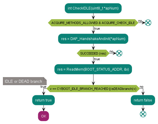
CheckIDLE(…) | Checks whether the device is in WFA (wait for action), IDLE or DEAD branches | |
AcquireTestMode(…) | Acquires target in test mode by setting the TST_MODE_TEST_MODE bit in the TST_MODE register | |
AcquireVectorCatch(…) | Acquires target using the vector catch method | |
WaitForWFAMode(…) | Waits for the boot code to enter WFA mode used in the unlock procedure using debug certificates | |
AcquireInWFAMode(…) | Acquires the device in WFA mode; used in the unlock procedure using debug certificates | |
LoadDebugCert(…) | Loads the debug certificate to the RAM; used in the unlock procedure using debug certificates | |
StartWFARequest(…) | Starts the WFA request; used in unlock procedure using debug certificates |
DAP initialization subroutines
The very first step required to initiate a connection between the debugger and the target MCU is to initialize the DAP port. This can be achieved by using the following subroutines:
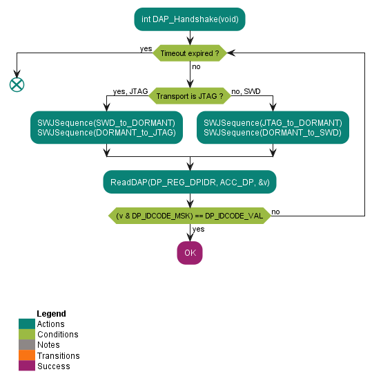
DAP_Handshake
Waits for the debug interface to become enabled after a device reset. Boot timing parameters are given in
Table 5
and are dependent on the CPU clock used by the boot code, type of boot, and other parameters. For PowerCycle acquisition, the timeout depends on the design schematic and must be longer.
See the code example provided in DAP_Handshake.
Figure 7. Flowchart of the DAP_Handshake subroutine
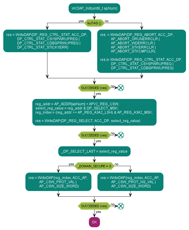
DAP_Init
Initializes the debug port for programing operations. DAP must be enabled and accessible at the moment this function is called.
Accepts access port number as the input:
0 – System AP
1 – CM33 AP
See the code example in DAP_Init.
Figure 8. Flowchart of the DAP_Init subroutine
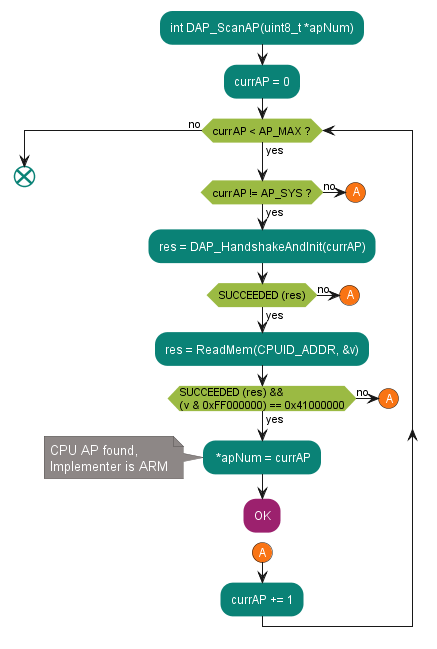
DAP_ScanAP
Scans the access ports first available with CPU registers access.
See the code example in
DAP_ScanAP
.
Figure 9. Flowchart of the DAP_ScanAP subroutine
Reset
The reset procedure is used during device acquisition; thus, it is very important for reset to reliably happen regardless of the state and hardware configuration of the target board. The most reliable reset type is hardware reset because it performs a full reset of the device including the reset of the retention registers which preserve their state between software resets.
The hardware reset signal can be routed to other (external to the MCU) peripherals on the target board. This ensures that all target systems start from the well-known state after reset.
Moreover, a hardware reset is required to perform the MCU acquisition in test mode, which is the recommended and most reliable acquisition method. It is strongly recommended to have the XRES pin properly routed to the debug connector.
If it is not possible for the debugger to perform a hardware reset for some reason (e.g., XRES signal not connected), the reset subroutine uses several strategies to ensure that the reset is successful. These include the following:
Hardware reset by toggling the XRES pin
Software reset by setting the RES_SOFT_CTL.TRIGGER_SOFT bit
Software reset by setting the AIRCR.SYSRESETREQ bit
Software reset by setting the DP->CTRL/STAT.CDBGRSTREQ bit
See the code example in
System reset
.
Figure 10. High-level flowchart of the reset procedure
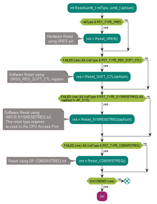
Figure 11. SOFT_RES_CTL reset
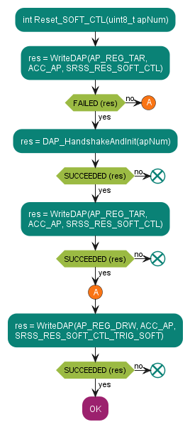
Figure 12. SYSRESETREQ reset
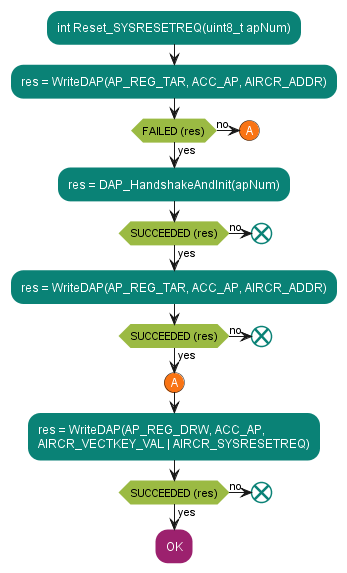
Figure 13. CDBGRSTREQ reset
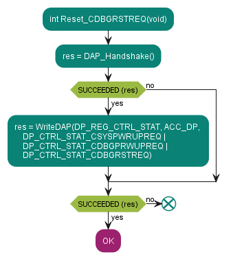
Acquire PSOC™ Control C3 MCU
The first step for the debugger before any programming or debugging actions is to acquire the device in a known good state and prevent execution of the user’s code, which can put the MCU into a bad or corrupted state or repurpose the SWJ pins 3.
There are five different steps for
PSOC™
Control C3 MCU acquiring, performed by the debugger sequentially:
Check the boot IDLE state
Acquire in test mode with hardware reset
Acquire in test mode with software reset
Acquire with vector catch with hardware reset
Acquire with vector catch with software reset
Figure 14. Top-level acquisition flowchart for PSOC™ Control C3 MCU
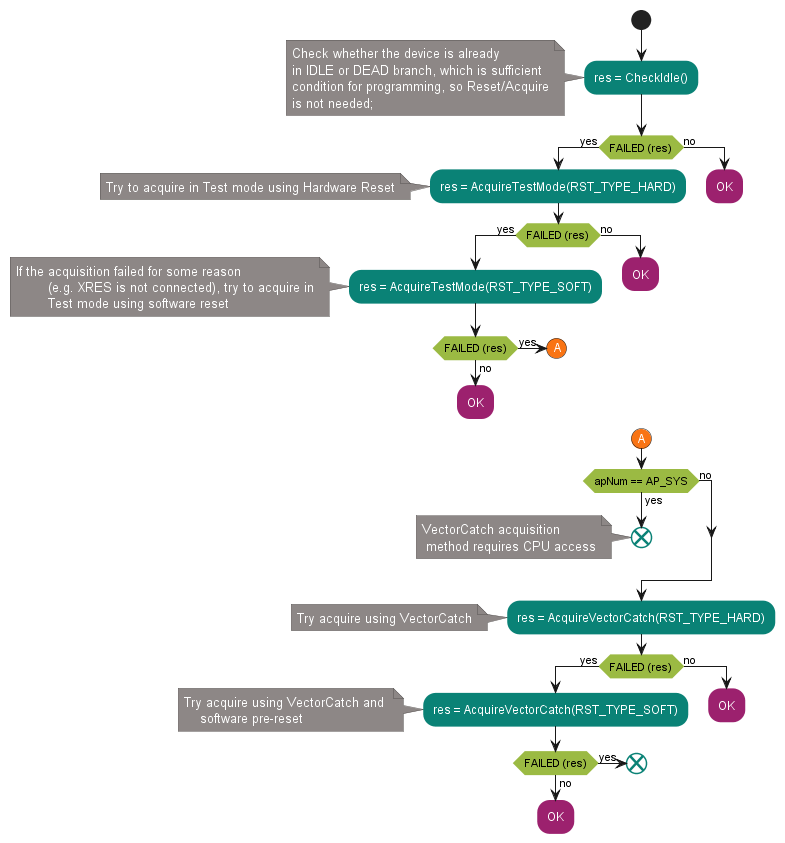
See the code example in AcquireVectorCatch.
Step 1 – check boot IDLE state
The IDLE state of the
PSOC™
Control C3 MCU is the state when the ROM boot code did not launch the user’s application, but is executing an endless loop in one of the following branches:
IDLE branch: The boot code entered test mode or waits for the debugger for further actions in preproduction lifecycle stages such as SORT, NORMAL, or RMA
DEAD branch: Indicates a recoverable failure occurred (for example, an invalid TOC object, an empty flash, or an invalid app inside)
CORRUPTED branch: Indicates that the major system failure occurred (for example, BIST failed), the debugger has limited MCU access (via system access port only), and the programming is not possible
IDLE and DEAD branches are sufficient MCU states for the debugger to perform further programming or debugging actions, so the additional device acquisition steps are not required.
Note: DEAD branch has many return codes.
Figure 15. Step 1 - check boot IDLE state flowchart
Step 2 – acquire in test mode
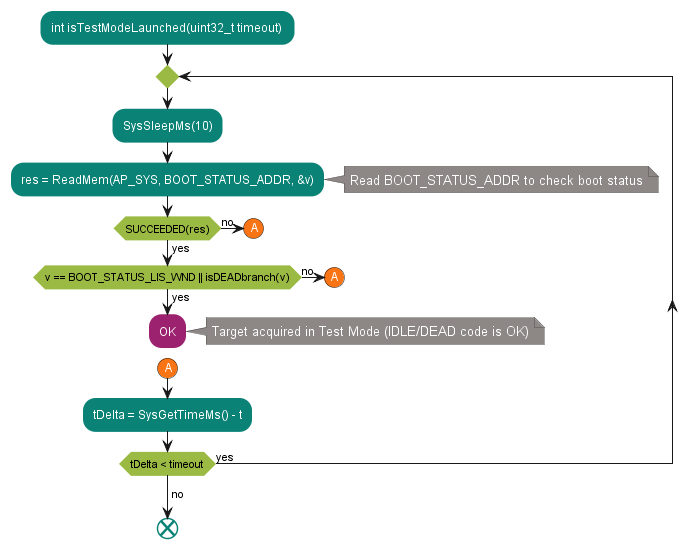
The test mode acquisition step has strict timing requirements that the host must meet to enter test mode successfully.
Figure 16. Timing diagram for entering test mode
This diagram details the chip’s internal signals while entering test mode. Everything starts from toggling the XRES line (or applying power) so that the chip enters internal reset mode for t
lite_up
period. After that, the system boot code starts execution. When completed, the CPU waits during a t
listen
period for a special connection sequence on the SWJ port. If, during this time, the host sends the correct sequence of SWJ commands, the CPU enters test mode. Otherwise, it starts the execution of the user’s code. Timing parameters may vary depending on the boot code execution flow (see
Table 5
). Therefore, the best way to enter test mode is to start sending an acquire sequence immediately after XRES is toggled (or power is supplied in power cycle mode). This sequence is sent iteratively until it succeeds (all SWJ transactions are ACKed and all conditions are met).
Parameter | Description | Min | Max | Units |
|---|---|---|---|---|
t lite_up | Time from reset release until the CPU begins executing the boot code | 250 | µs | |
t boot | Time from when the boot code started execution until it opens SWJ lines and starts waiting for the TEST_MODE sequence. This time varies depending on the CPU clock, device lifecycle stage, etc. Usually, less than 5 ms, but in the most harsh scenario, it can be up to 500 ms. | 2 | 500 | ms |
t listen | Amount of time the boot code waits and listens for the SWJ port initialization sequence before starting the application firmware execution. Note: The default duration of the listen window (tlisten) is 100 ms, but it may vary depending on the provisioning. | 0 | 100 | ms |
Figure 16 shows the test mode acquisition procedure. It is detailed in terms of the SWD transaction.
Figure 17. Test mode acquisition flowchart
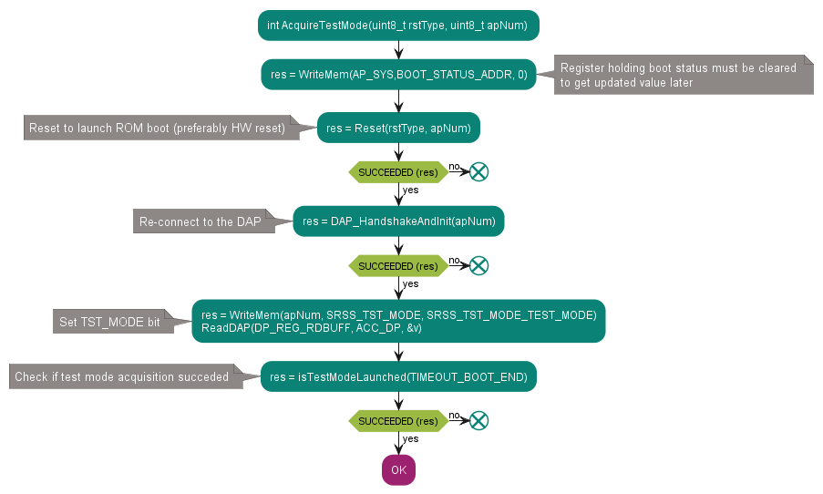
Figure 18. Flowchart for step 2 - acquire in test mode
See the code example in AcquireTestMode
Step 3 – acquire PSOC™ Control C3 MCU using vector catch
The “acquire chip” sequence in the previous section is based on entering the
PSOC™
Control C3 MCU test mode by triggering a hard-reset condition, and then sending the acquire sequence within the specified time window. The hard-reset condition is generated by toggling either the XRES pin or the power supply to the device. Programming by entering test mode using XRES or power cycling is the recommended method for third-party production programmers or any other general-purpose programmer.
There might be cases where the host programmer hardware or software constraints might prevent programming of the device in test mode. These constraints can include:
The host programmer hardware might be I/O-pin-constrained and cannot spare an extra I/O for toggling the XRES pin or the power supply to the MCU. Only the SWJ protocol pins are available for programming
The host programmer software application is unable to meet the timing requirements to enter test Mode after triggering a hard-reset condition. In such a scenario, the MCU enters the user code execution mode after the test mode timing window elapses
For a host programmer with any of these constraints, the modified acquire-chip sequence provided in this section does not require XRES/power supply toggling, and it does not have the test-mode timing requirements. Only the SWJ protocol pins are used for programming. This modified sequence works only under the following conditions:
The SWJ pins on the MCU have not been repurposed for any other application-firmware-specific use. If the SWJ pins are repurposed as part of the existing firmware image in the flash, the SWJ pins are not available for communication with the host SWJ interface to update the existing firmware image
The access restriction properties allow the SWJ access to the access debug ports (normal access restriction properties are applicable if the device is in the normal protection state, secure, and dead access restriction properties are applicable if the device is in the secure and dead protection states respectively)
Developers wanting to program devices using the modified sequence should be aware of these limitations. Devices coming from the factory satisfy both these conditions, and therefore, can be programmed using the modified acquire sequence. However, if firmware that does not meet any of these conditions, then the devices are programmed to the MCU, subsequent re-programming of the device is not possible using the modified acquire sequence. Due to this limitation, this method is not recommended for third-party programmers or general-purpose programmers because they would generally be required to support programming under all possible operating conditions.
Figure 19. Acquire using vector catch
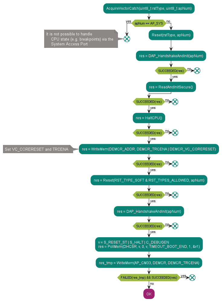
3
The application firmware is expected to follow this procedure for SWJ pin configuration:
Do not modify the configuration of the SWJ pins for parts that have a permanent SWD interface. They will be properly configured and may have already connected to the SWD probe when the firmware starts
For parts that repurpose their SWD pins:
If the SWD interface is presently active (CPUSS_DP_STATUS.SWJ_CONNECTED bit is ‘1’), leave the pins in their current state; a probe has connected during the acquire window and the pins should not be repurposed
If the SWD interface is not active, you may configure the pins and enable the alternate purpose
(use them as GPIO) such that the external debugger will not be able to communicate with the device.
Unlock the access to the CPU (helper functions)
The Cortex®-M33 access port can be disabled by the access restrictions policy. The access port can be either temporarily or permanently disabled. If temporarily disabled, it can be re-enabled using the debug certificate.
Note: Certificate cannot override the access port that is permanently disabled by access restrictions.
The Boot ROM verifies the certificate; if the verification is successful, it enables CM33-AP as specified in the certificate.
Procedure of opening CM33-AP using debug certificate:
RAM: Sys-AP must be enabled to load the debug certificate directly into the RAM which is reserved by Boot ROM at the end of RAM. This flow can be used to debug CM33 core. Flow details:
The debugger sets the appropriate BOOT_DLM_CTL.REQUEST and issues a software reset by setting RES_SOFT_CTL.TRIG_SOFT = 1
The Boot ROM resets, detects BOOT_DLM_CTL.REQUEST, and sets BOOT_DLM_CTL.WFA, thus, indicating that it waits for a certificate loaded
The debugger loads the debug certificate into the RAM using Sys-AP. The address of the certificate loaded must be placed at BOOT_DLM_CTL_2. After all, the debugger sets BOOT_DLM_CTL.REQUEST again to trigger the verifying certificate
Boot ROM can now verify the debug certificate
If verification is successful, the appropriate APs are enabled
WaitForWFAMode
Figure 20. Wait for the device to enter WFA mode
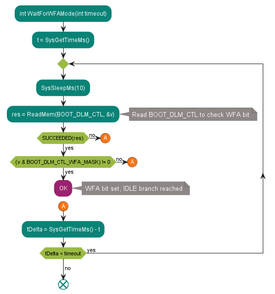
This is a helper function used in the AcquireInWFAMode subroutine. It polls the BOOT_DLM_CTL register waiting for the Boot ROM to enter WFA mode. In WFA mode, the Boot ROM is spinning in the IDLE loop waiting for the debug certificate to be loaded by the debugger.
See the code example in WaitForWFAMode.
AcquireInWFAMode
Figure 21. Acquire the device and wait for WFA mode
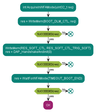
This function acquires the device in WFA mode and waits for the Boot ROM to be ready to accept the debug certificate. The debugger sets the appropriate BOOT_DLM_CTL.REQUEST and issues a software reset by setting RES_SOFT_CTL.TRIG_SOFT = 1.
See the code example in AcquireInWFAMode.
LoadDebugCert
Figure 22. Loads the debug certificate to the RAM
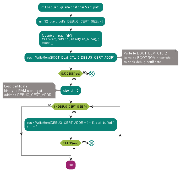
Reads the debug certificate and loads its contents to the RAM.
See the code example in LoadDebugCert.
StartWFARequest
Figure 23. Executes the WFA request
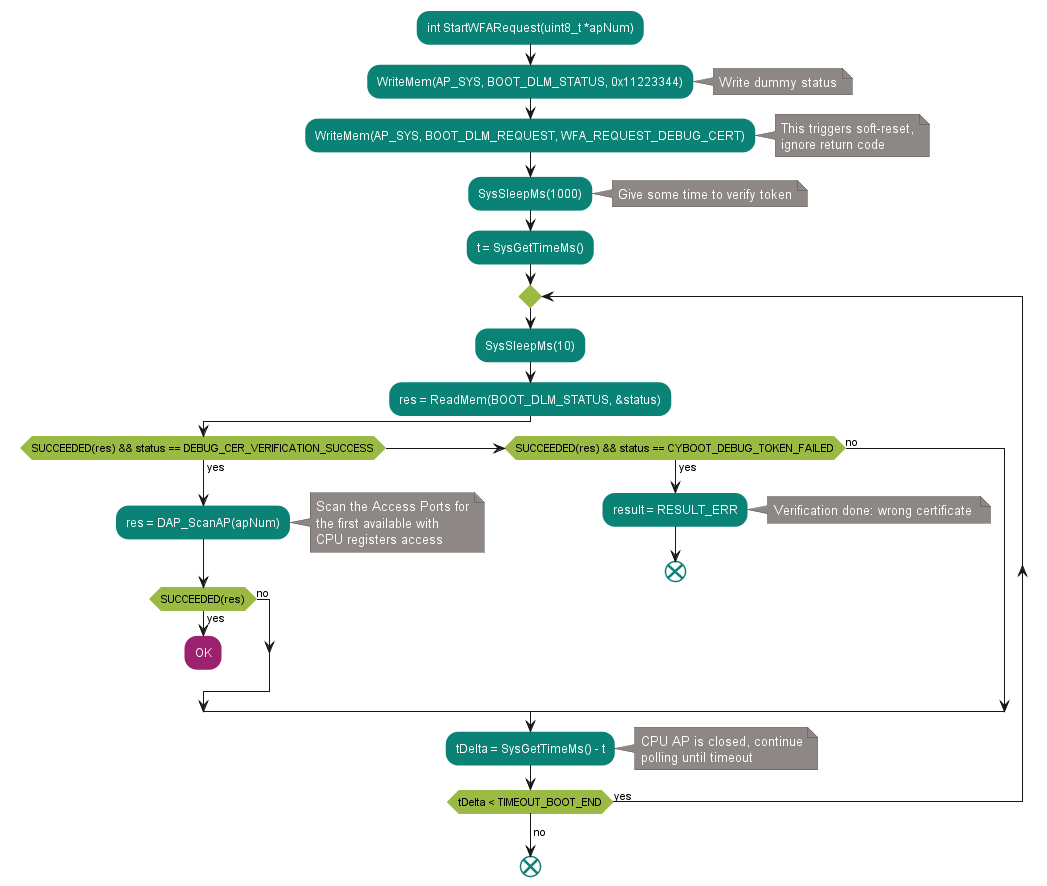
StartWFA request is executed after debug certificate is loaded at DEBUG_CERT_ADDR (and that address is also written to BOOT_DLM_CTL_2). In fact, WFA bit is now cleared to let ROM APP start reading certificate. As an indication of successful result – CM33 access point must appear in a scanning list.
See the code example in StartWFARequest.
Unlock the access to the CPU using the debug certificate
UnlockCPUAccess
Figure 24. Unlocks the access to the CM33 access port
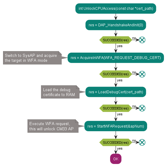
This function performs the whole unlock sequence described in
Unlock the access to the CPU (helper functions)
. After running this function, the device is reset and CM33 access port is opened by the Boot ROM. The CPU is not halted after the reset, so it starts to execute the application code. This is sufficient for the debugger to attach to the running target and observe its state.
See the code example in UnlockCPUAccess.
The application firmware is expected to follow this procedure for SWJ pin configuration:
Do not modify the configuration of the SWJ pins for parts that have a permanent SWD interface. They will be properly configured and may have already connected to the SWD probe when the firmware starts
For parts that repurpose their SWD pins:
If the SWD interface is presently active (CPUSS_DP_STATUS.SWJ_CONNECTED bit is ‘1’), leave the pins in their current state; a probe has connected during the acquire window and the pins should not be repurposed
If the SWD interface is not active, you may configure the pins and enable the alternate purpose
(use them as GPIO) such that the external debugger will not be able to communicate with the device.
Using SROM APIs to program/erase flash
As described in Acquisition algorithm, SROM API must be called after successful acquisition. SROM APIs function calling is performed by means of setting the appropriate registers of the CM33 processor as follows:
pc – program counter
sp – stack pointer
lr – linked register
r0, r1, r2 – general registers
The program counter value is filled with a pointer (see
Table 2
), depending on a desired operation. General registers hold the parameters of a SROM API. A linked register stores an address in RAM where breakpoint assembler operation code is stored. A stack pointer should contain an address of RAM, so that the function can have adequate size of memory for its operation.
Note that the data is flashed in chunks of 512 bytes. Smaller data cannot be flashed or erased. Also, functions work in blocking mode; therefore, the CPU cannot be utilized while flash operations are fulfilled.
SROM erases API usage
The pseudocode for SROM erase API utilization is shown in
Erase API usage pseudocode
. Erase SROM API erases one row of flash at a given address. The code snippet provides a method where lr holds an address of RAM when breakpoint is stored; therefore, the processor halts itself from letting know that the function is done. If the full size of flash is inserted, as shown in the code snippet
Erase API usage pseudocode
, the example application erases the entire flash.
SROM program API usage
The pseudocode for SROM program API utilization is shown in
Program API usage pseudocode
. It shows how to set core registers, where data to be written, flash context, and break pointer operation to RAM to achieve image flashing are included. Dividing the hexadecimal file into parts of 512 bytes and incrementing the start of flash bank, the entire image is programmed into flash.
Appendix A: Intel hex file format
Intel hex file records are a text representation of hexadecimal-coded binary data. Only ASCII characters are used, so the format is portable across most computer platforms. Each line (record) of Intel hex file consists of six parts, as shown in
Figure 25
.
Figure 25. Hex file record structure

Start code, one character - an ASCII colon ( : )
Byte count, two hex digits (1 byte) - specifies the number of bytes in the data field
Address, four hex digits (2 bytes) - a 16-bit address of the beginning of the memory position for the data
Record type, two hex digits (00 to 05) - defines the type of the data field. The record types used in the hex file generated by Infineon are as follows:
00 - Data record, which contains the data and 16-bit address
01 - End of file record, which is a file termination record and has no data. This must be the last line of the file; only one is allowed for every file
04 - Extended linear address record, which allows full 32-bit addressing. The address field is 0000, the byte count is 02. The two data bytes represent the upper 16 bits of the 32-bit address, when combined with the lower 16-bit address of the 00-type record
Data, a sequence of ‘n’ bytes of the data, represented by 2n hex digits
Checksum, two hex digits (1 byte), which is the least significant byte of the two's complement of the sum of the values of all fields except fields 1 and 6 (start code ‘:’ byte and two hex digits of the checksum)
Examples for the different record types used in the hex file generated for the PSOC™ Control C3 MCU are as follows:
Consider that these three records are placed in consecutive lines of the hex file (chip-level protection and end of hex file).
:020000043200C8
:041000001122334442
:00000001FF
For the sake of readability, “record type” is highlighted in red and the 32-bit address of the chip-level protection is in blue.
The first record (:0200000490600A) is an extended linear address record as indicated by the value in the record type field (04). The address field is 0000, the byte count is 02. This means that there are two data bytes in this record. These data bytes (0x9060) specify the upper 16 bits of the 32-bit address of data bytes. In this case, all the data records that follow this record are assumed to have their upper 16-bit address as 0x9060 (in other words, the base address is 0x90600000). 0A is the checksum byte for this record:
0xC8 = 0x100 – (0x02+0x00+0x00+0x04+0x32+0x00).
Summary
:020000043200C8

Address: 000016 = 010
Byte count: 0216 = 210
Record type: 0416 = Extended Linear Address
Data: 320032
Checksum: C816
The next record (:0100000002FD) is a data record, as indicated by the value in the record type field (00). The byte count is 01, meaning there is only one data byte in this record (02). The 32-bit starting address for these data bytes is at address 0x90600000. The upper 16-bit address (0x9060) is derived from the extended linear address record in the first line; the lower 16-bit address is specified in the address field of this record as 0000. FD is the checksum byte for this record.
Summary
:041000001122334442

Address: 100016 = 409610
Byte count: 0416 = 410
Record type: 0016 = Data
Data:1122334416
Checksum: 4216
The last record (:00000001FF) is the end-of-file record, as indicated by the value in the record type field (01). This is the last record of the hex file.
Appendix B: Serial wire debug (SWD) protocol
The SWD protocol is a packet-based serial transaction protocol. At the pin level, it uses a single bidirectional data connection (SWDIO) and a clock connection (SWDCK). The host programmer always drives the clock line, while either the programmer or the
PSOC™
Control C3 MCU drives the data line. A complete data transfer (one SWD packet) requires 46 clocks and consists of three phases:
Packet Request– The host programmer issues a request to the PSOC™ Control C3 MCU (silicon)
Acknowledge Response– The PSOC™ Control C3 MCU (silicon) sends an acknowledgement to the host
Data Transfer Phase– The data transfer is either from the PSOC™ Control C3 MCU to the host, following a read request (RDATA), or from the host to the PSOC™ Control C3 MCU, following a write request (WDATA). This phase is present only when a packet request phase is followed by a valid (OK) acknowledge response
Figure 26 shows the timing diagrams of the read and write SWD packets.
Figure 26. Write and read SWD packet timing diagrams
The SWD packet is transmitted in the following sequence:
The start bit initiates a transfer; it is always logical ‘1’
The APnDP bit determines whether the transfer is an AP access (indicated by ‘1’) or a DP access (indicated by ‘0’)
The next bit is RnW, which is ‘1’ for read from the MCU or ‘0’ for a write to the MCU
The ADDR bits (A[3:2]) are register select bits for the access port or debug port. See
Table 3
for register definition.
The parity bit contains the parity of APnDP, RnW, and ADDR bits. This is an even parity bit. If the number of logical 1s in these bits is odd, then the parity must be ‘1’, otherwise it is ‘0’
If the parity bit is not correct, the PSOC™ Control C3 MCU ignores the header and there is no ACK response. From the host standpoint, the programming operation should be aborted and retried by doing a device reset
The stop bit is always logic ‘0’
The park bit is always logic ‘1’ and should be driven high by the host
The ACK bits are device-to-host response. Possible values are shown in
Table 6
. Note that ACK in the current SWD transfer reflects the status of the previous transfer. ‘OK ACK’ means that the previous packet was successful. WAIT response requires a data phase, as explained in the following list. For a FAULT status, the programming operation should be aborted immediately.
For a WAIT response, if the transaction is a read, the host should ignore the data read in the data phase. The PSOC™ Control C3 MCU does not drive the line and the host must not check the parity bit as well
For a WAIT response, if the transaction is a write, the data phase is ignored by the PSOC™ Control C3 MCU. However, the host must still send the data to be written from the standpoint of implementation. The data parity bit corresponding to the data should also be sent by the host
For a WAIT response, it means that the PSOC™ Control C3 MCU is processing the previous transaction. The host can try for a maximum four continuous WAIT responses to see if an OK response is received. If it fails, then the programming operation should be aborted and retried
For a FAULT response, the programming operation should be aborted and retried by doing a device reset
ACK[2:0] | SWD |
|---|---|
OK | 001 |
WAIT | 010 |
FAULT | 100 |
NACK | 111 |
The data phase includes a parity bit (even parity)
For a read packet, if the host detects a parity error, then it must abort the programming operation and try again
For a write packet, if the PSOC™ Control C3 MCU detects a parity error in the data sent by the host, it generates a FAULT ACK response in the next packet
Turnaround (TrN) phase: There is a single-cycle turnaround phase between the packet request and the ACK phases, as well as between the ACK and data phases for write transfers as shown in
Figure 26
. According to the SWD protocol, both the host and the
PSOC™
Control C3 MCU use the TrN phase to change the drive modes on their respective SWDIO lines. During the first TrN phase after packet request, the
PSOC™
Control C3 MCU starts driving the ACK data on the SWDIO line on the rising edge of SWDCK in the TrN phase. This ensures that the host can read the ACK data on the next falling edge. Thus, the first TrN cycle lasts for only a half-cycle duration. The second TrN cycle of the SWD packet is one and one-half cycle long. Neither the host nor the
PSOC™
Control C3 MCU should drive the SWDIO line during the TrN phase, as indicated by ‘z’ in Figure 26.
The address, ACK, and read and write data are always transmitted LSB first
According to the SWD protocol, the host can generate any number of SWD clock cycles between two packets with the SWDIO LOW. You should generate several dummy clock cycles (three) between two packets or make the clock free running in IDLE mode
Note: The SWD interface can be reset by clocking 50 or more cycles with the SWDIO kept HIGH. To return to the idle state, SWDIO must be clocked LOW once.
Appendix C: Joint Test Action Group (JTAG) protocol
The PSOC™ Control C3 MCU JTAG interface complies with the IEEE 1149.1 specification and provides additional instructions. There are two TAPs in the silicon:
In IOSS for boundary scan
In CPUSS DAP (IDCODE 0x4BA06477) for device debugging and programming
The two TAPs are connected in series, where TDO of the IOSS TAP is connected to TDI of the DAP TAP. See
Figure 27
.
Figure 27. IOSS/DAP TAP connection
Each TAP consists of a 35-bit data register (called DP/AP access register). The size of the instruction register is 4 bits for the DAP TAP and 18 bits for the IOSS TAP. The important instructions to program the device through JTAG are listed in Table 7.
Bit Code [3:0] | Instruction | PSOC™ Control C3 MCU function |
|---|---|---|
1110 | IDCODE | Connects TDI and TDO to the device 32-bit JTAG ID code |
1010 | DPACC | Connects TDI and TDO to the DP/AP access register (35-bit) for access to the debug port registers |
1011 | APACC | Connects TDI and TDO to the DP/AP access register (35-bit) for access to the access port registers |
1111 | BYPASS | Bypasses the device by providing a 1-bit latch (bypass register) connected between TDI and TDO |
If an instruction that is not applicable is shifted into a TAP, the TAP goes into bypass mode. In bypass mode, the data register is only 1-bit long with the contents of 0. The bypass mode is used to isolate the
PSOC™
Control C3 MCU TAP. For example, if targeting the IOSS TAP, the DAP TAP is put in bypass mode by shifting in the BYPASS instruction into its instruction register and if targeting the DAP TAP, the IOSS TAP will be placed in bypass mode. See the examples of TAP configuration in
Figure 28
.
Figure 28. IOSS/DAP TAP configuration examples
Combines instruction registers; 22 bits total
Enables access to the APACC registers of the DAP for device debugging and programming and configures the IOSS TAP in bypass mode; 36 bits total
Enables access to the IOSS APACC registers for enabling test modes and configures the DAP TAP in bypass mode; 36 bits total
Appendix D: Code example
Hardware-specific backend functions
The following code example is written in hardware-independent way so that it relies on a few backend functions which must be implemented by the user. Implementation of these functions will be different across different debug adapters and different operating systems.
This code expects that the following functions are available during linking:
extern int IsJTAG(void);
/*********************************************************************
* Returns any non-zero value if underlying transport is JTAG (zero for SWD).
*/
extern int IsJTAG(void);
extern int SetXRES(state);
/*********************************************************************
 * Controls the logic level on XRES (nSRST) pin.
 *
 * Parameters:
 *   state - value for the XRES pin (zero -> logic low, non-zero -> logic high)
 *
 * Return value:
 *   zero     - O.K.
 *   non-zero - Error
 */
extern int SetXRES(int state);
extern int SetVoltage(voltage);
/*********************************************************************
* Controls the voltage supplied by the debug adapter to power the target MCU.
* This function is optional and should return Error if not implemented.
*
* Parameters:
*   voltage - output voltage, in millivolts
*
* Return value:
*   zero     - O.K.
*   non-zero - Error
*/
extern int SetVoltage(uint32_t voltage);
extern int SWJSequence(out_bits, num_bits);
/*********************************************************************
* Generates given bit sequence on the SWDIO/TMS pin, used for JTAG->SWD and SWD->JTAG switching.
*
* Parameters:
*   out_bits - pointer to buffer containing sequence bit data, LSB first
*   num_bits - number of bits in sequence
*
* Return value:
*   zero     - O.K.
*   non-zero - Error
*/
extern int SWJSequence(const uint8_t* out_bits, size_t num_bits);
extern int Read/WriteDAP(reg, ap_n_dp, value);
/*********************************************************************
* Reads (or Writes) data to CoreSight registers.Pay attention, PSoC Control C3 is based on ADIv6 debug interface.
*
* Parameters:
*   reg - register address
*     For Read operation this parameter should take one of the following values:
*     - DP_REG_DPIDR     0x00
*     - DP_REG_CTRL_STAT 0x04
*     - DP_REG_SELECT    0x08
*     - DP_REG_RDBUFF    0x0C
*     - AP_REG_CSW       0xD00
*     - AP_REG_TAR       0xD04
*     - AP_REG_DRW       0xD0C
*     For Write operation this parameter should take one of the following values:
*     - DP_REG_ABORT     0x00
*     - DP_REG_CTRL_STAT 0x04
*     - DP_REG_SELECT    0x08
*     - DP_REG_RDBUFF    0x0C
*     - AP_REG_CSW       0xD00
*     - AP_REG_TAR       0xD04
*     - AP_REG_DRW       0xD0C
*   ap_n_dp – ‘1’ for AP registers, ‘0’ for DP registers
*   value - value to write (or pointer to the variable where read result will be stored)
*
* Return value:
*   zero     - O.K.
*   non-zero - Error
*/
extern int ReadDAP(uint8_t reg, uint8_t ap_n_dp, uint32_t* value);
extern int WriteDAP(uint8_t reg, uint8_t ap_n_dp, uint32_t value);
extern void SysSleepMs(uint32_t msec);
/*********************************************************************
* Delays execution by the given ammount of milliseconds
*
* Parameters:
*   msec - delay time in milliseconds
*
* Return value:
*   none
*/
extern void SysSleepMs(uint32_t msec);
extern int SysGetTimeMs(void);
/*********************************************************************
* Returns the number of milliseconds that have elapsed since some fixed time point in the past.
*
* Parameters:
*   none
*
* Return value:
*   number of milliseconds
*/
extern int SysGetTimeMs(void);
Constants and static data used in code
Constants
/* --- Target acquisition methods --- */

/* Initial check whether boot code is already in IDLE or DEAD branch */
#define ACQUIRE_CHECK_IDLE   (1 << 0)
/* Test mode (TM) acquisition (recommended) */
#define ACQUIRE_TEST_MODE    (1 << 1)
/* Vector Catch */
#define ACQUIRE_VECTOR_CATCH (1 << 2)
#define ACQUIRE_METHOD_ALLOWED (ACQUIRE_TEST_MODE | ACQUIRE_VECTOR_CATCH )

/* --- MCU reset types --- */

/* Hardware reset (XRES)*/
#define RST_TYPE_XRES         (1 << 0)
/* Hardware reset (Power Cycle) */
#define RST_TYPE_POWER        (1 << 1)
/* Software reset (RES_SOFT_CTL.TRIGGER_SOFT) */
#define RST_TYPE_RES_SOFT_CTL (1 << 2)
/* Software reset (AIRCR.SYSRESETREQ) */
#define RST_TYPE_SYSRESETREQ  (1 << 3)
/* Software reset (DP->CTRL/STAT.CDBGRSTREQ) */
#define RST_TYPE_CDBGRSTREQ   (1 << 4)
#define RST_TYPE_SOFT         (RST_TYPE_RES_SOFT_CTL | RST_TYPE_SYSRESETREQ | RST_TYPE_CDBGRSTREQ)
#define RST_TYPE_HARD         (RST_TYPE_XRES | RST_TYPE_POWER)
#define RST_TYPE_ANY          (RST_TYPE_HARD | RST_TYPE_SOFT)
#define RST_TYPE_ALLOWED \
  (RST_TYPE_XRES | RST_TYPE_RES_SOFT_CTL | RST_TYPE_SYSRESETREQ | RST_TYPE_CDBGRSTREQ)

/* --- Access Ports --- */

/* AP[0] System Access Port*/
#define AP_SYS                           0
/* AP[1] Cortex-M33 Access Port */
#define AP_CM33                          1
/* Maximum number of Access Ports */
#define AP_MAX                           2
/* Prefered Access Port (AP[1] - CM33 Core is used by default in this script) */
#define AP_TO_USE                        1
/* "0" - Can use any available AP if needed; "1" - Strict AP usage to preferred only*/
#define AP_TO_USE_STRICT                 0

#define AP_CM33_ADIV6  0xF0002000     /* AP cpu num for psoc c3 in ADIv6*/
#define AP_SYS_ADIV6   0xF0000000     /* AP Sys num for psoc c3 in ADIv6*/

static const uint32_t AP_ADDR[] = { /* Array of AP adresses: */
                                 AP_SYS_ADIV6, /* Address of System Access Port - AP[0] */
                                 AP_CM33_ADIV6 /* Address of Cortex-M33 Access Port - AP[1] */
};

/* --- AP/DP registers --- */
/* DP IDCODE 0x4C013477 for SWD or 0x4BA06477 for JTAG */
#define DP_IDCODE_MSK            0xF0000FFF
#define DP_IDCODE_VAL            0x40000477

#define AP_REG_A3A2_MSK          (3u << 2u) /* Mask for Bits[3:2] of the AP register address */
#define DP_SELECT_MSK            0xFFFFFFF0 /* Mask for bits[31:4] of DP->SELECT register */
#define APV2_REG_CSW             0xD00      /* Offset of AP->CSW register (Adiv6)*/
#define APV2_REG_TAR             0xD04      /* Offset of AP->TAR register (Adiv6)*/
#define APV2_REG_DRW             0xD0C      /* Offset of AP->DRW register (Adiv6)*/
#define AP_CSW_PROT_MSK          (0x4F<<24) /* 0x4F000000:Bus access protection control mask. */
#define AP_CSW_SIZE_WORD         (2 << 0)


/* Bus access protection control for Secure access */
#define AP_CSW_PROT_VAL          (0x0B<<24)
/* Bus access protection control for Non Secure access. */
#define AP_CSW_PROT_NS_VAL       (0x4B<<24)

/* --- Target-specific registers and definitions --- */
/* Boot status result address */
#define BOOT_STATUS_ADDR            0x52200418

/* SRSS->TST_MODE: Test Mode Control Register */
#define TST_MODE               0x52200400
/* SRSS->TST_MODE.TEST_MODE (bit[31], 0x80000000):
* 1 - Indicates the chip is in test mode. 0 - Normal operation mode */
#define TST_MODE_TEST_MODE      (1 << 31)

/* RES_SOFT_CTL: Soft Reset Trigger Register */
#define RES_SOFT_CTL           0x52200410
/* RES_SOFT_CTL.TRIG_SOFT (bit[0]): Triggers a soft reset. The reset clears this bit.*/
#define RES_SOFT_CTL_TRIG_SOFT   (1 << 0)

/* -- WFA acquiring, sending debug token -- */
/* Register to ser type of request to bootROM */
/* set WFA_REQUEST_DEBUG_CERT here for WFA acquiring with debug certificate */
#define BOOT_DLM_CTL                   0x52200404
#define BOOT_DLM_CTL_WFA_MASK          0x80000000

/* Holds address of debug certificate, set DEBUG_CERT_ADDR during WFA acquiring here*/
#define BOOT_DLM_CTL_2                 0x52200408

/* BootROM sets status after WFA request*/
#define BOOT_DLM_STATUS                0x5220040C
/* Possible values for BOOT_DLM_STATUS: */
#define DEBUG_CER_VERIFICATION_SUCCESS 0x0D500084
#define CYBOOT_WFA_POLLING             0x0D500080

/* Long-style namings*/
#define SRSS_RES_SOFT_CTL           RES_SOFT_CTL
#define SRSS_RES_SOFT_CTL_TRIG_SOFT RES_SOFT_CTL_TRIG_SOFT
#define SRSS_TST_MODE               TST_MODE
#define SRSS_TST_MODE_TEST_MODE     TST_MODE_TEST_MODE


/* Mask for MODULE_ID in status word */
#define CYBOOT_ID_MSK                    0xFFF00000
/* The module IDs for BootROM in case of success */
#define CYBOOT_ID_SUCCESS                0x0D500000
/* The module IDs for BootROM in case of fail */
#define CYBOOT_ID_FAIL                   0xBAF00000
/* Mask for RESULT_CODE (status) in status word */
#define CYBOOT_STATUS_MSK                0x0000FFFF
/* Result code indicating BootROM launched the application */
#define CYBOOT_NEXT_APP_LAUNCHED         0x0D500067
/* Result code indicating BootROM reached IDLE branch */
#define CYBOOT_IDLE_BRANCH_REACHED       0x0D500068
#define BOOT_STATUS_LIS_WND         CYBOOT_IDLE_BRANCH_REACHED
#define CYBOOT_DEBUG_TOKEN_PASSED   0x0D500084 /* Debug token verified */*/
#define CYBOOT_DEBUG_TOKEN_FAILED   0x0D500085 /* Debug token verification failed */
#define CYBOOT_IMG_INVALID          0xBAF000A0 /* Image invalid/erased flash*/
#define CYBOOT_SUCCESS                        0x0D50B002
#define CYBOOT_SUCCESS_1                      0x05501000
#define CYBOOT_SUCCESS_2                      0x0800A002
#define CYBOOT_BAD_PARAM                      0xBAF00001
#define CYBOOT_LOCKED                         0xBAF00002
#define CYBOOT_STARTED                        0xBAF00003
#define CYBOOT_FINISHED                       0xBAF00004
#define CYBOOT_CANCELED                       0xBAF00005
#define CYBOOT_TIMEOUT                        0xBAF00006
#define CYBOOT_NOT_IMPLEMENTED                0xBAF00007
#define CYBOOT_FAILED                         0xBAF00008
#define CYBOOT_L1_APP_DESCR_INVALID           0xBAF00011
#define CYBOOT_SERV_APP_DESCR_INVALID         0xBAF00013
#define CYBOOT_BOOTROW_READ_FAILED            0xBAF00020
#define CYBOOT_BOOTROW_CORRUPTED              0xBAF00021
#define CYBOOT_OTP_INIT_FAILED                0xBAF00022
#define CYBOOT_OTP_READ_FAILED                0xBAF00023
#define CYBOOT_OTP_WRITE_FAILED               0xBAF00024
#define CYBOOT_OTP_SMIF_CFG_INVALID           0xBAF00025
#define CYBOOT_ASSET_FACTORY_HASH_INVALID     0xBAF00026
#define CYBOOT_PUBKEY_REQUEST_FAILED          0xBAF00030
#define CYBOOT_PUBKEY_FORMAT_INVALID          0xBAF00031
#define CYBOOT_PUBKEY_VALIDATION_FAILED       0xBAF00032
#define CYBOOT_PUBKEY_HASH_PTE_INVALID        0xBAF00033
#define CYBOOT_PUBKEY_HASH_ICV_INVALID        0xBAF00034
#define CYBOOT_PUBKEY_HASH_OEM_INVALID        0xBAF00035
#define CYBOOT_APP_VALIDATION_FAILED          0xBAF00036
#define CYBOOT_APP_LAUNCH_ADDR_INVALID        0xBAF00037
#define CYBOOT_SIGNATURE_INVALID              0xBAF00038
#define CYBOOT_MCUBOOT_INTERNAL_ASSERT        0xBAF00039
#define CYBOOT_RAM_APP_FORMAT_INVALID         0xBAF0003A
#define CYBOOT_FLASH_ADDRESS_INVALID          0xBAF00049
#define CYBOOT_FLASH_TRIM_INVALID             0xBAF0004A
#define CYBOOT_FLASH_INIT_FAILED              0xBAF0004B
#define CYBOOT_FLASH_ADDR_INVALID             0xBAF0004C
#define CYBOOT_FLASH_PARAM_INVALID            0xBAF0004D
#define CYBOOT_FAULT_UNEXPECTED               0xBAF0004E
#define CYBOOT_NUM_ZEROS_0_INVALID            0xBAF00050
#define CYBOOT_NUM_ZEROS_1_INVALID            0xBAF00051
#define CYBOOT_NUM_ZEROS_2_INVALID            0xBAF00052
#define CYBOOT_NUM_ZEROS_3_INVALID            0xBAF00053
#define CYBOOT_NUM_ZEROS_KEY_0_HASH_INVALID   0xBAF00054
#define CYBOOT_NUM_ZEROS_KEY_1_HASH_INVALID   0xBAF00055
#define CYBOOT_NUM_ZEROS_ASSET_HASH_INVALID   0xBAF00056
#define CYBOOT_NUM_ZEROS_FACTORY_HASH_INVALID 0xBAF00057
#define CYBOOT_NUM_ZEROS_SECURE_HASH_INVALID  0xBAF00058
#define CYBOOT_NUM_ZEROS_PROT_FW_HASH_INVALID 0xBAF00059
#define CYBOOT_NUM_ZEROS_FLASH_TRIMS_INVALID  0xBAF0005A

/* Note: Macro checks only for the most often DEAD codes */
#define isDEADbranch(v) v==CYBOOT_IMG_INVALID ? true:  \
                        (v==CYBOOT_APP_LAUNCH_ADDR_INVALID ? true:false)

/* Locations where function pointers on blocking flash operations are stored*/
#define SROMAPI_ERASE_ROW           0x1080FFE0
#define SROMAPI_PROGRAM_ROW         0x1080FFE4
#define SROMAPI_WRITE_ROW           0x1080FFE8

#define ROW_SIZE                    512

/* Secure sram offset */
#define SRAM_S_BASE                 0x34000000

/* Dual breakpoint code */
#define DUAL_BKPT_INSTR             0xBE00BE00

/* Redefine some arm data*/
#define R0 0
#define R1 1
#define R2 2
#define R3 3
#define SP DCRSR_REGSEL_MSP
#define LR DCRSR_REGSEL_LR
#define PC DCRSR_REGSEL_PC
#define MAX_ENTRIES 960            /* Scanning ROM tables*/

/* --- Timings --- */
#define TIMEOUT_HANDSHAKE                1000
#define TIMEOUT_BOOT_END                 1000
#define TIMEOUT_HALT_CPU                 300
#define TIMEOUT_LISTEN_WND               200

/* --- Debug Certificate --- */
#define DEBUG_CERT_SIZE             127        /* Debug token size can vary*/
#define DEBUG_CERT_ADDR             0x34004000 /* Recommended address to load debug token */
#define WFA_REQUEST_DEBUG_CERT      OEM_ROT_KEY_SIGNED

/* Token types*/
#define OEM_ROT_KEY_SIGNED          2
#define PROT_FW_ROT_KEY_SIGNED      3

/* --- Debug Access Port (DAP) --- */

/* APnDP for DP access */
#define ACC_DP                           0
/* APnDP for AP access */
#define ACC_AP                           1
/* AP->ABORT.ORUNERRCLR (bit[4], 0x00000010): Clears CTRL/STAT.STICKYORUN */
#define AP_ABORT_ORUNERRCLR              (1 << 4)
/* AP->ABORT.WDERRCLR (bit[3], 0x00000008): Clears CTRL/STAT.WDATAERR */
#define AP_ABORT_WDERRCLR                (1 << 3)
/* AP->ABORT.STKERRCLR (bit[2], 0x00000004): Clears CTRL/STAT.STICKYERR */
#define AP_ABORT_STKERRCLR               (1 << 2)
/* AP->ABORT.STKCMPCLR (bit[1], 0x00000002): Clears CTRL/STAT.STICKYERR */
#define AP_ABORT_STKCMPCLR               (1 << 1)

/* AP->SELECT.APSEL (bits[31:24], 0xFF000000): Selects an AP */
#define AP_SELECT_APSEL_RSH              24
/* DP->CTRL/STAT.CSYSPWRUPREQ (bit[30], 0x40000000): System powerup request */
#define DP_CTRL_STAT_CSYSPWRUPREQ        (1 << 30)
/* DP->CTRL/STAT.CDBGPRWUPREQ (bit[28], 0x10000000): Debug powerup request */
#define DP_CTRL_STAT_CDBGPRWUPREQ        (1 << 28)
/* DP->CTRL/STAT.CDBGRSTREQ (bit[26], 0x04000000): Debug reset request */
#define DP_CTRL_STAT_CDBGRSTREQ          (1 << 26)
/* DP->CTRL/STAT.STICKYERR ( bit[5], 0x00000020): Error in AP transaction */
#define DP_CTRL_STAT_STICKYERR           (1 << 5)
/* DP->CTRL/STAT.STICKYCMP ( bit[4], 0x00000010): Match on a pushed operations*/
#define DP_CTRL_STAT_STICKYCMP           (1 << 4)
/* DP->CTRL/STAT.STICKYORUN ( bit[1], 0x00000002): Overrun detection */
#define DP_CTRL_STAT_STICKYORUN          (1 << 1)

/* DP->CSW.Prot (bits[30:24], 0x23000000): Bus access protection control. Set to 0x23, otherwise
 * no access to CPU via core AP */
#define DP_CSW_PROT_VAL                  (0x23 << 24)
/* DP->CSW.Size ( bits[2:0], 0x00000002): Size of access <- Word (32-bits) */
#define DP_CSW_SIZE_WORD                 (2 << 0)

/* --- Flash Patch and Breakpoint Unit (FPB) --- */

/* FPB->FP_CTRL: FlashPatch Control Register in ARMv7/8-M. In ARMv6-M, it is BP_CTRL: Breakpoint
 * Control register.*/
#define FP_CTRL                          0xE0002000
/* FPB->FP_CTRL.KEY (bit[1], 0x00000002): Enables write to the register */
#define FP_CTRL_KEY                      (1 << 1)
/* FPB->FP_CTRL.ENABLE (bit[0], 0x00000001): Flash Patch global enable. Enables
 * the FPB.*/
#define FP_CTRL_ENABLE                   (1 << 0)
/* FPB->FP_COMP0: FlashPatch Comparator Register0 in ARMv7/8-M. In ARMv6-M, it is BP_COMP0:
 * Breakpoint Comparator registers0 FPB->FP_COMP.BPADDR (bits[31:1], 0xFFFFFFFE): Breakpoint
 * address. Note that the bitfields are changed vs. ARMv6/7-M */
#define FP_COMP0                         0xE0002008
/* FPB->FP_COMP.BE (bit[0], 0x00000001): Breakpoint enable */
#define FP_COMP_BE                       (1 << 0)

/* --- System Control Block (SCB) --- */

/* SCB->CPUID Base Register */
#define CPUID_ADDR                       0xE000ED00
/* SCB->AIRCR: Application Interrupt and Reset Control Register */
#define AIRCR_ADDR                       0xE000ED0C
/* SCB->AIRCR.VECTKEY (bits[31:16], 0x05FA0000): Vector Key. The value 0x05FA must be written
 * to this register */
#define AIRCR_VECTKEY_VAL                (0x05FA << 16)
/* SCB->AIRCR.SYSRESETREQ ( bit[2], 0x00000004): System Reset Request */
#define AIRCR_SYSRESETREQ                (1 << 2)

/* --- Debug Control Block (DCB) --- */

/* DCB->DHCSR: Debug Halting Control and Status Register*/
#define DHCSR_ADDR                       0xE000EDF0
/* DCB->DHCSR.DBGKEY (bits[31:16], 0xA05F0000): Must write 0xA05F to DBGKEY
 * to enable write accesses to bits[15:0] */
#define DHCSR_DBGKEY_VAL                 (0xA05F << 16)
/* DCB->DHCSR.S_SLEEP ( bit[18], 0x00040000): Indicates whether the processor is sleeping */
#define DHCSR_S_SLEEP                    (1 << 18)
/* DCB->DHCSR.S_HALT ( bit[17], 0x00020000): Indicates whether the processor is in Debug
 * state */
#define DHCSR_S_HALT                     (1 << 17)
/* DCB->DHCSR.C_HALT ( bit[1], 0x00000002): Processor halt bit */
#define DHCSR_C_HALT                     (1 << 1)
/* DCB->DHCSR.C_DEBUGEN ( bit[0], 0x00000001):
 * Halting debug enable bit (DBGKEY|C_HALT|C_DEBUGEN = 0xA05F0003)*/
#define DHCSR_C_DEBUGEN                  (1 << 0)
/* DCB->DCRSR: Debug Core Register Selector Register */
#define DCRSR_ADDR                       0xE000EDF4
/* DCB->DCRSR.REGWnR ( bit[16], 0x00010000): Specifies the access type for the transfer
 * ('0' - Read, '1' - Write)*/
#define DCRSR_REGWnR                     (1 << 16)
/* DCB->DCRSR.REGSEL (bits[6:0], 0x0000007F): Specifies the ARM core register, special-purpose
 * register, or Floating-point extension register*/
#define DCRSR_REGSEL_MSK                 0x0000007F
/* DCB->DCRSR.REGSEL = xPSR */
#define DCRSR_REGSEL_xPSR                0x10
/* DCB->DCRSR.REGSEL = Main stack pointer, MSP */
#define DCRSR_REGSEL_MSP                 0x11
/* DCB->DCRSR.REGSEL = PC/DebugReturnAddress */
#define DCRSR_REGSEL_PC                  0x0F
/* DCB->DCRDR: Debug Core Register Data Register */
#define DCRDR_ADDR                       0xE000EDF8
/* DCB->DEMCR: Debug Exception and Monitor Control Register */
#define DEMCR_ADDR                       0xE000EDFC
/* DCB->DEMCR.TRCENA (bit[24], 0x01000000): Global enable for all DWT and ITM features */
#define DEMCR_TRCENA                     (1 << 24)
/* xPSR.T (bit[24], 0x01000000): Thumb bit */
#define xPSR_T                           (1 << 24)
Static data
/******************************************************************************
* SWJ state switching sequences
*****************************************************************************/

/* JTAG to SWD - standard ARM command to switch SWJ-DP from JTAG to SWD operations:
* 1) Send at least 50 SWCLKTCK cycles with SWDIOTMS HIGH. This ensures that the current
*    interface is in its reset state. The JTAG interface detects only the 16-bit
*    JTAG-to-SWD sequence starting from the test-logic-reset state.
* 2) Send the 16-bit JTAG-to-SWD select sequence on SWDIOTMS: 0b0111 1001 1110 0111, most
*    significant bit (MSb) first. This can be represented as 0x79E7, transmitted MSB first or
*    0xE79E, transmitted least significant bit (LSb) first.
* 3) Send at least 50 SWCLKTCK cycles with SWDIOTMS HIGH. This ensures that if SWJ-DP was already
*    in SWD operation before sending the select sequence, the SWD interface enters line reset state.
* 4) Make sure SWD is ready for a start bit (min. 2 clocks with SWDIO == LOW)
* Note: Obsolete for ADIv6. Switching over the DORMANT state is preferable */
static const uint8_t bJTAG_to_SWD_len = 18 * 8;
static const uint8_t bJTAG_to_SWD[] = {
0xFF, 0xFF, 0xFF, 0xFF, 0xFF, 0xFF, 0xFF,
0x9E, 0xE7,
0xFF, 0xFF, 0xFF, 0xFF, 0xFF, 0xFF, 0xFF,
0x00, 0x00
};

/* SWD to JTAG - standard ARM command to switch SWJ-DP from SWD to JTAG operations
* 1) Send at least 50 SWCLKTCK cycles with SWDIOTMS HIGH. This ensures that the current
*    interface is in its reset state. The SWD interface detects the 16-bit
*    SWD-to-JTAG sequence only when it is in reset state.
* 2) Send the 16-bit SWD-to-JTAG select sequence on SWDIOTMS: 0b0011 1100 1110 0111, MSb first.
*    This can be represented as 0x3CE7, transmitted MSb first or 0xE73C, transmitted LSb first.
* 3) Send at least five SWCLKTCK cycles with SWDIOTMS HIGH. This ensures that if SWJ-DP was
*    already in JTAG operation before sending the select sequence, the JTAG TAP enters the
*    test-logic-reset state.
* 4) Make sure SWD is ready for a start bit (min. 2 clocks with SWDIO == LOW) */
static const uint8_t bSWD_to_JTAG_len = 18 * 8;
static const uint8_t bSWD_to_JTAG[] = {
0xFF, 0xFF, 0xFF, 0xFF, 0xFF, 0xFF, 0xFF,
0x3C, 0xE7,
0xFF, 0xFF, 0xFF, 0xFF, 0xFF, 0xFF, 0xFF,
0x00, 0x00
};

/* SWD to DORMANT - standard ARM command to switch SWJ-DP from SWD to dormant state:
* 1) Send at least 50 SWCLKTCK cycles with SWDIOTMS HIGH. This sequence ensures that the SWD
*    interface is in the reset state. The target only detects the SWD-to-DS sequence when it is
*    in the reset state. Note: Fifty-six cycles will be used here to align subsequent data.
* 2) Send the 16-bit SWD-to-DS select sequence on SWDIOTMS. This sequence can be represented as either:
*    - 0x3DC7 transmitted MSB first.
*    - 0xE3BC transmitted LSB first. */
static const uint8_t bSWD_to_DORMANT_len = 9 * 8;
static const uint8_t bSWD_to_DORMANT[] = {
0xFF, 0xFF, 0xFF, 0xFF, 0xFF, 0xFF, 0xFF,
0xBC, 0xE3
};

/* JTAG to DORMANT - standard ARM command to switch SWJ-DP from JTAG to dormant state:
* 1) Send at least five SWCLKTCK cycles with SWDIOTMS HIGH. This sequence places the JTAG TAP state
*    machine into the Test-Logic-Reset state, and selects the IDCODE instruction.
*    Note: Eight cycles will be used here to align subsequent data.
* 2) Send the recommended 31-bit JTAG-to-DS select sequence on SWDIOTMS.
*    This sequence can be represented as either:
*    - 0x2EEEEEE6 transmitted MSB first, that is, starting from bit 30.
*    - 0x33BBBBBA transmitted LSB first. */
static const uint8_t bJTAG_to_DORMANT_len = 5 * 8;
static const uint8_t bJTAG_to_DORMANT[] = {
0xFF,
0xBA, 0xBB, 0xBB, 0x33
};

/* DORMANT to SWD - standard ARM command to switch SWJ-DP from dormant state to SWD:
* 1) Send at least eight SWCLKTCK cycles with SWDIOTMS HIGH. This sequence ensures that the target is
*    not in the middle of detecting a Selection Alert sequence. The target is permitted to detect the
*    Selection Alert sequence even if this 8-cycle sequence is not present.
* 2) Send the 128-bit Selection Alert sequence on SWDIOTMS. This sequence can be represented as either:
*    - 0x49CF9046 A9B4A161 97F5BBC7 45703D98 transmitted MSB first.
*    - 0x19BC0EA2 E3DDAFE9 86852D95 6209F392 transmitted LSB first.
* 3) Send four SWCLKTCK cycles with SWDIOTMS LOW.
* 4) Send 16-bit Arm CoreSight SW-DP activation code sequence on SWDIOTMS.
*    This sequence can be represented as either:
*    - 0x58 transmitted MSB first.
*    - 0x1A transmitted LSB first.
* 5) Send a sequence to place the target into a known state - at least 50 SWCLKTCK cycles with SWDIOTMS HIGH.
*    This sequence ensures that the SWD interface is in the line reset state.
* 6) Send at least 2 idle with SWDIOTMS LOW */
static const uint8_t bDORMANT_to_SWD_len = 25 * 8;
static const uint8_t bDORMANT_to_SWD[] = {
0xFF,
0x92, 0xF3, 0x09, 0x62,
0x95, 0x2D, 0x85, 0x86,
0xE9, 0xAF, 0xDD, 0xE3,
0xA2, 0x0E, 0xBC, 0x19,
0xA0, 0xF1,
0xFF, 0xFF, 0xFF, 0xFF, 0xFF,
0x3F
};

/* DORMANT to JTAG - standard ARM command to switch SWJ-DP from dormant state to JTAG:
* 1) Send at least eight SWCLKTCK cycles with SWDIOTMS HIGH. This sequence ensures that the target is
*    not in the middle of detecting a Selection Alert sequence. The target is permitted to detect the
*    Selection Alert sequence even if this 8-cycle sequence is not present.
* 2) Send the 128-bit Selection Alert sequence on SWDIOTMS.
*    This sequence can be represented as either:
*    - 0x49CF9046 A9B4A161 97F5BBC7 45703D98 transmitted MSB first.
*    - 0x19BC0EA2 E3DDAFE9 86852D95 6209F392 transmitted LSB first.
* 3) Send four SWCLKTCK cycles with SWDIOTMS LOW.
* 4) Send 16-bit Arm CoreSight SW-DP activation code sequence on SWDIOTMS.
*    This sequence can be represented as either
*    - 0x50 transmitted MSB first.
*    - 0x0A transmitted LSB first.
* 5) Send a sequence to place the target into a known state: four SWCLKTCK cycles with SWDIOTMS LOW
*    to ensure that the TAP state machine is in the Run-Test/Idle state. Then at least five SWCLKTCK
*    cycles with SWDIOTMS HIGH to ensure that the TAP state machine is in the Test-Logic/Reset state */
static const uint8_t bDORMANT_to_JTAG_len = 20 * 8;
static const uint8_t bDORMANT_to_JTAG[] = {
0xFF,
0x92, 0xF3, 0x09, 0x62,
0x95, 0x2D, 0x85, 0x86,
0xE9, 0xAF, 0xDD, 0xE3,
0xA2, 0x0E, 0xBC, 0x19,
0xA0, 0x00,
0xFF
};
Error checking functions
SUCCEEDED
/*********************************************************************
*  Checks functions return codes:
*   ≥ 0 O.K.
*   < 0 Error
*   = -2 Not supported by the current CPU + target interface combination
*
*  Return value
*    1  SUCCEEDED
*    0  FAILED
*/
int SUCCEEDED(int result) {
if (result >= 0) {
return 1;
} else {
return 0;
}
}
FAILED
/*********************************************************************
*  Checks functions return codes:
*   ≥ 0 O.K.
*   < 0 Error
*   = -2 Not supported by the current CPU + target interface combination
*
*  Return value
*    0  SUCCEEDED
*    1  FAILED
*/
int FAILED(int result) {
if (result < 0) {
return 1;
} else {
return 0;
}
}
DAP initialization functions
ClearStickyErrors
/*********************************************************************
*  Clears any sticky errors which could be left from previous sessions.
*  Otherwise only power-down-up cycle helps to restore DAP.
*
*  Return value
*    >= 0  O.K.
*    <  0  Error
*/
static int ClearStickyErrors() {
LOG_ENTRY();

int result;
uint32_t abort_reg;
uint32_t abort_val;

if (IsJTAG()) {
/* Power up DAP and clear sticky errors using DP.CTRL/STAT:
* [30]:CSYSPWRUPREQ, [28]:CDBGPWRUPREQ, [5]:STICKYERR, [4]:STICKYCMP, [1]:STICKYORUN
* Note: for JTAG, sticky error bits are read-write enabled and writing ‘1’ to these bits clears
* associated sticky errors. For SWD, these bits are read-only and to clean the sticky errors,
* you should write to appropriate bits of DP.ABORT register*/
abort_reg = DP_REG_CTRL_STAT;
abort_val = DP_CTRL_STAT_CSYSPWRUPREQ | DP_CTRL_STAT_CDBGPRWUPREQ | DP_CTRL_STAT_STICKYERR |
          DP_CTRL_STAT_STICKYCMP | DP_CTRL_STAT_STICKYORUN;
} else {
abort_reg = DP_REG_ABORT;
abort_val = AP_ABORT_ORUNERRCLR | AP_ABORT_WDERRCLR | AP_ABORT_STKERRCLR | AP_ABORT_STKCMPCLR;
}

result = WriteDAP(abort_reg, ACC_DP, abort_val);

LOG_EXIT();
return result;
}
DAP_Handshake
/******************************************************************************
* Handshake: wait for debug interface becomes enabled after device reset.
* In the worst case, when the boot code performs application HASH verification,
* boot time varies and depends on CPU clock used by boot code. For PowerCycle,
* timeout depends on the design schematic and must be longer.
*
*  Return value
*    >= 0  O.K.
*    <  0  Error
*/
static int DAP_Handshake(void) {
LOG_ENTRY();
uint32_t v;
int tDelta;
int t      = SysGetTimeMs();
int result = RESULT_ERR;

do {
if (IsJTAG()) {
/* If the interface was left in SWD by a previous session,
 * try switching to JTAG once over the dormant state. */
SWJSequence(&bSWD_to_DORMANT[0], bSWD_to_DORMANT_len);
SWJSequence(&bDORMANT_to_JTAG[0], bDORMANT_to_JTAG_len);
} else {
/* Switch to SWD over the dormant state */
SWJSequence(&bJTAG_to_DORMANT[0], bJTAG_to_DORMANT_len);
SWJSequence(&bDORMANT_to_SWD[0], bDORMANT_to_SWD_len);
}
v = 0;
// TODO: Read IDCODE step is different in cat1d j-link scripts
ReadDAP(DP_REG_DPIDR, ACC_DP, &v);
/* DAP is responsive if we can read IDCODE */
if ((v & DP_IDCODE_MSK) == DP_IDCODE_VAL) {
_DP_SELECT_LAST = 0; /* Zeroing last used value of DP->SELECT */
result          = RESULT_OK;
break;
}
tDelta = SysGetTimeMs() - t;
} while (tDelta < TIMEOUT_HANDSHAKE); /* Timeout reached? */

LOG_EXIT(result);
return result;
DAP_Init
/******************************************************************************
*  Initialize the Debug Port for programing operations. Accepts Access Port number as input:
*   0 – System AP; 1 – CM33 AP.
*
*  Return value
*    >= 0  O.K.
*    <  0  Error
*/
static int DAP_Init(uint8_t apNum) {
LOG_ENTRY();
int result;
uint32_t reg_addr;         /* Effective AP's reg addr */
uint32_t select_reg_value; /* DP->SELECT value for acces to AP's register with given offset */
uint32_t reg_index;        /* Bits[3:2] of the address, that are used to select a specific register in a bank.
                        * Used as RegIndex in ReadDAP/WriteDAP functions */

/* Power up DAP using DP.CTRL/STAT: [30]:CSYSPWRUPREQ, [28]:CDBGPWRUPREQ
* And clear sticky errors:
* - SWD:  Using AP.ABORT register
* - JTAG: Using DP.CTRL/STAT: [5]:STICKYERR, [4]:STICKYCMP, [1]:STICKYORUN
*   For JTAG, sticky error bits are read-write enabled and writing '1' to these bits clears associated sticky errors.
*   For SWD, these bits are read-only and to clean the sticky errors, you should write to appropriate bits of
* DP.ABORT register */
if (IsJTAG()) { /* JTAG */
// TODO: In jlink script, DP-CTRL/STAT register is named DP_CTRL_ (no stat). Align across all code
result = WriteDAP(DP_REG_CTRL_STAT, ACC_DP,
                DP_CTRL_STAT_CSYSPWRUPREQ | DP_CTRL_STAT_CDBGPRWUPREQ | DP_CTRL_STAT_STICKYERR /* 0x50000020 */);
} else { /* SWD */
// TODO: In jlink script, ABORT register is named as DP (e.g. DP_ABORT_STKERRCLR)
result =
  WriteDAP(DP_REG_ABORT, ACC_DP,
           AP_ABORT_ORUNERRCLR | AP_ABORT_WDERRCLR | AP_ABORT_STKERRCLR | AP_ABORT_STKCMPCLR /* 0x0000001E */);
if (SUCCEEDED(result)) {
result = WriteDAP(DP_REG_CTRL_STAT, ACC_DP, DP_CTRL_STAT_CSYSPWRUPREQ | DP_CTRL_STAT_CDBGPRWUPREQ);  // 0x50000000
}
}

/* Initialize DP->SELECT and AP->CSW */
if (SUCCEEDED(result)) {
/* Get effective address of CSW register */
reg_addr         = AP_ADDR[apNum] + APV2_REG_CSW;
select_reg_value = reg_addr & DP_SELECT_MSK;
reg_index        = reg_addr & AP_REG_A3A2_MSK;

result = WriteDAP(DP_REG_SELECT, ACC_DP, select_reg_value); /* DP->SELECT <- select_reg_value */
if (SUCCEEDED(result)) {
_DP_SELECT_LAST = select_reg_value; /* Update last used value of DP->SELECT */

/* Set CSW (DbgSwEnable=0, Prot=0x0B, SPIDEN=0, Mode=0x0, TrInProg=0, DeviceEn=0, AddrInc=Auto-increment off,
 * Size=Word (32 bits)) */
/* Note: Set Prot bits in DAP CSW register, because of no access to CPU registers via M33 or M55 AP without these
 * bits */
if (_DOMAIN_SECURE != 0) {
    result = WriteDAP(reg_index, ACC_AP, AP_CSW_PROT_VAL | AP_CSW_SIZE_WORD); /* 0x0B000002 */
} else {
    result = WriteDAP(reg_index, ACC_AP, AP_CSW_PROT_NS_VAL | AP_CSW_SIZE_WORD); /* 0x4B000002 */
}
}
}

LOG_EXIT(result);
return result;
}
DAP_HandshakeAndInit
/*********************************************************************
*  Performs Handshake and Initializes the Debug Port Accepts Access Port number as input:
*  0 – System AP; 1 – CM33 AP.
*
*  Return value
*    >= 0  O.K.
*    <  0  Error
*/
static int DAP_HandshakeAndInit(uint8_t apNum) {
LOG_ENTRY();
int result;

result = DAP_Handshake();
if (SUCCEEDED(result)) {
result = DAP_Init(apNum);
if (SUCCEEDED(result)) {
}
}

LOG_EXIT();
return result;
}
Memory access and polling functions
ReadMem
/******************************************************************************
*  Reads 32-bit value from provided memory address.
*  Note APv2 means that reading is done due to ADIV6 (v1 is adiv5)
*
*  Return value
*    >= 0  O.K.
*    <  0  Error
*/
static int ReadMem(uint8_t apNum, uint32_t address, uint32_t *value) {
int result;
/* AP.TAR <- address */
result = WriteAPv2(apNum, APV2_REG_TAR, address);
if (SUCCEEDED(result)) {
/* AP.DRW -> value */
result = ReadAPv2(apNum, APV2_REG_DRW, value);
}

return result;
}
WriteMem
/******************************************************************************
*  Writes uint32_t value to provided memory address.
*  Note APv2 means that writing is done due to ADIV6 (v1 is adiv5)
*
*  Return value
*    >= 0  O.K.
*    <  0  Error
*/
static int WriteMem(uint8_t apNum, uint32_t address, uint32_t value) {
int result;
/* AP.TAR <- address */
result = WriteAPv2(apNum, APV2_REG_TAR, address);
if (SUCCEEDED(result)) {
/* AP.DRW <- value */
result = WriteAPv2(apNum, APV2_REG_DRW, value);
}

return result;
}
PollMem
/******************************************************************************
*  Polls for the expected bit-field value in given register
*
*  Return value
*    >= 0  O.K.
*    <  0  Error/Timeout
*/
static int PollMem(uint32_t regAddr, uint32_t fieldMsk, uint32_t rsh,
             uint32_t expectedValue, int timeout,
             uint32_t sleepBetweenPolling, uint32_t *regValue) {
LOG_ENTRY();
int result;
int t;
int tDelta;
tDelta = -1;

t = SysGetTimeMs();
do {
result = ReadMem(AP_TO_USE, regAddr, regValue);
BREAK_IF_FAILED(result);
if (((*regValue & fieldMsk) >> rsh) == expectedValue) {
result = RESULT_OK;
break;
}
/* Sleep between polling - let the CPU do its job and avoid too much garbage on SWD */
if ((sleepBetweenPolling > 0) && (tDelta >= 0 /* not first iteration*/)) {
SysSleepMs(sleepBetweenPolling);
}
tDelta = SysGetTimeMs() - t;
} while (tDelta < timeout);

LOG_EXIT(result);
return result;
}
CPU AP lookup
DAP_ScanAP
/******************************************************************************
*  Scans the Access Ports for the first available with CPU registers access.
*  In fact, MCU contains AP_CM33_ADIV6 and AP_SYS_ADIV6 APs
*  Return value
*    >= 0  O.K.
*    <  0  Error
*/
int DAP_ScanAP(uint8_t *apNum) {
LOG_ENTRY();

uint32_t v;
uint8_t currAP;
int result;

/* Try all possible Access Ports */
currAP = AP_SYS;
while (currAP < AP_MAX) {
if (currAP != AP_SYS) {
/* Initializes DAP and selects Access Port with provided number */
result = DAP_HandshakeAndInit(currAP);
if (SUCCEEDED(result)) {
  /* Try to read CPUID register @0xE000ED00 */
  result = ReadMem(currAP, CPUID_ADDR, &v);
  /* If the CPUID Implementer is ARM, the Access Port is correct (we have access to the ARM
   * registers) */
  if (SUCCEEDED(result) && ((v & 0xFF000000) == 0x41000000)) {
    *apNum = currAP;
    LOG_EXIT(result);
    return RESULT_OK;
  }
}
}
currAP += 1;
}

LOG_EXIT(result);
return RESULT_ERR;
}
Arm Core control and register access functions
ReadCoreReg
/******************************************************************************
*  Reads ARM core register, special-purpose register, or Floating-point extension register CPU must
* be halted for this operation
*
*  Return value
*    >= 0  O.K.
*    <  0  Error
*/
static int ReadCoreReg(uint32_t regsel, uint32_t *value) {
LOG_ENTRY();
int result;

/* DCRSR (0xE000EDF4) <- (REGWnR == read) | REGSEL */
result = WriteMem(AP_TO_USE, DCRSR_ADDR, (regsel & DCRSR_REGSEL_MSK));
if (SUCCEEDED(result)) {
/* DCRDR (0xE000EDF8) -> value */
result = ReadMem(AP_TO_USE, DCRDR_ADDR, value);
}

LOG_EXIT(result);
return result;
}
WriteCoreReg
/******************************************************************************
*  Writes ARM core register, special-purpose register, or Floating-point extension register CPU
* must be halted for this operation
*
*  Return value
*    >= 0  O.K.
*    <  0  Error
*/
static int WriteCoreReg(uint32_t regsel, uint32_t value) {
LOG_ENTRY();
int result;

/* DCRDR (0xE000EDF8) <- value */
result = WriteMem(AP_CM33, DCRDR_ADDR, value);
if (SUCCEEDED(result)) {
/* DCRSR (0xE000EDF4) <- (REGWnR == write) | REGSEL */
result = WriteMem(AP_CM33, DCRSR_ADDR, (DCRSR_REGWnR | (regsel & DCRSR_REGSEL_MSK)));
}

LOG_EXIT(result);
return result;
}
HaltCPU
/*********************************************************************
*  Enables debug and halts the CPU using the DHCSR register
*
*  Return value
*    >= 0  O.K.
*    <  0  Error
*/
static int HaltCPU(void) {
LOG_ENTRY();

int result;
uint32_t v;

/* Enable debug, and halt the CPU using the DHCSR register: 0xE000EDF0 <- 0xA05F0003 */
result = WriteMem(AP_TO_USE, DHCSR_ADDR, DHCSR_DBGKEY_VAL | DHCSR_C_HALT | DHCSR_C_DEBUGEN);

/* Check S_HALT bit [17] in DHCSR register (@0xE000EDF0) */
if (SUCCEEDED(result)) {
result = PollMem(DHCSR_ADDR, DHCSR_S_HALT, 0, DHCSR_S_HALT, TIMEOUT_HALT_CPU, 0, &v);
}

LOG_EXIT(result);
return result;
}
ResumeCPU
/*********************************************************************
*  Enables resumes the CPU using the DHCSR register
*
*  Return value
*    >= 0  O.K.
*    <  0  Error
*/
static int ResumeCPU(void) {
LOG_ENTRY();

int result;
uint32_t v;

/* Resume CPU (keeping debug enabled) using the DHCSR register 0xE000EDF0 <- 0xA05F0001 */
result = WriteDAP(AP_REG_TAR, ACC_AP, DHCSR_ADDR);
if (SUCCEEDED(result)) {
result = WriteDAP(AP_REG_DRW, ACC_AP, DHCSR_DBGKEY_VAL | DHCSR_C_DEBUGEN);
if (SUCCEEDED(result)) {
/* Check S_HALT (bit[17] in DHCSR register @0xE000EDF0) is cleared *Most* time, S_HALT bit is
 * cleared immediately and correct value is read here. This will eliminates excessive polling
 * and keeps SWD traffic clear*/
result = ReadDAP(AP_REG_DRW, ACC_AP, &v);
}

/* If S_HALT bit was not cleared immediately, poll for it */
if (SUCCEEDED(result) && ((v & DHCSR_S_HALT) != 0)) {
result = PollMem(DHCSR_ADDR, DHCSR_S_HALT, 0, 0, TIMEOUT_HALT_CPU, 0, &v);
}
}

LOG_EXIT();
return result;
}
System reset
Reset
/******************************************************************************
*  Resets the device using either of:
*    1. Hardware reset by toggling XRES pin
*    2. Software reset by setting the RES_SOFT_CTL.TRIGGER_SOFT bit
*    3. Software reset by setting the AIRCR.SYSRESETREQ bit
*    4. Software reset by setting the DP->CTRL/STAT.CDBGRSTREQ bit
*
*  Return value
*    >= 0  O.K.
*    <  0  Error
*/
static int Reset(uint8_t rstType, uint8_t apNum) {
LOG_ENTRY();

int result;
result = RESULT_ERR;

/* Attempt to reset the device with different methods
* Note1: do not check OK/WAIT/FAULT ACKs for the data write phase since the target immediately
* reboots.
* Note2: caller code needs to do Handshake and DAP Init after reset or in case of failure */

/* 1. Hardware reset by toggling XRES pin */
if ((rstType & RST_TYPE_XRES) != 0) {
SetXRES(0);     /* nRESET == LOW */
SysSleepMs(50); /* Make sure that device recognizes the reset */
SetXRES(1);     /* nRESET == HIGH */
result = RESULT_OK;
}

/* 2. Software reset by setting the RES_SOFT_CTL.TRIGGER_SOFT bit:
* This type of software reset can work via SYS-AP, so it is more preferable vs. SYSRESETREQ */
if (FAILED(result) && ((rstType & RST_TYPE_RES_SOFT_CTL) != 0)) {
/* AP.TAR <- @(SRSS->RES_SOFT_CTL) */
result = WriteDAP(AP_REG_TAR, ACC_AP, RES_SOFT_CTL);
if (FAILED(result)) {
result = DAP_HandshakeAndInit(apNum);
if (SUCCEEDED(result)) {
  result = WriteDAP(AP_REG_TAR, ACC_AP, RES_SOFT_CTL);
}
}
/* AP.DRW <- TRIGGER_SOFT bit */
if (SUCCEEDED(result)) {
WriteDAP(AP_REG_DRW, ACC_AP, RES_SOFT_CTL_TRIG_SOFT);
}
}

/* 3. Software reset by setting the AIRCR.SYSRESETREQ bit */
if (FAILED(result) && ((rstType & RST_TYPE_SYSRESETREQ) != 0) && (apNum != AP_SYS)) {
/* AP.TAR <- @(AIRCR 0xE000ED0C) */
result = WriteDAP(AP_REG_TAR, ACC_AP, AIRCR_ADDR);
if (FAILED(result)) {
result = DAP_HandshakeAndInit(apNum);
if (SUCCEEDED(result)) {
  result = WriteDAP(AP_REG_TAR, ACC_AP, AIRCR_ADDR);
}
}
/* AP.DRW <- 0x05FA0004 */
if (SUCCEEDED(result)) {
WriteDAP(AP_REG_DRW, ACC_AP, (AIRCR_VECTKEY_VAL | AIRCR_SYSRESETREQ));
}
}

/* 4. Software reset by setting the DP->CTRL/STAT.CDBGRSTREQ bit
* In worst case, if standard software reset via SYSRESETREQ failed, it may mean that the
* firmware did very bad things disabling the debug pins or AHB_AP access (anything behind the
* DAP). However, if we still can access the DAP registers, the last thing we could try is to
* reset the target via DP->CTRL/STAT.CDBGRSTREQ.*/
if (FAILED(result) && ((rstType & RST_TYPE_CDBGRSTREQ) != 0)) {
result = DAP_Handshake();
if (SUCCEEDED(result)) {
WriteDAP(DP_REG_CTRL_STAT, ACC_DP, DP_CTRL_STAT_CSYSPWRUPREQ | DP_CTRL_STAT_CDBGPRWUPREQ | DP_CTRL_STAT_CDBGRSTREQ);
}
}

LOG_EXIT(result);
return result;
}
ROM Boot status checking and polling
CheckIDLE
(void)apNum;
int result;
uint32_t v;

if (!(ACQUIRE_METHOD_ALLOWED & ACQUIRE_CHECK_IDLE)) {
return RESULT_ERR;
}

result = DAP_HandshakeAndInit(apNum);
if (FAILED(result)) {
return RESULT_ERR;
}

/* Read BOOT_STATUS_ADDR register and check boot status, if it indicating IDLE branch then now additional steps needed*/
result = ReadMem(AP_TO_USE, BOOT_STATUS_ADDR, &v);
if (SUCCEEDED(result)) {
if (v == CYBOOT_NEXT_APP_LAUNCHED) {
/* User application launched, test mode acquisition failed*/
return RESULT_ERR;
} else if (v == CYBOOT_IDLE_BRANCH_REACHED) {
/* Test mode succeded*/
 result = RESULT_OK;
} else if (isDEADbranch(v)) {
/* Dead branch, device acquired*/
result = RESULT_OK;
} else {
/* Possibly, corrupted state*/
result = RESULT_ERR;
}
}

LOG_EXIT(result);
return result;
}
Acquisition helper functions
AcquireTestMode
/******************************************************************************
*  Performs device acquisition in test mode:
*    1. Pre-reset (do hardware (XRES)  and connect to the DAP
*    2. Set TEST_MODE bit in TST_MODE SRSS register
*    3. Poll for the LISTEN WINDOW status in a BOOT_STATUS_ADDR register
*    4. Prepares target for debug
*
*  Return value
*    >= 0  O.K.
*    <  0  Error
*/
static int AcquireTestMode(uint8_t rstType, uint8_t apNum) {
LOG_ENTRY();

int result;
uint32_t v;

WriteMem(AP_SYS, BOOT_STATUS_ADDR, 0);

/* 1. Pre-reset (do hardware (XRES) and connect to the DAP
* --------------------------------------------------------------------------------
* a. Do hardware (XRES) reset. It is critical for Test Mode acquisition,
* so stop in case of failure.
* b. Handshake (wait for debug interface to become enabled after device reset), initialize the
* Debug Port, and select the appropriate Access Port (AP) */
result = Reset(rstType, apNum);
if (SUCCEEDED(result)) {
result = DAP_HandshakeAndInit(apNum);
}

/* 2. Set TEST_MODE bit in TST_MODE SRSS register
* --------------------------------------------------------------------------------*/
if (SUCCEEDED(result)) {
result = WriteMem(apNum, SRSS_TST_MODE, SRSS_TST_MODE_TEST_MODE);
/* Read RDBUFF to make sure that the last AP write actually happens as SW-DP may buffer/delay it
* until next DAP access*/
ReadDAP(DP_REG_RDBUFF, ACC_DP, &v);
}

/* 3. Poll for the IDLE status set by boot code and check PC points to address in ROM*/
if (SUCCEEDED(result)) {
result = IsTestModeLaunched(TIMEOUT_BOOT_END);
}

/* 4. Prepares target for debug
* --------------------------------------------------------------------------------
* a. Clear TEST_MODE bit in SRSS->TST_MODE.TEST_MODE register
* b. Set SP and PC values from the vector table. Needs to be done after Test mode acquisition to
* withdraw target from IDLE loop Otherwise, such commands as "go" or "step" will not work after
* acquisition */
if (SUCCEEDED(result)) {
result = WriteMem(AP_SYS, SRSS_TST_MODE, 0);
}


LOG_EXIT(result);
return result;
}

/******************************************************************************
*  Waits for the device to be in IDLE or DEAD branches
*
*  Return value
*    >= 0  O.K.
*    <  0  Error
*/
static int IsTestModeLaunched(int timeout) {
int result;
int t;
int tDelta;
uint32_t v;
tDelta = -1;

LOG_ENTRY();

t = SysGetTimeMs();
do {
/* Sleep between polling - let the target do its job and avoid too much garbage on SWD */
SysSleepMs(10);
result = ReadMem(AP_SYS, BOOT_STATUS_ADDR, &v);
if (SUCCEEDED(result)  && ((v == CYBOOT_IDLE_BRANCH_REACHED)
    || isDEADbranch(v))) {
  /* Device acquired in test mode or Dead branch,
  thats ok as device acquired in both cases*/
  result = RESULT_OK;
  break;
}

tDelta = SysGetTimeMs() - t;
result = RESULT_ERR;
} while (tDelta < timeout);

/*Check for later if some staff need to be done with vector table*/

LOG_EXIT(result);
return result;
}
AcquireVectorCatch
/******************************************************************************
*  Performs target acquisition using Vector Catch:
*   1. Pre-reset (do hardware (XRES) or one of the software reset) and connect to the DAP
*   2. Halt CPU, set DEMCR->VC_CORERESET, and issue software reset
*   3. Connect to the DAP and check CPU is halted
*
*  Return value
*    >= 0  O.K.
*    <  0  Error
*/
static int AcquireVectorCatch(uint8_t rstType, uint8_t apNum)
{
LOG_ENTRY();
int result;
int resultTmp;
uint32_t v;
uint32_t v1;

/* 1. Pre-reset and connect
* --------------------------------------------------------------------------------
* a. Pre-reset (do hardware (XRES) or one of the software reset) and connect to the DAP
*    Pre-reset is not critical for the Vector Catch acquisition,
*    so do not check for the result and do not stop if it is failed
* b. Handshake (wait for debug interface to become enabled after device reset),
*    initialize the Debug Port and select appropriate Access Port (AP) with the CPU access*/
if (apNum == AP_SYS) {
/* It is not possible to handle CPU state (e.g. breakpoints) via the System Access Port */
result = RESULT_ERR;
} else {
Reset(rstType, apNum);
result = DAP_HandshakeAndInit(apNum);
if (SUCCEEDED(result)) {
/* Update Current Domain Secure */
result = ReadAndInitSecure();
}
}

/* 2. Halt CPU, set DEMCR->VC_CORERESET and issue software reset
* --------------------------------------------------------------------------------
* a. Enable debug and halt CPU as quickly as possible right after Reset+Handshake+InitDAP
*    It is not mandatory to do this quickly, but there is a good chance to stop
*    in Listen window or at least prevent user application from doing too much "bad" stuff
* b. Set VC_CORERESET and TRCENA bits in DEMCR register
* c. Issue software reset*/
if (SUCCEEDED(result)) {
result = HaltCPU();
if (SUCCEEDED(result)) {
/* Set VC_CORERESET and TRCENA: DEMCR (0xE000EDFC) = 0x01000001 */
result = WriteMem(apNum, DEMCR_ADDR, DEMCR_TRCENA | DEMCR_VC_CORERESET);
if (SUCCEEDED(result)) {
  result = Reset(rstType, apNum);
}
}
}

/* 3. Connect to the DAP and check CPU is halted
* --------------------------------------------------------------------------------
* a. Handshake and initialize the Debug Port
* b. Verify reset indeed occurred and CPU is halted in debug mode
* c. Verify CPU is halted and in debug mode.
*    It must be verified in separate step after the reset confirmation to avoid raise conditions.
* d. Clear VC_CORERESET, but leave TRCENA bit enabled. Do it even in failed scenario */
if (SUCCEEDED(result)) {
result = DAP_HandshakeAndInit(apNum);
if (SUCCEEDED(result)) {
v      = DHCSR_S_RESET_ST;
result = PollMem(DHCSR_ADDR, v, 0, v, TIMEOUT_LISTEN_WND, 1, &v1);
if (SUCCEEDED(result)) {
  v      = DHCSR_S_HALT | DHCSR_C_DEBUGEN;
  result = PollMem(DHCSR_ADDR, v, 0, v, TIMEOUT_LISTEN_WND, 1, &v1);
}
}
resultTmp = WriteMem(AP_CM33, DEMCR_ADDR, DEMCR_TRCENA);  // DEMCR (0xE000EDFC) <- TRCENA
if (FAILED(resultTmp) && SUCCEEDED(result)) {
result = RESULT_ERR;
}
}

LOG_EXIT(result);
return result;
}
Acquisition function
Acquire
/******************************************************************************
* Performs a variety of Psoc C3 chip acquisition attempts:
* 1. Check if the device is already in IDLE or DEAD branches
* 2. Try to acquire in Test mode (TM). This is recommended and the only 100% reliable method. But
*    it will not work if debugger cannot meet timing requirements or Listen window is disabled.
* 3. Try to acquire using the vactor catch acquisition
*
* ! Note that XRES connection is strongly required for the hardware reset. Otherwise, neither of
* the above methods will work if the firmware does "bad" things such as:
*   - Repurposes the debug pins (intentionally or unintentionally)
*   - Disables/Protects access ports and the Listen window is turned off or too short
*   - Intentionally or unintentionally corrupts values in MMIO registers and the Listen window is
* turned off or too short In this case, there is no way for the debugger to establish even basic
* communication with the target
*
*  Return value
*    >= 0  O.K.
*    <  0  Error
*/
int Acquire(uint8_t *apNum) {
LOG_ENTRY();

int result;
uint32_t v;
uint32_t v1;
uint8_t acqMethods;
result     = RESULT_ERR;
acqMethods = ACQUIRE_METHOD_ALLOWED;

/* SysAP should always use Secure Access  */
if (*apNum == 0)
_DOMAIN_SECURE = 1;

if (acqMethods == 0) {
/* Just init DAP if all acquisition methods are disabled */
result = DAP_HandshakeAndInit(*apNum);
}

/* 1. Check whether the device is already in IDLE or DEAD branch, what is sufficient condition for
* programming, so Reset/Acquire is not needed.*/
if ((acqMethods & ACQUIRE_CHECK_IDLE) != 0) {
result = DAP_HandshakeAndInit(*apNum);
if (SUCCEEDED(result)) {
result = CheckIDLE(*apNum, TIMEOUT_BOOT_END);
}
}

/* 2. Try to acquire in Test mode (TM) */
if (FAILED(result) && (result != RESULT_ERR_CRITICAL) && ((acqMethods & ACQUIRE_TEST_MODE) != 0)) {
result = AcquireTestMode(RST_TYPE_HARD & RST_TYPES_ALLOWED, *apNum);
}

/* 3. Try to acquire using the Vector Catch */
if (((acqMethods & ACQUIRE_VECTOR_CATCH) != 0) && (result != RESULT_OK) ) {

/* If SYS-AP is not strictly preferred, try to find first available AP with CPU access */
if (*apNum == AP_SYS) {
if (AP_TO_USE_STRICT != 0) {
  result = RESULT_ERR;
} else {
  result = DAP_ScanAP(&v1);
  if (SUCCEEDED(result)) {
    *apNum = v1;
  }
}
}

if (SUCCEEDED(result)) {
result = AcquireVectorCatch(RST_TYPE_HARD & RST_TYPES_ALLOWED, *apNum);
if (FAILED(result)) {
  result = AcquireVectorCatch(RST_TYPE_SOFT & RST_TYPES_ALLOWED, *apNum);
}
}
}

LOG_EXIT(result);
return result;
}
Unlocking access to the CPU, helper functions
WaitForWFAMode
/******************************************************************************
* Polls the target (with given timeout) waiting for WFA mode to be entered
*
* Return value
*   >= 0  O.K.
*   <  0  Error
*/
static int WaitForWFAMode(int timeout)
{
LOG_ENTRY();

int result = RESULT_ERR;
int t;
int tDelta;
uint32_t v;

t = SysGetTimeMs();
do {
/* Sleep between polling - let the target do its job and avoid too much garbage on SWD */
SysSleepMs(10);

/* Read BOOT_DLM_CTL register and check the WFA bit is set, indicating a WFA mode */
result = ReadMem(AP_SYS, BOOT_DLM_CTL, &v);
if (SUCCEEDED(result)) {
if ((v & BOOT_DLM_CTL_WFA_MASK) != 0) {
  /* WFA branch reached */
  result = RESULT_OK;
  break;
}
}

tDelta = SysGetTimeMs() - t;
} while (tDelta < timeout);

LOG_EXIT(result);
return result;
}
AcquireInWFAMode
/******************************************************************************
* Acquires the target in WFA mode using specified request code
*
* Return value
*   >= 0  O.K.
*   <  0  Error
*/
static int AcquireInWFAMode(uint32_t req) {
LOG_ENTRY();
int result;

result = WriteMem(AP_SYS, BOOT_DLM_CTL, req);
if (SUCCEEDED(result)) {
/* This write triggers soft-reset causing transaction failure, ignore the error */
WriteMem(AP_SYS, RES_SOFT_CTL, RES_SOFT_CTL_TRIG_SOFT);

result = DAP_HandshakeAndInit(0);
if (SUCCEEDED(result)) {
result = WaitForWFAMode(TIMEOUT_BOOT_END);
}
}
LOG_EXIT(result);
return result:
}
LoadDebugCert
/******************************************************************************
* Reads the debug certificate and loads it to the RAM into DEBUG_CERT_ADDR,
* DEBUG_CERT_ADDR is written to BOOT_DLM_CTL_2
* Return value
*   >= 0  O.K.
*   <  0  Error
*/
static int LoadDebugCert(const char *cert_path) {
LOG_ENTRY();

int result       = RESULT_OK;
size_t num_reads = 0;
uint32_t cert_buffer[DEBUG_CERT_SIZE / 4];

if (cert_path == NULL)
cert_path = "debug_cert/debug_cert_oem.bin";

struct stat s;
result = stat(cert_path, &s);
if (result) {
log_write("Failed to read the Debug Certificate '%s'", cert_path);
result = RESULT_ERR_CRITICAL;
}

if (SUCCEEDED(result) && s.st_size != DEBUG_CERT_SIZE) {
log_write("Debug Certificate size mismatch");
result = RESULT_ERR_CRITICAL;
}

/* Let BootROM know the address to seek debug token there*/
result = WriteMem(AP_SYS, BOOT_DLM_CTL_2, DEBUG_CERT_ADDR);
if (FAILED(result)) {
return result;
}

if (SUCCEEDED(result)) {
FILE *f = fopen(cert_path, "rb");
if (f) {
num_reads = fread(cert_buffer, 1, sizeof(cert_buffer), f);

if (num_reads != sizeof(cert_buffer))
  result = RESULT_ERR_CRITICAL;

fclose(f);

if (SUCCEEDED(result)) {
  for (uint32_t i = 0; i < DEBUG_CERT_SIZE / 4; i++) {
    /* Write certificate to SRAM */
    result = WriteMem(AP_SYS, DEBUG_CERT_ADDR + (i * 4), cert_buffer[i]);
    if (FAILED(result)) {
      break;
    }
  }
}
}
}

LOG_EXIT(result);
return result;
}
StartWFARequest
/******************************************************************************
* Executes WFA request. Target must be acquired in WFA mode before
* calling this function.
* Function check status of debug token verification and checks if cm33 was enabled
*
* Return value
*   >= 0  O.K.
*   <  0  Error
*/
static int StartWFARequest(uint8_t *apNum) {
LOG_ENTRY();

int result;
int status;
int t;
int tDelta;

/* Write dummy status */
WriteMem(AP_SYS, BOOT_DLM_STATUS, 0x11223344);

/* This write triggers soft-reset causing transaction failure, ignore the error */
WriteMem(AP_SYS, BOOT_DLM_CTL, WFA_REQUEST_DEBUG_CERT);

/* Wait some time until check*/
SysSleepMs(1000);

/* Poll status on accepting debug cerificate via SYS-AP s*/
t = SysGetTimeMs();
do {
SysSleepMs(10);
result = ReadMem(AP_SYS, BOOT_DLM_STATUS, &status);
if (SUCCEEDED(result) && (status == DEBUG_CER_VERIFICATION_SUCCESS)) {
  /* debug certificate passed */
  /* Scan the Access Ports for the first available with CPU registers access */
  result = DAP_ScanAP(apNum);
  if (SUCCEEDED(result)) {
    /* cm33 enabled*/
    break;
  }
} else if (SUCCEEDED(result) && (status == CYBOOT_DEBUG_TOKEN_FAILED)) {
result = RESULT_ERR;
LOG_EXIT(result);
return result;
}
} while (tDelta < TIMEOUT_BOOT_END);

LOG_EXIT(result);
return result;
}
Unlocking access to the CPU
UnlockCPUAccess
/******************************************************************************
* Unlocks the access to the CPU using given debug certificate.
* CPU is left running after calling this function. The following
* steps are performed:
* 1. Target is acquired in WFA mode with request WFA_REQUEST_DEBUG_CERT
* 2. Debug certificate is loaded into RAM
* 3. WFA request WFA_REQUEST_DEBUG_CERT is executed, this will enable CM33 AP
*
*  Return value
*    >= 0  O.K.
*    <  0  Error
*/
int UnlockCPUAccess(uint8_t apNum, const char *cert_path) {
LOG_ENTRY();

int result;

result = DAP_HandshakeAndInit(0);

if (SUCCEEDED(result))
/* Sets WFA request and waits for acknowledgment from bootROM */
result = AcquireInWFAMode(WFA_REQUEST_DEBUG_CERT);

if (SUCCEEDED(result))
/* Load debug token and address of token*/
result = LoadDebugCert(cert_path);

if (SUCCEEDED(result))
/* Set request to check certificate and check return status and if cpu enabled*/
result = StartWFARequest(&apNum);

LOG_EXIT(result);
return result;
}
Flash programming
SROM APIs description
/* Main SROM APIs are the following:
cyboot_flash_write_row - performs write operation
cyboot_flash_program_row - performs program operation
cyboot_flash_erase_row - performs erase operation
> flash_context_t ctx - flash context (for blocking operation all fields must be zero),
> *ctx - points to a RAM memory where flash context located
> *address - flash address that must be erased/programmed/written
> *data - points to RAM address where data for 1 row located (to be written/programmed)
*/
uint32_t cyboot_flash_write_row(uint32_t address, uint8_t* data, flash_context_t* ctx);
uint32_t cyboot_flash_program_row(uint32_t address, uint8_t* data, flash_context_t* ctx);
uint32_t cyboot_flash_erase_row(uint32_t address, flash_context_t* ctx);

typedef void (*cyboot_flash_callback_t)(void * ctx);

typedef struct
{
uint32_t min_count;
uint32_t max_count;
uint32_t min_page_addr;
uint32_t scratch_row_idx;
} cyboot_flash_refresh_t;

typedef struct
{
/*
* [0] 0 -BLOCKING, 1-NON-BLOCKING
* [1] RWW or STALL_READ, for BLOCKING
* [2] REFRESH_CTL, determines who provides the data for Column 33.
*   0- Flash API computes the data for column 33.
*   1- column 33 is programmed as is. Up to a caller to provide the data.
* [3] A mode for Program Sector and Program Bulk operations.
*   0- ALL
*   1- Even/Odd
*/
uint32_t flags;
uint32_t hv_params_addr;
cyboot_flash_refresh_t *refresh;

/* params for non-blocking operations */
cyboot_flash_callback_t callback_pre_irq;
cyboot_flash_callback_t callback_post_irq;
cyboot_flash_callback_t callback_complete;
uint32_t callback_param;
uint32_t state; /* A state machine - EMPTY, ERASE_0, PROGRAM_0, WRITE_0,1 */
uint32_t flash_addr; /* Non-blocking WriteRow */
uint32_t data_addr;  /* Non-blocking WriteRow */
uint32_t reserved[2]; /* size to be 8 bytes aligned */
} flash_context_t;
Erase API usage pseudocode
/* Code snippet shows how to utilize ERASE SROM API
by setting CM33 core registers and proposes addresses
in RAM to be given for parameters
*/
#define ERASE_CTX_OFFSET SRAM_S_BASE
#define ERASE_BKPT_OFFSET (ERASE_CTX_OFFSET + sizeof(flash_context_t))
/**
* Function erases size bytes starting from start_address
*/
bool erase_flash(uint32_t start_address, uint32_t size)
{
uint32_t erase_func_ptr;
uint32_t bkpt_offs = ERASE_CTX_OFFSET + sizeof(flash_context_t);
uint32_t bkpt = DUAL_BKPT_INSTR;
uint32_t size_erased = 0;
flash_context_t ctx = {0};
bool ret;

/* Get erase function pointer*/
ReadMem(AP_CM33, SROMAPI_ERASE_ROW, &erase_func_ptr);

/* Write necessary data to RAM: flash context, bkpt*/
uint32_t* p = &ctx;
for (int i = 0; i < sizeof(flash_context_t); ++i) {
/* Dereference pointer and write word to RAM */
uint32_t word = *p++;
WriteMem(AP_CM33, ERASE_CTX_OFFSET, word);
}

WriteMem(AP_CM33, ERASE_BKPT_OFFSET, bkpt);

/* Write Core registers*/
WriteCoreReg(SP, SRAM_S_BASE + 0x400);
WriteCoreReg(R1, ERASE_CTX_OFFSET);
WriteCoreReg(LR, ERASE_BKPT_OFFSET | 1u);

for (int i = start_address; size_erased <= size; i += ROW_SIZE) {
WriteCoreReg(R0, i);
WriteCoreReg(PC, erase_func_ptr);
/* Blocks until returns*/
ret = run_algorithm();
if (ret) {
/*error*/
return false;
}
size_erased += ROW_SIZE;
}
/* Success*/
return true;
}
Program API usage pseudocode
/* Code snippet shows how to utilize PROGRAM SROM API
by setting CM33 core registers and proposes addresses
in RAM to be given for parameters
*/
#define PROGRAM_CTX_OFFSET SRAM_S_BASE
#define PROGRAM_BKPT_OFFSET (PROGRAM_CTX_OFFSET + sizeof(flash_context_t))
#define PROGRAM_DATA_OFFSET (PROGRAM_CTX_OFFSET + sizeof(flash_context_t) + 4)
/**
* Function programs size bytes from *buffer starting from start_address
> buffer – pointer to data to be written to flash
> size of buffer
> starting address of flash
*/
bool program_flash(uint32_t start_address, const uint8_t *buffer,uint32_t size)
{
uint32_t program_func_ptr;
uint32_t bkpt_offs = PROGRAM_CTX_OFFSET + sizeof(flash_context_t);
uint32_t bkpt = DUAL_BKPT_INSTR;
uint32_t size_programmed = 0;
uint8_t* pBuffer = buffer;
flash_context_t ctx = {0};
bool ret;

/* Get erase function pointer*/
ReadMem(AP_CM33, SROMAPI_PROGRAM_ROW, &program_func_ptr);

/* Write necessary data to RAM: flash context, bkpt, data buffer*/
uint32_t* p = &ctx;
for (int i = 0; i < sizeof(flash_context_t); ++i) {
/* Dereference pointer and write word to RAM */
uint32_t word = *p++;
WriteMem(AP_CM33, PROGRAM_CTX_OFFSET, word);
}

WriteMem(AP_CM33, PROGRAM_BKPT_OFFSET, bkpt);

/* Write first row with ROW_SIZE to RAM */
uint32_t* pData = buffer;
uint32_t data_ofs = PROGRAM_DATA_OFFSET;
for (int i = 0; i < ROW_SIZE; i += 4) {
uint32_t word = *pData++;
WriteMem(AP_CM33, data_ofs, word);
data_ofs += sizeof(uint32_t);
}
pBuffer += ROW_SIZE;

/* Write Core registers*/
WriteCoreReg(SP, SRAM_S_BASE + 0x400);
WriteCoreReg(R1, PROGRAM_CTX_OFFSET);
WriteCoreReg(R2, PROGRAM_DATA_OFFSET);
WriteCoreReg(LR, PROGRAM_BKPT_OFFSET | 1u);

for (int i = start_address; size_programmed <= size; i += ROW_SIZE) {
/* write next flash address as a destination*/
WriteCoreReg(R0, i);
WriteCoreReg(PC, program_func_ptr);
/* Blocks until returns*/
ret = run_algorithm();
if (ret) {
/*error*/
return false;
}
size_programmed += ROW_SIZE;

/* Update data in data buffer is RAM*/
pData = pBuffer;
data_ofs = PROGRAM_DATA_OFFSET;
for (int i = 0; i < ROW_SIZE; i += 4) {
uint32_t word = *pData++;
WriteMem(AP_CM33, data_ofs, word);
data_ofs += sizeof(uint32_t);
}
pBuffer += ROW_SIZE;
}

/* Success*/
return true;
}
ReadAndInitSecure
/*********************************************************************
* Reads "Debug Security Control and Status Register" (DSCSR)
* and checks "Current Domain Secure" (CDS) bit
*
* Return value
*   >= 0  O.K.
*   <  0  Error
*/
int ReadAndInitSecure(void) {
LOG_ENTRY();
int result;
uint32_t v;
_DOMAIN_SECURE = 0;

result = ReadMem(AP_TO_USE, DSCSR_ADDR, &v);
if (SUCCEEDED(result)) {
_DOMAIN_SECURE = v & DSCSR_CDS;
} else {
fprintf(stderr, "Warning, DSCSR register is unaccesible. Assumed Non-secure CDS\n");
}

if (_DOMAIN_SECURE != 0) {
fprintf(stderr, "Current domain secure state: Secure\n");
} else {
fprintf(stderr, "Current domain secure state: Non-secure\n");
}

/* Read current CSW value */
result = ReadAPv2(AP_TO_USE, APV2_REG_CSW, &v);
if (SUCCEEDED(result)) {
/* Clean PROT bits */
v &= (~AP_CSW_PROT_MSK);
/* Apply proper PROT value */
if (_DOMAIN_SECURE) {
 v |= (AP_CSW_PROT_VAL & AP_CSW_PROT_MSK);
} else {
 v |= (AP_CSW_PROT_NS_VAL & AP_CSW_PROT_MSK);
}
/* Write back to CSW */
result = WriteAPv2(AP_TO_USE, APV2_REG_CSW, v);
}
LOG_EXIT(result);
return result;
}
Reads MEM-AP register of the APv2 architecture
/*********************************************************************
 * Reads MEM-AP register of the APv2 architecture (CoreSight SoC-600)
 *
 * Return value
 *   0  SUCCEEDED
 *   1  FAILED
 */
static int ReadAPv2(uint8_t apNum, uint32_t regOffset, uint32_t *value) {
  int result;
  uint32_t reg_addr;         /* Effective AP's reg addr */
  uint32_t select_reg_value; /* DP->SELECT value for acces to AP's register with given offset */
  uint32_t reg_index;        /* Bits[3:2] of the address, that are used to select a specific register in a bank,
                              * are provided with APACC transactions */
                             /* Used as RegIndex in ReadDAP/WriteDAP functions */
  reg_addr         = AP_ADDR[apNum] + regOffset;
  select_reg_value = reg_addr & DP_SELECT_MSK;
  reg_index        = reg_addr & AP_REG_A3A2_MSK;
  /* Update DP->SELECT value if needed */
  if (select_reg_value != _DP_SELECT_LAST) {
    result = WriteDAP(DP_REG_SELECT, ACC_DP, select_reg_value);
    if (SUCCEEDED(result)) {
      _DP_SELECT_LAST = select_reg_value;
    }
  } else {
    result = RESULT_OK;
  }
  /* Read AP register value */
  if (SUCCEEDED(result)) {
    result = ReadDAP(reg_index, ACC_AP, value);
  }

  return result;
}
Writes MEM-AP register of the APv2 architecture
/*********************************************************************
* Writes MEM-AP register of the APv2 architecture (CoreSight SoC-600)
*
* Return value
*   0  SUCCEEDED
*   1  FAILED
*/
static int WriteAPv2(uint8_t apNum, uint32_t regOffset, uint32_t value) {
int result;
uint32_t reg_addr;         /* Effective AP's reg addr */
uint32_t select_reg_value; /* DP->SELECT value for acces to AP's register with given offset */
uint32_t reg_index;        /* Bits[3:2] of the address, that are used to select a specific register in a bank,
                           * are provided with APACC transactions */
                          /* Used as RegIndex in ReadDAP/WriteDAP functions */
reg_addr         = AP_ADDR[apNum] + regOffset;
select_reg_value = reg_addr & DP_SELECT_MSK;
reg_index        = reg_addr & AP_REG_A3A2_MSK;
/* Update DP->SELECT value if needed */
if (select_reg_value != _DP_SELECT_LAST) {
 result = WriteDAP(DP_REG_SELECT, ACC_DP, select_reg_value);
 if (SUCCEEDED(result)) {
   _DP_SELECT_LAST = select_reg_value;
 }
} else {
 result = RESULT_OK;
}
/* Read AP register value */
if (SUCCEEDED(result)) {
 result = WriteDAP(reg_index, ACC_AP, value);
}

return result;
}
References
JTAG
Joint Test Action Group
JTAG
SWD
Serial wire debug
SWD
SWJ-DP
Serial wire JTAG debug port
SWJ-DP
DAP
Debug access port
DAP
TAP
Test access port
TAP
eFuse
Electronic fuses
eFuse
Revision history
Document revision | Date | Description of changes |
|---|---|---|
** | 2023-12-22 | Initial release. |
*A | 2024-05-16 | Updated the address for the SROM API in the Internal flash section. Fixed a typo in the Constants and subroutines used in the acquisition flow section. Updated flow of acquiring in WFA mode in the Unlock the access to the CPU (helper functions) section. |
*B | 2024-07-25 | Added structures cyboot_flash_refresh_t and cyboot_flash_callback_t. Fixed typos in register addresses related to test mode and WFA acquisition. Added DEAD branch macro with several return codes. Updated Table 2 . Added more details to the flowcharts and updated them according to Infineon branding guidelines. Added the missing flowchart to the Step 2 – acquire in test mode section. Updated boot timings. Added security initialization (TrustZone-related feature). Added more details on pseudocode erase and program flash. |
*C | 2025-01-13 | Changed note in the PSOC™ Control C3 MCU family overview section. Added a note in the Internal flash section. |
1 XRES pin is mandatory for "Reset" PSOC™ Control C3 MCU acquisition mode, but not used for "power cycle" mode.
2 VDD pin is mandatory for "power cycle" PSOC™ Control C3 MCU acquisition mode, where the programmer powers the PSOC™ Control C3 MCU and external power is not applied. For "reset" acquisition mode, the source of power supplier does not matter, so the pin is optional.
The application firmware is expected to follow this procedure for SWJ pin configuration:
Do not modify the configuration of the SWJ pins for parts that have a permanent SWD interface. They will be properly configured and may have already connected to the SWD probe when the firmware starts
For parts that repurpose their SWD pins:
If the SWD interface is presently active (CPUSS_DP_STATUS.SWJ_CONNECTED bit is ‘1’), leave the pins in their current state; a probe has connected during the acquire window and the pins should not be repurposed
If the SWD interface is not active, you may configure the pins and enable the alternate purpose
(use them as GPIO) such that the external debugger will not be able to communicate with the device.