Functional Description
The Smart I/O implements a port-wide logic array that can be used to perform routing and logic operations to peripheral and I/O signals. The following sub sections describe the block restrictions and application critical information.
Routing Fabric
The Smart I/O routing fabric is divided into two portions, where each portion is capable of accepting half of the Chip or I/O signals. The LUTs have the following structure.
LUT 7…4 are capable of accepting signals from I/O / Chip 7…4 as inputs.
LUT 3…0 are capable of accepting signals from I/O / Chip 3…0 as inputs.
The LUTs can accept any LUT output as an input.
Each LUT output is dedicated to the corresponding output I/O and Chip terminals. For example, LUT 0 can go to either I/O 0 terminal (output type) or Chip 0 terminal (output type). The LUT output cannot be routed to an input terminal type.
Single Source LUT Input
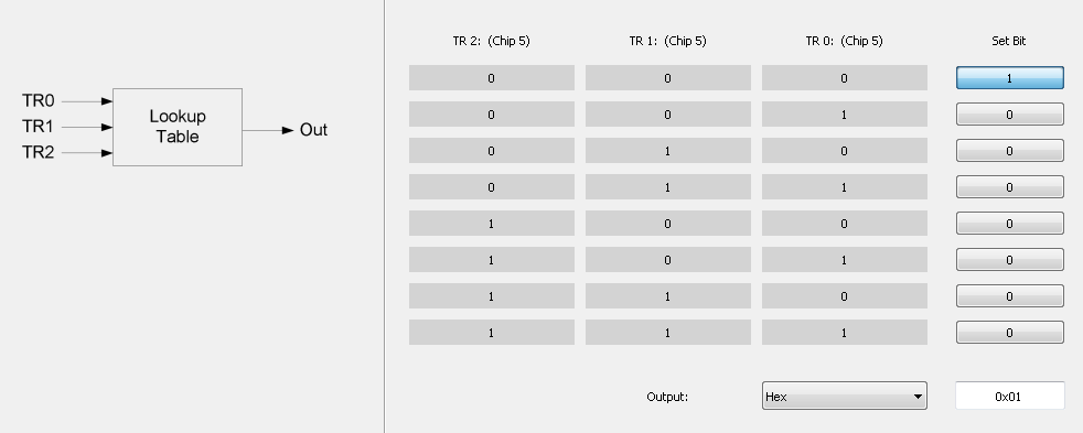
If a LUT is used, all three inputs to the LUT must be designated. For example, even If a LUT is used to accept a single source as its input, all three inputs must accept that same signal. The look-up truth table should then be designed such that it only changes the output value when all three inputs satisfy the same condition.
For example, consider the case where the signal on Chip 5 must be inverted before being passed to I/O 5. LUT 5 accepts Chip 5 as input 0, 1 and 2. The truth table is defined such that it outputs a logic 1 only when the inputs are all 0.
SCB Restriction
The SCB routing paths are restricted and can only be connected to the dedicated pin. They can however go through the dedicated LUT. For example, an SCB SPI slave select line on Chip 2 may be an input to LUT2, and then the output go to I/O 2. It cannot go to any other LUTs.
Clock and Reset behavior
The Smart I/O Configurator drives its synchronous elements using a single peripheral-wide clock. Depending on the clock source, the Configurator will have different reset behaviors, which will reset all the flip-flops in the LUTs and synchronizers to logic 0. The configuration registers will retain their values unless coming out of Power on Reset (POR).
Note:
If the Configurator is only disabled, the values in the LUT flip-flips and I/O synchronizers are held as long as the chip remains in a valid power mode.
Note:
The selected clock for the fabric’s synchronous logic is not phase aligned with other synchronous logic on the chip operating on the same clock. Therefore, communication between the Smart I/O and other synchronous logic should be treated as asynchronous (just as the communication between I/O input signals and other synchronous logic should be treated as asynchronous).
Clock source | Reset behavior | Enable delay | Description |
|---|---|---|---|
I/O 7…0 | Reset on POR | 2 clock edges | If chosen as the clock source, that particular signal cannot also be used as an input to a LUT as it may cause a race condition. The fabric will be enabled after 2 clock edges of the signal on the I/O terminal. |
Chip 7…0 | Reset on POR | 2 clock edges | If chosen as the clock source, that particular signal cannot also be used as an input to a LUT as it may cause a race condition. The fabric will be enabled after 2 clock edges of the signal on the Chip terminal. |
Peripheral Clock Divider (Active) | Reset when going to Deep Sleep, Hibernate or POR | 2 clock edges | The fabric will be enabled after 2 clock edges of the divided clock. Any synchronous logic in the LUTs will be reset to 0 when in chip deep-sleep or hibernate modes. |
Peripheral Clock Divider (Deep-Sleep) | Reset when going to Hibernate or POR | 2 clock edges | The fabric will be enabled after 2 clock edges of the divided clock. Any synchronous logic in the LUTs will be reset to 0 when in hibernate mode. |
Peripheral Clock Divider (Hibernate) | Reset on POR | 2 clock edges | The fabric will be enabled after 2 clock edges of the divided clock. |
Clk_LF | Reset when going to Hibernate and POR | 2 clock edges | The fabric will be enabled after 2 clock edges of the low frequency clock (LFCLK). Any synchronous logic in the LUTs will be reset to 0 when in hibernate mode. |
Asynchronous | Reset on POR | 3 clock edges of SYSCLK | The fabric will be enabled after 3 clock edges of the system clock (SYSCLK). |
Signal synchronization requirement
If any of the signals coming in through the Smart I/O are meant to be used in sequential elements in the LUTs, the terminal synchronizer must first be used to synchronize that signal to the peripheral clock. For example, if the signal on I/O 0 must be used in LUT0 in Sequential output mode, the synchronization for I/O 0 terminal should be enabled for reliable operation.
LUT combinatorial feedback
Since the LUTs can be configured as purely (or partially) combinatorial elements and since they can chain to each other in any fashion, combinatorial timing loops can occur. This causes oscillations that burn power and create unpredictable behavior. If a feedback is required, the signals should always go through a flip-flop before feeding back. For example, the following is a potentially problematic design. LUT1 and LUT2 are configured in
Combinatorial
mode. This will result in oscillations. To prevent it, one of the LUTs should be configured to
Gated Output
mode.
