GUI description
The top area of the QSPI Configurator is used for configuring memories; the read-only area below it displays information about the selected memory part number.
Menus
The QSPI Configurator contains the following menus.
File
New
– Creates a new Configuration file.
Open…
– Opens and loads an existing Configuration file, in either the current .
cyqspi
format or the obsolete .
cysmif
format.
Save
– Saves changes to the .
cyqspi
file. If a file has not been opened or is not in the .
cyqspi
format, the Save file dialog will open.
Save As…
– Saves changes to a new file.
Open in System Explorer
– This opens your computer’s file explorer tool to the folder that contains the Configuration file.
Import…
– Imports a specified configuration file.
Export…
– Exports the current configuration file into a specified file.
New *.cymem File…
– Creates a new memory file with default parameters. See
Create new memory file
.
Open *.cymem File…
– Opens an existing memory file.
Recent Files
– Shows up to five recent files that you can open directly.
Exit
– Closes the configurator.
Edit
Undo
– Undoes the last action or sequence of actions.
Redo
– Redoes the last undone action or sequence of undone actions.
Settings
Use Memory Folder…
– Opens a dialog to set the default path for the memory file to be saved.
ModusToolbox™ Settings
– This opens the Settings tool, an editor that allows you to configure a wide range of settings for your environment, such as proxy settings, content modes, and manifest DB settings. See the Settings tool user guide for more details on specific features.
View
Notice List
– Shows/hides the Notice List pane, which contains any errors, warnings, tasks, and information notes. See the
Device Configurator user guide
for more details.
Toolbar
– Shows/hides the Toolbar.
Reset View
– Restores the Notice List and Toolbar to the default state.
Help
Toolbar
Target Device Family
This pull-down menu shows the selected MPN for which the memory settings apply.
Flashloader Directory
A flashloader is an ELF file containing the algorithms and data structures required for flash memory programming. The QSPI Configurator can patch flashloaders so that their data structures contain data about the external flash memory that will be connected to your design, as well as how the memory is configured. The patched files are placed in the
GeneratedSource
directory alongside the source code and header files generated by the QSPI Configurator.
To enable flashloader patching, select the
Flashloader Directory
check box and use the [
…
] button to find and select the appropriate directory (or type the directory location in the text field). When you enable the
Flashloader Directory
check box, the following fields also become active to set appropriate chunk sizes:
Program Chuck Size
Erase Chunk Size
These settings allow you to control the granularity of the operations done while programming the flash memory. Larger values allow for more efficient data transfer, while smaller values can use memory more efficiently. When a memory slot is configured for Auto detect SFDP, the QSPI Configurator cannot know what values are legal, so ensure that these values are at least as large as the largest size of the program/erase operations of all the memories in use. Also, neither value can be larger than the smallest memory in use.
Note:
You can also run qspi-configurator or qspi-configurator-cli via the command line using the--flashloader-diroption. If so, the next argument must be the directory path containing the flashloader(s) to patch. If you provide this argument on the command line, the flashloader directory cannot be changed in the GUI.
Patched flashloaders
The QSPI Configurator stores files for patched flashloaders in the application directory. For Eclipse and VS Code, these files are handled automatically .
When exporting such applications to Keil µVision or IAR EWARM, these patched flashloader files must be copied into the appropriate 3
rd
party IDE directory. Refer to the
Keil µVision for ModusToolbox™ user guide
or the
IAR Embedded Workbench with ModusToolbox™ user guide
as applicable when exporting these applications.
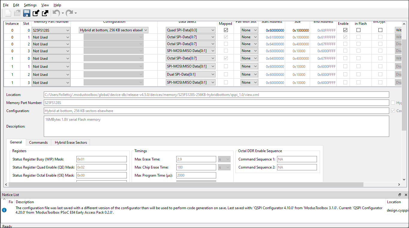
QSPI configuration fields
The top part of the QSPI Configurator contains the following parameters:
Parameter | Description |
|---|---|
QSPI Instance | This field displays when the selected device in the Target Device Family field has more than one instance. It is not editable, and it shows to which instance a given row of the table refers. |
Slave Slot | Specifies the slave slot being configured. This number corresponds to the slave select line that will be connected to the memory device. |
Memory Part Number | Device part number represents the memory device that is being interfaced to the corresponding slave slot. You can select a memory device from the list, or select the option to auto detect the device. Based on the memory device selected, the corresponding *. cymem file is linked into the slave slot. |
Configuration | For certain Memory Part Numbers , there is additional configuration information, such as 3-byte or 4-byte Addressing Mode. |
Data Select | Allows you to select the data line options for the corresponding memory slot. |
Memory Mapped | When this option is enabled, the configured memory device is mapped to the PSOC™ MCU's memory map. If disabled, access to memory must be done through the QSPI API. |
Pair with Slot | Determines the paired slot for dual Quad operation. |
Start Address | Determines the starting address where the memory device is going to be mapped in the PSOC™ memory map. |
Size | Determines size in bytes of the memory device to be mapped in the PSOC™ memory map. |
End Address | Represents the end address of the memory device as mapped in the PSOC™ MCU's memory map. This is a read-only field that is calculated automatically from "Start Address" and "Size" cells values. |
Write Enable | This lets you enable or disable writes to the external memory in a memory mapped mode of operation. |
Config Data in Flash | Determines whether a specific memory slot’s config structures are to be placed in Flash or SRAM. When chosen to be placed in SRAM, the support for the programmer is not provided. Refer to AN228740 – Usage of Quad SPI (QSPI) Serial Memory Interface (SMIF) in PSOC™ 6). |
Encrypt | Determines whether to treat the memory device in the corresponding slave slot as an encrypted device. If the memory is mapped, all access to this memory will be decrypted on-the-fly. Setting this field does expect that the right encryption key is loaded as a part of the secure image. |
Merge XIP Transactions | Specifies how many cycles can pass between memory accesses while still skipping the overhead of re-sending the read command. For CAT1A (PSOC™ 6) devices, this field must be Disabled. |
Edit memory file fields
The Edit Memory dialog contains the following fields. These fields also display as read-only in the lower part of the QSPI Configurator.
Field | Description |
|---|---|
Location | The path and file name of the current memory file. |
Memory Part Number | This is the name of the memory chip for which this configuration file is designed. This field will be displayed in the main QSPI Configurator window in the Memory Part Number drop-down menu. |
HyperBus Device | Allows you to specify HyperBus device configuration instead of the default QSPI configuration. When checked, the following tabs are hidden: General, Commands, and Hybrid Erase Sectors. When not checked, the HyperBus tab is hidden. When a HyperBus device appears in a slot, the HyperBus tab is automatically selected. Device parameters are spread between four tabs: General, Commands, Hybrid Erase Sectors, and HyperBus. |
Configuration | Some memory parts can be configured in more than one way, and each configuration is contained in a separate memory file. When creating more than one memory file for a part, use this field to describe how this file differs from the others. For example, "3-byte Addressing Mode" or "Hybrid Sectors at Bottom". |
Configuration Is Default | For memory parts with more than one configuration, this check box specifies whether this configuration is the one that should be automatically selected when this memory part is chosen in the Memory Part Number drop-down menu. |
Description | Blank field to type a description for the memory. |
General tab
Field | Description |
|---|---|
Registers | |
Status Register Busy (WIP) Mask | Mask for the busy bit in the status register. |
Status Register Quad Enable (QE) Mask | Mask for the quad enable bit in the status register. |
Status Register Octal Enable (OE) Mask | Mask for the octal enable bit in the status register. |
Octal Enable (OE) Register Address | The address to use when Read Any Register / Write Any Register commands must be used to access the octal enable register. |
Sizes | |
Size of Memory (bytes) | Denotes the actual size of the memory device. |
Program Page Size (bytes) | Denotes the page size for a program operation. This size provides the granularity with which program operations can be committed in the memory device. |
Erase Block Size (bytes) | Provides the erase block size. |
Number of Address Bytes for SPI Transactions | Sets the number of bytes that are expected for the address field in the QSPI transaction. |
Timings | |
Max Erase Time | Time the device typically takes to erase a Erase Type 1 size. You must poll the device's busy status to determine whether the operation has completed. This field has no meaning if the corresponding Erase Type size is 00h. |
Max Chip Erase Time | Typical time to erase one chip (die). You must poll the device's busy status to determine whether the operation has completed. For a device consisting of multiple dies that are individually accessed, the time is for each die to which a chip erase command is applied. |
Max Program Time (µs) | Typical time the device takes to write a full page. You must poll the device's busy status to determine whether the operation has completed. You may scale this by half or a quarter to determine approximate times for half and quarter page program operations. |
Frequency of Operations | The frequency that the memory runs at in this configuration. |
Latency Cycles | |
Mask | Mask for the latency cycles bit or bits in the status register. |
Register Address | The address to use when Read Any Register / Write Any Register commands must be used to access the latency cycles register. |
Octal DDR Enable Sequence | |
Command Sequence 1 | Specify first Octal DDR Enable Sequence. |
Command Sequence 2 | Specify second Octal DDR Enable Sequence. |
Commands tab
The
Commands
table tabs –
Single SPI
,
Dual SPI
,
Quad SPI
,
Octal SPI
– show the SPI data widths supported by the selected memory.
Field | Description |
|---|---|
Description | List of commands:
|
Number | Byte command word. |
Command Width | Width of the command transfer. |
Command Rate | Determines whether the command byte should be sent in Single Data Rate (SDR) or Double Data Rate (DDR) mode. CAT1A (PSoC™ 6) devices only support SDR. |
Address Width | Width of the address transfer. |
Address Rate | Determines whether the address bytes should be sent in SDR or DDR mode. CAT1A (PSoC™ 6) devices only support SDR. |
Mode | Provides the mode word for the command. |
Mode Width | Provides the width of the mode word transfer. |
Mode Rate | Determines whether the mode byte should be sent in SDR or DDR mode. CAT1A (PSoC™ 6) devices only support SDR. |
Dummy Cycles | Provides the number of dummy cycles in the transfer. |
Data Width | Provides the width of data bytes in the transfer. |
Data Rate | Determines whether the data bytes should be sent in SDR or DDR mode. CAT1A (PSoC™ 6) devices only support SDR. |
Hybrid Erase Sectors tab
Field | Description |
|---|---|
Hybrid Erase Sectors | This check box specifies whether sectors of different sizes are present in this configuration. The table below contains details about those sectors. If this check box is not enabled, then there are no sectors with different sizes, and none of the other fields are active. |
Row Buttons | Use these buttons to add and delete rows, as well as move rows up and down. |
Region Table | This table contains information about the various erase sector regions:
|
HyperBus Device tab
Field | Description |
|---|---|
Device Type | Specifies type of HyperBus device. Could be Flash or SRAM. |
Size of Memory (bytes) | |
Latency Clocks | Specifies value of dummy cycles for HyperBus device. |
XIP Write Command | Specifies write command for HyperBus device. Could be Wrapped or Continuous. |
XIP Read Command | Specifies read command for HyperBus device. Could be Wrapped or Continuous. |
Attention:
Support for Hyperbus RAM (such as the S70KS1282) has been added to the QSPI Configurator for TRAVEO™ T2G and XMC7000 devices. However, if a Hyperbus flash (such as the S26KL128S) is selected in one of the memory slots, flashloader patching will fail. To avoid this, either deselect Hyperbus Flash or disable flashloader patching.