AN0026 Amplitude regulation for MHz crystal oscillator
AURIX™ TC4xx
microcontrollers
About this document
Scope and purpose
This application note describes the manual configuration process for the MHz crystal oscillator amplitude regulation. Amplitude regulation feature of the MHz crystal oscillator in TC4Dx Step AA and Step AB, TC49Nx, and TC45x devices is implemented as a peak detector (see
1
, Errata
CCU_TC.013
) with a gain limitation and is not recommended to use in customer applications. This application note describes how to configure the oscillator amplitude manually to provide the more reliable operation.
Related devices
AURIX™ TC4Dx Step AA
AURIX™ TC4Dx Step AB
AURIX™ TC49xN
AURIX™ TC45x
Intended audience
This document is intended for design engineers and developers of electronic systems that are part of the AURIX™ TC4x microcontrollers and MHz crystals integration.
AURIX™ TC4x MHz oscillator amplitude regulation issues
MHz oscillator amplitude regulation concept
The better way to provide a stable oscillator amplitude is to use the automatic amplitude regulation that keeps the amplitude value with a predefined level in the whole range of ambient temperatures, power voltages, product tolerances, etc.
The special APREN bit in the OSCCON register is intended to enable the automatic amplitude regulation for the main (MHz) oscillator. But as described in the
1
(see Errata
CCU_TC.013
), this feature is implemented in AURIX™ TC4Dx, AURIX™ TC49x, and AURIX™ TC45x MCUs as a peak detector with the oscillator gain limitation and cannot be used due to the risk of having very small oscillator input amplitude that cannot provide needed protection on possible signal noises such as EMI and ESD spikes.
A manual oscillator gain configuration is recommended to provide the maximum possible value of the XTAL1 input amplitude and not to exceed the allowed crystal drive level.
MHz oscillator amplitude regulation requirements
According to the AURIX™ TC4x Datasheet
2
, the possible MHz oscillator amplitude (peak-to-peak) range is from 1.0 V up to 3.0 V on the XTAL1 pin in the external crystal mode. These amplitude values provide the stable oscillator functionality as well as the best conditions for the oscillator signal shaper and guarantees the minimum influence of the noises and possible EMC spikes. Considering that the amplitude decreases with high temperatures, these amplitude values provide sufficient margin in the whole temperature range.
On the other hand, the high amplitude values could lead to a very high crystal-drive level that can exceed the drive-level value specified in the crystal characteristics. Especially, it is critical for modern small crystal packages like the SMD 2016(2.0 mm x 1.6 mm). This package size is increasingly used in the applications due to high requirements to miniaturization and cost reduction. It needs to be taken into consideration that not exactly the voltage amplitude on one of the crystal pads is decisive for a drive level but the current amplitude that could be measured only with a special current probe.
Especially, the amplitude regulation is important for internal load capacitances usage when it could not be guaranteed the proper capacitances values set by an application and could not be used an external damping resistance to limit the maximum current amplitude.
MHz oscillator amplitude regulation simulation results
There are some simulations performed to assess the amplitude regulation possibilities of the TC4Dx devices Step AA. The simulation results for 25 MHz and 50 MHz are shown in the
Figure 1
and
Figure 2
respectively. The horizontal axis marks correspond to GAINSEL bitfield values.
As it shown in the left side of the figures, the amplitude regulation plots are not monotonic. Some changes are implemented in TC4Dx Step AB devices in the GAINSEL bitfield configuration (see
1
) to provide more linear amplitude regulation characteristics that are shown on the right sides of the
Figure 1
and
Figure 2
.
Figure 1. Amplitude regulation simulation results for 25 MHz (Impact of AppHint CCU_TC.H19)
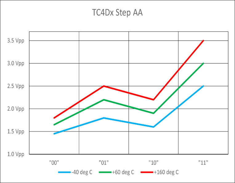 | 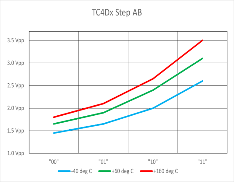 |
Figure 2. Amplitude regulation simulation results for 50 MHz (Impact of AppHint CCU_TC.H19)
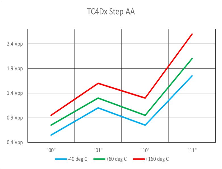 | 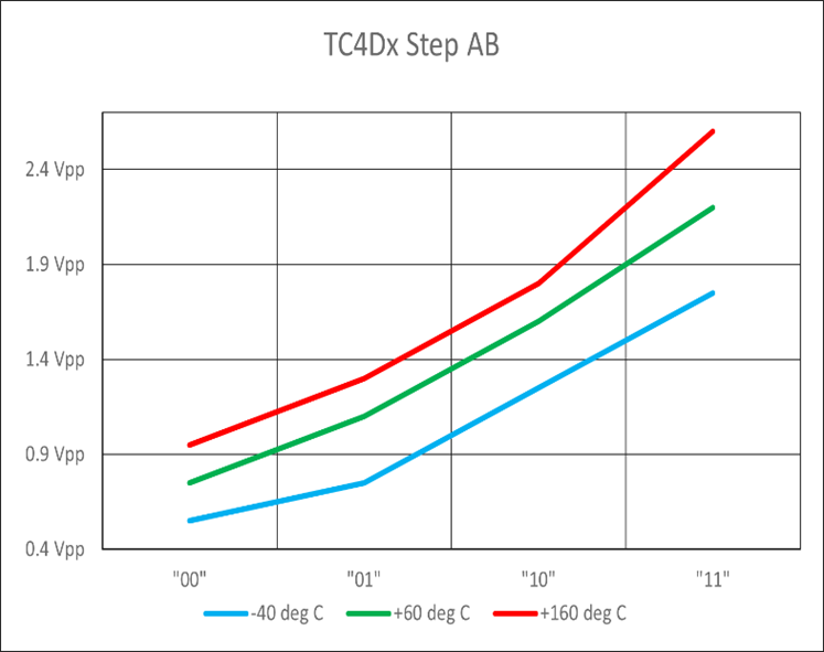 |
As it is shown in the
Figure 1
and
Figure 2
, the amplitude values more than 1.0 V are provided with the GAINSEL = 10b and 11b for 50 MHz crystals and for all GAINSEL values for 25 MHz crystals in the whole temperature range (GAINSEL values are given for the linearized step).
MHz oscillator amplitude regulation measurement results
Measurements with real crystals are performed to verify the amplitude and drive level of the AURIX™ TC4D9 devices Step AA. Increasingly used automotive industry crystal brands are chosen. Crystals are tested in SMD 3225 (3.2 mm x 2.5 mm) and in SMD 2016 (2.0 mm x 1.6 mm) packages. It is observed that the SMD 2016 became more popular due to size and cost efficiency, but they have relatively more values of an equivalent serial resistance (ESR) that leads to bigger drive level values. The measurement results for a 25 MHz 3225 and 2016 crystals are shown in the
Figure 3
and
Figure 4
respectively. The results are also shown as dependencies of drive level on amplitude in the
Figure 5
. Such a result presentation allows to assess better possible margins for both parameters. The upper curve on the left picture of
Figure 5
shows the dependency with crystal ESR increased up to 98.4 Ohm.
Figure 3. Amplitude and drive level measurement results for 25 MHz 3225 crystal
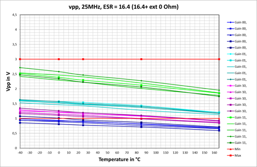 | 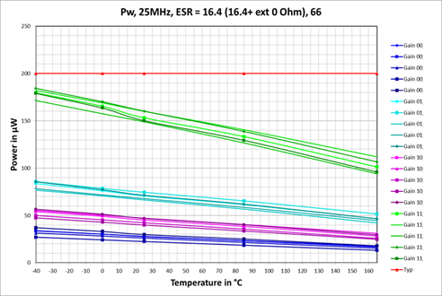 |
Figure 4. Amplitude and drive level measurement results for 25 MHz 2016 crystal
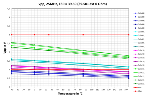 | 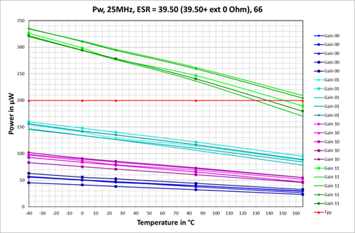 |
Figure 5. Amplitude and drive level measurement results for 25 MHz 3225 and 2016 crystals
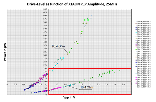 | 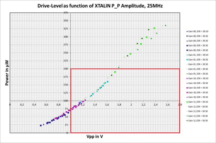 |
It is shown that the measurement results correspond to simulation ones from the
MHz oscillator amplitude regulation simulation results
. But the drive level exceeds the 300 μW value for the maximum gain configuration (GAINSEL = 11b) in case of ESR = 98.4 Ohm. In such a case, the linearized GAINSEL = 10b value should be used.
In addition to that, it should be provided at least 500 mV of an amplitude margin with a room temperature to cover the amplitude loss at high temperatures.
AURIX™ TC4x microcontrollers integration with typical MHz crystals
Recommended MHz crystals for AURIX™ TC4x microcontrollers
The more commonly used crystals for ATV MCUs have some typical technical parameters that are shown in the
Table 1
.
Parameter | 3225 Package | 2016 Package |
|---|---|---|
Nominal frequency, MHz | 16 – 54 | 16 – 60 |
Operating temperature, deg. C | -40~+150 | -40~+125(~150) |
Frequency tolerance, ppm | 10 – 100 | 10 – 100 |
Frequency temperature characteristics, ppm | ±(10 – 150) | ±(15 – 150) |
Aging, ppm | ±(3 – 5) | ±(3 – 5) |
Drive level, μW | 10 – 200 1 | 10 – 100 2 |
ESR, Ohm | 10 – 100 | 30 – 200 |
Load capacitance, pF | 8 – 12 | 8 – 12 |
As it is shown in the technical characteristics, crystals with 2016 packages have bigger ESR values that can lead to increased drive level numbers. At the same time, the 2016 crystals allow smaller drive levels that makes the process of amplitude regulation more complicated; It should be considered a tradeoff between having enough peak-to peak voltage and not to exceed drive level limitations. Usually, the high-frequency crystals (40 MHz and 50 MHz) have smaller ESR, and they are preferable to use in small 2016 packages.
AURIX™ TC4x MHz oscillator–crystal matching
As described in the user manual (see
3
), there are two approaches used for crystal–oscillator matching in AURIX™ TC4x MCUs:
External components usage like load capacitors and damping resistors
Internal components usage, so called LBoM (Low Bill of materials) mode
The first approach provides more accurate crystal-oscillator matching but it is more expensive. It allows to use damping resistors to compensate the big oscillator amplification (negative resistance) on low frequencies and to guarantee that a crystal drive level will not be exceeded.
The second approach is more cost effective but requires precise internal capacitance tuning and does not allow to use dumping resistors. In such a case, it is needed to carefully select the oscillator gain configuration and internal capacitors configuration to provide a required oscillator input amplitude and an allowed crystal drive level.
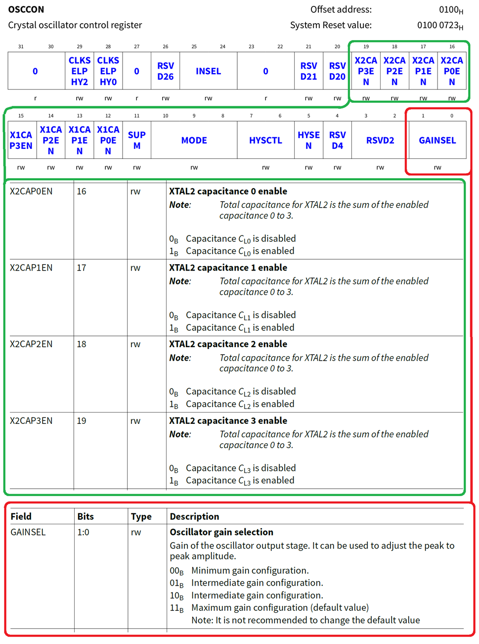
Manual AURIX™ TC4x MHz oscillator amplitude regulation configuration
Configuration parameters for amplitude regulation
The AURIX™ TC4x has only one register to configure the main (MHz) oscillator (OSCCON) that has bitfields for gain and internal capacitors configuration. The GAINSEL and X2CAPxEN bitfields are shown in the
Figure 6
. The X1CAPxEN bitfields for XTAL1 pin internal capacitance configuration are the same as X2CAPxEN just placed in the [15..12] bits. The AURIX™ TC4x main oscillator has a 3-stage amplifier and provide a big enough gain to cover the crystal frequency up to 50 MHz. This gain can be excessive at the low frequencies like 20 MHz or 25 MHz. To reduce the excessive gain, users can use the GAINSEL bitfield that is circled with a red color in the
Figure 6
. The internal capacitors should be used with LBoM mode. Users can configure a required load capacitance value by choosing the capacitor enabling bits that is circled by a green color in the
Figure 6
for XTAL2 pin. Load capacitances’ values play sufficient role in crystal matching and affect as on generated frequency tolerance as on peak-to-peak amplitude on the XTAL1 pin and crystal drive level. Thus, by tuning these bitfields customers can configure required oscillation parameters.
Figure 6. AURIX™ TC4x Main oscillator configuration register
Recommended configuration values for amplitude regulation
As mentioned, the XTAL1 pin amplitude peak-to-peak should be in a range of 1.0 V ÷ 3.0 V but at the same time, it is a requirement to have the voltage level at that pin in a range of -0.3 V ÷ 2.4 V in accordance with the datasheet
2
. Considering that the oscillator gain is decreasing with temperature, the amplitude at the room temperature should be taken with a margin at least 0.5 V (see
Figure 3
and
Figure 4
). This means that to provide minimal 1.0 V amplitude at the highest possible temperature the amplitude should be at least 1.5 V at the room temperature. The amplitude could be changed by choosing the load capacitor values and by selecting the oscillator gain (see
Figure 6
).
The capacitor values should be chosen to provide the oscillation nominal frequency but also, they could be changed to adjust the amplitude – the more capacitance values the less the amplitude value. At the same time with increasing the capacitance values the current through a crystal could be decreased that as well leads to a drive level decreasing. Also, a damping resistor could be used to decrease a drive level but only in case of external load capacitances.
After the capacitance values are defined, the oscillator gain selection should be chosen. Perform the following:
Power up the oscillator with default GAINSEL value equal to 11b (maximum gain)
Measure the amplitude on XTAL1 pin with the active probe with maximum 1 pF capacitance
If the amplitude is more than 3 V, then decrement the GAINSEL
3
value and repeat from the Step 2, else go to the next step
Measure the drive level and if it is more than specified for a crystal then decrement the GAINSEL1 value, then repeat from the Step 2
If the amplitude is less than 1.5 V in the room temperature, then decrease the capacitor values and repeat from Step 1
In any case, users should verify the final oscillator configuration with the crystal vendor and specify the capacitor values, damping resistor value (if used), amplitude at the XTAL1 pin, and drive-level dependent on temperature and assess the negative resistance as it is recommended in
3
.
Glossary
Term | Definition |
|---|---|
CCU | Clock control unit |
Drive level | The maximum possible resonator dissipative power while maintaining accuracy characteristics |
ESR | Equivalent serial resistance An equivalent electrical resistance that represents the mechanical loss in the crystal. It is used to calculate the crystal drive level |
OSC | oscillator |
References
Note: Contact Infineon support to obtain these documents.
Infineon Technologies AG:
AURIX™ TC4Dx Errata sheet
;
Available online
Infineon Technologies AG:
AURIX™ TC4Dx Datasheet
;
Available online
Infineon Technologies AG:
AURIX™ TC4Dx User manual
;
Available online
Revision history
Document revision | Date | Description of changes |
|---|---|---|
V 1.0 | 2025-02-07 | Initial release |
V1.1 | 2025-07-10 | Template update Updated the title and subtitle of the document |
1
It could be crystal produced by a special demand with the drive level up to 300 μW
2
It could be crystal produced by a special demand with the drive level up to 200 μW
3
In AURIX™ TC4Dx Step AA the GAINSEL = 01b configuration has a bigger gain than with GAINSEL = 10b