AN0019 Replacement of a failing eFlash logical sector
TriCore™
AURIX™ TC4xx family
About this document
Scope and purpose
This document explains how to replace, in the field, a failing logical sector with a free redundant one. It is applicable only for AURIX™ embedded flash (eFlash) based devices. RRAM-based devices are not covered by this document.
Intended audience
The intended audiences for this document are mainly software and firmware engineers.
Introduction
Non-volatile memories can encounter various types of faults. While the Error Correction Code (ECC) mechanism can reliably protect against bitline-oriented faults, this is not true in the case of wordline and sector-oriented faults. These failures are most likely to occur during the high voltage conditions present during writing or erase operations. Potential hard breakdowns can occur in the following areas:
Oxide between cell nodes
Oxide between contacts
Metal layer
When a hard breakdown happens, the entire content of a wordline becomes unreliable. However, the user has the possibility to repair the whole logical sector containing the failing wordline immediately using the Replace Logical Sector command. This can be done for both Program and Data flash. Due to lower voltages, the probability to have a wordline failure after a program operation is smaller than the probability of a failure after an erase operation. Although the probability to have a wordline failure is very low, it is not negligible. Therefore, a Failure Analysis Request (FAR) will be accepted only when the Replace Logical Sector command is implemented by customer applications. For more information, see the “Flash characteristics” chapter of the device-specific datasheet.
Basic principle
Failures after an erase or a program operation can also be caused by the factors beyond the hard breakdown. These may include slow cells that might need more accumulated voltage or time to be erased or programmed on the target. For this reason, in case of an Erase Verify Error (EVER flag in the error register) or Program Verify Error (PVER flag in the error register), it is always recommended to repeat the requested operation, in order to shift the few remaining cells to the target state. However, during operation, failures might also result from transient effects like voltage drops. In such cases, before repeating the operation, it is necessary to ensure a stable voltage supply (VDDEXT) and proper operating conditions.
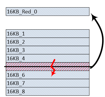
The basic functionality of the Replace Logical Sector command is to replace a failing logical sector with a free redundant one. After the successful execution of the command, the previously failing logical sector is mapped to a free redundant functional logical sector, accessible at the same address. In addition, the mapping information of the replacement is programmed into a non-volatile memory region, so that it is recovered also at the next reset (
Figure 1
). However, if an already replaced logical sector fails again, it cannot be repaired. This means that a failing redundant logical sector cannot be mapped to another redundant logical sector. In such cases, the device shall be considered as defective, and customer can apply for an FAR.
Figure 1. Replace Logical Sector principle
The tables below list the maximum number of redundant sectors available for each type of physical flash bank.
PFlash bank size | Maximum number of free redundant sectors |
|---|---|
1 MB | 3 |
2 MB | 7 |
DFlash bank size | Maximum number of free redundant sectors |
|---|---|
128 KB | 7 |
512 KB | 15 |
1 MB | 31 |
The redundant logical sectors are available for both Infineon’s production tests and customer applications. However, the number of sectors available for repair by the application may vary depending on the number of sectors used for Infineon's production tests. This number can vary for different banks. In the worst case, there might be no free redundant sectors available for the application. The number of available free redundant sectors can be retrieved by using the Count Free Redundant Sectors command. Before executing a Replace Logical Sector command, the application software needs to verify for available free redundant sectors. In the absence of free redundant sectors, the command will fail with an error (see chapter
Replace Logical Sector errors
).
The replacement feature is available for all Host and CSRM flash banks in AURIX™ TC4xx. The MCU includes two separated command interfaces: one for the Host, and one for the CSRM. Any NVM operation, including sector replacement, can be performed via a given command interface only for the banks allocated to that interface. Additionally, all the registers and flags mentioned in this document are available in both command interfaces. Always refer to the registers and flags that belong to the correct command interface. For more information, see the “bank allocation” chapter in the device-specific user manual.
Redundancy availability
AURIX™ TC4xx introduces an improvement that allows any redundant logical sector available within a specific bank to replace a failing sector in the same bank. This feature, along with the Count Free Redundant Sectors command, eliminates the need to read redundancy information from a UCB, which has been completely removed (unlike the UCB_REDSEC available in AURIX™ TC3xx).
Recommended sequence for Replace Logical Sector command
The following sequence is recommended for the execution of the Replace Logical Sector command:
Reset To Read command to reset the addressed command sequence interpreter to its initial state;
Clear Status command to clear flags;
Replace Logical Sector command;
Wait until
DMU_HCI_STATUS.REQDONE
= ‘1’;
Error flags check:
Fail if
DMU_HCI_ERR.PVER
= ‘1’;
Fail if
DMU_HCI_ERR.SQER
= ‘1’;
Fail if
DMU_HCI_ERR.PROER
= ‘1’;
Note: For information about how to handle the errors, see Chapter Replace Logical Sector errors.
Clear error flags either with the Clear Status command or by directly writing to
DMU_HCI_CLRERR
register
Note: These steps can also be done when using the CSRM command interface; in this case, use the registers DMU_CSCI_STATUS, DMU_CSCI_ERR and DMU_CSCI_CLRERR.
Critical section
The application software must always ensure that previous command sequence is not interrupted. Furthermore, the sequence shall be executed from SRAM when replacing sectors in Program Flash.
Attention: ‘Replace Logical Sector’ command shall be executed only if the device is working under normal operating conditions. Any violation of stable operating conditions during command execution can lead to severe failures (see PVER error in Chapter Replace Logical Sector errors). A reset or a power failure must also be considered as a violation of stable operating conditions. See the device-specific datasheet for a complete description of the operating conditions.
Repair after an erase operation
Based on the cell voltage conditions, it is expected that the likelihood of a wordline-oriented fail during erase operation is significantly higher than the likelihood of a hard fail during a write operation. As already described, when an EVER error is reported, it is recommended to repeat the erase operation at least once and ensure a stable voltage supply. If the EVER error persists, then a repair of the failing logical sector shall be performed. Otherwise, the write and read operations on the wordlines of the failing sector will likely fail. Furthermore, a failing erase may leave the wordlines of the concerned logical sector in an undefined (erroneous) state or an old state with an outdated data. The repair by the Replace Logical Sector command resolves these issues by providing an erased functional logical sector at the same address. Once the replacement is completed, application software can continue with the next erase operation. A possible implementation of a repair action after an erase operation is shown in
Figure 2
.
Figure 2. Repair after an erase operation
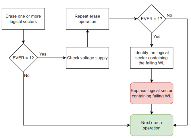
Identify failing logical sectors
The Erase Logical Sector Range command accepts two parameters: one to define the address of the first logical sector in the range, and one for the number of sectors to be erased. See the device-specific user manual for the complete description.
When an EVER error is reported for the second time (see
Figure 2
), it means that a wordline failure has occurred, and the application software must then identify the logical sector containing the failing wordline. Although the probability is very low, it is possible that multiple wordlines fail at the same time and also that the failing wordlines belong to different logical sectors. In this case, the application software must identify the number of logical sectors contain failing wordlines and their addresses. If the Erase Logical Sector Range command is targeting only one logical sector, then the identification process is straightforward. Instead, when the command is targeting multiple sectors, then the only way to identify affected sectors is to check for an EVER error for all the logical sectors in the range. The application software can either use:
Verify Erased Logical Sector Range command to verify whether a logical sector is erased
Erase Logical Sector Range command to repeat the erase operation and check for EVER flag
Note: All the logical sectors that are not reporting an EVER error are in an erased state and can be programmed normally.
To simplify the search process, a new feature is implemented in AURIX™ TC4xx. When an EVER error is reported, additional information is also available. This is described in the following table. See the device-specific user manual for a complete description.
Register | Range | Description |
|---|---|---|
COMM0 | 0 ... 255 | Number of failing logical sectors |
COMM1 | 0 ... 255 | Offset address of first failing logical sector within the sector range: 0: 1st logical sector has erase verify error 1: 2nd logical sector has erase verify error ... |
If the number of failing sectors is 1, then the offset address provided in the COMM1 register can be easily used to get the absolute address of the failing logical sector. If the number is greater than 1, then the application software can use the information provided by the COMM1 register to speed up the search process. Starting from the first failing sector, all the remaining logical sectors in the target range must be checked to find the failing ones.
Note: COMM0 and COMM1 registers are located in the FSI sub-system.
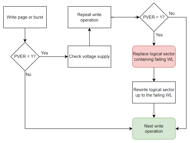
Repair after a program operation
A Wordline-oriented failures may also happen after a program operation. For this reason, replacing a failing wordline is one available option to mitigate the risk of having a fault after a program operation. Similar to repeating an erase operation, as recommended in section
Repair after an erase operation
, the application software should repeat a failing write operation at least once. This may help to shift the remaining cells (potentially a few) to the target program state.
shows a possible implementation of a repair action, particularly valid for PFlash. A typical bootloader updates entire sectors of PFlash, so there is no need to read the current content as a backup in the event of a programming error leading to a sector replacement. If the current content of a sector needs to be preserved, it is up to application software to back up the current content, execute Replace Logical Sector, and then rewrite the content. When the content of the logical sector is restored, the PFlash update process can continue.
It is important to note that wordline-oriented failures may be detected not only when a PVER occurs. . Therefore, always refer to the device-specific safety manual to find out which NVM safety mechanisms need to be considered for safety relevant applications.
Figure 3. Repair after a program operation for PFlash use case
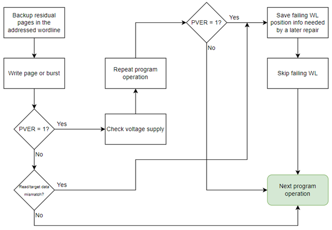
shows a possible implementation of a repair action, particularly valid for DFlash. In this case, logical sector replacement is done immediately after a hard fail detection (either PVER, or a mismatch between read and target pages in the wordline). An alternative approach (see
Figure 5
) consists of skipping the failing wordline when a hard fail is detected. The logical sector containing the failing wordline can be replaced later when the stored data is no longer needed (e.g., when the logical sector is erased). In this case, no logical sector backup is needed before replacement, but the software complexity is higher because application software must be able to save the position of the failing wordline and skip it until the repair is possible.
Robust EEPROM emulation
A wordline-oriented failure can corrupt any page(s) within the target wordline , including pages that are already written. To implement a robust EEPROM emulation, before writing a page into a wordline, it is required to save into an SRAM buffer the content of those pages (from the addressed wordline) which already contain valid data (so called residual pages). Normally a PVER flag is always set in case of a hard fail after a program operation. However, even if no PVER error is reported, it is still required to check that all the pages already written in the affected wordline match with target data. In case of a mismatch, the wordline must be considered failing.
Figure 4. Repair after a program operation for DFlash use case with immediate repair
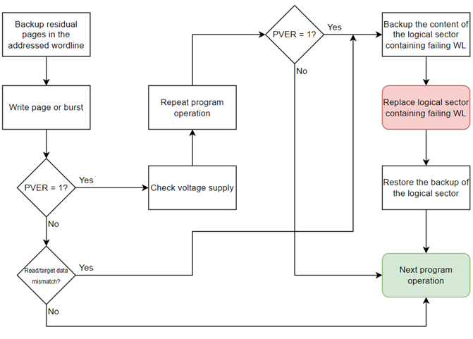
Figure 5. Repair after a program operation for DFlash use case with later repair
Replace Logical Sector errors
The Replace Logical Sector command is only successful when no errors are reported via the DMU error register. See the device-specific user manual to have a complete description of all possible errors. The following is the summary of possible errors that may occur, which includes,
Sequence Error (SQER) occurs when misaligned or wrong addresses are used
Protection Error (PROER) is triggered by incorrect configuration of various protection mechanisms.
Erase Verify Error (EVER) occurs when there is no free redundant logical sectors are available in the target bank
Program Verify Error (PVER) is a critical error that occurs when there is an error during the programming of the redundancy information. It can indicate that the redundancy information is corrupted in non-volatile memory. No repetitions of the command are possible and depending on the programming error type, the device may no longer boot.
References
Infineon Technologies AG:
AURIX™ TC4xx User Manual
Infineon Technologies AG:
AURIX™ TC4xx Datasheet
Revision history
Document revision | Date | Description of changes |
|---|---|---|
V 1.0 | 2024-07-24 | Initial release |
V 1.1 | 2025-07-10 | Template update No content update |