AURIX™ TC4xx overview
Infineon's AURIX™ TC4xx family of microcontrollers - a leader in real-time safety and security performance.
The AURIX™ platform is a family of high-performance, multi-core microcontrollers featuring multiple TriCore™ CPUs, a parallel-processing unit (PPU), program and data memories, interconnects and interconnect arbitration, an interrupt system, a DMA controller, and a comprehensive set of on-chip peripherals.
It is designed to meet the requirements of demanding embedded control system applications where price-performance balance, real-time responsiveness, computational power, data bandwidth, and power efficiency are critical design considerations. The platform integrates versatile on-chip peripheral units, including serial controllers, timer units, and analog-to-digital converters.
The AURIX™ platform offers:
Safe, secure, and real-time computing
A scalable, dependable, and robust architecture
An enhanced TriCore™ 1.8 multi-core architecture
Floating-point unit enhancements, including double-precision floating-point support
Virtualization support
Additional instructions for improved performance
A dedicated real-time control subsystem
Advanced routing engines
A proven ecosystem, including comprehensive software and tooling support
In the AURIX™ TC4xx product family, all peripheral units are connected to the TriCore™ CPUs and system through a flexible peripheral interconnect (FPI) and a shared resource interconnect (SRI). A number of input/output (I/O) lines on the AURIX™ TC4x ports are allocated to these peripheral units to facilitate communication with external systems.
The TriCore™ processor architecture integrates three advanced technologies into a single processing unit, delivering unprecedented levels of power, speed, and efficiency for embedded applications:
Reduced instruction set computing (RISC) processor architecture
Digital signal processing (DSP) operations and addressing modes
On-chip memories and peripherals
The RISC load-and-store architecture delivers high computational bandwidth at a low system cost. DSP operations and addressing modes provide the computational power needed to efficiently analyze complex real-world signals. The on-chip memory and peripherals are designed to handle even the most demanding, high-bandwidth, real-time embedded control system tasks.
The parallel processing unit (PPU) architecture integrates a 32-bit scalar RISC core with multiple vector data paths to enable single instruction multiple data (SIMD) operations on 8-bit, 16-bit, or 32-bit data types. The full vector processing unit is scalable, with AURIX™ devices offering vector widths of 512, 256, or 128 bits. This architecture delivers exceptional computational power for matrix- and vector-intensive applications, as well as for algorithms such as the Kalman filter for state-space control or neural network algorithms.
A quad-issue vector architecture that combines scalar and vector instructions within a single instruction bundle
32-bit scalar processing capabilities with double-precision floating-point support
Up to 512-bit wide single instruction multiple data (SIMD) vector processing capabilities
Support for vector floating-point processing
Floating-point math acceleration for enhanced computational efficiency
Multi-bank L1 vector memory with scatter-and-gather functionality
An integrated streaming transfer unit with direct memory access (DMA) capabilities and multiple physical channels
Functional overview
The AURIX™ TC4x family represents Infineon's third-generation (A3G) multicore microcontroller platform, designed for automotive real-time applications in powertrain, chassis systems, safety-critical functions, and advanced driver assistance systems (ADAS).
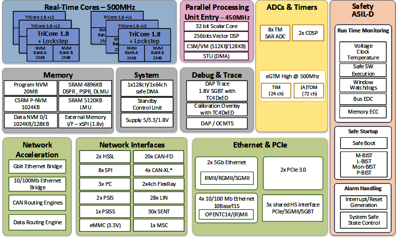
Figure 1. AURIX™ TC4D block diagram
This next-generation AURIX™ platform enhances compute performance and introduces a range of new features, building on the success of its predecessors:
Safe, real-time compute performance through the TriCore™ 1.8 multi-core architecture, operating at up to 500 MHz and fully lock-stepped for the ASIL-D safety level
CPU virtualization and system virtualization support
Up to 24 MB of on-chip non-volatile memory (NVM) with low-latency NVM access
Support for software-over-the-air (SOTA) updates with extended A/B swap functionality
Cybersecurity features and enhanced cybersecurity performance
Low-latency, high-speed communication interfaces, including 5 Gbps Ethernet and 8 Gbps PCIe, to address electrical and electronic (E/E) automotive architectures for domain control, gateway, and data fusion companion applications
Enhanced signal processing performance for powertrain and sensor data fusion applications
Low-latency, real-time signal processing for powertrain and xEV (electric vehicle) applications
Support for artificial intelligence algorithms, particularly neural network inference algorithms
Architecture enhancements to support the next generation of electrified powertrain applications
All features designed to meet the functional safety standard ISO 26262
Developed using 28 nm silicon technology to enable higher integration and lower power consumption