Top side cooled 1200V CoolSiC™ MOSFETs in Q-DPAK package for automotive applications
About this document
Scope and purpose
This application note describes the family of 1200V SiC MOSFETs in the Q-DPAK package. While intended mainly for the Onboard Charger (OBC) systems of Battery Electric Vehicles (BEV), these devices can also be used in other automotive applications like AUX inverters or eFuse. The purpose of this document is to explain the specific features of the product as well as to introduce the available material on its usage. Important application topics like gate drive and mechanical integration are covered to help design the system with maximum efficiency and power density.
Intended audience
This document is intended for circuit design engineers who develop automotive power electronics systems.
Introduction
The new generation of CoolSiC™ MOSFETs in Q-DPAK offers the performance of the 1200V Gen1p SiC technology in a Surface-mounted Top Side Cooled (TSC) high voltage package for the best system performance and power density.
The features of these new devices address the challenges of the Battery Electric Vehicle (BEV) On-Board Charger (OBC) application for which this product family is optimized.
The following is explained in the below chapters:
Specific requirements of OBC as the target application and how this new family is meeting them
Features of the new generation chip technology including fast switching and parasitic turn-on robustness
Advantages and special features of the package
Tips and recommendations such as gate driving or mechanical integration for the best thermal performance
On-Board Charger as the target application
With the fast BEV evolution and growing penetration, the charging speed at residential locations depending on the built-in OBC is a very important topic. Though OBC parameters vary and different topologies are used for both parts, some general trends can be identified which are listed below:
OBC power increasing to 11-22 kW to reduce charging time
Increasing integration and power density to 4-5 kW/l
Request for bidirectional topologies supporting V2L (Vehicle to Load) and potentially V2H (Vehicle to Home) of V2G (Vehicle to Grid) operation modes
Battery voltage increase to 800V
Typical OBC consists of a rectifier PFC stage and high-voltage to high-voltage (HVHV) as well as high-voltage to low-voltage (HVLV) DC-DC parts. Power semiconductors as critical building blocks of these parts should meet the following requirements to address the above-mentioned OBC trends:
Low conduction and switching losses for higher OBC efficiency
1200V voltage rating for the chip as well as a high voltage package with sufficient creepage distance to fit 800V Battery/system voltage
Surface-mounted TSC package for increased power density and automated assembly
Optimization of all parameters influencing system cost (including gate driver, cooling system, and passives)
Combination of high voltage and low voltage power switches on the same power PCB
The next chapters explain in more detail how the new Infineon CoolSiC™ MOSFET family helps meet these requirements.
Gen1p chip technology
Gen1p is the evolution of the first CoolSiC™ MOSFET generation Gen1 and was optimized for the OBC application profile to provide a cost-effective solution while maintaining reliability and best-in-class performance.
Gen1p CoolSiC™ chip technology advantages for OBC/DCDC
The generation “Gen1p” of Infineon’s 1200V CoolSiC™ is a significant evolution of the first 1200V generation of SiC MOSFET chip technology. With the important adjustments to the trench and gate oxide as well as the die attach technology, the Gen1p is offering an outstanding combination of key parameters and features as listed below:
Improved Rds(on) * Area to reduce chip size for the same Rds(on)
Best-in-class switching performance reducing switching losses and cooling efforts
Lowest device capacitances for higher switching speeds and higher power density
A combination of low Crss/Ciss ratio and high VGSth to avoid parasitic turn-ons (PTO) and enable unipolar gate driving
Reduced total gate charge QG for lower driving power and losses
Increased recommended turn-on voltage (VGS(on) = 20V) for lower Rds(on)
Chip metallization optimized for diffusion soldering for the best thermal performance and reliability
These chip technology features translate to the following main benefits to the application:
Improved Rds(on) resulting in lower conduction losses, higher efficiency, and reduced cooling efforts
Low switching losses allow higher switching frequencies, increase efficiency, and reduce cooling efforts
Thick Gate Oxide (GOX) contributing Rds(on) * A reduction by allowing higher VGS(on)
Low GOX Failure in Time (FIT) rate due to robust gate design/thick gate oxide
PTO robustness facilitates the system cost reduction by simplifying the gate driver
Diffusion solder-ready chip metallization improves overall thermal performance
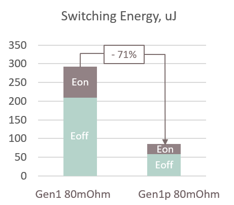
Switching performance
Switching performance is one of the key optimization factors of Gen1p chip technology. Due to reduced chip area (for the same Rds(on) ) the device capacitances were reduced significantly as can be seen in
Figure 1
for the 80 mΩ parts. Both switch-on and switch-off energy values of Gen1p 80 mΩ device reduced more than 2 times compared to Gen1. This allows for a much higher switching frequency (and thus smaller magnetic components) while keeping the same switching losses or having much lower switching losses (and less cooling effort) at the same switching frequency.
Figure 1. Improvement of Gen1p switching losses compared to the Gen1
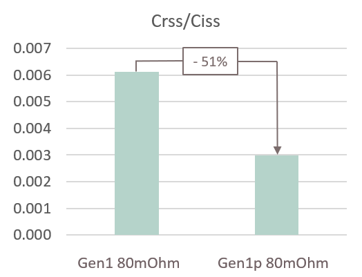
Avoiding parasitic turn-ons (PTO robustness)
It is very important to minimize or fully avoid Parasitic Turn-Ons (PTO) in the system as they may contribute substantially to the overall switching losses and thus efficiency and thermal operating point of the system. Though PCB layout and driver circuit also play a role, the PTO robustness of the MOSFET itself is key. Gen1p chips are designed PTO robust, and this is reflected in the two key parameters defining how much a MOSFET is susceptible to parasitic turn-on conditions:
C GD /C GS (also approximated as C rss /C iss ) ratio defines the level of parasitic V GS surge induced by V DS transient
V GSth (higher V GSth means lower chance for V GS surge to reach the threshold level and turn on the MOSFET)
C rss /C iss has been improved in Gen1p significantly compared to Gen1 (
Figure 2
) while V
GSth(typ)
of 4.4V is among the best in the industry.
Figure 2. The Crss/Ciss ratio of Gen1p products improved by 51% compared to Gen1
PTO-robust chip design makes the reliable zero voltage turn-off and unipolar gate driver possible (see section
Unipolar gate driving
for more details). Detailed information explaining the parasitic turn-on robustness of Gen1p technology can be found in
1
.
Package information
Benefits of the top side-cooled package in OBC/DCDC
Using surface-mounted TSC devices can significantly increase the power density of the system. The separation of electrical and thermal paths eliminates the need to use the IMS board normally used for Bottom Side-Cooled (BSC) devices to achieve low system Rth. Instead, a standard FR4 PCB can be used effectively with the driver circuit and other components placed on both sides of the PCB. From the mechanical design perspective, this can result in fewer PCBs stacked, with less volume required, as well as lower interconnect and assembly efforts (
Figure 3
). From the electrical design point of view, an important advantage is a shorter gate loop and overall lower parasitic inductances, allowing cleaner switching with lower overshoots.
Figure 3. Top Side Cooling (TSC) system advantages
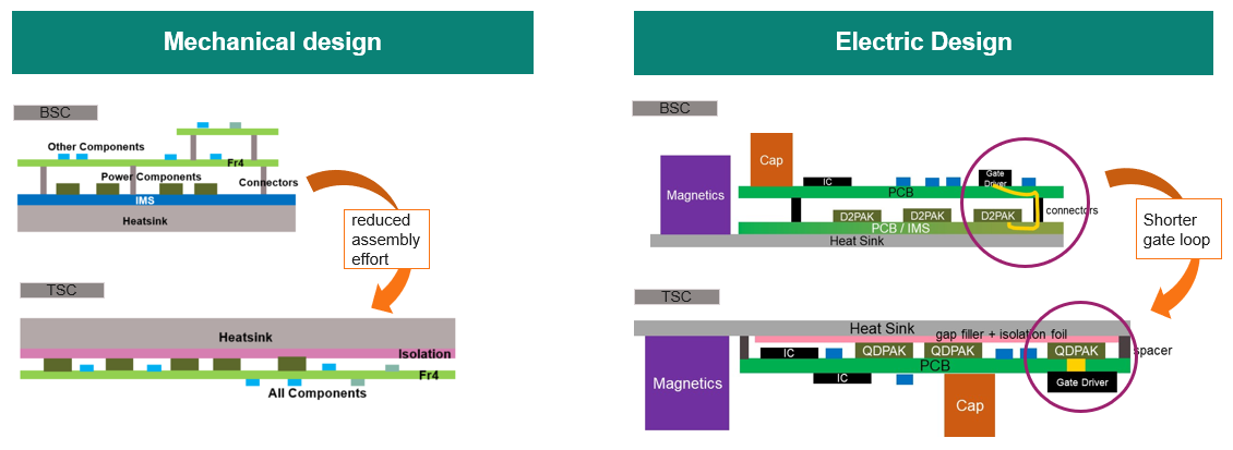
The summary of the advantages of using TSC devices in the application is mentioned below:
System complexity reduction (fewer PCB layers and interconnects) facilitates higher power density and improved reliability
Simplified assembly as well as utilization of both sides of the power PCB is transferred to lower system cost, higher reliability, and power density
IMS board is eliminated reducing the system cost while keeping system Rth low
Lower stray inductance and improved gate control due to shorter loops improve system losses and efficiency.
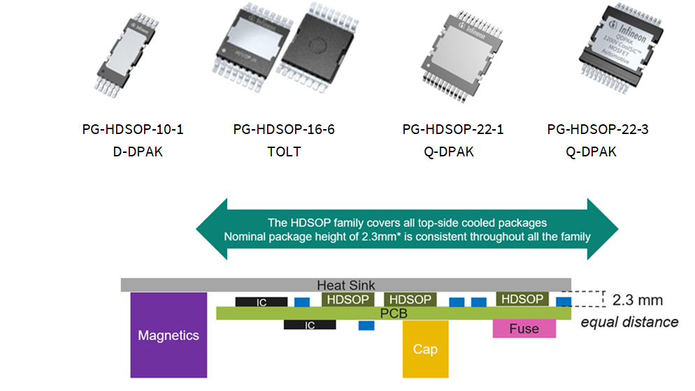
Infineon TSC product portfolio for OBC/DCDC
For different functional blocks of the OBC (PFC, HV-HV DCDC, and HV-LV DCDC) as well as for different system voltages and power ratings, the selection of automotive-qualified products in TSC package is offered by Infineon (
Figure 4
). All HDSOP packages have the same height of 2.3 mm which simplifies the heatsink construction in case different HDSOP packages are mounted on the same PCB.
Figure 4. Product portfolio in TSC packages for HV and LV applications with the same package height
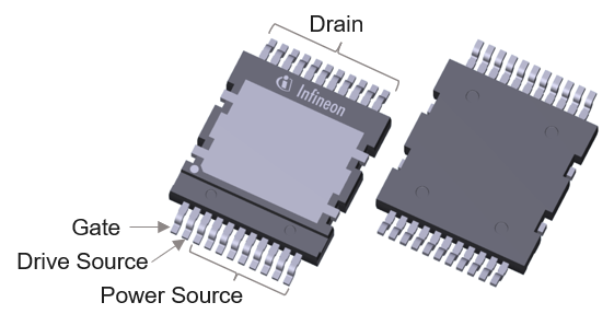
High Voltage Q-DPAK (PG-HDSOP-22-3)
Gen1p CoolSiC™ product family in high voltage version of the Q-DPAK named
PG-HDSOP-22-3
(part of JEDEC standard MO-354) consists of seven R
ds(on)
types: 17, 30, 40, 60, 80, 120 and 160 mOhm. This family addressed the application requests for automated PCB assembly convenience and increased power density. This chapter covers the specific features of the Q-DPAK like increased creepage distance, drive (sense) source pin, improved R
th(j-c)
as well as important thermal considerations and assembly recommendations.
The high-voltage version of Q-DPAK designed for 1200V SiC chips can be easily distinguished by a special groove introduced to increase the creepage distance, as shown in
Figure 5
, including the pin definition.
The heat-dissipating exposed pad on top of the package is connected to the drain potential.
Figure 5. Pin definition of 1200V CoolSiC™ in Q-DPAK (PG-HDSOP-22-3) packag
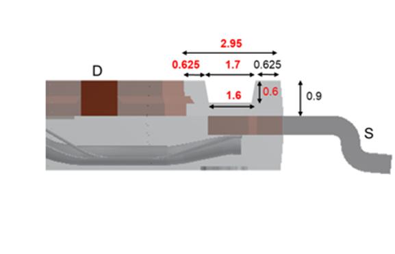
Creepage distance
The creepage distance of more than 4.75 mm is provided by introducing a special groove in the mold compound as shown in
Figure 6
. With the material group I (CTI > 600) used for the mold compound, PG-HDSOP-22-3 is fitting V
rms(max)
of >950V according to IEC60664 for pollution degree 2.
Figure 6. Increasing the creepage distance of the Q-DPAK by implementing a special groove
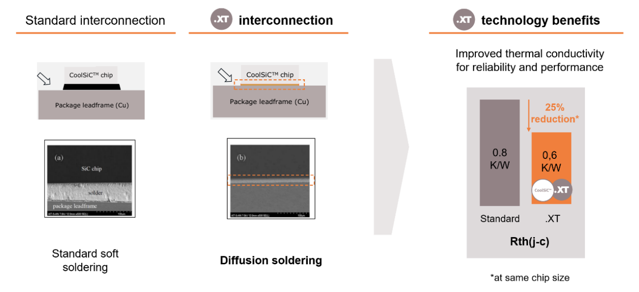
Diffusion soldering and package Rth(j-c)
While a chip shrink helps improve the switching performance, the challenge of dissipating power from the chip increases too. To compensate for the reduction of heat dissipating area while keeping R
th(j-c)
at a minimal level, diffusion soldering die attach technology is implemented. This helps either keep the same R
th(j-c)
for the smaller chip or reduce the R
th(j-c)
by 25% for the chip of the same size (
Figure 7
). Another significant benefit of the diffusion solder die attach is the improved Temperature Cycling (TC) robustness of the device.
Figure 7. Diffusion soldering technology and its impact on the package Rth(j-c)
Drive (sense) source pin
An additional drive (or sense) source pin provides a dedicated connection between the gate driver negative terminal and chip source potential. This helps prevent the voltage drop on the power source bond wires in the gate loop that could potentially distort the gate control signal and increase the switching losses. Additional information on the drive source pin benefits is provided in Section 3.1 of
1
.
Pins with the positive standoff
Q-DPAK is providing a positive standoff up to 150 μm. This means the package body is up to 150 µm higher than the lower edge of the package leads. Details and advantages of the positive standoff are presented in section 3.2 of the application note “Innovative top-side cooled package solution for high-voltage applications. Application considerations for best performance”
2
. An important benefit of the positive standoff for thermal performance is discussed in Section
Application of the gap filler
of this document.
Assembly recommendations
The information on the PG-HDSOP-22-3 package can be found on the package
web page
on the Infineon website. Here the package drawing, PCB footprint (solder mask and stencil aperture), package 3D model, T&R dimensions, and other information can be found. Refer to the application note “Recommendations for board assembly of Infineon transistor outline type packages”
4
containing information on recommended reflow process parameters, Moisture Sensitivity Level (MSL) considerations, and other useful recommendations.
Handling and ESD sensitivity
ESD sensitivity of the MOSFET high-impedance Gate is well known. Any external charge Q connected to the gate generates a voltage equal to Q/C
iss
that can easily exceed the maximum V
GS
value and lead to electric failure in a catastrophic (gate oxide breakdown) of latent (gate oxide degradation) form. SiC MOSFETs having lower input capacitance develop even higher Q/C
iss
voltage values. Standard protection measures have to be taken throughout the logistics and manufacturing process so as not to expose the gate to ESD sources, especially in the case of manual handling. Some useful recommendations can be found in the application note “Designing with power MOSFETs. How to avoid common issues and failure modes ”
5
.
Gate drive
Gate driver considerations
Controlling the SiC power MOSFET gate voltage is one of the important application topics because of its direct influence on both the system performance and MOSFET lifetime and reliability. In this chapter, the following points are discussed:
Selection of gate turn-on and turn-off voltages
Utilizing the advantage of PTO robustness and 0V turn-off
Gate charge QG and requested gate driver output power
Examples of the gate drivers and their connection to MOSFETs
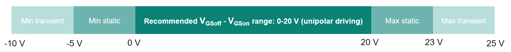
Gate drive voltage
Selection of the right VGSon and VGSoff voltages provides a significant impact on both the system performance and reliability of the device. Infineon Gen1p devices offer circuit designers a flexible range of turn-on and turn-off voltages (
Figure 8
). Recommended VGSon and VGSoff levels for Gen1p chips are 20 V and 0 V respectively. Most datasheet parameters for the Gen1p family are provided at VGS(on)=20 V so a certain parameter derating should be anticipated while driving the gate at VGS(on)=18 V.
Figure 8. Range of allowed and recommended gate voltages
The selection of positive and negative gate-source voltages impacts the long-term behavior of the device. The design guidelines described in the application note “Infineon guidelines for CoolSiC™ MOSFET gate drive voltage window” 3 should be considered to ensure the reliable operation of the device over the planned lifetime.
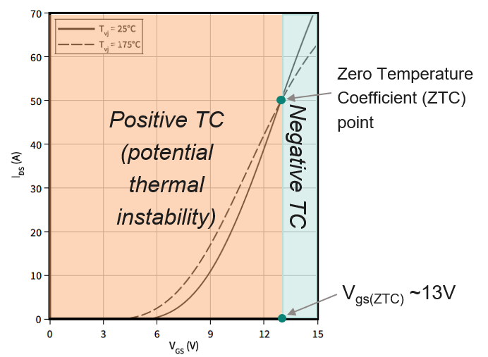
Another important consideration concerning the selection of the VGS(on) is the potential operation in the thermal instability region. This region is characterized by a positive temperature coefficient (TC) where hotter cells of the chip are getting more current which can potentially lead to thermal runaway at the cell level. This is why it is important to ensure in the application the VGS(on) voltage is always above the Zero Temperature Coefficient (ZTC) point. VGS(on) voltage of the ZTC point can be seen in the transfer characteristic in the datasheet (
Figure 9
). Selecting the driver with the under-voltage lock-out (UVLO) protection level above ZTC is critical to avoid operation in the thermal instability region.
Figure 9. Temperature coefficient (TC) and Zero TC point on the transfer curve defining the V GS(on) limit for the thermal instability region
Unipolar gate driving
If a MOSFET susceptible to Parasitic Turn-Ons (PTO) is used in the applications, there are several ways to compensate for the impact, one of which is the negative VGS(off). From the perspective of the gate driver, this means a negative voltage source is needed, requiring several additional components. As discussed earlier in Chapter 2.3 “Avoiding parasitic turn-ons (PTO robustness)” and
1
, Infineon Gen1p technology is PTO-robust and facilitates reliable zero-voltage turn-off without risk of parasitic turn-on. This makes negative gate drive voltage unnecessary and can significantly simplify the gate driver power supply eliminating several passive components and simplifying the transformer.
As explained in
1
even using PTO robust devices like Gen1p CoolSiC, proper attention has to be paid to the selection of RG(off) and RG(on) values, as well as to the routing of critical gate traces on the PCB. This is to minimize the drain-to-gate coupling with unwanted voltage spikes induced in the gate loop during switching transitions.
Gate charge and driver output power
The value of the gate charge QG has been improved in Gen1p. The required gate driver output power Pdrv estimated as Pdrv = QG * FSW * ΔVGS is thus reduced proportionally to QG enabling the gate driver cost reduction as well as helping reduce the power losses and improving system efficiency especially noticeable in a light load operation.
Gate driver example
When designing with Gen1p CoolSiC™ MOSFETs, selecting the right gate driver is important to take full advantage of the capabilities of the device. For half-bridge configuration, the EiceDRIVER™ 2EDR314x dual-channel gate driver family is the simplest and most cost-effective choice. Alternatively, two single-channel gate drivers such as the EiceDRIVER™ 1EDR314xHQ1 family, can be used to provide a more flexible approach, they also have separate source and sink output configurations, making them suitable for single-switch topologies such as the flyback converter.
The EiceDRIVER™ 2EDR314x and 1EDR314x gate drivers offer a range of features, such as:
Suitable UVLO protection (> V GS(ZTC) ) with fast clamping and high propagation delay accuracy
Strong output stage for maximum switching speed and driving devices with higher gate charge
Deadtime control for additional hardware protection and increased reliability
Extended CMTI capability for high switching robustness.
Reinforced isolation according to IEC 60747-17 excluding the need for a separate isolator or secondary MCU
Automotive qualification according to AEC-Q100, making them an ideal match for Gen1p in OBC and DCDC applications.
These features collectively contribute to system-level benefits. The increased switching speed leads to reduced switching losses and smaller passive components, resulting in improved efficiency and decreased cooling requirements. By combining these benefits with the advantages of the QDPAK package, best-in-class power density can be achieved. Furthermore, the tight propagation delay matching allows for shorter deadtimes, which in turn reduces body diode conduction time, leading to a more efficient and reliable system.
Pairing these gate drivers with Gen1p technology also provides cost benefits, including a cheaper driver power supply due to unipolar driving and a reduced bill of materials (BOM) resulting from direct connection with minimum external components. The gate driver is also cost-optimized to cover application requirements without unnecessary extra functions.
Figure 10. Gate driver simplified connection diagram
PCB design consideration
The PCB layout is important for the optimal performance of the gate driver. In high-current, fast-switching applications (such as the OBC), an optimized layout is essential for reliable and robust system operation. A key consideration is the trace length between the gate pin and driver output. The gate driver should be placed as close as possible to the MOSFET to minimize the length of any high-current traces and stray inductance between the driver output pins and the gate of the MOSFET.
Q-DPAK mechanical integration
This chapter covers different aspects of the mechanical integration of devices in Q-DPAK packages into the system, such as improvement of the thermal performance by optimizing the properties of the thermal stack or PCB layout.
Thermal connection to the heatsink
Widely used options for the thermal interface between the heatsink to the PCB with multiple TSC packages are presented in
Figure 11
. Options A and B (gap filler only and gap pad respectively) are easy to use but require special design efforts to guarantee the minimal TIM thickness to ensure the necessary isolation level between the exposed pad (drain potential of the MOSFET) and the heatsink.
Figure 11. Possible options of heatsink attachment to multiple Q-DPAKs on the PCB
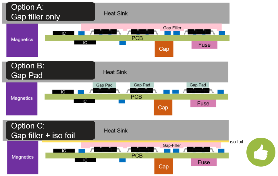
More details on the analysis of achievable isolation level vs remaining TIM thickness are available in
2
. This chapter focuses on option C with gap filler and isolation foil (or the ceramic isolation plate) as the solution providing guaranteed isolation level and highest safety which is of specific importance for 800V OBC systems.
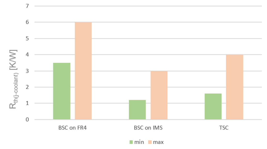
Rth comparison for different heatsink attachment methods
As discussed earlier in Chapter 1.3, the main advantages of the TSC packages are on the system level (less stacked PCBs, avoiding the IMS board, shorter loops with lower parasitic inductance, and more). The system R
th
of the TSC system though can be higher compared to the best BSC+IMS solutions. This is explained by the lower thermal conductivity of the Thermal Interface Material (TIM) attached to the TSC devices (5-8W/mK) compared to the solder layer used to attach BSC devices (35-40W/mK). The comparison of the simulated system R
th
with the 40 mOhm Gen1p chip in BSC and TSC packages with different TIM properties is presented in
Figure 12
. Range of R
th(j-coolant)
for the 40 mOhm chip in BSC and TSC packages with different thermal
The purpose of this comparison is to demonstrate that achievable minimal R
th
(j-coolant)
values for TSC packages are generally higher than those of the BSC on IMS but can get very close with proper thermal stack optimization.
Figure 12. Range of R th(j-coolant) for the 40 mOhm chip in BSC and TSC packages with different thermal stacks (simulation)
The ways of thermal stack optimization for TSC devices are discussed further in this document.
Impact of TIM material and remaining gap filler thickness on Rth(j-h)
Besides the materials selection, the most important optimization path is minimizing the thickness of the thermal interface while maintaining the required isolation properties. The minimal TIM thickness is defined by the height difference between multiple devices mounted on the same PCB. The impact of both TIM conductivity and layer thickness is illustrated in
Figure 13
.
Figure 13. Impact of the TIM material conductivity and the remaining gap filler thickness on Rth(j-h) (simulation)
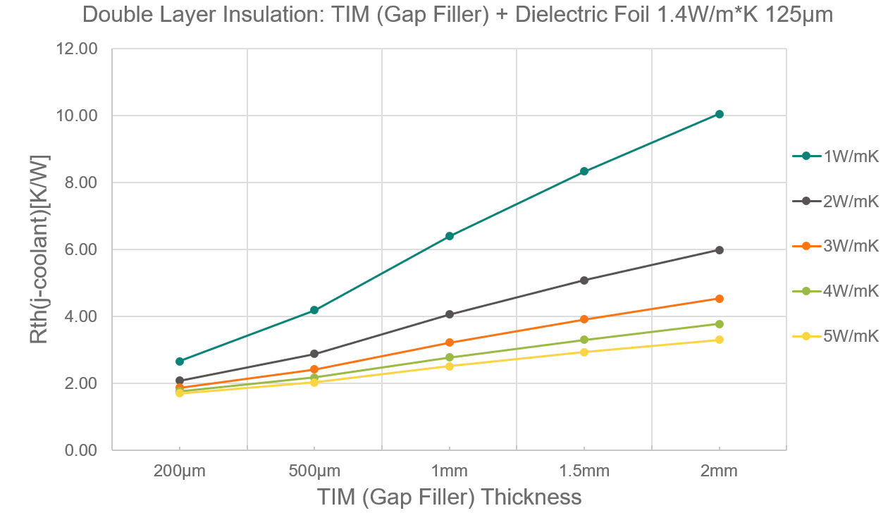
The remaining TIM thickness is defined by the system-level (application) tolerance including the package tolerances plus additional components provided by soldering, PCB warpage, heatsink bending, and more. Minimizing the resulting application tolerance is key for the thermal optimization of the TSC-based system.
Minimizing the remaining TIM thickness
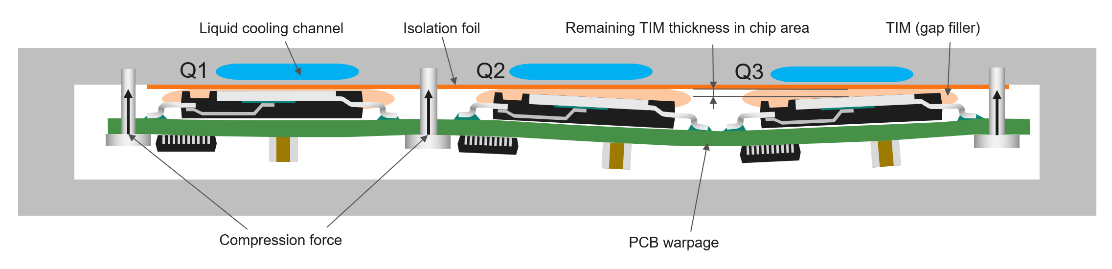
An example of the simplified assembly of the PCB to the heatsink with screws is shown in
Figure 14
. As illustrated in this picture with an exaggeration, the PCB warpage can be expected in the locations where a screw is missing next to either side of the package (for example between Q2 and Q3) which would lead to high remaining TIM thickness and higher Rth of the thermal contact. Fixing this issue with too many screws and associated PCB holes would lead to loss of conducting area in the most critical locations of the conducting planes.
Figure 14. Minimization of the remaining TIM thickness by avoiding PCB warpage
Different aspects of thermal optimization of the system with screw-mounted PCB are discussed in more detail in
2
, this section focuses on the alternative heatsink attach solution as described below.
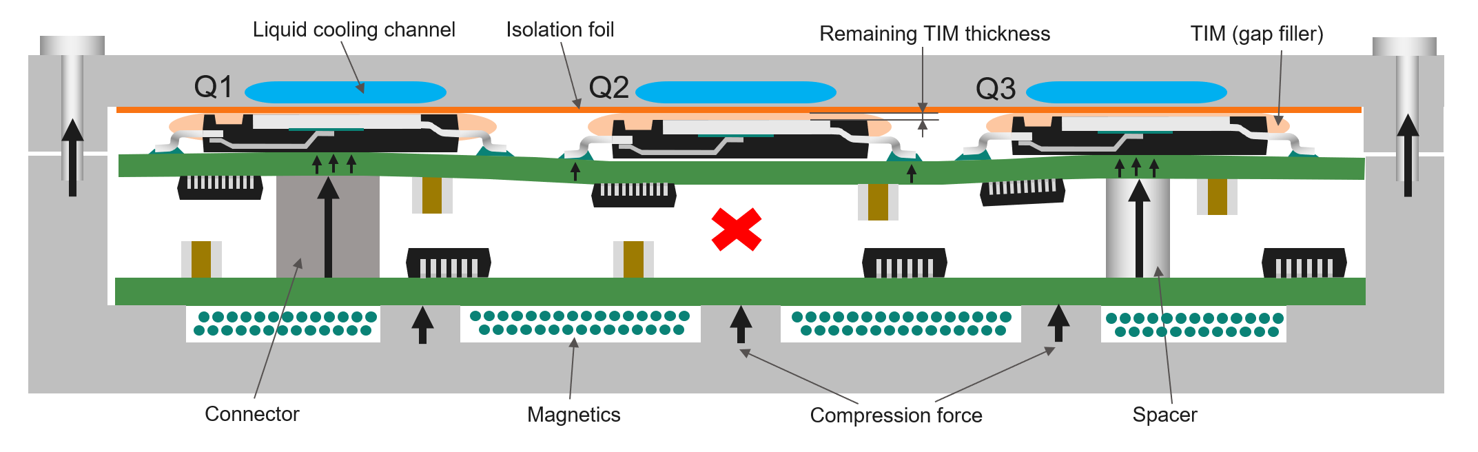
An alternative concept has been utilized in the “Tiny Power Box” design by Silicon Austria Labs GmbH
6
where compression force is provided to the power PCB by spacers and connectors from the back of the PCB. Sufficient hardness of the upper and lower parts of the enclosure was ensured to minimize their bending while providing sufficient compression force to the packages. Ideally, each package should be pressed individually otherwise the devices without a spacer (like Q2 in
Figure 15
with a missing spacer to illustrate the effect) would have higher remaining TIM thickness and respectively higher Rth.
Figure 15. The solution to minimize the remaining TIM thickness is by pressing the PCB from the back
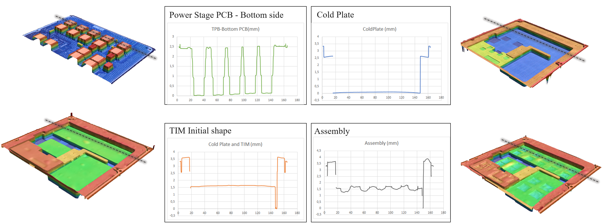
The profile measurement results presented in
Figure 15
were achieved with this solution. Gap pads were used in this design both for gap filling and isolation
6
. As a result, the remaining thickness could not be minimized further due to the minimal thickness of more than 1 mm required for proper isolation. Nevertheless, the important conclusion from this measurement is that the height difference between the “highest” and “lowest” of the five Q-DPAKs (representing the total application tolerance) can be driven down in practice below 300 μm (see “Assembly” plot in
Figure 16
). In the case of using the gap filler plus isolation foil in a similar mechanical setup, the “highest” QDPAK could be pressed all the way to touch the isolation foil (zero remaining TIM thickness), while the “lowest profile” Q-DPAK would have the remaining thickness of 300 μm or less. In such a case, it would be possible to reach the resulting Rth below 2K/W with the materials shown in
Figure 13
for the worst-case (“lowest”) package, or even less with better materials currently available.
Figure 16. Contributions to package height differences of multiple QDPAKs on the PCB attached to the heatsink
According to
6
, comparing the two methods of pressing the TSC package to the heatsink, the following conclusions can be made:
Mounting screws holes on the Power PCB limit the power density goals of the design and interrupt the proper routing by creating breaks in the high-current planes
Connectors and spacers distributed across the back side of the power PCB against Q-DPAK locations provide a homogenous and stiff setup for better control of the worst-case remaining TIM thickness
A carefully planned case design with stiffness walls between sections helps to avoid the bending of large PCB areas, also during thermal cycles.
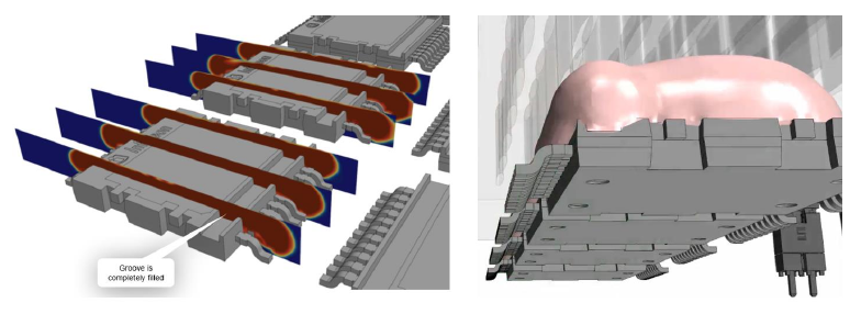
Application of the gap filler
Special attention should be paid to the selection and application of the thermal interface material for the packages with a groove to maintain the creepage path on the package level. Properly dispensed thermal grease is proven to fill the groove without gaps (simulation results presented in
Figure 17
), while the gap pad with ultrasoft material should be selected to reach the same result.
Figure 17. Complete filling of the package groove with a gap filler (simulation)
Applying force on the package
When compression force is applied, the distance between the package and PCB is reduced while leads are acting as springs. With the application of sufficient compression force (around 100N per package), the package almost touches the PCB (
Figure 18
). The initial tolerance of the positive standoff (0…150 μm according to the datasheet) is excluded from the overall application tolerance (
Figure 13
) and only the package tolerance (datasheet package drawing parameter A of ±50 μm) remains as the package contribution to the overall system tolerance.
Figure 18. Distance between the package and PCB before and after compression force application (leads acting as springs)
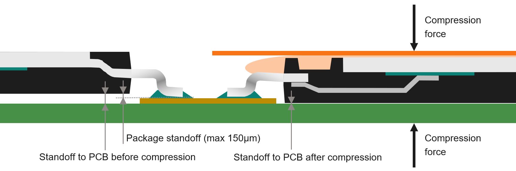
As described in
2
, investigations showed no negative influence on the long-term reliability when using top-side cooling packages with a significant force applied to minimize the remaining TIM thickness. The provided force is absorbed by the leads of the package as they act in a spring-like manner, and the solder joint connections are not negatively influenced during thermal cycling tests
2
.
PCB Layout
As explained in the previous chapters, Q-DPAK offers several features that make the PCB design easier, while also requiring attention to certain topics. Basic recommendations are listed below:
The first and most obvious one is to make use of the symmetrical package design of the Q-DPAK and route the return current path on the PCB lower layer copying the direct path through the MOSFETs and thus minimizing the parasitic inductance of the power loop (
Figure 19
). An array of MLCCs can be used to close the loop.
The gate driver network should be located as close as possible to the Q-DPAK’s gate and driver source pins to minimize parasitic voltages induced on the gate and thus ensure clean on/off levels and transitions.
Figure 19. Example of the low inductive PCB Layout with a short gate loop
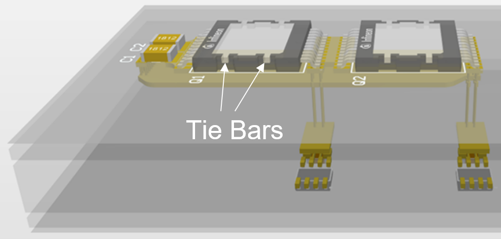
Attention must be paid to the creepage and clearance from the tie bars of the exposed pad to the top layer, if the latter has a high potential difference to drain. This can be achieved for example by routing only drain potential as the top layer under the tie bars, or by providing cuts in these areas matching the creepage/clearance targets.
Conclusion
The optimal combination of the Gen1p chip technology features like low switching losses and PTO robustness together with Q-DPAK package advantages such Top-Side Cooling with low Rth result in the product family perfectly meeting the requirements of modern OBC/DCDC systems with the highest efficiency and power density.
Potential challenges in system design areas such as gate driving, thermal design, and mechanical integration can be successfully addressed by the tips and recommendations explained in this article as well as the referred material.
References
Infineon Application Note “1200-V Gen1p CoolSiC ™ MOSFETs in TO263-7 package for automotive applications”
Infineon Application Note “Infineon guidelines for CoolSiC MOSFET gate drive voltage window”
Infineon Application Note “ Recommendations for board assembly of Infineon transistor outline type packages ”
Infineon Application Note “Designing with power MOSFETs . How to avoid common issues and failure modes “
Technical Article by Recepi I. et al., “Tiny Power Box – Mechanical Investigations for Automotive Very High Power Density Onboard Chargers” . PCIM Europe 2023
Technical Article by Mentin C. et al., “Tiny Power Box - Thermal Investigations for Very High Power Density Onboard Chargers” . Proceedings Therminic 2022
Revision history
Document version | Date | Description of changes |
|---|---|---|
V1.0 | 16.10.2024 | Initial version |
V1.1 | 23.09.2025 | Template update; no content update |