Z8F804051581200 V Gen1p CoolSiC™ MOSFETs in TO263-7 package for automotive applications
About this document
Scope and purpose
This Application Note describes the family of 1200V SiC MOSFETs in the TO263-7 package intended primarily for the On-Board Charger (OBC) systems of Battery Electric Vehicles (BEV) but can also be used in other Automotive applications. The purpose of this document is to introduce and explain the specific features of the family products. Important application topics are covered to help design the system for maximum efficiency and reliability.
Intended audience
This document is intended for circuit design engineers developing Automotive Power Electronics Systems.
Introduction
The new generation of CoolSiC™ MOSFETs in the TO263 7-pin package is a significant addition to the Infineon Automotive SiC MOSFET portfolio offering the best in class switching performance, robustness against parasitic turn-ons as well as improved R
DSon
and R
th(j-c)
. The features of these new devices answer the requests and challenges of the Battery Electric Vehicle (BEV) On-Board Charger (OBC) application for which this product family was initially optimized. We explain in the following chapters:
Specific requirements of the target application (OBC) and how this new family is meeting them
Features of the new generation chip technology including fast switching and parasitic turn-on robustness
Advantages and special features of the package
Topics of device usage such as gate driving or thermal management
On-Board Charger as the Target Application
With the fast Battery Electric Vehicle evolution and growing penetration, the charging speed at residential locations depending on the built-in OBC is a very important use topic. Typical OBC consists of a rectifier PFC and high voltage DC-DC parts. Though OBC parameters vary and different topologies are used for both parts, some general trends can be identified:
Increasing OBC power to 11-22 kW
Increasing power density
The growing interest in bidirectional topologies for supporting V2L (Vehicle to Load), V2H (Vehicle to Home) of V2G (Vehicle to Grid) operation modes and use of controlled switches instead of diodes to enable bidirectional operation
Battery voltage increase to 800 V
Following these trends and requirements we see increasing use of flexible topologies like bidirectional Totem-pole B6 PFC and Dual Active Bridge (DAB) DC-DC for 800 V battery/DC link using 1200 V SiC MOSFETs (
Figure 1
).
Figure 1. Onboard Charger (OBC) topology example: bidirectional B6 Totem-pole PFC (left part) and Dual Active Bridge (DAB) DC-DC (right part)
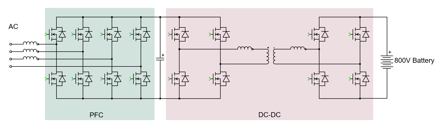
These OBC trends translate to respective requirements for semiconductor switches as OBC’s main building blocks:
Low device capacitances and switching energy as well as better switching control to allow higher frequencies
1200 V V DS voltage class and proper creepage distance to fit 800 V Battery/system voltage
SMT package preferred for increased power density and automated assembly
Optimization of all parameters influencing system cost (including gate driver, cooling system, and passives)
The next chapters explain in more detail how the new Infineon CoolSiC™ MOSFET family helps meet these requirements.
New CoolSiC™ MOSFETs to address OBC application requirements
The new generation of CoolSiC™ MOSFETs in the SMD package code-named “Gen1p” is based on the first generation (Gen1) of SiC MOSFET chip technology. New Gen1p SiC MOSFET family in the TO263-7 package brings the following improvements compared to the Gen1 family in the TO-247 3-pin package:
Compact optimized chip design with improved R DSon * Area FOM
Best in class device capacitances and switching energy
A combination of low C rss /C iss ratio and high V GSth helps avoid parasitic turn-ons
Reduced total gate charge Q gtot for lower driving power/losses
Increased turn-on voltage (V GS = 20 V) for lower R DSon
Advanced diffusion soldering chip mount technology for improved R th(j-c)
Lower package stray inductance for faster and cleaner switching
Source sense (Kelvin) pin for better gate control and reduced switching losses
Increased creepage distance to fit 800 V DC applications without a need for coating
Choice of R DSon options for an optimal fit to application requirements including the only 10 mΩ type in the TO263-7 package currently on the market
These features give the following benefits to the application:
Smaller and cheaper inductors and capacitors due to higher possible switching frequency
Less cooling efforts and smaller heatsinks because of lower switching losses
Higher power density and lower system cost due to the SMD package
Simplified unipolar gate driver made possible by 0 V turn-off with reduced driving power thanks to low Q G
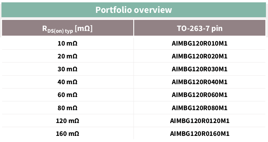
Device portfolio in the TO263-7-12 package
The AIMBG120RxxxM1 family consists of 8 devices with different R
DSon
ratings including the only 10 mΩ type in the TO263-7 package currently available on the market. This choice makes it possible to always find the optimal fit for any combination of conduction/switching losses in a particular OBC application (
Figure 2
). The key advantages of Gen1p chip technology are explained in Chapter
New Chip technology Gen1p
followed by package advantages discussed in Chapter
Package information
.
Figure 2. Family of Infineon CoolSiC™ MOSFETs based on Gen1p chip technology in TO263-7-12 package
New Chip technology Gen1p
Gen1p is the evolution of the first CoolSiC™ MOSFET generation Gen1 and was optimized for the OBC application profile to provide a cost-effective solution while maintaining the reliability and the optimal balance of the key parameters.
Advantages of the Gen1p technology:
Best in class switching performance: low switching losses and device capacitances
Robustness against parasitic turn-ons due to high V GSth and low C rss /C iss
Optimized chip technology for reduced R DSon *Area
V GS(on) = 20 V for lower R DSon for the same chip size
Base metallization material optimized for diffusion soldering for lower R th(j-c)
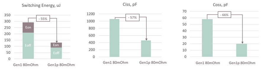
Switching performance
Switching performance is one of the key optimization factors of Gen1p chip technology. Due to reduced chip area (for the same R
DSon
) the device capacitances reduced significantly as can be seen in
Figure 3
for the 80 mΩ parts. Both switch-on and switch-off energy values of Gen1p 80 mΩ device reduced more than 2 times compared to Gen1. This allows for a much higher switching frequency (and thus smaller inductors) while keeping the same switching losses or having much lower switching losses (and less cooling effort) at the same switching frequency. The same implies to the output capacitance C
oss
improved by a factor of 3. Input capacitance C
iss
57% reduction means that less gate driving power is needed to control the MOSFET which translates to a cheaper gate driver and fewer driving losses. Reduced C
rss
and C
rss
/C
iss
ratio help against parasitic turn-ons by minimizing the parasitic transients on Gate induced by high output dv/dt (more on this topic in Chapter
Avoiding parasitic turn-ons
).
Figure 3. Improvements of Gen1p switching parameters compared to the first generation:
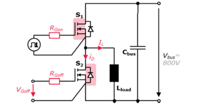
Avoiding parasitic turn-ons
The parasitic turn-on phenomenon is illustrated in
Figure 4
. In the half-bridge circuit, MOSFET S1 turns on while S2 turns off. The fast rise of V
DS
at S2 is inducing a voltage surge at the Gate of S2 via parasitic capacitance C
GD
(also referred to as Miller capacitance or C
rss
). In case this surge is high enough to reach the level of threshold voltage V
GSth
, S2 can reopen letting the shoot-through current flow.
Figure 4. Parasitic turn-on illustration: in a half-bridge circuit (left) S2 just switched off (body diode freewheeling the load current) then S1 is switching on. The parasitic surge is induced at S2 Gate by S2 Drain voltage transient via parasitic capacitance C
GD (C rss ). If the surge level exceeds the V GS(th) , S2 reopens. This leads to an extended tail of the diode reverse recovery current iD(S2) and increased Q rr .

Detailed analysis and measurements presented in Article
1
provide important guidelines for choosing R
Goff
values to avoid parasitic turn-on at VGS(off) = 0 V.
Figure 5
shows the test setup for characterization of the critical R
Goff
value at which S2 still has no parasitic turn-on while S1 is switching on. R
Gon
value is setting the dv/dt generated by S1 turn-on.
Figure 5. Test setup for characterizing the critical gate resistance R
Goff . S2 is switched and kept off by R Goff then S1 is switched on. R Gon sets the dv/dt of the transition.
The criterion of the parasitic turn-on in this measurement is Q
rr
increase by 10% (illustrated by a yellow curve in
Figure 6
left). It was investigated at which maximum R
Goff
value no parasitic turn-on was observed (this R
Goff
value is called “critical” and presented on Y-axis in
Figure 6
right). Critical values were assessed for different R
Gon
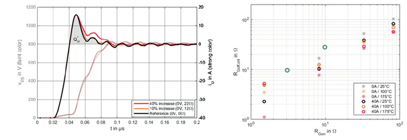
(axis X) at different junction temperatures (25°C, 100°C, and 175°C) and load conditions (0 A or 40 A).
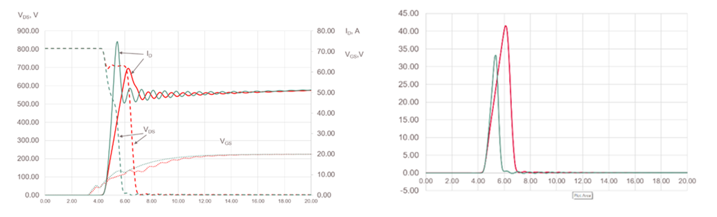
Figure 6. Left: the criterion of a parasitic turn-on is defined as “Q rr
increase by 10%” (waveform in orange strong color) related to reference waveform at R Goff =0Ω (black). Right: critical (maximum) values of R Goff at which no parasitic turn-on takes place (Y-axis). The X-axis represents values of R Gon setting the transition dv/dt. Green dots are results of AIMBG120R80M1 measurement at 175°C and 10A.
Two key parameters define how much MOSFET is susceptible to parasitic turn-on conditions:
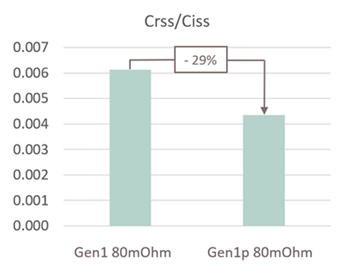
C GD /C GS (also referred to as C rss /C iss ) ratio defines the level of parasitic VGS surge induced by V DSr transient, and C GD /C GS is improved in Gen1p significantly ( Figure 7 )
V GSth (higher V GSth means lower chance for VGS surge to turn on the MOSFET)
Figure 7. The C rss /C iss ratio of Gen1p was improved by 29% compared to Gen1. This reduced the parasitic transition of V DS voltage to the Gate.
The combination of high V
GSth
and reduced C
GD
/C
GS
(or C
rss
/C
iss
) ratio of Infineon Gen1p chip technology leads to higher critical gate resistance values (green dots in
Figure 6
). This gives more flexibility to R
Goff
selection which allows for wider control over commutation speed while maintaining the reliable switch-off with 0V VGS(off). Zero gate voltage turn-off makes simpler unipolar gate driving possible as described in section
Unipolar gate driving
.
Package information
Providing the new Gen1p in a Surface Mount Technology (SMT) package answered the application request for increased system power density and an easier PCB assembly process. We will discuss in this Chapter the following specific features of the TO263-7-12 package used for this product family like Sense (Kelvin) Source pin, increased creepage distance, improved R
th(j-c)
thanks to chip diffusion soldering as well as important thermal considerations and assembly recommendations.
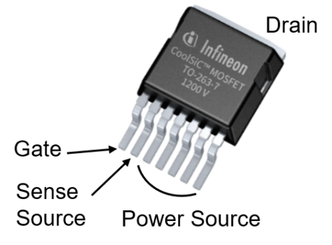
Sense (Kelvin) Source pin
Additional sense Source pin (pin 2 in
Figure 8
) provides a dedicated connection between the Gate driver negative terminal and chip Source potential.
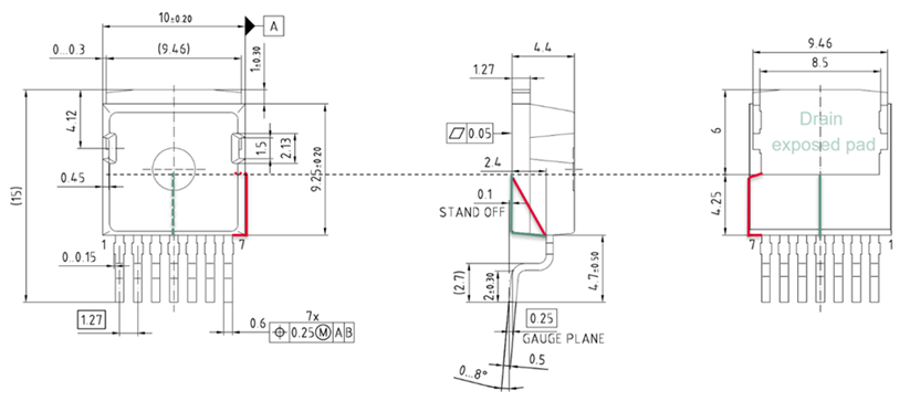
Figure 8. Pin designation of TO263-7-12 package
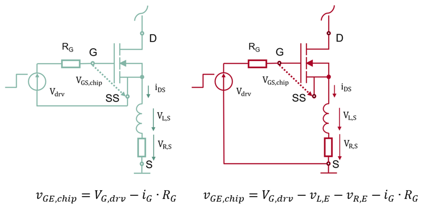
This allows avoiding the distortion of Gate control voltage (V
GS, chip
in
Figure 9
) caused by voltage drop on internal power Source bond wire inductance and resistance (V
L,S
and V
R,S
in
Figure 9
) at high i
DS
currents.
Note:
Driving the Gate with reference to Sense Source is the only recommended option.
Figure 9. Gate drive connection options with reference to: - Sense Source pin SS (left picture, recommended) - Power Source S (right, not recommended)
Simulated switching curves in
Figure 10
show the significant difference in switching behavior as well as switching losses for these driver connection options.
Figure 10. Simulated switching curves and losses with the Gate driver referenced to Sense Source (green, recommended) vs Power Source (red, not recommended)
Creepage distance
In the design of the TO263-7-12 package, the optimal balance is found between the thermal performance set by the leadframe’s exposed pad area and the creepage distance along the package surface from the Source leads to the Drain pad. As a result, the highest on the market (for the TO263-7 package) creepage distance of 5.89 mm is achieved (the shortest creepage paths along the package are shown in
Figure 11
). This distance value allows for meeting the 800V system creepage requirements without a need for PCB coating (according to IEC 60664-1 material group II only 5.6mm creepage is required for the 800 V system).
Figure 11. Shortest creepage paths on TO263-7-12 package surface
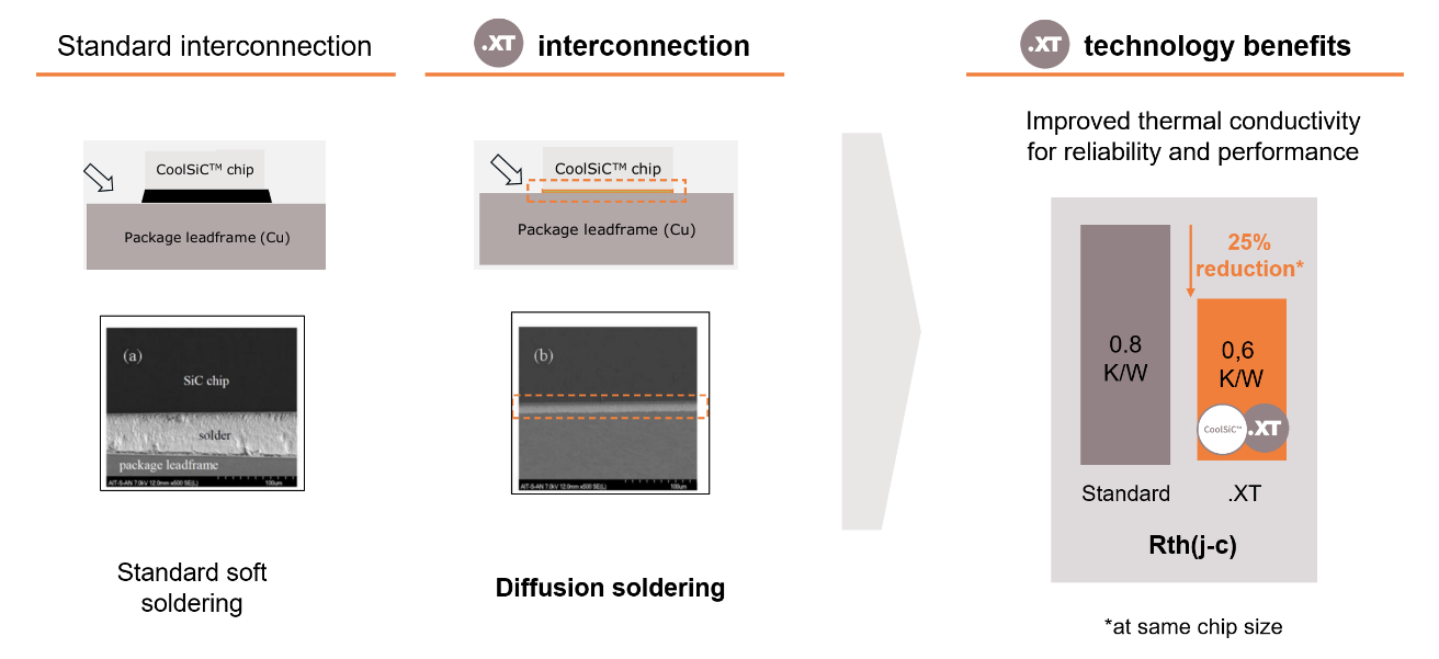
Improved Rth(j-c)
While reducing the chip size helps improve the R
DSon
- Area FOM as well as switching performance, the challenge of dissipating power from the chip increases respectively. To compensate for the reduction of power dissipating area and keep R
th(j-c)
at a minimal level the diffusion soldering chip mount technology was implemented. This helped to either keep the same R
th(j-c)
for the smaller chip with the same R
DSon
or to reduce the R
th(j-c)
by 25% for the chip of the same size (
Figure 12
).
Figure 12. Diffusion soldering technology and its impact on Rth(j-c)
As the heat dissipation from the package to the heatsink through PCB remains the challenge for all SMD Bottom-Side-Cooled (BSC) packages, this topic requires special attention and is discussed further in
Thermal considerations
.
Thermal considerations
Maximum junction temperature must be never exceeded even under the worst application conditions (max losses at highest ambient temperature). As both R DSon and switching energy E tot are increasing with T vj , the correct values of “hot” (at target maximum T vj .) R DSon and E tot should be used for calculations.
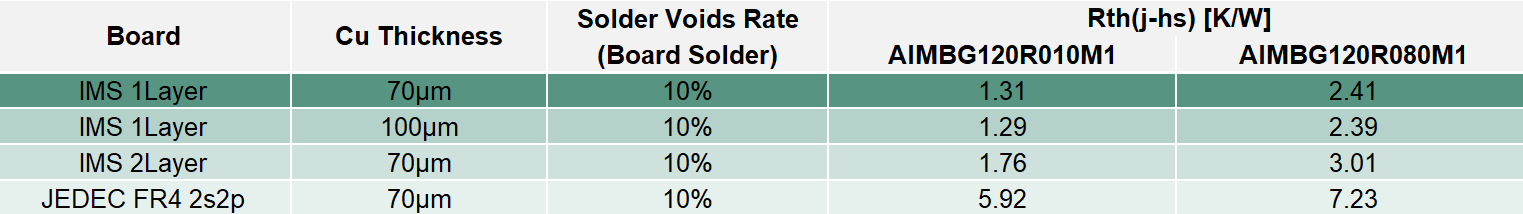
Using IMS (Insulated Metal Substrate) board is highly recommended for optimal thermal management keeping junction temperature below the designated level. Results of the thermal simulations with 10 mΩ part AIMBG120R010M1 (biggest chip size) and 80 mΩ AIMBG120R080M1 indicate the thermal performance that can be reached for these types with different types of PCBs (
Figure 13
). Simulation is done with 20 W power losses, 25°C ambient temperature, and a 10% solder void rate. The resulting values of thermal resistance from junction to heatsink via PCB demonstrate that using an IMS board gives a significant advantage in Rth(j-hs) reduction.
Figure 13. Comparison of thermal resistance junction to heatsink Rth(j-hs) for AIMBG120R010M1 and AIMBG120R080M1 mounted on Insulated Metal Substrate (IMS) and FR4 PCBs
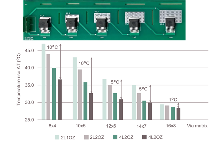
In case FR4 PCB is used (e.g. for cost considerations), the thermal connection from the device package to the bottom copper plane is becoming key to thermal performance. It is usually performed by plated through-hole vias in the board. Thermal and electrical analysis and/or testing together with a proper board assembly design procedure are recommended to determine the optimal PCB parameters and the number of vias needed. Application note “Thermal Measurement for D2PAK on PCB”
4
provides the detailed analysis of measurements made on a real prototype board with different combinations of PCB type (2- or 4-layer, copper thickness), footprint area as well as via matrix setups (example part of the PCB on
Figure 13
and respective measurement results on
Figure 14
).
Figure 14. Test board for comparing TO263-7 footprints on FR4 PCB with different configurations of layers, copper thickness, and a via matrix setup (PCB on top). The graph represents respective values of temperature rise. Results show the impact on thermal performance by thermal vias (8x4 to 16x8 matrix), copper layers (2L or 4L), and copper layer thickness (1OZ or 2OZ).
Assembly recommendations
Actual updated information about the TO263-7-12 package can be found on the
dedicated page
on the Infineon website. This includes detailed package drawings, soldering PCB footprint, and other information. Application note “Recommendations for board assembly of Infineon transistor outline type packages”
4
covers such topics as recommended reflow process parameters, Moisture Sensitivity Level (MSL) considerations, and other useful recommendations.
Gate drive
Gate driver considerations
Controlling the SiC power MOSFET Gate voltage is one of the
important application topics because of its direct influence on both the system
performance and MOSFET lifetime and reliability. In this Chapter we discuss:
Selection of gate turn-on and turn-off voltages
Utilizing the advantage of the 0V switching
Gate charge QG and requested gate driver output power
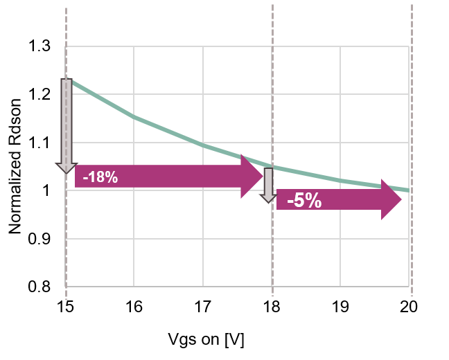
Gate drive voltage
Selection of the right V
GSon
and V
GSoff
voltages provides a significant impact on both the system performance and reliability of the device. Recommended V
GSon
and V
GSoff
levels for Gen1p chips are 20 V and 0 V respectively. V
GSon
increase from 15 V to 18 V gives an R
DSon
reduction of 18% and a value of 20 V provides the lowest R
DSon
with an additional 5% improvement as shown in
Figure 15
. Please note that most datasheet parameters for the Gen1p family are provided at V
GS(on)
= 20 V while driving the gate at V
GS(on)
= 18 V would require a respective parameter derating.
Figure 15. The graph illustrates the R ds(on) reduction with increased V gs(on) value: by 18% with V gs(on) changing from 15 V to 18 V and an additional 5% from 18 V to 20 V
V
GS(off)
value of 0 V is recommended as discussed in
Avoiding parasitic turn-ons
. V
GS
voltages exceeding the recommended range are only allowed as short spikes and should be minimized to ensure the maximum device lifetime. Maximum values of VGS peak values provided in the datasheet at the specified switching frequency and duty cycle give a good guideline.
Note:
The selection of positive and negative gate-source voltages impacts the long-term behavior of the device. The design guidelines described in the Application Note “Infineon guidelines for CoolSiC™ MOSFET gate drive voltage window”2 must be considered to ensure the reliable operation of the device over the planned lifetime.
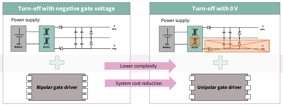
Unipolar gate driving
Using MOSFETs susceptible to parasitic turn-on normally required the negative bias of the gate voltage to ensure the reliable turn-off state without the risk of parasitic turn-on gate voltage induced by Miller capacitance. From the gate driver's perspective, this means a negative voltage source is needed, requiring several additional components (
Figure 16
left side).
As discussed earlier in Chapter
Switching performance
, Infineon Gen1p technology facilitates reliable zero gate voltage turn-off without risk of parasitic return-on. This makes negative gate drive voltage unnecessary and can significantly simplify the gate driver power supply saving a Schottky diode, two capacitors, and a Zener diode plus simplifying the transformer (
Figure 16
right side).
Figure 16. Unipolar gate drive possibility with reliable 0V turn-off helps simplify the gate driver, reduce component count and costs
Note:
An additional advantage of unipolar gate driving is better stability of the MOSFET threshold voltage V GS(th) during the lifetime because negative VGS voltage may lead to the unwanted drift of the threshold voltage V GS(th) value during the device lifetime. In case negative V GS(off) is still intended in the application the following article is recommended to learn more about V GS(th) drift phenomenon in 2.
As explained in
1
even devices less susceptible to parasitic turn-on like Gen1p MOSFETs require in unipolar gate drive mode careful consideration of R
G(off)
value as well as PCB layout of critical gate traces to ensure no Drain-Gate capacitance is added externally. Sometimes using the driver with Miller clamp functionality can still be considered to get an extra safety margin.
Gate charge and driver output power
The value of the Gate charge Q
G
has been improved in Gen1p technology as shown in
Figure 17
.
Figure 17. Gen1p technology Gate charge reduction (Q G is calculated for V GS swing from 0 to 18 V for Gen1 and from 0 V to 20 V for Gen1p)
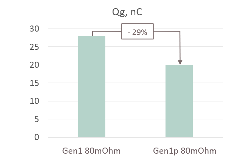
The required Gate driver output power estimated as P
drv
= Q
G
* F
SW
* ΔV
GS
is thus reduced proportionally to Q
G
enabling the Gate driver cost reduction as well as helping reduce the power losses and improve system efficiency especially noticeable in a light load operation.
ESD sensitivity
Note:
ESD sensitivity of the MOSFET high-impedance Gate terminal is well known. Any external charge Q connected to the Gate generates a gate voltage Q/C iss that can easily exceed the maximum V GS value and lead to electric failure in a catastrophic (gate oxide breakdown) of latent (gate oxide degradation) form. SiC MOSFETs optimized for faster switching and having lower C iss develop even higher Q/C iss voltage values. Special measures need to be taken throughout the logistics and manufacturing process to ensure that the Gate terminal is never accidentally connected to potentially dangerous ESD sources. Some useful recommendations can be found in 5 .
References
K. Sobe, T. Basler and B. Klobucar, “ Characterization of the parasitic turn-on behavior of discrete CoolSiC™ MOSFETs” , PCIM Europe 2019; International Exhibition and Conference for Power Electronics, Intelligent Motion, Renewable Energy and Energy Management, 2019, pp. 1-7. ISBN:978-3-8007-4938-6
Infineon Application Note “Infineon guidelines for CoolSiC™ MOSFET gate drive voltage window”
Infineon Application Note “Recommendations for board assembly of Infineon transistor outline type packages ”.
Infineon Application Note AN-2021-02 “Thermal Measurement of D2PAK on PCB ”
Revision history
Document version | Date | Description of changes |
|---|---|---|
Rev. 0.11 | 2022-12-13 | Initial release |
Rev. 1.0 | 2025-09-22 | Template update; no content update |