KIT_PSE84_EVAL PSOC™ Edge E84 Evaluation Kit guide
About this document
Scope and purpose
This document serves as a guide for using the KIT_PSE84_EVAL PSOC™ Edge E84 evaluation kit. The document explains the kit operation, describes the out-of-the-box (OOB) example and its operation, and provides hardware details of the board.
Intended audience
This evaluation board is intended for PSOC™ Edge E84 users to familiarize with the MCU and connectivity devices. This board is intended to be used under laboratory conditions.
Reference documents
This user guide should be read in conjunction with the following documents:
Important notice
“Evaluation Boards and Reference Boards” shall mean
products embedded on a printed circuit board (PCB) for demonstration and/or
evaluation purposes, which include, without limitation, demonstration, reference
and evaluation boards, kits and design (collectively referred to as “Reference
Board”).
Environmental conditions have been considered in
the design of the Evaluation Boards and Reference Boards provided by Infineon
Technologies. The design of the Evaluation Boards and Reference Boards has been
tested by Infineon Technologies only as described in this document. The design
is not qualified in terms of safety requirements, manufacturing and operation
over the entire operating temperature range or lifetime.
The Evaluation Boards and Reference Boards provided
by Infineon Technologies are subject to functional testing only under typical
load conditions. Evaluation Boards and Reference Boards are not subject to the
same procedures as regular products regarding returned material analysis (RMA),
process change notification (PCN) and product discontinuation (PD).
Evaluation Boards and Reference Boards are not
commercialized products, and are solely intended for evaluation and testing
purposes. In particular, they shall not be used for reliability testing or
production. The Evaluation Boards and Reference Boards may therefore not comply
with CE or similar standards (including but not limited to the EMC Directive
2004/EC/108 and the EMC Act) and may not fulfill other requirements of the
country in which they are operated by the customer. The customer shall ensure
that all Evaluation Boards and Reference Boards will be handled in a way which
is compliant with the relevant requirements and standards of the country in
which they are operated.
The Evaluation Boards and Reference Boards as well
as the information provided in this document are addressed only to qualified and
skilled technical staff, for laboratory usage, and shall be used and managed
according to the terms and conditions set forth in this document and in other
related documentation supplied with the respective Evaluation Board or Reference
Board.
It is the responsibility of the customer’s
technical departments to evaluate the suitability of the Evaluation Boards and
Reference Boards for the intended application, and to evaluate the completeness
and correctness of the information provided in this document with respect to
such application.
The customer is obliged to ensure that the use of
the Evaluation Boards and Reference Boards does not cause any harm to persons or
third party property.
The Evaluation Boards and Reference Boards and any
information in this document is provided "as is" and Infineon Technologies
disclaims any warranties, express or implied, including but not limited to
warranties of non-infringement of third party rights and implied warranties of
fitness for any purpose, or for merchantability.
Infineon Technologies shall not be responsible for
any damages resulting from the use of the Evaluation Boards and Reference Boards
and/or from any information provided in this document. The customer is obliged
to defend, indemnify and hold Infineon Technologies harmless from and against
any claims or damages arising out of or resulting from any use thereof.
Infineon Technologies reserves the right to modify
this document and/or any information provided herein at any time without further
notice.
Safety precautions
Note:
Please note the following warnings regarding the hazards associated with development systems
 | Caution: The evaluation or reference board contains parts and assemblies sensitive to electrostatic discharge (ESD). Electrostatic control precautions are required when installing, testing, servicing or repairing the assembly. Component damage may result if ESD control procedures are not followed. If you are not familiar with electrostatic control procedures, refer to the applicable ESD protection handbooks and guidelines. |
Introduction
The PSOC™ Edge E84 evaluation kit enables you to evaluate and develop your applications using the
PSOC™ Edge E84 series MCU
(called “PSOC™ E84”) and a multitude of on-board multimedia, Machine Learning (ML), and connectivity features like MIPI-DSI displays, audio interfaces, and AIROC™ Wi-Fi & Bluetooth® combo-based connectivity modules.
PSOC™ E84 is an ultra-low-power PSOC™ device specifically designed for ML, wearables, and IoT products like smart thermostats, smart locks, smart home appliances, and industrial HMI. Refer to
datasheet
for detailed feature description of PSOC™ E84 MCU.
The evaluation kit carries a PSOC™ E84 MCU on a SODIMM-based detachable SOM board connected to the baseboard. The MCU SOM also has 128 Mb of QSPI flash, 1Gb of Octal flash, 128 Mb of Octal RAM, PSOC™ 4000T as CAPSENSE™ co-processor, and on-board AIROC™ Wi-Fi & Bluetooth® combo.
The baseboard has M.2 interface connectors for interfacing external radio modules based on AIROC™ Wi-Fi & Bluetooth® combos and external memory interfaces. The base-board features an on-board programmer/debugger (KitProg3), ETM/JTAG/SWD debug headers, a custom display capacitive touch panel connector, an R-Pi compatible MIPI-DSI connector and a MIPI-DSI custom display connector, analog and PDM microphones, a headphone connector, a speaker, USB host Type-A and USB device Type-C connectors, an RJ45 Ethernet connector, an M.2 (B-key) memory interface and an M.2 (E-key) radio interface, Infineon’s Shield2Go interface, MikroElektronika's mikroBUS compatible headers, a 6-Axis IMU sensor, a 3-axis magnetometer, a microSD card holder, CAPSENSE™ buttons and slide, user LEDs, and user buttons. The MCU power domain supports 2.7 V, 3.3 V, and 4.2 V operating voltages, and the peripheral power domain supports 1.8 V and 3.3 V operating voltages.
You can use ModusToolbox™ software to develop and debug your PSOC™ E84 MCU projects.
ModusToolbox™ software
is a set of tools that enable you to integrate these devices into your existing development methodology.
Kit contents
The following are kit contents:
PSOC™ Edge E84 evaluation kit
PSOC™ Edge E8 base board
PSOC™ Edge E84 SOM (MOD_PSE84_SOMS2)
USB Type-C to Type-C cable
4.3 inch display with capacitive touch screen
0.3 MP USB camera Module with USB Type-A cable
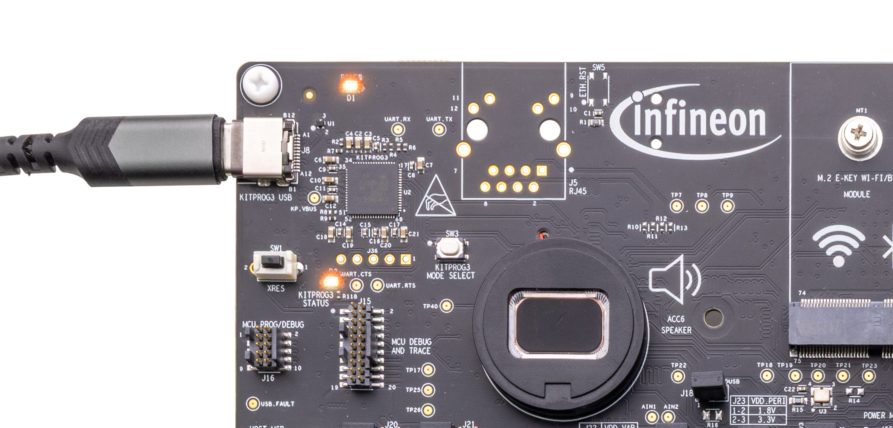
Figure 1.
Kit contents
Inspect the contents of the kit; if you find any parts missing, go to the
Infineon Support Page
.
Getting started
This guide will help you to get acquainted with PSOC™ Edge E84 evaluation kit:
The Kit operation chapter describes the major features of the PSOC™ E84 MCU evaluation board and functionalities such as programming, debugging, and the USB-UART and USB-I2C bridges
The Hardware chapter provides a detailed hardware description, kit schematics, and the Bill of Materials (BOM). This chapter also gives info on reworks required on kit to use alternate functions
Application development using PSOC™ E84 MCU Evaluation Kit is supported in ModusToolbox™ software. ModusToolbox™ software is a free development ecosystem that includes the Eclipse IDE for ModusToolbox™ software and the PSOC™ E84 SDK with PSOC™ E84 MCU. Using ModusToolbox™ software, you can enable and configure device resources, middleware libraries write C or assembly source code, program and debug the device. You can download the software from ModusToolbox™ home page . See the ModusToolbox™ software installation guide for additional information
There are wide range of code examples to evaluate the PSOC™ E84 MCU Evaluation Kit. These examples help you familiarize PSOC™ E84 MCU and create your own design. These examples can be accessed through ModusToolbox™ Project Creator tool. Alternatively, you can also visit Infineon Code examples for ModusToolbox™ software page to access these examples
Board details
The PSOC™ E84 Evaluation Kit has the following features:
PSOC™ E84 MCU - PSE846GPS4DBZC4A, See the device datasheet for more details
Onboard AIROC™ Wi-Fi & Bluetooth® combo - CYW55513IUBGT
PSOC™ 4000T as CAPSENSE™ coprocessor
Display interfaces for custom capacitive touch panels, R-Pi compatible MIPI-DSI displays, and MIPI-DSI custom displays
Analog and PDM microphones, a headphone connector provision and an onboard speaker for audio applications
6-axis accelerometer and gyroscope IMU and a 3-axis magnetometer
Connectors for high-speed connectivity interfaces, such as Ethernet and USB
KitProg3 onboard SWD programmer/debugger, USB-UART, and USB-I2C bridge functionality
128 Mbit external Quad SPI flash, 1 Gbit external Octal flash, and 128 Mbit Octal RAM provide fast, expandable memory for data and code
M.2 (B-key) interface for external memory devices
M.2 (E-key) interface for radio connectivity modules
CAPSENSE™ touch-sensing slider (5 elements), two buttons, and proximity sense are based on self-capacitance (CSD) and mutual-capacitance (CSX) based sensing
Add-on board interface compatible with mikroBUS by MikroElektronika
Add-on board interface compatible with Infineon’s Shield2Go
Add-on board interface compatible with Arduino UNO R3
Selectable input supply voltages of 1.2 V, 3.3 V, and 4.2 V for the PSOC™ E84 MCU
Selectable input supply voltages of 1.8 V or 3.3 V for the onboard peripherals
Three user LEDs, two user buttons, and a reset button for the PSOC™ E84 MCU
A potentiometer that can be used to simulate analog sensor output
Figure 2.
Baseboard with SOM connected - Top View
Baseboard Power LED (
D1
)
KitProg3 Program/Debug USB Type-C connector (
J8
)
PSOC™ 5LP-based KitProg3 programmer and debugger (CY8C5868LTI-LP039,
U2
)
Reset button (
SW1
)
KitProg3 status LED (
D2
)
PSOC™ Edge E84 MCU ETM/JTAG debug and trace header (
J15
)
PSOC™ Edge E84 MCU 10-pin SWD/JTAG program and debug header (
J16
)
Alternative serial interface configuration headers (
J20
,
J21
)
PSOC™ Edge E84 MCU USB host Type-A connector (
J27
)
USB Type-C Power Delivery (PD) fault LED (
D6
)
Custom display capacitive touch panel connector (
J37
)
PSOC™ Edge E84 MCU USB device Type-C connector (
J30
)
External power supply VIN connector (
J31
)
PSOC™ Edge E84 MCU user buttons (
SW2
,
SW4
)
M.2 (B-key) memory interface connector (
J29
)
128 Mbit Octal-SPI HYPERRAM™ (S70KS1283GABHI020,
U12
)
Processor system-on-module (SoM) 260-pin SODIMM connector (
J28
)
CYW55513 tri-band (Wi-Fi & Bluetooth®) combo radio (
U3
) section
Processor System on Module (SoM) power LED (
D3
)
1 Gbit Octal-SPI NOR flash (S28HS01GTGZBH1030,
U10
)
2
128 Mbit Quad-SPI NOR flash (S25FS128SAGMFB100,
U11
)
MIPI-DSI custom display connector (
J38)
1
PSOC™ Edge E84 MCU (PSE846GPS4DBZC4A,
U1
)
PSOC™ 4000T CAPSENSE™ co-processor (
U9
)
2
Raspberry Pi-compatible MIPI-DSI display connector (
J39
)
1
3-axis magnetometer (BMM350,
U4
)
Raspberry Pi compatible display capacitive touch connector (
J41
)
1
Linear potentiometer (
R34
)
Analog microphones (IM73A135V01XTSA1,
U36
and
U37
)
1
User LEDs (
D3
,
D4
,
D5
)
Thermistor (
TH1
)
CAPSENSE™ buttons and slider (
CSB1
,
CSB2
,
CSS1
)
Boot configuration switch (
SW6
)
Proximity sense connector (
J19
)
I/O headers compatible with Arduino UNO R3 (J2, J3, J4)
Alternative serial interface I/O header (
J14
)
Power header compatible with Arduino UNO R3 (
J1
)
PSOC™ Edge E84 MCU expansion I/O headers (
J6
,
J7
,
J40
)
3
MicroSD card holder (
J35
)
1
Infineon's Shield2Go interface headers (
J10
,
J12
)
3
PDM microphones (IM72D128V01XTMA1,
U7
and
U8
)
1
mikroBUS-compatible headers by MikroElektronika (
J9
,
J17
)
3
Extended I2S header (
J11
)
3
6-axis accelerometer and gyroscope IMU (BMI270,
U5
)
M.2 (E-key) radio interface connector (
J13
)
PSOC™ Edge E84 MCU power selection/monitoring headers (
J18
,
J22
,
J23
,
J24
,
J25
,
J26
)
Headphone connector (
J34
)
3
Speaker (
ACC6
)
RJ45 Ethernet MagJack connector (
J5
)
3
KitProg3 programming mode selection button (
SW3
)
Figure 3.
PSOC™ Edge E84 board pin out details
PSOC™ Edge E84 I/O | Header | Function | Logic level |
|---|---|---|---|
P3[0] | J6.5 | I3C SCL | 1.8 V |
P3[1] | J6.4 | I3C SDA | 1.8 V |
P7[0] | J40.1 | GPIO | 1.8 V |
P7[1] | J40.2 | GPIO | 1.8 V |
P8[0] | J3.10, J17.5, J10.5 | I2C SCL pin compatible with Arduino/mikroBUS by MikroElektronika/Infineon's Shield2Go | 1.8 V (MCU side), VDD_PERI (1.8 V/3.3 V) (header side) |
P8[1] | J3.9, J17.6, J10.4 | I2C SDA pin compatible with Arduino/mikroBUS by MikroElektronika/Infineon's Shield2Go | 1.8 V (MCU side), VDD_PERI (1.8 V/3.3 V) (header side) |
P8[2] | J2.2 | GPIO0 for motor control/GPIO | 1.8 V |
P8[3] | J6.1 | User button 1 with hibernate wakeup capability, GPIO | 1.8 V |
P8[4] | J6.3 | I2C interrupt 2 pin connected to magnetometer sensor, GPIO | 1.8 V |
P8[7] | J6.2 | User button 2 with hibernate wakeup capability, GPIO | 1.8 V |
P9[0] | J14.1 | Alternate serial interface pin (SPI Chip Select/UART RTS) | 1.8 V |
P9[1] | J14.2 | Alternate serial interface pin (SPI MISO/UART CTS) | 1.8 V |
P9[2] | J14.3 | Alternate serial interface pin (SPI MOSI/I2C SDA/UART TX) | 1.8 V |
P9[3] | J14.4 | Alternate serial interface pin (SPI CLK/I2C SCL/UART RX) | 1.8 V |
P10[4] | J7.11 | Bluetooth® host wakeup pin, GPIO | 1.8 V |
P10[5] | J4.7, J10.8 | D6 pin compatible with Arduino, INT/GPIO3 pin of Infineon's Shield2Go | 1.8 V |
P10[7] | J3.2 | D9 pin compatible with Arduino | 1.8 V |
P11[0] | J11.1 | Extended I2S interface TX SCK | 1.8 V |
P11[1] | J4.8, J10.9 | D7 pin compatible with Arduino, PWM/GPIO4 pin of Infineon's Shield2Go | 1.8 V |
P11[2] | J11.2 | Extended I2S interface TX SD | 1.8 V |
P11[3] | J4.4, J17.2, J12.3 | D3 pin compatible with Arduino, INT pin compatible with mikroBUS, RST/GPIO2 pin of Infineon's Shield2Go | 1.8 V |
P11[4] | J11.3 | Extended I2S interface RX SCK | 1.8 V |
P11[5] | J4.6, J12.4 | D5 pin compatible with Arduino, GPIO1 pin of Infineon's Shield2Go | 1.8 V |
P11[6] | J11.4 | Extended I2S interface RX SD | 1.8 V |
P11[7] | J4.5, J17.1 | D4 pin compatible with Arduino, PWM pin compatible with mikroBUS | 1.8 V |
P13[0] | J2.8 | CTB IN1 pin for motor control/GPIO | 1.8 V |
P13[2] | J2.12 | CTB OUT0 pin for motor control/GPIO | 1.8 V |
P13[3] | J2.16 | CTB OUT1 pin for motor control/GPIO | 1.8 V |
P13[4] | J2.18 | CTB IN3 pin for motor control/GPIO | 1.8 V |
P13[5] | J2.17 | CTB IN4 pin for motor control/GPIO | 1.8 V |
P13[6] | J4.3 | D2 pin compatible with Arduino | 1.8 V |
P13[7] | J2.10 | CTB IN2 pin for motor control/GPIO | 1.8 V |
P14[1] | J6.6 | CTB/GPIO3 pin | 1.8 V |
P14[2] | J2.13 | CTB IN0 pin for motor control/GPIO | 1.8 V |
P14[3] | J6.8 | CTB/GPIO1 pin | 1.8 V |
P14[5] | J6.7 | CTB/GPIO2 pin | 1.8 V |
P14[6] | J2.15 | CTB IN5/DAC0 pin for motor control/GPIO | 1.8 V |
P14[7] | J2.4 | GPIO1 for motor control/GPIO | 1.8 V |
P15[0] | J3.1 | D8 pin compatible with Arduino | 1.8 V |
P15[2] | J2.1, J10.2 | A0 pin compatible with Arduino, AN1 pin of Infineon's Shield2Go | 1.8 V |
P15[3] | J2.3, J10.3 | A1 pin compatible with Arduino, AN2 pin of Infineon's Shield2Go | 1.8 V |
P15[4] | J2.5, J9.1 | A2 pin compatible with Arduino, AN pin compatible with mikroBUS | 1.8 V |
P15[5] | J2.7 | A3 pin compatible with Arduino | 1.8 V |
P15[6] | J2.9 | A4 pin compatible with Arduino | 1.8 V |
P15[7] | J2.11 | A5 pin compatible with Arduino | 1.8 V |
P16[0] | J3.6, J9.4, J12.6 | SPI SCK pin compatible with Arduino | VDD_PERI (1.8 V/3.3 V) |
P16[1] | J3.4, J9.6, J12.7 | SPI MOSI pin compatible with Arduino/mikroBUS by MikroElektronika/Infineon's Shield2Go | VDD_PERI (1.8 V/3.3 V) |
P16[2] | J3.5, J9.5, J12.8 | SPI MISO pin compatible with Arduino/mikroBUS by MikroElektronika/Infineon's Shield2Go | VDD_PERI (1.8 V/3.3 V) |
P16[3] | J3.3, J9.3, J12.5 | SPI CS pin compatible with Arduino/mikroBUS by MikroElektronika/Infineon's Shield2Go | VDD_PERI (1.8 V/3.3 V) |
P16[4] | J7.8 | USB host fault report pin, GPIO | VDD_PERI (1.8 V/3.3 V) |
P16[5] | J7.2 | USER LED 3 pin, GPIO | VDD_PERI (1.8 V/3.3 V) |
P16[6] | J7.3 | USER LED 2 pin, GPIO | VDD_PERI (1.8 V/3.3 V) |
P16[7] | J7.4 | USER LED 1 pin, GPIO | VDD_PERI (1.8 V/3.3 V) |
P17[0] | J4.1, J17.3, J12.1 | UART RX pin compatible with Arduino/mikroBUS by MikroElektronika/Infineon's Shield2Go | VDD_PERI (1.8 V/3.3 V) |
P17[1] | J4.2, J17.4, J12.2 | UART TX pin compatible with Arduino/mikroBUS by MikroElektronika/Infineon's Shield2Go | VDD_PERI (1.8 V/3.3 V) |
P17[4] | J7.9 | USB device VBUS detect pin, GPIO in header | VDD_PERI (1.8 V/3.3 V) |
P17[5] | J7.7 | USB host enable pin, GPIO | VDD_PERI (1.8 V/3.3 V) |
P17[6] | J7.5 | BOOT select pin, GPIO | VDD_PERI (1.8 V/3.3 V) |
P17[7] | J7.6 | SD card detect pin, GPIO | VDD_PERI (1.8 V/3.3 V) |
P21[6] | J7.10 | CAPSENSE™ INT pin, GPIO | 1.8 V |
P21[7] | J7.12 | I2C interrupt 1 pin connected to 6-axis IMU sensor, GPIO | 1.8 V |
Additional learning resources
Infineon provides a wealth of data in the
PSOC™ Edge E84
webpage to:
Select the right PSOC™ device for the design
Quickly and effectively integrate the device into the design
Technical support
For assistance, go to Infineon
support
page. Visit
Infineon Developer Community
to ask any product-related questions.
User can also use the following support resources if you need quick assistance:
Documentation conventions
Convention | Usage |
|---|---|
Courier New | Displays user-entered text and source code |
Italics | Displays file names and reference documentation: Read about the sourcefile.hex file in the PSOC™ Creator user guide . |
File > Open | Represents menu paths: File > Open > New Project |
Bold | Displays commands, menu paths, and icon names in procedures: Click the File icon and then click Open . |
Times New Roman | Displays an equation: 2 + 2 = 4 |
Text in gray boxes | Describes Cautions or unique functionality of the product. |
Kit operation
Theory of operation
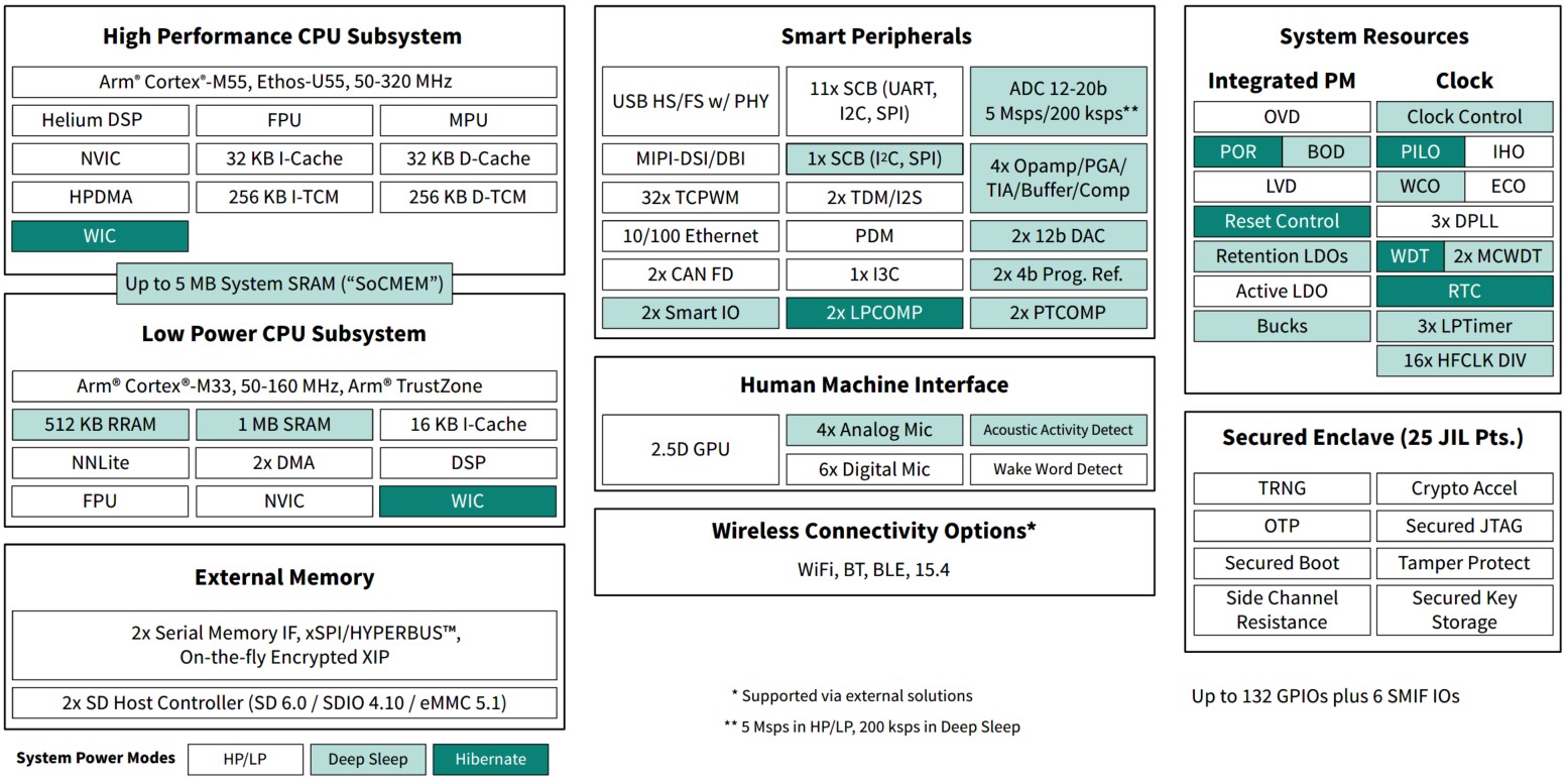
The PSOC™ Edge E84 EVK is built around a PSOC™ Edge E84.
Figure 4
shows the Architecture block diagram of the PSOC™ Edge E84 MCU used on the board. For details of device features, see the
datasheet
.
Figure 4.
PSOC™ Edge E84 MCU block diagram
Figure 5.
PSOC™ Edge E84 Evaluation Board top-level block diagram
Figure 6.
Baseboard top view with SOM connected
Figure 7.
Baseboard bottom view
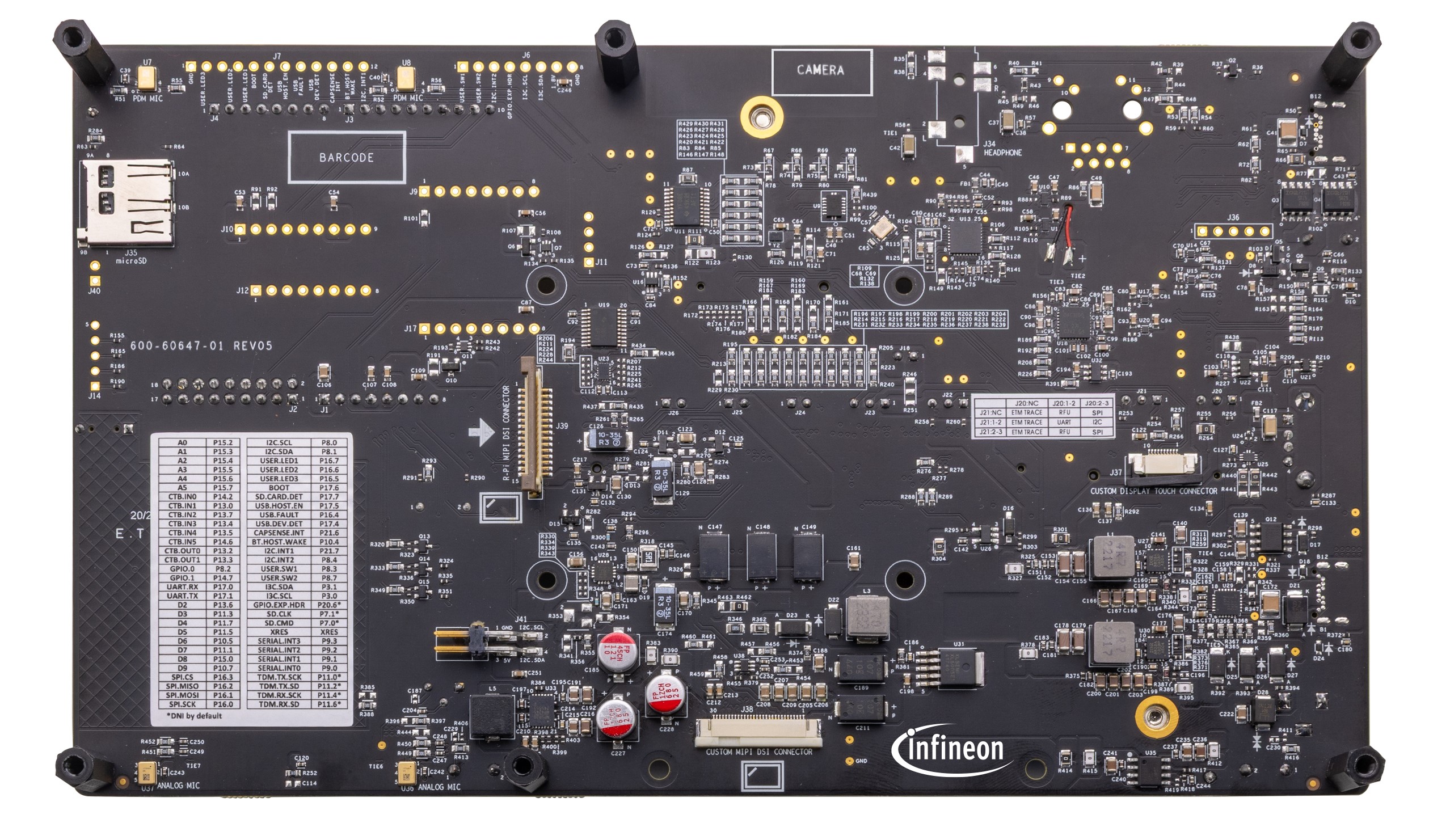
Figure 8.
PSOC™ Edge E84 SOM (top view)
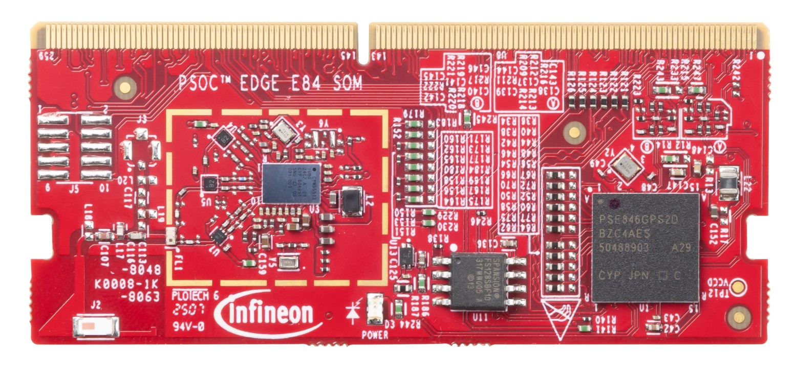
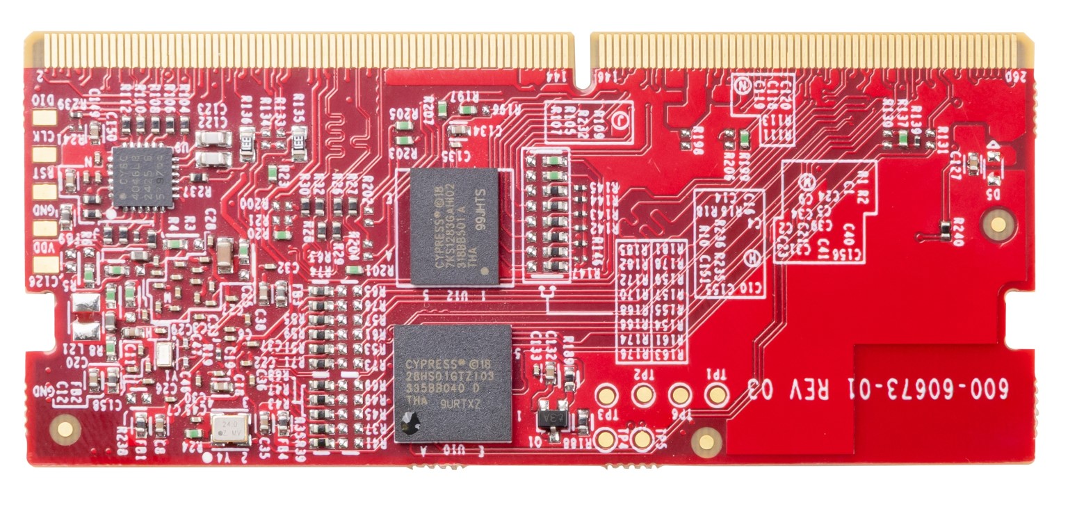
Figure 9.
PSOC™ Edge E84 SOM (bottom view)
lists the kit peripherals.
SI. No. | Peripheral | Description |
|---|---|---|
Power LED (D1) | Amber LED that indicates the status of the power supplied to board. | |
KitProg3 Program/Debug USB Type-C connector (J8) | Use the USB cable provided along with the EVK to connect the board to a PC to power(5 V, maximum 3 A) the board and program/debug using the KitProg3 onboard programmer and debugger. | |
PSOC™ 5LP based KitProg3 programmer and debugger (CY8C5868LTI-LP039, U2) | The PSOC™ 5LP MCU (CY8C5868LTI-LP039) serving as KitProg3, is a multifunctional system, which includes a SWD programmer, debugger, USB-I2C bridge and USB-UART bridge. KitProg3 also supports custom applications. For more details, see the KitProg3 User Guide . | |
Reset button (SW1) | This button resets the PSOC™ Edge E84 MCU. It connects the PSOC™ Edge E84 MCU reset (XRES) pin to the ground when pressed. | |
KitProg3 status LED (D2) | Amber LED (D2) indicates the status of KitProg3. For details on the KitProg3 status, see the KitProg3 User Guide . By default, this LED should be ON which indicates CMSIS-DAP/Bulk mode. | |
PSOC™ Edge E84 MCU ETM/JTAG debug and trace header (J15) | This 20-pin header provision allows for JTAG debug and ETM trace for instruction/data tracing in PSOC™ Edge E84 MCU. | |
PSOC™ Edge E84 MCU program and debug interface header (J16) | This 10-pin standard SWD/JTAG header provision allows to interface external programmers such as MiniProg4 for programming and debugging. | |
Alternative serial interface configuration headers (J20, J21) | Configuration headers for ETM trace data line 2 and trace data line 3. These lines are used to configure alternate serial interfaces like I2C, UART, SPI | |
PSOC™ Edge E84 MCU USB Host Type-A connector (J27) | A USB Type-A cable can be connected between this USB connector and the PC to use the PSOC™ Edge E84 MCU USB Host applications. | |
USB Type-C PD connector Fault LED (D6) | USB Type-C Fault detect LED | |
11 | Custom display Capacitive Touch Panel connector (J37) | Touch connector for custom display for HMI (Human Machine Interface) applications, such as wearables. |
12 | PSOC™ Edge E84 MCU USB device Type-C connector (J30) | Use this USB connector to connect to a PC for using the PSOC™ Edge E84 MCU USB device applications. This connector can be used to power the kit at higher voltage and current, it supports PD at 15 V, maximum 3 A or 5 V, maximum 3 A |
13 | External power supply VIN connector (J31) | Connects an external DC power supply input to the on-board regulators. Input Range is 7 V to 12 V for this VIN supply. |
14 | PSOC™ Edge E84 MCU user buttons (SW2, SW4) | Provides an input to PSOC™ Edge E84 MCU. Note that the button connects the PSOC™ Edge E84 MCU pin to ground when pressed by default. Therefore, configure the MCU pin as a digital input with resistive pull-up for detecting the button press. These buttons also provide a wake-up source from low-power modes of the device. |
M.2 (B-key) memory interface connector (J29) | M.2 B-Key socket to interface M.2 compatible external flash and PSRAM interfaces to PSOC™ Edge E84 MCU. | |
Processor SoM 260-pin SODIMM connector (J28) | SODIMM connector header for connecting MCU SoM module | |
128-Mbit Octal-SPI HYPERRAM™ (U12) | 128 Mb HYPERRAM™ device is a high-speed CMOS, self-refresh DRAM, The HYPERRAM™ device provides an xSPI (Octal) slave interface to the host system. The xSPI (Octal) interface has an 8-bit (1 byte) wide DDR data bus and use only word-wide (16-bit data) address boundaries. | |
CYW55513 Tri-band (Wi-Fi/Bluetooth®) Combo Radio (U3) | Onboard AIROC™ Wi-Fi and Bluetooth® combo for connectivity applications, supports Bluetooth® 5.4 and Wi-Fi 6/6E | |
R-Pi compatible MIPI-DSI display connector (J39) | Connector header for R-Pi compatible displays. | |
1-Gbit Octal-SPI NOR Flash (U10) | 1-Gbit high-speed CMOS, MIRRORBIT™ NOR flash devices support both the octal peripheral interface (OPI) as well as legacy connection signals. | |
MIPI-DSI custom display connector (J38) | Generic connector header for MIPI-DSI compatible displays for HMI (Human Machine Interface) applications, such as wearables. | |
128-Mbit Quad-SPI NOR Flash (U11) | 128-Mbit non-volatile memory, connects to a host system via a SPI interface. The memory is ideal for code shadowing to RAM, executing code directly, execute code in place (XIP), and storing reprogrammable data. | |
PSOC™ Edge E84 MCU (220-BGA, U1) | This kit is designed to highlight the features of the PSOC™ E84 MCU. For details on PSOC™ E84 MCU pin mapping, refer to Table 2 | |
PSOC™ 4000T CAPSENSE™ Coprocessor (U9) | PSOC™ 4000T as onboard Co-processor for CAPSENSE™ feature enablement, connected to MCU via I2C interface | |
6-axis Accelerometer and Gyroscope IMU (U5) | BMI270 is a 6-axis IMU with Accelerometer and Gyroscope combination which is interfaced to PSOC™ Edge E84 MCU over I2C serial interface. | |
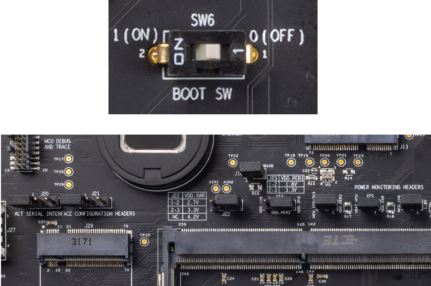
PSOC™ Edge E84 MCU Boot Select (SW6) | Based on this switch's configuration the MCU can boot from one of the following boot sources - External FLASH or Internal RRAM. | |
Linear Potentiometer (R34) | 10 KΩ potentiometer connected to PSOC™ Edge E84 MCU pin P15[1]. It can be used to simulate an analog sensor output to PSOC™ Edge E84 MCU. | |
Analog microphones (U36, U37) | Onboard analog microphones for Voice User Interface (VUI) applications like smart speakers, home automation and IoT devices. | |
User LEDs (D3, D4, D5) | Can be controlled by the PSOC™ Edge E84 MCU. The LEDs are active HIGH, so the pins must be driven to logic level 1 to turn ON the LEDs. | |
Thermistor (TH1) | This thermistor can be used for temperature compensation or as a general purpose ambient temperature sensor (MCU pin is not connected to thermistor by default. See rework section for more details) | |
CAPSENSE™ buttons and slider (CSB1, CSB2, CSS1) | The CAPSENSE™ touch-sensing slider and two buttons, all of which are capable of both self-capacitance (CSD) and mutual-capacitance (CSX) operation, allow you to evaluate Infineon’s fourth-generation CAPSENSE™ technology. The slider and buttons have a 1 mm acrylic overlay for smooth touch sensing. | |
Proximity sense connector (J19) | Connector for capacitive proximity sense. | |
Arduino UNO R3 compatible I/O headers (J2, J3, J4) | Brings out pins from PSOC™ Edge E84 MCU to interface with shields compatible with Arduino. Some of these pins are multiplexed with on-board peripherals. For a detailed information on how to rework the kit to access other functions, see Table 2 . | |
Arduino UNO R3 compatible power header (J1) | Powers the shields compatible with Arduino. It also has a provision to power the kit though the VIN input. | |
Alternative serial interface I/O header (J14) | Header for alternate serial interface I/Os | |
microSD card holder (J35) | Provides SDHC interface with microSD cards with the option to detect the presence of the card. | |
Infineon’s Shield2Go interface headers (J10, J12) | The Header provides an easy plug and play interfacing of Infineon's Shield2Go boards. Some pins of this connector is not connected to MCU by default. Check the rework section for more details. | |
PDM microphones (U7, U8, Bottom) | Two microphones convert voice inputs to Pulse-Density Modulated (PDM) digital signals. | |
PSOC™ Edge E84 MCU expansion I/O headers (J6, J7, J40) | Provide connectivity to PSOC™ Edge E84 MCU GPI/Os. Some of these I/Os are also connected to on-board peripherals. See Table 2 for pin mapping. This is not loaded by default. | |
mikroBUS compatible headers by MikroElektronika (J9, J17) | Interfaces add-on boards compatible with mikroBUS by MikroElektronika. Some pins of this connector is not connected to MCU by default. Check the rework section for more details. | |
Extended I2S header (J11) | Provides I2S(TDM) output signals. This connector is not populated by default on the kit | |
3-axis Magnetometer (U4) | BMM350 is a 3-axis Magnetometer which is interfaced to PSOC™ Edge E84 MCU over I3C serial interface. | |
M.2 (E-key) radio interface connector (J29) | M.2 (E-key) radio interface connector (J29): M.2 E-Key socket to interface compatible AIROC™ Wi-Fi & Bluetooth® combo M.2 radio modules. | |
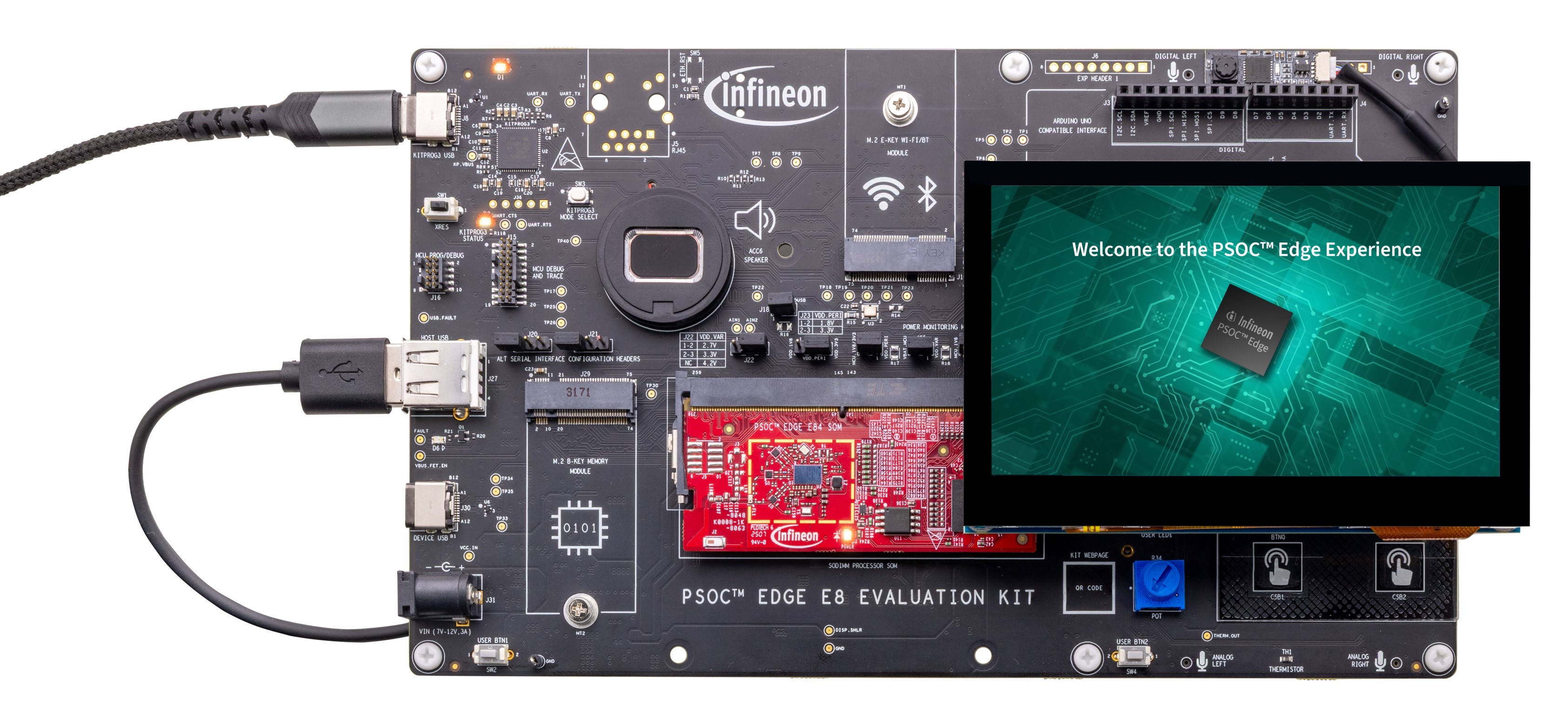
PSOC™ Edge E84 MCU power selection/monitoring headers (J18, J22, J23, J24, J25, J26) | Headers for configuring power domains like MCU and peripheral power domain. Also, this hardware section has power measurement jumpers, connect an ammeter to these jumpers to measure current in the respective power domains. | |
Headphone connector (J34) | Headphone Jack Stereo connector. This connector is not populated by default on the kit | |
Speaker (ACC6) | On-board 8Ω speaker with 8W output. | |
RJ45 Ethernet MagJack connector (J5) | RJ45 Ethernet connector port to connect the kit to an ethernet network. This connector is not populated by default on the kit | |
KitProg3 programming mode selection button (SW3) | This button can be used to switch between various modes of operation of KitProg3 (CMSIS-DAP/Bulk or CMSIS-DAP/HID mode). For more details, see the KitProg3 User Guide . By default, the programming mode is set to CMSIS-DAP/Bulk which allows faster programming than CMSIS-DAP/HID. |
See
Hardware functional description
for details on various hardware blocks.
Using the OOB example
The PSOC™ Edge E84 evaluation kit is by default programmed with the code example: PSOC™ E84 MCU: PSOC™ E84 OOB demo app. The following steps describe on how to use the example. For a detailed description of the project refer to the example’s
README.md
file in the GitHub repository. The
README.md
file is also in the application directory once the application is created.
Note:
At any point of time, if you overwrite the OOB example, you can restore it by programming the PSOC™ E84 MCU: PSOC™ E84 OOB demo app.
Before you start ensure that you have the following:
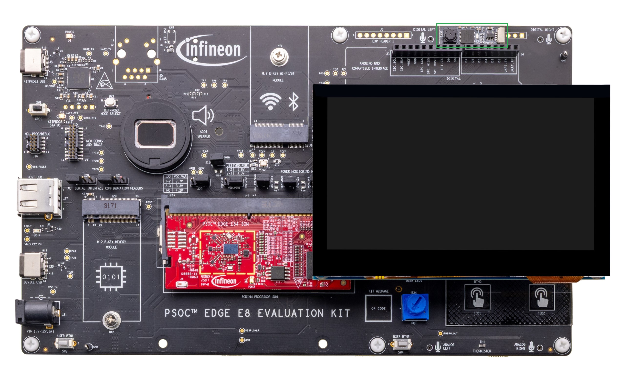
PC with USB Type-C port. (In case USB Type C port is absent in PC use a USB Type-A to USB Type-C connector cable which is not provided with EVK)
Attach camera module to preferred location (Image shows the recommended location on baseboard)
Before attaching the camera, ensure the PCB surface is clean and free of debris. If necessary, use a soft cloth and a cleaning solution to gently wipe the surface
Gently peel the cover away from the 3M tape
Carefully align the camera module with the preferred mounting area on the baseboard
Once the camera is aligned, gently press it onto the baseboard
Remove protective film from Camera lens
Connect the 4 pin connector of camera's USB cable to camera module
Figure 10.
Camera Module placement
Connect and power up the board
Ensure that the Boot configuration switch (SW6) is in OFF position
Ensure that jumpers are set to their default positions as below:
J22, J23: 2-3
J18, J24, J25, J26: SHORT
J20, J21: OPEN
Connect the camera module cable to USB host Type-A connector on baseboard(J27)
Connect the KitProg3 USB connector (J8) to your PC using the Type-C to Type-C USB cable
Ensure that the power LED (D1, yellow) on the base board is ON
Ensure that the power LED (D3, yellow) on the System on Module (SOM) board is ON
Figure 11.
Boot switch and jumper configuration
Run the pre-programmed code examples
Observe the splash screen boot-up on the 4.3 inch display
A carousal menu appears listing the demo applications pre-programmed into the kit
Select the application to be demonstrated
Follow the instructions (if any) presented by the demo app
Press the
Home
button to get back to main menu
Press the XRES button (SW1) to reboot the device to splash screen (if required)
Visit the
PSOC™ Edge E84 Evaluation Kit
webpage for latest software and other kit documentation
Figure 12.
PSOC™ Edge E84 Evaluation Kit
OOB Demo
Creating a project and program/debug using ModusToolbox™ software
The PSOC™ Edge E84 evaluation kit can be programmed and debugged using the on-board KitProg3. KitProg3 is an on-board programmer/debugger with USB-UART, USB-I2C Bridge functionality. KitProg3 supports CMSIS-DAP only and does not support mass storage. A PSOC™ 5LP device is used to implement the KitProg3 functionality. For more details on the KitProg3 functionality, see the
KitProg3 user guide
.
This following steps briefly introduces project creation, programming, and debugging using ModusToolbox™ software. For detailed instructions, see
Help >
Eclipse for ModusToolbox™
Documentation > User Guide
Connect the board to the PC using the provided USB cable through the KitProg3 USB connector, as shown in
Figure 13
. It enumerates as a USB Composite Device if you are connecting it to your PC for the first time
KitProg3 on this kit supports CMSIS-DAP Bulk mode (default) and CMSIS-DAP Bulk with two UARTs. The status LED (amber) is always ON in the CMSIS-DAP Bulk mode. If you do not see the desired LED status, see the
KitProg3 user guide
for details on the KitProg3 status and troubleshooting instructions
Note:
The programming can be done in either of the KitProg3 programming modes but it is recommended to program the kit in CMSIS-DAP Bulk mode.
Figure 13.
Connect USB cable to USB connector on the board
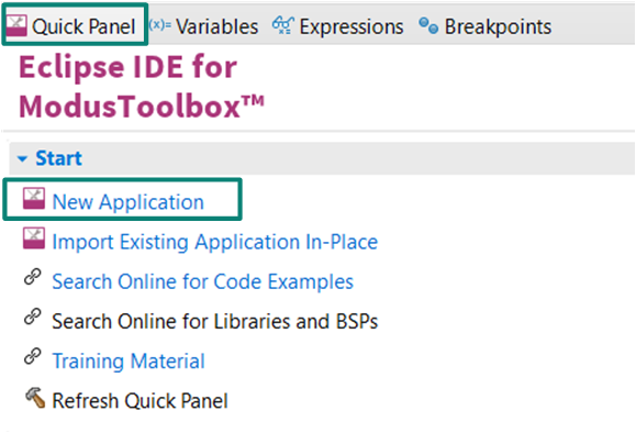
In the Eclipse IDE for ModusToolbox™ software, import the desired code example (application) into a new workspace
Click on
New Application
from
Quick Panel
Figure 14.
Create new application
Select the BSP -
KIT_PSE84_EVAL
in the “Choose Board Support Package” window and click
Next
Figure 15.
Creating a new application: Choose Board Support Package
Select the application from
Select Application
window and click
Create
Figure 16.
Creating a new application: Select Application
To build and program a PSOC™ E84 MCU application, in the Project Creator, select ui
project. In the Quick Panel, scroll to the Launches section and click the
<App_Name> Program (KitProg3_MiniProg4)
configuration as shown in
Figure 17
Figure 17.
Programming in ModusToolbox™ software
ModusToolbox™ software has an integrated debugger. To debug a PSOC™ E84 MCU application, in the Project Creator, select
project. In the Quick Panel, scroll to
Launches
section and click the
<App_Name> Debug (KitProg3_MiniProg4)
configuration as shown in
Figure 18
. For more details, see the “Program and debug” section in the
Eclipse IDE for ModusToolbox™ user guide
Figure 18.
Debugging in ModusToolbox™ software
Hardware
Schematics
Hardware functional description
MOD_PSE84_SOM
PSOC™ Edge E84 MCU
PSOC™ Edge E84 MCU has the following features:
High-performance compute, graphics, audio, DSP, and machine learning (ML) blocks
Low-power CPU block for security, control, and communication
Low-power operation: Multiple power modes; DC-DC buck converter; dynamic voltage and frequency management
Optimizable power: independent voltage domains; selectable SRAM retention
Communications and connectivity: USB, SD host, Serial Memory Interface (SMIF), Ethernet, CAN FD, I3C, I2C, UART, SPI
Always-on power domain: Autonomous Analog with ADC, DAC, opamps, comparators, Acoustic Activity Detection (AAD)
Programmable GPIO pins: drive modes, strengths, and slew rates; over-voltage tolerant (OVT) pins for I2C compliance. Some ports have a smart I/O programmable logic array
Potential applications are:
Smart home appliance
Smart thermostat
Industrial HMI
This product line is a dual-CPU microcontroller with a neural net companion processor, DSP capability, high-performance memory expansion capability, low-power analog subsystem with high-performance analog-to-digital conversion and low-power comparators, IoT connectivity, communication channels, and programmable analog and digital blocks. It also has audio and graphics blocks.
In a multi-domain architecture, PSOC™ Edge E84 MCU supports the security, communications and control, and DSP. This enables the fine-grained power optimization and dynamic frequency and voltage scaling. The always‑on domain supports voice recognition, wake-on-touch, battery monitoring, and other sensing applications. These functions are provided at extremely low power.
Figure 19.
MCU block diagram
PSOC™ Edge E84 MCU power supply system
This product line operates with a single 1.8 V ±5% regulated supply, or from a 2.7 V to 4.8 V VBAT supply along with a 1.8 V 5% regulated supply.
The core logic can operate at different levels with a trade-off in performance and power. In addition with clock gating at peripheral and bus levels, this permits fine-grained optimization of energy usage. A buck regulator powers the core logic at three levels: 0.7 V, 0.8 V, and 0.9 V. The buck efficiency is ≥80% in the active power mode. The buck configuration is single in, single out (SISO).
System-on-Module (SoM) provides the following two modes of powering the MCU:
Power on with VBAT(3.3 V) by default
1.8 V regulated supply with rework
All MCU IOs can operate at 1.8 V logic level only. P16 and P17 can be operated at 1.8 V or 3.3 V by changing the jumper setting on the baseboard.
By default, USB IP is powered by the 3.3 V supply voltage that is connected via a jumper (for power measurement) on the baseboard.
Ferrite bead FB1-FB4 is included to reduce the switching noise between the digital and analog power supplies within the domain.
Figure 20.
PSOC™ Edge E84 power supply system (1)
Figure 21.
PSOC™ Edge E84 power supply system (2)
PSOC™ Edge E84 MCU I/Os
PSOC™ Edge E84 SOM will bring out all the High speed and Low speed IOs to the baseboard through 260-pin Edge connector, some are directly connected to on-board peripherals and some are routed and exposed on header.
ECO , WCO and EXT clock and SWD pins are dedicated in the board. Few IOs are multiplexed in the SOM for the alternate functionality. See
PSOC™ Edge E84 kit rework
section for using alternate functions.
Figure 22.
MCU GPIO
HSIO (SMIF0, SMIF1, MIPI DSI, and USB) pins along with the clock and SWD are dedicated from the MCU and connected directly to the peripherals.
Figure 23.
MCU HSIO
Clock architecture for PSOC™ Edge E84
PSOC™ Edge E84 SOM board includes 32.768 KHz WCO(
Y1
) and 17.2032 MHz ECO ( Y2 ) for the PSOC™ Edge E84 MCU device and 24 MHz ( Y4 ) oscillator input as external clock input for the USB functionality..
There will be a dedicated 24 MHz clock input for enabling the USB interface as host and device from the MCU. Dedicated External Crystal Oscillator 17.2032 MHz for the internal PLL block and WCO 32.768 KHz for the RTC block.
Figure 24.
PSOC™ Edge E84 clock sources
PSOC™ Edge E84 programming header
PSOC™Edge E84 MCU can be programmed alternatively through a 10-pin SWD ( J5 ) using Miniprog4.
By default, to program the PSOC™Edge E84 MCU, plug the SOM on the baseboard as J5 is not mounted on the SOM.
Figure 25.
MCU programming header
Memory subsystem
Quad-SPI flash
PSOC™ Edge E84 SOM board has an Infineon Quad SPI NOR flash memory (U11) of 128 Mb capacity (S25FS128SAGMFB100).
The NOR flash is connected to the Quad SPI interface of the PSOC™ Edge E84 MCU device. The NOR flash device supports 4-bit (Quad I/O) serial commands. By default, Smif0_Select1 is connected to this interface. IO lines are shared between the Octal and Quad flash in this board. In the Quad DDR mode, the device operates at 80 MBps with the 80 MHz clock. In the Quad SDR mode, it operates at 66 MBps with the 133 MHz clock.
Octal flash
PSOC™ Edge E84 SOM board has an Infineon SEMPER™ Octal flash memory (S28HS01GTGZBHI030) (U10) of 1 Gb capacity.
The NOR flash is connected to the Octal xSPI interface of the PSOC™ Edge E84 MCU device. The NOR flash device supports 8-bit (Octal I/O) serial commands. The device can operate up to 200 MBps in SDR mode and 400 MBps in DDR mode.
Figure 26.
Quad and Octal SPI flash
HYPERRAM™
PSOC™ Edge E84 SOM board has an Infineon HYPERRAM™ memory (S70KS1283GABHI020) (U12) of 128 Mb capacity.
The PSRAM is connected to the Octal xSPI interface of the PSOC™ Edge E84 MCU device. The PSRAM device supports 8-bit (Octal I/O) serial commands. The device can operate only in DDR mode with 400 MBps data rate.
Figure 27.
HYPERRAM™
AIROC™ CYW55513 Wi-Fi & Bluetooth® radio
AIROC™ CYW55513 Wi-Fi & Bluetooth® is an low-power, single chip device that support single-stream, tri-band, Wi-Fi 6/6E, IEEE 802.11ax compliant Wi-Fi MAC/baseband/radio, and Bluetooth®/Bluetooth® Low Energy 5.4.
PSOC™ Edge E84 device communicates to this device using a standard SDIO interface for WLAN and BT_UART for Bluetooth® operation along with the handshake signals. AIROC™ CYW55513 Wi-Fi & Bluetooth® radio supports the following:
BT_Reg_ON controls the regulator power of the Bluetooth® host
WL_Reg_ON controls the regulator power of the WLAN host
Bluetooth® host wake and WL host wake are connected to invoke the IC during the power down mode
Bluetooth® device wake and WL device wake to invoke the radio from host
Bluetooth® communication can happen with the 115200 maximum baud rate
WLAN can communicate over an SDIO interface at SDR50 or DDR50 speed
Radio PMU topology
AIROC™ CYW55513 powers on with an external VBAT supply that is 3.3 V and the IO supply voltage 1.8 V from the baseboard. All the additional power for RF switches, power amplifiers will be derived from the internal regulators.
Figure 28.
AIROC™ CYW55513 - power1
Figure 29.
AIROC™ CYW55513 - power 2
Power LED
LED D3 glows when the SOM board is powered and this will ensure that the radio and peripheral supplies are in nominal voltage.
Load switch for AIROC™ CYW55513 power sequence
U13 ensures that the AIROC™ CYW55513 IC will be powered once the VBAT_Radio supply comes first and then IO supply H1_1V8, which will satisfy the power sequence requirement of the IC.
Figure 30.
Load switch and Power LED
Radio subsystem
AIROC™ CYW55513 communicates with the host MCU through the SDIO and UART interface.
Figure 31.
Radio subsystem
Clock architecture for radio
PSOC™ Edge E84 SOM board includes 37.4 MHz ECO (
Y3
), 32.768 KHz WCO (
Y5
) for the AIROC™ CYW55513 device.
There is an option to use the LPO (
Y6
) oscillator input for the 32.768 KHz that is DNI by default.
Figure 32.
AIROC™ CYW55513 clock sources
RF matching network
PSOC™ Edge E84 SOM board includes a Pi-type matching network for the 2 GHz and 5 GHz paths of WLAN and Bluetooth®, which is connected before and after the RF switches to control the impedance to 50 Ω.
Figure 33.
RF matching network
RF front end
PSOC™ Edge E84 SOM board includes RF switches, diplexer, onboard chip antenna (default) and option to test with external antenna using UFL connectors.
Figure 34.
RF front end
CAPSENSE™ coprocessor
The PSOC™ Edge E84 SOM board has onboard PSOC™ 4000T ( U9 ), which is used as a CAPSENSE™ coprocessor. This senses the data from the slider, buttons and the proximity sensor in mutual cap mode and will communicate to the host via an I2C interface with the default slave ID "0x0C".
You can program the CAPSENSE™ IC using the bootloader code, which will dump the program from the host MCU to CAPSENSE™ using I2C.
Figure 35.
PSOC™ 4000T device
AMIC signal processing circuit
Circuit is used to tune the frequency response and the signal amplitude of AMIC, which is present on the baseboard.
Figure 36.
RC compensation circuit
PSOC™ Edge E8 Base Board
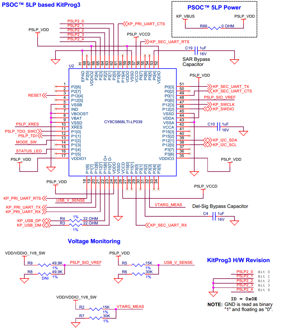
PSOC™ 5LP as onboard programmer/debugger
PSOC™ 5LP-based KitProg3
PSOC™ 5LP-based KitProg3 to program and debug the PSOC™ Edge E84 MCU.
An onboard PSOC™ 5LP (CY8C5868LTI-LP039,
U2
) device is used as KitProg3 to program and debug the PSOC™ Edge E84 MCU. The PSOC™ 5LP device connects to the USB port of a PC through a USB connector and to the SWD/JTAG and other communication interfaces of the PSOC™ Edge E84 MCU. KitProg3 uses 5 pins for hardware ID definition. These I/Os can be either connected to the ground (active state) or left floating. The KitProg3 firmware reads the state of these pins with software inversion and get the specific hardware ID value which describes the unique Kit features set. Also, it features voltage monitor pins which sense the USB bus voltage, target device supply and Smart IO reference voltage which For more information, see the
PSOC™ 5LP
webpage and
Kitprog3 User Guide
Figure 37.
Schematic of PSOC™ 5LP-based KitProg3
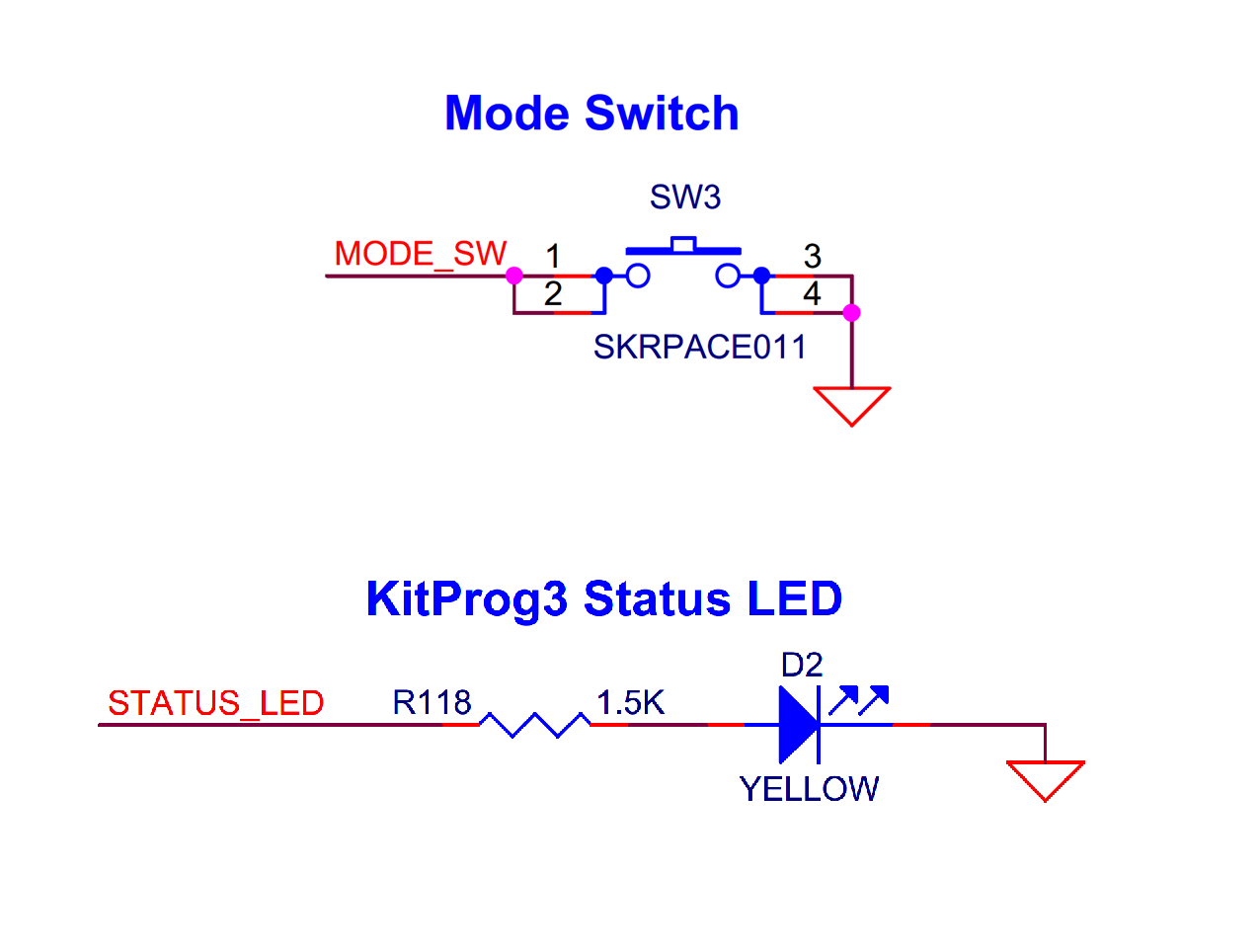
KitProg3 programming mode selection button and status LED
There is a mode selection button (
SW3
) connected to the PSOC™ 5LP device for programming mode selection. This button can be used to switch between modes (see the
Kitprog3 user guide
for details). The button works in active LOW configuration and shorted to GND when pressed.
PSOC™ 5LP has a status LED (
D2,
yellow) which indicates the programming status. See
Table 5
for a summary of the status LED states.
KitProg3 programming modes | Status LED (D2) |
|---|---|
CMSIS-DAP/Bulk mode (default) | ON |
CMSIS-DAP/HID mode | RAMPING at 1 Hz |
Figure 38.
Schematic of KitProg3 mode switch and status LED
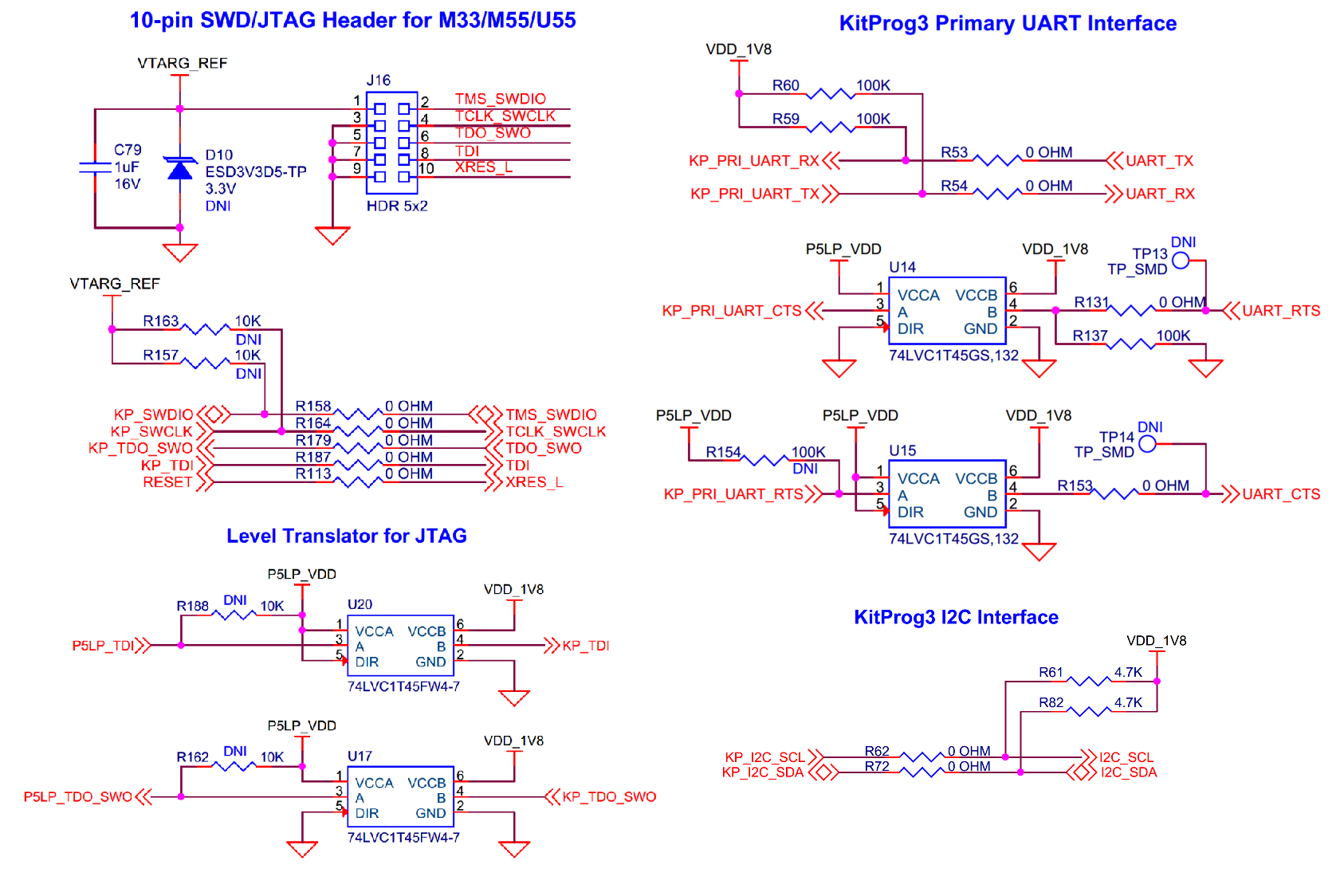
Serial interconnection between PSOC™ 5LP and PSOC™ Edge E84
In addition of use as an on board programmer/debugger using SWD/JTAG interface, the PSOC™ 5LP device also functions as an interface for the USB-UART and USB-I2C bridges, as shown in
Figure 39
. The USB-Serial pins of the PSOC™ 5LP device are hard-wired to the I2C/UART pins of the PSOC™ Edge E84 MCU. The Primary UART interface supports hardware flow control. The I2C pins are also available on the Arduino compatible I/O header, mikroBUS Click header and IFX Shield2Go header; therefore, the PSOC™ 5LP device can be used to control Arduino, mikroBUS Click and Infineon's Shield2Go shields with an I2C interface.
PSOC™ 5LP signal | PSOC™ Edge E84 I/O (signal) | Logic Level |
|---|---|---|
KP_SWCLK | P6[3] (TCLK_SWCLK) | 1.8 V |
KP_SDWIO | P6[2] (TMS_SWDIO) | 1.8 V |
KP_TDO_SWO | P6[0] (TDO_SWO) | 5 V (P5LP), 1.8 V (PSOC™ Edge E84) |
KP_TDI | P6[1] (TDI) | 5 V (P5LP), 1.8 V (PSOC™ Edge E84) |
RESET | XRES (XRES_L) | 1.8 V |
KP_I2C_SCL | P8[0] (I2C_SCL) | 1.8 V |
KP_I2C_SDA | P8[1] (I2C_SDA) | 1.8 V |
KP_PRI_UART_TX | P6[5] (UART_RX) | 1.8 V |
KP_PRI_UART_RX | P6[7] (UART_TX) | 1.8 V |
KP_PRI_UART_RTS | P6[4] (UART_CTS) | 5 V (P5LP), 1.8 V (PSOC™ Edge E84) |
KP_PRI_UART_CTS | P6[6] (UART_RTS) | 5 V (P5LP), 1.8 V (PSOC™ Edge E84) |
Figure 39.
Schematic of Serial Interconnection between PSOC™ 5LP and PSOC™ Edge E84
Serial interconnection between PSOC™ 5LP and radio interface
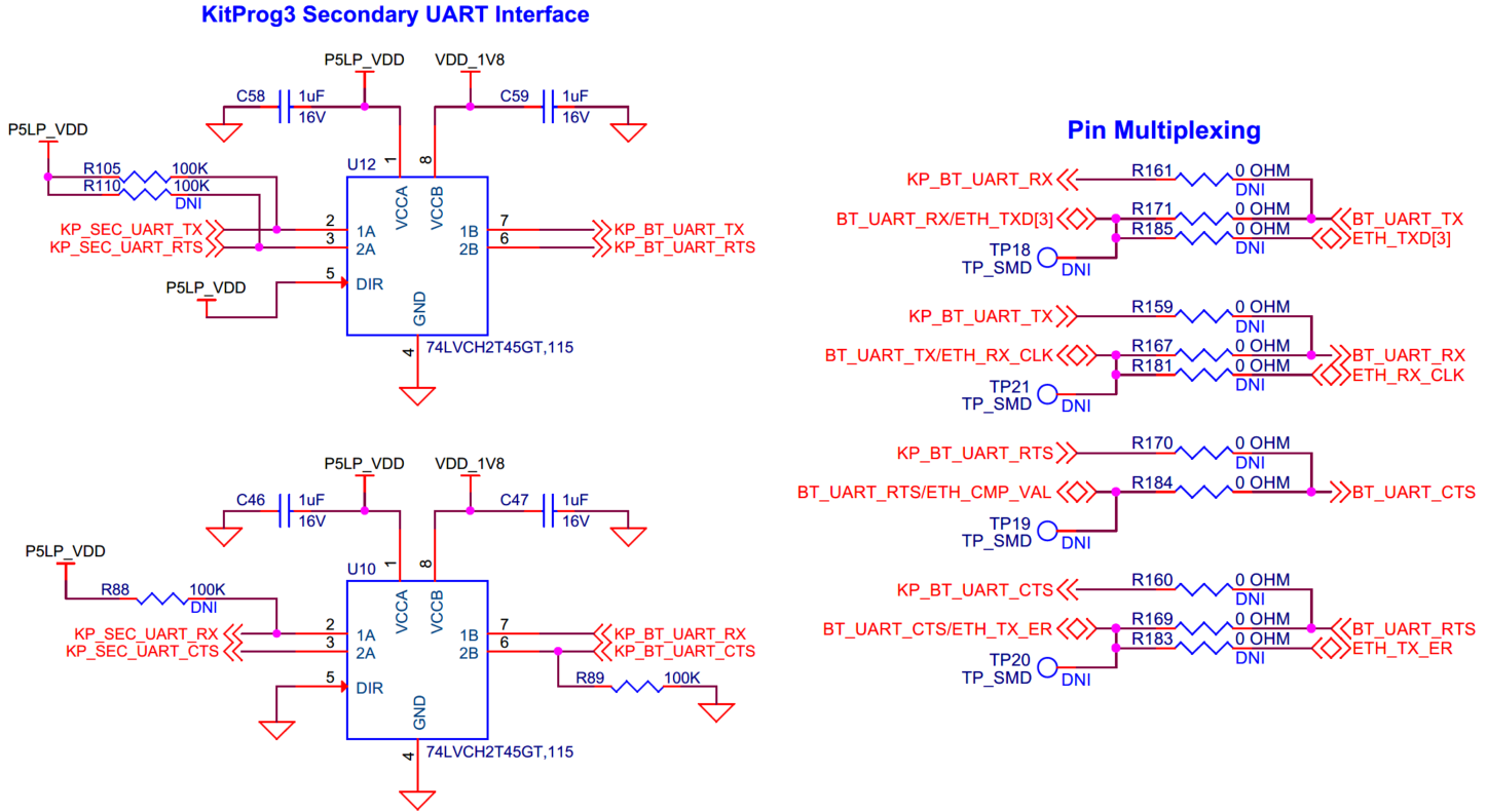
Serial interconnection between PSOC™ 5LP and onboard AIROC™ CYW55513/M.2 radio interface.
The PSOC™ 5LP device also has a secondary UART interface that can be connected to BT_UART of the on board AIROC™CYW55513 or the M.2 Radio interface connector (
J13
). Note that, it is connected to the AIROC™ CYW55513 device on SOM by default. To change it to M.2 radio, see the section
Rework for M.2 external radio interface
. The secondary UART interface supports hardware flow control.
Figure 40.
Schematic of serial interconnection between PSOC™ 5LP and radio interface
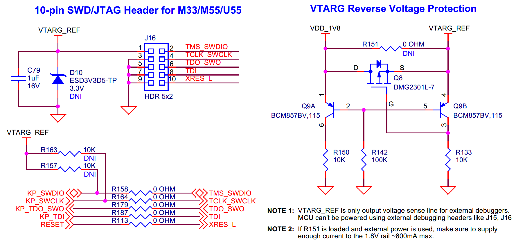
PSOC™ Edge E84 MCU external program/debug headers
10-pin SWD/JTAG header
10-pin SWD/JTAG interface for programming or debugging PSOC™ Edge E84 MCU.
PSOC™ Edge E84 MCU can be programmed/debugged alternatively through a 10-pin SWD/JTAG header (
J16
) using a MiniProg4 programmer or any third-party programmer.
Also, there is a reverse voltage protection circuit provided on the VTARG_REF power rail which means the PSOC™ Edge E84 or any other on board peripheral can not be powered from the 10-pin SWD/JTAG header (
J16
) or 20-pin ETM/JTAG header (
J15
). This is to protect the external programmer from overloading, making sure that the kit doesn’t draw any current from the external programmer through
J16
or
J15
.
Do note that the JTAG interface will not work by default through
J16
. See section
Rework for JTAG interface using external programmer/debugger
to enable the JTAG support.
Signal name | PSOC™ Edge E84 I/O | Logic level |
|---|---|---|
TCLK_SWCLK | P6[3] | 1.8 V |
TMS_SWDIO | P6[2] | 1.8 V |
TDO_SWO | P6[0] | 1.8 V |
TDI | P6[1] | 1.8 V |
XRES_L | XRES | 1.8 V |
Figure 41.
Schematic of 10-pin SWD/JTAG program/debug header
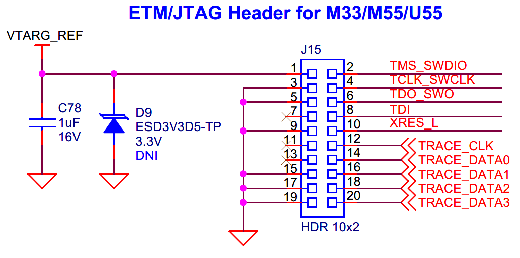
20-pin ETM/JTAG header
20-pin ETM/JTAG interface for programming or debugging PSOC™ Edge E84 MCU.
PSOC™ Edge E84 MCU can also be programmed/debugged through a 20-pin ETM TRACE or JTAG header (
J15
) using any third-party programmer.
Do note that the JTAG interface will not work by default through
J15
. See section
Rework for JTAG interface using external programmer/debugger
to enable the JTAG support. Also note that, pins TRACE_DATA2 and TRACE_DATA3 are available on J21 and J20 respectively for alternate serial interface configuration.
Signal name | PSOC™ Edge E84 I/O | Logic level |
|---|---|---|
TCLK_SWCLK | P6[3] | 1.8 V |
TMS_SWDIO | P6[2] | 1.8 V |
TDO_SWO | P6[0] | 1.8 V |
TDI | P6[1] | 1.8 V |
XRES_L | XRES | 1.8 V |
TRACE_CLK | P20[0] | 1.8 V |
TRACE_DATA0 | P20[4] | 1.8 V |
TRACE_DATA1 | P20[3] | 1.8 V |
TRACE_DATA2 | P20[2] | 1.8 V |
TRACE_DATA3 | P20[1] | 1.8 V |
Figure 42.
Schematic of 20-pin ETM/JTAG program/debug header
Power supply system
Power inputs and over-voltage protection
Power supply options for the kit and over-voltage protection circuit.
The power supply system on this board is versatile, allowing the board to be supplied from any of the following sources:
5 V/3A from the on board KitProg3 Type-C USB connector ( J8 )
5 V-15 V/3A from the Device Type-C USB connector ( J30 )
7 V-12 V/3A power from VIN header ( J31 ) or 7 V-12 V from Arduino header ( J1.1 )
The power supply system is designed to provide 1.8 V (core and I/O), 3.3 V (I/O), 2.7 V-4.2 V (VBAT) operating voltages to the PSOC™ Edge E84 MCU and 5 V for the PSOC™ 5LP based KitProg3 operation. Apart from that, 1.8 V, 3.3 V, and 5 V rails are also used to power the different on board peripherals.
The KitProg3 Type-C USB connector ( J8 ) can provide 5 V/3A and the host must have the power rating capability of 5 V/3 A. The power rail KP_VBUS_IN is connected to a 5 V over voltage protection (OVP) circuit which protects the on board PSOC™ 5LP and other components from over voltage. This OVP circuit has a cut-off range from 5.25 V (min) to 6.5 V (max) based on the component tolerance. Therefore, the maximum recommended voltage through
J8
is 5.25 V. Note that PSOC™ 5LP will only get power when powered from J8 .
On the other hand, Device Type-C USB connector (
J30
) is configured to provide 5 V-15 V/3 A power using on board BCR controller (
U29
). Refer to section
Device Type-C USB EZ-PD™ BCR controller
for more details.
The supply rails KP_VBUS (5 V from header
J8
through OVP), VBUS_DEV_OUT (5 V-15 V from header
J30
through 3 A load switch) and VIN (7 V-12 V from header
J31
or
J1.1)
are combined into VCC_IN through ‘OR’ing diodes (
D25
-
D27
) as shown in the figure below.
Note that, it is recommended to power the board with minimum 9 V through Device Type-C USB connector (
J30
) or 7 V through VIN header (
J31
) when powering the MCU with VBAT = 4.2 V.
Also, it is highly recommended to power the board from the Device Type-C USB connector (
J30
) or VIN header (
J31
) with minimum 9 V/3 A when using any power-hungry peripherals like large display.
Figure 43.
Block diagram of power architecture
Figure 44.
Schematic of power inputs and over-voltage protection
Voltage regulators
On board voltage regulators for power delivery.
There are four voltage regulators on the board:
1.8 V LDO ( U35 ): Powers the PSOC™ Edge E84 (core and I/O domains) and on-board peripherals
3.3 V Buck ( U30 ): Powers the PSOC™ Edge E84 (VDDUSB and I/O domain) and on-board peripherals
2.7 V-4.2 V Variable Buck ( U27 ): Powers the PSOC™ Edge E84 (VBAT domain) and M.2 Radio (VBAT domain, not powered by default)
5 V Buck-Boost ( U33 ): Powers the on-board peripherals
The 3.3 V Buck ( U30 ), 2.7 V-4.2 V Variable Buck ( U27 ) and 5 V Buck-Boost ( U33 ) regulators are powered from the VCC_IN rail and 1.8 V LDO ( U35 ) is powered from the output (VDD_3V3) of the 3.3 V Buck ( U30 ).
The 2.7 V-4.2 V Variable Buck regulator ( U27 ) can be configured for 3 different voltages by changing the J22 jumper location to showcase the Li-Po battery voltage range support as follows:
Jumper position | VDD_VAR |
|---|---|
1-2 | 2.7V |
2-3 (Default) | 3.3V |
OPEN | 4.2V 4 |
Note:
The header (
J22
) is not recommended to change or remove while the board is powered on.
Figure 45.
Schematic of voltage regulators
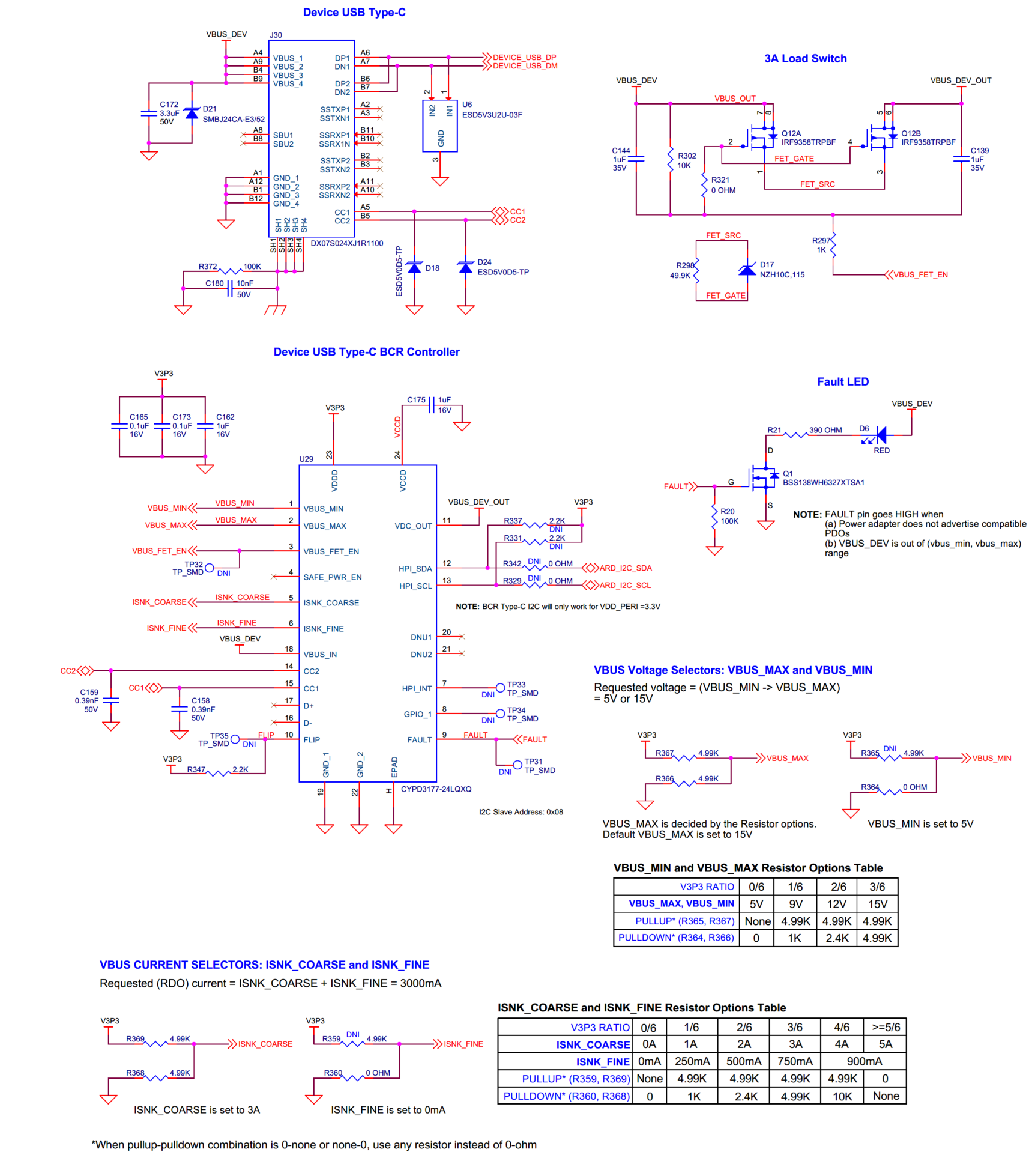
Device Type-C USB EZ-PD™ BCR controller
EZ-PD™ BCR controller for device Type-C USB power management.
The PSOC™ Edge E84 EVK features an on board CYPD3177-24LQXQ ( U29 ) EZ-PD™ Barrel Connector Replacement (BCR) controller based on the BCR product in Infineon’s USB Type-C and Power Delivery controllers. This is a highly integrated pre-programmed controller designed for power sink applications via the USB-C connector with few external components and no firmware development. The device communicates with the USB Type-C power adapter to negotiate for the proper voltage and current, as specified by on board resistors.
The controller has a red Fault LED ( D6 ) to indicate any voltage fault with the connection. If the power adapter cannot supply the power in VBUS_MIN (5 V) to VBUS_MAX (15 V) range, BCR device will turn the load switch OFF and will assert FAULT condition. Note that, the power adapter needs to have current support of 3 A for all the voltages ranging from 5 V-15 V. Else, it will trigger a fault condition.
The FAULT LED is turned ON in the following conditions:
The Device USB-C port ( J30 ) cannot provide the voltages or current requested by the system
Voltage on VBUS is 20% below the VBUS_MIN setting or 20% above the VBUS_MAX setting
Additionally, the device has an I2C slave interface which is connected to the PSOC™ Edge E84 host processor to control and monitor the EZ-PD™ BCR device. For more information, see the
EZ-PD™ BCR datasheet
.
Figure 46.
Schematic of device USB Type-C BCR controller
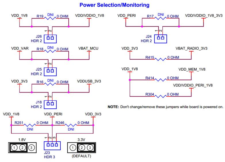
PSOC™ Edge E84 power selection and current monitoring headers
Power selection and current monitoring headers for PSOC™ Edge E84 MCU.
The PSOC™ Edge E84 MCU requires four different power domains:
VDD/VDDIO_1V8 ( J26.2 ): This is a 1.8 V power rail used to power the core and majority of I/O domains of the PSOC™ Edge E84. This domain is not used by default. Refer to the section Rework for enabling 1.8 V VDD operation of MCU to use this power domain
VDD/VDDIO_1V8_3V3 ( J24.2 ): This is a 1.8 V/3.3 V configurable (using J23 ) power rail used to power the Port 16 and Port 17 I/O domains of the PSOC™ Edge E84
VDDUSB_3V3 ( J18.2 ): This is a 3.3 V power rail used to power the VDDUSB domain of the PSOC™ Edge E84
VBAT_MCU ( J25.2 ): This is a 2.7 V/3.3 V/4.2 V configurable (using J22 ) power rail used to power the VBAT domain of the PSOC™ Edge E84. This domain is used by default
These power rails are connected through 2-pin headers ( J26 , J24 , J18 , J25 ) which can be used to enable/disable the power or current measurement of each domain of the PSOC™ Edge E84.
Apart from the MCU power, there is a VDD_PERI ( J23.2 ) power domain which is used to power some of the on board peripherals which are mainly connected to the Port 16 and Port 17 of the PSOC™ Edge E84. VDD_PERI can be configurable to 1.8 V or 3.3 V using
J23
which also configures the VDD/VDDIO_1V8_3V3 domain accordingly.
Note:
These headers (
J26
,
J24
,
J18
,
J25
,
J23
) are not recommended to change or remove while the board is powered on.
Jumper position | VDD_PERI |
|---|---|
1-2 | 1.8 V |
2-3 (Default) | 3.3 V |
There are three more power rails (VBAT_RADIO_3V3, VDD_MEM_1V8 and VDD/VDDIO_PERI_1V8) to power the other peripherals on the processor SoM (AIROC™ CYW55513 radio, memory sub-system and CAPSENSE™ co-processor) which are connected to their respective regulator outputs on the EVK through 0-ohm resistors (
R415
,
R414
and
R304
respectively). These resistors can be removed for current measurement of the respective domains by probing a with a current meter. Refer to the section 3.5 for the power monitoring setup details. Also note that, there is leakage path that need to be reworked (refer section Rework for PSOC™ Edge E84 MCU low power current measurement ) before power monitoring.
Figure 47.
Schematic of PSOC™ Edge E84 power selection and current monitoring headers
Ammeters can be connected across these jumpers
J18
(VDDUSB_3V3),
J24
(VDD/VDDIO_1V8_3V3),
J25
(VBAT_MCU),
J26
(VDD/VDDIO_1V8) to measure the current consumed by the PSOC™ Edge E84 MCU device. Remove the jumpers, connect the ammeters as shown and power the kit.
Figure 48.
Ammeter connection details for current measurement
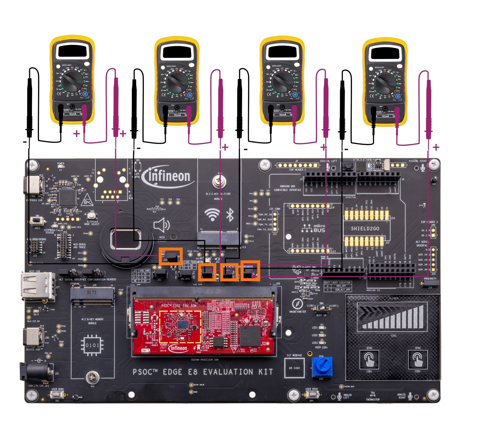
Note:
Make sure to do the rework mentioned in the section
Rework for PSOC™ Edge E84 MCU low power current measurement
before performing current measurement.
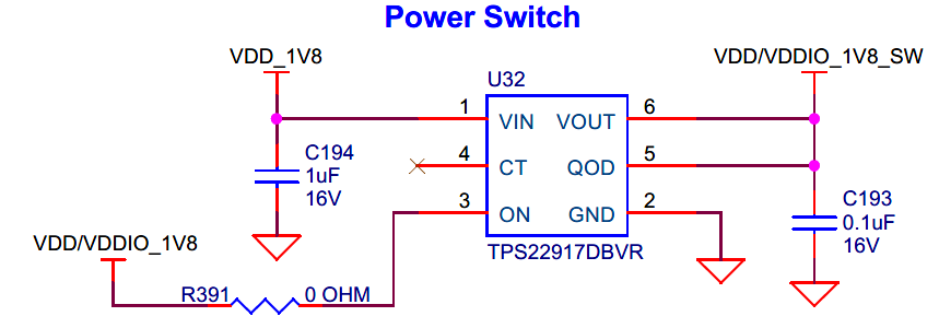
Power switch
Power switch for VTARG sense through on board KitProg3 to reduce current leakage on the power rail.
A power switch (
U32
) is provided to supply power for the VTARG_MEAS and P5LP_SIO_VREF resistor divider networks for the on board PSOC™ 5LP. The circuit is used to reduce the current leakage on the VDD/VDDIO_1V8 power domain.
Figure 49.
Schematic of power switch
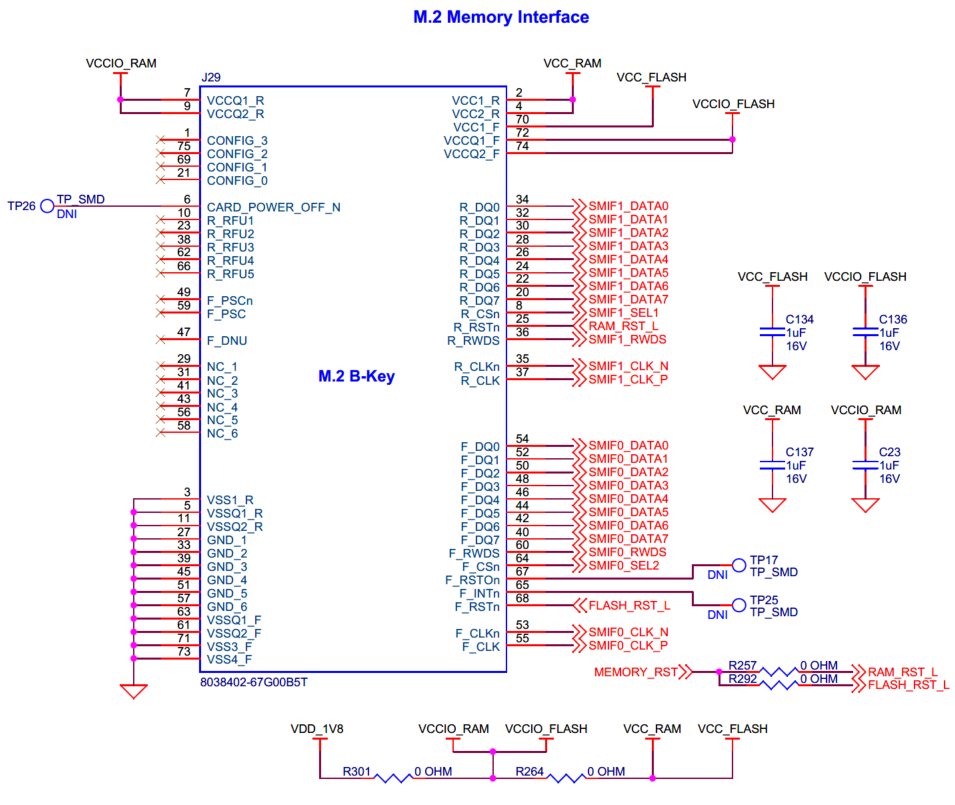
M.2 (B-Key) external memory interface
M.2 B-key memory interface for connecting external memory module.
The M.2 B-key external memory interface (
J29
) adds memory connectivity to PSOC™ Edge E84 MCU as required. The M.2 B-key memory module can be interfaced to the PSOC™ Edge E84 EVK. The external M.2 memory module comprises of a FLASH and a RAM device which are connected to the PSOC™ Edge E84 MCU using individual SMIF interface. FLASH device is connected to SMIF0 channel and RAM is connected to SMIF1 channel of the PSOC™ Edge E84 MCU. The supply for the module is provided from the 1.8 V (VDD_1V8) rail.
Note that this M.2 B-key external memory interface is not connected to the PSOC™ Edge E84 MCU by default. See
Rework for M.2 external memory interface
section for connection.
Group | Signal name | M.2 (E-Key) connector pin |
|---|---|---|
FLASH interface | SMIF0_CLK_P | 55 |
SMIF0_CLK_N | 53 | |
SMIF0_DATA0 | 54 | |
SMIF0_DATA1 | 52 | |
SMIF0_DATA2 | 50 | |
SMIF0_DATA3 | 48 | |
SMIF0_DATA4 | 46 | |
SMIF0_DATA5 | 44 | |
SMIF0_DATA6 | 42 | |
SMIF0_DATA7 | 40 | |
SMIF0_RWDS | 60 | |
SMIF0_SEL2 | 64 | |
FLASH_RST_L | 68 | |
RAM interface | SMIF1_CLK_P | 37 |
SMIF1_CLK_N | 35 | |
SMIF1_DATA0 | 34 | |
SMIF1_DATA1 | 32 | |
SMIF1_DATA2 | 30 | |
SMIF1_DATA3 | 28 | |
SMIF1_DATA4 | 26 | |
SMIF1_DATA5 | 24 | |
SMIF1_DATA6 | 22 | |
SMIF1_DATA7 | 20 | |
SMIF1_RWDS | 36 | |
SMIF1_SEL1 | 8 | |
RAM_RST_L | 25 |
Figure 50.
Schematic of M.2 (B-Key) memory interface
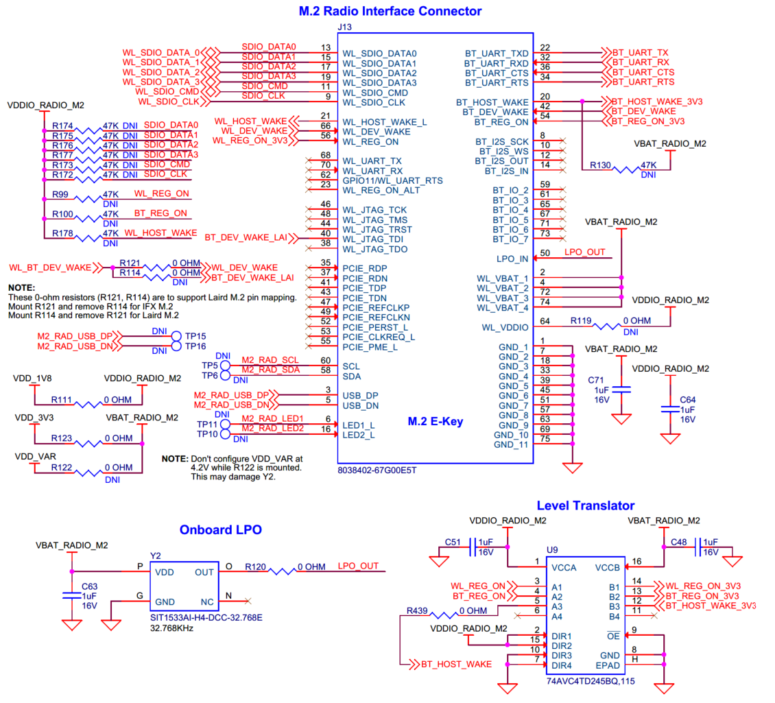
M.2 (E-Key) external radio interface
M.2 E-key radio interface for connecting external M.2 radio module.
The M.2 E-key external radio interface (
J13
) adds radio connectivity to PSOC™ Edge E84 MCU as required. Any
M.2 E-key radio module
, compatible with Infineon M.2 connector pin mapping, can be interfaced to the PSOC™ Edge E84 EVK. The WLAN interface to the PSOC™ Edge E84 MCU is SDIO and the Bluetooth® interface is UART. M.2 E-key interface also supports USB interface for the WLAN radio.
The VBAT supply (VBAT_RADIO_M2) for the module is provided from the 3.3 V (VDD_3V3) or 2.7 V-4.2 V variable power rail (VDD_VAR). VDDIO_RADIO_M2 is connected to 3.3 V (VDD_3V3) by default. It can be changed to VDD_VAR by removing
R123
and populating
R122
. On the other hand, the I/O supply (VDDIO_RADIO_M2) is provided from the 1.8 V (VDD_1V8) rail. Refer to the appropriate M.2 radio module datasheet for valid operating voltage. Also, an on-board LPO provides 32.786KHz external clock to the radio module via the M.2 interface.
Note that, this M.2 E-key external radio interface is not connected to the PSOC™ Edge E84 MCU by default. See
Rework for M.2 external radio interface
section for connection.
Group | Signal name | M.2 (E-Key) connector pin |
|---|---|---|
WLAN interface | SDIO_CLK | 9 |
SDIO_CMD | 11 | |
SDIO_DATA0 | 13 | |
SDIO_DATA1 | 15 | |
SDIO_DATA2 | 17 | |
SDIO_DATA3 | 19 | |
WL_HOST_WAKE | 21 | |
WL_REG_ON | 56 | |
WL_DEV_WAKE | 66 | |
Bluetooth® interface | BT_UART_TXD | 22 |
BT_UART_RXD | 32 | |
BT_UART_RTS | 34 | |
BT_UART_CTS | 36 | |
BT_HOST_WAKE | 20 | |
BT_DEV_WAKE | 42 | |
BT_REG_ON | 54 | |
Clock | LPO_IN | 50 |
Power | VBAT | 2, 4, 72, 74 |
WL_VDDIO (Not connected by default) | 64 |
Note:
Some modules from Laird Connectivity like Sterling-LWB5+ does not follow the Infineon M.2 interface standard. For such modules, use the resistor setting mentioned in
Rework for M.2 external radio interface
section.
Signal name | Infineon M.2 connector pin | Laird M.2 connector pin |
|---|---|---|
WL_DEV_WAKE | 66 | 42 |
BT_DEV_WAKE | 42 | 40 |
Figure 51.
Schematic of M.2 (E-Key) External Radio Interface
CAPSENSE™ interface
Capacitive buttons, slider, and shield
Capacitive buttons, 5-segment slider, and shield for EVK user interface.
The PSOC™ Edge E84 EVK has one CAPSENSE™ 5-segment slider (
CSS1
) and two CAPSENSE™ buttons (
CSB1
,
CSB2
) which are connected to the PSOC™ 4000T CAPSENSE™ Co-processor (CY8C4046LQI-T452). The CAPSENSE™ slider and buttons support both self-cap (CSD) and mutual cap (CSX) sensing modes for this kit. Note that the CAPSENSE™ shield is connected to ground by default. But it can also be configured to active shield drive mode by removing
R388
and populating
R385
. For details on using CAPSENSE™ including design guidelines, see the
PSOC™ 4 and PSOC™ 6 MCU CAPSENSE™ design guide
.
CAPSENSE™ element | PSOC™ 4000T GPIO | CAPSENSE™ element | PSOC™ 4000T GPIO |
|---|---|---|---|
CSB0 | P2[1] | CSS2 | P0[2] |
CSB1 | P2[4] | CSS3 | P0[3] |
CS_TX1 | P2[0] | CSS4 | P0[4] |
CSS0 | P0[0] | CS_TX2 | P1[0] |
CSS1 | P0[1] | CSH | P3[0] |
Figure 52.
Schematic of capacitive buttons, slider, and shield
Proximity sensor interface
Proximity sensor interface for EVK.
The PSOC™ Edge E84 EVK has an onboard proximity sense connector (
J19
) which can be used for proximity sensing applications. This pin is connected to
P4[0]
pin of the PSOC™ 4000T CAPSENSE™ co-processor (CY8C4046LQI-T452).
Figure 53.
Schematic of proximity sensor interface
I/O headers
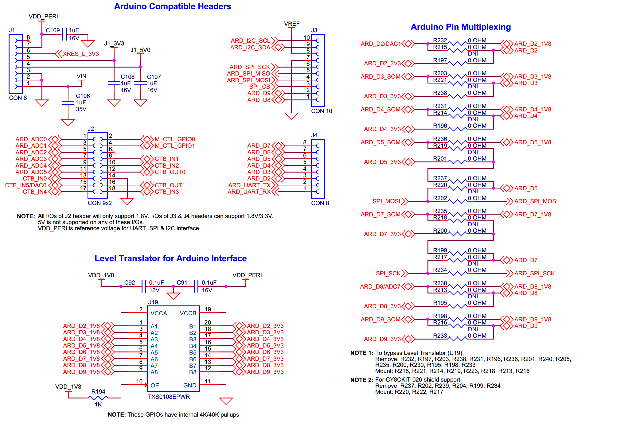
Arduino compatible headers
Arduino compatible headers for EVK.
The board has four Arduino compatible headers:
J1
,
J2
,
J3
and
J4
. You can connect Arduino compatible shields to develop applications based on the shield’s hardware. Do note that, all I/Os of
J2
header will only support 1.8 V. I/Os of
J3
and
J4
headers can support 1.8 V/3.3 V (3.3 V by default). VDD_PERI is reference voltage for UART, SPI and I2C interfaces which can be set to 1.8 V/3.3 V (3.3 V by default). 5 V is not supported on any of these I/Os and connecting a 5 V shield may permanently damage the board. The Arduino I/Os are also shared with the on board IFX Shield2Go (
J10
and
J12
) and MikroBUS Click headers (
J9
and
J17
) as well. So only one of these interfaces can be used at a time and may not work concurrently. See
Figure 3
for details on PSOC™ Edge E84 MCU pin mapping to these headers.
There are two reverse voltage protection circuits on 3.3 V (J1_3V3) and 5 V (J1_5V0) power rails connected to the Arduino power header (
J1
) as well as to mikroBUS Click headers (
J9
,
J17
) and IFX Shield2Go header (
J10
) to protect the on board peripherals and regulators from reverse voltage. The I/Os
ARD_D2
to
ARD_D9
,
ARD_I2C_SCL
and
ARD_I2C_SDA
are connected to the Arduino headers through level translators (
U19
,
U11
) using which the logic level of these I/Os can be configured to 1.8 V/3.3 V (by changing VDD_PERI from
J23
). But there is also a provision to bypass the level translators by changing the multiplexing resistors as mentioned in the
Rework for bypassing Arduino interface level translator
section. This provision is provided in case the level translators (
U19
,
U11
) fail to work at higher speeds and hence can be bypassed. Note that if the level translators are bypassed, the logic voltage of the I/Os will be as same as the MCU logic level which is 1.8 V.
The list of supported Infineon's Arduino-compatible shields are as follows:
Shield | Features not supported (if any) | Rework |
|---|---|---|
CY8CKIT-026 CAN and LIN Shield | - | Yes 5 |
CY8CKIT-028-EPD E-INK Display Shield | PDM, EPD display, IMU interrupt (optional) | No |
CY8CKIT-028-TFT TFT Display Shield | PDM, TFT display | No |
CY8CKIT-028-SENSE IoT Sense Expansion Kit | PDM, Codec, Pressure sensor interrupt (optional) | No |
CY15FRAMKIT-001 Serial F-RAM Development Kit | Write protect of FRAMs (optional) | No |
CY15FRAMKIT-002 F-RAM Development Kit | - | No |
CY8CKIT-032 PSOC™ 4 AFE Shield | LED1 control, Mechanical BTN1 read | No |
XENSIV™ Sensor Shield | PDM, IMU interrupt (optional) | No |
Figure 54.
Schematic of Arduino-compatible headers
Infineon's Shield2Go interface
Infineon’s Shield2Go interface for EVK.
The board has two headers compatible with Infineon’s Shield2Go interface (
J10
and
J12
) to support different add-on boards compatible with Infineon’s Shield2Go interface. These headers (
J10
and
J12
) are not populated by default on the board. You can connect 1.8 V/3.3 V (based on
J23
position, 3.3 V by default) Shield2go boards to develop applications. But it doesn’t support 5 V shields, so connecting a 5 V add-on board may permanently damage the board. Note that the analog I/Os (ARD_ADC0, ARD_ADC1) will only support 1.8 V and are not connected by default. Populate
R91
,
R92
to connect the analog I/Os to the header. See
Figure 3
for details on PSOC™ Edge E84 MCU pin mapping to these headers.
Note:
Recommended part MPN:
J10
→ PPPC091LFBN-RC,
J12
→ PPPC081LFBN-RC
Shield | Supply voltage | |
|---|---|---|
1 | XENSIV™ TLI4971 current sensor | 3.1 V - 3.5 V (3.3 V typical) |
2 | XENSIV™ DPS310/DPS368 pressure sensors | 1.7 V - 3.6 V (3.3 V typical) |
3 | XENSIV™ IM69D130 MEMS microphone | 3.3 V (typical), 1.8 V supported with rework |
4 | XENSIV™ BGTLTR11AIP 60 GHz radar | To be discussed |
5 | XENSIV™ TLE493D/TLI493D 3D magnetic sensor | 2.8 V - 3.5 V (3.3 V typical) |
6 | XENSIV™ TLE4966K hall effect sensor | 2.7 V - 24 V (3.3 V typical) |
7 | XENSIV™ TLE4964 hall effect sensor | 3 V - 32 V (3.3 V typical) |
8 | XENSIV™ PAS CO2 sensor | 12 V (IR Emitter), 3.3 V (Core) |
9 | S2Go Security OPTIGA™ Trust M | 3.13 V - 3.63 V (3.3 V typical) |
10 | S2Go Security OPTIGA™ E | 3.13 V - 3.63 V (3.3 V typical) |
11 | S2GO Security OPTIGA™ X | 3.13 V - 3.63 V (3.3 V typical) |
Figure 55.
Schematic of Infineon's Shield2Go interface
mikroBUS Click interface by MikroElektronika
MikroBUS Click interface for EVK.
The board has two headers compatible with mikroBUS Click interface (
J9
and
J17
) to support different add-on boards compatible with mikroBUS by MikroElektronika. These headers (
J9
and
J17
) are not populated by default on the board. You can connect 3.3 V (based on
J23
position, 3.3 V by default) mikroBUS Click add-on shields to develop applications. But it does not support 5 V shields, so connecting a 5 V add-on board may permanently damage the board. Note that the analog I/O (ARD_ADC2) will only support 1.8 V and is not connected by default. Populate
R101
to connect the analog I/O to the header. See
Figure 3
for details on PSOC™ Edge E84 MCU pin mapping to these headers.
Note:
Recommended part MPN:
J9
,
J17
→ PPPC081LFBN-RC
Figure 56.
Schematic of mikroBUS Click interface by MikroElektronika
Expansion headers
Expansion headers for EVK.
There are three expansion headers (
J6
,
J7
,
J40
) which provide connectivity to PSOC™ Edge E84 MCU GPIOs that are multiplexed with on board peripheral pins. Therefore, it is recommended to disconnect these pins from the on board peripherals before using these pins as GPIOs. For detailed information on how to rework the kit to use these pins, see
Rework for expansion headers
section. Note that these expansion headers (
J6
,
J7
,
J40
) are not loaded on board by default. See
Figure 3
for details on PSOC™ Edge E84 MCU pin mapping to these headers.
Note:
Recommended part MPN:
J6 →
PPPC081LFBN-RC,
J7
→ PPPC121LFBN-RC,
J40
→ PPPC021LFBN-RC
Figure 57.
Schematic of expansion headers
Extended I2S interface
Extended I2S interface for EVK.
There is an extended I2S header (
J11
) on the board which exposes four of the TDM[1] port I/Os which are not exposed on the Arduino compatible header. See
Figure 3
for details on PSOC™ Edge E84 MCU pin mapping to these headers. The other TDM[1] port I/Os exposed on the Arduino header (
J4
) are
ARD_D3
,
ARD_D4
,
ARD_D5
and
ARD_D7
which can be used along with these extended I2S header I/Os as an expanded I2S interface to connect to external audio shields. The extended I2S header (
J11
) is not populated on the board by default. The I/Os of this header are multiplexed with radio and Ethernet interfaces and are not connected by default. See Rework for extended I2S interface section for instruction of using this header.
Note that these I/Os are connected through an on board level translator (
U11
) which gives the provision to configure the logic level of these I/Os to 1.8 V/3.3 V by changing the VDD_PERI from
J23
. By default, the logic level is set to 3.3 V. Also, there is a provision to bypass the level translator and connect the GPIOs directly to the header.
Figure 58.
Schematic of extended I2S interface
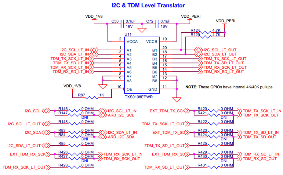
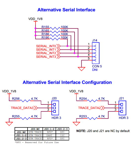
Alternative serial interface
There is an alternative serial interface header (
J14
) on board. The alternate serial interfaces allows provisioning and downloading applications using Infineon's proprietary Device Firmware Update (DFU) protocolwith the default pre-programmed version of the extended boot. This serial interface can be configured as a SPI, UART or I2C interface based on the
J20
,
J21
jumper configurations as shown in the
Table 17
. Note that these headers (
J20
,
J21
) are also used to configure the ETM TRACE interface which is set by default. The Alternative serial interface header (
J14
) is not populated by default on the board. See
Figure 3
for details on PSOC™ Edge E84 MCU pin mapping to these headers.
Note:
Recommended part MPN:
J14 →
PPTC051LFBN-RC
J20: NC | J20: 1-2 | J20: 2-3 | |
|---|---|---|---|
J21: NC | ETM TRACE (Default) | RFU* | SPI |
J21: 1-2 | ETM TRACE | UART | I2C |
J21: 2-3 | ETM TRACE | RFU* | SPI |
*RFU - Reserved for Future Use
GPIO pins are configured by extended boot as per the selected interface, as shown in the following table.
Serial interface | Serial interface pins | GPIO | J14 Connector Pin | J14 Connector pin name |
|---|---|---|---|---|
I2C | SCL | P9.3 | J14.4 | SERIAL_INT3 |
SDA | P9.2 | J14.3 | SERIAL_INT2 | |
UART | RX | P9.3 | J14.4 | SERIAL_INT3 |
TX | P9.2 | J14.3 | SERIAL_INT2 | |
SPI | SCLK | P9.3 | J14.4 | SERIAL_INT3 |
MISO | P9.1 | J14.2 | SERIAL_INT1 | |
MOSI | P9.2 | J14.3 | SERIAL_INT2 | |
SS | P9.0 | J14.1 | SERIAL_INT0 |
Figure 59.
Schematic of alternative serial interface
Audio subsystem
Audio amplifier
Audio class-D speaker driver and class A/B headphone driver for EVK.
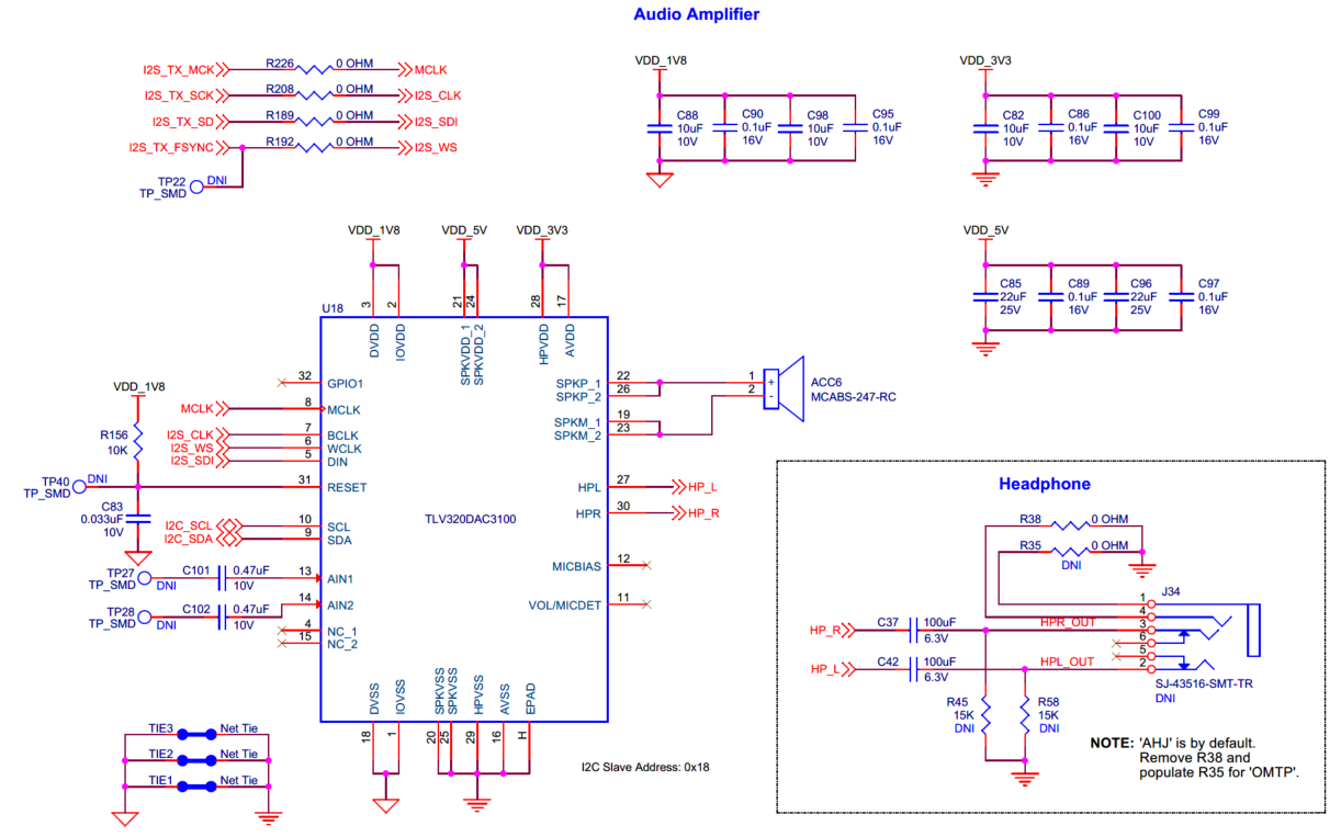
The kit contains an audio amplifier (
U18
), which is a low-power, highly integrated, high-performance stereo audio DAC with 24-bit stereo playback and digital audio processing blocks which supports of 8KHz to 192KHz sampling rates. It contains a Class-D BTL mono speaker driver and a Class A/B stereo headphone driver. The amplifier is connected to a 0.8 W, 8 Ω mono speaker (
ACC6
) and also to a headphone jack (
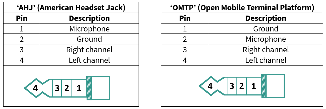
J34
) which can deliver up to 30 mW per channel into a 16 Ω load. The headphone jack (
J34
) can be configured to either AHJ (American Headset Jack) or OMTP (Open Mobile Terminal Platform) mode and is not populated by default on the board. AHJ is supported by default. See
Rework for Headphone AHJ and OMTP Modes
section for details to change it to OMTP.
Note:
Recommended part MPN:
J34
→ SJ-43516-SMT-TR
Figure 60.
AHJ and OMTP headphone configuration
Additionally, there is a pair of analog input L/R channels (
AIN1
,
AIN2
) which can be used as input for analog audio signal. The amplifier is interfaced with PSOC™ Edge E84 MCU on the EVK via an I2S interface for audio data communication and an I2C interface which provides control and full access on the registers and the state machines. The amplifier’s DVDD, IOVDD domains are supplied from 1.8 V (VDD_1V8); AVDD, HPVDD domains are supplied from 3.3 V (VDD_3V3) and SPKVDD domain from 5 V (VDD_5V). The I2C device slave address is
0x18
.
Signal name | PSOC™ Edge E84 I/O | Logic level |
|---|---|---|
MCLK | P21[3] | 1.8 V |
I2S_CLK | P21[2] | 1.8 V |
I2S_SDI | P21[1] | 1.8 V |
I2S_WS | P12[3] | 1.8 V |
Figure 61.
Schematic of audio amplifier
Analog microphones
Analog XENSIV™ MEMS microphones for EVK.
The PSOC™ Edge E84 EVK contains two analog XENSIV™ MEMS microphones (
U36
,
U37
) IM73A135V01XTSA1 from Infineon Technologies which are designed for high SNR (low self-noise) and low distortion (high AOP) applications.
U36
is the left channel microphone and
U37
being the right channel, placed ~42 mm apart from each other. Both microphones are supplied from 1.8 V (VDD_1V8) rail. The signal processing circuit for analog microphones is on PSOC™ Edge E84 SOM. Refer to section
AMIC signal processing circuit
for more details.
Signal name | PSOC™ Edge E84 I/O | Logic level |
|---|---|---|
AMIC1_INP | P14[0] | 1.8 V |
AMIC1_INN | P14[1] | 1.8 V |
AMIC2_INP | P14[4] | 1.8 V |
AMIC2_INN | P14[5] | 1.8 V |
Figure 62.
Schematic of analog microphones
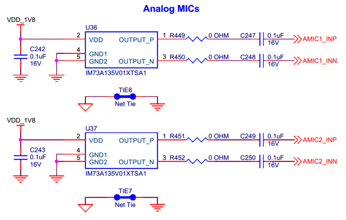
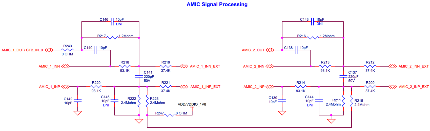
Digital microphones
Digital PDM MEMS microphones for EVK.
The PSOC™ Edge E84 EVK contains two digital PDM MEMS
microphones
(
U7
,
U8
) IM73D122V01XTMA1 from Infineon Technologies sharing the same PDM bus. Each PDM microphone has a SELECT pin; if this pin is connected to GND, the PDM data is available on the falling edge of the PDM clock. If this pin is connected to VDD, the PDM data is available on the rising edge of the PDM clock. The left PDM microphone (
U8
) data is available on the falling edge of the PDM_CLK as the SELECT pin is tied to GND. And the right PDM microphone (
U7
) data is available on the rising edge of the PDM_CLK as the SELECT pin is tied to VDD_1V8. The microphones are placed ~42 mm apart from each other and are supplied from 1.8 V (VDD_1V8) rail.
Signal name | PSOC™ Edge E84 I/O | Logic Level |
|---|---|---|
PDM_CLK | P8[5] | 1.8V |
PDM_DATA | P8[6] | 1.8V |
Figure 63.
Schematic of digital microphones
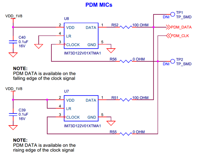
MIPI-DSI display interface
PMU section
Power management section for MIPI-DSI 10.1-inch display.
The kit has a separate power management section for the MIPI-DSI 10.1-inch display support, which consists of a DC-DC converter along with positive and negative charge pump section and an LCD backlight driver. The DC-DC converter and charge pump circuit provides the necessary voltages (exposed on J38 connector) for driving the display:
AVDD_DISP_10V2 = 10.2 V
VCOMI_DISP_4V3 = 4.3 V
VGH_DISP_20V = 20 V
VGL_DISP_-10V = -10 V
The LCD backlight driver drives the display backlight. The brightness of the display can be controlled by controlling the duty cycle of the PWM pin
BL_PWM_DISP
which is connected to the
P20[6]
pin of the PSOC™ Edge E84 MCU.
Figure 64.
Schematic of MIPI-DSI Display PMU section
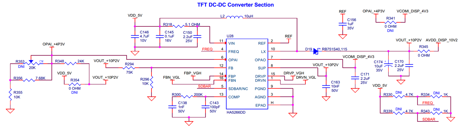
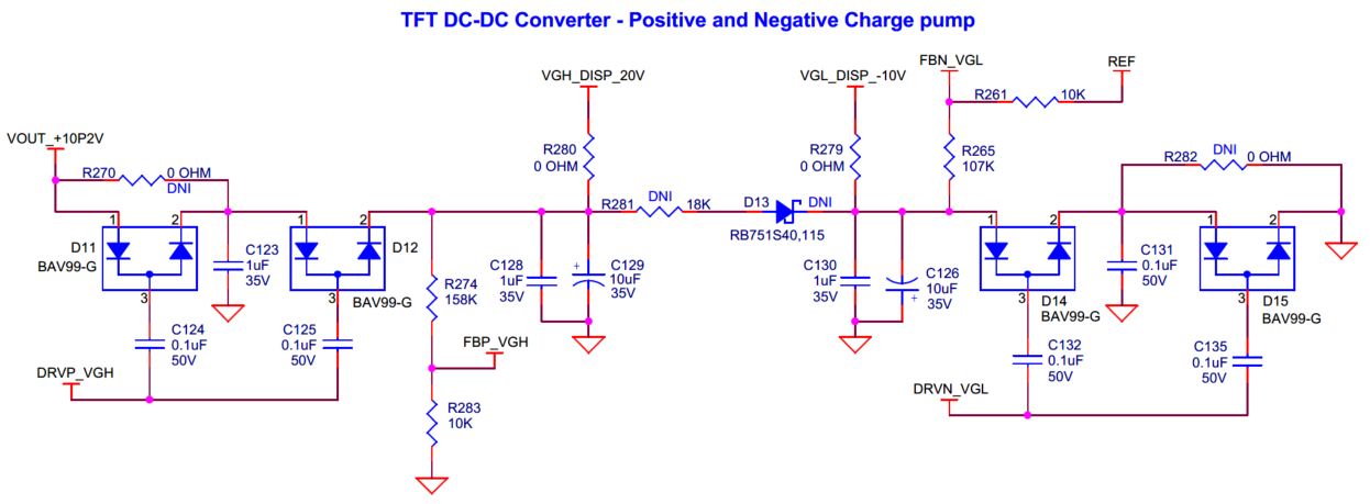
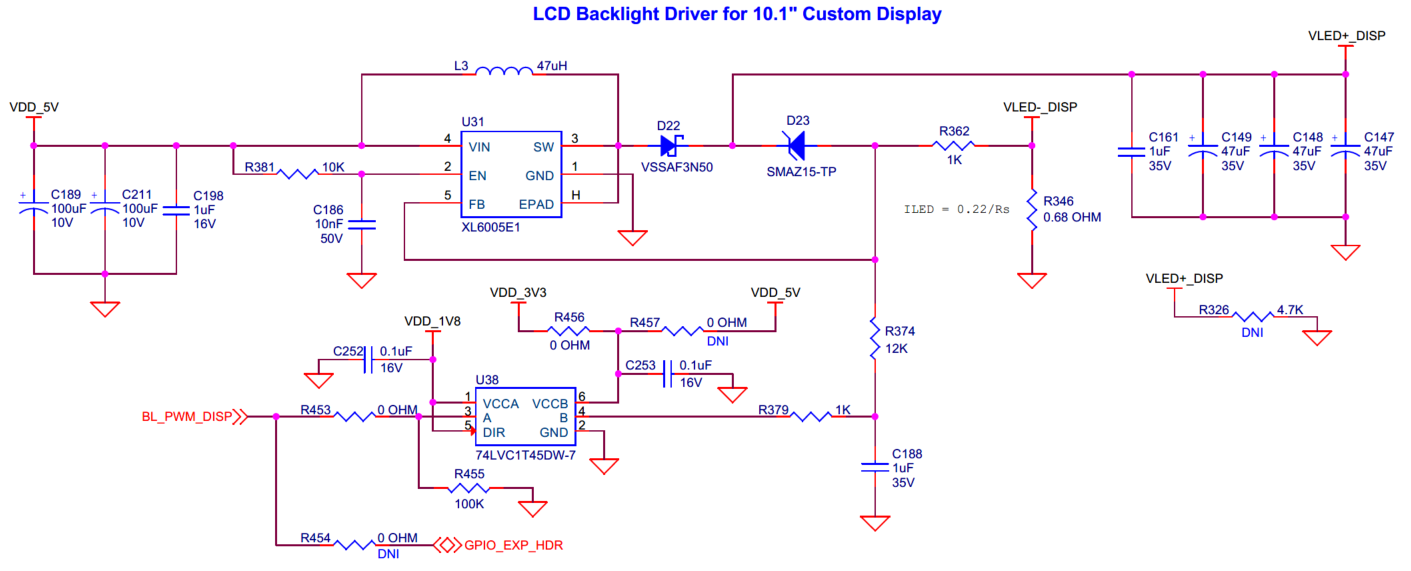
MIPI-DSI interfaces
MIPI-DSI display interfaces on EVK.
The kit has an on board MIPI-DSI display interface that supports a two-lane protocol that can go up to 1.5 Mbps speed per data lane. There are two different sets of display connectors:
MIPI-DSI custom interface ( J38 , J37 )
MIPI-DSI Raspberry-Pi interface ( J39, J41 )
The MIPI-DSI custom interface (
J38
,
J37
) supports any displays that align with this pinout. The connector
J38
is for the display driver interface and
J37
for the capacitive touch driver interface. The display control signal pin mapping with PSOC™ Edge E84 MCU is mentioned in
Table 21
.
Signal name | PSOC™ Edge E84 I/O | Logic Level |
|---|---|---|
DSI_SHLR | P21[4] | 1.8 V |
DISP_UPDN/DISP_TE | P20[5] | 1.8 V |
DISP_RST | P20[7] | 1.8 V |
DISP_STBYB | P0[0] | 1.8 V |
DISP_TP_RST | P17[3] | VDD_PERI (1.8 V/3.3 V) |
DISP_TP_INT | P17[2] | VDD_PERI (1.8 V/3.3 V) |
ARD_I2C_SCL | P8[0] | VDD_PERI (1.8 V/3.3 V) |
ARD_I2C_SDA | P8[1] | VDD_PERI (1.8 V/3.3 V) |
On the other hand, the MIPI-DSI Raspberry-Pi Interface (
J39, J41
) supports a wide range of standard Raspberry-Pi displays.
J39
is the main display interface and
J41
is the capacitive touch interface. Note that, all the Raspberry-Pi compatible displays may not need
J41
connection. Only few of them like the 7 inch MIPI-DSI 1024×600 IPS Capacitive Touch Display may need it. Refer to the
Waveshare official website
for more details. The
list of supported/recommended displays
is mentioned in
Table 22
.
Note that the MIPI-DSI custom interface and the MIPI-DSI Raspberry-Pi interface are multiplexed with each other. The MIPI-DSI Raspberry-Pi interface is connected to the PSOC™ Edge E84 MCU by default, which means only the Raspberry-Pi compatible displays will be supported natively and both 10.1-inch and 1.43-inch custom displays cannot be supported by default. To use the MIPI-DSI custom interface, see section
Rework for MIPI-DSI custom display interface
.
Note:
Although all displays listed are hardware compatible, driver support may not be available by default.
Display Type | Display Name/MPN (MFR) | Supported Through |
|---|---|---|
Custom display | 10.1 inch MIPI-DSI IPS TFT display 1024×600 with PCAP: WF101JTYAHMNB0# (Winstar) | J38 and J37 |
10.1 inch MIPI-DSI IPS TFT display 1024×600 with PCAP: WF101JSYAHMNB0# (Winstar) | ||
10.1 inch MIPI-DSI IPS TFT display 1024×600 with PCAP: MDT1010D1IHC-MIPI (Midas Displays) | ||
10.1 inch MIPI-DSI IPS TFT display 1024×600 with PCAP: RFH1010J-AYH-MNB (Raystar) | ||
1.43 inch MIPI-DSI 466×466 AMOLED+CTP display (DAS INDUSTRY LIMITED) | ||
Raspberry-Pi compatible display 6 | 2.8 inch MIPI-DSI 480×6400 Capacitive Touch Display (Waveshare) | J39 and J41 7 |
4 inch MIPI-DSI 800×480 Capacitive Touch Display (Waveshare) | ||
4.3 inch MIPI-DSI 800×480 Capacitive Touch Display (Waveshare) | ||
5 inch MIPI-DSI 800×480 Capacitive Touch Display (Waveshare) | ||
7 inch MIPI-DSI 800×480 Capacitive Touch Display (Waveshare) | ||
7 inch MIPI-DSI 1024×600 IPS Capacitive Touch Display (Waveshare) |
Figure 65.
Schematic of MIPI-DSI interface
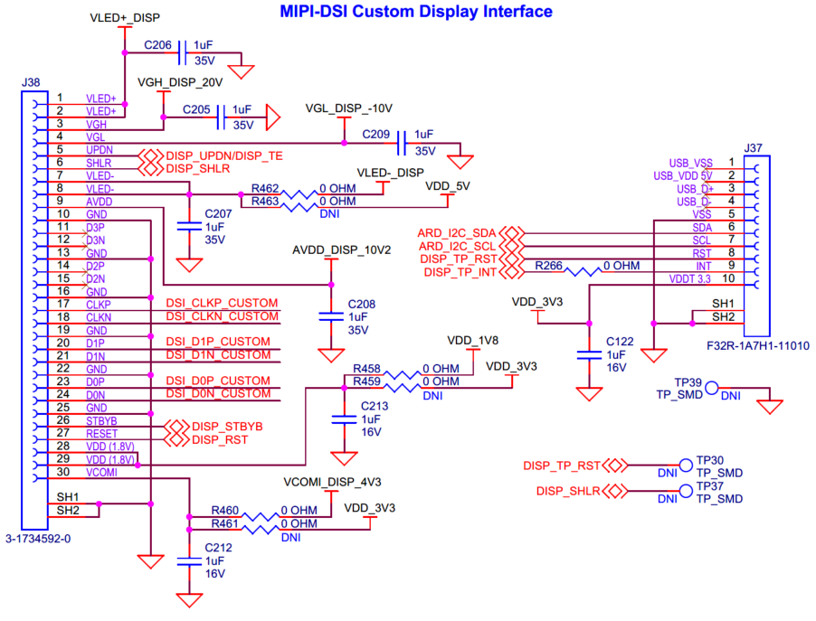
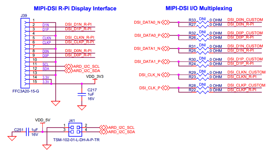
Display assembly instruction
Assembly instruction for Raspberry-Pi compatible displays and custom displays
Assembly instruction for Raspberry-Pi compatible display
The kit comes with a typical 7-inch Raspberry-Pi compatible MIPI-DSI display (1024×600) assembled by default on the baseboard. To connect a different Raspberry-Pi compatible display, follow below instructions:
Connect the FPC cable from the Display to the FPC connector
J39
on the PSOC™ Edge E8 baseboard. Notice the orientation of the FPC cable while connecting for proper contact
For displays with I2C touch interface, Insert the 4-pin female to female jumper (comes with the display bundle) into the 6-pin header on the display. Notice the orientation of the header connection as follows: Red wire to 5V, Black wire to GND, Yellow wire to SCL and White wire to SDA
Insert the other end of the 4-pin female to female jumper into the
J41
header on the baseboard. Notice the orientation of the header connection as follows: Red wire (5V) to J41.3, Black wire (GND) to J41.1, Yellow wire (SCL) to J41.2 and White wire (SDA) to J41.4
Finally, assemble the display on the baseboard using the screws and stand-offs as required
J39 and J41 on the baseboard are highlighted in the image below:
Figure 66.
Raspberry-Pi compatible display connectors
Figure 67.
Connecting the MIPI DSI interface flex cable to 15pin FPC connector
Figure 68.
Connecting the external power and I2C interface
Note:
external power and I2C interface is required only for the 7 inch MIPI-DSI Capacitive Touch Display (from Waveshare)
Assembly instruction for custom interface display
To connect a different custom MIPI interface display that supports the custom connectors, J37 and J38, follow below instructions:
Pull the drawer part of the FPC connectors J37 and J38 on the PSOC™ Edge E8 baseboard (bottom side)
Connect the 30-pin display cable from the display to the connector
J38
and connect the 10-pin touch interface cable to the connector
J37
. Notice the orientation of the FPC cable while connecting for proper contact
Push back the drawer of both the FPC connectors (J37, J38) to lock the cables
Finally, properly orient the baseboard with display as per the use-case
J37 and J38 on the baseboard are highlighted in the image below:
Figure 69.
Custom display connectors
This section no more needed
USB device
Device Type-C USB for PSOC™ Edge E84 MCU.
The board consists of a device Type-C USB (
J30
) for the PSOC™ Edge E84 MCU, which can also be used as a power source for the board, as mentioned in section Power inputs and over-voltage protection .The device USB lines are connected to the PSOC™ Edge E84 MCU by default through a USB multiplexer (
U25
). Refer to
Table 23
for USB_HOST_EN pin assignment.
Note:
Although the USB Device connector is Type-C but only USB 2.0 high speed/full speed is supported by the MCU. PD (power delivery) is supported by the
Device Type-C USB EZ-PD™ BCR controller
.
Figure 70.
Schematic of USB device
USB Host
USB Type-A Host for the PSOC™ Edge E84 MCU
The board consists of a USB Type-A Host (
J27
) for the PSOC™ Edge E84 MCU. Note that the host functionality can be enabled through firmware only (by pulling the
USB_HOST_EN
pin high) and is not enabled by default. The Host USB signals are multiplexed with the device USB signals using a USB multiplexer (
U25
). By default, the Host USB signals are not connected (the device USB is connected by default), as the default state of the
USB_HOST_EN
pin is low. Whenever a host is connected to
J27
, the USB device VBUS detect (
U26
) circuit pulls the
USB_VBUS_DET
pin high, which is then read by the PSOC™ Edge E84 MCU. Hence, the
USB_HOST_EN
pin is pulled high through the firmware to enable the host.
Do note that, the USB signals are also multiplexed using 0-ohm resistors (
R440
-
R443
) to the M.2 radio interface before it goes to the USB multiplexer (
U25
).
The board uses a USB Host VBUS Enable (
U21
,
U22
) circuit to enable the 5V (
VBUS_HOST
) output power for the host USB, which is controlled by the same
USB_HOST_EN
pin simultaneously with the USB multiplexer (
U25
). The recommended load current is 500 mA maximum from the connector. This circuit also provides an overcurrent protection (600 mA minimum, 800 mA typical) on the host USB to protect the on board regulator. Whenever an overcurrent event occurs, the
USB_FAULT
flag pin goes to a low state, which is read by the PSOC™ Edge E84 MCU. For current greater than 500 mA,
R438
can be populated to bypass the USB Host VBUS Enable (
U21
,
U22
) circuit. Note that the overcurrent protection will be disabled in that case.
Signal name | PSOC™ Edge E84 I/O | Logic Level |
|---|---|---|
USB_HOST_EN | P17[5] | VDD_PERI (1.8 V/3.3 V) |
USB_VBUS_DET | P17[4] | VDD_PERI (1.8 V/3.3 V) |
USB_FAULT | P16[4] | VDD_PERI (1.8 V/3.3 V) |
Figure 71.
Schematic of USB Host
Figure 72.
Schematic of USB Host VBUS enable circuit
Figure 73.
Schematic of USB Device VBUS detect
MicroSD card
MicroSD card for EVK
This kit contains a bottom-mounted microSD card holder (
J35
), which is connected to the SDHC[1] interface of PSOC™ Edge E84 MCU through a level translator (
U23
). The SD card works at 3.3 V logic level, which supports SDHC interface. SDHC will support up to 50 MHz of clock frequency for this kit. The card detect pin
SD_DET
is at high state by default when no SD card is inserted. Whenever the SD card is inserted, the pin changes its state to low, which is read by the PSOC™ Edge E84 MCU.
Signal name | PSOC™ Edge E84 I/O | Logic level |
|---|---|---|
SD_CLK_3V3 | P7[1] | 1.8 V (MCU side), 3.3 V (SD card side) |
SD_DATA0_3V3 | P7[3] | 1.8 V (MCU side), 3.3 V (SD card side) |
SD_DATA1_3V3 | P7[5] | 1.8 V (MCU side), 3.3 V (SD card side) |
SD_DATA2_3V3 | P7[6] | 1.8 V (MCU side), 3.3 V (SD card side) |
SD_DATA3_3V3 | P7[7] | 1.8 V (MCU side), 3.3 V (SD card side) |
SD_CMD_3V3 | P7[0] | 1.8 V (MCU side), 3.3 V (SD card side) |
SD_DET | P17[7] | VDD_PERI (1.8 V/3.3 V) |
Figure 74.
Schematic of MicroSD card
6-axis IMU (Accelerometer + Gyroscope)
6-axis IMU (Accelerometer + Gyroscope) for acceleration and gyroscopic angular rate sensing in each spatial direction.
This kit contains a 6-axis motion sensor (
U5
), also known as the inertial measurement unit (IMU), that provides precise 3-axis acceleration and 3-axis gyroscopic angular rate data in each spatial direction. The sensor uses an I2C interface to communicate along with an interrupt signal,
I2C_INT1
, which is connected to the
INT1
pin of the sensor by default. For changing the connection to the
INT2
pin of the sensor, remove
R267
and populate
R268
. The default I2C slave address is 0x68 (also configurable to 0x69 by removing
R272
and populating
R271
).
Signal name | PSOC™ Edge E84 I/O | Logic level |
|---|---|---|
I2C_INT1 | P21[7] | 1.8 V |
Figure 75.
Schematic of 6-axis IMU (Accelerometer + Gyroscope)
3-axis Magnetometer
3-axis magnetometer for geomagnetic field direction and strength sensing
This kit contains a 3-axis magnetometer sensor (
U4
) that can be used for sensing the direction and strength of the geomagnetic field. The sensor uses an I3C interface by default to communicate with the MCU. Optionally, it can also support an I2C interface (multiplexed with the I3C interface) along with an interrupt signal,
I2C_INT2
. To use the I2C interface, remove
R445
,
R447
resistors and mount the
R446
,
R448
resistors. The default I2C slave address is 0x15.
Signal name | PSOC™ Edge E84 I/O | Logic level |
|---|---|---|
I2C_INT2 | P8[4] | 1.8 V |
Figure 76.
Schematic of 3-axis Magnetometer
Potentiometer and Thermistor
Potentiometer and Thermistor for EVK
The board consists of a 10 KΩ linear potentiometer (
R34
) and a 10 KΩ NTC thermistor (
TH1
) for temperature sensing. Both sensors are capable of sensing only in single-ended mode. Note that only either of these two sensors can be used at a given time, as they are multiplexed with each other to an analog pin
P15[1]
of the PSOC™ Edge E84 MCU. The potentiometer is connected to the MCU by default. For details on how to use the thermistor, see
Rework for Thermistor
.
Signal name | PSOC™ Edge E84 I/O | Logic level |
|---|---|---|
POT/THERM | P15[1] | 1.8 V |
Figure 77.
Schematic of Potentiometer and Thermistor
User LEDs and Power LED
User LEDs and Power LED
The kit contains three discrete user LEDs:
D3
(
LED1
, red),
D4
(
LED2
, green),
D5
(
LED3
, blue), and a power LED (
D1
, yellow) for indication.
The Power LED (
D1
) The indicates that the board is powered. The user LEDs (
D3
,
D4
, and
D5
) are connected to
P16[7]
,
P16[6]
, and
P16[5]
GPIOs of the PSOC™ Edge E84 MCU, respectively. The user LEDs are active high, so the pins must be driven high to turn ON the LEDs. All the user LEDs are driven through n-MOSFETs from 3.3 V (VDD_3V3), and the gates of the MOSFETs are driven by the MCU GPIOs. Similarly, the power LED is also driven using an n-MOSFET from 3.3 V (VDD_3V3), with the gate driven by 1.8 V (VDD_1V8). Hence, the power LED will only glow when both VDD_3V3 and VDD_1V8 powers are present.
Signal name | PSOC™ Edge E84 I/O | Logic level |
|---|---|---|
USER_LED1 | P16[7] | VDD_PERI (1.8 V/3.3 V) |
USER_LED2 | P16[6] | VDD_PERI (1.8 V/3.3 V) |
USER_LED3 | P16[5] | VDD_PERI (1.8 V/3.3 V) |
Figure 78.
Schematic of User LEDs and Power LED
Reset and user buttons
Reset and user buttons on EVK.
The board contains one reset button (
SW1
) for resetting the PSOC™ Edge E84 MCU. When this
SW1
button is pressed, the
XRES_L
line of the PSOC™ Edge E84 MCU is pulled to ground, which in turn resets the target device. The reset signal is connected to the Arduino header (
J1.6
) and mikroBUS Click header (
J9.2
) as
XRES_L_3V3
through a level translator (
U16
), which configures the pin logic level to
VDD_PERI
(1.8 V/3.3 V). Do note that the pullup resistor on the
XRES_L
is populated on the PSOC™ Edge E84 SOM. Refer to
PSOC™ Edge E84 programming header
section for details.
There are also two user buttons:
SW2
(
USER BTN1
) and
SW4
(
USER BTN2
) on the board. These user buttons can be used for general user inputs or to control different states in an application. The pins
USER_SW1
and
USER_SW2
are pulled to ground when these buttons are pressed. The I/O pins used for USER_SW1 and USER_SW2 support the hibernate wake function of the PSOC™ Edge E84 MCU, allowing these buttons to be used to wake the device from hibernate mode.
Signal name | PSOC™ Edge E84 I/O | Logic level |
|---|---|---|
XRES_L | XRES | 1.8 V (XRES_L), VDD_PERI (1.8 V/3.3 V, XRES_L_3V3) |
USER_SW1 | P8[3] | 1.8 V |
USER_SW2 | P8[7] | 1.8 V |
Figure 79.
Schematic of Reset button
Figure 80.
Schematic of user buttons
Boot configuration switch
Boot configuration switch for selecting the boot location for PSOC™ Edge E84.
There is a 1-bit boot configuration DIP switch (
SW6
) that sets the boot location for the PSOC™ Edge E84 MCU. The switch output pin
BOOT
is connected to the
P17[6]
pin of the PSOC™ Edge E84, whose state is read by the MCU, and based on that, the boot location is set. See
Table 30
for the boot source options. By default, the switch position is set to 1 (OFF).
SW6 Position | Boot location |
|---|---|
0 (OFF, Default) | Internal RRAM (OEM_APP) |
1 (ON) | External FLASH (Processor SOM/M.2 Memory module) (OEM_ALT_APP) |
Figure 81.
Schematic of boot configuration switch
Ethernet subsystem
Ethernet subsystem on EVK.
The board has an on board Ethernet subsystem consisting of a low-power Ethernet PHY transceiver (
U13
) and a RJ45 MagJack (
J5
). The PHY transceiver (
U13
) supports communication with the PSOC™ Edge E84 (Ethernet MAC) via a standard MII/RMII interface. It contains a full-duplex 10-BASE-T/100BASE-TX transceiver and supports 10 Mbps (10BASE-T) or 100 Mbps (100BASE-TX) operation, having an on-chip auto-negotiation capability to automatically determine the best possible speed and duplex mode of operation. The PHY is configured to MII mode by default on the board. The VDDIO domain of the PHY is supplied from 1.8 V (VDD_1V8), and the analog port (VDD1A & VDD2A of PHY) is supplied from 3.3 V (VDD_3V3) rail. The PHY uses an on board 25 MHz crystal (
Y1
) for the MII mode and a 50 MHz crystal oscillator (
U3
) for the RMII mode operation. Note that the Ethernet I/Os are multiplexed with other on board peripheral pins and are not connected to the MCU by default. Also, the RJ45 MagJack (
J5
) is not populated by default on the board. See the
Rework for Ethernet subsystem
section for more details on the hardware configuration. There is also a PHY reset switch (
SW5
) for system reset which is not loaded by default.
Note:
Recommended part MPN:
SW5
→ SKRPACE011,
J5
→ J0011D01BNL
Signal name | PSOC™ Edge E84 I/O | Logic level |
|---|---|---|
ETH_MDIO | P13[6] | 1.8 V |
ETH_MDC | P13[1] | 1.8 V |
ETH_TX_CLK 8 | P11[5] | 1.8 V |
ETH_TXD[0] 8 | P11[2] | 1.8 V |
ETH_TXD[1] 8 | P11[3] | 1.8 V |
ETH_TXD[2] 8 | P11[6] | 1.8 V |
ETH_TXD[3] 8 | P10[0] | 1.8 V |
ETH_TX_CTL 8 | P11[4] | 1.8 V |
ETH_TX_ER 8 | P10[2] | 1.8 V |
ETH_RX_CLK 8 | P10[1] | 1.8 V |
ETH_RXD[0] 8 | P10[6] | 1.8 V |
ETH_RXD[1] 8 | P10[7] | 1.8 V |
ETH_RXD[2] 8 | P11[0] | 1.8 V |
ETH_RXD[3] 8 | P10[4] | 1.8 V |
ETH_RX_CTL 8 | P10[5] | 1.8 V |
ETH_RX_ER 8 | P11[1] | 1.8 V |
ETH_REF_CLK 8 | P11[7] | 1.8 V |
Figure 82.
Schematic of Ethernet subsystem
260-pin SODIMM connector
260-pin DDR4 SODIMM connector (
J28
) for connecting PSOC™ Edge E84 SOM.
The board consists of a 260-pin DDR4 SODIMM connector (
J28
), which is used to connect the PSOC™ Edge E84 SOM pins to the PSOC™ Edge E8 base board. It is a 0.5 mm pitch right angle connector.
Pin_Number | Signal_Name | Description |
|---|---|---|
J28.1 | CSS0 | CAPSENSE™ Slider CSS1 Segment 0 |
J28.2 | CSB1 | CAPSENSE™ CSX Button CSB2 RX |
J28.3 | CSS1 | CAPSENSE™ Slider CSS1 Segment 1 |
J28.4 | CSB0 | CAPSENSE™ CSX Button CSB1 RX |
J28.5 | CSS2 | CAPSENSE™ Slider CSS1 Segment 2 |
J28.6 | CSH | CAPSENSE™ active shield |
J28.7 | CSS3 | CAPSENSE™ Slider CSS1 Segment 3 |
J28.8 | PROXIMITY | CAPSENSE™ Proximity Sensor Input |
J28.9 | CSS4 | CAPSENSE™ Slider CSS1 Segment 4 |
J28.10 | GND | Ground |
J28.11 | GND | Ground |
J28.12 | CS_TX1 | CAPSENSE™ CSX Button CSB1, CSB2 TX |
J28.13 | CTB_IN1 | Continuous Time Block Input 1 |
J28.14 | CS_TX2 | CAPSENSE™ CSX Slider CSS1 TX |
J28.15 | CTB_IN2 | Continuous Time Block Input 2 |
J28.16 | NC | No Connect |
J28.17 | CTB_IN3 | Continuous Time Block Input 3 |
J28.18 | AMIC2_INN | Analog Microphone 2 Inverting Input |
J28.19 | CTB_IN4 | Continuous Time Block Input 4 |
J28.20 | AMIC2_INP | Analog Microphone 2 Non-Inverting Input |
J28.21 | CTB_OUTO | Continuous Time Block Output 0 |
J28.22 | CTB_INO | Continuous Time Block Input 0 |
J28.23 | CTB_OUT1 | Continuous Time Block Output 1 |
J28.24 | AMIC1_INN | Analog Microphone 1 Inverting Input |
J28.25 | M_CTL_GPIO0 | Microcontroller Control GPIO 0 |
J28.26 | AMIC1_INP | Analog Microphone 1 Non-Inverting Input |
J28.27 | M_CTL_GPIO1 | Microcontroller Control GPIO 1 |
J28.28 | GND | Ground |
J28.29 | ARD_D2_DAC1 | Arduino Digital Pin 2/DAC Channel 1 |
J28.30 | ARD_ADC5 | Arduino Analog Pin 5 |
J28.31 | CTB_IN5_DAC0 | Continuous Time Block Input 5/DAC Channel 0 |
J28.32 | ARD_ADC4 | Arduino Analog Pin 4 |
J28.33 | ARD_D8_ADC7 | Arduino Digital Pin 8/ADC Channel 7 |
J28.34 | ARD_ADC3 | Arduino Analog Pin 3 |
J28.35 | GND | Ground |
J28.36 | ARD_ADC2 | Arduino Analog Pin 2 |
J28.37 | SD_CARD_D2 | SD Card Data Line 2 |
J28.38 | ARD_ADC1 | Arduino Analog Pin 1 |
J28.39 | SD_CARD_D3 | SD Card Data Line 3 |
J28.40 | ARD_ADCO | Arduino Analog Pin 0 |
J28.41 | SD_CARD_CMD | SD Card Command Line |
J28.42 | POT_THERM | Potentiometer or Thermistor Input |
J28.43 | GND | Ground |
J28.44 | GND | Ground |
J28.45 | SD_CARD_CLK | SD Card Clock |
J28.46 | USER_LED1 | User LED 1 Control |
J28.47 | GND | Ground |
J28.48 | USER_LED2 | User LED 2 Control |
J28.49 | SD_CARD_D0 | SD Card Data Line 0 |
J28.50 | USER_LED3 | User LED 3 Control |
J28.51 | SD_CARD_D1 | SD Card Data Line 1 |
J28.52 | USER_SW1 | User Button 1 Input |
J28.53 | NC | No Connect |
J28.54 | USER_SW2 | User Button 2 Input |
J28.55 | GND | Ground |
J28.56 | GND | Ground |
J28.57 | SPI_CS | SPI Chip Select |
J28.58 | ARD_UART_TX | Arduino UART Transmit |
J28.59 | SPI_MOSI | SPI Master Out Slave In |
J28.60 | ARD_UART_RX | Arduino UART Receive |
J28.61 | SPI_MISO | SPI Master In Slave Out |
J28.62 | GND | Ground |
J28.63 | SPI_SCK | SPI Serial Clock |
J28.64 | I2C_SDA | I2C Data Line |
J28.65 | GND | Ground |
J28.66 | I2C_SCL | I2C Clock Line |
J28.67 | I3C_SCL | I3C Clock Line |
J28.68 | GND | Ground |
J28.69 | I3C_SDA | I3C Data Line |
J28.70 | NC | No Connect |
J28.71 | I2C_INT2 | I2C Interrupt 2 |
J28.72 | NC | No Connect |
J28.73 | GND | Ground |
J28.74 | GND | Ground |
J28.75 | PDM_DATA | PDM Microphone Data |
J28.76 | VREF | Reference Voltage |
J28.77 | PDM_CLK | PDM Microphone Clock |
J28.78 | GND | Ground |
J28.79 | GND | Ground |
J28.80 | DSI_DATA0_N | DSI Data Lane 0 Negative |
J28.81 | I2S_TX_MCK | I2S Transmit Master Clock |
J28.82 | DSI_DATA0_P | DSI Data Lane 0 Positive |
J28.83 | I2S_TX_SCK | I2S Transmit Serial Clock |
J28.84 | GND | Ground |
J28.85 | I2S_TX_FSYNC | I2S Transmit Frame Sync |
J28.86 | DSI_DATA1_N | DSI Data Lane 1 Negative |
J28.87 | I2S_TX_SD | I2S Transmit Serial Data |
J28.88 | DSI_DATA1_P | DSI Data Lane 1 Positive |
J28.89 | GND | Ground |
J28.90 | GND | Ground |
J28.91 | I2C_INT1 | I2C Interrupt 1 |
J28.92 | DSI_CLK_N | DSI Clock Negative |
J28.93 | GND | Ground |
J28.94 | DSI_CLK_P | DSI Clock Positive |
J28.95 | BL_PWM_DISP | Backlight PWM for Display |
J28.96 | GND | Ground |
J28.97 | DISP_STBYB | Display Standby |
J28.98 | NC | No Connect |
J28.99 | DISP_RST | Display Reset |
J28.100 | NC | No Connect |
J28.101 | DISP_TP_RST | Display Touch Panel Reset |
J28.102 | GND | Ground |
J28.103 | DISP_UPDN_DISP_TE | Display Up/Down or Tearing Effect |
J28.104 | NC | No Connect |
J28.105 | DISP_SHLR | Display Shift Left/Right |
J28.106 | NC | No Connect |
J28.107 | DISP_TP_INT | Display Touch Panel Interrupt |
J28.108 | GND | Ground |
J28.109 | GND | Ground |
J28.110 | NC | No Connect |
J28.111 | NC | No Connect |
J28.112 | NC | No Connect |
J28.113 | NC | No Connect |
J28.114 | GND | Ground |
J28.115 | NC | No Connect |
J28.116 | NC | No Connect |
J28.117 | NC | No Connect |
J28.118 | NC | No Connect |
J28.119 | NC | No Connect |
J28.120 | GND | Ground |
J28.121 | NC | No Connect |
J28.122 | NC | No Connect |
J28.123 | NC | No Connect |
J28.124 | NC | No Connect |
J28.125 | CAPSENSE_INT | CAPSENSE™ Interrupt |
J28.126 | GND | Ground |
J28.127 | ARD_D3_SOM | Arduino Digital Pin 3 (SOM) |
J28.128 | NC | No Connect |
J28.129 | ARD_D4_SOM | Arduino Digital Pin 4 (SOM) |
J28.130 | GND | Ground |
J28.131 | ARD_D5_SOM | Arduino Digital Pin 5 (SOM) |
J28.132 | VBAT_RADIO_3V3 | Radio Module Battery Voltage 3.3V |
J28.133 | ARD_D6_SOM | Arduino Digital Pin 6 (SOM) |
J28.134 | VBAT_RADIO_3V3 | Radio Module Battery Voltage 3.3V |
J28.135 | GND | Ground |
J28.136 | VBAT_RADIO_3V3 | Radio Module Battery Voltage 3.3V |
J28.137 | WL_SDIO_CLK | Wireless SDIO Clock |
J28.138 | VBAT_RADIO_3V3 | Radio Module Battery Voltage 3.3V |
J28.139 | GND | Ground |
J28.140 | VBAT_MCU | MCU Battery Voltage |
J28.141 | WL_SDIO_CMD | Wireless SDIO Command |
J28.142 | VBAT_MCU | MCU Battery Voltage |
J28.143 | GND | Ground |
J28.144 | VBAT_MCU | MCU Battery Voltage |
J28.145 | WL_SDIO_DATA_0 | Wireless SDIO Data Line 0 |
J28.146 | GND | Ground |
J28.147 | WL_SDIO_DATA_1 | Wireless SDIO Data Line 1 |
J28.148 | SERIAL_INTO | Serial Interface Input 0 |
J28.149 | WL_SDIO_DATA_2 | Wireless SDIO Data Line 2 |
J28.150 | SERIAL_INT1 | Serial Interface Interrupt 1 |
J28.151 | WL_SDIO_DATA_3 | Wireless SDIO Data Line 3 |
J28.152 | SERIAL_INT2 | Serial Interface Interrupt 2 |
J28.153 | GND | Ground |
J28.154 | SERIAL_INT3 | Serial Interface Interrupt 3 |
J28.155 | ETH_REF_CLK | Ethernet Reference Clock |
J28.156 | GND | Ground |
J28.157 | GND | Ground |
J28.158 | SD_CARD_DET | SD Card Detect |
J28.159 | BT_UART_TX_ETH_RX_CLK | Bluetooth UART Transmit/Ethernet Receive Clock |
J28.160 | BOOT | Boot Control Signal |
J28.161 | GND | Ground |
J28.162 | GND | Ground |
J28.163 | BT_UART_RTS_ETH_CMP_VAL | Bluetooth® UART Request to Send/Ethernet Comparator Value |
J28.164 | VDD_VDDIO_1V8 | Digital I/O Power Supply 1.8V |
J28.165 | BT_HOST_WAKE_ETH_RXD_3 | Bluetooth Host Wake/Ethernet Receive Data 3 |
J28.166 | VDD_VDDIO_1V8 | Digital I/O Power Supply 1.8V |
J28.167 | BT_REG_ON_ETH_RXD_2 | Bluetooth Regulator On/Ethernet Receive Data 2 |
J28.168 | VDD_VDDIO_1V8 | Digital I/O Power Supply 1.8V |
J28.169 | ETH_RXD_1 | Ethernet Receive Data 1 |
J28.170 | VDD_VDDIO_PERI_1V8 | Peripheral Digital I/O Power Supply 1.8V |
J28.171 | BT_DEV_WAKE_ETH_RXD_0 | Bluetooth Device Wake/Ethernet Receive Data 0 |
J28.172 | VDD_VDDIO_PERI_1V8 | Peripheral Digital I/O Power Supply 1.8V |
J28.173 | ETH_RX_ER | Ethernet Receive Error |
J28.174 | VDD_VDDIO_PERI_1V8 | Peripheral Digital I/O Power Supply 1.8V |
J28.175 | ETH_MDIO | Ethernet Management Data Input/Output |
J28.176 | GND | Ground |
J28.177 | ETH_MDC | Ethernet Management Data Clock |
J28.178 | VDDUSB_3V3 | USB Power Supply 3.3V |
J28.179 | BT_UART_CTS_ETH_TX_ER | Bluetooth UART Clear to Send/Ethernet Transmit Error |
J28.180 | VDD_VDDIO_1V8_3V3 | Digital I/O Power Supply 1.8V/3.3V |
J28.181 | GND | Ground |
J28.182 | VDD_VDDIO_1V8_3V3 | Digital I/O Power Supply 1.8V/3.3V |
J28.183 | ETH_TX_CLK | Ethernet Transmit Clock |
J28.184 | GND | Ground |
J28.185 | GND | Ground |
J28.186 | UART_RTS | Universal Asynchronous Receiver Transmitter Request To Send |
J28.187 | WL_HOST_WAKE_ETH_TX_CTL | Wireless Host Wake/Ethernet Transmit Control |
J28.188 | UART_CTS | Universal Asynchronous Receiver Transmitter Clear To Send |
J28.189 | WL_BT_DEV_WAKE_ETH_TXD_0 | Wireless/Bluetooth Device Wake/Ethernet Transmit Data 0 |
J28.190 | UART_RX | Universal Asynchronous Receiver Transmitter Receive |
J28.191 | ETH_TXD_1 | Ethernet Transmit Data 1 |
J28.192 | UART_TX | Universal Asynchronous Receiver Transmitter Transmit |
J28.193 | WL_REG_ON_ETH_TXD_2 | Wireless Regulator On/Ethernet Transmit Data 2 |
J28.194 | GND | Ground |
J28.195 | BT_UART_RX_ETH_TXD_3 | Bluetooth UART Receive/Ethernet Transmit Data 3 |
J28.196 | ARD_D7_SOM | Arduino Digital Pin 7 (SOM) |
J28.197 | ETH_RX_CTL | Ethernet Receive Control |
J28.198 | ARD_D9_SOM | Arduino Digital Pin 9 (SOM) |
J28.199 | GND | Ground |
J28.200 | GND | Ground |
J28.201 | TMS_SWDIO | JTAG Test Mode Select/SWD IO |
J28.202 | XRES_L | External Reset (Active Low) |
J28.203 | TCLK_SWCLK | JTAG Test Clock/SWD Clock |
J28.204 | USB_FAULT | USB Fault Status |
J28.205 | GND | Ground |
J28.206 | USB_DEV_DET | USB Device Detection |
J28.207 | TDO_SWO | JTAG Test Data Out/Serial Wire Output |
J28.208 | USB_HOST_EN | USB Host Enable |
J28.209 | TDI | JTAG Test Data In |
J28.210 | GND | Ground |
J28.211 | GND | Ground |
J28.212 | USB_DM | USB differential data line minus |
J28.213 | TRACE_CLK | Trace Debug Clock |
J28.214 | USB_DP | USB differential data line plus |
J28.215 | GND | Ground |
J28.216 | GND | Ground |
J28.217 | TRACE_DATA0 | Trace Debug Data 0 |
J28.218 | VDD_MEM_1V8 | Memory Power 1.8V |
J28.219 | TRACE_DATA1 | Trace Debug Data 1 |
J28.220 | VDD_MEM_1V8 | Memory Power 1.8V |
J28.221 | TRACE_DATA2 | Trace Debug Data 2 |
J28.222 | GND | Ground |
J28.223 | TRACE_DATA3 | Trace Debug Data 3 |
J28.224 | SMIF0_SEL2 | SMIF Flash Output Select 2 |
J28.225 | GND | Ground |
J28.226 | GND | Ground |
J28.227 | SMIF0_RWDS | SMIF Flash Output Ready/Write Data Strobe |
J28.228 | SMIF0_DATA0 | SMIF Flash Output Data 0 |
J28.229 | GND | Ground |
J28.230 | SMIF0_DATA1 | SMIF Flash Output Data 1 |
J28.231 | SMIF1_CLK_N | SMIF1 Flash Clock Negative |
J28.232 | SMIF0_DATA3 | SMIF Flash Output Data 3 |
J28.233 | SMIF1_CLK_P | SMIF1 Flash Clock Positive |
J28.234 | SMIF0_DATA5 | SMIF Flash Output Data 5 |
J28.235 | GND | Ground |
J28.236 | SMIF0_DATA7 | SMIF Flash Output Data 7 |
J28.237 | SMIF0_CLK_N | SMIF Flash Output Clock Negative |
J28.238 | GND | Ground |
J28.239 | SMIF0_CLK_P | SMIF Flash Output Clock Positive |
J28.240 | SMIF1_SEL1 | SMIF1 Flash Select 1 |
J28.241 | GND | Ground |
J28.242 | GND | Ground |
J28.243 | SMIF0_DATA2 | SMIF Flash Output Data 2 |
J28.244 | MEMORY_RST | Memory Reset |
J28.245 | SMIF0_DATA4 | SMIF Flash Output Data 4 |
J28.246 | GND | Ground |
J28.247 | SMIF0_DATA6 | SMIF Flash Output Data 6 |
J28.248 | SMIF1_DATA7 | SMIF1 Flash Data 7 |
J28.249 | GND | Ground |
J28.250 | SMIF1_DATA6 | SMIF1 Flash Data 6 |
J28.251 | SMIF1_RWDS | SMIF1 Ready/Write Data Strobe |
J28.252 | SMIF1_DATA5 | SMIF1 Flash Data 5 |
J28.253 | GND | Ground |
J28.254 | SMIF1_DATA3 | SMIF1 Flash Data 3 |
J28.255 | SMIF1_DATA2 | SMIF1 Flash Data 2 |
J28.256 | SMIF1_DATA1 | SMIF1 Flash Data 1 |
J28.257 | SMIF1_DATA4 | SMIF1 Flash Data 4 |
J28.258 | SMIF1_DATA0 | SMIF1 Flash Data 0 |
J28.259 | GND | Ground |
J28.260 | GND | Ground |
I2C device addresses
List of I2C addresses of the devices on EVK.
Device | Location on EVK | Reference designator | I2C address (7-bit hex) |
|---|---|---|---|
PSOC™ 4000T (CY8C4046LQI-T452) | PSOC™ Edge E84 SOM | U9 | 0x08 |
BCR Controller (CYPD3177-24LQXQ) | PSOC™ Edge E8 base board | U29 | 0x08* |
Audio amplifier (TLV320DAC3100) | PSOC™ Edge E8 base board | U18 | 0x18 |
6-axis IMU (BMI270) | PSOC™ Edge E8 base board | U5 | 0x68 (default)/0x69 |
Magnetometer (BMM350) | PSOC™ Edge E8 base board | U4 | 0x15** |
4.3 inch MIPI-DSI 800×480 Capacitive Touch Display | PSOC™ Edge E8 base board | N/A | 0x38, 0x45*** |
Note:
The BCR Controller I2C lines are not connected by default on the board
The magnetometer is interfaced with the MCU in I3C mode by default. The device address specified is applicable only when operating in I2C mode
For the 4.3 inch MIPI-DSI 800×480 capacitive touch display, two I2C device addresses are used: 0x38 for the touch controller and 0x45 for the display controller
PSOC™ Edge E84 kit rework
Rework instructions for PSOC™ Edge E84 kit.
Note:
All the rework instructions are made considering the kit at its default hardware setting. This instruction may not be valid for an already reworked kit.
Rework for M.2 external memory interface
This section explains the rework for enabling the M.2 external memory interface.
The PSOC™ Edge E84 MCU device's SMIF0 (Flash) and SMIF1 (RAM) channels are multiplexed with an on board memory (default) and M.2 memory board, which is present in the baseboard. You need to isolate the on board connection to operate with an external M.2 memory module. You need to mount the below showed DNI components and need to remove the stuff components. For example, for SMIF0_DATA0, remove R35 and mount R37 with 33 Ω resistor. In addition to this rework, remove
R137
,
R141
and mount
R131
,
R130
with the zero ohms.
Function | Remove | Mount | Purpose | MPN (for mounting) |
|---|---|---|---|---|
Route SMIF0 data/clock lines to M.2 connector | R35, R39, R43, R47, R51, R55, R59, R63, R68, R71, R74 | R37, R41, R45, R49, R53, R57, R61, R65, R69, R73, R76 | Disconnects SMIF0 lines from on board memory and connects them to M.2 socket. | 33 Ω resistor, RC0402FR-0733RL or equivalent |
Switch SMIF0 select signal to external M.2 | R137 | R130 | Disconnects SMIF0_SEL0 from on board memory and connects to external M.2 memory module. | 0 Ω resistor, RC0402FR-070RL or equivalent |
Function | Remove | Mount | Purpose | MPN (for mounting) |
|---|---|---|---|---|
Route SMIF1 data/clock lines to M.2 connector | R34, R38, R42, R46, R50, R54, R58, R62, R66, R70, R75 | R36, R40, R44, R48, R52, R56, R60, R64, R67, R72, R77 | Disconnects SMIF1 lines from onboard memory and connects them to M.2 socket. | 33 Ω resistor, RC0402FR-0733RL or equivalent |
Switch SMIF1 select signal to external M.2 | R141 | R131 | Disconnects SMIF1_SEL2 from onboard memory and connects to external M.2 memory module. | 0 Ω resistor, RC0402FR-070RL or equivalent |
Figure 83.
Rework regions on SoM
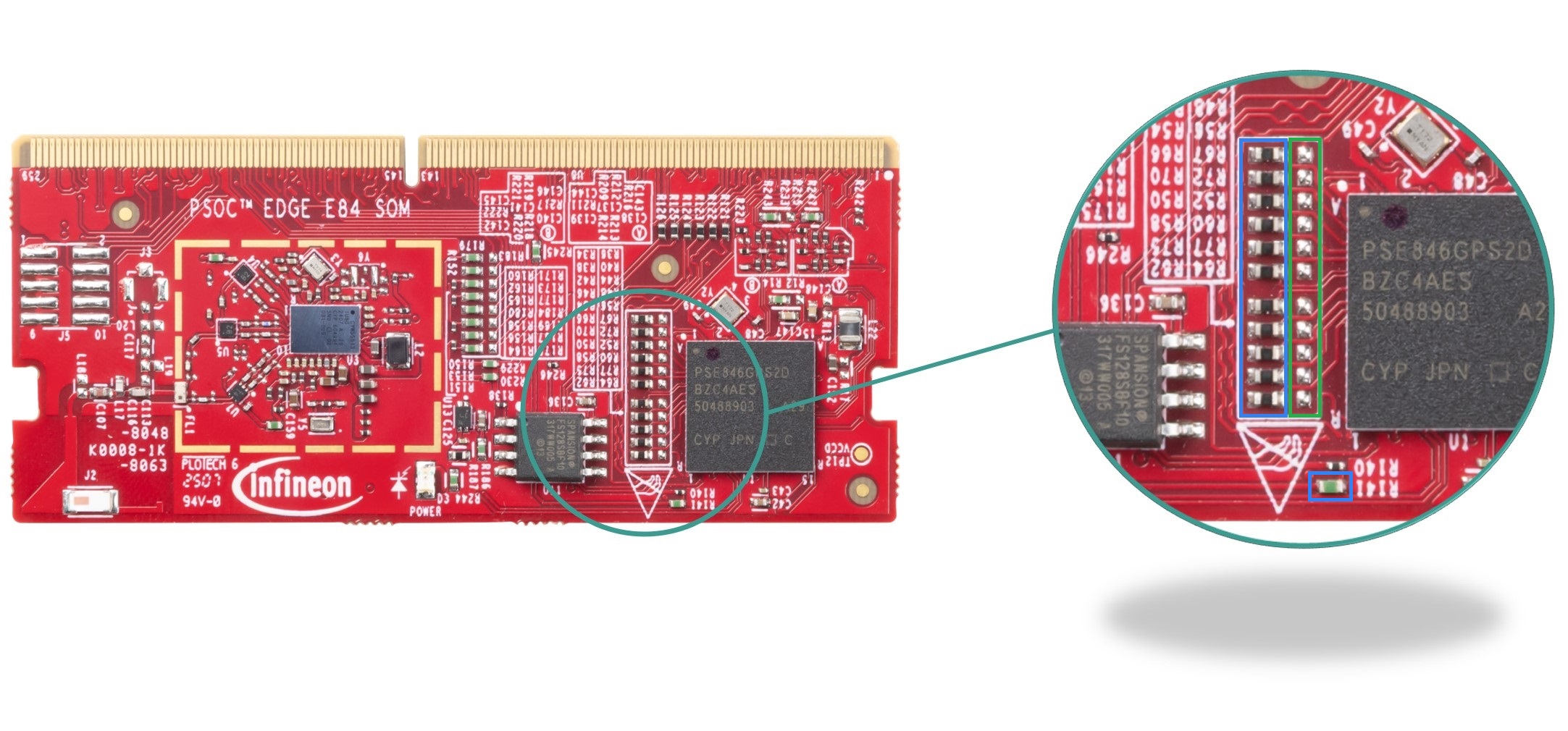
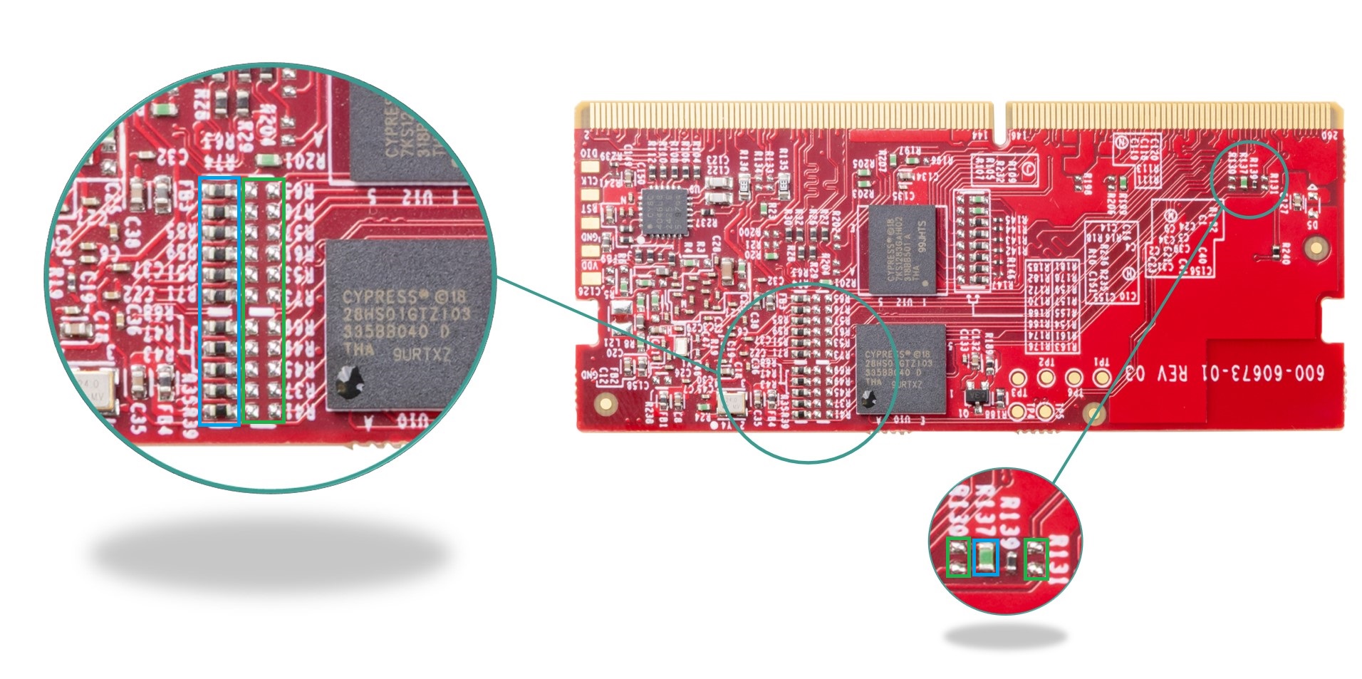
Note:
Removed parts locations are highlighted with blue and parts to be mounted are highlighted with green.
Rework for M.2 external radio interface
This section explains the rework instruction for M.2 external radio Interface.
To support the M.2 external radio interface (with the Infineon's M.2 E-key radio module ), do the following rework on processor SoM:
PSOC™ Edge E84 MCU device has a single Bluetooth® UART and SDIO0 channel that have a Y connection with the on board AIROC™ CYW55513 and the external M.2 radio module that is present in the baseboard
Remove the below DNI parts that are not shown and mount the parts that has a DNI property
Function | Remove | Mount | Purpose | MPN (for mounting) |
|---|---|---|---|---|
Switch SDIO data lines to external M.2 radio | R154, R155, R157, R159, R161, R163 | R166, R168, R170, R172, R174, R176 | Routes SDIO signals from on board radio to M.2 radio module. | 33 Ω resistor, RC0402FR-0733RL or equivalent |
Switch BT/WL wake and control signals to M.2 radio | R156, R158, R160, R162, R164, R165 | R167, R169, R171, R173, R175, R177 | Routes BT/WL/Host signals from on board radio to M.2 module. | 0 Ω resistor, RC0402FR-070RL or equivalent |
Switch BT UART signals to M.2 radio module | R178, R179, R180, R181 | R182, R183, R184, R185 | Routes UART TX/RX/CTS/RTS from on board radio to M.2 radio module. | 0 Ω resistor, RC0402FR-070RL or equivalent |
Figure 84.
WLAN and Bluetooth® rework_1 region on SoM

Note:
Parts removed locations are highlighted with blue and parts to be mounted are highlighted with green.
Figure 85.
WLAN and Bluetooth® rework_2 region on SoM
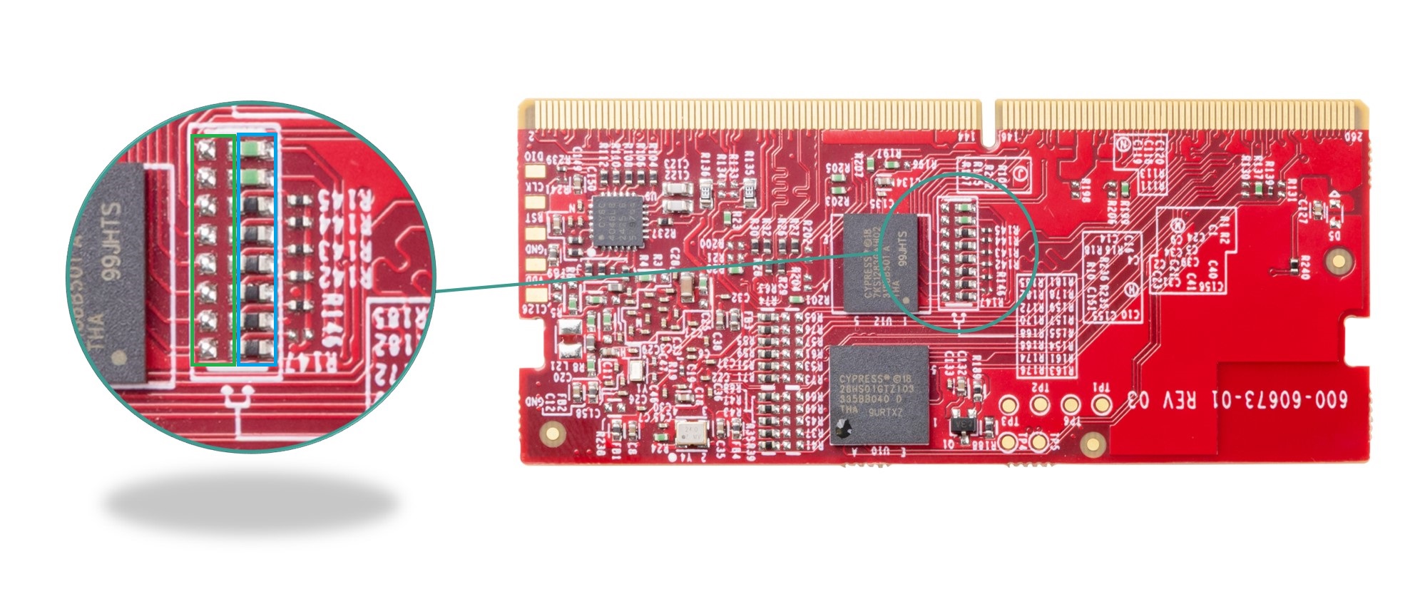
Note:
Parts removed locations are highlighted with blue and parts to be mounted are highlighted with green.
To support M.2 Laird module, do the following rework on PSOC™ Edge E8 baseboard
Function | Remove | Mount | Purpose | MPN (for mounting) |
|---|---|---|---|---|
Change WL_BT_DEV_WAKE routing for Laird module | R121 | R114 | Connects BT_DEV_WAKE_LAI signal, disconnecting former path. | 0 Ω resistor, ERJ-3GEY0R00V or equivalent |
Figure 86.
Rework region on baseboard for M.2 Laird module support
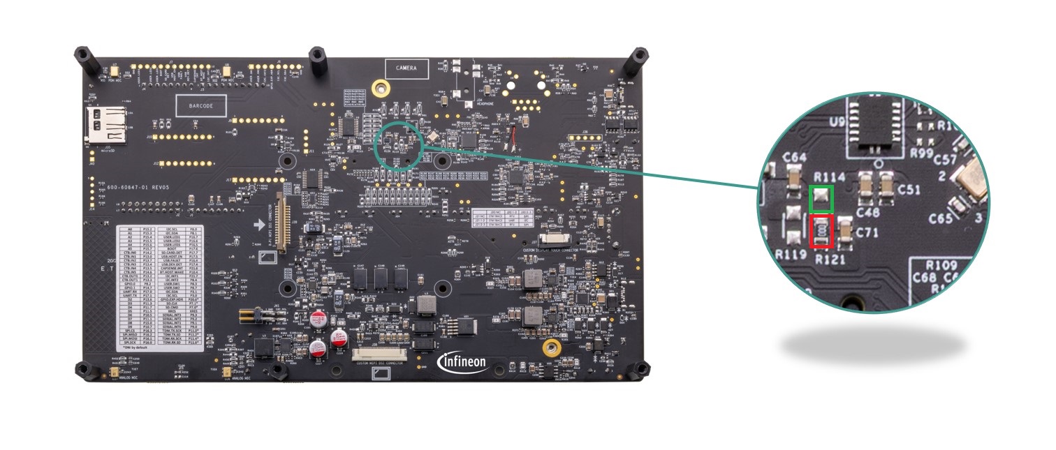
Note:
Removed parts locations are highlighted with red and parts to be mounted are highlighted with green.
Rework for enabling external antenna interface
External antenna can be connected to the SoM by changing the below rework
To enable the connection of an external antenna on the SoM, rework is necessary to route the RF path from the on board chip antenna to the uFL connector. This is accomplished by removing the component that connects to the on-board chip antenna and populating dedicated capacitors, inductors, and the uFL connector. These changes ensure a reliable RF path for external antenna operation and disconnect the default on board antenna.
Function | Remove | Mount | Purpose | MPN (for mounting) |
|---|---|---|---|---|
Disconnect chip antenna | C113 | — | Disconnects on board chip antenna to allow external antenna use. | — |
Enable uFL antenna path (RF routing/matching) | — | C116, C117, L19, L20 | Completes RF path and matching for uFL connector. | Values will be derived based matching requirement of external antenna |
Physical external antenna connection | — | J3 | Provides the uFL connecter for external antenna. | J3: A-1JB (from Amphenol) or equivalent |
Figure 87.
Rework on SoM for enabling external antenna interface
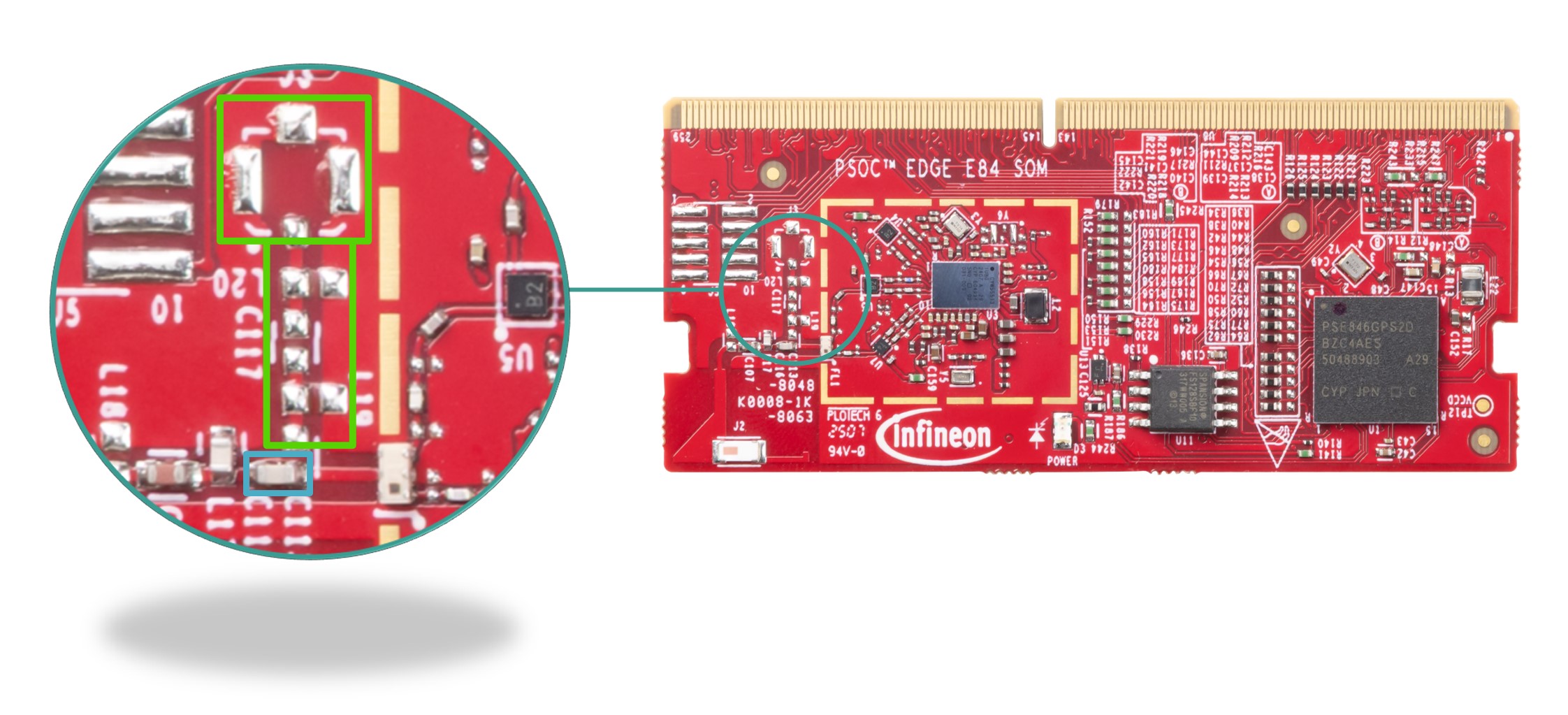
Note:
Removed parts locations are highlighted with blue and parts to be mounted are highlighted with green
Rework for enabling 1.8 V VDD operation of MCU
Rework instructions to enable 1.8 V VDD supply operation for the PSOC™ Edge E84 MCU.
PSOC™ Edge E84 MCU device can operate with a 1.8 V regulated power supply or with an external battery supply from 2.7 V to 4.2 V. In this hardware, 3.3 V VBAT supply is set by default. To change it to 1.8 V VDD supply, follow the rework below.
Function | Remove | Mount | Purpose | MPN (for mounting) |
|---|---|---|---|---|
Disconnect 3.3V VBAT path | R1, R4, R5, R8, R10, R14, R18, R236 | — | Isolates the 3.3 V supply from MCU power rails for 1.8 V operation. | — |
Disconnect VOUT_VBAT Output | L22 | — | Disables 3.3 V supply to MCU for low-voltage configuration. | — |
Connect 1.8V VDD supply path | — | R2, R3, R6, R12, R13, R16, R17, R235 | Enables 1.8 V supply to all MCU VDD pins. | Use 0 Ω resistor: RC0402FR-070RL or equivalent |
Enable 1.8V supply to MCU | — | L21 | Establishes the inductor path for 1.8 V to the MCU supply input. | LQM2MPN2R2MG0L |
Figure 88.
1.8 V VDD Rework 1 on SOM
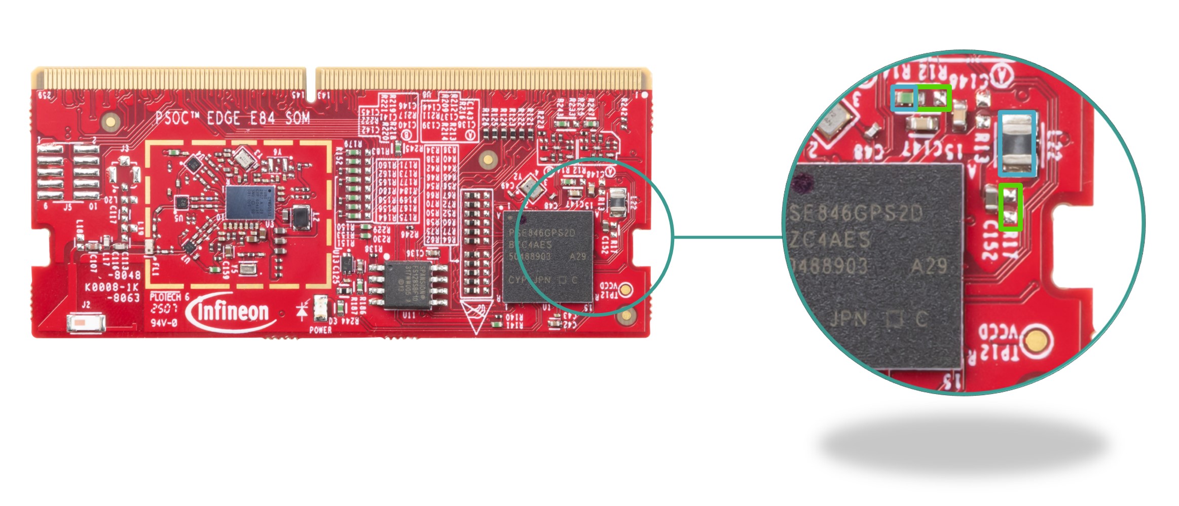
Note:
Removed parts locations are highlighted with blue and parts to be mounted are highlighted with green
Figure 89.
1.8 V VDD Rework 2 on SOM
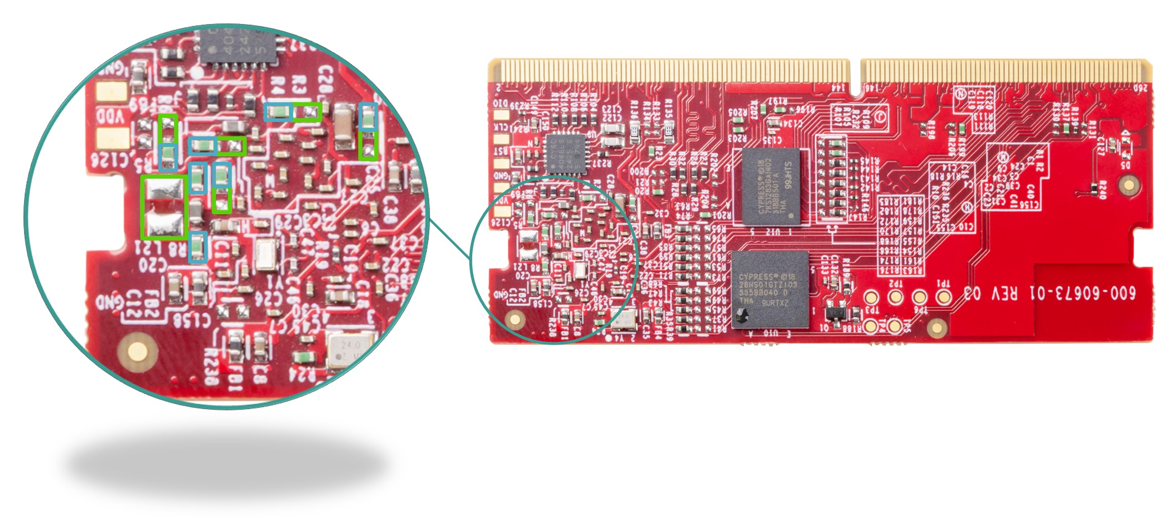
Note:
Removed parts locations are highlighted with blue and parts to be mounted are highlighted with green
Rework for Ethernet subsystem
Rework instruction for Ethernet sub-system on EVK.
Rework for MII mode
Rework instructions for Ethernet MII mode.
To enable the Ethernet MII interface on the PSOC™ Edge E84 SOM, it is necessary to rework specific resistors that multiplex the Arduino interface signals, Extended I2S, and Ethernet signals. After performing this rework, only the Ethernet interface will be available; the Arduino and Extended I2S interfaces will be disabled.
Function | Remove | Mount | Purpose | MPN (for mounting) |
|---|---|---|---|---|
Switch shared MCU/Arduino/I2S pins to Ethernet operation | R207, R197, R205, R199, R20, R201, R203, R156, R158, R160, R162, R164, R165, R178, R179, R180, R181 | R206, R196, R204, R198, R21, R200, R202, R167, R169, R171, R173, R175, R177, R182, R183, R184, R185 | Moves all multiplexed signals from Arduino, I2S, and Bluetooth/Radio functions to Ethernet interface; disables other modes and enables full MII Ethernet subsystem functionality. | 0 Ω resistor, RC0402FR-070RL or equivalent |
Figure 90.
Rework region on SoM for Enabling Ethernet MII Mode
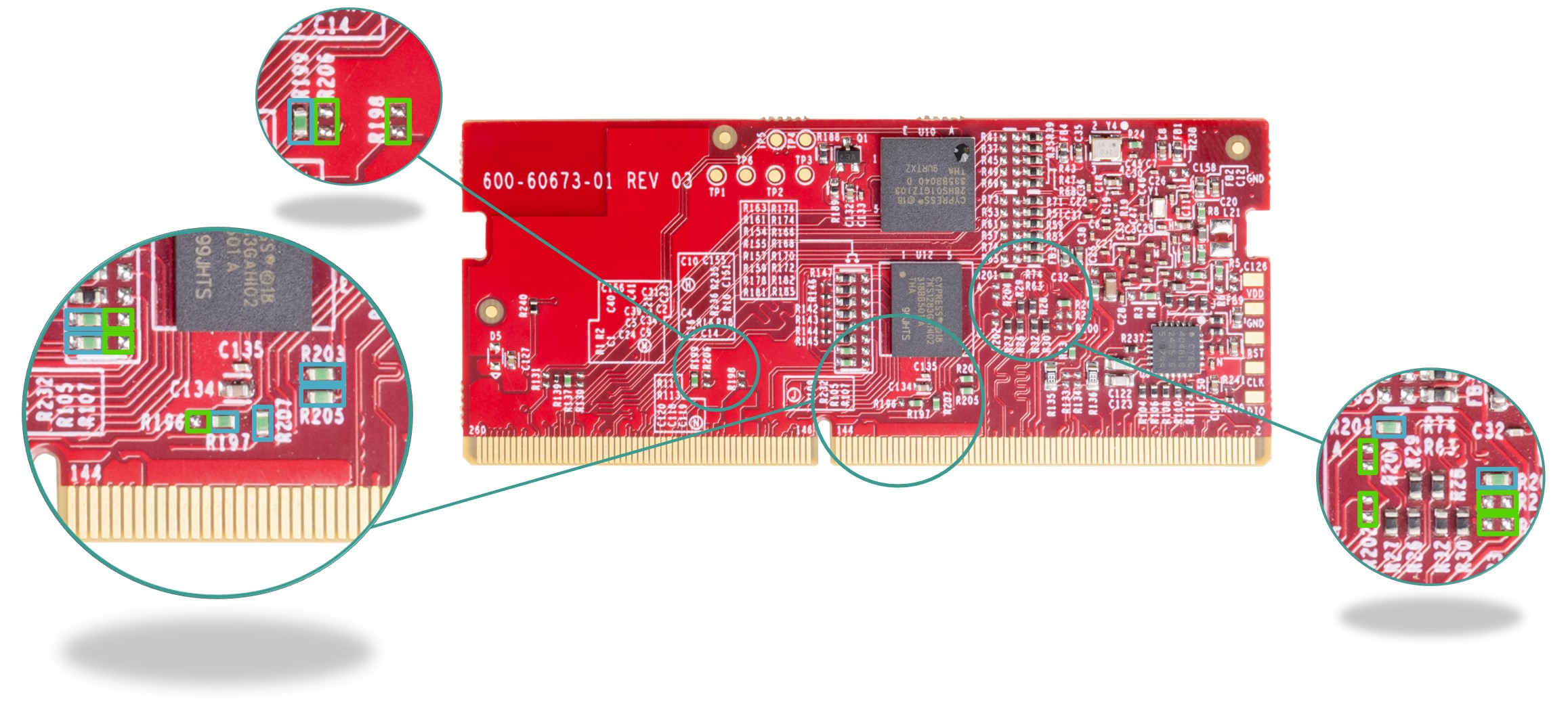
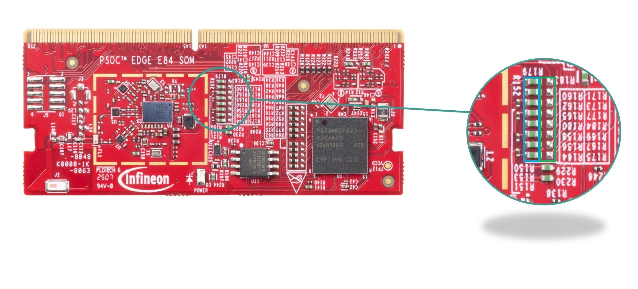
Note:
Removed parts locations are highlighted with blue and parts to be mounted are highlighted with green
Function | Remove | Mount | Purpose | MPN (for mounting) |
|---|---|---|---|---|
Switch multiplexed I/O to Ethernet subsystem | R171, R167, R169, R166, R168, R67, R69, R68, R70 | R185, R181, R183, R180, R182, R78, R80, R79, R81 | Moves shared signals to the Ethernet subsystem, enabling full MII functionality on the baseboard. | 0 Ω resistor, ERJ-3GEY0R00V or equivalent |
Enable Ethernet physical connector | — | J5 | Populates Ethernet RJ45 connector on the baseboard for physical network connection. | J5: J0011D01BNL or equivalent |
Figure 91.
Rework region on baseboard for enabling Ethernet MII mode
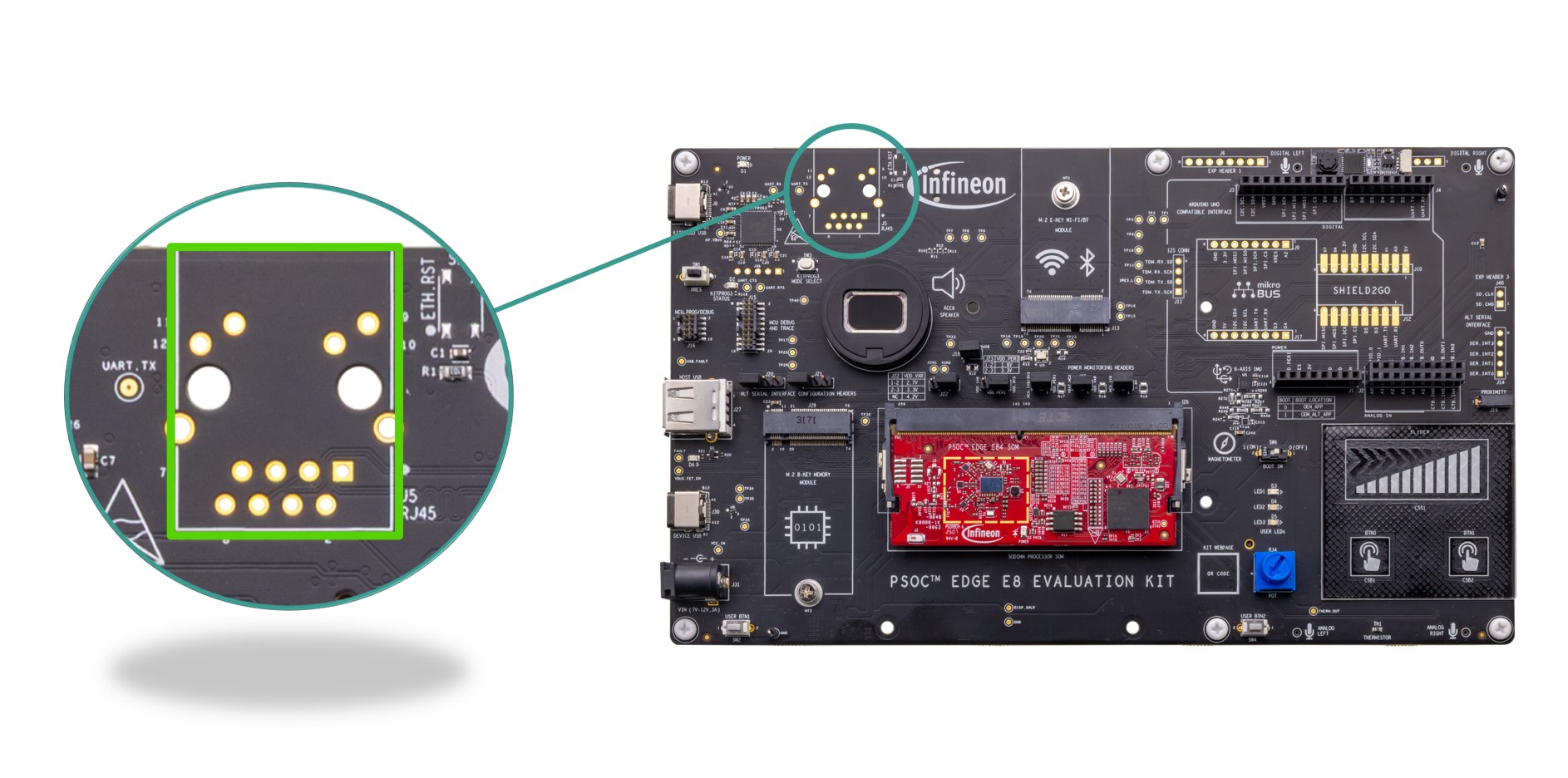
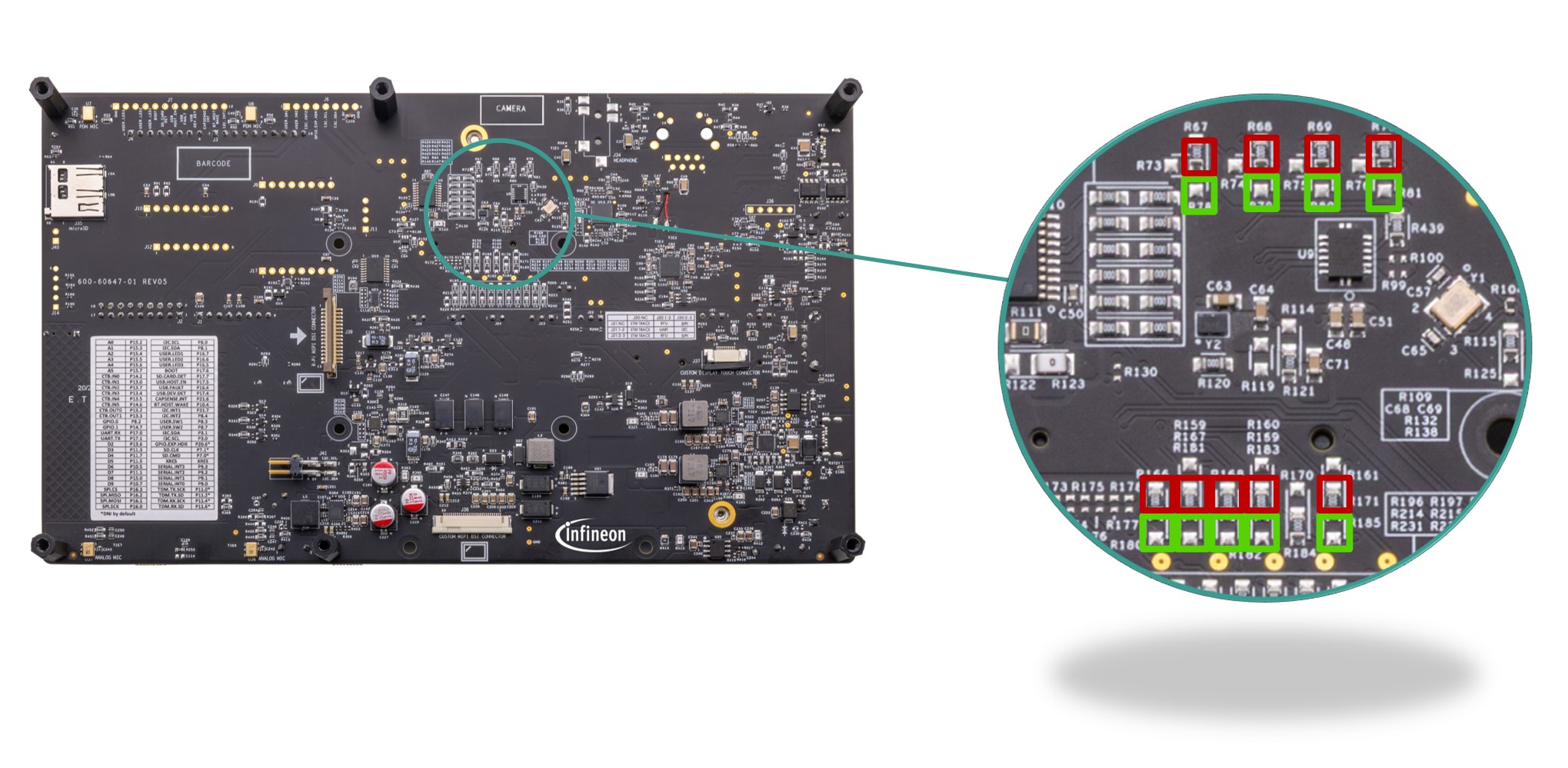
Note:
Removed parts locations are highlighted with red and parts to be mounted are highlighted with green
Rework for RMII mode
Rework instructions for Ethernet RMII mode.
First, perform the rework for MII mode as mentioned in section
Rework for MII mode
. Additionally, do the following rework on the baseboard as follows
Function | Remove | Mount | Purpose | MPN (for mounting) |
|---|---|---|---|---|
Enable RMII signals and configuration | R115, R109 | R149 (4.7K), R106 (10K), R98 (10K), R14 (0Ω), R125 (0Ω), R229 (0Ω) | Completes signal routing and configuration for RMII Ethernet operation. |
|
Figure 92.
Rework region on baseboard for enabling Ethernet RMII mode
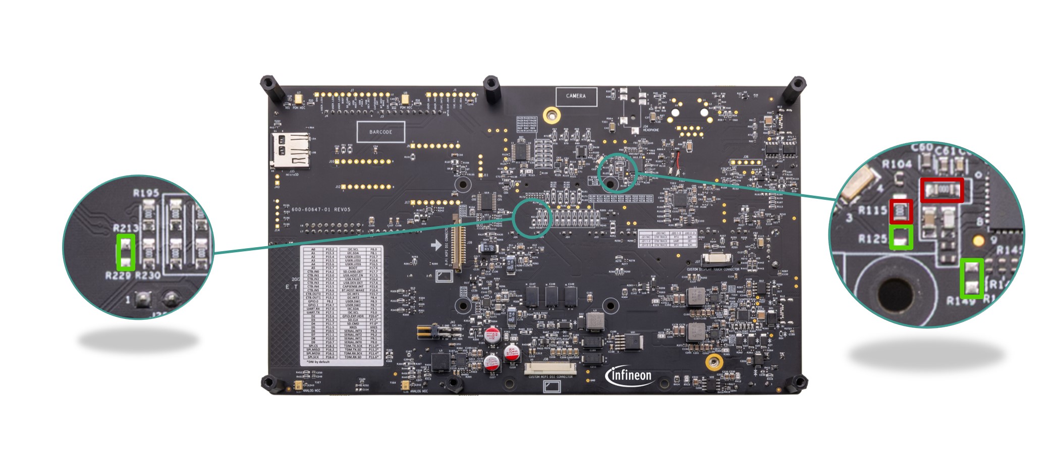
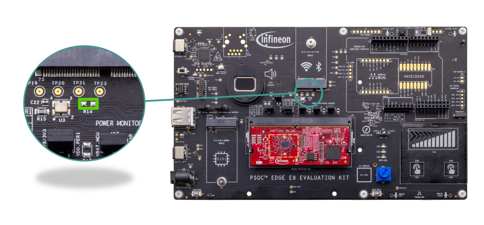
Note:
Removed parts locations are highlighted with red and parts to be mounted are highlighted with green
Rework for KP3 secondary UART interface
Rework instructions for KitProg3 secondary UART Interface.
Perform the following rework on the PSOC™ Edge E8 base board to enable the KitProg3 secondary UART interface.
Function | Remove | Mount | Purpose | MPN (for mounting) |
|---|---|---|---|---|
Enable KitProg3 secondary UART routing | R171, R167, R184, R169 | R161, R159, R170, R160 | Directs UART interface signals to KitProg3 for secondary communication. | 0 Ω resistor, ERJ-3GEY0R00V or equivalent |
Figure 93.
Rework region on baseboard for enabling KP3 secondary UART interface
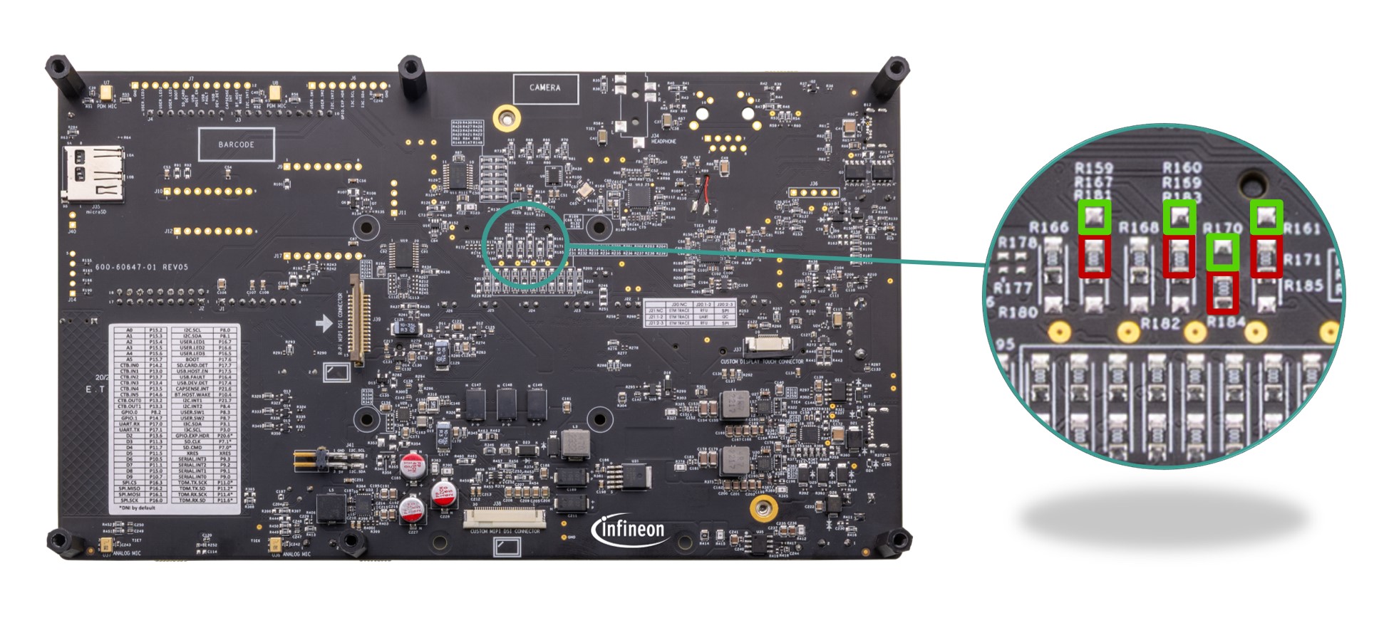
Note:
Removed parts locations are highlighted with red and parts to be mounted are highlighted with green
Rework for Thermistor
Rework instruction for Thermistor.
Perform the following rework on the PSOC™ Edge E8 base board to enable thermistor interface.
Function | Remove | Mount | Purpose | MPN (for mounting) |
|---|---|---|---|---|
Enable thermistor sensing path | R397 | R396 | Connects the thermistor signal path for temperature measurement. | 0 Ω resistor, ERJ-3GEY0R00V or equivalent |
Figure 94.
Rework region on baseboard for enabling Thermistor interface
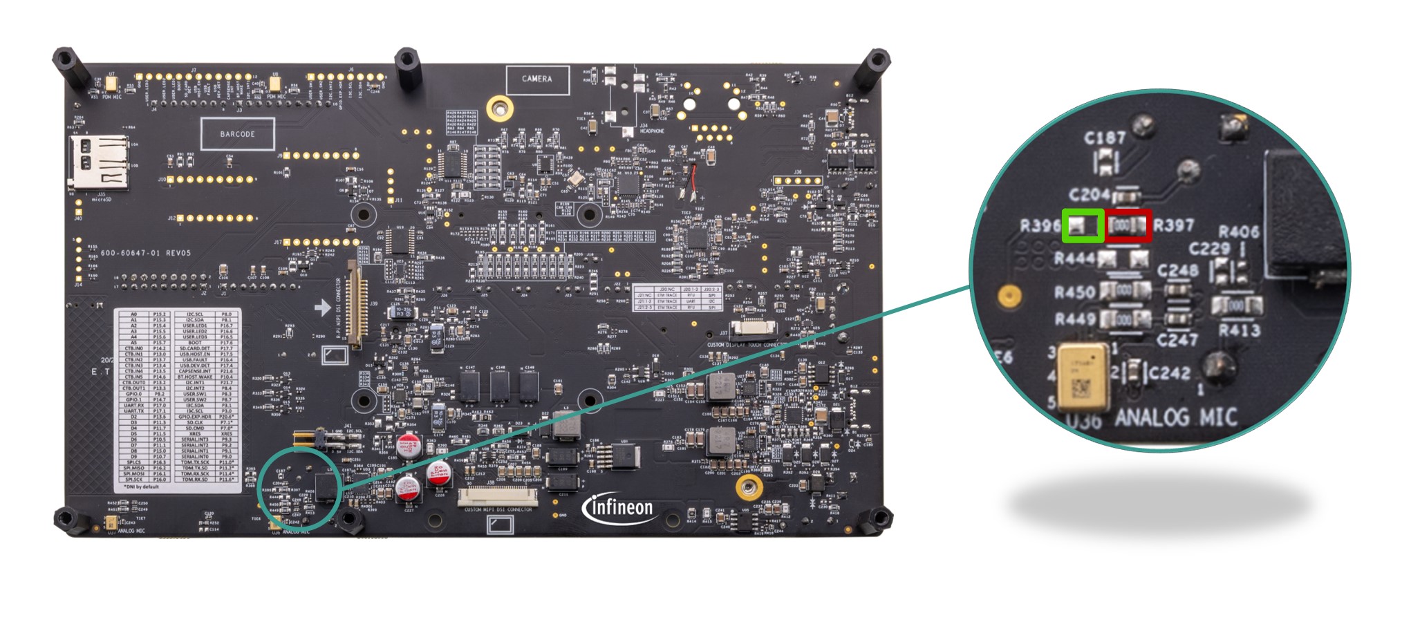
Note:
Removed parts locations are highlighted with red and parts to be mounted are highlighted with green
Rework for bypassing Arduino interface level translator
Rework instructions for bypassing the Arduino interface level translator.
This rework is necessary if level translators (
U19
,
U11
) are not functioning correctly at higher speeds. The following changes allow the Arduino interface to bypass the level translators for direct signal routing on the PSOC™ Edge E8 base board.
Function | Remove | Mount | Purpose | MPN (for mounting) |
|---|---|---|---|---|
Bypass Arduino interface level translators (U19, U11) for direct signal connection | R232, R197, R203, R238, R231, R196, R236, R201, R240, R205, R235, R200, R230, R195, R198, R233, R146, R148, R83, R85 | R215, R221, R214, R219, R223, R218, R213, R216, R147, R84 | Allows Arduino signals to bypass faulty level translators and maintain interface functionality at higher speeds. | 0 Ω resistor, ERJ-3GEY0R00V or equivalent |
Figure 95.
Rework region on baseboard for bypassing Arduino interface level translators
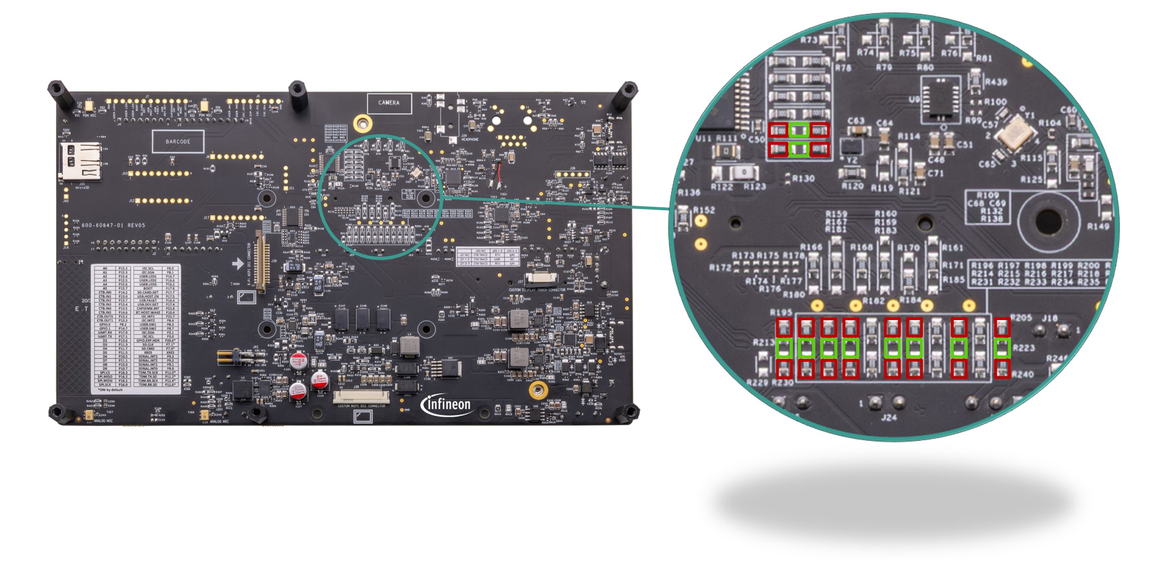
Note:
Removed parts locations are highlighted with red and parts to be mounted are highlighted with green
Rework for bypassing extended I2S interface level translator
Rework instructions for bypassing the extended I2S interface-level translator.
To bypass the extended I2S interface level translator on the PSOC ™Edge E8 base board, perform the following rework actions for direct signal routing.
Function | Remove | Mount | Purpose | MPN (for mounting) |
|---|---|---|---|---|
Bypass extended I2S interface level translator for direct signal connection | R426, R428, R420, R422, R423, R425, R429, R431 | R427, R421, R424, R430 | Enables direct I2S signal routing, bypassing the level translator for improved performance or in case of translator failure. | 0 Ω resistor, ERJ-3GEY0R00V or equivalent |
Figure 96.
Rework region on baseboard for bypassing extended I2S interface level translator
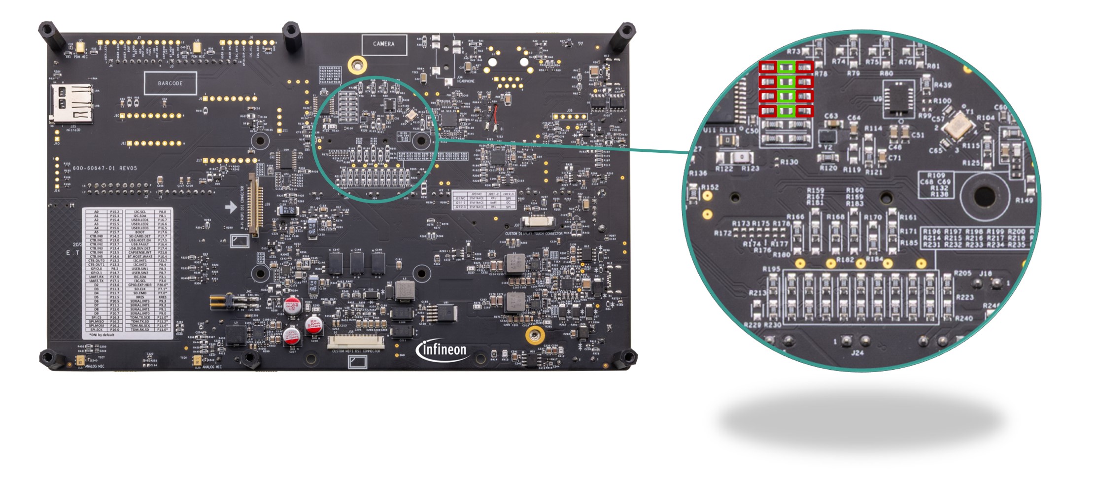
Note:
Removed parts locations are highlighted with red and parts to be mounted are highlighted with green
Rework for expansion headers
Rework for expansion header 1
Rework instructions for expansion header 1.
Perform the following component changes on the PSOC™ Edge E8 base board to configure connections for expansion header 1 as per application needs.
Function | Remove | Mount | Purpose | MPN (for mounting) |
|---|---|---|---|---|
Connect GPIO_EXP_HDR signal to J6.4 | R453 | R454 | Routes P20[6] (GPIO_EXP_HDR) to expansion header pin J6.4. | 0 Ω resistor, Panasonic ERJ-2GE0R00X or equivalent |
Disconnect I2C_INT2 signal from J6.3 | R248 | — | Disconnects P8[4] (I2C_INT2) from expansion header pin J6.3, if not needed. | — |
Disconnect USER_SW2 signal from J6.2 | R413 | — | Disconnects P8[7] (USER_SW2) from expansion header pin J6.2, if not needed. | — |
Disconnect USER_SW1 signal from J6.1 | R416 | — | Disconnects P8[3] (USER_SW1) from expansion header pin J6.1, if not needed. | — |
Provision for expansion header J6 | — | J6 | Populate expansion header for external access to signals via header. | J6: PPPC081LFBN-RC or equivalent |
Figure 97.
Rework region on baseboard for expansion header 1
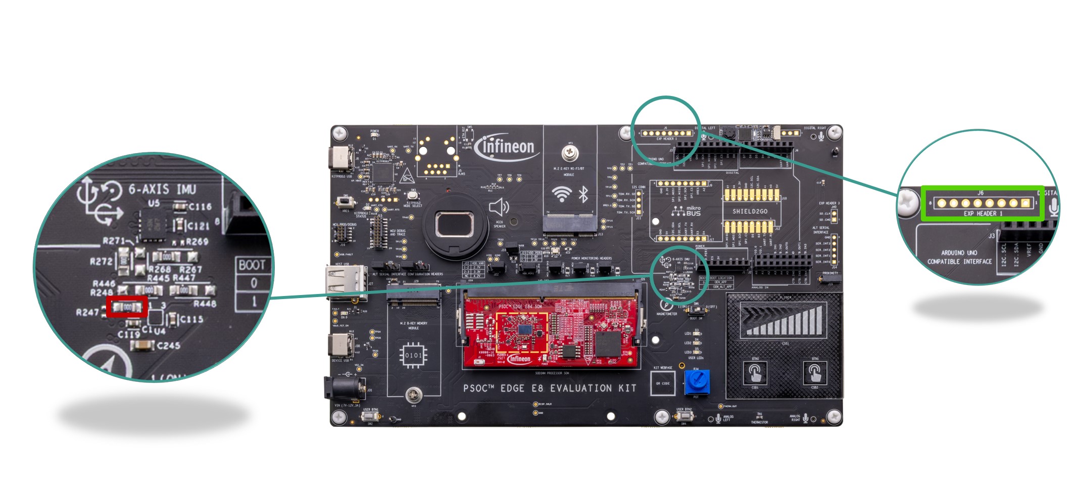
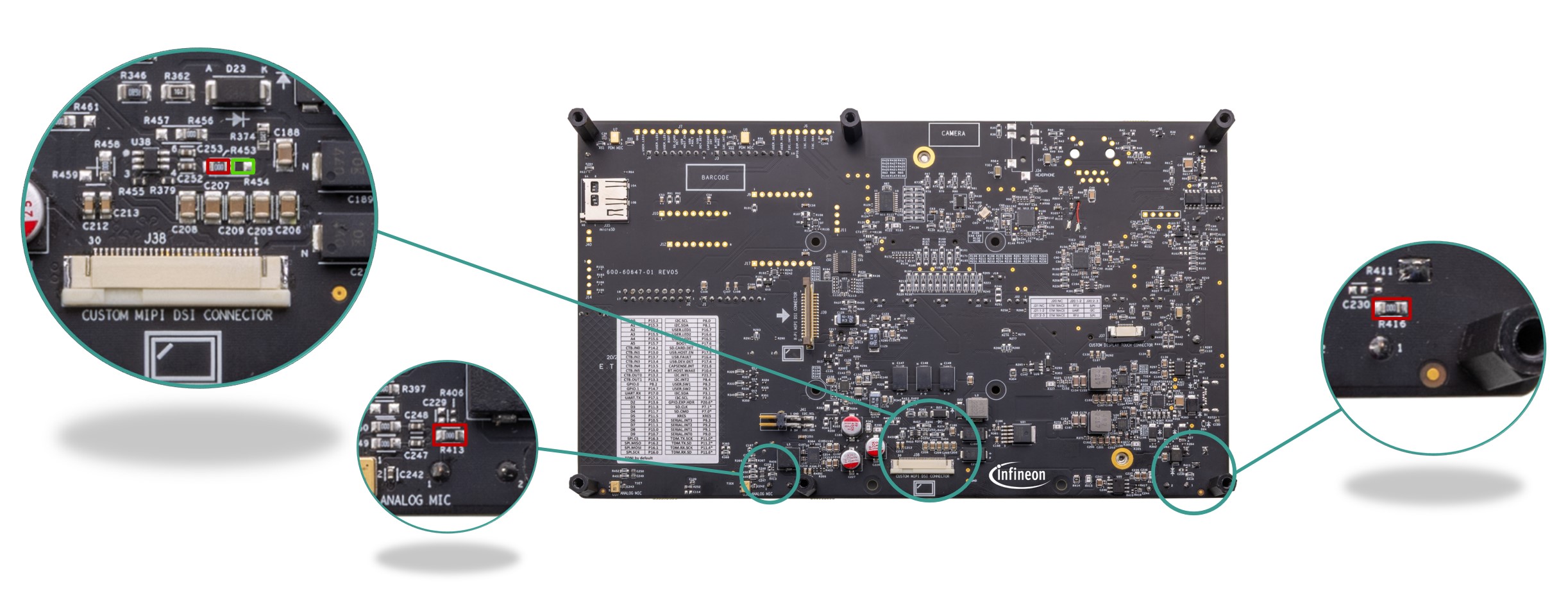
Note:
Removed parts locations are highlighted with red and parts to be mounted are highlighted with green
Rework for expansion header 2
Rework instructions for expansion header 2.
Perform the following component changes on the PSOC™ Edge E84 SOM and PSOC™ Edge E8 base board to configure connections for Expansion Header 2 as per application needs.
Function | Remove | Mount | Purpose | MPN (for mounting) |
|---|---|---|---|---|
Route BT_HOST_WAKE (P10[4]) to J7.11 | R164 | R175 | Connects P10[4] (BT_HOST_WAKE) to expansion header 2, pin J7.11. | 0 Ω resistor, Panasonic ERJ-2GE0R00X or equivalent |
Figure 98.
Rework region on SOM for enabling interface with expansion header 2
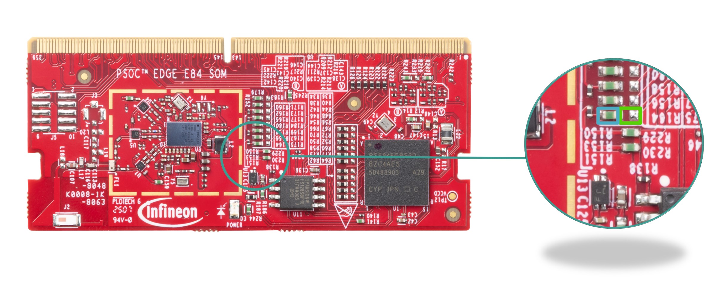
Note:
Removed parts locations are highlighted with blue and parts to be mounted are highlighted with green
Function | Remove | Mount | Purpose | MPN (for mounting) |
|---|---|---|---|---|
Disconnect USER_LED3 from J7.2 | R349 | — | Disconnects P16[5] (USER_LED3) from expansion header pin J7.2, if not needed. | — |
Disconnect USER_LED2 from J7.3 | R333 | — | Disconnects P16[6] (USER_LED2) from expansion header pin J7.3, if not needed. | — |
Disconnect USER_LED1 from J7.4 | R320 | — | Disconnects P16[7] (USER_LED1) from expansion header pin J7.4, if not needed. | — |
Disconnect BOOT from J7.5 | R293 | — | Disconnects P17[6] (BOOT) from expansion header pin J7.5, if not needed. | — |
Disconnect SD_CARD_DET from J7.6 | R284 | — | Disconnects P17[7] (SD_CARD_DET) from expansion header pin J7.6, if not needed. | — |
Disconnect USB_HOST_EN from J7.7 | R289 | — | Disconnects P17[5] (USB_HOST_EN) from expansion header pin J7.7, if not needed. | — |
Disconnect USB_FAULT from J7.8 | R276 | — | Disconnects P16[4] (USB_FAULT) from expansion header pin J7.8, if not needed. | — |
Disconnect USB_DEV_DET from J7.9 | R288 | — | Disconnects P17[4] (USB_DEV_DET) from expansion header pin J7.9, if not needed. | — |
Disconnect BT_HOST_WAKE from J7.11 | R439 | — | Disconnects P10[4] (BT_HOST_WAKE) from expansion header pin J7.11, if not needed. | — |
Disconnect I2C_INT1 from J7.12 | R268 | — | Disconnects P21[7] (I2C_INT1) from expansion header pin J7.12, if not needed. | — |
Provision for expansion header J7 | — | J7 | Populate expansion header for external access to signals via header. | J7: PPPC121LFBN-RC or equivalent |
Figure 99.
Rework region on baseboard for expansion header 2
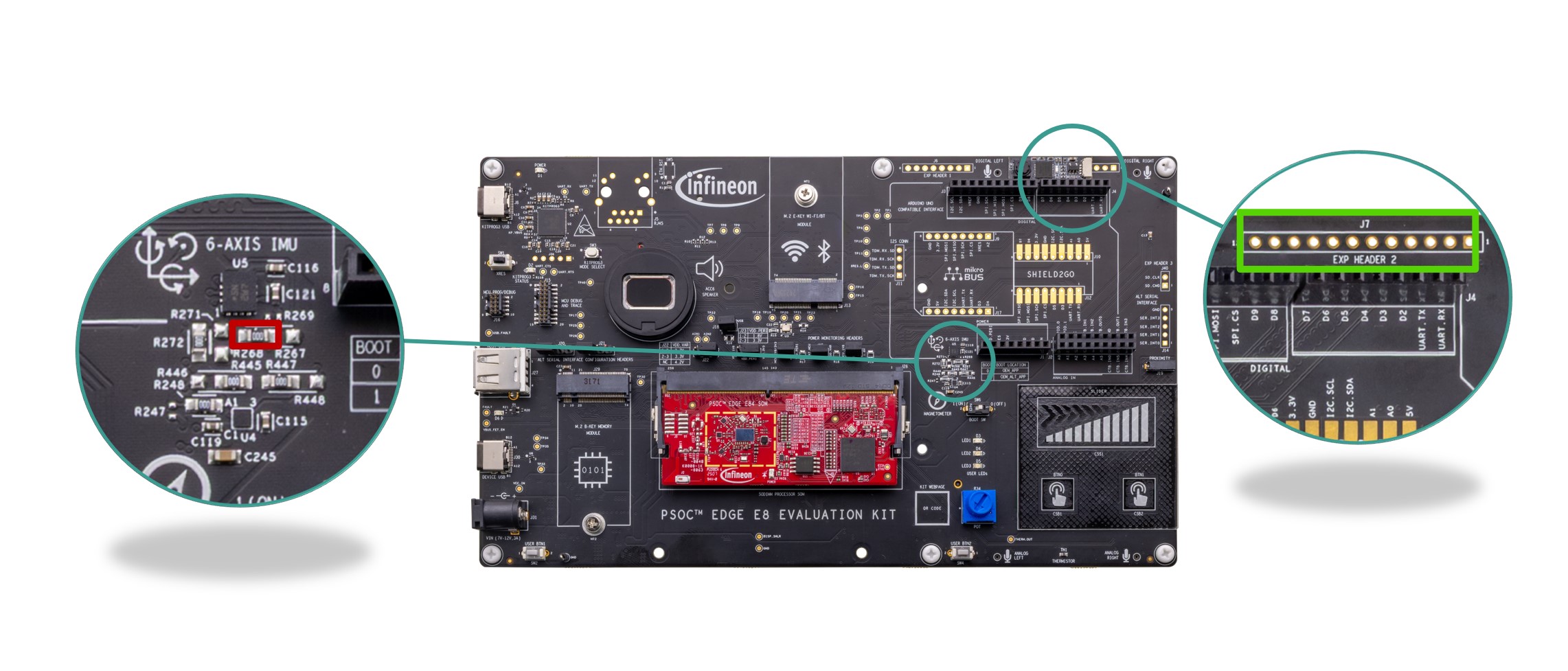
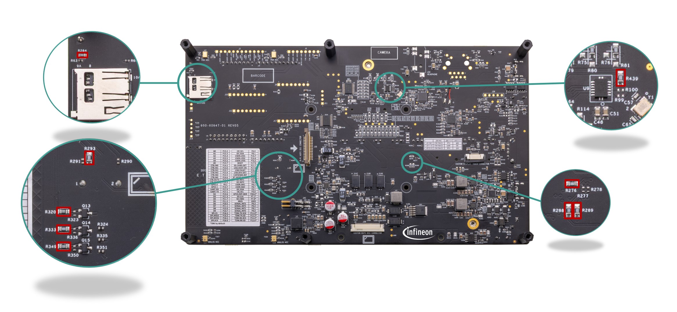
Note:
Removed parts locations are highlighted with red and parts to be mounted are highlighted with green
Rework for expansion header 3
Rework instructions for expansion header 3.
Perform the following rework on the PSOC™ Edge E8 base board to enable Expansion Header 3 signal routing for SD_CMD and SD_CLK as required by your application.
Function | Remove | Mount | Purpose | MPN (for mounting) |
|---|---|---|---|---|
Route SD_CMD (P7[0]) to J40.1 | R435 | R437 | Connects SD_CMD to expansion header 3, pin J40.1. | 0 Ω resistor, ERJ-3GEY0R00V or equivalent |
Route SD_CLK (P7[1]) to J40.2 | R434 | R436 | Connects SD_CLK to expansion header 3, pin J40.2. | 0 Ω resistor, ERJ-3GEY0R00V or equivalent |
Provision for expansion header J40 | — | J40 | Populate expansion header for external access to SD_CMD and SD_CLK signals. | J40: PPPC021LFBN-RC or equivalent |
Figure 100.
Rework region on baseboard for expansion header 3
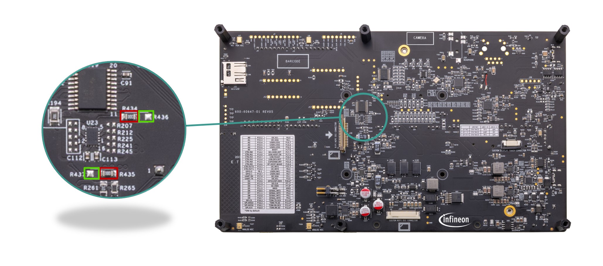
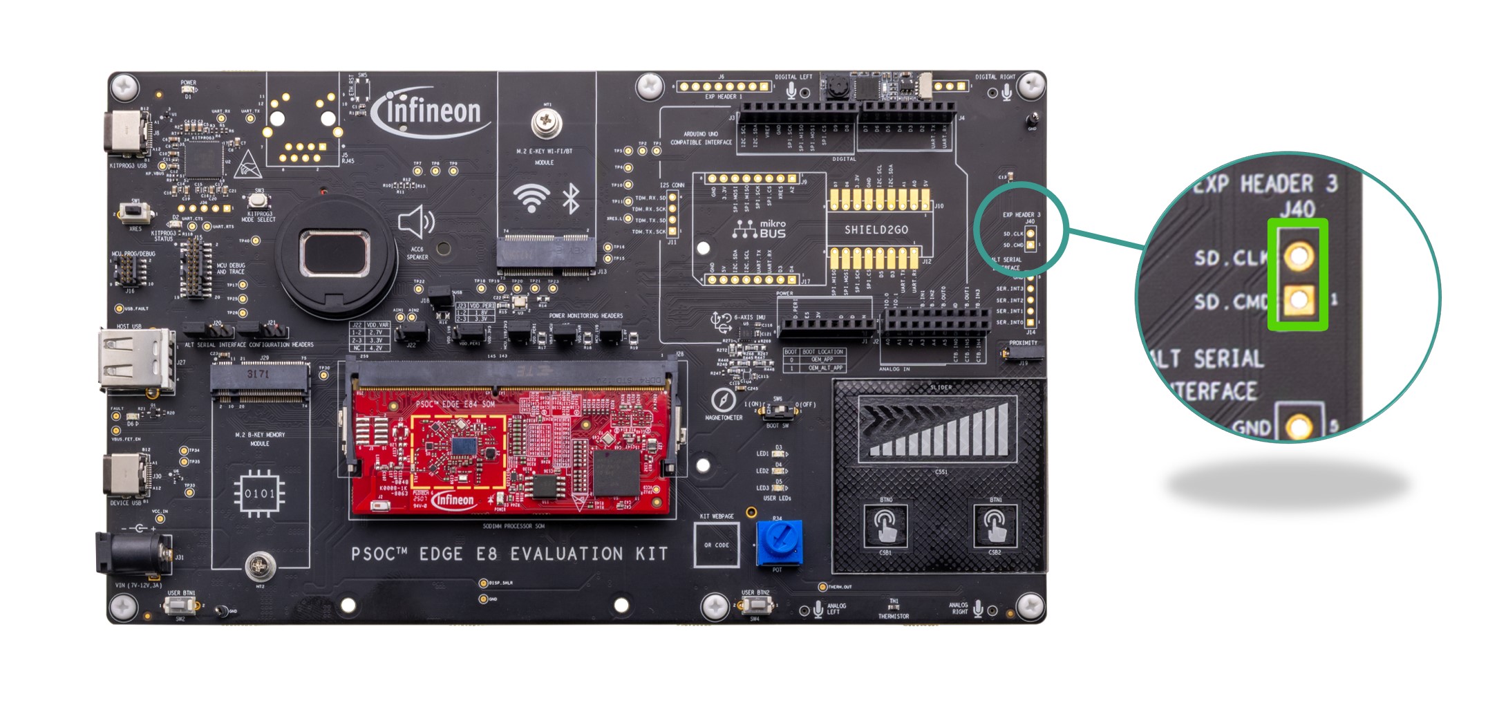
Note:
Removed parts locations are highlighted with red and parts to be mounted are highlighted with green
Rework for extended I2S interface
Rework instructions for the extended I2S interface.
To enable the extended I2S interface on the PSOC™ Edge E8 base board, perform the following component changes for correct signal routing to the external connector.
Function | Remove | Mount | Purpose | MPN (for mounting) |
|---|---|---|---|---|
Route extended I2S signals to external connector | R67, R68, R69, R70 | R73, R74, R75, R76 | Connects extended I2S signals to the external interface for audio applications. | 0 Ω resistor, ERJ-3GEY0R00V or equivalent |
Provision for extended I2S connector | — | J11 | Populates external connector for extended I2S output. | J11: P9401-04-21 or equivalent |
Figure 101.
Rework region on SoM for enabling extended I2S interface
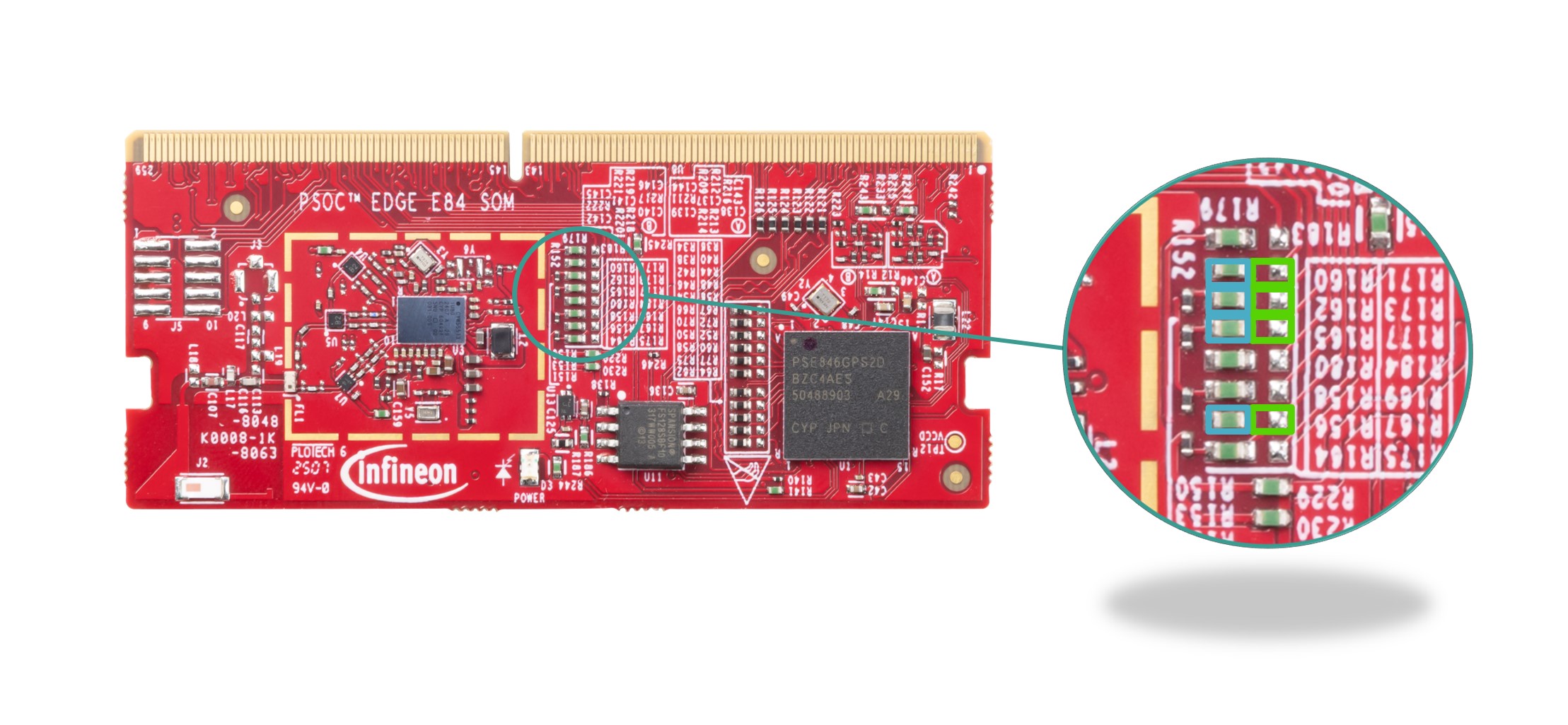
Note:
Removed parts locations are highlighted with blue and parts to be mounted are highlighted with green
Figure 102.
Rework on baseboard for extended I2S interface
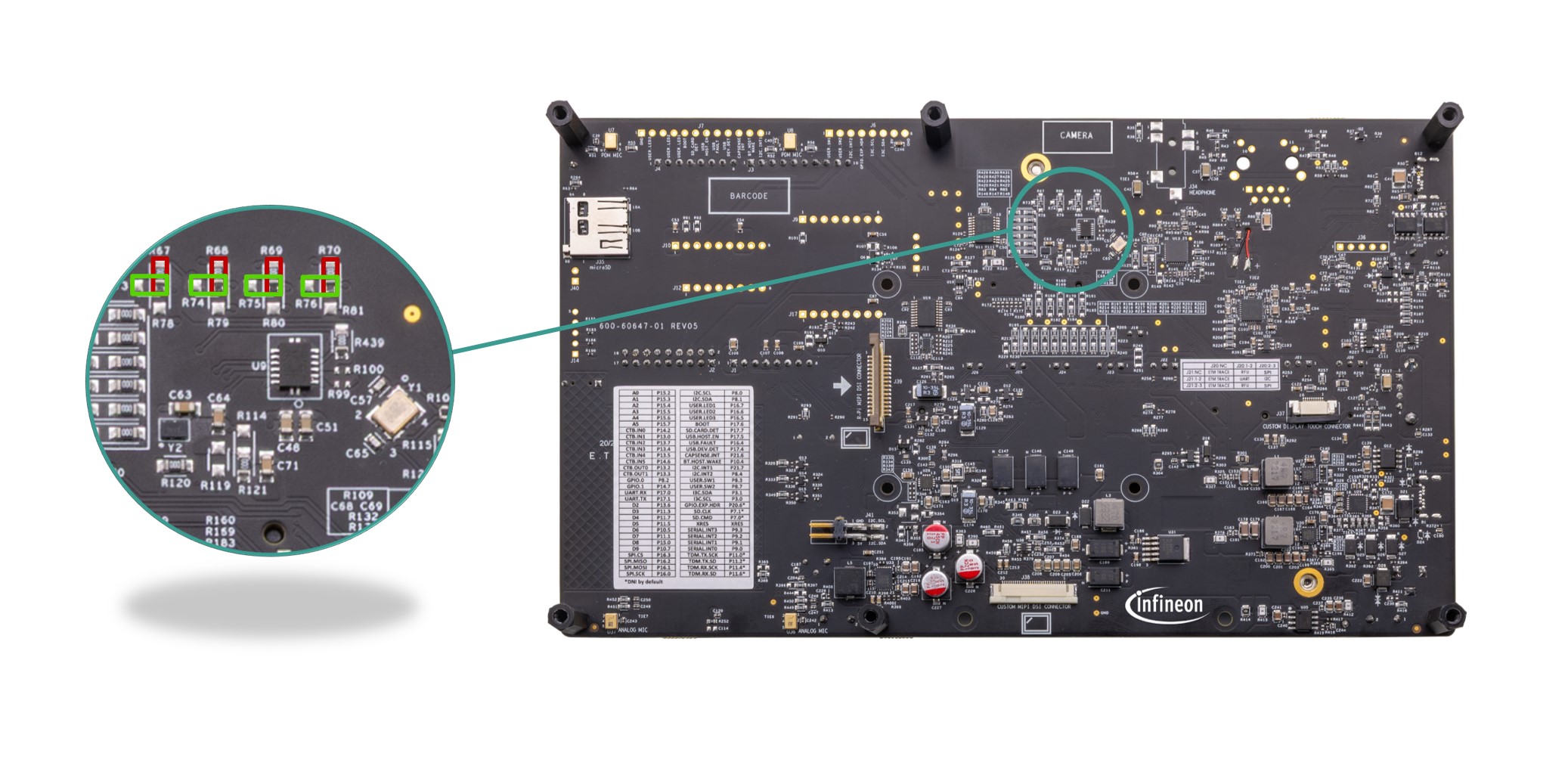
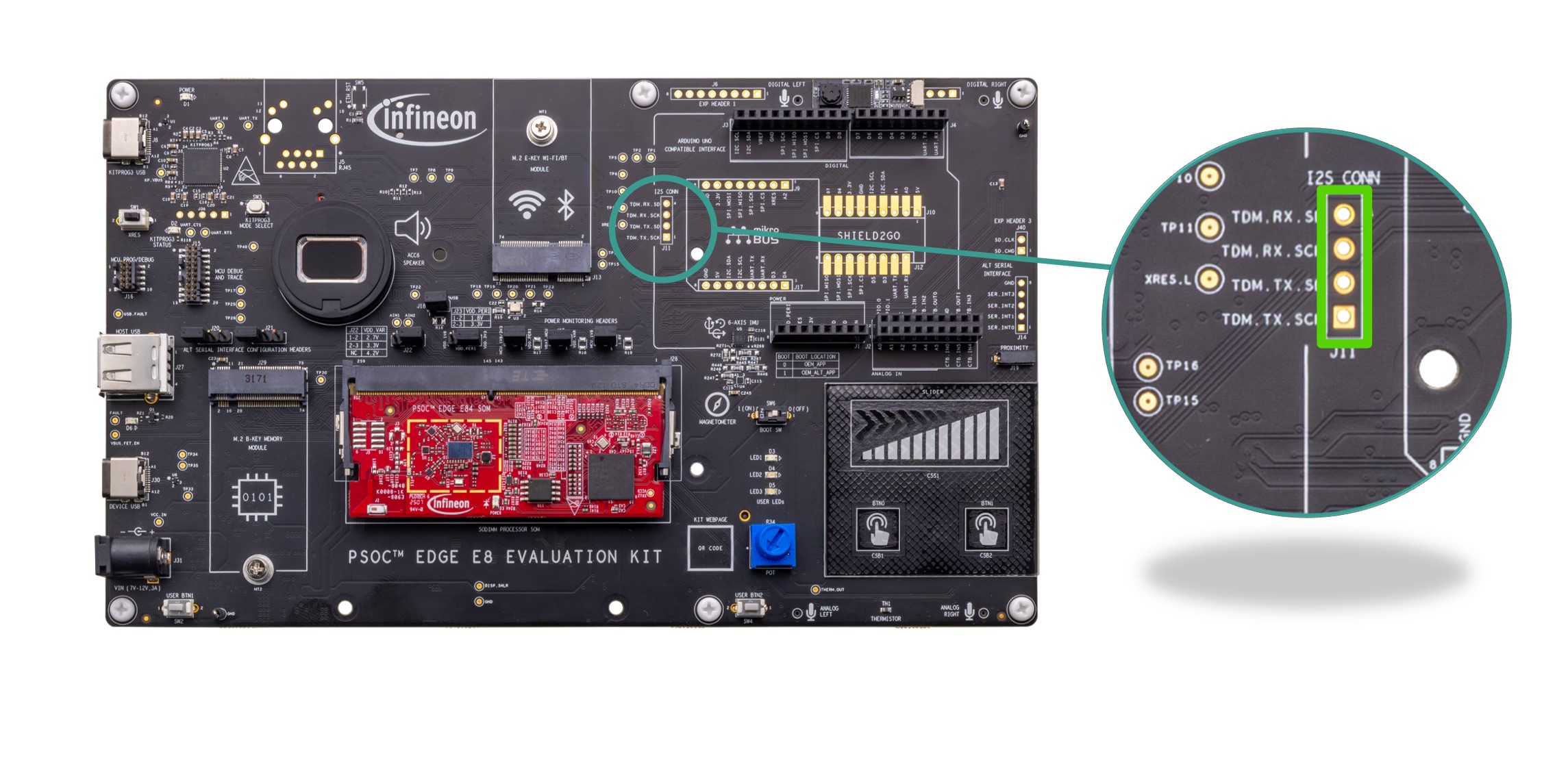
Note:
Removed parts locations are highlighted with red and parts to be mounted are highlighted with green
Rework for MIPI-DSI custom display interface
Rework instructions for the MIPI-DSI custom display interface to support 10.1 inch or 1.43 inch displays.
To support either a 10.1 inch or 1.43 inch custom display with the MIPI-DSI interface on the PSOC™ Edge E8 base board, perform the following rework actions as applicable for your display type.
Function | Remove | Mount | Purpose | MPN (for mounting) |
|---|---|---|---|---|
Configure for 10.1 inch display | R27, R26, R25, R24, R23, R22 | R33, R32, R31, R30, R29, R28 | Routes MIPI-DSI signals optimized for 10.1 inch custom display interface. | 0 Ω resistor, ERJ-3GEY0R00V or equivalent |
Configure for 1.43 inch display (in addition to 10.1 inch rework) | R462 | R463 | Further adapts MIPI-DSI interface for 1.43 inch display requirements. This routes 5V supply for 1.43inch display. | 0 Ω resistor, ERJ-3GEY0R00V or equivalent |
Figure 103.
Rework region on baseboard for MIPI-DSI custom display interface
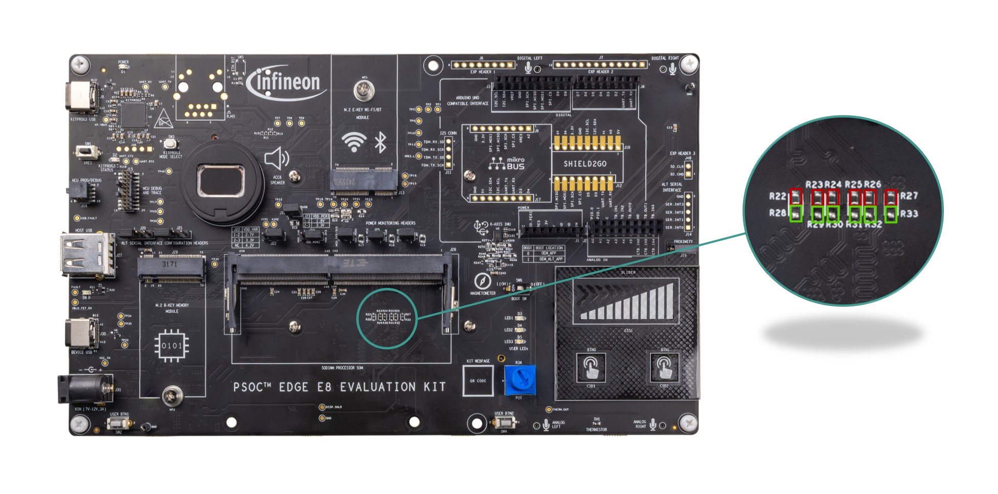
Note:
The rework region is located underneath the SoM
Note:
Removed parts locations are highlighted with red and parts to be mounted are highlighted with green
Figure 104.
Rework region on baseboard for additional rework of 1.43 inch custom display interface
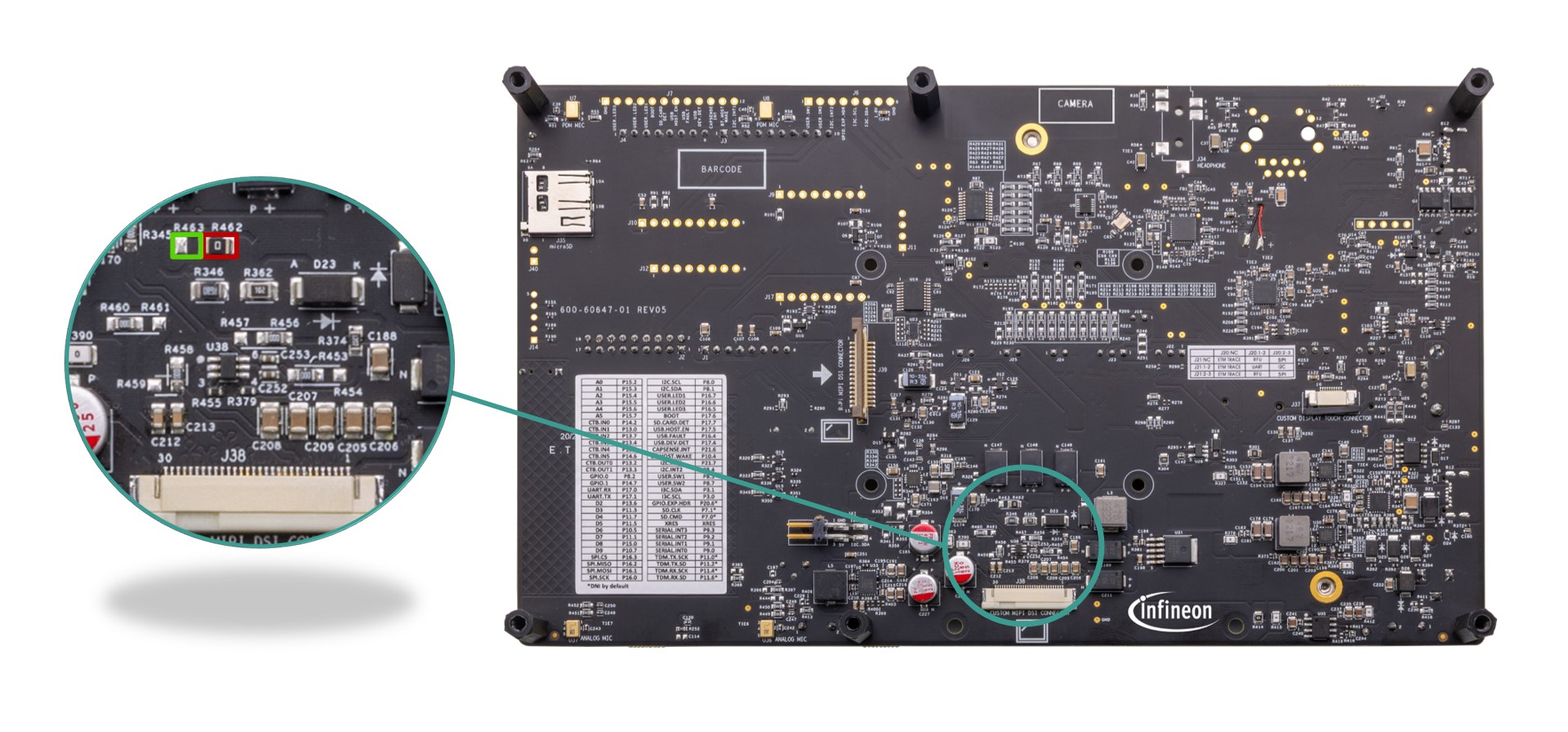
Note:
Removed parts locations are highlighted with red and parts to be mounted are highlighted with green
Rework for Headphone AHJ and OMTP Modes
Rework instructions for Headphone AHJ and OMTP mode.
To configure the PSOC™ Edge E8 base board for either AHJ or OMTP headphone modes, use the following rework instructions. The board is supplied by default in AHJ mode (
R38
mounted,
R35
not mounted). To switch to OMTP mode, remove
R38
and mount
R35
. The headphone connector
J34
must be populated for both modes.
Function | Remove | Mount | Purpose | MPN (for mounting) |
|---|---|---|---|---|
Configure for AHJ headphone mode (default) | R35 | R38, J34 | Sets headphone jack wiring for AHJ/CTIA standard. J34 must be populated for either mode. | R38: 0 Ω resistor, ERJ-3GEY0R00V or equivalent; J34: SJ-43516-SMT-TR or equivalent |
Configure for OMTP headphone mode | R38 | R35, J34 | Sets headphone jack wiring for OMTP standard. J34 must be populated for either mode. | R35: 0 Ω resistor, ERJ-3GEY0R00V or equivalent; J34: SJ-43516-SMT-TR or equivalent |
Figure 105.
Rework on Baseboard for Headphone AHJ mode
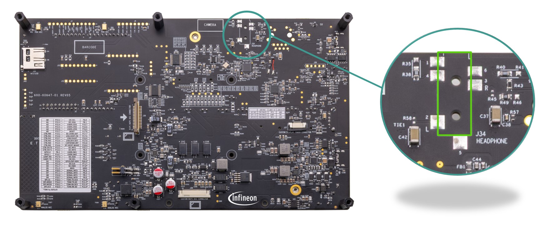
Note:
Removed parts locations are highlighted with red and parts to be mounted are highlighted with green
Figure 106.
Rework on Baseboard for Headphone OMTP mode
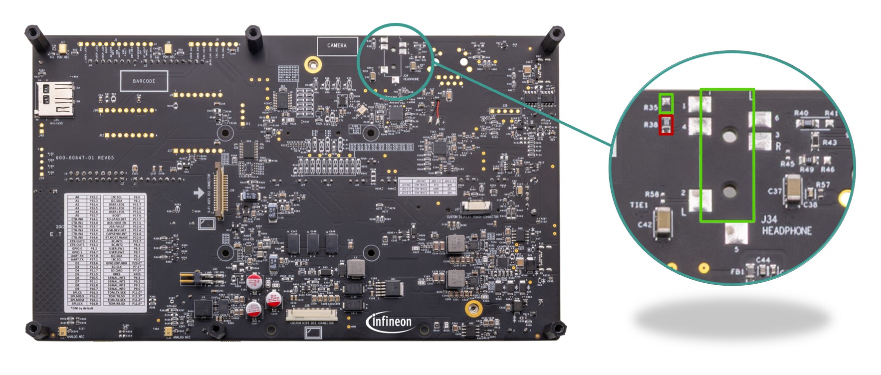
Note:
Removed parts locations are highlighted with red and parts to be mounted are highlighted with green
Rework for CY8CKIT-026 CAN and LIN shield
Rework instructions for CY8CKIT-026 CAN and LIN shield.
To avoid interference from LEDs connected to
J3.4
–
J3.6
on the CY8CKIT-026 CAN and LIN shield, and to route CAN/LIN I/Os to a secondary header (
J4.6
–
J4.8
) on the PSOC™ Edge E8 base board, perform the following rework.
Note:
Arduino compatible shields will not function after this modification
Function | Remove | Mount | Purpose | MPN (for mounting) |
|---|---|---|---|---|
Route CAN/LIN I/Os from J3.4–J3.6 to J4.6–J4.8, removing LED interference | R237, R202, R204, R239, R199, R234 | R220, R222, R217 | Redirects CAN/LIN I/Os to alternate pins for shield compatibility, disables default Arduino functionality. | 0 Ω resistor, ERJ-3GEY0R00V or equivalent |
Figure 107.
Rework region on baseboard for CY8CKIT-026 CAN and LIN shield
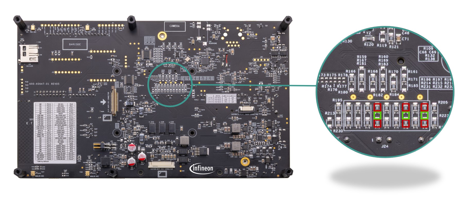
Note:
Removed parts locations are highlighted with red and parts to be mounted are highlighted with green
Rework for JTAG interface using external programmer/debugger
Rework instructions for the JTAG interface using external programmer/debugger.
To enable programming or debugging via an external JTAG programmer through the 10-pin SWD/JTAG (
J16
) or 20-pin ETM/TRACE (
J15
) header on the PSOC™ Edge E8 base board, perform the following rework.
Note:
The on board KitProg3 JTAG functionality will not be available after this modification.
Function | Remove | Mount | Purpose | MPN (for mounting) |
|---|---|---|---|---|
Enable external JTAG programming/debugging via headers J16 (SWD/JTAG) or J15 (ETM/TRACE) | R187 | — | Isolates on board KitProg3 JTAG circuit and allows external debug/program access. | — |
Figure 108.
Rework region on baseboard for enabling JTAG interface using external programmer/debugger
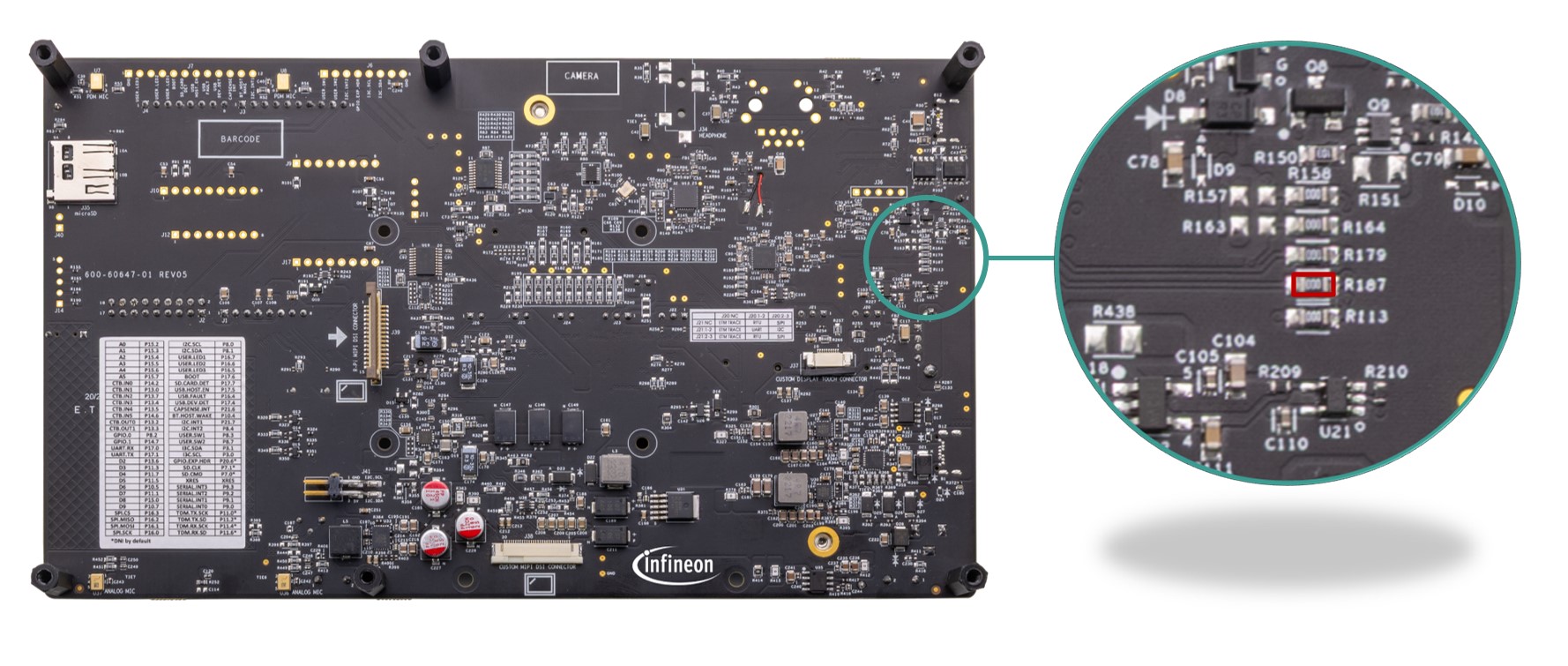
Note:
Removed parts locations are highlighted with red
Rework for PSOC™ Edge E84 MCU low power current measurement
Rework instructions for MCU low power current measurement
To enable low power current measurement for the PSOC™ Edge E84 MCU, perform the following rework steps on the SoM.
Function | Remove | Mount | Purpose | MPN (for mounting) |
|---|---|---|---|---|
Prepare MCU for low power current measurement | R229, R230, R247 | — | Isolates supply for pull up resistors of various interfaces to allow accurate low power current measurement of the MCU. | — |
Figure 109.
Rework on PSOC™ Edge E84 SOM
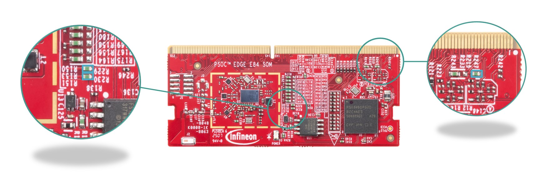
Note:
Removed parts locations are highlighted with blue
Function | Remove | Mount | Purpose | MPN (for mounting) |
|---|---|---|---|---|
Prepare MCU for low power current measurement | R187, R397 | — | Isolates supply and current paths to allow accurate low power current measurement of the MCU. | — |
Figure 110.
Rework region on PSOC™ Edge E8 base board
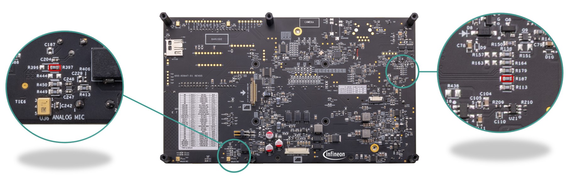
Note:
Removed parts locations are highlighted with red.
Note:
These reworks will impact the functionality of WIFI/BT, Analog microphone interface, on-board KitProg3 JTAG interface and potentiometer interface.
Bill of materials
See the bill of materials available on the
kit webpage.
Frequently asked questions
I don’t have a Type-C connector on my PC. Can I still connect and use this kit?
Partially yes. To evaluate the basic PSOC™ Edge E84 MCU features without the display applications, any PC with USB2.0 connectivity is sufficient. To evaluate the display applications, an additional DC power adapter or a Type-C power adapter with minimum 9 V, 3 A can be used to power the board through
J31
or
J30
connector along with the KitProg3 USB (
J8
). See
Power inputs and over-voltage protection
section for more details
How can I access Smart I/O and other GPIOs connected to the MCU?
All the unused or multiplexed IOs are brought out to the Arduino compatible headers (
J1
-
J4
), Expansion headers (
J6
,
J7
,
J40
) and Extended I2S interface header (
J11
) which can be accessed. See section
I/O headers
for more details
What can I use the U.FL connector for and what is the typical mating cycle for these connectors?
U.FL can be used for conductive measurements and to connect external antenna. U.FL connectors are not designed for reconnection. They are rated only for approximately 30 mating cycles
What are the jumpers on board for?
There are total 8 jumpers on the board:
4 jumpers for MCU power monitoring:
J18
(VDDUSB_3V3),
J24
(VDD/VDDIO_1V8_3V3),
J25
(VBAT_MCU),
J26
(VDD/VDDIO_1V8). See section
PSOC™ Edge E84 power selection and current monitoring headers
for more details
2 jumpers for power selection:
J22
(VDD_VAR),
J23
(VDD_PERI). See sections
PSOC™ Edge E84 power selection and current monitoring headers
and
Voltage regulators
for more details
2 jumpers for Alternate serial interface configuration:
J20
,
J21
. See section
Alternative serial interface
for more details
I am not getting datasheet Deep sleep power numbers on EVK
Back power and or leakage on the PSOC™ Edge E8 base board and PSOC™ Edge E84 SOM might lead to skewed Deep Sleep power numbers. Remove resistors
R187
and
R397
on the PSOC™ Edge E8 base board, and
R229
,
R230
, and
R247
on the PSOC™ Edge E84 SOM, as mentioned in the
Rework for PSOC™ Edge E84 MCU low power current measurement
section in the kit guide to avoid this leakage path to on board peripherals
What are the input voltage levels on the board?
Table 58.
Input voltage levels are as follows:
Supply
Typical i/p voltage
Absolute maximum
KitProg3 Type-C USB (
J8
)
5 V
5.5 V
Device USB Type-C (
J30
)
5 V to 15 V
17 V
VIN connector (
J31
/
J1.1
)
7 V to 12 V
12.6 V
Does the kit get powered when I power the kit from another Infineon kit through the J1 header?
Yes, VIN pin on J1 header is the supply input/output pin and can take up to 12 V. See
Power inputs and over-voltage protection
section for more details
With what type of shield from Infineon can I use this board?
See the sections
Table 15
and
Table 16
for the list of supported shields
Can I power PSOC™ Edge E84 MCU using only external programmer at 1.8 V through the J15 or J16 header?
No by default. There is a reverse voltage protection circuit that prevents the board to get powered from any external programmer. Though there is a provision to power the board by bypassing the protection circuit by populating the resistor
R151
, but it is not recommended as it may damage the board or the external programmer in case of any power requirement violations. See section
10-pin SWD/JTAG header
for more details
Glossary
ADC | Analog-to-Digital Converter |
BCR | Barrel Connector Replacement |
BOM | Bill of Materials |
CINT | Integration Capacitor |
CMOD | Modulator Capacitor |
CPU | Central Processing Unit |
CSD | CAPSENSE™ Sigma Delta |
CSX | CAPSENSE™ Crosspoint |
CTANK | Shield Tank Capacitor |
CTS | Clear To Send |
DAC | Digital to Analog Conversion |
DC | Direct Current |
DDR | Double Data Rate |
DSI | Display Serial Interface |
ECO | External Crystal Oscillator |
ESD | Electrostatic Discharge |
ETM | Embedded Trace Macrocell |
EVK | Evaluation Kit |
FET | Field Effect Transistor |
GPIO | General-Purpose Input/Output |
IC | Integrated Circuit |
IDE | Integrated Development Environment |
IMU | Inertial Measurement Unit |
I/O | Input/Output |
IOT | Internet of Things |
I2C | Inter-integrated Circuit |
I2S | Inter-IC Sound |
I3C | Improved Inter-Integrated Circuit |
JTAG | Joint Test Action Group |
LED | Light-emitting Diode |
LPO | Low Power Oscillator |
MCU | Microcontroller Unit |
MEMS | Micro Electro Mechanical systems |
MII | Media-Independent interface |
MIPI | Mobile Industry Processor Interface |
NTC | Negative Temperature Coefficient |
OSPI | Octal Serial Peripheral Interface |
OVP | Overvoltage Protection |
PC | Personal Computer |
PD | Power Delivery |
PDL | Peripheral Driver Library |
PDM | Pulse Density Modulation |
PHY | Ethernet PHY |
PSOC™ | Programmable System-on-Chip |
PMU | Power Management Unit |
QSPI | Quad Serial Peripheral Interface |
RAM | Random Access Memory |
RC | Resistor Capacitor |
RTS | Ready To Send |
RMII | Reduced Media-Independent Interface |
RX | Receiver |
SCL | Serial Clock |
SD | SD card |
SDA | Serial Data |
SDHC | Secure Digital Host Controller |
SDIO | Secure Digital Input Output |
SDK | Software Development Kit |
SMIF | Serial Memory Interface |
SNR | Signal-to-Noise Ratio |
SODIMM | Small Outline Dual In-line Memory Module |
SOM | System On Module |
SPI | Serial Peripheral Interface |
SWCLK | Serial Wire Clock |
SWD | Serial Wire Debug |
SWDIO | Serial Wire Debug Input Output |
SWO | Serial Wire Out |
SRAM | Static Random-Access Memory |
TX | Transmitter |
UART | Universal Asynchronous Receiver Transmitter |
USB | Universal Serial Bus |
WCO | Watch Crystal Oscillator |
WLAN | Wireless LAN |
R-Pi | Raspberry Pi |
XRES | External Reset |
Revision history
Document revision | Date | Description of changes |
|---|---|---|
*B | 2025-09-10 | Release to web |
Trademarks
The Bluetooth® word mark and logos are registered trademarks owned by Bluetooth SIG, Inc., and any use of such marks by Infineon is under license.
PSOC™, formerly known as PSoC™, is a trademark of Infineon Technologies. Any references to PSoC™ in this document or others shall be deemed to refer to PSOC™.
1
Component at the bottom side of the baseboard
2
Component at the bottom side of the SoM
3
Footprint only, not populated on the board
4
Note that for VDD_VAR = 4.2 V, it is required to power the board from the device Type-C USB connector (
J30
) with minimum 9 V or VIN header (
J31
)/Arduino header (
J1.1
) with minimum 7 V to meet the minimum input voltage requirement of the regulator for proper operation.
6
May support any other R-Pi-compatible display that complies with the standard 15-pin R-Pi pin out.
7
J41 is only for displays that supports I2C touch interface
8
Not connected to MCU by default