KIT_PSE84_AI PSOC™ Edge E84 AI Kit guide
About this document
Important notice
“Evaluation Boards and Reference Boards” shall mean
products embedded on a printed circuit board (PCB) for demonstration and/or
evaluation purposes, which include, without limitation, demonstration, reference
and evaluation boards, kits and design (collectively referred to as “Reference
Board”).
Environmental conditions have been considered in
the design of the Evaluation Boards and Reference Boards provided by Infineon
Technologies. The design of the Evaluation Boards and Reference Boards has been
tested by Infineon Technologies only as described in this document. The design
is not qualified in terms of safety requirements, manufacturing and operation
over the entire operating temperature range or lifetime.
The Evaluation Boards and Reference Boards provided
by Infineon Technologies are subject to functional testing only under typical
load conditions. Evaluation Boards and Reference Boards are not subject to the
same procedures as regular products regarding returned material analysis (RMA),
process change notification (PCN) and product discontinuation (PD).
Evaluation Boards and Reference Boards are not
commercialized products, and are solely intended for evaluation and testing
purposes. In particular, they shall not be used for reliability testing or
production. The Evaluation Boards and Reference Boards may therefore not comply
with CE or similar standards (including but not limited to the EMC Directive
2004/EC/108 and the EMC Act) and may not fulfill other requirements of the
country in which they are operated by the customer. The customer shall ensure
that all Evaluation Boards and Reference Boards will be handled in a way which
is compliant with the relevant requirements and standards of the country in
which they are operated.
The Evaluation Boards and Reference Boards as well
as the information provided in this document are addressed only to qualified and
skilled technical staff, for laboratory usage, and shall be used and managed
according to the terms and conditions set forth in this document and in other
related documentation supplied with the respective Evaluation Board or Reference
Board.
It is the responsibility of the customer’s
technical departments to evaluate the suitability of the Evaluation Boards and
Reference Boards for the intended application, and to evaluate the completeness
and correctness of the information provided in this document with respect to
such application.
The customer is obliged to ensure that the use of
the Evaluation Boards and Reference Boards does not cause any harm to persons or
third party property.
The Evaluation Boards and Reference Boards and any
information in this document is provided "as is" and Infineon Technologies
disclaims any warranties, express or implied, including but not limited to
warranties of non-infringement of third party rights and implied warranties of
fitness for any purpose, or for merchantability.
Infineon Technologies shall not be responsible for
any damages resulting from the use of the Evaluation Boards and Reference Boards
and/or from any information provided in this document. The customer is obliged
to defend, indemnify and hold Infineon Technologies harmless from and against
any claims or damages arising out of or resulting from any use thereof.
Infineon Technologies reserves the right to modify
this document and/or any information provided herein at any time without further
notice.
Safety precautions
Note:
Please note the following warnings regarding the hazards associated with development systems.
 | Caution: The evaluation or reference board contains parts and
assemblies sensitive to electrostatic discharge (ESD).
Electrostatic control precautions are required when
installing, testing, servicing or repairing the assembly.
Component damage may result if ESD control procedures are
not followed. If you are not familiar with electrostatic
control procedures, refer to the applicable ESD protection
handbooks and guidelines. |
Introduction
The PSOC™ Edge E84 AI kit enables you to evaluate and develop your applications using the PSOC™ Edge E84 series MCU (called “PSOC™ E84”) and a multitude of on-board multimedia, Machine Learning (ML), and connectivity features like Raspberry Pi compatible MIPI-DSI displays, analog and digital microphones for audio interfaces, and AIROC™ CYW55513IUBGT based Wi-Fi & Bluetooth® combo Murata Type 2FY (LBEE5HY2FY) connectivity module. The kit also has 512-Mbit Quad-SPI NOR Flash and 128-Mbit Octal-SPI HYPERRAM™. The board features an on-board programmer/debugger (KitProg3), JTAG/SWD debug headers, expansion I/O header, USB-C connectors, 6-axis IMU sensor, 3-axis magnetometer, barometric pressure sensor, humidity sensor, RADAR sensor, user LEDs and user button. The MCU power domain and peripheral power domain supports following operating voltages - 1.8V and 3.3V.
PSOC™ E84 MCU is an ultra-low-power PSOC™ device specifically designed for ML, wearables and IoT products like smart thermostats, smart locks, smart home appliances and industrial HMI.
PSOC™ E84 MCU is a true programmable embedded system-on-chip with dual CPUs, integrating a 400 MHz Arm® Cortex® -M55 as the primary application processor, a 200 MHz Arm® Cortex® -M33 that supports low-power operations, and a 400 MHz Arm® Ethos-U55 as a neural net companion processor, graphics and audio block, DSP capability, security enclave with crypto accelerators and protection units, high-performance memory expansion capability (QSPI, and Octal HYPERRAM™), low-power analog subsystem with high performance analog-to-digital conversion and low-power comparators, on-board IoT connectivity module , communication channels, programmable analog and digital blocks that allow higher flexibility, in-field tuning of the design, and faster time-to-market.
You can use ModusToolbox™ software to develop and debug your PSOC™ E84 MCU projects.
ModusToolbox™ software
is a set of tools that enable you to integrate these devices into your existing development methodology.
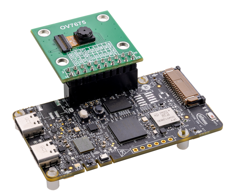
Kit contents
PSOC™ Edge E84 AI Kit includes:
PSOC™ Edge E84 AI board
OV7675 DVP camera module
Figure 1.
Kit content
Getting started
This guide will help you get acquainted with this evaluation kit:
The Kit operation chapter describes the major features of the PSOC™ Edge E84 AI board and its functionalities, such as programming and debugging
The Hardware chapter provides a detailed hardware description, kit schematics, and the bill of materials (BOM)
Application development using PSOC™ Edge E84 AI kit is supported in ModusToolbox™ software. For the latest software support for this development kit, including the different development ecosystems, see the AN235935 - Getting started with PSOC™ Edge E84 MCU on ModusToolbox™ software.
ModusToolbox™ software is a free development ecosystem that includes the ModusToolbox™ IDE. Using ModusToolbox™ IDE, you can enable and configure device resources, middleware libraries, program and debug the device. You can download the software from the
ModusToolbox™ home page
DEEPCRAFT™ Studio is a development platform for machine learning on edge devices. Its work flow is optimized for embedded devices
There are various Code Examples to evaluate the PSOC™ Edge E84 AI kit, which familiarizes you with PSOC™ Edge E84 MCU and helps you creates your own design. These examples can be accessed through ModusToolbox™ Project Creator tool. Alternatively, you can visit Code examples for ModusToolbox™ software page to access these examples
Board details
The PSOC™ Edge E84 AI board has the following features:
PSOC™ Edge E84 MCU - PSE846GPS2DBZC4A.See the device
datasheet
AIROC™
CYW55513IUBGT
based Wi-Fi & Bluetooth® combo Murata Type 2FY (
LBEE5HY2FY
) connectivity module
Raspberry Pi compatible MIPI-DSI display interface
512-Mbit external Quad-SPI NOR flash that provides fast, expandable memory for data and code
128-Mbit PSRAM
6-axis accelerometer and gyroscope (BMI270), 3-axis magnetometer (BMM350), XENSIV™ digital barometric pressure sensor with built-in temperature sensor (DPS368), digital humidity and temperature sensor (SHT40) and XENSIV™ 60 GHz RADAR sensor (BGT60TR13C) for data collection
KitProg3 onboard SWD programmer/debugger, USB-UART, and USB-I2C bridge functionality
Supports 1.8 V and 3.3 V operation of PSOC™ Edge E84 MCU
Three user LEDs, a user button, and a reset button for PSOC™ Edge E84 MCU
One mode selection button and one status LED for KitProg3
The following figure shows the pinout of the evaluation board.
Figure 2.
Board pinout
PSOC™ Edge E84 MCU pin number | Connection signal | Functionality |
|---|---|---|
XRES | Hardware Reset | Used to reset the PSOC™ Edge E84 MCU |
P0.0 | Memory reset | Resets the connected external memory |
P0.1 | PSRAM _CS | Chip select signal for the PSRAM module |
P1.0 | QSPI FLASH DATA0 | Data line 0 for QSPI Flash interface |
P1.1 | QSPI FLASH DATA1 | Data line 1 for QSPI Flash interface |
P1.2 | QSPI FLASH DATA2 | Data line 2 for QSPI Flash interface |
P1.3 | QSPI FLASH DATA3 | Data line 3 for QSPI Flash interface |
P2.0 | QSPI _CS | Chip select signal for QSPI Flash interface |
P3.0 | I3C_SCL | Clock signal for I3C communication |
P3.1 | I3C_SDA | Data signal for I3C communication |
P4.0 | PSRAM DATA0 | Data line 0 for PSRAM interface |
P4.1 | PSRAM DATA1 | Data line 1 for PSRAM interface |
P4.2 | PSRAM DATA2 | Data line 2 for PSRAM interface |
P4.3 | PSRAM DATA3 | Data line 3 for PSRAM interface |
P4.4 | PSRAM DATA4 | Data line 4 for PSRAM interface |
P4.5 | PSRAM DATA5 | Data line 5 for PSRAM interface |
P4.6 | PSRAM DATA6 | Data line 6 for PSRAM interface |
P4.7 | PSRAM DATA7 | Data line 7 for PSRAM interface |
P6.0 | PSOC™ Edge E84 MCU JTAG TDO/SWD SWO | Test Data Out or Serial Wire Output for debugging |
P6.1 | PSOC™ Edge E84 MCU TDI | Test Data In for JTAG debugging |
P6.2 | PSOC™ Edge E84 MCU TMS/SWD SWDIO | Test Mode Select or Serial Wire Debug I/O |
P6.3 | PSOC™ Edge E84 MCU TCK/SWD SWCLK | Test Clock for JTAG or Serial Wire Debug |
P6.4 | INT Pin for magnetometer | Interrupt signal from the magnetometer sensor |
P6.5 | MCU UART RXD pin for KitProg3 TXD | UART receive pin connected to KitProg3 TXD |
P6.6 | INT Pin for IMU sensor | Interrupt signal from the IMU sensor |
P6.7 | MCU UART TXD pin for KitProg3 RXD | UART transmit pin connected to KitProg3 RXD |
P7.0 | User button | General-purpose I/O signal interfaced to user button input |
P7.1 | USB ID | USB ID signal for OTG functionality |
P7.3 | USB DIR | USB direction control signal |
P7.4 | EXTERNAL CLK | External clock input for system timing |
P7.5 | USB OUT1 | USB output signal 1 from DRP controller |
P7.6 | USB OUT2 | USB output signal 2 from DRP controller |
P7.7 | INT Pin for IMU1 | Interrupt signal from the second IMU/Motion sensor |
P8.0 | I2C SCL (1.8V) | Clock signal for I2C communication (1.8V level) |
P8.1 | I2C SDA (1.8V) | Data signal for I2C communication (1.8V level) |
P8.3 | USB CF | USB connection fault signal from DRP controller |
P8.5 | PDM CLOCK | Clock signal for PDM interface of Digital Microphones |
P8.6 | PDM DATA | Data signal for PDM interface of Digital Microphones |
P9.0 | SERIAL INT0 | Alternate serial interface signal 0 |
P9.1 | SERIAL INT1 | Alternate serial interface signal 1 |
P9.2 | SERIAL INT2 | Alternate serial interface signal 2 |
P9.3 | SERIAL INT3 | Alternate serial interface signal 3 |
P10.0 | BT UART TXD | Transmit data pin for Bluetooth® HCI UART interface |
P10.1 | BT UART RXD | Receive data pin for Bluetooth®HCI UART interface |
P10.2 | BT UART RTS | Ready-to-send signal for Bluetooth® HCI UART interface |
P10.3 | BT UART CTS | Clear-to-send signal for Bluetooth® HCI UART interface |
P10.4 | BT HOST WAKE | Wake-up signal for the Bluetooth® host |
P10.5 | USER LED2 | General-purpose I/O signal interfaced to Second onboard user LED |
P10.6 | BT DEV WAKE | Wake-up signal for the Bluetooth® device |
P10.7 | USER LED1 | General-purpose I/O signal interfaced to First onboard user LED |
P11.0 | BT REG ON | Power regulator control for Bluetooth® section of 2FY module |
P11.2 | WL BT DEV WAKE | Wake-up signal for Wi-Fi and Bluetooth® device |
P11.3 | INT Pin for pressure sensor | Interrupt signal from the pressure sensor |
P11.4 | WL REG ON | Power regulator control for Wi-Fi section of 2FY module |
P11.6 | WL HOST WAKE | Wake-up signal for Wi-Fi host |
P12.0 | WL SDIO CLOCK | Clock signal for Wi-Fi SDIO interface |
P12.1 | WL SDIO DATA0 | Data line 0 for Wi-Fi SDIO interface |
P12.2 | WL SDIO DATA1 | Data line 1 for Wi-Fi SDIO interface |
P12.3 | I2S TX FYSYNC | Frame sync signal for I2S transmit (Word select signal) |
P12.4 | WL SDIO DATA2 | Data line 2 for Wi-Fi SDIO interface |
P12.5 | WL SDIO DATA3 | Data line 3 for Wi-Fi SDIO interface |
P14.0 | AMIC1 CTB INP | Positive input for analog microphone 1 |
P14.1 | AMIC1 CTB INN | Negative input for analog microphone 1 |
P14.2 | AMIC1 CTB OUT | Analog output from the MCU |
P14.3 | AMIC2 CTB OUT | Analog output from the MCU |
P14.4 | AMIC2 CTB INP | Positive input for analog microphone 2 |
P14.5 | AMIC2 CTB INN | Negative input for analog microphone 2 |
P14.6 | AMIC1 CTB REF | Reference input for analog microphone 1 to MCU |
P14.7 | AMIC2 CTB REF | Reference input for analog microphone 2 to MCU |
P17.0 | I2C SCL (3.3V) | Clock signal for I2C communication (3.3V level) |
P17.1 | I2C SDA (3.3V) | Data signal for I2C communication (3.3V level) |
P17.6 | BOOT | Used to control boot mode of the PSOC™ Edge E84 MCU |
P18.0 | WCO_OUT | Output for the Watch Crystal Oscillator |
P18.1 | WCO_IN | Input for the Watch Crystal Oscillator |
P19.0 | ECO_IN | Input for the External Crystal Oscillator |
P19.1 | ECO_OUT | Output for the External Crystal Oscillator |
P20.1 | ALT_SER_INT_CONFIG_1 | Alternate serial interrupt configuration 1 |
P20.2 | ALT_SER_INT_CONFIG_2 | Alternate serial interrupt configuration 2 |
P20.3 | RSPI_IRQ | Interrupt request pin for Radar functionality |
P20.4 | USER_LED_RGB_GREEN | Green channel of the RGB LED |
P20.5 | USER_LED_RGB_BLUE | Blue channel of the RGB LED |
P20.6 | USER_LED_RGB_RED | Red channel of the RGB LED |
P20.7 | RXRES_L | Reset signal for Radar functionality |
P21.0 | WL SDIO CMD | Command signal for Wi-Fi SDIO interface |
P21.1 | I2S TX SD | Data signal for I2S transmit interface |
P21.2 | I2S TX SCK | Clock signal for I2S transmit interface |
P21.3 | I2S TX MCK | Master clock for I2S transmit interface |
P21.4 | RSPI_MISO | Master In Slave Out for Radar sensor SPI interface |
P21.5 | RSPI_MOSI | Master Out Slave In for Radar sensor SPI interface |
P21.6 | RSPI_CLK | Clock signal for Radar sensor SPI interface |
P21.7 | RSPI_CS | Chip select signal for Radar sensor SPI interface |
Additional learning resources
Infineon provides a wealth of data in the
PSOC™ Edge E84
webpage to:
Select the right PSOC™ device for the design
Quickly and effectively integrate the device into the design
Technical support
For assistance, go to Infineon
support
page. Visit
Infineon Developer Community
to ask any product-related questions.
User can also use the
Self-help (Technical Documents)
support resources for quick assistance
Documentation conventions
Convention | Usage |
|---|---|
Courier New | Displays file locations, user entered text, and source code: C:...cd\icc\ |
Italics | Displays file names and reference documentation: Read about the sourcefile.hex file in the PSOC™ Creator user guide. |
File >Open | Represents menu paths: File > Open > New Project |
Bold | Displays commands, menu paths, and icon names in procedures: Click the File icon and then click Open . |
Times New Roman | Displays an equation: 2 + 2 = 4 |
Text in gray boxes | Describes cautions or unique functionality of the product |
Kit operation
This chapter introduces you to various features of the PSOC™ Edge E84 AI board, including the theory of operation and the onboard KitProg3 programming and debugging functionality, USB-UART, and USB-I2C bridges.
Theory of operation
The PSOC™ Edge E84 AI kit is built around a PSOC™ Edge E84 MCU.
Figure 3
shows the Architecture block diagram of the PSOC™ Edge E84 MCU used on the board. For details of device features, see the datasheet.
Figure 3.
PSOC™ Edge E84 MCU block diagram
Figure 4.
PSOC™ Edge E84 AI Board block diagram
Figure 5
and
Figure 6
show the markup of the evaluation board.
Figure 5.
PSOC™ Edge E84 AI Board - Top view
Figure 6.
PSOC™ Edge E84 AI Board - Bottom view
PSOC™ Edge E84 AI board has the following peripherals:
PSOC™ Edge E84 USB Device/Host connector (J2):
Use this USB connector to connect to a PC for using the PSOC™ Edge E84 MCU USB applications. This connector can be used to power the kit at voltage 5V, maximum 3A
PSOC™ Edge E84 MCU user button (SW1):
This button can be used to provide input to the PSOC™ Edge E84 MCU.
Note:
By default, this button connects the PSOC™ Edge E84 MCU pin to ground when pressed; hence, you need to configure the PSOC™ Edge E84 MCU pin as a digital input with a resistive pull-up for detecting the button press. It also provides a wake-up source in low-power modes of the device
6-axis accelerometer and gyroscope (U18):
This kit contains a BMI270 motion sensor with a 6-axis accelerometer and gyroscope. It can interface via I2C with a PSOC™ Edge E84 MCU
KitProg3 program/debug USB Type-C connector (J1):
The USB cable connects between this USB connector and the PC to use the KitProg3 onboard programmer and debugger, and to provide power to the board
KitProg3 status LED (LED4):
This amber LED indicates the status of KitProg3. For details on the KitProg3 status, see the
KitProg3 User Guide
User LEDs (LED1,LED2,LED3):
These onboard LEDs can be controlled by the PSOC™ Edge E84 MCU. The LEDs are active HIGH, so the pins must be driven to high for turning on the LEDs. LED1 is Green color LED, LED2 is Blue color LED and LED3 is RGB-type LED
Digital humidity and temperature sensor (U22):
The kit comprises the SHT40 humidity sensor. This sensor communicates with the PSOC™ Edge E84 MCU via the I2C interface
XENSIV™ 60 GHz RADAR sensor (BGT60TR13C, U5):
The kit comprises the XENSIV™ BGT60TR13C RADAR sensor. This sensor communicates with the PSOC™ Edge E84 MCU via the SPI interface
XENSIV™ digital barometric air pressure sensor (DPS368, U6):
This is an Infineon digital MEMS barometric pressure sensor (DPS368) with a built-in temperature sensor. This sensor uses I2C to transfer the sensor data
PSOC™ Edge E84 MCU reset button (SW2):
This button is used to reset PSOC™ Edge E84 MCU. It connects the PSOC™ Edge E84 MCU reset (XRES) pin to the ground
3-axis magnetometer (U20):
This kit contains a motion sensor with a 3-axis magnetometer, which can be interfaced with a PSOC™ Edge E84 MCU via I3C
PSOC™ Edge E84 MCU (PSE846GPS2DBZC4A, U1):
This kit is designed to highlight the features of the PSOC™ Edge E84 MCU
Expansion I/O headers (J5):
This header brings out a few I/Os for general purpose applications. This header can also be used as alternate serial interface to program PSOC Edge E84 MCU
CYW55513-based Murata Type 2FY module (U25):
Type 2FY is a small and high performance module based on Infineon's CYW55513 combo chipset which supports Wi-Fi 802.11a/b/g/n/ac/ax & Bluetooth® 5.4 BR/EDR/LE up to 143Mbps PHY data rate on Wi-Fi, 3Mbps PHY data rate on Bluetooth and 2Mbps PHY data rate on Bluetooth® LE. The WLAN section supports SDIO 3.0 interface and the Bluetooth® section supports high-speed 4-wire UART interface and PCM for audio data. Type 2FY module is packaged in an impressively small form factor that facilitates integration into size and power-sensitive applications such as IoT applications, handheld wireless system, gateway and more
Wi-Fi/BT antenna (ANT1):
This is the onboard antenna connected to the Wi-Fi and Bluetooth® module
Raspberry Pi compatible MIPI-DSI display connector (J10):
Connector header for Raspberry Pi compatible MIPI-DSI displays
PSOC™ Edge E84 MCU 10-pin SWD/JTAG program and debug header (J4):
This 10-pin header provision allows for JTAG/SWD interface for programming and debugging
128-Mbit Octal-SPI HYPERRAM™(S70KS1283GABHI020, U3):
128-Mbit HYPERRAM™device is a high-speed CMOS, self-refresh DRAM, The HYPERRAM™ device provides an xSPI (Octal) slave interface to the host system. The xSPI (Octal) interface has an 8-bit (1 byte) wide DDR data bus and use only word-wide (16-bit data) address boundaries
DVP Camera Interface header (J14):
The header provides an easy plug and play interfacing of DVP camera module. These I/O can also be used as general purpose I/O's
Battery input connector (J3):
This is used for connecting a Li-ion battery for powering the kit
Power LED (LED5) :
This amber LED indicates the status of power supplied to the board
XENSIV™ digital MEMS microphones (IM73D122V01, U7, U8):
These two are Infineon's digital MEMS microphones that are used to capture sound and generate digital audio data, which is transferred through the PDM interface
Speaker connector output (J8):
Connector for speaker interface
Audio DAC and Amplifier (U28):
The kit contains an audio amplifier (U28), which is a low-power, highly integrated, high-performance stereo audio DAC with 24-bit stereo playback and digital audio processing blocks which supports from between 8KHz to 192KHz sampling rates
512-Mbit Quad-SPI NOR flash (S25HS512TFABHI013, U4):
The S25HS512T NOR flash of 512-Mbit capacity is connected to the Quad SPI interface of the PSOC™ Edge E84 MCU
Analog Microphone (IM73A135V01XTSA1, U9, U10):
Onboard analog microphones for Voice User Interface (VUI) applications like smart speakers, home automation and IoT devices
Raspberry Pi compatible display capacitive touch connector input (J10):
Display power and touch input connector
I2C interface (J7):
This kit contains a QWIIC interface, which can use the I2C protocol to allow multiple “slave” digital integrated circuits (“chips”) to communicate with one or more “master” chips with mere two wires
Analog IO interface header (J17):
It provides connectivity to a few I/O's supporting analog functionality of the PSOC™ Edge E84 MCU GPIOs compatible with 1.8 V I/O logic level
KitProg3 (PSOC™ 5LP) programmer and debugger (CY8C5868LTI-LP039, U2):
The PSOC™ 5LP device (CY8C5868LTI-LP039), serving as KitProg3, is a multi-functional system that includes a SWD programmer, debugger, USB-I2C bridge, and USB-UART bridge. For more details, see the
KitProg3 User Guide
KitProg3 programming mode selection button (SW3):
This button allows you to switch between various modes of operation of KitProg3 (CMSIS-DAP BULK, CMSIS-DAP HID). For more details, see the
KitProg3 User Guide
Using the OOB example
The PSOC™ Edge E84 AI kit is pre-programmed with a demo that allows the user to launch the required application. The instructions required to run this demo are displayed on the serial terminal.
The available applications in this demo are as follows:
Voice Assistant
: This app controls the LED based on voice commands. The PDM mic on-board is used to detect a wake word "Okay Infineon" followed by commands to turn the LED on or off and control the LED brightness. Please refer the CE
README
for the entire command list and other details.
Gesture Detection
: This app uses the on-board radar sensor to detect different gestures like Push and Swipe Right/Left/Up/Down. Please refer the CE
README
for more details.
Creating a project and program/debug using ModusToolbox™ software
The PSOC™ Edge E84 AI kit can be programmed and debugged using the onboard KitProg3. KitProg3 is an onboard programmer/debugger with USB-UART and USB-I2C functionality. Infineon's PSOC™ 5LP device is used to implement KitProg3 functionality. For more details on the KitProg3 functionality, see
KitProg3 User Guide
.
Programming and debugging using ModusToolbox™
This section gives a quick overview of programming and debugging using ModusToolbox™. For detailed instructions, see
.
Connect the board (J1) to the PC using the USB cable. It enumerates as a USB composite device if you are connecting it to your PC for the first time. KitProg3 can operate either in CMSIS-DAP Bulk mode (default) or in CMSIS-DAP HID mode. KitProg3 also supports CMSIS-DAP Bulk mode with two UARTs. Programming is faster with the Bulk mode. The status LED is always ON in Bulk mode; ramping at 1 Hz rate in HID mode. If you do not see the desired LED status, see the KitProg3 user guide for details on the KitProg3 status and troubleshooting instructions.
Note:
By default only Bulk mode is enabled
In the ModusToolbox™ IDE, import the desired code example (application) into a new workspace.
Click
New Application
from
Quick Panel
Figure 7.
Create new application
Select the KIT_PSE84_AI in the Choose
BSP Target window
and click
Next
.
Figure 8.
New application creation: Choose target BSP
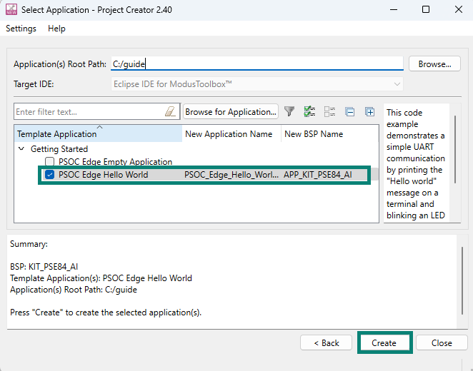
Select the application in the
Select Application window
and click
Create.
Figure 9.
New application creation
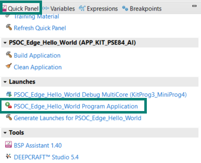
To build and program a PSOC™ Edge E84 MCU application in the Project Explorer, select
<App_Name> project
. In the
Quick Panel
, scroll to the
Launches
section and click the
<App_Name> Program Application
, as shown in the following figure.
Figure 10.
Programming in ModusToolbox™
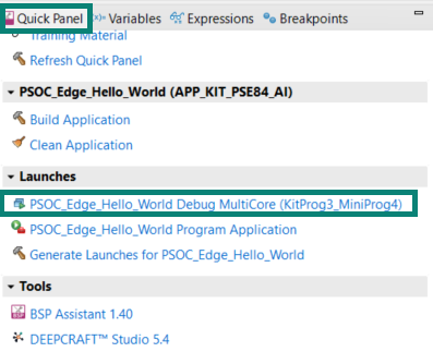
ModusToolbox™ has an integrated debugger. To debug a PSOC™ Edge E84 MCU application in the Project Explorer, select the
<App_Name>
project. In the
Quick Panel
, scroll to the
Launches
section and click the
<App_Name> Debug MultiCore(KitProg3_MiniProg4)
configuration as shown in the following figure. For a detailed explanation on how to debug using ModusToolbox™, refer
ModusToolbox™ user guide
.
Figure 11.
Debugging in ModusToolbox™
Hardware
Schematics
Hardware functional description
Power supply sub system
Power supply inputs
The power supply system on this board is versatile, allowing the board to be supplied from any of the following sources:
5 V input from on board KitProg3 Type-C USB connector ( J1 )
5 V input from the PSOC™ Edge E84 MCU Type-C USB connector ( J2 )
3 V - 5 V from the external/Battery power input connector ( J3 ) - by default this connector is not populated
The power supply system is designed to provide 1.8 V (core and I/O), and 3.3 V (I/O) operating voltages to the PSOC™ Edge E84 MCU and 5 V for the PSOC™ 5LP based KitProg3 operation. In addition, the voltages of 1.8 V, 3.3 V, and 5 V rails are also used for the operation of PSOC™ Edge E84 MCU, memory, and various sensors available on the kit.
Figure 12.
Block diagram of power architecture
Figure 13.
Schematic of power supply inputs of evaluation kit
The KitProg3 Type-C USB connector (
J1
) and PSOC™ Edge E84 device USB connector (
J2
) can only provide 5 V/3 A, as it is hard configured by pulling the CC1 and CC2 lines of
J1
connector to GND by the 5.1 KΩ pull-down resistor (
R3
, and
R4
) and for J2 the CC1 and CC2 lines are controlled by DRP controller (
U21
).
Figure 14.
Schematic of DRP controller
PSOC™ Edge E84 device USB connector can also be used as host interface (when DRP controller detects the devices connected to
J2
) with auto switching of power supply and maximum host current is limited to
500mA
.
The supply rails KP_VBUS (5 V from
J1
), PE84_VBUS (5 V from
J2
), and VBAT_IN from battery input connector (
J3
) are combined into VCC_IN through ideal diode ‘OR’ing circuits (
U23
,
U26
, and
U27
), as shown in the following figure.
Figure 15.
Schematic of power supply Or'ing
The VCC_IN supply rail serves as an input to the switching and linear voltage regulator to power the different peripherals on the board.
Voltage regulators
There are five voltage regulators present on the board:
5V Boost regulator ( U29 ): Powers the USB host interface of PSOC™ Edge E84 device and next stage of voltage regulators
3.3V Buck regulator ( U13 ): Powers the Wi-Fi & Bluetooth® module VBAT power supply, PSOC Edge E84 device IO's supply, Audio DAC ( U28 ) and MIPI DSI compatible displays
1.8 V Buck regulator ( U34 ): Powers the PSOC™ Edge E84 device core and IO's power supply
3.3 V LDO linear voltage regulator ( U35 ): Powers the onboard RADAR sensor
1.8 V LDO linear voltage regulator ( U33 ): Powers the Analog domain of PSOC™ Edge E84 MCU and onboard RADAR sensor
VCC_IN rail powers the 5V Boost regulator ( U29 ). The VDD_5V rail powers a 3.3V Buck regulator (
U13
), 1.8V Buck regulator (
U34
), 3.3 V LDO linear voltage regulator (
U35
). VDD_3V3 rail powers a 1.8 V LDO linear voltage regulator (
U33
).
Figure 16.
Schematic of 5V Boost power supply regulator (U29)
Figure 17.
Schematic of 3.3V Buck power supply regulator (U13)
Figure 18.
Schematic of 1.8V Buck power supply regulator (U34)
Figure 19.
Schematic of 3.3 V and 1.8 V LDO linear voltage regulators (U35, U33)
PSOC™ 5LP-based KitProg3 programmer and debugger
PSOC™ 5LP-based KitProg3
The onboard PSOC™ 5LP (CY8C5868LTI-LP039 -
U2
) device is used as the KitProg3 programmer/debugger to program and debug the PSOC™ Edge E84 MCU. PSOC™ 5LP device is connected to the USB port of a PC through a Type-C USB connector, and to the SWD and other communication interfaces of the PSOC™ Edge E84 MCU.
For more information, see the following:
PSOC™ 5LP webpage
- CY8C58LPxx family datasheet
Figure 20.
Schematic of PSOC™ 5LP based KitProg3
KitProg3 serial interface with PSOC™ Edge E84
In addition to being used as an onboard programmer/debugger using the SWD/JTAG interface, the PSOC™ 5LP device also functions as an interface for the USB-UART and USB-I2C bridges. The USB-Serial pins of the PSOC™ 5LP devices are hard-wired to the I2C/UART pins of the PSOC™ Edge E84 MCU. The I2C pins are also available on the expansion I/O header, and connected to all I2C interface-based sensors. Therefore, the PSOC™ 5LP device can be used to control a sensor with the I2C interface and PSOC™ Edge E84 MCU.
PSOC™ 5LP signal | PSOC™ Edge E84 I/O (signal) | Logic level |
|---|---|---|
PE84_SWCLK | P6[3] | 1.8 V |
PE84_SWDIO | P6[2] | 1.8 V |
PE84_RST_L | XRES | 1.8 V |
I2C_SDA_1V8 | P8[1] | 1.8 V |
I2C_SCL_1V8 | P8[0] | 1.8 V |
MCU_UART_RX_KP_TX | P6[5] | 1.8 V |
MCU_UART_TX_KP_RX | P6[7] | 1.8 V |
KitProg3 onboard target voltage measurement
PSOC™ 5LP of KitProg3 uses an ADC to measure the onboard target voltage. Before the ADC input, there is a voltage divider to bring the target voltage within the dynamic range.
Figure 21.
Schematic of KitProg3 onboard target voltage monitoring circuit
This feature allows you to measure the target MCU voltage through KitProg3 using PSOC™ or ModusToolbox™ programmer tools.
KitProg3 programming mode selection button and status LED
There is a mode selection button (SW3) connected to the P1[2] pin of the PSOC™ 5LP device for programming mode selection. This button can be used to switch between Bulk and HID modes (see the
KitProg3 user guide
for details). The button works in an active LOW configuration and is shorted to GND when pressed.
PSOC™ 5LP has a status LED (D12, Amber) connected to its P1[4] pin of the PSOC™ 5LP device, which indicates the programming status. See the following table for a summary of the LED status:
KitProg3 programming modes | Status LED (D2) |
|---|---|
CMSIS-DAP/Bulk mode (default) | ON |
CMSIS-DAP/HID mode | RAMPING at 1 Hz |
Note:
Switching between the programming modes can be done through the
Firmware-loader
tool. For details, see Section Mode Switching in the
KitProg3 user guide
.
Figure 22.
Schematic of KitProg3 mode selection button (SW3) and status LED (D12)
PSOC™ Edge E84 MCU features
PSOC™ Edge E84 MCU is a dual-CPU microcontroller with a neural net companion processor, DSP capability, high-performance memory expansion capability, low-power analog subsystem with high-performance analog-to-digital conversion and low-power comparators, IoT connectivity, communication channels, and programmable analog and digital blocks. It also has audio and graphics blocks.
PSOC™ Edge E84 MCU has the following features:
High-performance compute, DSP, and machine learning (ML) blocks
Low-power CPU block for security, control, and communication
Security up to Infineon Edge Protect Category 4 (EPC 4); supported by Trusted Firmware‑M (TF‑M), and mbedTLS crypto acceleration package
Lock-step secured enclave protected Root-of-Trust (RoT), secured boot, secured firmware updates
Low-power operation: multiple power modes; DC-DC buck converter; dynamic voltage and frequency management
Optimizable power: independent voltage domains; selectable SRAM retention
Communications and connectivity: USB, SD host, Serial Memory Interface (SMIF), Ethernet, CAN FD, I3C, I2 C, UART, SPI
Graphics and audio blocks
Always-on power domain: Autonomous Analog with ADC, DAC, opamps, comparators, Acoustic Activity Detection (AAD)
Programmable GPIO pins: drive modes, strengths, and slew rates; over-voltage tolerant (OVT) pins for I2C compliance. Some ports have a smart I/O programmable logic array
ModusToolbox™ development environment; installable SDKs and libraries; industry-standard Arm® tools; RTOS support
PSOC™ Edge E84 MCU offers several key features that enable it to run the machine learning algorithms efficiently. These include a dual CPU subsystem for parallel processing, a large memory capacity for storing and processing datasets, low-power operation for battery-powered applications, flexible clocking options for timing control, high-speed data access and communication, analog processing capabilities, and programmable GPIOs for hardware control. For more details, see the PSOC™ Edge E84 MCU datasheet.
In addition, Infineon's broad portfolio of hardware, software, and tool solutions, combined with DEEPCRAFT™'s expertise in developing robust machine learning solutions for edge devices, making it easier to leverage the advanced opportunities from AI/ML. DEEPCRAFT™ Studio, an end-to-end development platform, is planned for ML model creation, training, and deployment. This platform will enable you to bring AI into various embedded applications, enhancing functionalities, control, energy efficiency, and privacy. With DEEPCRAFT™ AI, you can benefit from a faster time to market, serving a wide range of applications for global customers.
PSOC™ Edge E84 MCU power
PSOC™ Edge E84 MCU is designed to operate at low power, making it suitable for battery-powered applications. The powering section of the board includes the core and I/O domain power connections, decoupling capacitors, and ferrite beads to isolate the digital and analog domains.
The core and I/O domain power connections are designed to provide a stable and efficient power supply to the PSOC™ Edge E84 MCU. The core power supply is connected to the VCC_1V8 rail, while the I/O power supply is connected to both the VCC_3V3 and VCC_1V8 power rails. These power rails are designed to provide the required voltage levels for the core and I/O operations.
PSOC™ Edge E84 MCU power rail | Supply voltage rail |
|---|---|
VBAT | VCC_3V3 (3.3 V) |
VDDA, VDDIO7, VDDIO8 | VCC_1V8 (1.8 V from Linear regulator) |
VDDUSB | VCC_3V3 (3.3 V) |
VDD_VBAT | VCC_1V8 (1.8 V) |
VDDQ | VCC_1V8 (1.8 V) |
VDDD | VCC_1V8 (1.8 V) |
VDDIO_SMIF0, VDDIO_SMIF1, VDDIO1, VDDIO2, VDDIO3, VDDIO4, VDDIO5 | VCC_1V8 (1.8 V) |
VDDIO6 | VCC_3V3 (3.3 V) |
VCCD | 0.7 V/0.8 V/0.9 V (internal Buck regulator) |
Figure 23.
Schematic for PSOC™ Edge E84 MCU power rail connections
Ferrite beads are used to isolate the digital and analog domains, preventing interference between these two domains. They are placed on the power lines connecting the digital and analog domains, ensuring that the power supply remains stable and free from interference.
Decoupling capacitors are placed close to the power pins of the MCU to filter out high-frequency noise and prevent it from affecting the operation of the MCU. These capacitors maintain a stable power supply and improve the system's performance.
PSOC™ Edge E84 MCU I/O signals
The PSOC™ Edge E84 MCU features a comprehensive set of I/O ports designed to facilitate easy interfacing with various sensors and peripherals. PSOC™ Edge E84 MCU has
22 I/O ports
, each of which can be configured with different functions based on the application requirements (refer to the datasheet for the list of alternate functions supported by the I/Os of each port). Each I/O port of the PSOC™ Edge E84 MCU is associated with a dedicated power supply, enabling users to configure different I/O ports at different logic levels.
PSOC™ Edge E84 MCU I/O ports | PSOC™ Edge E84 MCU power rail | Logic level |
|---|---|---|
P0, P4 | VDDIO_SMIF1 (VDD_1V8) | 1.8 V |
P1, P2, P3, P5 | VDDIO_SMIF0 (VDD_1V8) | 1.8 V |
P6, P7 | VDDIO0 (VDD_1V8) | 1.8 V |
P8 | VDDIO1 (VDD_1V8) | 1.8 V |
P9, P20 | VDDIO2 (VDD_1V8) | 1.8 V |
P10, P11 | VDDIO3 (VDD_1V8) | 1.8 V |
P12, P21 | VDDIO4 (VDD_1V8) | 1.8 V |
P13, P14 | VDDIO7 (VCC_1V8) | 1.8 V |
P15 | VDDIO8 (VCC_1V8) | 1.8 V |
P16, P17 | VDDIO6 (VDD_3V3) | 3.3/1.8 V |
P18, P19 | VDDIO5 (VDD_1V8) | 1.8 V |
Figure 24.
Schematic of PSOC™ Edge E84 MCU I/O signals
PSOC™ Edge E84 MCU clock sources
The PSOC™ Edge E84 AI kit is designed to support advanced applications with its hardware features. It includes a
24 MHz
external clock source from a crystal oscillator (
Y3
) connected to
P7[4]
as primary clock source. A
17.2032 MHz
clock source from a crystal (
Y1
) connected to
P19[0]
and
P19[1]
and a
32.768 KHz
clock source from crystal (
Y2
) is connected to
P18[0]
,
P18[1]
to enable the ECO (External Crystal Oscillator) and WCO (Watch Crystal Oscillator) modes of the PSOC™ Edge E84 MCU.
The external clock source and ECO mode is used for high-performance clock generation, which is crucial for applications that require fast processing speeds. The WCO mode, on the other hand, is used for low-power operation, allowing the device to run at reduced power consumption while still maintaining accurate timekeeping.
For USB functionality, it is recommended to use an external clock source for precise clock generation. This is because USB communication requires a stable and precise clock signal to ensure reliable data transfer. The external clock source can be connected to the PSOC™ Edge E84 MCU's USB clock input, providing the necessary clock signal for USB operation.
By utilizing these features, the PSOC™ Edge E84 AI kit provides high-performance clock generation, low-power operation, and reliable USB communication, making it suitable for advanced applications.
Figure 25. Schematic of clock sources for External clock source, ECO and WCO of PSOC™ Edge E84 MCU
PSOC™ Edge E84 MCU programming/debugging interface
In the PSOC™ Edge E84 AI Board, a default programming/debugging interface is through the on board KitProg3 programmer/debugger. In addition, you can use an external programmer like MiniProg4 to program/debug PSOC™ Edge E84 device through this 10-pin header (
J4
) which is not populated by default.
Figure 26.
PSOC™ Edge E84 MCU SWD/JTAG header interface schematic
The interface circuit
D4
provides ESD protection, and
C54
provides filtered reference voltage for external programmer to detect the target voltage of the PSOC™ Edge E84 device.
Note:
Do not feed power to the board through this header. The
J4.1
needs to be used only for taking the target voltage reference.
PSOC™ Edge E84 MCU external memory interface
PSOC™ Edge E84 AI Kit has Infineon's Quad SPI NOR flash memory
S25HS512TFABHI013
(
U4
) of 512 Mb and Octal PSRAM memory
S70KS1283GABHI020
(
U3
) of 128Mb. The NOR flash is connected to the Quad SPI interface and PSRAM memory is connected to Octal SPI interface (which also support hyper bus interface) of the PSOC™ Edge E84 MCU. The NOR flash device supports 4-bit (Quad I/O) serial commands. The NOR flash device can be used for both data and code memory with execute-in-place (XIP) support and encryption.
Signal name | PSOC™ Edge E84 I/O | Logic level |
|---|---|---|
SMIF0_DATA0 | P1[0] | 1.8 V |
SMIF0_DATA1 | P1[1] | 1.8 V |
SMIF0_DATA2 | P1[2] | 1.8 V |
SMIF0_DATA3 | P1[3] | 1.8 V |
SMIF0_CLKP | SMIF0_CLK_P | 1.8 V |
SMIF0_CS | P2[0] | 1.8 V |
Figure 27.
Schematic of QSPI flash memory interface
Signal name | PSOC™ Edge E84 I/O | Logic level |
|---|---|---|
SMIF1_DATA0 | P4[0] | 1.8 V |
SMIF1_DATA1 | P4[1] | 1.8 V |
SMIF1_DATA2 | P4[2] | 1.8 V |
SMIF1_DATA3 | P4[3] | 1.8 V |
SMIF1_DATA4 | P4[4] | 1.8 V |
SMIF1_DATA5 | P4[5] | 1.8 V |
SMIF1_DATA6 | P4[6] | 1.8 V |
SMIF1_DATA7 | P4[7] | 1.8 V |
SMIF1_RWDS | SMIF1_RWDS | 1.8V |
SMIF1_CLKP | SMIF1_CLK_P | 1.8 V |
SMIF1_CLKN | SMIF1_CLK_N | 1.8 V |
SMIF1_CS | P0[1] | 1.8 V |
MEMORY_RST | P0[0] | 1.8V |
Figure 28.
Schematic of PSRAM memory Octal/Hyper-bus interface
PSOC™ Edge E84 MCU USB interface
The PSOC™ Edge E84 AI Evaluation Kit consists of a Type-C USB connector (
J2
) for the PSOC™ Edge E84 MCU supporting both device and host mode, which can also be used as a power source for the board, as mentioned in section
Power inputs and over voltage protection
. The USB lines are connected to the PSOC™ Edge E84 MCU through an ESD protection (
U30
). A USB-C DRP controller is used to switch power paths to power up board when connected to a USB host and to feed the power when an USB device is connected to
J2
.
Note:
When USB device is connected to
J2
, the maximum load current that can be supported for the USB device is limited to
500mA
.
Signal name | PSOC™ Edge E84 MCU I/O | Description |
|---|---|---|
PE84_USB_DP | USBDP | USB Data signals |
PE84_USB_DM | USBDM | USB Data signals |
PE84_USB_ID | P7[1] | USB Host/Device identification |
PE84_USB_CF | P8[3] | Over current fault signal |
PE84_USB_DIR | P7[3] | identification signal for detection of USB-C plug orientation |
PE84_USB_OUT1, PE84_USB_OUT2 | P7[5], P7[6] | when MCU is configured in device, these signals are used to detect the USB-C DFP current mode |
Figure 29.
Schematic for PSOC™ Edge E84 USB host/device interface and power supply
Figure 30.
Schematic for USB-C DRP controller
There are 2 LED's (
D11
,
D14
) which indicate the status of the PSOC™ Edge E84 USB connected to a device or host. LED
D11
will be turned ON when this USB-C is configured as host (DFP mode),
D12
will be on when configured as device (UFP mode).
Figure 31.
Schematic for USB-C Host/Device status LED's
PSOC™ Edge E84 MCU MIPI DSI interface
The kit has an on board MIPI-DSI display interface that supports a two-lane protocol that can go up to 1.5 Gbps speed per data lane. There is a Raspberry pi display compatible connector supporting MIPI-DSI interface (
J10
). For few of the display a separate power, and touch controller interface is provided, in such cases connector
J10
can be used for the display driver interface and
J16
for the capacitive touch driver interface.
Note:
J16
is not populated by default, if using the display which needs external power and touch controller interface consider of populating
J16.
The MIPI-DSI Raspberry-Pi Interface (
J10
) supports a wide range of standard Raspberry-Pi displays. The
list of supported/recommended displays
is mentioned in
Table 11
.
Display Type | Display Name/MPN (MFR) | Supported Through |
|---|---|---|
Raspberry-Pi compatible display 1 | 2.8 inch MIPI-DSI 480×6400 Capacitive Touch Display (Waveshare) | J 10 |
4 inch MIPI-DSI 800×480 Capacitive Touch Display (Waveshare) | J 10 | |
4.3 inch MIPI-DSI 800×480 Capacitive Touch Display (Waveshare) | J 10 | |
5 inch MIPI-DSI 800×480 Capacitive Touch Display (Waveshare) | J 10 | |
7 inch MIPI-DSI 800×480 Capacitive Touch Display (Waveshare) | J 10 , J16 | |
7 inch MIPI-DSI 1024×600 IPS Capacitive Touch Display (Waveshare) | J 10 , J16 |
Figure 32.
Schematic of MIPI-DSI interface
Sensor sub system
XENSIV™ Sensor subsystem
XENSIV™ digital barometric pressure sensor
The PSOC™ Edge E84 AI Kit contains Infineon's digital barometric pressure sensor (
U6
)
DPS368XTSA1
. The sensor uses an I2C interface to communicate, along with an interrupt signal,
PSEN_INT
. The default I2C address is
0x77
. To change the address to
0x76
, populate
R84
.
Signal name | PSOC™ Edge E84 I/O | Logic level |
|---|---|---|
I2C_SDA_1V8 | P8[1] | 1.8 V |
I2C_SCL_1V8 | P8[0] | 1.8 V |
PSEN_INT | P11[3] | 1.8 V |
Figure 33.
Schematic of digital XENSIV™ barometric pressure sensor interface
XENSIV™ MEMS digital microphones
The PSOC™ Edge E84 AI Kit contains Infineon's two digital PDM MEMS microphones (
U7
,
U8
)
IM73D122V01XTMA1
which share the same PDM bus.
Each PDM microphone has a SELECT pin. If this pin is connected to GND, the PDM data is available on the falling edge of the PDM clock. If this pin is connected to VDD, the PDM data is available on the rising edge of the PDM clock.
The left PDM microphone (
U8
) data is available on the falling edge of the PDM_CLK, as the SELECT pin is tied to GND. The right PDM microphone (
U7
) data is available on the rising edge of the
PDM_CLK
, as the
SELECT
pin is tied to VDD_1V8. The microphones are placed ~27 mm apart and are supplied from a 1.8 V (VDD_1V8) rail.
Signal name | PSOC™ Edge E84 I/O | Logic level |
|---|---|---|
PDM_CLK | P8[5] | 1.8 V |
PDM_DATA | P8[6] | 1.8 V |
Figure 34.
Schematic of digital microphones interface
XENSIV™ MEMS analog microphones
The PSOC™ Edge E84 AI kit contains two analog XENSIV™ MEMS microphones (
U9
,
U10
) IM73A135V01XTSA1 from Infineon Technologies which are designed for high SNR (low self-noise) and low distortion (high AOP) applications.
U10
is the left channel microphone and
U9
being the right channel, placed ~32 mm apart from each other. Both microphones are supplied from 1.8 V (VCC_1V8) rail.
Signal name | PSOC™ Edge E84 I/O |
|---|---|
AMIC1_CTB_INP | P14[0] |
AMIC1_CTB_INN | P14[1] |
AMIC1_CTB_OUT | P14[2] |
AMIC1_CTB_REF | P14[6] |
AMIC2_CTB_INP | P14[4] |
AMIC2_CTB_INN | P14[5] |
AMIC2_CTB_OUT | P14[3] |
AMIC2_CTB_REF | P14[7] |
Figure 35.
Schematic of analog microphones
XENSIV™ 60 GHz RADAR sensor
The PSOC™ Edge E84 AI Kit contains Infineon's XENSIV™ 60 GHz RADAR sensor (
U5
) BGT60TR13CE6327XUMA1. The BGT60TR13C MMIC is a 60 GHz radar sensor with integrated antennas; one transmitting and three receiving antennas. The sensor incorporates an L-shaped antenna array, ensuring both horizontal and vertical angular measurements. This sensor comes with an Antennas in Package (AIP) concept, which eliminates the antenna design complexity at the user end, and the PCB can be designed with standard FR4 materials. For more details, see the
RADAR sensor webpage
. The RADAR sensor uses an SPI interface to communicate, along with an interrupt signal (
RSPI_IRQ
) and reset signal (
RXRES_L
).
Signal name | PSOC™ Edge E84 IO | Logic level |
|---|---|---|
RSPI_CS | P21[7] | 1.8 V |
RSPI_CLK | P21[6] | 1.8 V |
RSPI_MOSI | P21[5] | 1.8 V |
RSPI_MISO | P21[4] | 1.8 V |
RSPI_IRQ | P20[3] | 1.8 V |
RXRES_L | P20[7] | 1.8 V |
Figure 36.
Schematic of RADAR sensor interface
The RADAR sensor uses power supply filters, including ferrite beads and various capacitors, as shown in the following figure.
Figure 37.
Schematic RADAR sensor power supply filtering
The following figure shows how an onboard crystal oscillator (
U24
) feeds 80 MHz clock input to the RADAR sensor.
Figure 38.
Schematic of crystal oscillator for RADAR sensor clock input
6-axis IMU
6-axis IMU (accelerometer + gyroscope) for acceleration and gyroscopic angular rate sensing in each spatial direction.
This kit contains a 6-axis motion sensor (
U18
), also known as the inertial measurement unit (
IMU
), which provides precise 3-axis acceleration and 3-axis gyroscopic angular rate data in each spatial direction. The sensor uses an I2C interface to communicate, along with two interrupt signals, which are connected to the
IMU_
INT1
and
IMU_
INT2
pins of the sensor to the PSOC™ Edge E84 MCU by default. The default I2C secondary address is
0x68
(also configurable to
0x69
by removing
R86
and populating
R85
).
Signal name | PSOC™ Edge E84 I/O | Logic level |
|---|---|---|
I2C_SDA_1V8 | P8[1] | 1.8 V |
I2C_SCL_1V8 | P8[0] | 1.8 V |
IMU_INT1 | P7[7] | 1.8 V |
IMU_INT2 | P6[6] | 1.8 V |
Figure 39.
Schematic of 6-axis IMU (accelerometer + gyroscope)
3-axis Geo-magnetic sensor
This kit contains a 3-axis magnetometer sensor (
U20
), which is for sensing the direction and strength of the geomagnetic field. The sensor uses an I3C interface to communicate with PSOC™ Edge E84 device, along with an interrupt signal
MAG_INT
by default. The I3C address is configured to
0x15
. This sensor interface can be configured to I2C by rework of resistor
R220
and
R223
.
Signal name | PSOC™ Edge E84 I/O | Logic level |
|---|---|---|
I3C_SDA | P3[1] | 1.8 V |
I3C_SCL | P3[0] | 1.8 V |
MAG_INT | P6[4] | 1.8 V |
Figure 40.
Schematic of a 3-axis magnetometer
Digital Humidity sensor
This kit features a digital humidity sensor SHT40 (
U22
), which comes equipped with a built-in temperature sensor. This sensor communicates with the PSOC™ Edge E84 MCU via the I
2
C interface. The default I2C address for this sensor is
0x44
. This sensor is powered with 1.8 V supply from the rail
VDD_1V8
.
Signal name | PSOC™ Edge E84 I/O | Logic level |
|---|---|---|
I2C_SDA_1V8 | P8[1] | 1.8 V |
I2C_SCL_1V8 | P8[0] | 1.8 V |
Figure 41.
Schematic of the digital humidity sensor interface
Reset and user buttons
This Kit contains one reset button (
SW2
) for resetting the PSOC™ Edge E84 MCU. When this
SW2
button is pressed, the
PE84_RST_L
line of the PSOC™ Edge E84 MCU is pulled to the ground, which in turn resets the target device. The
4.7K
pull-up resistor on the
PE84_RST_L
is populated on the kit.
Figure 42.
Schematic for Reset button interface
The board features a user button
SW1
, which serves as a general user input or for controlling different application states. The PSOC™ Edge E84 MCU pin
P7[0]
connected to user button
SW1
is pulled to the ground through a
1K
resistor when this button is pressed.
Figure 43.
Schematic for User button interface
User LED's and Power LED's
The kit contains two discrete user LEDs:
LED1
(GREEN),
LED2
(BLUE), one user RGB LED (
LED3
)
and a power LED
LED5
(AMBER) for indication.
The power LED (
LED5
) indicates that the board is powered from either the on board KitProg3 Type-C USB connector (
J1
), PSOC™ Edge E84 Type-C USB connector (
J2
), or external power/battery input connector (
J3
).
Figure 44.
Schematic for power LED
The user LED’s (
LED1
and
LED2
) and user RGB LED (
LED3
) are connected to I/O's of the PSOC™ Edge E84 MCU, respectively. The user LED’s are active HIGH, so the pins must be driven HIGH to turn ON the LED’s.
Signal name | PSOC™ Edge E84 I/O | Logic level |
|---|---|---|
USER_LED1 | P10[7] | 1.8 V |
USER_LED2 | P10[5] | 1.8 V |
USER_LED_RGB_R | P20[6] | 1.8 V |
USER_LED_RGB_G | P20[4] | 1.8 V |
USER_LED_RGB_B | P20[5] | 1.8 V |
Figure 45.
Schematic of user LED’s
Wi-Fi® 6 & Bluetooth® LE 5.4 Dual-Radio module interface
The LBEE5HY2FY SiP (system-in-package) module (2FY module), powered by the Infineon CYW55513 chipset, is a dual-mode wireless solution that offers Wi-Fi® 802.11a/b/g/n/ac/ax + Bluetooth® 5.4 BR/EDR/LE up to 143Mbps PHY data rate on Wi-Fi, 3Mbps PHY data rate on Bluetooth and 2Mbps PHY data rate on Bluetooth® LE. The WLAN section supports SDIO 3.0 interface and the Bluetooth® section supports high-speed 4-wire UART interface. This module is designed for easy integration into various applications, providing reliable and high-speed wireless connectivity.
The 2FY module is powered with an external VBAT supply voltage of 3.3 V and an I/O's supply voltage of 1.8 V for interface IOs.
Figure 46.
2FY module power supply schematic
PSOC™ Edge E84 device communicates to 2FY module using a standard SDIO interface for WLAN and UART interface for Bluetooth® operation. PSOC™ Edge E84 device interface with 2FY module supports the following features.
2FY module signal | PSOC™ Edge E84 MCU I/O | Description |
|---|---|---|
BT_REG_ON | P11[0] | BT_REG_ON signal controlled by PSOC™ Edge E84 device I/O used to power up or power down the internal regulators used by the Bluetooth® section. Also, when deasserted, this pin holds the Bluetooth® section in reset. |
WL_REG_ON | P11[4] | WL_REG_ON signal controlled by PSOC™ Edge E84 device I/O used to power up or power down the internal regulators used by the WLAN section. Also, when deasserted, this pin holds the WLAN section in reset. |
WL_HOST_WAKE | P11[6] | Wi-Fi HOST_WAKE or general-purpose I/O signal |
BT_HOST_WAKE | P10[4] | Bluetooth® HOST_WAKE or general-purpose I/O signal |
BT_DEV_WAKE | P10[6] | DEV_WAKE or general-purpose I/O signal |
SDIO_CLK | P12[0] | SDIO clock input |
SDIO_CMD | P21[0] | SDIO command line |
SDIO_DATA[0] | P12[1] | SDIO Data lines |
SDIO_DATA[1] | P12[2] | SDIO Data lines |
SDIO_DATA[2] | P12[4] | SDIO Data lines |
SDIO_DATA[3] | P12[5] | SDIO Data lines |
BT_UART_TXD | P10[0] | UART serial output. Serial data output for the HCI UART interface. |
BT_UART_RXD | P10[1] | UART serial input. Serial data input for the HCI UART interface. |
BT_UART_CTS | P10[3] | UART clear-to-send. Active-low clear-to-send signal for the HCI UART interface. |
BT_UART_RTS | P10[2] | UART request-to-send. Active-low request to send signal for the HCI UART interface. |
Figure 47.
2FY module interface schematic
An on board oscillator (
Y4
) of 32.768 KHz is used to provide external clock input (
LPO_OUT_2FY
) to the 2FY module.
Figure 48.
External LPO schematic
2FY module antenna output is connected to an on board chip antenna with a matching circuit, as shown in the following figure.
Figure 49.
2FY module RF front-end schematic
I/O expansion header
Digital I/O interface header
There is a 100 mil pitch expansion headers (
J14
) which provide connectivity to a few of the PSOC™ Edge E84 MCU GPIOs compatible with 3.3 V I/O logic level.
Figure 50.
Schematic of the expansion header
Note:
This digital I/O interface header has signal
P11_1_IN_3V3
which supports only input functionality.
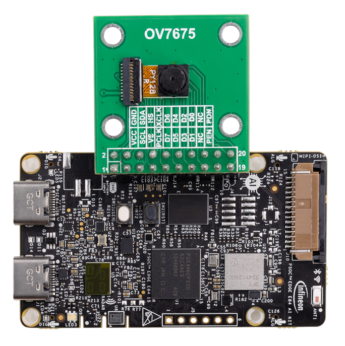
This header (
J14
) can be used to interface the OV7675 DVP camera module which is provided as part of the kit. A level translator circuit is used to convert the 3.3 V I/O logic level signal coming from the header (
J14
) pin number
13
connected to MCU I/O pin
P11[1]
to support the PCLK function of DVP camera module interface.
Figure 51.
Schematic of the level translator
Figure 52.
Connecting the DVP camera module to PSOC™ Edge E84 AI board
Analog I/O interface header
There is a 0.4mm pitch connector (
J17
) which provide connectivity to a few I/O's supporting analog functionality of the PSOC™ Edge E84 MCU GPIOs compatible with 1.8 V I/O logic level. By default this connector (
J17
) is not populated.
Figure 53.
Schematic of the expansion header
Boot Options and Alternate serial interface header
There is a 1-bit boot configuration resistor provision (
R187
and
R188
) that sets the boot location for the PSOC™ Edge E84 MCU. The resistor provision output is connected to the
P17[6]
pin of the PSOC™ Edge E84, whose state is read by the MCU, and based on that, the boot location is set. See
Table 21
for the boot source options. By default, the resistor position is set to provide logic 1 (ON - R188 is populated).
Resistor Populated | Boot location |
|---|---|
R187 Populated - logic level at P17[6] is 0 (OFF) | Internal RRAM |
R188 Populated - logic level at P17[6] is 1 (ON, Default) | External FLASH (On board QSPI flash memory) |
Figure 54.
Schematic of boot configuration resistor provision
There is an 100mil pitch single row header (
J5
) which is used as GPIO interface by default. This header can also be used as alternate serial interface to program PSOC Edge E84 MCU by configuring the resistor provisions as show in the figure
Figure 55.
Schematic of Alternate serial interface configuration resistor provision
Figure 56.
Schematic of Alternate serial interface header
I2C interface connector
The PSOC™ Edge E84 AI kit comes with a 4-pin connector (
J7
) designed to extend the I2C interface from the PSOC™ Edge E84 MCU. The extension capability is specifically for adding I2C-based add-on boards.
This interface connector is compatible with QWIIC connection system boards, a product of SparkFun. By using the 4-pin connector, you can attach the QWIIC boards to the PSOC™ Edge E84 MCU. This expands the functionality of the PSOC™ Edge E84 MCU, as it allows it to connect and interact with multiple system boards that support the QWIIC system.
Note:
By default this header is not populated, to enable this interface
J7
connector has to populated.
Figure 57.
Schematic of I2C interface connector
Pin details | PSOC™ Edge E84 I/O | Logic level |
|---|---|---|
J7.3 | P17[1] (I2C_SDA_3V3) | 3.3 V |
J7.4 | P17[0] (I2C_SCL_3V3) | 3.3 V |
Audio Class-D amplifier
The kit contains an audio amplifier (
U28
), which is a low-power, highly integrated, high-performance stereo audio DAC with 24-bit stereo playback and digital audio processing blocks which supports of 8KHz to 192KHz sampling rates. It contains a Class-D BTL mono speaker driver and a Class A/B stereo headphone driver. The amplifier is connected to a 2pin connector (
J8
) which can drive upto 2.5 W mono speaker.
Additionally, there is a pair of test points (
TP24
,
TP25
) for analog input L/R channels which can be used as input for analog audio signal. The amplifier is interfaced with PSOC™ Edge E84 MCU on the EVK via an I2S interface for audio data communication and an I2C interface which provides control and full access on the registers and the state machines. The amplifier’s DVDD, IOVDD domains are supplied from 1.8 V (VDD_1V8); AVDD, HPVDD domains are supplied from 3.3 V (VDD_3V3) and SPKVDD domain from 5 V (VDD_5V). The I2C device slave address is
0x18
.
Signal name | PSOC™ Edge E84 I/O | Logic level |
|---|---|---|
I2S_TX_MCK (I2S MCLK) | P21[3] | 1.8 V |
I2S_TX_SCK (I2S Clock) | P21[2] | 1.8 V |
I2S_TX_SD (I2S data input) | P21[1] | 1.8 V |
I2S_TX_FSYNC (I2S word select) | P12[3] | 1.8 V |
Figure 58.
Schematic of audio class-D amplifier
KIT_PSE84_AI kit rework for evaluating additional features
Enabling the external programming/debugging interface
The default programming/debugging interface for the
PSOC™
Edge E84 device is the on board KitProg3. A 10-pin header (
J4
) is provided on the kit to interface with an external programmer, such as MiniProg4. By populating the
J4
header, MiniProg4 can be directly connected to the PSOC™ Edge E84 device.
Reference | Description | Manufacturer | Manufacturer part number |
|---|---|---|---|
J4 | CONN, HDR, MALE, DUAL, 10POS, 1.27 mm, GOLD, STR, SMD | Samtec | FTSH-105-01-L-DV-K-P-TR |
shows the reworked schematic sections.
Figure 59.
Schematic of rework regions to enable the external programming interface
Pin details | Kit function | MiniProg4 interface function |
|---|---|---|
J4.1 | VTAR_REF, PSOC™ Edge E84 device voltage reference | VTARG, to sense the target MCU voltage |
J4.2 | P6[2], Port 6 Pin 2, is a GPIO of the PSOC™ Edge E84 device that supports the SWD interface and is connected to the target MCU via the SWDIO signal. | SWDIO, SWD data in/out interface with the target MCU |
J4.3 | GND, ground reference of prototyping board | GND, ground reference of MiniProg4 |
J4.4 | P6[3], Port 6 Pin 3, is a GPIO of the PSOC™ Edge E84 device that supports the SWD interface and is connected to the target MCU via the SWDCLK signal. | SWDCLK, SWD clock interface with the target MCU |
J4.5 | GND, ground reference of the prototyping board | GND, ground reference of MiniProg4 |
J4.6 | P6[0], Port 6 Pin 0, is a GPIO of the PSOC™ Edge E84 device that supports the SWD interface and is connected to the target MCU via the SWO signal. Also support TDO signal of JTAG interface. | SWO, serial wire output signal of SWD interface and TDO signal of JTAG interface with the target MCU |
J4.7 | GND, ground reference of the prototyping board | GND, ground reference of MiniProg4 |
J4.8 | P6[1], Port 6 Pin 1, is a GPIO of the PSOC™ Edge E84 device that supports the JTAG interface and is connected to the target MCU via the TDI signal. | TDI signal of JTAG interface with the target MCU |
J4.9 | GND, ground reference of the prototyping board | GND, ground reference of MiniProg4 |
J4.10 | XRES_L, reset signal for the PSOC™ Edge E84 device | XRES, reset signal for the target MCU |
Enabling addition Boot configurations
There is a 1-bit boot configuration resistor provision (
R187
and
R188
) that sets the boot location for the PSOC™ Edge E84 MCU. The resistor provision output is connected to the
P17[6]
pin of the PSOC™ Edge E84, whose state is read by the MCU, and based on that, the boot location is set. By default, the resistor position is set to provide logic 1 (ON - R188 is populated).
Resistor Populated | Boot location |
|---|---|
R187 Populated - logic level at P17[6] is 0 (OFF) | Internal RRAM |
R188 Populated - logic level at P17[6] is 1 (ON, Default) | External FLASH (On board QSPI flash memory) |
Figure 60.
Schematic of boot configuration resistor provision
Enabling the alternate serial interface
There is an 100mil pitch single row header (
J5
) which is used as GPIO interface by default. This header can also be used as alternate serial interface to program PSOC Edge E84 MCU by configuring the resistor provisions as show in the figure
Figure 61
will enable the alternate serial interface with UART, SPI, I2C and USB.
Reference | Description | Manufacturer | Manufacturer part number |
|---|---|---|---|
R76, R77, R79, R80 | RES, Fixed, 4.7K, 5%, 1/10W, 0603 | Wurth | 560112116045 |
J5 | CONN, HEADER, VERT, 6POS, 2.54MM, TH | Sullins | PRPC006SFAN-RC |
Figure 61.
Schematic of Alternate serial interface configuration resistor provision
Figure 62.
Schematic of Alternate serial interface header
Enabling external powering option
A external/Battery power input connector (
J3
) provide on board to power the board from external power source of voltage ranging from 3V to 5V.
J3
connector is also can be used to connect an external lithium ion battery. By default
J3
connector is not populated and to use this feature, need to populate the
J3
connector and populate
D15
TVS diode.
Reference | Description | Manufacturer | Manufacturer part number |
|---|---|---|---|
J3 | CONN, HDR, 1x2POS, SHROUNDED, R/A, 2MM PITCH, SMT | Wurth | 620102131822 |
D15 | DIODE, TVS, 17.3V, 15A, SOD-523 | Diodes Incorporated | T5V0S5A-7 |
shows the reworked schematic sections.
Figure 63. Schematic of rework regions to enable the external power input for the PSOC™ Edge E84 device
Enabling external I2C device interface
The PSOC™ Edge E84 AI kit features a 4-pin connector (
J7
) that extends the I2C interface of the PSOC™ Edge E84 MCU, enabling the addition of external I2C-based add-on boards. This connector is compatible with the QWIIC connection system by SparkFun, offering a plug-and-play method to connect QWIIC interface compatible boards without the need for soldering or complex wiring.
Reference | Description | Manufacturer | Manufacturer part number |
|---|---|---|---|
J7 | CONN, HEADER, R/A, 4POS, 1MM, SMD | Wurth | 620102131822 |
shows the reworked schematic sections.
Figure 64.
Schematic of rework regions to enable the external I2C device interface
Pin details | Kit function |
|---|---|
J7.1 | connected to ground rail |
J7.2 | connected to 3.3 V power rail |
J7.3 | P17[1], Port 17 Pin 1, is a GPIO of the PSOC™ Edge E84 device that supports I2C interface and is connected to I2C SDA signal of MCU |
J7.4 | P17[0], Port 17 Pin 0, is a GPIO of the PSOC™ Edge E84 device that supports I2C interface and is connected to I2C CLK signal of MCU |
Enabling Analog I/O interface
There is a 0.4mm pitch connector (
J17
) which provide connectivity to a few I/O's supporting analog functionality of the PSOC™ Edge E84 MCU GPIOs compatible with 1.8 V I/O logic level. By default this connector (
J17
) is not populated. To enable this analog I/O interface the following connector (
J17
) has to be populated.
Reference | Description | Manufacturer | Manufacturer part number |
|---|---|---|---|
J17 | CONN, PLUG, DUAL, 20POS, 0.4mm, SMD, GOLD | Hirose Electric Co Ltd | DF40C-20DP-0.4V(51) |
Figure 65.
Schematic of the expansion header
Enabling the Speaker interface
To enable the speaker interface, ensure the
J8 connector
is populated to connect a mono speaker (up to 2.5 W). The Class-D BTL mono speaker driver is powered by the
SPKVDD domain
, which is already supplied with
5 V (VDD_5V)
on the board. The amplifier communicates with the MCU via the
I2S interface
for audio data and the
I2C interface
(slave address 0x18) for control and configuration. Proper initialization through the I2C interface is necessary to activate the Class-D driver and enable the speaker output.
Details about the
J8 connector
can be found in the rework section below.
Reference | Description | Manufacturer | Manufacturer part number |
|---|---|---|---|
J8 | CONN, HDR, MALE, R/A, 2POS, 1.25MM, SMD | Molex | 532610271 |
Figure 66.
Schematic of audio class-D amplifier with speaker interface connector
Enabling the external power and I2C interface for MIPI DSI displays
To enable the external power and I2C interface for
MIPI DSI displays
, ensure the
J16 connector
(
TSM-102-01-L-DH-A-P-TR
) is populated. This connector provides a
5 V supply
and an
I2C interface
necessary for enabling compatibility with select MIPI DSI Raspberry Pi interface displays that require external power and I2C for touch functionality. The 5 V power is supplied directly through the board, while the I2C interface allows communication for touch-related operations. Proper initialization of the I2C interface is required to ensure seamless functionality with the connected display.
Details about the
J16 connector
can be found in the rework section below.
Reference | Description | Manufacturer | Manufacturer part number |
|---|---|---|---|
J16 | CONN, HDR, MALE, 4 POS, 2.54 MM, GOLD, RA, SMD | Samtec | TSM-102-01-L-DH-A-P-TR |
Figure 67.
Schematic of MIPI-DSI interface with external power and I2C interface header
Bill of materials
Glossary
ADC
Analog-to-Digital Converter
BOM
Bill of Materials
CTS
Clear To Send
DAC
Digital to Analog Conversion
DC
Direct Current
DSI
Display Serial Interface
ECO
External Crystal Oscillator
ESD
Electrostatic Discharge
GPIO
General-Purpose Input/Output
IC
Integrated Circuit
IDE
Integrated Development Environment
IMU
Inertial Measurement Unit
I/O
Input/Output
IoT
Internet of Things
I2C
Inter-integrated Circuit
I2S
Inter-IC Sound
I3C
Improved Inter-Integrated Circuit
JTAG
Joint Test Action Group
LED
Light-emitting Diode
LPO
Low Power Oscillator
MCU
Microcontroller Unit
MEMS
Micro Electro Mechanical systems
MIPI
Mobile Industry Processor Interface
OSPI
Octal Serial Peripheral Interface
OVP
Overvoltage Protection
PC
Personal Computer
PD
Power Delivery
PDL
Peripheral Driver Library
PDM
Pulse Density Modulation
PSOC™
Programmable System-on-Chip
PMU
Power Management Unit
QSPI
Quad Serial Peripheral Interface
RAM
Random Access Memory
RC
Resistor Capacitor
RTS
Ready To Send
RX
Receiver
SCL
Serial Clock
SD
SD card
SDA
Serial Data
SDIO
Secure Digital Input Output
SDK
Software Development Kit
SMIF
Serial Memory Interface
SPI
Serial Peripheral Interface
SWCLK
Serial Wire Clock
SWD
Serial Wire Debug
SWDIO
Serial Wire Debug Input Output
SWO
Serial Wire Out
SRAM
Static Random-Access Memory
TX
Transmitter
UART
Universal Asynchronous Receiver Transmitter
USB
Universal Serial Bus
WCO
Watch Crystal Oscillator
WLAN
Wireless LAN
R-Pi
Raspberry Pi
XRES
External Reset
Revision history
Document version | Date of release | Description of changes |
|---|---|---|
** | 2025-08-12 | Initial release |
*A | 2025-09-25 | Updated links in the document |
Trademarks
PSOC™, formerly known as PSoC™, is a trademark of Infineon Technologies. Any references to PSoC™ in this document or others shall be deemed to refer to PSOC™.
1
May support any other R-Pi-compatible display that complies with the standard 15-pin R-Pi pin out.