Datasheet
LITIX™ Basic+
Product images
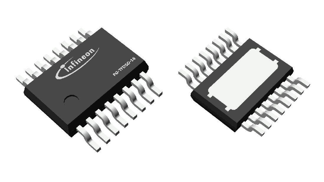
Images [Cover-Images]


Features
- Three-channel device with integrated and protected output stages (current sinks), optimized to drive LEDs
- High output current up to 150 mA per channel
- Possibility to offload power consumption via low cost external resistors to allow maximum current driving capability (Power Shift)
- Output current control via enable pin
- Fault management supports both 1-fail-all-OFF and 1-fail-all-ON
- Analog output current control input to adjust the output current
- Open load (OL), short to battery (SC) and thermal shutdown protections
- Intelligent fault management: up to 10 devices can share a common error network with only one external resistor
- Thermal derating function via external NTC resistor
Potential applications
- Cost effective "stop"/"tail" function with shared and separated LEDs per function
- Automotive light functions like turn indicators, position, fog, stop/tail, DRL and side markers
- Animated light functions like sequential indicator and "welcome/goodbye" functions
- Interior lighting functions like ambient lighting, illumination and dash board lighting
- LED indicators for industrial applications and instrumentation
Product validation
Product validation according to AEC-Q100, Grade 1.
Qualified for automotive applications.
Description
The TLD2372-3ET is a three channel low-side driver IC with integrated and protected output stages. It is designed to control LEDs with a current up to 150 mA as linear current sink (LCS). The Power Shift feature allows the device to reach maximum current driving capability by offloading power consumption to external low cost components. The diagnostic features and thermal derating via external NTC resistor provide a reliable solution for high current applications. The configurable fault management allows up to 10 and more devices to share the same error network and to be combined in applications with other LITIX™ LED drivers, such as other LITIX™ Basic+ products and LITIX™ TLD7002-16ES.
| Product type | Package | Marking |
|---|---|---|
| TLD2372-3ET | TFDSO-16 | 237 |
Product description
| Parameter | Symbol | Values |
|---|---|---|
| Operating voltage | VS(func) | 5.5 V - 18 V |
| Extended operating voltage | VS(ext) | 4.5 V - 36 V |
| Maximum load current | ISENSE(max) | 150 mA |
| Output current accuracy | VSENSE(reg) | ±4% with VSENSE = 400 mV |
| Current consumption in sleep mode | IVS(sleep, max) | 3 μA |
| Maximum current consumption during fault | IVS(fault, ERRN) | 850 μA |
| Maximum dropout voltage | VDR,CS(max) | 0.6 V |
Block diagram
Pin configuration
Pin assignment
Pin definitions and functions
| Pin | Symbol | Function |
|---|---|---|
| 16 | VS |
Power supply voltage Battery supply input |
| 4 | GND |
Ground Ground potential. Connect externally close to the chip |
| 1 | EN/DEN |
Output enable and diagnosis control input Connect to VS via a resistor divider to enable all outputs control and diagnosis capability |
| 2 | D |
Disable/delay error input Connect to a capacitor, leave open or connect to GND depending on the required diagnostic management |
| 3 | IREF |
Current reference generation Connect to an external accurate low power resistor to generate a current reference |
| 9 | ERRN/DEN |
ERROR flag I/O and diagnosis control input Open drain, active low. Connect to VS via pull-up resistor for ERROR flag capability only otherwise connect to VS via a resistor divider to enable diagnosis capability |
| 6 | SENSE1 |
Sense input 1 Connect to low ohmic accurate sense resistor |
| 7 | SENSE2 |
Sense input 2 Connect to low ohmic accurate sense resistor |
| 8 | SENSE3 |
Sense input 3 Connect to low ohmic accurate sense resistor |
| 14 | OUT1 |
Channel 1, output pin Open drain linear current sink. Connect to the target load |
| 15 | PS1 |
Power shift 1 Connect to external power resistor |
| 12 | OUT2 |
Channel 2, output pin Open drain linear current sink. Connect to the target load |
| 13 | PS2 |
Power shift 2 Connect to external power resistor |
| 10 | OUT3 |
Channel 3, output pin Open drain linear current sink. Connect to the target load |
| 11 | PS3 |
Power shift 3 Connect to external power resistor |
| 5 | ACC/PWMI |
Analog current control and PWMI input pin Connect to external low power resistor or apply a desired reference voltage to adjust the output current. Connect to external NTC to apply thermal derating. It is possible also to connect to an external open drain PWM controller |
| Exposed pad | EP |
Exposed pad Used only for thermal dissipation purpose. Connect externally to GND close to the chip |
General product characteristics
Absolute maximum ratings
| Parameter | Symbol | Values | Unit | Note or condition | P-Number | ||
|---|---|---|---|---|---|---|---|
| Min. | Typ. | Max. | |||||
Voltages |
|||||||
Supply voltage | VS | -0.3 | – | 40 | V | – | PRQ-32 |
EN/DEN voltage | VEN/DEN | -0.3 | – | 40 | V | – | PRQ-55 |
Output voltages | VOUTx | -0.3 | – | 40 | V | – | PRQ-58 |
Power shift voltages | VPSx | -0.3 | – | 40 | V | – | PRQ-60 |
Sense voltage | VSENSEx | -0.3 | – | 0.9 | V | – | PRQ-62 |
ERRN/DEN voltage | VERRN/DEN | -0.3 | – | 40 | V | – | PRQ-61 |
D voltage | VD | -0.3 | – | 5.5 | V | – | PRQ-175 |
ACC/PWMI voltage | VACC/PWMI | -0.3 | – | 5.5 | V | – | PRQ-64 |
IREF voltage | VIREF | -0.3 | – | 5.5 | V | – | PRQ-176 |
Temperatures |
|||||||
Junction temperature | TJ_ABS | -40 | – | 150 | °C | – | PRQ-39 |
Storage temperature | TSTG | -55 | – | 150 | – | – | PRQ-40 |
ESD robustness |
|||||||
ESD robustness all pins (HBM) | VESD(HBM) | -2 | – | 2 | kV | ESD robustness, Human Body Model “HBM” according to AEC Q100-002 | PRQ-53 |
ESD robustness all pins (CDM) | VESD(CDM) | -500 | – | 500 | V | ESD robustness, Charged Device Model “CDM” according to AEC Q100-011 Rev.D | PRQ-41 |
ESD robustness corner pins (CDM) | VESD(CDM) CR | -750 | – | 750 | V | ESD robustness, Charged Device Model “CDM” according to AEC Q100-011 Rev.D | PRQ-54 |
Stresses above the ones listed here may cause permanent damage to the device. Exposure to absolute maximum rating conditions for extended periods of time may affect device reliability.
Integrated protection functions are designed to prevent IC destruction under fault conditions described in the data sheet. Fault conditions are considered as outside the normal operating range. Protection functions are not designed for continuous repetitive operation.
Functional range
| Parameter | Symbol | Values | Unit | Note or condition | P-Number | ||
|---|---|---|---|---|---|---|---|
| Min. | Typ. | Max. | |||||
Voltages |
|||||||
Supply voltage for operating range | VS(func) | 5.5 | – | 18 | V | – | PRQ-33 |
Extended supply voltage for operating range | VS(ext) | 4.5 | – | 36 | V | – | PRQ-71 |
Currents |
|||||||
Channel output current | ISENSEx(func) | 5 | – | 150 | mA | – | PRQ-223 |
Power dissipation |
|||||||
Max. static and dynamic power dissipation | Pmax | – | – | 1.5 | W | TA = 85°C and RthJA = 40 K/W | PRQ-178 |
Temperatures |
|||||||
Junction temperature | TJ(func) | -40 | – | 150 | °C | – | PRQ-72 |
Within the functional or operating range, the IC operates as described in the circuit description. Within the Extended Operation range, parameters deviations are possible. The electrical characteristics are specified within the conditions given in the electrical characteristics table.
Thermal resistance
This thermal data was generated in accordance with JEDEC JESD51 standards. For more information, go to www.jedec.org
| Parameter | Symbol | Values | Unit | Note or condition | P-Number | ||
|---|---|---|---|---|---|---|---|
| Min. | Typ. | Max. | |||||
Junction to top | ΨJTOP | – | 7 | – | K/W | PRQ-262 | |
Junction to case | RthJC |
– | 6 |
– | K/W | PRQ-263 | |
Junction to ambient 1s0p board | RthJA1 | – | 61 | – | K/W | TA = 85°C | PRQ-264 |
Junction to ambient 2s2p board | RthJA2 | – | 40 | – | K/W | TA = 85°C | PRQ-265 |
Internal supply
This chapter describes the internal supply, its main parameters and functionality.
Description
As soon as the voltage applied at the supply pin VS is above VSUV(th) and the voltage applied at the EN/DEN pin is above VEN(th), the device is ready to deliver output current from the output stage after the power on reset time tPOR. When the supply voltage VS is below the threshold VSUV(th), the internal Power-ON-Reset (POR) function holds the device in reset state.
The power on reset time tPOR has to be taken into account under relevant application conditions, i.e. with PWM control from VS.
If the voltage applied at the EN/DEN pin is below VEN(th) for more than tSLEEP the device enters sleep mode. In this state all internal functions are switched off and the current consumption is reduced to IVS(sleep).
Electrical characteristics
| Parameter | Symbol | Values | Unit | Note or condition | P-Number | ||
|---|---|---|---|---|---|---|---|
| Min. | Typ. | Max. | |||||
Current consumption, sleep mode | IVS(sleep) | – | – | 3 | µA | VEN/DEN = 0 V TJ = 150°C | PRQ-85 |
Current consumption, active mode (no fault) | IVS(active) | – | 2.5 | 3.5 | mA | VEN/DEN = 5.5 V VACC/PWMI = 2.4 V IREF pin left open | PRQ-154 |
Current consumption during fault condition (1-fail-all-OFF) | IVS(fault, ERRN) | – | – | 850 | µA | VEN/DEN = 5.5 V VERRN = 0 V D pin open | PRQ-87 |
VS undervoltage threshold | VSUV(th) | 3.5 | – | 4.5 | V | – | PRQ-89 |
EN/DEN outputs enable threshold | VEN(th) | 0.6 | – | 1.8 | V | – | PRQ-159 |
EN/DEN outputs enable hysteresis | VEN(hys) | 80 | 120 | – | mV | PRQ-160 | |
EN/DEN pull-down current | IEN/DEN(PD) | – | – | 5 | µA | VEN/DEN = 3 V | PRQ-161 |
EN/DEN pull-down current | IEN/DEN(PD) | – | – | 150 | µA | VEN/DEN = 18 V | PRQ-371 |
Power on reset delay time | tPOR | – | – | 75 | µs | VS rising edge from 0 V to 8 V to 10% of output current VEN/DEN = 5.5 V VACC/PWMI ≥ 2.4 V | PRQ-164 |
Sleep mode filter time | tSLEEP | 15 | – | 45 | ms | – | PRQ-109 |
Power stage
The power stages sinks from the OUTx pins an output current IOUTx which is a function of the external sense resistors placed at SENSEx pins.
The overall maximum output current is limited by the power dissipation and used cooling areas.
Output current regulation
The output current regulation block controls the LEDs current by regulating the voltage drop VSENSEx(reg) on the external low-side current-sense resistors RSENSEx placed between SENSEx pin and GND.
When the LEDs current is in regulation, the LEDs current value for each channel can be calculated by using the following equation:
For an operating output current control loop, the power stages dropout voltage (VDR,CSx), the VSENSEx(reg) voltage, the forward voltage VD_RP of the reverse polarity protection diode (when used) and the minimum supply voltage have to be considered in the LED string design.
To grant a proper control of the output current the following equation has to be satisfied:
In case the supply voltage drops below the minimum requested by a particular channel, the LEDs current of that channel is no longer properly regulated. Consequently, a lower current is delivered and the voltage across the RSENSEx resistor is lower than the expected VSENSEx(reg).
Thermal protection
A thermal protection function is integrated into the device to prevent IC damage under fault conditions described in the datasheet. Fault conditions are considered as "outside" the normal operating range. Protective functions are not designed for continuous operations.
The thermal protection function is achieved by temperature monitoring of the power stages. As soon as the junction temperature exceeds the overtemperature threshold TJSD:
- The output currents are disabled by turning off the power stages
- The ERRN/DEN pin is pulled low
- The current consumption is below IVS(fault, ERRN)
Once the junction temperature falls below TJSD - TJ(hys):
- The power stages recover to normal operation
- The ERRN/DEN pin is released
Electrical characteristics
| Parameter | Symbol | Values | Unit | Note or condition | P-Number | ||
|---|---|---|---|---|---|---|---|
| Min. | Typ. | Max. | |||||
| Leakage currents | |||||||
Output leakage current | IOUTx(leak) | – | – | 1 | µA | TJ = 85°C VOUTx ≤ 16 V VACC/PWMI = 0 V VEN/DEN = 5.5 V | PRQ-308 |
Output leakage currents | IOUTx(leak) |
– |
– | 3 | µA | TJ = 150°C VOUTx ≤ 16 V VACC/PWMI = 0 V VEN/DEN = 5.5 V | PRQ-309 |
Sense regulation voltage accuracy |
|||||||
SENSEx voltage regulation accuracy | VSENSEx(reg) | 384 | 400 | 416 | mV | VACC/PWMI ≥ 2.4 V | PRQ-135 |
SENSEx voltage regulation accuracy | VSENSEx(reg) | 95 | 100 | 105 | mV | VACC/PWMI = 0.9 V | PRQ-137 |
SENSEx voltage regulation accuracy | VSENSEx(reg) | 14 | 20 | 26 | mV | VACC/PWMI = 0.5 V | PRQ-139 |
| Power stage drop out | |||||||
Power stages drop out voltage | VDR,CSx | – | – | 0.6 | V | IOUTx = 150 mA | PRQ-126 |
| Thermal protection thresholds | |||||||
Overtemperature shutdown threshold | TJSD | 165 | 175 | 185 | °C |
| PRQ-131 |
Overtemperature hysteresis | TJ(hys) | 5 | 10 | 15 | °C | PRQ-132 | |
Power shift
The device manages high power dissipation (higher than allowed by the thermal impedance RthJA of the application) by separating the LED current into two current branches:
- One current sink path through an external drop element (power resistor) and the internal power shift
- One current sink path through the internal power stage
The current flowing into the power shift path and the one flowing into the power stage path are dynamically adjusted in order to obtain that the sum of IOUTx and IPSx currents is equal to the regulated ISENSEx current.
The distribution of the current between the power shift path and the power stage path is defined by the power shift resistor value, the load and the applied battery voltage VS.
In order to proper dimension the resistor value the following parameters have to be considered:
- Maximum current IPSx intended to flow into the power shift path at maximum battery operative voltage VS(PEAK)
- Forward voltage VLED_STRINGx of the output LED load and forward voltage VD_RP of the reverse polarity protection diode
- Voltage drop on the internal power shift element (VPS_INTx = IPSx x RPS_INT(ON))
- Regulated VSENSEx voltage
The resistor can then be calculated using the following formula:
Please consider that if the RPS is set to 0 Ω all the LED current flows inside the internal power shift path leading to a possible overheating of the device up to the thermal shut-down.
Electrical characteristics
| Parameter | Symbol | Values | Unit | Note or condition | P-Number | ||
|---|---|---|---|---|---|---|---|
| Min. | Typ. | Max. | |||||
Power shift ON resistance | RPS_INT(ON) | – | – | 7.5 | Ω | IPSx = 150 mA | PRQ-276 |
Power shift leakage current | IPSx(leak) | – | – | 1 | µA | TJ = 85°C VPSx ≤ 16 V VACC/PWMI = 0 V VEN/DEN = 5.5 V | PRQ-280 |
Power shift leakage current | IPSx(leak) |
– |
– | 3 | µA | TJ = 150°C VPSx ≤ 16 V VACC/PWMI = 0 V VEN/DEN = 5.5 V | PRQ-289 |
Power shift ratio | IPSx/ISENSEx | 0.95 | – | – | – | VPSx - VSENSEx > 1.5 V VACC/PWMI ≥ 0.9 V | PRQ-281 |
SENSEx voltage regulation accuracy | VSENSEx(reg) | 384 | 400 | 416 | mV | VACC/PWMI ≥ 2.4 V | PRQ-409 |
SENSEx voltage regulation accuracy | VSENSEx(reg) | 95 | 100 | 105 | mV | VACC/PWMI = 0.9 V ISENSE > 20 mA | PRQ-411 |
SENSEx voltage regulation accuracy | VSENSEx(reg) | 14 | 20 | 28 | mV | VACC/PWMI = 0.5 V ISENSE > 20 mA | PRQ-415 |
PWM control
PWM dimming is adopted to vary LEDs brightness with greatly reduced chromaticity shift. PWM dimming achieves brightness reduction by varying the duty cycle of a constant current in the LED string.
The PWM modulation is performed via the ACC/PWMI pin. The power stages and the power shift blocks are disabled if the voltage applied on the ACC/PWMI pin is lower than VPWM(OFF) while they are enabled if the voltage applied on the ACC/PWMI pin is higher than VPWM(ON).
In Figure 6 two examples of PWM dimming are shown via the ACC/PWMI input pin:
- In case a resistor is needed on the ACC/PWMI input pin to apply analog current control (i.e. binning or thermal derating) the PWM signal can be applied using an open drain output from the PWM generator
- In case the analog current control function is not needed a push-pull output from the PWM generator can be used to apply the PWM modulation
The PWM signal can be applied via the EN/DEN pin as well to allow PWM modulation from the battery line. Indeed by applying a proper filtering on the VS pin to avoid to trigger the VS undervoltage threshold, the tPOR delay time would be applied only on the first PWM pulse generation after the exit from sleep state, like shown if Figure 9.
When applied on the EN/DEN pin the PWM signal has a frequency range fPWM to avoid to turn-off the channels by triggering the tSLEEP filter time.
The power stage and the power shift of all the channels are enabled if the voltage applied on the EN/DEN pin is higher than VEN(th) while they are disabled if the voltage applied on the EN/DENx pin is lower than VEN(th).
When the voltage applied on the ACC/PWMI pin is below VPWM(OFF), the load diagnostic is disabled unless a fault was previously detected.
As well, when the voltage applied on the EN/DEN pin is below VDEN(th), the load diagnostic is disabled unless a fault was previously detected.
In particular, if a fault is already present when the voltage applied on the ACC/PWMI pin is below VPWM(OFF) or the voltage applied on EN/DEN pin is below VDEN(th) the diagnostic is kept active until the fault condition disappears, after that it is then disabled.
The PWM control block implements a slope rate control of the VSENSEx voltages in order to improve EMC performances. The slew rate timings are defined by dV/dtON and dV/dtOFF parameters.
Electrical characteristics
| Parameter | Symbol | Values | Unit | Note or condition | P-Number | ||
|---|---|---|---|---|---|---|---|
| Min. | Typ. | Max. | |||||
PWM turn off threshold | VPWM(OFF) | 0.35 | 0.4 | – | V | – | PRQ-145 |
PWM turn on threshold | VPWM(ON) | – | – | 0.45 | V | – | PRQ-261 |
PWM frequency range | fPWM | 100 | – | – | Hz | PRQ-146 | |
PWM turn on time | tON | – | – | 20 | µs | 10 VSENSEx rising to 80% of regulation VACC/PWMI ≥ 2.4 V | PRQ-356 |
PWM turn off time | tOFF | – | – | 20 | µs | 10 VSENSEx falling to 20% of regulation VACC/PWMI falling from ≥ 2.4 V to less than VPWM(OFF) | PRQ-357 |
VSENSE rising slew rate | dV/dtON | 15 | 35 | 50 | mV/µs | 10 VSENSEx rising from 20% to 80% of regulation VACC/PWMI ≥ 2.4 V | PRQ-358 |
VSENSE falling slew rate | dV/dtOFF | -50 | -35 | -15 | mV/µs | 10 VSENSEx falling from 80% to 20% of regulation VACC/PWMI falling from ≥ 2.4 V to less than VPWM(OFF) | PRQ-359 |
Analog output current control
The analog output current control function adjusts the VSENSEx voltages by sensing the applied voltage on the ACC/PWMI pin VACC/PWMI.
As described in Power stage the output current provided by each channel is a direct function of the regulated voltage VSENSEx. In this way by adjusting the voltage applied on the ACC/PWMI pin it is possible to control the output current of all the channels.
The relation between the ACC/PWMI voltage VACC/PWMI and the respective regulated voltages VSENSEx is shown in the Figure 10.
The voltage on ACC/PWMI can be set by applying an accurate external resistor on the ACC/PWMI pin. In case the resistor is placed in another PCB (i.e. binning resistor) it is recommended to add capacitor of 220 nF close to the ACC/PWMI pin.
The ACC/PWMI pin outputs a constant current based on the IREF output current and the ACC current ratio IACC/IIREF.
In case the analog output current control function is not needed it is recommended to put 100 kΩ pull-down resistor on the IREF pin to proper bias the ACC/PWMI voltage to avoid wrong VSENSE setting.
Electrical characteristics
| Parameter | Symbol | Values | Unit | Note or condition | P-Number | ||
|---|---|---|---|---|---|---|---|
| Min. | Typ. | Max. | |||||
ACC current ratio | IACC/IIREF | 4.85 | 5 | 5.15 | – | 20 μA ≤ IIREF ≤ 250 μA | PRQ-253 |
Current reference generation
The current reference generation block, outputs an accurate output reference current with low temperature shift.
It turns out that the reference current can be set by placing an external resistor from IREF pin to GND and can be calculated using the following formula:
Electrical characteristics
| Parameter | Symbol | Values | Unit | Note or condition | P-Number | ||
|---|---|---|---|---|---|---|---|
| Min. | Typ. | Max. | |||||
IREF regulated voltage | VIREF | 1.164 | 1.2 | 1.236 | V | – | PRQ-268 |
IREF current range | IIREF | – | – | 250 | μA | – | PRQ-269 |
IREF capacitance | CIREF | – | – | 0.22 | nF | PRQ-273 | |
Load diagnostics
Several diagnosis features are integrated:
- Open load detection (OL)
- Short to supply detection (SC)
- Power shift short to supply detection (SC)
- Overtemperature thermal detection (OT)
The behavior of the device during overload conditions that lead to an excess of internal heating, up to overtemperature condition, is already described in chapter Thermal protection.
An open load condition is detected if the voltage across the power stage VDRx = VOUTx - VSENSEx is below the threshold VDR(OL) for at least a filter time tfault.
A short to supply condition is detected if the output voltage drop over one of the loads VS - VOUTx is below the threshold VOUT(SC) for at least a filter time tfault.
A power shift short to supply condition is detected if the power shift voltage drop VS - VPSx is below the threshold VPS(SC) for at least a filter time tfault.
If an OL condition is detected on the OUT pin or a SC condition is detected on one of the OUT or PS pins, a pull-down current IOUT(fault) flows inside the OUT pin replacing the configured output current. Only in case of 1-fail-all-OFF configuration (D pin open or connect to a capacitor) any further fault on additional channels leads to turn-off the channel without replacing the configured output current with the IOUT(fault).
It turns out that in case of multiple faults on different channels of the same device configured with the 1-fail-all-OFF fault management, only one channel at time will provide the IOUT(fault) current.
The IOUT(fault) current is limited by the actual load impedance, e.g. it is reduced to zero with an ideal open load.
Diagnostics enable
As soon as the voltage applied at the supply pin VS is above VSUV(th) and the voltage applied to the EN/DEN pin is above VDEN(th), the device is ready to detect and report fault conditions via ERRN/DEN pin.
There are several possibilities to program the output enable and diagnosis enable via EN/DEN pin, like a resistor divider from VS to GND, a Zener diode from EN/DEN to VS and also a logic control pin (e.g. from a microcontroller output).
ERRN/DEN pin
The device is able to report a detected failure in one of its driven loads and react to a fault detected by another LED driver in the system if a shared error network is implemented (i.e. driving LED chains of the same light function). This is possible with the usage of an external pull-up resistor, allowing multiple devices to share the open-drain diagnostic output pin ERRN/DEN. All devices sharing a common error network are capable to detect the fault from any of the channels driven by the Basic+ family.
The open-drain ERRN/DEN pin applies a pull-down resistance RERRN(ON) towards GND when a fault condition is detected for at least a filter time tfault. Therefore, an active low state can be detected at ERRN/DEN pin when VERRN < VERRN(fault) and the relative faulty output channel is switched off.
Similarly, when the fault is removed, ERRN/DEN pin is back in high impedance state and the channel reactivation is completed as illustrated in Figure 13.
To enable the possibility to decouple the VDEN(th) threshold from the VEN(th) threshold to have the device turning on as soon as needed independently from the diagnostic enable threshold, VDEN(th), the DEN functionality is duplicated on the ERRN/DEN pin.
The diagnostic reporting on ERRN/DEN pin and "open load", "short to supply" and the "power shift short to supply" protections are disabled, unless a fault was previously detected, as soon as one of the following condition is verified:
- The voltage on the ERRN/DEN pin is VERRN(fault) < VERRN/DEN ≤ VERRN(DEN)
- The voltage on EN/DEN pin is below VDEN(th)
In addition the "open load" protection is disabled as well in case the voltage on the ERRN/DEN pin is VERRN/DEN ≤ VERRN(fault) on all the channels that are not already in a fault condition.
When the ERRN/DEN pin applies a pull-down resistor RERRN(ON) towards GND the VERRN(DEN) threshold is masked to avoid unwanted toggling of the voltages on the ERRN/DEN pin.
D pin
The D pin is designed for two main purposes:
- To react to error conditions in LED arrays according to the implementation fault management policy, in systems where multiple LED chains are used for a given function as illustrated in Figure 14
- To extend the channel's deactivation delay time of a value tD, adding a small signal capacitor from the D-pin to GND. In this way, an unstable or noisy fault condition may be prevented from switching off all the channels of a given light function (i.e. driven by several ICs sharing the same error network)
The functionality of the D-pin is shown in the simplified block diagram illustrated in Figure 15.
In normal operative status (no fault) a pull-down current ID(PD) is sunk from the D-pin to GND.
If there is a fault condition (for at least a filter time tfault) in one of the LED channels driven by the IC or in any of the devices sharing the same ERRN error network line, a pull-up current ID(fault) is instead sourced from the D-pin.
If a capacitive or open load is applied at this pin (1-fail-all-OFF), its voltage starts rising. When VD(th) is reached at D-pin, all the channels driven by the device are switched off and if other devices share the same ERRN/DEN and D-pins nodes, all the devices turn their outputs off.
Alternatively, if the D-pin is tied to GND (1-fail-all-ON), only the channel that has been detected with a fault is safely deactivated.
The capacitor value used at the D-pin, CD, sets the delay times tD(set/reset) according to the following equations:
Fault management
With D pin open or connected with a capacitor to GND configuration, it is possible to switch off all the channels which share a common error network, without the need of an auxiliary microcontroller. For more details refer also to the timing diagram.
If there is a fault condition at the output or the power shift, the ERRN/DEN pin applies a pull-down resistance RERRN(ON) towards GND and (with proper dimensioning of the external pull-up resistor) reaches a voltage level below VERRN(fault). After tD(set), the voltage VD(th) is reached at D pin. The ERRN/DEN low voltage can also be used as input signal for a microcontroller to perform the desired diagnosis policy.
The OL and SC error conditions are not latched: as soon as the fault condition is no longer present, for at least a filter time tfault, ERRN/DEN goes back to high impedance. When its voltage is above VERRN(fault), the D pin voltage starts decreasing and after tD(reset) goes below (VD(th) - VD(th,hys)).
With D pin connected to GND, it is possible to deactivate only the channel under fault condition, still sharing ERRN pin in a common error network with other devices of Basic+ family.
If there is a fault condition at the output or the power shift, the ERRN pin applies a pull-down resistance RERRN(ON) to ground and the voltage level on this pin will drop below VERRN(fault) if the external pull-up resistor is properly dimensioned. The ERRN low voltage can also be used as input signal for a µC to perform the desired diagnosis policy.
The OL and SC error conditions are not latched: as soon as the fault condition is no longer present (for at least for a filter time tfault) ERRN/DEN goes back to high impedance and the output stages are activated again.
Electrical characteristics
| Parameter | Symbol | Values | Unit | Note or condition | P-Number | ||
|---|---|---|---|---|---|---|---|
| Min. | Typ. | Max. | |||||
ERRN/DEN pin |
|||||||
ERRN fault threshold | VERRN(fault) | 0.7 | – | 0.9 | V | – | PRQ-193 |
ERRN ON resistance | RERRN(ON) | – | – | 350 | Ω | IERRN/DEN = 2 mA Fault condition VEN/DEN > VDEN(th) | PRQ-379 |
ERRN diagnosis enable threshold | VERRN(DEN) | 2.1 | – | 2.3 | V | – | PRQ-255 |
ERRN pull-down current | IERRN_PD | – | – | 2 | µA | No fault condition VEN/DEN > VDEN(th) | PRQ-380 |
Diagnosis enable |
|||||||
DEN diagnosis enable threshold | VDEN(th) | 2.3 | – | 2.7 | V | – | PRQ-244 |
Protections |
|||||||
OL detection threshold | VDR(OL) | 0.2 | – | 0.4 | V | VEN/DEN > VDEN(th) VERRN/DEN > VERRN(DEN) | PRQ-285 |
OUT SC detection threshold | VOUT(SC) | 0.8 | – | 1.35 | V | VEN/DEN > VDEN(th) VERRN/DEN > VERRN(DEN) | PRQ-286 |
PS SC detection threshold | VPS(SC) | 0.8 | – | 1.35 | V | VEN/DEN > VDEN(th) VERRN/DEN > VERRN(DEN) | PRQ-292 |
Fault detection current | IOUT(fault) | – | – | 650 | µA | OL or SC fault condition VEN/DEN > VDEN(th) VERRN/DEN < VERRN(fault) | PRQ-294 |
D pin |
|||||||
Threshold voltage for function de-activation | VD(th) | 1.4 | 1.7 | 2 | V | VEN/DEN > VDEN(th) VERRN/DEN > VERRN(DEN) | PRQ-299 |
Threshold hysteresis | VD(hys) | 70 | – | – | mV | VEN/DEN > VDEN(th) VERRN/DEN > VERRN(DEN) Not subject to production test, specified by design | PRQ-300 |
Fault pull-up current | ID(fault) | 20 | 35 | 50 | µA | OL or SC fault condition VEN/DEN > VDEN(th) VERRN/DEN < VERRN(fault) VD = 2 V | PRQ-301 |
Pull-down current | ID(PD) | 40 | 60 | 95 | µA | No fault conditions VEN/DEN > VDEN(th) VERRN/DEN > VERRN(DEN) VD = 1.4 V | PRQ-302 |
Internal clamp voltage | VD(CL) | 2 | – | 3 | V | OL or SC fault condition VEN/DEN > VDEN(th) VERRN/DEN < VERRN(fault) D-pin open | PRQ-303 |
Timings |
|||||||
Fault to ERRN delay | tfault | 40 | – | 120 | µs | VEN/DEN > VDEN(th) VERRN/DEN > VERRN(DEN) | PRQ-304 |
Application information
Application diagram
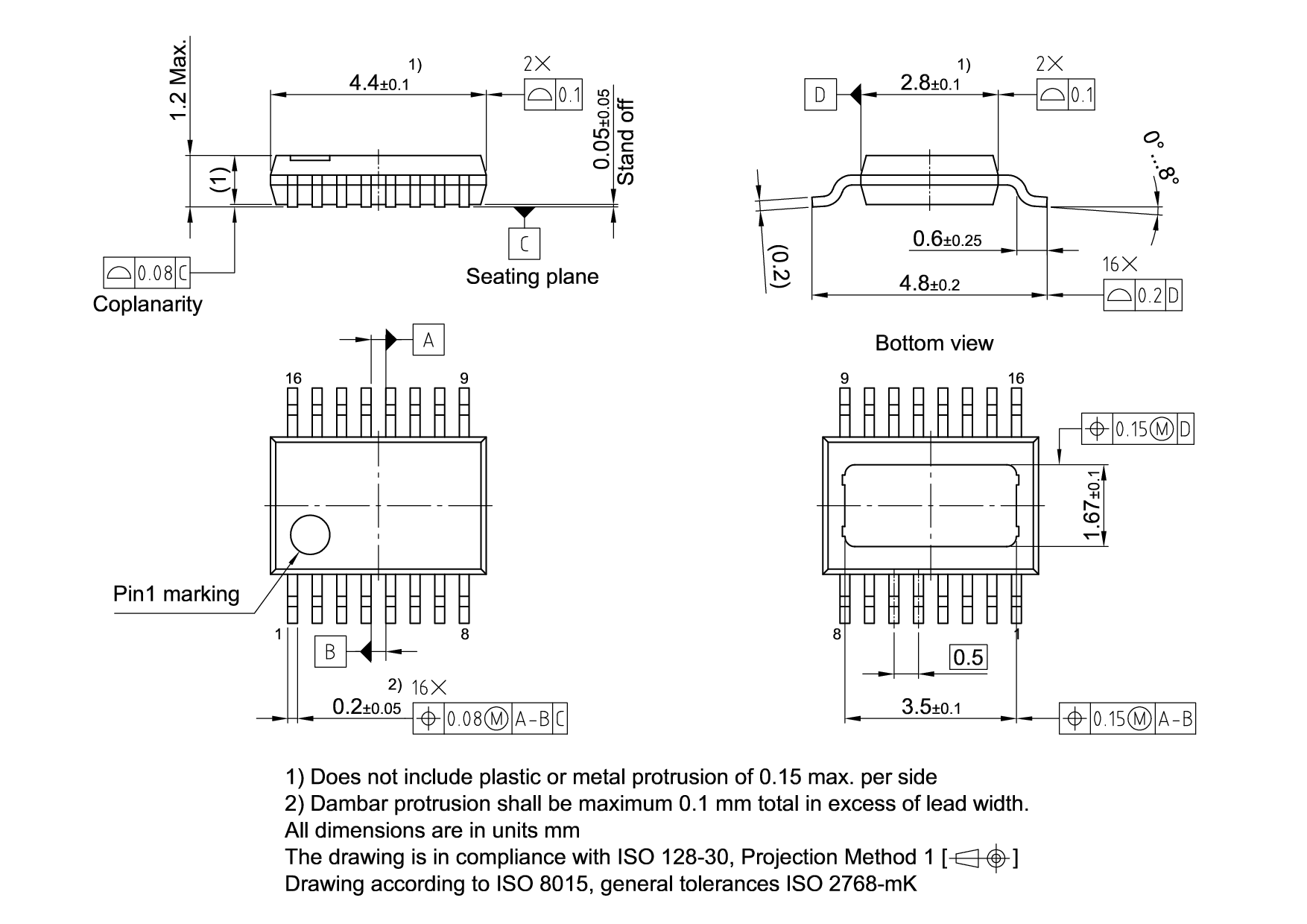
Package information
Revision history
| Document version | Date of release | Description of changes |
|---|---|---|
| Rev. 1.00 | 2024-10-14 |
|
Specified ΨJTOP is derived under natural convention conditions and provide a correlation between the junction temperature and the temperature on the package top surface. TA = 85°C. Total power dissipation = 1.5 W
Specified RthJC is simulated at natural convention on a cold plate setup (all pins and exposed pad are fixed at ambient temperature). TA = 85°C. Total power dissipation = 1.5 W
Specified RthJA1 is generated in accordance with JEDEC JESD51-3 standards at natural convection on FR4 1s0p board. The simulation has been performed on a 76.2 x 114.3 x 1.5 mm board with 70 μm, 300 mm2 cooling area. Total power dissipation 1.5W distributed statically and homogenously over all power stages
Specified RthJA2 is generated in accordance with JEDEC JESD51-5,-7 standards at natural convection on FR4 2s2p board. The simulation has been performed on a 76.2 x 114.3 x 1.5 mm board with 2 inner copper layers ( 2 x 70 μm Cu, 2 x 35 μm Cu). A total of six thermal via (∅ = 0.3 mm, plating 25 μm) is placed under the exposed pad contacting the first inner copper layer. Total power dissipation 1.5W distributed statically and homogenously over all power stages
Not subject to production test, specified by design
Not subject to production test, specified by design