PSOC™ Edge E8x2, E8x3, E8x5, E8x6 Consumer
Datasheet
PSOC™ Edge package image
Features
Compute
400 MHz Arm® Cortex®-M55 with Helium DSP, FPU, 32 KB I/D caches and 512 KB of 0-wait state SRAM tightly coupled memory
Power optimized 200 MHz Arm® Cortex®-M33 and proprietary NNLITE NPU
400 MHz Arm® Ethos-U55 NPU with 128 MACs per cycle
Memory
Up to 5 MB system SRAM to support machine learning and graphics
1 MB of SRAM coupled with the low power Arm® Cortex®-M33 CPU
512 KB of ultra low power RRAM for non-volatile storage
256 KB instruction, 256 KB data tightly coupled memory for Arm® Cortex®-M55
64 KB boot ROM
Security
Lockstep secure enclave with option to be compliant to Arm® PSA L4/Infineon Edge Protect Category 4 (EPC4) providing tamper protection, Arm® Trusted Firmware-M (TF-M) and mbedTLS libraries for cyber security regulation conformance
Cryptographic accelerators and essential security capability including protected Root-of-Trust (RoT), secure boot, secure firmware updates
PSA L4 iSE certified hardware secure enclave (certification pending)
PSA L3 certified system security (certification pending)
Human Machine Interface
2.5D GPU, display controller and MIPI-DSI interface for reducing latency and memory required to support rich graphics
2x TDM/I2S to interface to audio codec
PDM/PCM for up to 6 DMIC connections and acoustic activity detect (AAD)
Communication
11x serial communications block (SCB) with flexibility to support I 2 C, UART and SPI. 1x SCB, deep sleep capable supporting only I 2 C and SPI
High speed/full speed USB with PHY
I3C
2x serial memory interface to support external quad/octal SPI and HYPERBUS™ interface
2x SD host controller to support SD, SDIO and eMMC
Optional CAN-FD and 10/100 ethernet support
Analog
Analog front end integration with 12-bit ADC, 2x DAC, OPAMP, PGA and comparators
Autonomous operation support for I/O, analog and audio peripherals
System
Multiple power modes with integrated DC-DC buck converter; dynamic voltage and frequency management
Internal and external support for clock sources with multiple integrated PLLs
Programmable GPIO pins: drive modes, strengths, and slew rates; over-voltage tolerant (OVT) I/O programmable logic array
Power supply range: 1.8 V to 4.8 V
Ambient temperature range: -20°C to 70°C Ta
Enablement
ModusToolbox™ software ecosystem providing embedded development tools and run-time assets, including support for multiple IDE/toolchains, extensive example projects, and middleware resources
DEEPCRAFT™ Studio enabling the full journey from ML model development to embedded software
Multiple hardware development boards with integrated wireless connectivity for rapid prototyping and evaluation
Potential applications
Smart wearable
Smart lock
Description
This product line is a dual-CPU microcontroller with
a neural net companion processor,
DSP capability, high-performance memory expansion capability, low-power analog subsystem with high-performance analog-to-digital conversion and low-power comparators, IoT connectivity, communication channels, and programmable analog and digital blocks.
It also has audio and graphics blocks
.
Introduction
This product line is a high-performance, low-power MCU family, designed for compute performance, human-machine interface (HMI), machine learning (ML), enhanced sensing, real-time control, and low-power applications. Robust and easy-to-use ML and HMI software and tools are also provided.
Functions supported include security, communications and control, and DSP, in a multi-domain architecture which enables fine-grained power optimization and dynamic frequency scaling. The always‑on domain supports voice recognition, battery monitoring, and other sensing applications. These functions are provided at extremely low power.
A detailed block diagram is shown in
Figure 1
.
Device identification and revisions
Family ID = 0x115 (12‑bit); Si ID range = 0xED80‑0xEDBF, 0xF180-0xF1BF; rev ID = "0x21 (B0)"
Firmware
Revisions: Rom Boot: 2.0.0.6022, RRAM Boot: 2.0.0.7127
Figure 1.
Detailed diagram
Detailed features
This product line has the following features:
Autonomous Analog
2x Continuous-Time Blocks (CTB) offering Analog Front-End (AFE) functions such as:
Programmable Gain Amplifier (PGA)
Transimpedance Amplifier (TIA)
Pseudo-Differential Amplifier
Comparator
SAR ADC with
5 Msps sample rate at 12 bits or 250 ksps at 16 bits in System High Performance mode
200 ksps sample rate at 12 bits or 12.5 ksps at 16 bits in System Deep-Sleep mode
Accumulation and averaging – 2x, 4x, 8x … 256x
Limit detection, Offset and gain calibration
2x 12-bit DAC with 1 μS refresh time, automatic waveform generation
2x Programmable Threshold Comparators (PTComp) with post-processing supporting Audio Activity Detection (AAD) and Motor Control
Autonomous Controller capable of performing following functions in Device DeepSleep Mode
Power cycling of individual blocks
Send triggers and/or interrupts to the CPU
Digital output to as many as four GPIOs
Security features
Up to Infineon Edge Protect Category 4 (EPC 4), depending on part number (see Ordering information ) . For more information on Infineon Edge Protect, see here
Lockstep Secure Enclave in low-power always-on domain
Secure Infineon RoT key storage; secure boot
Tamper detection, side channel attack (SCA) mitigation, and protection against fault injection attacks
On EPC 4 part numbers only: Secure Enclave runtime services for Arm® Platform Security Architecture (PSA) compliant cryptography, key management, secure storage and attestation services (see Ordering information )
Off‑the‑shelf Trusted Firmware‑M enablement and Mbed‑TLS for crypto operations
Secure isolation of processing environments via Arm® TrustZone with root-of-trust established at boot by Cortex®‑M33 CPU
Factory provisioned device unique keypair (DICE_DeviceID), Hardware Unique Key (HUK), Unique Device Secret (UDS) and Infineon device certificates
Infineon proprietary protection units for memory and peripherals
Secure firmware update; secure debug, secure RMA mode for field failure analysis
Low‑power security, control, and communication CPU
Cortex®‑M33 with FPU, DSP, and MPU at 200 MHz in System High Performance (HP) power mode (see Power modes )
16‑KB I‑cache
RRAM module for NVM
DMA
Hardware crypto accelerator with comprehensive support of cryptographic algorithms
High-performance compute, DSP, and machine learning (ML) blocks
Cortex®‑M55 CPU with DSP extension at 400 MHz in System High Performance (HP) power mode (see Power modes )
FPU, MVE extension with vectored fixed and floating point
32‑KB I‑cache and 32‑KB D‑cache
256‑KB I- and 256‑KB D‑TCMs
Ethos-U55 NN coprocessor with 128 multiply-accumulate operations (MACs) per cycle; 51.2 billion operations per second
HPDMA
Multi‑AXI high‑bandwidth interconnect
Communications and connectivity
HS USB host/device, 480 Mbps
SD host controllers with eMMC mode
2x Serial memory interfaces (SMIF with 32 KB cache ) with octal DDR
Ethernet 10/100 media access control (MAC)
CAN FD
I3C bus for 2‑wire sensor hubs
I2C, SPI, and UART via serial communication blocks (SCB). SCB0 supports only I 2 C and SPI
HMI functional blocks
2.5D graphics processor for rendering images and text
Display controller with MIPI DSI
Audio: PDM microphone interface with 3 pairs of inputs, 2x TDM (Time Division Multiplexing) with 8 channels each interface, supporting I2S full and half-duplex modes
Optimizable power
Independent voltage domains allowing selectable domain power for low-power or high-performance (see Power modes )
Active, sleep, deep sleep, and hibernate modes
On‑chip DC‑DC buck converter
Dynamic frequency scaling for real‑time power optimization
Granular SRAM blocks for selectable SRAM retention
Programmable GPIO pins
Programmable drive modes, strengths, and slew rates
Over‑voltage tolerant (OVT) pins for I 2 C compliance
RTC with 16 backup registers
ModusToolbox™ design environment
Code development and debugging in a cross-OS (Windows, Linux, Mac OS) IDE-neutral environment supporting Visual Studio Code, IAR, Keil and Eclipse IDEs
Installable software development kits (SDK) for peripheral initialization, clock and pin configuration, and middleware selection
Peripheral driver library (PDL) for peripheral APIs, including SD host controller for connection to IoT devices; and ML library
Industry-standard CMSIS pack support
RTOS support, including FreeRTOS
DEEPCRAFT™ Studio enabling the full journey from ML model development to embedded software
Development ecosystem
PSOC™ Edge MCU resources
A wealth of data available at www.infineon.com helps you to select the right PSOC™ MCU and quickly and effectively integrate it into your design. The following is an abbreviated list of resources for PSOC™ Edge E8 MCU.
Overview : PSOC™ portfolio
PSOC™ Edge E8x2, E8x3, E8x5, E8x6 Architecture Reference Manual : This document contains architectural descriptions of hardware blocks
PSOC™ Edge E8x2, E8x3, E8x5, E8x6 Registers Reference Manual : This document contains a list of registers and bit‑fields in the hardware blocks
Application notes
cover a broad range of topics, from basic to advanced level, and include the following:
AN235935 : Getting started with PSOC™ Edge E84 on ModusToolbox™ software
AN239191 : Getting started with graphics on PSOC™ Edge MCU
AN236697 : Getting started with PSOC™ MCU and AIROC™ connectivity devices
AN237849 : Getting started with PSOC™ Edge security
AN240096 : Getting started with Trusted Firmware-M (TF-M) on PSOC™ Edge
AN236282 : Device Firmware Update (DFU) Middleware (MW) for ModusToolbox™
AN238041 : PSOC™ Edge provisioning specification
AN236517 : PCB layout guidelines for PSOC™ Edge E84 MCU
AN237976 : PSOC™ Edge E84 MCU low-power modes and power reduction techniques
AN239774 : Selecting and configuring memories for power and performance in PSOC™ Edge MCU
AN237816 : PSOC™ Edge E84 MCU voice and audio firmware components guide
AN239757 : Authenticated debug for PSOC™ Edge
AN240857 : PSOC™ Edge MCU Lifetime Estimate
Code Examples : Numerous example applications featuring various peripherals and system middleware are available on Infineon GitHub repositories
Development kits including documentation, schematics and layout files
General purpose evaluation kit: KIT_PSE84_EVAL
Artificial Intelligence/Machine Learning kit: KIT_PSE84_AI
Training
- PSOC™ Edge lab-based training modules
Video training on Infineon products and tools
Technical Support : PSOC™ development community forum , Knowledge base articles , My cases
ModusToolbox™ software
ModusToolbox™ Software is Infineon’s comprehensive collection of multi-platform tools and software libraries that enable an immersive development experience for creating converged MCU and wireless systems. It is:
Comprehensive - it has the resources you need
Flexible - you can use the resources in your own work flow
Atomic - you can get just the resources you want
Infineon provides a large collection of code repositories on GitHub. This includes:
Board support packages (BSPs) aligned with Infineon kits
Peripheral driver library (PDL) provides the low-level, device-specific firmware drivers for accessing the hardware sub-systems and peripherals
Middleware enabling industry-leading features such as CAPSENSE™, Bluetooth® Low Energy, and mesh networks. Additionally, a Hardware abstraction layer (HAL) provides middleware portability across product families
An extensive set of thoroughly tested code example applications
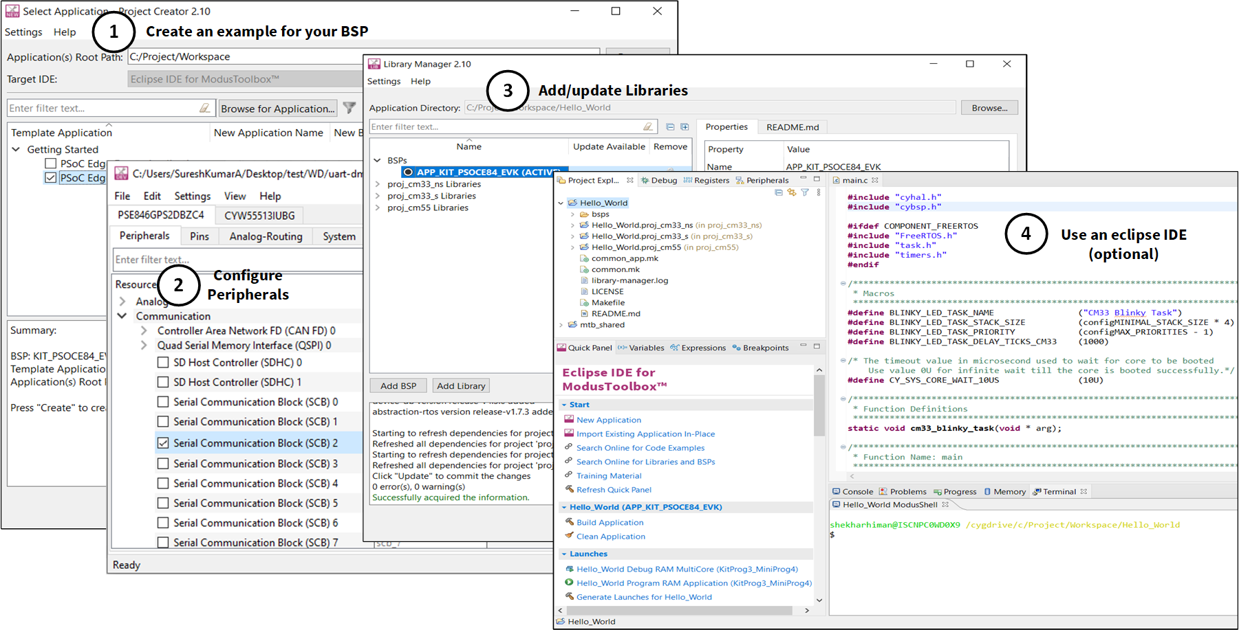
ModusToolbox™ software is IDE-neutral and easily adaptable to your workflow and preferred development environment. It supports Windows, Linux, MacOS, IAR, Keil, and Visual Studio Code. As
Figure 2
shows, it includes (1) a project creator, (2) peripheral and library configurators, (3) a library manager, and (4) an optional Eclipse IDE for ModusToolbox™.
For information on using Infineon tools, refer to the documentation delivered with ModusToolbox™ software, and AN235935 – Getting started with PSOC™ Edge E84 on ModusToolbox™ software.
Figure 2.
ModusToolbox™ Software Tools
Chip-level functional description
Power
This product line offers multiple features for managing and reducing power draw. Multiple power modes include active, sleep, deep sleep, and hibernate. Deep sleep has three variations based on retention of SRAM.
The power control block provides assurance that voltage levels meet the requirements of the respective modes. It can:
Delay mode entry (for example, at power‑on reset (POR)) until voltage levels are as required for proper functioning
Detect operation below safe power supply levels:
Generates interrupts for low-voltage detection (LVD)
Generates reset for brownout detection (BOD)
This product line operates with a single 1.8 V ±5% regulated supply, or from a 2.7 to 4.8 V supply along with a 1.8 V 5% regulated supply. The core logic can operate at different levels with a trade-off in performance and power. In conjunction with clock gating at peripheral and bus levels, this permits fine-grained optimization of energy usage.
A buck regulator powers the core logic at three levels: 0.7 V, 0.8 V, and 0.9 V; (see
Power modes
). The buck efficiency is ≥80% in the active power mode. The buck configuration is single in, single out (SISO).
Dynamic voltage and frequency scaling are supported. Voltage level switching is implemented by writing to power control registers.
Power connections
The following power system diagrams show typical connections for power pins for all supported packages. In these diagrams, the package pin is shown with the pin name, for example "VDDQ , A11". For VDDIOx pins, the I/O port that is powered by that pin is also shown, for example "VDDIO1; E6,; I/O port P8".
The diagrams show two ways to power the device:
Supply powered: All VDDx pins are tied to 1.8 V. Isolated sources can be used, for example to isolate analog circuits or to isolate the rest of the system from noisy GPIOs. All "VBAT" related pins are grounded.
Battery powered: VBAT is connected to a supply ranging from 2.7 V to 4.8 V. Other VDDx pins must still be connected to 1.8 V. All "1P8" pins are grounded.
Note that the smaller packages do not have a VBAT pin; these packages can only be supply powered.
In both cases, VDD.USB is tied to 3.3 V if USB is being used. If not, should be tied to ground.
When none of the ports associated with VDDIOx are in use, except for VDDIO7, tie all remaining VDDIOx pins to ground and VDDIO7 to 1.8 V, as it has the power detect circuit for all IOs in the chip.
There is no dependency on power supply sequencing. See
System Resource
; they apply to both power-up and power-down.
The bypass capacitors shown in the following diagrams are recommendations for typical use only. Actual bypass capacitor usage and size depend on the application.
Figure 3.
BGA-220 package, supply powered
Figure 4.
BGA-220 package, battery powered
Figure 5.
eWLB-235 package, supply powered
Figure 6.
eWLB-235 package, battery powered
Figure 7.
WLB-154 package, supply powered
Power distribution and domains
This product line has independent voltage domains, allowing domain power to be for low-power or high-performance (see Power modes ).
Diagrams of power distribution are shown in
Figure 8
through
Figure 10
.
Figure 8.
Power distribution, supply powered
Figure 9.
Power distribution, battery powered
Figure 10.
Power distribution to internal blocks
In a typical use case:
The low-power domain is never switched off unless chip power is cut off, and
The high-performance domain is used for high-speed communication channels ( >100 MHz, display controller outputting frames via MIPI DSI), and DSP and neural network processing, where work is done as fast as possible to reduce real time constraints for applications. Additionally, the high-performance domain can be selectively powered down to save energy and reactivated when needed, while the low-power domain continues to remain active.
The low and high power domains are powered by the same buck converter output — all power domains operate at the same voltage domain.
Power modes
This product line can operate in five system and three CPU power modes. These modes are intended to minimize the average power consumption in an application.
Power modes supported are:
System High Performance (HP): All peripherals and CPU power modes are available at maximum speed. Core logic runs at 0.9 V.
System Low Power (LP): All peripherals and CPU power modes are available at reduced speed. Core logic runs at 0.8 V.
System Ultra-Low Power(ULP): All peripherals and CPU power modes are available at minimal speed. Core logic runs at 0.7 V.
CPU Active: CPU executes code in system
HP, LP, or ULP
mode.
CPU Sleep: CPU code execution is halted — the CPU clock is gated off — in system
HP, LP, or ULP
mode.
CPU Deep Sleep: Same as CPU Sleep; in addition the CPU's System Deep Sleep request signal is activated.
System Deep Sleep: Only Deep Sleep-capable peripherals are available after both CPUs enter CPU Deep Sleep mode. This mode has two sub-modes: System Deep Sleep RAM and System Deep Sleep Off. See
Table 1
for details.
The device transitions to System Deep Sleep mode only when either of the following conditions are met:
Both CPUs are in Deep Sleep mode
The high-performance domain is powered OFF, and the Cortex®‑M33 is in Deep Sleep mode
System Hibernate:
This is the lowest current mode. Almost all functionality is powered off in this mode except for the RTC, watchdog timer (WDT), and low-power comparators (LPCOMP), along with the ability to wake up on activity on a limited set of pins and retaining limited application data using backup registers. Wakeup is tantamount to a cold boot. GPIO states are retained in this mode.
CPU Active, Sleep, and Deep Sleep are standard Arm® defined power modes supported by the Arm® CPU instruction set architecture (ISA). System HP, LP,
ULP,
Deep Sleep and Hibernate modes are additional power modes provided by the device.
Power mode transitions
This product line generally supports Arm® standard power modes; see
Power modes
for details. Table 1 lists the supported power modes.
CPU Active/Sleep | System Deep Sleep | System Deep Sleep-RAM | System Deep Sleep-Off | System Hibernate | Off | |
|---|---|---|---|---|---|---|
Parameters | ||||||
Wake source | Any interrupt | DS peripherals | DS peripherals | DS peripherals | RTC/HIB peripherals | Power on |
Wake action | Resume | Resume | Warm boot | Reset/cold boot | Reset | Reset |
Wake time | One CPU cycle | < 20 μs | Deep sleep+warm boot | Deep sleep+cold boot | POR+coldboot; < 1 ms | |
Resources | ||||||
IHO | On | Off | Off | Off | Off | Off |
PILO | On/Off | On/Off | On/Off | On/Off | On/Off | Off |
ECO | On/Off | On/Off | On/Off | On/Off | Off | Off |
WCO | On/Off | On/Off | On/Off | On/Off | On/Off | Off |
CPU | On/Sleep | retention | Off | Off | Off | Off |
SRAM | On/select off | Off/select retention | Off/select retention | Off | Off | Off |
Power block support
shows the available operational states for the major blocks in this product line. Note that operational states possible in low-power modes are generally limited in functionality and parametric performance as compared to their capabilities in the active modes. Also, blocks that do not support low power modes such as System Deep Sleep and System Hibernate cannot wake up the CPUs from these modes. See
Power modes
for details.
Block | Power mode | |||
|---|---|---|---|---|
CPU Active | CPU Sleep | System Deep Sleep | System Hibernate | |
CPU subsystem | ||||
CPUs | Y | N | N | N |
NPUs | Y | Y | N | N |
NVIC | Y | Y | N | N |
WIC | Y | Y | Y | Y |
RRAM | Y | Y | N | N |
SRAM | Y | Y | Programmable | N |
DMA | Y | Y | N | N |
Programmable digital | ||||
Smart I/O | Y | Y | Y | N |
Fixed-function digital | ||||
TCPWM | Y | Y | N | N |
SCB | Y | Y | N, SCB0 is supported in System Deep Sleep power mode | N |
SMIF | Y | Y | N | N |
SD host controller | Y | Y | N | N |
USB | Y | Y | N | N |
CAN FD | Y | Y | N | N |
Ethernet | Y | Y | N | N |
I3C | Y | Y | N | N |
MIPI-DSI | Y | Y | N | N |
TDM/I2S | Y | Y | N | N |
PDM | Y | Y | N | N |
Crypto | Y | Y | N | N |
Special function | ||||
Graphics subsystem | Y | Y | N | N |
Programmable analog | ||||
LPComp | Y | Y | Y | Y |
SAR ADC | Y | Y | Y (duty cycled) | N |
DAC | Y | Y | Y | N |
PTComp | Y | Y | Y | N |
CTB | Y | Y | Y | N |
IO | ||||
GPIO | Y | Y | Y | Y |
System resources | ||||
WDT | Y | Y | Y | Y |
MCWDT | Y | Y | Y | N |
RTC | Y | Y | Y | Y |
Backup registers | Y | Y | Y | Y |
OVD | Y | Y | N | N |
LVD | Y | Y | N | N |
Security
This product line includes a Cortex®‑M55 and an Arm® TrustZone enabled Cortex®‑M33 CPU. It provides an isolated fully secure hardware-based Root-of-Trust (RoT) that supports secure boot, secure provisioning, and secure debugging. This RoT is initially owned by Infineon and is extended to the user or OEM during the provisioning process. Provisioning installs the OEM keys; debug, boot, and system configuration policies; and extended boot.
Secure and non-secure debug access is supported; in non-secure access, areas marked "secure" are not accessible by the debugger. In the most secure case provided, the device can be “locked” such that it may not be acquired for test/debug.
Certificate management assures appropriate accesses are provided at different stages of development and production.
This product line is fully compliant with Arm® TrustZone at hardware and software levels. An extra layer of security is implemented with the help of Infineon-proprietary protection units.
For EPC 4 part numbers only (see
Ordering information
): secure enclave runtime services provide access to PSA compliant cryptographic services, key management, attestation, and secure storage services.
Security features
Infineon Edge Protect Category 2 (EPC 2) supporting SESIP/PSA level 2 or Edge Protect Category 4 (EPC 4) supporting SESIP/PSA level 3 + secure enclave, depending on part number (see Ordering information )
Exclusive access to 5120 bytes of OTP memory for storage of security assets (seeNonvolatile memory )
Hardware crypto accelerator with comprehensive support of cryptographic algorithms
Secure isolation of processing environments via Arm® TrustZone
Infineon proprietary MPU, MPC and PPCs for memory and peripheral access control
Lock‑step secure enclave with the following features:
Secure boot with hardware-based root of trust (RoT) enabled
Device identifier composition engine (DICE) mechanisms for device attestation
Cryptography services
EPC 4 part numbers only (see Ordering information ): secure enclave runtime services
Tamper detection, side channel attack (SCA) mitigation, and protection against fault injection attacks
Off‑the‑shelf secure isolation using Trusted Firmware‑M (TF‑M); and mbedTLS crypto acceleration package
For more information on EPC2 and EPC4, refer to
Infineon Edge Protect
.
Security architecture overview
This product line has an isolated secure enclave and two CPUs: Cortex®‑M33, and Cortex®‑M55; as
Figure 11
shows:
Figure 11.
Security architecture diagram
Secure enclave:
Provides secure boot process including root of trust (RoT) and DICE mechanisms. Boot starts from ROM_BOOT stored in local ROM
Provides local crypto block for secure cryptographic operations, including SCA and DPA protected crypto
Provides run-time services to support secure boot, secure firmware update, and other RoT services
Supports lockstep architecture with two islands of replication for CPU (2x) and crypto (2x), for protection against fault attacks and semi-invasive attacks inside the CPU
Cortex®‑M33:
Arm® TrustZone enabled core with two processing environments: secure (SPE) and non‑secure (NSPE)
Infineon proprietary protection units for memory and peripheral protection
Integrated mbedTLS crypto acceleration package that supports software and hardware cryptography services
Infineon-provided Trusted firmware‑M (TF‑M) implemented in SPE — its services are leveraged by Cortex®‑M33 NSPE and Cortex®‑M55, fully enabled to use hardware accelerated crypto operations
Cortex®‑M55:
This is an application core operating in NSPE. Applications run by this CPU can request TF‑M services using PSA API calls
Block functional description
Processors
This product line has a multiple CPU architecture:
Arm® Cortex®‑M55, running at up to
400
MHz
A machine learning (ML) coprocessor with the Cortex®‑M55 CPU: the Arm® Ethos-U55 CPU, running at the same clock frequency as the U55
Arm® Cortex®‑M33 CPU, running at up to
200
MHz
A neural network (
NNLite
) coprocessor with the Cortex®‑M33 CPU, running at the same clock frequency as the M33
An inter-processor communication (IPC) block is included for synchronizing the CPUs' tasks.
The M33 CPU has Floating Point Unit (FPU), Digital Signal Processor (DSP), and Memory Protection Unit (MPU). It has Arm® TrustZone technology, and provides secure boot and secure zone settings. The M55 CPU has FPU with vectored fixed and floating point, and Arm® M-Profile Vector Extension (MVE).
The M33 CPU domain is a low-power domain. The M55 domain is a high-performance domain for high-performance compute purposes. The CPUs can access resources in each others' domains via a bus bridge.
Both CPUs have single-cycle cache memories to increase performance and reduce power. The M33 CPU has a 16-KB 4-way set associative I‑cache. The M55 CPU has 32-KB I- and D-caches with the same cache architecture.
M55 TCM sizes are 256 KB each (I and D).
Each CPU has an Arm® Nested Vectored Interrupt Controller (NVIC) and an Arm® Wakeup Interrupt Controller (WIC). A WIC can wake up its processor from its CPU Deep Sleep mode. See
Power modes
for details.
Both CPUs have debug interfaces and support both SWD and JTAG. The chip also supports boundary scan for testing on a PCB; a separate TAP controller is provided for controlling boundary scan functions.
Both CPUs have trace capability. The M55 and M33 are connected to an Arm® Embedded Trace Macrocell (ETM) which is connected to an Arm® Trace Port Interface Unit (TPIU) with a standard ETM interface. The M33 CPU supports instruction trace with an Arm® Micro Trace Buffer (MTB) with 8-KB trace SRAM. Maximum trace clock frequency is 200 MHz, allowing CPUCLK/2 tracing.
shows the maximum operating frequency of each set of CPU for each of the system power modes (see
Power modes
).
System power mode | M55 /U55 | M33/ NNLite |
|---|---|---|
High Performance (HP) | 400 MHz | 200 MHz |
Low Power (LP) | 140 MHz | 80 MHz |
Ultra-Low Power (ULP) | 50 MHz | 50 MHz |
Inter-Processor Communication (IPC)
In addition to the Arm® SEV and WFE instructions, this product line incorporates two Inter-Processor Communication (IPC) blocks, namely IPC0 in the low-power domain and IPC1 in the high-performance domain. IPCs are not system deep sleep capable; however, IPC can wake up other CPUs from deep sleep. IPC0 can wakeup the high-performance CPU subsystem, whereas IPC1 can wake up the low-power CPU subsystem from CPU deep sleep. Each IPC instance includes 16 channels and 8 interrupt structures. The IPC channels can be used for communication and synchronization between CPUs. Each IPC channel also implements a locking scheme that can be used to manage shared resources. The IPC interrupts let one CPU interrupt the other, signaling an event. This is used to trigger events such as
Notify
and
Release
of the corresponding IPC channels. IPC0 channels 0 and 1 are reserved for the secure enclave.
DMA
The high performance and low power domains each include a DMA controller that can be used to transfer data to and from memory, peripherals, and registers. This allows for autonomous, deterministic control of peripherals such as the PWM, or enables large data transfers from a peripheral such as the ADC to memory.
There are two distinct DMA types, the HPDMA (AXI DMAC) and the DMA. The HPDMA and DMA are differentiated by their performance and their usage. The DMA controllers are bus masters in their respective domains:
High Performance Domain: A high-performance DMA (HPDMA) with 4 channels. Each channel has a 128-byte FIFO and its own transfer engine that arbitrates for bus master access. The HPDMA uses the 64‑bit AXI bus that shares a clock with the high performance CPU. The HPDMA is typically used to transfer large amounts of data.
Low Power Domain: Two DMA controllers with 16 channels each. The two transfer engines independently request and utilize 16 channels each, arbitrating for bus master control as needed. This DMA uses the 32‑bit AHB bus that shares a clock with the low power CPU. The DMA is optimal for small data size, transactional DMA, which would typically be used to transfer bytes between peripherals such as from ADC to RAM.
Cryptographic accelerator (CRYPTO)
This subsystem is a hardware implementation for acceleration of cryptographic functions and random number generators. It is accessible by Cortex®‑M33 and Cortex®‑M55 CPUs.
The cryptographic accelerator implements hardware support for the following:
True random number generator (TRNG) and pseudo-random number generator (PRNG)
CRC, up to 32 bits
Symmetric algorithms and key lengths
AES (128/192/256), triple DES (112/168)
CHACHA20 stream cipher
Asymmetric algorithms, key lengths, and curves
Elliptic curve cryptography (ECDSA) and RSA
ECC curves: 224, 256, 384, 521
RSA key length: 1024, 2048, 4096
Vector unit for acceleration of asymmetric key cryptography
Hashes: SHA2 (256/384/512), SHA3 (256/384/512)
Memory
This product line has a variety of volatile and nonvolatile memory types, including access to external memory ICs (see
Serial Memory Interface (SMIF)
). All CPUs and other bus masters can access any memory block. The number of wait states depends on the access path, see
Wait states and latencies
.
Nonvolatile memory
This product line has 512 KB of nonvolatile resistive random access memory (RRAM) in the low power domain. Read access time is 35 ns. RRAM is read 128 bits at a time; with word caching. There are also 25 bits for ECC. Write access is one bit at a time, at approximately 1 µs/bit.
5120 bytes of RRAM are dedicated to OTP use cases, including storage of security assets (see
Security features
).
For detailed memory map of the RRAM, refer RRAM regions section in
PSOC™ Edge E8x2, E8x3, E8x5, E8x6 architecture reference manual
.
Parameter | Conditions | Minimum |
|---|---|---|
RRAM endurance | -20 to +70 °C ambient | 100k write cycles |
RRAM retention | Ta ≤ 70 °C, 100k P/E cycles | 20 years |
EEPROM
In this product line, part of the RRAM may be used to emulate EEPROM using the supplied software driver. The implementation uses redundancy (an integer multiple of the EEPROM memory size) for simplicity. The EEPROM-like memory has the following properties:
Byte-programmable
Size selectable from 1 KB to 64 KB in binary increments
1 million cycles endurance at 25 °C, 200k cycles over -40 to +85 °C with 20-year life
SRAM
This product line has SRAM and system SRAM, in the low-power and high-performance domains:
SRAM: 1 MB in the low power CPU subsystem (Cortex®‑M33). Portions of this SRAM can be retained during the System Deep Sleep power mode; the retained amount is selectable in 64‑KB increments. The SRAM is implemented as several independent blocks to allow simultaneous access from different processors to different regions.
System SRAM ("SoCMEM"): 5120 KB in the high-performance domain. This memory is organized in
ten
partitions of 512‑KB each, with retention of individual partitions. It can be accessed from either the M55 or the M33, with bus arbitration.
Serial Memory Interface (SMIF)
This product line features two SMIF interfaces,
each equipped with a 32 KB cache
, depending on the package
(see
Table 9
and
Ordering information
)
. Each interface can access up to 1 GB of address space allocated in the memory map.
The SMIF allows code execution-in-place (XIP) from the external memory; it is not required to copy code into the internal memory to execute it. Up to 64 MB is supported in XIP mode.
On-the-fly (OTF) encryption and decryption are supported. The SMIF supports a clock speed of 200 MHz in octal xSPI DDR mode. Infineon HYPERBUS™ is also supported.
Wait states and latencies
When accessing a memory area from the CPU, specifically the CM33 or CM55 cores, the primary focus is on the time required to retrieve data (read) at the relevant system operating frequencies. While write access times are also relevant, writes can typically be posted, allowing the operation to proceed without requiring immediate acknowledgment. In contrast, reads must traverse the full outbound address and control signal path, as well as the inbound data access path, which directly affects system performance and response times. It is important to note that this section is limited to scenarios where the CPU is the bus master, and other potential bus masters in the system are not the focus of this analysis.
Generally, there are two components in the access time:
Wait states of the memories being read
Delay through the Network Inter-Connect (NIC)
This section covers wait states for RRAM and SRAMs, which are of primary interest to users.
Wait states (WS):
RRAM: RRAM writes are much slower than RRAM reads (as it is typical for most non-volatile memory) and are not considered here.
RRAM read is controlled by an internal 160 MHz read state machine clock, which is designed to produce data in 30 ns (also referred to as “analog read time") irrespective of the voltage mode (0.7 to 0.9 V). Besides this time, the following times are required for an RRAM read: 1 clock for address read and 1 clock for ECC correction (assuming 0 or 1 bit correction; otherwise, it will be longer).
Based on 30 ns, the WS values for a cycle time of Tcyc in nanoseconds will be ceil (30/Tcyc). For example, for a 200 MHz AHB clock frequency, the WS value will be 6; for 50 MHz, it will be 2.
Voltage (V)
Frequency (MHz)
Wait states (WS)
0.9 (HP mode)
200
6
0.8 (LP mode)
80
3
0.7 (ULP mode)
50
2
SRAM: All SRAMs are designed to have zero wait states at their peak target frequencies. This is the time for SRAM to deliver data, meaning that the address is latched on one clock edge and data is available on the next edge.
Access cycles do not change with voltage and frequency scaling so that provided voltage and frequency limits are observed; all SRAM wait states remain zero wait states. This implies that the number of cycles to access SRAM (CLK_HF0) and system SRAM (CLK_HF2) do not change.
Delay through the Network Interconnect (NIC):
M33:
Memory resource
Outbound clock cycles
Access time
Inbound clock cycles
Comment
RRAM
3 AHB clocks
Ceil(30ns/AHB Tcyc)
2 AHB clocks
128-bit C-AHB. I-Cache refill. 32-bit access is similar
SRAM
- - 1 AHB clock
No wait states
System SRAM
3 AHB clocks
6 System SRAM clocks
2 AHB clocks
32-bit access and 128-bit access (parallel bank read)
M55:
Memory resource
Outbound clock cycles
Access time
Inbound clock cycles
Comment
RRAM
3 AXI + 5 AHB cycles
2 * Ceil (30ns/AHB Tcyc)
4 AHB + 4 AXI cycles
64-bit word read takes 2 cycles
SRAM
3 AXI clocks + 3 AHB clocks
4 AHB cycles (2 accesses)
7 AXI clocks + 3 AHB clocks
64-bit word read takes 2 cycles
System SRAM
3 AXI clocks
6 System SRAM clocks
2 AXI clocks
First word access, subsequent accesses each take one System SRAM clock
Protection units
Protection units are hardware blocks that implement schemes to protect memory, peripherals and shared resources from bus masters, preventing unauthorized code from accessing those resources. This product line has multiple protection units. Implementation Defined Attribution Unit (IDAU), Secure Attribution Unit (SAU) and Memory Protection Unit (MPU) are part of Arm® TrustZone technology; in addition Infineon provides proprietary protection units such as MPCs and PPCs.
The MPCs and PPCs use the concept of secured and non-secured address aliases. They use the aliases to control the accessibility of memory regions and peripherals, to make them secured or non-secured. They also isolate memory regions and peripherals from CPU masters by means of protection contexts.
Protection context (PC)
is a pseudo state of a bus master, controlled with a set of hardware registers that configure each bus master with certain attributes, which the protection units use to determine access. The protection units support memory and peripheral access attributes including address range, read/write, code/data, privilege level, secured/non-secured, as well as protection context. For example, PCs can be set up to isolate a memory region or peripheral such that it is accessible by a single CPU, and not accessible by the other CPU.
This product line supports up to eight protection contexts. Some protection unit resources and protection contexts are reserved for system usage, see the reference manual for details.
Clocks
This product line has fully integrated clocks. It provides clocks to all blocks that require clocks. It switches between different clock sources without glitches, and ensures that no metastable conditions occur.
The clock sources are:
Internal high-speed oscillator (IHO): 50 MHz ±1%
Precision internal low-speed oscillator (PILO): 32 kHz, no external crystal needed. Periodic calibration can be done by software (driver / library supplied).
External crystal oscillators (ECO and WCO)
Three digital phase-locked loops (DPLL) are available for clock generation. They operate in the System
HP, LP, and ULP
power modes (see
Power modes
).
External clock input
The DPLLs provide fast wake‑up at high clock speeds. DPLL jitter levels are low and allow 12-bit SAR ADC operation. There are two types of DPLL:
Two lower frequency and optimized for low power (DPLL LP)
One high-frequency and high-performance (DPLL HP)
The HP DPLL is optimized for high‑speed operation. It works over a broad range of frequencies, i.e., 50 MHz to
500 MHz
. The LP DPLL operating range is
10
MHz to
500
MHz
Clocks can be divided down to generate synchronous clocks for the analog and digital peripherals. Integer and fractional clock dividers are provided:
Eight 8‑bit clock dividers
Sixteen 16‑bit integer clock dividers
Four 16.5 fractional clock dividers
One 24.5 fractional clock divider
The 16‑bit dividers allow more flexibility in generating fine-grained frequency values. The digital clock dividers generate either 1 in N clocking where N = divisor or an approximately 50% duty cycle clock for the analog circuitry.
Internal high-speed oscillator (IHO)
The IHO operates at a fixed 50 MHz frequency. Its tolerance is ±1%. A high-speed clock can be derived using the IHO plus a DPLL. The IHO is used as the clock source during wakeup.
Precision internal low-speed oscillator (PILO)
The PILO is a precision low-power oscillator with a typical current of 1.15 µA and frequency of 32.768 kHz with 250 ppm accuracy. The PILO can operate in the System Hibernate power mode.
Watchdog timer (WDT)
This product line has one free-running watchdog timer (WDT) and
two
multi-counter watchdog timers (MCWDT). Both WDTs generate device reset if not serviced within a configurable interval. In addition, the WDTs can be used as an interrupt source or a wakeup source in low-power modes (MCWDT is recommended for this use case). The Free-running WDT can be clocked by PILO and is available in all device power modes. MCWDT can be clocked by PILO or WCO and is available in all except Hibernate power-mode.
External crystal oscillators (ECO)
This product line has two oscillators that use external crystals: high-frequency and low-frequency (watch crystal). Both oscillators can be used in precision timing applications. The WCO is low-power and has a frequency tolerance of 250 ppm.
shows all of the external crystal oscillator circuits for this product line. The component values shown are typical; check crystal datasheet for the load capacitor values.
Figure 12.
External Oscillator Circuits
Rs is key to limiting power delivered to XTAL/resonator so that it does not get damaged. It also contributes to phase shift of the overall network.
Following are the recommended crystal specifications:
ECO
Nominal frequency: 4 to 35 MHz
Drive level protection: 100 ~ 200 μW at minimum
Equivalent Series Resistance (ESR): Upto 200 Ω for oscillation
Crystal load capacitance (C
L
): 10 pF
WCO
Nominal frequency: 32.768 kHz
Drive level protection: 0.1 ~ 0.5 μW
Equivalent Series Resistance (ESR): Upto 90 kΩ for oscillation
Crystal load capacitance (C
L
): 4 pF to 14 pF (5% tolerance)
Typical current of 120 nA @ 4 pF load
For more information, see the
PSOC™ Edge E8x2, E8x3, E8x5, E8x6 architecture reference manual
and
AN236503
PSOC™ E8 MCU hardware design considerations.
Real time clock
This product line includes a real time clock (RTC). The RTC has the following features:
Binary values for time (hour, minute, and second fields), date (day, month, and year fields), and day of week
12‑hour or 24‑hour format
Automatic leap year correction with century interrupt
Sixteen 32-bit backup registers to retain application data in all low-power modes, including Deep Sleep-OFF and Hibernate mode
In addition to the above features, the RTC has two individual alarms with matching for six RTC fields (hour, minute, second, date/month, and day of week). Both alarms have interrupts to notify matching; these interrupts can wake up the system.
Reset
This product line is reset from a variety of sources including a software reset (SRES). Reset events are asynchronous and guarantee reversion to a known state. The reset cause is recorded in a register, which retains its state through reset and allows software to determine the cause of the reset. An XRES pin is reserved for external reset input.
The XRES pin is active low. It should be externally pulled up to V
DDD
via a 4.7 kΩ resistor as shown in
Figure 10
. This will make sure that the XRES pin is not left floating in the design and that the device can function properly. It is recommended to connect a capacitor (typically 0.1 µF) to the XRES pin to filter out glitches and give the reset signal better noise immunity. Optionally, if the device is controlled by an external host, the XRES pin can be directly driven by the host.
Figure 13.
XRES Connection Diagram
Autonomous Analog
Autonomous Analog is a low-power, reconfigurable, mixed-signal, sensing, conditioning, and response system that operates independently of the CPU.
Figure 14.
Autonomous Analog block diagram
The run-time control activities, such as enabling or disabling blocks, changing the power modes of the blocks, switching inputs/routing, waiting for the ADC scan to finish, triggering the DAC, and so on, are done by the Always-On Autonomous Controller independent of the CPU. For this purpose, most analog blocks in Autonomous Analog have a static configuration (unchanged by the Autonomous Controller during run-time) and a Dynamic Configuration (can be changed by the Autonomous Controller during run-time).
SAR ADC
Autonomous analog in this product line has a SAR ADC with the following features:
12- to 20-bit (with accumulation) results
5-Msps sample rate at 12 bits or 250-ksps at 16 bits in System High Performance mode (HS mode ADC)
200-ksps sample rate at 12 bits or 12.5-ksps at 16 bits in System Deep Sleep mode (LP mode ADC)
Buffered Inputs
Inputs from 16 pins or 7 internal signals (from opamps, DACs, temperature sensor etc.)
Simultaneous sampling of as many as 10 inputs
32 logical channels
Post processing and storage
Accumulation and averaging – 2x,4x, 8x … 256x
Two 64-tap FIR filters
A 512-entry FIFO that can be subdivided into 2, 4, or 8 FIFOs
Limit detection
Offset and gain calibration
DAC
Autonomous Analog in this product line has two digital-to-analog converters (DACs) with the following features:
12-bit continuous time output
1-µs settling time
Waveform generation using a 512-entry waveform data memory
Buffers with sample and hold support
16 input channels (15 hardware and 1 firmware)
Selectable voltage reference:
VDDA
VDDA/2
Internal 0.9-V band-gap reference
External VREF buffered through CTB opamps
Continuous time block (CTB)
Continuous-Time Blocks (CTB) consist of opamp circuits that can perform analog front-end functions.
Autonomous-Analog in this product line has two CTBs, each consisting of two opamps, feedback resistor networks, and multiplexers that can form topologies such as:
Programmable Gain Amplifier (PGA)
Trans-impedance Amplifier (TIA)
Pseudo-Differential Amplifier
Unity Gain Buffer (Voltage Follower)
Open Loop Opamp
Comparator
PTComp
Programmable-Threshold Comparators (PTComp) are used to compare an input with another input or a reference.
Autonomous analog in this product line has two PTComps with the following features:
Programmable power and response times
Selectable inputs from as many as 16 GPIOs and eight internal signals
A 30-mV hysteresis option
Rising edge, falling edge, and combined rising and falling edge detection at the comparator output
Post-processing to detect comparator activity - used for applications such as acoustic activity detect and Motor Control
Low-power comparator
This product line has two low-power comparators, which operate in System DeepSleep and System Hibernate power modes. This allows other analog blocks to be disabled while retaining the ability to monitor external voltage levels during low-power modes. The comparator outputs are synchronized to avoid metastability, unless operating in an asynchronous power mode (that is, System Hibernate) where the wake-up circuit is activated by a comparator switch event.
Fixed function digital
Timer/counter/PWM (TCPWM)
This product line has 32 TCPWM blocks. Eight have 32‑bit counters and 24 have 16‑bit counters.
Each TCPWM block consists of the following:
a counter
a period register to either stop or auto-reload the counter
a capture register to record the counter value at the time of an event
compare registers to control PWM duty cycle
Edge-aligned, center-aligned, and asymmetric-aligned PWM
PWM true and complementary outputs with a programmable offset to create a dead-band between the outputs
PWM kill input; can be driven by an external voltage level via a comparator
Quadrature input measurement
Serial communication block (SCB)
This product line has 12 SCBs
(9 in the WLB-154 package, see
Ordering information
)
. SCB1 to SCB11 can be configured to implement an I2C, UART, or SPI interface, and can be masters or slaves. SCB0
can operate in the System Deep Sleep power mode with an external clock; and it only supports I2C slave mode and SPI slave mode.
Each SCB has a 256-byte FIFO for receive (Rx) and transmit (Tx). This reduces the need for I
2
C clock stretching caused by the CPU not having read data on time. The FIFO is available for all modes.
All of the SCB blocks support DMA transfers.
I2 C mode: This mode implements full multi-master and slave interface capable of multi-master arbitration. It operates at speeds of up to 1 Mbps (Fast Mode Plus) and has flexible buffering options to reduce interrupt overhead and latency for the CPU.
This mode also supports EZI2C, which creates a mailbox address range in memory and effectively reduces I
2
C communication to reading from and writing to an array in memory.
UART mode:
This is a full-feature UART operating at up to 8 Mbps. It also supports the 9‑bit multiprocessor mode that allows addressing of peripherals connected over common Rx and Tx lines. Common UART functions such as parity error, break detect, and frame error are supported.
SPI mode:
This mode supports full Motorola SPI, TI SSP (essentially adds a start pulse used to synchronize SPI codecs), and National Microwire (a half-duplex form of SPI). This mode also supports EZ SPI, in which data interchange is reduced to reading and writing an array in memory. One SCB can run SPI in high speed mode at up to 50 Mbps. The remaining SCBs can run SPI at up to 25 Mbps.
CAN FD
This product line has two CAN FD channels, each operating at up to 8 Mbps, with a shared 8‑KB message buffer.
Each channel includes:
Up to 64 dedicated receive buffers
Two configurable receive FIFOs (up to 64 buffers each) with acceptance filters
Up to 32 dedicated transmit buffers with configurable FIFO and queue
The CAN FD controller complies with the ISO 11898-1 (CAN specification Rev. 2.0 parts A and B). In addition, it supports the Time-Triggered CAN (TTCAN) protocol defined in ISO 11898-4. It has AUTOSAR support.
The CAN FD controller functions only in Active and Sleep power modes. In DeepSleep mode, it is not functional but is fully retained.
Ethernet media access control (MAC)
This product line has an Ethernet MAC supporting 10/100 Mbps transfer rates and IEEE 1588 timestamp support. The bus interfaces support MII and RMII. Local buffer size is 8 KB, allowing storage of two Rx and Tx frames. This block supports flow control, virtual local area network (VLAN) tagging, and quality of service (QoS) prioritization. It also supports audio video bridging (AVB) applications.
I3C
This product line has an I3C block. I3C is a MIPI Alliance standard that aims to unify sensor serial interfaces into one pair of wires. All nodes connect to one pair of wires providing protocol support via frame encapsulation at a higher rate, thereby reducing the need for multiple I
2
C and SPI interfaces. The I3C block provides global signaling, in‑band interrupts, time awareness, multi-master capability, and error detection. Controller and target modes are supported, except that single-role target mode is not supported. This block supports a base interface SDR clock of 12.5 MHz as both Controller and Target, and HDR‑DDR mode (2X data rate) as Controller only.
SD host controller
This product line has two SD host controllers. They are primarily intended for communication with IoT combo chips providing Bluetooth®, Bluetooth® LE, and WiFi connectivity. These controllers can be programmed to support eMMC and SD cards.
Its key features are
Complies with eMMC 5.1, SD 6.0 and SDIO 4.10 standards
Supports host controller interface (HCI) 4.2 shared by eMMC and SD
Supports three DMA modes - SDMA, ADMA2, and ADMA3 - through a dedicated DMA engine
Supports command queuing engine (CQE)
Provides 2 KB SRAM for buffering up to two 1 KB blocks
Provides I/O interfaces for functions such as card detection, mechanical write protection, eMMC card reset, and LED control
It supports following interface modes:
Mode | Protocol speed | I/O (V) | Max Freq. (MHz) | Data width (bits) | Max throughput (MB/s) |
|---|---|---|---|---|---|
SD | Default speed (DS) | 3.3 | 25 | 1, 4 | 12.5 |
SD | High speed (HS) | 3.3 | 50 | 1, 4 | 25 |
SD | SDR12 | 1.8 | 25 | 1, 4 | 12.5 |
SD | SDR25 | 1.8 | 50 | 1, 4 | 25 |
SD | SDR50 | 1.8 | 100 | 1, 4 | 50 |
SD | DDR50 | 1.8 | 50 | 1, 4 | 50 |
eMMC | Legacy/Backward compatible (BWC) | 1.8/3.3 | 26 | 1, 4, 8 | 26 |
eMMC | SDR | 1.8/3.3 | 52 | 1, 4, 8 | 52 |
eMMC | DDR | 1.8/3.3 | 52 | 1, 4, 8 | 104 |
USB
This product line has a High‑Speed 480 Mbps USB interface with integrated PHY. It has Host and Device capability, allowing connection to USB peripherals and hosts. It supports 16 endpoints plus one control endpoint. Of these, eight are IN and eight are OUT endpoints. Each endpoint is user-configurable as bulk, interrupt, or isochronous.
The USB interface has a 4‑KB SRAM buffer which is configured at runtime to support the application endpoint configuration. It has a DMA interface so that packet transfers can be done without interrupting either CPU. The block supports a sleep state with rapid wakeup (50 µs) from suspend as defined in the USB specification.
The PHY includes series resistors to meet minimum driver impedance specifications: USB pull-down resistors in host mode (nominally 15 kΩ), and idle mode and FS device mode D+ pull-up resistor.
Type‑C upstream facing port (UFP) support is provided by detecting the voltage levels on the CC1 and CC2 pins (using GPIOs) with external pull-down resistors, and measuring the voltage on the pins using the ADC and internal reference to determine the orientation and current capability.
GPIO ports
This product line has up to 147 IO
Pins
. There are 16 1.8 V HSIOs (high-speed IO; 200 MHz); 92 1.8 V standard (100 MHz) GPIOs; 8 1.8 V OVT (over-voltage tolerant; 100 MHz) GPIOs; 16 1.8 V / 3.3 V (50 MHz) GPIOs; and 15 FFIO (fixed-function IO) pins for a total of 147. 6 FFIO pins are designed for 200 MHz clock and SMIF functions, 7 are used for graphics driving MIPI-DSI signals, and 2 are dedicated for USB. The 16 HSIOs on P1 and P4 are shared with SMIF functionality. 16 pins on P16 and P17 operate at 3.3 V (max voltage 3.6 V) or 1.8 V. 8 1.8 V OVT pins of port 11 (P11.0 to P11.7) are over-voltage tolerant for I
2
C compliance. Two ports P16 and P17 operate at 1.8 V.
Each of the GPIO pins implement the following:
Eight drive modes including strong push-pull, resistive pull-up and pull-down, weak (resistive) pull-up and pull-down, open drain and open source, input only, and disabled. Some GPIO pins are input only; the resistive pull-up and pull-down modes are not available on these GPIOs. See Table 9 for details on which GPIOs are input only
Analog signal input capability (IO buffers disabled, signal passed through switches)
Input threshold select (CMOS or LVTTL)
Individual control of input and output disables
Hold mode for latching previous state (used for retaining IO state in System Deep Sleep and System Hibernate modes
Selectable slew rates for dV/dt-related noise control
The OVT pins allow input voltages of up to 1.8 V regardless of the V
DDIO
voltage. These pins allow interfacing to open-drain devices operating at higher voltages as well as provide high-impedance inputs for hot swap and power switching. These are primarily used for I
2
C; these must not draw more than 10 µA when their power supply is grounded and the pins they are connected to are at 1.8 V.
The pins are organized in logical entities called ports, which are 8 bits in width. During power-on and reset, these blocks are forced to the disabled state so as not to crowbar any inputs and/or cause excess turn-on current. A multiplexing network known as a high-speed IO matrix (HSIOM) is used to multiplex between various signals that may connect to an IO pin.
A simple register interface maximizes driver reuse. Data output and pin state registers store, respectively, the values to be driven on the pins and the states of the pins themselves.
Every IO pin can generate an interrupt if so enabled; each IO port has an interrupt request (IRQ) and interrupt service routine (ISR) vector associated with it.
The IO ports retain their state during the System Hibernate power mode. If operation is restored using a reset, the pins go the High-Z state. If operation is restored by using a wakeup pin, the pin drivers retain their previously frozen state until firmware chooses to change it.
Simultaneous switching of outputs in high-current mode requires attention to line termination and a decoupling capacitor to control switching transient voltages.
GPIO pins can be ganged to sink 16 mA or higher values.
Smart I/O (programmable I/O)
The 8‑bits‑wide smart I/O block provides a programmable LUT array associated with a particular I/O port. It is similar in concept to programmable array logic (PALs) or small programmable logic devices (PLDs). It allows integration of glue logic and Boolean functions at the pins.
The smart I/O block is a fabric of switches and LUTs that allows Boolean functions to be performed on signals being routed to the pins of a GPIO port. It can perform functions on input pins to the chip and output signals.
Figure 15.
Smart I/O block diagram
The smart I/O block is interposed between the port pins and the high-speed I/O matrix (HSIOM), which multiplexes signals between on‑chip peripherals and port pins. It is possible to bypass the smart I/O to avoid propagation delay in critical paths to the port pins.
Figure 16.
Smart I/O placement
The smart I/O supports Active, Sleep and Deep Sleep power modes. In Deepsleep the IO rates are expected to be less than 1 MHz so that the current draw from the blocks is very small.
Neural net processing for machine learning
This section outlines advanced neural net processors designed to accelerate machine learning workloads. These co-processors work alongside Cortex® CPUs to optimize neural network inference for various AI applications, ensuring efficient data handling, low power consumption, and compatibility with leading machine learning frameworks. This makes them suitable for both performance-critical and low-power use cases.
Arm® Ethos-U55
This product line includes an Arm® Ethos-U55 neural net processor, which works in conjunction with the Cortex®‑M55 CPU to accelerate neural net (NN) operations. It supports 8‑bit weights and weight compression to reduce memory usage. It also performs 128 MACs/clock cycle.
The U55 operates on a command stream resident in on-chip memory, which it fetches and executes autonomously, freeing the M55 for other operations, using weights stored in SRAM or system SRAM. It has a buffer for commands and for writing results to. It generates an interrupt after completing the command. In one example mode of operation, the network is trained in TensorFlow and quantized to produce an Int8 TensorFlow lite (*.tflite) file. An NN optimizer identifies graphs to run on the U55; lossless compression is used to reduce the size of the *.tflite file. Finally a runtime executable file is produced which can utilize U55 to accelerate supported kernel operations.
The combination of the M55 and U55 is roughly 50x faster than a Cortex®‑M7 at the same clock frequency for computing inferences, and about 25x more energy efficient.
Multiple types of neural networks such as dense, convolutional, and recurrent are supported. In addition, a variety of NN kernels such as convolution (1d/2d/3d), fully-connected, recurrent (GRU/LSTM) may be supported. Supported NN kernels and graphs may be used to implement popular neural network architectures such as mobilenetv1, mobilnetv2, RNNoise, and so on.
Applications for neural net acceleration with Arm® Ethos-U55 includes following but not limited:
Industrial applications: vibration detection, anomaly detection, object recognition
Consumer applications: keyword detection, speech recognition, image/object recognition, gesture recognition
NNLite
This product line includes a neural network (NNLite) coprocessor, which works in conjunction with the Cortex®‑M33 CPU, running at the same clock frequency as the Cortex®‑M33 CPU. It is an ACTIVE state peripheral that accelerates specific set of neural network (NN) inference calculations optimized for low to moderate complexity machine learning (ML) models such as wake word detection (WWD), human activity recognition (HAR). NNLite implements single layer of neural network acceleration that can be scheduled to create various NN topologies. The NNLite coprocessor falls in low-power domain making it ideal for always-ON use cases at lowest power.
The NNLite is designed to optimize neural network inference by focusing on vector dot product operations, which are executed using a configurable 4-way integer SIMD MAC unit. This unit supports vector dot products, vector products, and vector additions. Data handling is managed by input and output streamers, which autonomously fetch data and write back results. The input streamers handle biases, weights, and activations, while the output streamer applies activation functions like ReLU and Sigmoid and packs data for efficient memory use.
NNLite supports various neural network kernels, including dense (fully connected), 2D convolution, depthwise 2D convolution, pooling (min, max, average), GRU, and LSTM. It also handles pointwise operations like add, subtract, and multiply, as well as re-quantization and rescaling. Activation functions include fused options like ReLU and Leaky ReLU, as well as unfused options like Sigmoid, tanh, and Softmax. Supported data precisions include 8-bit, 16-bit, and 32-bit for activations and weights, with zero weight skipping for efficient computation.
The MAC unit supports up to 4 multiplications/additions per clock cycle and enables high-performance operations with features like sparsity-aware weight compression. The accelerator is compatible with TensorFlow Lite for microcontrollers and other frameworks, ensuring support for common neural network models and quantization techniques. With its efficient data handling, versatile kernel support, and low power consumption, NNLite is ideal for a variety of AI applications.
Audio functions
This product line includes multiple blocks such as the PDM/PCM block, TDM/I2S block, and autonomous analog block, which collectively support a wide range of audio features.
PDM/PCM block
The PDM/PCM block supports up to 6 microphones, typically used in voice control applications. The Pulse Density Modulation (PDM) interface, receives data coming from a digital microphone such as a MEMS microphone. MEMS microphones, used in compact and low-cost applications, use PDM interfaces. The PDM stream is processed by PDM-PCM converter IP block, which produces Pulse Code Modulated (PCM) words. These PCM words are sent to voice recognition software either locally resident or remote (data sent over Bluetooth®, Bluetooth® LE, or Wi-Fi). If audio output is required, the PCM words are sent through an I2S interface.
The key features include:
Supports up to 6 PDM receivers with mono and stereo configurations
Halve-rate sampling to reduce system power consumption
Multiple filtering options: CIC filter, FIR filter, and DC blocking filter for noise reduction and decimation
Programmable settings for interface clock, FIR filter coefficients, decimation rates, DC blocking coefficients, sampling delay, and PCM sample size (8 to 32 bits)
Includes a 64-entry RX FIFO with interrupt and trigger support
Shared data path with SRAM, FIR filter, and DC blocking filter logic for efficient processing
TDM/I2S block
The Time-Division Multiplexing/Inter-IC Sound Bus (TDM/I2S) interface is a serial bus used for connecting digital audio devices. It implements TDM as the main interface and I2S as a special case of TDM. The 2 TDM blocks extend the I2S interface to support four channels, with two channels per extension. The interface includes a transmitter (Tx) and receiver (Rx), both supporting simultaneous operation in master or slave modes.
The key features include:
Supports 8-channel TDM and Philips I2S digital audio formats
Full-duplex and half-duplex operation for both Tx and Rx
Configurable to operate with an external master clock (e.g. from an audio codec)
Independent clock dividers for Tx and Rx to achieve required sample rates
Programmable channel length of up to 32 bits and PCM sample/data word lengths of 8 to 32 bits
Left-aligned and right-aligned data word formatting with programmable channel delay (0 or 1 bit)
Hardware FIFO buffers of 128 data words for both Tx and Rx
Supports common sampling frequencies starting from 4 kHz to 96 kHz
Compatible with both DMA-based and CPU-based data transfers
Autonomous analog block with analog mic
Autonomous analog is a low-power, mixed-signal system ideal for audio sensing and processing. The autonomous analog block, configured with an analog microphone, supports always-ON use cases and operates independently of the CPU.
It features a SAR ADC with 12-bit to 20-bit resolution and simultaneous multi-channel sampling, enabling high-fidelity audio data acquisition. The system includes two 12-bit DACs with waveform generation capabilities and programmable threshold comparators supporting Audio Activity Detection (AAD). Additionally, it offers filtering options like FIR filters and supports signal conditioning through opamp-based programmable gain amplifiers (PGAs) and comparators. These features make it well-suited for low-power audio applications, even in deep sleep modes.
Graphics functions
This product line has a 2.5D graphics processing unit (GPU) with a display controller. It supports displays up to 1024 x 768 with a maximum of 60 frames/second rate. It supports up to 24 bits-per-pixel resolution and provides frame buffer compression.
The GPU supports vector graphics (draw circles, rectangles, quadratic curves) and font support. Operations such as rotate/scale, color fill, and color conversion are provided. The GPU can operate on a command list to reduce CPU intervention and partial screen updates to reduce power. It also has an autonomous operation mode where the CPU is not used.
Frames rendered by the GPU are transferred to the MIPI display serial interface (DSI) host controller by the display controller (DC). Both DBI (command mode) and DPI (video mode) standards are supported over the DSI interface as per the MIPI standards specification. In addition, MIPI DBI Types A, B, and C modes are also provided in their standard forms (i.e. not using DSI). DBI assumes that there is memory in the display. It consists of a series of commands to update the frame buffer that is resident in the display chip.
The output is 2‑lane MIPI DSI; or MIPI DBI type A, B, or C; depending on the type of display. MIPI DSI is the lowest pin count and the lowest energy; it provides two lanes at up to 1500 Mbps per lane.
DSI PHY calibration requires that the DSI.REXT pin be connected to a 200 Ω resistor to ground. See
Table 9
.
The graphics block supports 2x frame buffer compression for 24‑bit RGB pixels via on-the-fly color space conversion from pixels stored in YUV 4:2:0 (12 bits per pixel) format. Up to 4‑layer alpha blending is supported by the display controller. It is optimized for smaller displays and low power.
Boot source and alternate serial interfaces configuration
The extended boot executes the user application from either the OEM_APP_ADDRESS or the OEM_ALT_APP_ADDRESS, based on the configuration defined in the extended boot policy. The primary application address, OEM_APP_ADDRESS, is specified within this policy. Additionally, an alternate boot location, OEM_ALT_APP_ADDRESS, becomes valid only if the oem_alt_boot policy is enabled within the extended boot policy. When oem_alt_boot is enabled, the GPIO pin P17.6 serves a fixed function as the boot source configuration pin, as outlined in the following table:
P17.6 pin state | Boot location |
|---|---|
Low (V ss ) | OEM_APP_ADDRESS |
High (V DD ) | OEM_ALT_APP_ADDRESS |
Note:
OEM_APP_ADDR and OEM_ALT_APP_ADDR can be either external flash or RRAM.
The default pre-programmed version of the extended boot enables alternate serial interfaces for provisioning and downloading applications using Infineon's proprietary Device Firmware Update (DFU) protocol. The selection of different serial interfaces can be configured through GPIO pins P20.1 and P20.2, as detailed in the following table.
Serial interface configuration pins | Serial interface selected | |
|---|---|---|
P20.1 | P20.2 | |
High-Z | NA | Disable |
Low (V ss ) | High-Z | SPI |
Low (V ss ) | Low (V ss ) | |
Low (V ss ) | High (V DD ) | I2C |
High (V DD ) | High-Z | UART |
High (V DD ) | Low (V ss ) | |
High (V DD ) | High (V DD ) | |
To set the boot source selection and serial interface GPIO pins to a specific logic state, use pull-up or pull-down resistors of 5 kΩ or less connected to V
DD
or V
SS
, respectively. For more information, refer to the “Extended boot” section in the
PSOC™ Edge E8x2, E8x3, E8x5, E8x6 architecture reference manual
.
When the alternate serial interface mode is enabled, the device is unable to boot from RRAM and external flash. Consequently, the OEM_APP_ADDRESS and OEM_ALT_APP_ADDRESS parameters defined in the policy become invalid and are not applicable in this mode.
Note:
After the boot process is complete, all the above-mentioned GPIO pins can be repurposed for other functions within the application (refer to
Table 12
). However, it is important to consider the effect of the pull-up or pull-down configuration on these GPIO pins, as it may influence their behavior in the application.
Extended boot uses SCB 1 for serial interface configurations; GPIO pins are configured by extended boot as per the selected interface, as shown in the following table.
Serial interface | Serial interface pins | |||
|---|---|---|---|---|
I2C | SCL | SDA | ||
P9.3 | P9.2 | |||
UART | RX | TX | ||
P9.3 | P9.2 | |||
SPI | SCLK | MISO | MOSI | SS |
P9.3 | P9.1 | P9.2 | P9.0 | |
The serial interface configurations are as follows:
I2C: Speed = 400 kHz, Mode = Slave, 7-bit address, address = 0x35
UART: Baud = 115200, Bits = 8, Stop Bits = 1, RTS/CTS = No, Parity = None
SPI: Mode = Slave, Motorola 00 (MSB first, CPHA = 0, CPOL = 0), Speed <= 12 Mbps
Pins
GPIO ports are powered by VDDx pins as follows:
VDDIO.SMIF1: P0, P4
VDDIO.SMIF0: P1, P2, P3, P5
VDDIO0: P6, P7
VDDIO1: P8
VDDIO2: P9, P20
VDDIO3: P10, P11
VDDIO4: P12, P21
VDDIO7: P13, P14
VDDIO8: P15
VDDIO6: P16, P17 (these ports operate at either 3.3 V or 1.8 V)
VDDIO5: P18, P19
VDD.USB: USB pins DP, DM
SMIF pins:
VDDIO.SMIF0: P1, P2, P3, P5
VDDIO.SMIF1: P0, P4
Graphics pins:
The number of GPIOs are limited in some packages. The BGA220 and eWLB-235 packages have the full 147 GPIOs (see
GPIO ports
); the WLB-154 package has 101 GPIOs. For detailed information on the supported packages, see
Package information
If the graphics feature is used, connect the DSI.REXT pin to a 200 Ω resistor to ground.
If not, tied to ground.
See
Graphics functions
.
Some GPIO pins are input only; the resistive pull-up and pull-down modes are not available on these GPIOs. See
Table 9
for details.
Note:
The WLB-154 package has multiple connections to pins F13 and J11. These are connections within the device package to a single pin. For details see
Figure 7
.
Pin | Packages | ||
|---|---|---|---|
BGA-220 | eWLB-235 | WLB-154 | |
VDDD | A7 B8 F7 G4 P10 | E11 J6 L10 M10 R11 | C11 G3 L7 L8 L9 |
VDDA | H14 J11 J12 | F13 F14 H13 | F12 |
VDD.1P8 | A9 C12 | M12 R15 T15 | L11 L12 |
VDD.DSI | D6 | N7 | K6 |
VDD.USB | M7 | C5 | A2 |
VDD.VBAT | A10 B10 | T12 T13 U12 U13 | J11 |
VDDIO.SMIF0 | J3 M3 | E2 G5 H6 | C3 D4 |
VDDIO.SMIF1 | E3 G3 | K4 L5 N2 | H3 K3 |
VDDIO0 | R3 | C3 | A1 |
VDDIO1 | E6 | L9 | L6 |
VDDIO2 | N14 | B16 | B12 |
VDDIO3 | E13 | L14 | F13 |
VDDIO4 | B2 | P5 | L3 |
VDDIO5 | A6 | M9 | J8 |
VDDIO6 | R10 | E10 | B10 |
VDDIO7 | G12 | J14 | F13 |
VDDIO8 | L12 | F16 | D12 |
VDDQ | A11 | M13 | K11 |
VCCD | B1 B9 E9 F11 H4 M8 | D8 J5 J11 M11 N4 U11 | A4 F3 H14 J9 L1 L10 |
VCCA.DSI | C6 C7 | M6 M7 | K5 |
VCC.SRAM | F12 K3 | F4 J12 | C4 H12 |
VSSA | G13 H12 J13 K12 L13 | D16 F15 H14 J13 | E12 E13 |
VSS | B5 C8 C10 D3 D7 D9 D11 D13 E8 E12 F3 H3 L3 L8 N3 N10 R7 | A1 A17 C2 C4 C11 C15 D9 G4 G6 J4 K5 K14 L4 L15 M16 N5 N8 N9 R7 R12 T11 T14 U1 U10 U14 U15 U16 U17 | A3 B11 E3 H13 J3 K4 K7 K8 K10 L2 |
VSS.1P8 | D12 | N16 | L14 |
VSS.VBAT | C11 | N14 | J11 |
VBAT | B11 D10 | N13 R13 | J11 |
VFB.1P8 | B13 | N15 | K12 |
VFB.VBAT | B12 | R14 | J11 |
VLDO.DSI | B7 | N10 | K9 |
VLDO.RET | C9 | N12 | J10 |
VLDO.SRAM | A8 | N11 | H10 |
VOUT.1P8 | C13 | R16 | L13 |
VOUT.VBAT | A12 | M14 | J11 |
VREF | K14 | F17 | D14 |
DSI.CLKN | A4 | U4 | L5 |
DSI.CLKP | A5 | U5 | L4 |
DSI.DATA0N | B4 | R6 | J5 |
DSI.DATA0P | B3 | R5 | H5 |
DSI.DATA1N | A3 | T5 | H4 |
DSI.DATA1P | A2 | T4 | J4 |
DSI.REXT | J6 | N6 | G5 |
SMIF0.CLKN | L1 | E1 | - |
SMIF0.CLKP | M1 | D1 | B3 |
SMIF0.RWDS | J1 | H5 | E2 |
SMIF1.CLKN | F1 | M1 | - |
SMIF1.CLKP | E1 | N1 | H2 |
SMIF1.RWDS | H1 | K6 | F1 |
USB.DM | P7 | A6 | A6 |
USB.DP | N7 | B6 | A5 |
XRES | D8 | R10 | H9 |
P0.0 | K5 | K7 | - |
P0.1 | C4 | L6 | - |
P1.0/SMIF0.0 | N2 | F2 | B1 |
P1.1/SMIF0.1 | P1 | G2 | B2 |
P1.2/SMIF0.2 | N1 | D2 | C1 |
P1.3/SMIF0.3 | M2 | C1 | C2 |
P1.4/SMIF0.4 | L2 | H2 | D3 |
P1.5/SMIF0.5 | K2 | G1 | D1 |
P1.6/SMIF0.6 | K1 | F1 | E1 |
P1.7/SMIF0.7 | J2 | H4 | D2 |
P2.0 | K4 | J7 | A10 |
P3.0 | M4 | H7 | E7 |
P3.1 | L6 | H8 | E8 |
P4.0/SMIF1.0 | C2 | M2 | K1 |
P4.1/SMIF1.1 | C1 | P2 | K2 |
P4.2/SMIF1.2 | D2 | L2 | J1 |
P4.3/SMIF1.3 | D1 | R1 | J2 |
P4.4/SMIF1.4 | F2 | K1 | H1 |
P4.5/SMIF1.5 | E2 | J1 | G2 |
P4.6/SMIF1.6 | G2 | K2 | G1 |
P4.7/SMIF1.7 | H2 | J2 | F2 |
P5.0 | J4 | J8 | D5 |
P6.0 | M6 | C6 | A7 |
P6.1 | N6 | B4 | A8 |
P6.2 | P6 | A4 | A9 |
P6.3 | R6 | A3 | B9 |
P6.4 | R5 | A2 | B8 |
P6.5 | R2 | B3 | B7 |
P6.6 | P5 | B2 | B6 |
P6.7 | P2 | B1 | B5 |
P7.0 | P3 | D5 | B4 |
P7.1 | N5 | D6 | C9 |
P7.2 | R4 | E5 | C8 |
P7.3 | M5 | E4 | C7 |
P7.4 | P4 | E6 | C6 |
P7.5 | L4 | F7 | C5 |
P7.6 | N4 | F6 | D8 |
P7.7 | L5 | F5 | D7 |
P8.0 | H7 | K10 | G9 |
P8.1 | J8 | T8 | G7 |
P8.2 | J7 | R8 | G6 |
P8.3 | K8 | U6 | H6 |
P8.4 | F6 | T6 | J6 |
P8.5 | E7 | T7 | - |
P8.6 | G6 | M8 | - |
P8.7 | H6 | K9 | - |
P9.0 | L14 | F10 | A14 |
P9.1 | M13 | F11 | C13 |
P9.2 | M14 | E12 | B13 |
P9.3 | N13 | G9 | A13 |
P10.0 | B15 | T16 | - |
P10.1 | A13 | L12 | - |
P10.2 | C15 | M15 | - |
P10.3 | A14 | P16 | - |
P10.4 | D14 | T17 | - |
P10.5 | B14 | L13 | - |
P10.6 | D15 | P17 | - |
P10.7 | C14 | M17 | - |
P11.0 | E14 | L16 | - |
P11.1 | E11 | K16 | - |
P11.2 | E15 | L11 | - |
P11.3 | E10 | K11 | - |
P11.4 | F14 | K12 | - |
P11.5 | F9 | J10 | - |
P11.6 | F13 | K13 | - |
P11.7 | F10 | K15 | - |
P12.0 | H5 | P4 | G4 |
P12.1 | D5 | R4 | F5 |
P12.2 | G5 | T3 | F6 |
P12.3 | E5 | U3 | F7 |
P12.4 | F4 | U2 | F8 |
P12.5 | F5 | R3 | F9 |
P13.0 | G8 | H10 | G14 |
P13.1 | G9 | J15 | J14 |
P13.2 | G10 | K17 | F14 |
P13.3 | F15 | H17 | K14 |
P13.4 | G11 | H11 | K13 |
P13.5 4 | G14 | H12 | E14 |
P13.6 | H11 | H16 | - |
P13.7 | H15 | H15 | - |
P14.0 4 | H10 | G12 | - |
P14.1 | H13 | G13 | - |
P14.2 | H9 | G14 | - |
P14.3 | K15 | G16 | G13 |
P14.4 | J9 | G15 | J13 |
P14.5 4 | J15 | J9 | - |
P14.6 | J10 | H9 | - |
P14.7 | J14 | F12 | - |
P15.0 | L15 | G11 | C14 |
P15.1 | K13 | G10 | B14 |
P15.2 | M15 | E13 | G12 |
P15.3 | K9 | E15 | D13 |
P15.4 | N15 | E14 | - |
P15.5 | K10 | D17 | - |
P15.6 | P15 | B17 | - |
P15.7 | K11 | C16 | - |
P16.0 | M11 | B11 | J12 |
P16.1 | R13 | A10 | H11 |
P16.2 | N11 | B10 | A12 |
P16.3 | L11 | C10 | G11 |
P16.4 | P11 | F9 | F11 |
P16.5 | L10 | G8 | E11 |
P16.6 | R11 | F8 | D11 |
P16.7 | M10 | E9 | A11 |
P17.0 | M9 | E8 | G10 |
P17.1 | R9 | G7 | F10 |
P17.2 | R8 | E7 | E10 |
P17.3 | P9 | B8 | E9 |
P17.4 | P8 | C8 | D10 |
P17.5 | N9 | A8 | D9 |
P17.6 | N8 | C7 | C10 |
P17.7 | L9 | D7 | - |
P18.0 4 | G7 | R9 | H7 |
P18.1 4 | H8 | T9 | J7 |
P19.0 4 | B6 | U8 | G8 |
P19.1 4 | F8 | T10 | H8 |
P20.0 | P14 | B15 | - |
P20.1 | M12 | A16 | C12 |
P20.2 | R15 | B14 | - |
P20.3 | N12 | C14 | - |
P20.4 | R14 | A14 | - |
P20.5 | P12 | A12 | - |
P20.6 | P13 | B12 | - |
P20.7 | R12 | C12 | - |
P21.0 | J5 | T2 | F4 |
P21.1 | E4 | T1 | E6 |
P21.2 | K7 | R2 | E5 |
P21.3 | D4 | L8 | E4 |
P21.4 | K6 | K8 | - |
P21.5 | C5 | M5 | - |
P21.6 | L7 | M4 | - |
P21.7 | C3 | L7 | D6 |
GPIO alternate functions
This section lists the alternate functions available at each GPIO, in multiple tables.
shows a summary of connections to all of the pins in each port. It also shows how many pins are available in each port.
Port | Pins available in the port | Functions |
|---|---|---|
P0 | 0, 1 | SMIF1 select, TCPWM, SCB |
P1/SMIF0 | 0 - 7 | SMIF0 data, TCPWM |
P2 | 0 | SMIF0 select, TCPWM |
P3 | 0, 1 | I3C, SD Host, TCPWM |
P4/SMIF1 | 0 - 7 | SMIF1 data, trace, TCPWM |
P5 | 0 | SMIF0 select, TCPWM |
P6 | 0 - 7 | SMIF0 select, SCB, SD host, SWJ, TCPWM |
P7 | 0 - 7 | SMIF0 select, fault, external clock, SWJ, SD host, trigger IO, TCPWM |
P8 | 0 - 7 | Hibernate wakeup, SWD, cal wave, SCB, PDM, trigger input, TCPWM |
P9 | 0 - 3 | SCB, PDM, TCPWM |
P10 | 0 - 7 | LPComp input, fault, SCB, Ethernet, TCPWM |
P11 | 0 - 7 | Smart I/O, SCB, TDM, trigger input, Ethernet, TCPWM |
P12 | 0 - 5 | SMIF1 select, SD host, TDM, TCPWM |
P13 | 0 - 7 | CTBL, Opamp output, DAC, SCB, PDM, Ethernet, TCPWM |
P14 | 0 - 7 | CTBL, Opamp output, DAC, SCB, PDM, TCPWM |
P15 | 0 - 7 | SARMUX, PTC, SCB, TCPWM |
P16 | 0 - 7 | CAN, SCB, Graphics, TCPWM |
P17 | 0 - 7 | Smart I/O, SCB, Graphics, Auto-analog output,TCPWM |
P18 | 0, 1 | WCO |
P19 | 0, 1 | ECO |
P20 | 0 - 7 | CAN, SCB, trace, Auto-analog output & observe, TCPWM |
P21 | 0 - 7 | SCB, TDM, SD host, TCPWM |
Note:
Table 11
shows how the HSIOM bitfield settings relate to the alternate function groups (“ACT #x”, “DS #x”, etc.), and the related power modes, for each GPIO.
HSIOM bitfield setting | Function group | Functions | Ports |
|---|---|---|---|
0 | GPIO | None, basic GPIO | all |
2 - 7 | not used | - | - |
8 | ACT #0 | SMIF select | P0, P2, P5, P6, P7, P12, P21 |
9 | ACT #1 | TCPWM | All except P18 and P19 |
10 | ACT #2 | TCPWM | All except P18 and P19 |
11 | ACT #3 | fault | P7, P10 |
12 - 13 | not used | - | - |
14 | DS #2 | SCB 0 (SPI only) | P8 |
15 | DS #3 | SCB 0 (I 2 C only) | P8 |
16 | ACT #4 | SCB | P0, P21 |
External clock | P7 | ||
CAN | P16, P20 | ||
17 | ACT #5 | TDM | P11 |
SCB | P21 | ||
18 | ACT #6 | SCB | P6, P7, P9, P10, P11, P13, P14, P15, P16, P17, P20, P21 |
19 | ACT #7 | SCB | P6, P9, P10, P11, P16, P17 |
TDM | P12, P21 | ||
20 | ACT #8 | SCB | P6, P9, P10, P11, P13, P14, P15, P16, P17 |
21 | ACT #9 | PDM | P8, P9, P13, P14 |
22 | ACT #10 | Trigger IO | P7, P8, P11 |
23 | ACT #11 | Trigger IO | P7, P8, P11 |
24 | not used | - | - |
25 | ACT #13 | Graphics | P16.1 |
26 | ACT #14 | SD host | P3.0, P6.0 |
Graphics | P16, P17 | ||
27 | ACT #15 | I3C | P3 |
Trace | P20 | ||
SD host | P6, P7, P12, P21 | ||
Graphics | P16 | ||
Ethernet | P10, P11, P13 | ||
28 | DS #4 | Auto-analog data out | P17, P20 |
29 | DS #5 | SWJ | P6, P7 |
Auto-analog observe | P20 | ||
30 - 31 | not used | - | - |
and
Table 13
list the GPIO alternate functions in detail.
GPIO | Alternate functions and HSIOM routes | |||
|---|---|---|---|---|
P0.0 | smif[1].smif0_spihb_select1 | ACT #0 | tcpwm.line0+ | ACT #1 |
tcpwm.line256+ | ACT #2 | scb3.spi.select0 | ACT #4 | |
P0.1 | smif[1].smif0_spihb_select2 | ACT #0 | tcpwm.line0- | ACT #1 |
tcpwm.line256- | ACT #2 | |||
P1.0/SMIF0.0 | tcpwm.line1+ | ACT #1 | tcpwm.line257+ | ACT #2 |
P1.1/SMIF0.1 | tcpwm.line1- | ACT #1 | tcpwm.line257- | ACT #2 |
P1.2/SMIF0.2 | tcpwm.line2+ | ACT #1 | tcpwm.line258+ | ACT #2 |
P1.3/SMIF0.3 | tcpwm.line2- | ACT #1 | tcpwm.line258- | ACT #2 |
P1.4/SMIF0.4 | tcpwm.line3+ | ACT #1 | tcpwm.line259+ | ACT #2 |
P1.5/SMIF0.5 | tcpwm.line3- | ACT #1 | tcpwm.line259- | ACT #2 |
P1.6/SMIF0.6 | tcpwm.line4+ | ACT #1 | tcpwm.line260+ | ACT #2 |
P1.7/SMIF0.7 | tcpwm.line4- | ACT #1 | tcpwm.line260- | ACT #2 |
P2.0 | smif[0].smif0_spihb_select1 | ACT #0 | tcpwm.line5+ | ACT #1 |
tcpwm.line261+ | ACT #2 | |||
P3.0 | tcpwm.line5- | ACT #1 | tcpwm.line261- | ACT #2 |
sdhost1.card_mech_write_prot:1 | ACT #14 | i3c.scl | ACT #15 | |
P3.1 | tcpwm.line6+ | ACT #1 | tcpwm.line262+ | ACT #2 |
i3c.sda | ACT #15 | |||
P4.0/SMIF1.0 | tcpwm.line6- | ACT #1 | tcpwm.line262- | ACT #2 |
P4.1/SMIF1.1 | tcpwm.line7+ | ACT #1 | tcpwm.line263+ | ACT #2 |
P4.2/SMIF1.2 | tcpwm.line7- | ACT #1 | tcpwm.line263- | ACT #2 |
P4.3/SMIF1.3 | tcpwm.line0+ | ACT #1 | tcpwm.line264+ | ACT #2 |
trace.clock | ACT #15 | |||
P4.4/SMIF1.4 | tcpwm.line0- | ACT #1 | tcpwm.line264- | ACT #2 |
trace.data0 | ACT #15 | |||
P4.5/SMIF1.5 | tcpwm.line1+ | ACT #1 | tcpwm.line265+ | ACT #2 |
trace.data1 | ACT #15 | |||
P4.6/SMIF1.6 | tcpwm.line1- | ACT #1 | tcpwm.line265- | ACT #2 |
trace.data2 | ACT #15 | |||
P4.7/SMIF1.7 | tcpwm.line2+ | ACT #1 | tcpwm.line266+ | ACT #2 |
trace.data3 | ACT #15 | |||
P5.0 | smif[0].smif0_spihb_select0 | ACT #0 | tcpwm.line2- | ACT #1 |
tcpwm.line266- | ACT #2 | |||
P6.0 | tcpwm.line3+ | ACT #1 | tcpwm.line267+ | ACT #2 |
sdhost1.card_mech_write_prot:0 | ACT #14 | swj.tdo | DS #5 | |
P6.1 | tcpwm.line3- | ACT #1 | tcpwm.line267- | ACT #2 |
sdhost1.led_ctrl | ACT #15 | swj.tdi | DS #5 | |
P6.2 | tcpwm.line4+ | ACT #1 | tcpwm.line268+ | ACT #2 |
sdhost1.card_if_pwr_en | ACT #15 | swj.swdio/tms | DS #5 | |
P6.3 | tcpwm.line4- | ACT #1 | tcpwm.line268- | ACT #2 |
scb2.spi.select1 | ACT #6 | sdhost1.io_volt_sel | ACT #15 | |
swj.swclk/tclk | DS #5 | |||
P6.4 | tcpwm.line5+ | ACT #1 | tcpwm.line269+ | ACT #2 |
scb2.spi.miso | ACT #6 | scb2.uart.cts | ACT #8 | |
sdhost1.card_dat_7to4_0 | ACT #15 | |||
P6.5 | tcpwm.line5- | ACT #1 | tcpwm.line269- | ACT #2 |
scb2.spi.clk | ACT #6 | scb2.i2c.scl | ACT #7 | |
scb2.uart.rx | ACT #8 | sdhost1.card_dat_7to4_1 | ACT #15 | |
P6.6 | tcpwm.line6+ | ACT #1 | tcpwm.line270+ | ACT #2 |
scb2.spi.select0 | ACT #6 | scb2.uart.rts | ACT #8 | |
sdhost1.card_dat_7to4_2 | ACT #15 | |||
P6.7 | smif[0].smif0_spihb_select2 | ACT #0 | tcpwm.line6- | ACT #1 |
tcpwm.line270- | ACT #2 | scb2.spi.mosi | ACT #6 | |
scb2.i2c.sda | ACT #7 | scb2.uart.tx | ACT #8 | |
sdhost1.card_dat_7to4_3 | ACT #15 | |||
P7.0 | smif[0].smif0_spihb_select3 | ACT #0 | tcpwm.line7+ | ACT #1 |
tcpwm.line271+ | ACT #2 | m33syscpuss.fault0 | ACT #3 | |
trig0.out0 | ACT #10 | trig1.out0 | ACT #11 | |
sdhost1.card_cmd | ACT #15 | |||
P7.1 | tcpwm.line7- | ACT #1 | tcpwm.line271- | ACT #2 |
m33syscpuss.fault1 | ACT #3 | trig0.out1 | ACT #10 | |
trig1.out1 | ACT #11 | sdhost1.clk_card | ACT #15 | |
P7.2 | tcpwm.line0+ | ACT #1 | tcpwm.line272+ | ACT #2 |
sdhost1.card_emmc_reset_n | ACT #15 | swj.trstn | DS #5 | |
P7.3 | tcpwm.line0- | ACT #1 | tcpwm.line272- | ACT #2 |
sdhost1.card_dat_3to0_0 | ACT #15 | |||
P7.4 | tcpwm.line1+ | ACT #1 | tcpwm.line273+ | ACT #2 |
ext_clk | ACT #4 | sdhost1.card_detect_n | ACT #15 | |
P7.5 | tcpwm.line1- | ACT #1 | tcpwm.line273- | ACT #2 |
trig0.in4 | ACT #10 | trig1.in4 | ACT #11 | |
sdhost1.card_dat_3to0_1 | ACT #15 | |||
P7.6 | tcpwm.line2+ | ACT #1 | tcpwm.line274+ | ACT #2 |
trig0.in5 | ACT #10 | trig1.in5 | ACT #11 | |
sdhost1.card_dat_3to0_2 | ACT #15 | |||
P7.7 | tcpwm.line2- | ACT #1 | tcpwm.line274- | ACT #2 |
trig0.in6 | ACT #10 | trig1.in6 | ACT #11 | |
sdhost1.card_dat_3to0_3 | ACT #15 | |||
P8.0 | tcpwm.line3+ | ACT #1 | tcpwm.line275+ | ACT #2 |
scb0.spi.clk | DS #2 | scb0.i2c.scl | DS #3 | |
trig0.in7 | ACT #10 | trig1.in7 | ACT #11 | |
m0seccpuss.m0sec_swd | DS #5 | |||
P8.1 | tcpwm.line3- | ACT #1 | tcpwm.line275- | ACT #2 |
scb0.spi.mosi | DS #2 | scb0.i2c.sda | DS #3 | |
m0seccpuss.clk_m0sec_swd | DS #5 | |||
P8.2 | tcpwm.line4+ | ACT #1 | tcpwm.line276+ | ACT #2 |
scb0.spi.select0 | DS #2 | pdm2.clk | ACT #9 | |
P8.3 | hibernate_wakeup | fixed | tcpwm.line4- | ACT #1 |
tcpwm.line276- | ACT #2 | scb0.spi.select1 | DS #2 | |
P8.4 | tcpwm.line5+ | ACT #1 | tcpwm.line277+ | ACT #2 |
scb0.spi.miso | DS #2 | cal_wave | DS #3 | |
pdm2.data | ACT #9 | |||
P8.5 | tcpwm.line5- | ACT #1 | tcpwm.line277- | ACT #2 |
pdm3.clk | ACT #9 | |||
P8.6 | tcpwm.line6+ | ACT #1 | tcpwm.line278+ | ACT #2 |
pdm3.data | ACT #9 | |||
P8.7 | hibernate_wakeup | fixed | tcpwm.line6- | ACT #1 |
tcpwm.line278- | ACT #2 | |||
P9.0 | tcpwm.line7+ | ACT #1 | tcpwm.line279- | ACT #2 |
scb1.spi.select0 | ACT #6 | scb1.uart.rts | ACT #8 | |
pdm5.clk | ACT #9 | |||
P9.1 | tcpwm.line0+ | ACT #1 | tcpwm.line256- | ACT #2 |
scb1.spi.miso | ACT #6 | scb1.uart.cts | ACT #8 | |
pdm5.data | ACT #9 | |||
P9.2 | tcpwm.line7- | ACT #1 | tcpwm.line279+ | ACT #2 |
scb1.spi.mosi | ACT #6 | scb1.i2c.sda | ACT #7 | |
scb1.uart.tx | ACT #8 | pdm4.clk | ACT #9 | |
P9.3 | tcpwm.line0- | ACT #1 | tcpwm.line256+ | ACT #2 |
scb1.spi.clk | ACT #6 | scb1.i2c.scl | ACT #7 | |
scb1.uart.rx | ACT #8 | pdm4.data | ACT #9 | |
P10.0 | tcpwm.line1+ | ACT #1 | tcpwm.line257+ | ACT #2 |
m33syscpuss.fault0 | ACT #3 | scb4.i2c.scl | ACT #7 | |
scb4.uart.rx | ACT #8 | eth.txd3 | ACT #15 | |
P10.1 | tcpwm.line1- | ACT #1 | tcpwm.line257- | ACT #2 |
m33syscpuss.fault1 | ACT #3 | scb4.spi.clk | ACT #6 | |
scb4.i2c.sda | ACT #7 | scb4.uart.tx | ACT #8 | |
eth.rx.clk | ACT #15 | |||
P10.2 | tcpwm.line2+ | ACT #1 | tcpwm.line258+ | ACT #2 |
lpcomp.dsi_comp1 | DS #3 | scb4.spi.mosi | ACT #6 | |
scb4.uart.cts | ACT #8 | eth.tx.er | ACT #15 | |
P10.3 | tcpwm.line2- | ACT #1 | tcpwm.line258- | ACT #2 |
lpcomp.dsi_comp0 | DS #3 | scb4.spi.miso | ACT #6 | |
scb4.uart.rts | ACT #8 | eth.tsu_timer_cmp_val | ACT #15 | |
P10.4 | lpcomp0.in+ | fixed | tcpwm.line3+ | ACT #1 |
tcpwm.line259+ | ACT #2 | scb4.spi.select0 | ACT #6 | |
eth.rxd3 | ACT #15 | |||
P10.5 | lpcomp0.in- | fixed | tcpwm.line3- | ACT #1 |
tcpwm.line259- | ACT #2 | scb4.spi.select1 | ACT #6 | |
eth.rx.ctl | ACT #15 | |||
P10.6 | lpcomp1.in+ | fixed | tcpwm.line4+ | ACT #1 |
tcpwm.line260+ | ACT #2 | eth.rxd0 | ACT #15 | |
P10.7 | lpcomp1.in- | fixed | tcpwm.line4- | ACT #1 |
tcpwm.line260- | ACT #2 | eth.rxd1 | ACT #15 | |
P11.0 | smartio.io0 | fixed | tcpwm.line5+ | ACT #1 |
tcpwm.line261+ | ACT #2 | tdm1.tx.sck | ACT #5 | |
scb6.spi.clk | ACT #6 | scb6.i2c.scl | ACT #7 | |
scb6.uart.rx | ACT #8 | trig0.in0 | ACT #10 | |
trig1.in0 | ACT #11 | eth.rxd2 | ACT #15 | |
P11.1 | smartio.io1 | fixed | tcpwm.line5- | ACT #1 |
tcpwm.line261- | ACT #2 | tdm1.tx.fsync | ACT #5 | |
scb6.spi.mosi | ACT #6 | scb6.i2c.sda | ACT #7 | |
scb6.uart.tx | ACT #8 | trig0.in1 | ACT #10 | |
trig1.in1 | ACT #11 | eth.rx.er | ACT #15 | |
P11.2 | smartio.io2 | fixed | tcpwm.line6+ | ACT #1 |
tcpwm.line262+ | ACT #2 | tdm1.tx.sd | ACT #5 | |
scb6.spi.miso | ACT #6 | scb6.uart.cts | ACT #8 | |
trig0.in2 | ACT #10 | trig1.in2 | ACT #11 | |
eth.txd0 | ACT #15 | |||
P11.3 | smartio.io3 | fixed | tcpwm.line6- | ACT #1 |
tcpwm.line262- | ACT #2 | tdm1.rx.mck | ACT #5 | |
scb6.spi.select0 | ACT #6 | scb6.uart.rts | ACT #8 | |
trig0.in3 | ACT #10 | trig1.in3 | ACT #11 | |
eth.txd1 | ACT #15 | |||
P11.4 | smartio.io4 | fixed | tcpwm.line7+ | ACT #1 |
tcpwm.line263+ | ACT #2 | tdm1.rx.sck | ACT #5 | |
scb6.spi.select1 | ACT #6 | eth.tx.ctl | ACT #15 | |
P11.5 | smartio.io5 | fixed | tcpwm.line7- | ACT #1 |
tcpwm.line263- | ACT #2 | tdm1.rx.fsync | ACT #5 | |
eth.tx.clk | ACT #15 | |||
P11.6 | smartio.io6 | fixed | tcpwm.line0+ | ACT #1 |
tcpwm.line264+ | ACT #2 | tdm1.rx.sd | ACT #5 | |
eth.txd2 | ACT #15 | |||
P11.7 | smartio.io7 | fixed | tcpwm.line0- | ACT #1 |
tcpwm.line264- | ACT #2 | tdm1.tx.mck | ACT #5 | |
eth.ref.clk | ACT #15 | |||
P12.0 | tcpwm.line1+ | ACT #1 | tcpwm.line265+ | ACT #2 |
sdhost0.clk_card | ACT #15 | |||
P12.1 | tcpwm.line1- | ACT #1 | tcpwm.line265- | ACT #2 |
sdhost0.card_dat_3to0_0 | ACT #15 | |||
P12.2 | tcpwm.line2+ | ACT #1 | tcpwm.line266+ | ACT #2 |
sdhost0.card_dat_3to0_1 | ACT #15 | |||
P12.3 | smif[1].smif0_spihb_select3 | ACT #0 | tcpwm.line2- | ACT #1 |
tcpwm.line266- | ACT #2 | tdm0.tx.fsync | ACT #7 | |
P12.4 | tcpwm.line3+ | ACT #1 | tcpwm.line267+ | ACT #2 |
sdhost0.card_dat_3to0_2 | ACT #15 | |||
P12.5 | tcpwm.line3- | ACT #1 | tcpwm.line267- | ACT #2 |
sdhost0.card_dat_3to0_3 | ACT #15 | |||
P13.0 | aanalog.ctb1.0 | fixed | ||
P13.1 | aanalog.ctb1.1 | fixed | tcpwm.line4+ | ACT #1 |
tcpwm.line268+ | ACT #2 | scb7.spi.clk | ACT #6 | |
scb7.i2c.scl | ACT #7 | scb7.uart.rx | ACT #8 | |
eth.mdc | ACT #15 | |||
P13.2 | aanalog.ctb1.2 | fixed | aanalog.ctb1.opamp0.out | fixed |
tcpwm.line4- | ACT #1 | tcpwm.line268- | ACT #2 | |
scb7.spi.mosi | ACT #6 | scb7.i2c.sda | ACT #7 | |
scb7.uart.tx | ACT #8 | pdm1.clk | ACT #9 | |
P13.3 | aanalog.ctb1.3 | fixed | aanalog.ctb1.opamp1.out | fixed |
tcpwm.line5+ | ACT #1 | tcpwm.line269+ | ACT #2 | |
scb7.spi.miso | ACT #6 | scb7.uart.cts | ACT #8 | |
pdm1.data | ACT #9 | |||
P13.4 | aanalog.ctb1.4 | fixed | tcpwm.line5- | ACT #1 |
tcpwm.line269- | ACT #2 | scb7.spi.select0 | ACT #6 | |
scb7.uart.rts | ACT #8 | |||
P13.5 | aanalog.ctb1.5 | fixed | ||
P13.6 | aanalog.ctb1.6 | fixed | aanalog.dac1 | fixed |
tcpwm.line6+ | ACT #1 | tcpwm.line270+ | ACT #2 | |
scb7.spi.select1 | ACT #6 | eth.mdio | ACT #15 | |
P13.7 | aanalog.ctb1.7 | fixed | tcpwm.line6- | ACT #1 |
tcpwm.line270- | ACT #2 | scb8.spi.miso | ACT #6 | |
scb8.uart.cts | ACT #8 | |||
P14.0 | aanalog.ctb0.0 | fixed | ||
P14.1 | aanalog.ctb0.1 | fixed | tcpwm.line7+ | ACT #1 |
tcpwm.line271+ | ACT #2 | pdm0.clk | ACT #9 | |
P14.2 | aanalog.ctb0.2 | fixed | aanalog.ctb0.opamp0.out | fixed |
tcpwm.line7- | ACT #1 | tcpwm.line271- | ACT #2 | |
P14.3 | aanalog.ctb0.3 | fixed | aanalog.ctb0.opamp1.out | fixed |
tcpwm.line0+ | ACT #1 | tcpwm.line272+ | ACT #2 | |
scb8.spi.mosi | ACT #6 | scb8.i2c.sda | ACT #7 | |
scb8.uart.tx | ACT #8 | |||
P14.4 | aanalog.ctb0.4 | fixed | tcpwm.line0- | ACT #1 |
tcpwm.line272- | ACT #2 | scb8.spi.clk | ACT #6 | |
scb8.i2c.scl | ACT #7 | scb8.uart.rx | ACT #8 | |
pdm0.data | ACT #9 | |||
P14.5 | aanalog.ctb0.5 | fixed | ||
P14.6 | aanalog.ctb0.6 | fixed | aanalog.dac0 | fixed |
tcpwm.line1+ | ACT #1 | tcpwm.line273+ | ACT #2 | |
scb8.spi.select1 | ACT #6 | |||
P14.7 | aanalog.ctb0.7 | fixed | tcpwm.line1- | ACT #1 |
tcpwm.line273- | ACT #2 | scb8.spi.select0 | ACT #6 | |
scb8.uart.rts | ACT #8 | |||
P15.0 | aanalog.ptcomp0 | fixed | aanalog.sar0 | fixed |
tcpwm.line2+ | ACT #1 | tcpwm.line274+ | ACT #2 | |
scb9.spi.clk | ACT #6 | scb9.i2c.scl | ACT #7 | |
scb9.uart.rx | ACT #8 | |||
P15.1 | aanalog.ptcomp1 | fixed | aanalog.sar1 | fixed |
tcpwm.line2- | ACT #1 | tcpwm.line274- | ACT #2 | |
scb9.spi.mosi | ACT #6 | scb9.i2c.sda | ACT #7 | |
scb9.uart.tx | ACT #8 | |||
P15.2 | aanalog.sar2 | fixed | aanalog.ptcomp2 | fixed |
tcpwm.line3+ | ACT #1 | tcpwm.line275+ | ACT #2 | |
scb9.spi.miso | ACT #6 | scb9.uart.cts | ACT #8 | |
P15.3 | aanalog.sar3 | fixed | aanalog.ptcomp3 | fixed |
tcpwm.line3- | ACT #1 | tcpwm.line275- | ACT #2 | |
scb9.spi.select0 | ACT #6 | scb9.uart.rts | ACT #8 | |
P15.4 | aanalog.sar4 | fixed | aanalog.ptcomp4 | fixed |
tcpwm.line4+ | ACT #1 | tcpwm.line276+ | ACT #2 | |
scb9.spi.select1 | ACT #6 | |||
P15.5 | aanalog.sar5 | fixed | aanalog.ptcomp5 | fixed |
tcpwm.line4- | ACT #1 | tcpwm.line276- | ACT #2 | |
P15.6 | aanalog.sar6 | fixed | aanalog.ptcomp6 | fixed |
tcpwm.line5+ | ACT #1 | tcpwm.line277+ | ACT #2 | |
P15.7 | aanalog.sar7 | fixed | aanalog.ptcomp7 | fixed |
tcpwm.line5- | ACT #1 | tcpwm.line277- | ACT #2 | |
P16.0 | tcpwm.line0+ | ACT #1 | tcpwm.line256+ | ACT #2 |
can0.rx | ACT #4 | scb10.spi.clk | ACT #6 | |
scb10.i2c.scl | ACT #7 | scb10.uart.rx | ACT #8 | |
gfx.dbi.csx | ACT #14 | gfx.spi.csx | ACT #15 | |
P16.1 | tcpwm.line1+ | ACT #1 | tcpwm.line257+ | ACT #2 |
can0.tx | ACT #4 | scb10.spi.mosi | ACT #6 | |
scb10.i2c.sda | ACT #7 | scb10.uart.tx | ACT #8 | |
gfx.dbi.wrx | ACT #13 | gfx.dbi.e | ACT #14 | |
gfx.spi.scl | ACT #15 | |||
P16.2 | tcpwm.line2+ | ACT #1 | tcpwm.line258+ | ACT #2 |
can1.rx | ACT #4 | scb10.spi.miso | ACT #6 | |
scb10.uart.cts | ACT #8 | gfx.dbi.dcx | ACT #14 | |
gfx.spi.dout | ACT #15 | |||
P16.3 | tcpwm.line3+ | ACT #1 | tcpwm.line259+ | ACT #2 |
can1.tx | ACT #4 | scb10.spi.select0 | ACT #6 | |
scb10.uart.rts | ACT #8 | gfx.dbi.d0 | ACT #14 | |
gfx.spi.dcx | ACT #15 | |||
P16.4 | tcpwm.line4+ | ACT #1 | tcpwm.line260+ | ACT #2 |
scb10.spi.select1 | ACT #6 | gfx.dbi.d1 | ACT #14 | |
P16.5 | tcpwm.line5+ | ACT #1 | tcpwm.line261+ | ACT #2 |
scb5.spi.miso | ACT #6 | scb5.uart.cts | ACT #8 | |
gfx.dbi.d2 | ACT #14 | |||
P16.6 | tcpwm.line6+ | ACT #1 | tcpwm.line278+ | ACT #2 |
scb5.spi.select0 | ACT #6 | scb5.uart.rts | ACT #8 | |
gfx.dbi.d3 | ACT #14 | |||
P16.7 | tcpwm.line7+ | ACT #1 | tcpwm.line279+ | ACT #2 |
scb5.spi.select1 | ACT #6 | gfx.dbi.d4 | ACT #14 | |
P17.0 | smartio.io0 | fixed | tcpwm.line0- | ACT #1 |
tcpwm.line256- | ACT #2 | scb5.spi.clk | ACT #6 | |
scb5.i2c.scl | ACT #7 | scb5.uart.rx | ACT #8 | |
gfx.dbi.d5 | ACT #14 | |||
P17.1 | smartio.io1 | fixed | tcpwm.line1- | ACT #1 |
tcpwm.line257- | ACT #2 | scb5.spi.mosi | ACT #6 | |
scb5.i2c.sda | ACT #7 | scb5.uart.tx | ACT #8 | |
gfx.dbi.d6 | ACT #14 | |||
P17.2 | smartio.io2 | fixed | tcpwm.line2- | ACT #1 |
tcpwm.line258- | ACT #2 | scb11.spi.clk | ACT #6 | |
scb11.i2c.scl | ACT #7 | scb11.uart.rx | ACT #8 | |
gfx.dbi.d7 | ACT #14 | |||
P17.3 | smartio.io3 | fixed | tcpwm.line3- | ACT #1 |
tcpwm.line259- | ACT #2 | scb11.spi.mosi | ACT #6 | |
scb11.i2c.sda | ACT #7 | scb11.uart.tx | ACT #8 | |
P17.4 | smartio.io4 | fixed | tcpwm.line4- | ACT #1 |
tcpwm.line260- | ACT #2 | aanalog.gpio_out0 | DS #4 | |
P17.5 | smartio.io5 | fixed | tcpwm.line5- | ACT #1 |
tcpwm.line261- | ACT #2 | scb11.spi.miso | ACT #6 | |
scb11.uart.cts | ACT #8 | aanalog.gpio_out1 | DS #4 | |
P17.6 | smartio.io6 | fixed | tcpwm.line6- | ACT #1 |
tcpwm.line278- | ACT #2 | scb11.spi.select0 | ACT #6 | |
scb11.uart.rts | ACT #8 | aanalog.gpio_out2 | DS #4 | |
P17.7 | smartio.io7 | fixed | tcpwm.line7- | ACT #1 |
tcpwm.line279- | ACT #2 | scb11.spi.select1 | ACT #6 | |
aanalog.gpio_out3 | DS #4 | |||
P18.0 | wco_out | fixed | ||
P18.1 | wco_in | fixed | ||
P19.0 | eco_in | fixed | ||
P19.1 | eco_out | fixed | ||
P20.0 | tcpwm.line7+ | ACT #1 | tcpwm.line263- | ACT #2 |
scb1.spi.select1 | ACT #6 | trace.clock | ACT #15 | |
P20.1 | tcpwm.line0+ | ACT #1 | tcpwm.line264- | ACT #2 |
trace.data3 | ACT #15 | |||
P20.2 | tcpwm.line1+ | ACT #1 | tcpwm.line265- | ACT #2 |
trace.data2 | ACT #15 | |||
P20.3 | tcpwm.line2+ | ACT #1 | tcpwm.line266- | ACT #2 |
trace.data1 | ACT #15 | |||
P20.4 | tcpwm.line7- | ACT #1 | tcpwm.line263+ | ACT #2 |
can0.rx | ACT #4 | trace.data0 | ACT #15 | |
aanalog.gpio_out0 | DS #4 | |||
P20.5 | tcpwm.line0- | ACT #1 | tcpwm.line264+ | ACT #2 |
can0.tx | ACT #4 | aanalog.gpio_out1 | DS #4 | |
P20.6 | tcpwm.line1- | ACT #1 | tcpwm.line265+ | ACT #2 |
can1.rx | ACT #4 | aanalog.gpio_out2 | DS #4 | |
P20.7 | tcpwm.line2- | ACT #1 | tcpwm.line266+ | ACT #2 |
can1.tx | ACT #4 | aanalog.gpio_out3 | DS #4 | |
P21.0 | tcpwm.line3+ | ACT #1 | tcpwm.line267+ | ACT #2 |
sdhost0.card_cmd | ACT #15 | |||
P21.1 | tcpwm.line3- | ACT #1 | tcpwm.line267- | ACT #2 |
tdm0.tx.sd | ACT #7 | sdhost0.card_detect_n | ACT #15 | |
P21.2 | tcpwm.line4+ | ACT #1 | tcpwm.line268+ | ACT #2 |
tdm0.tx.sck | ACT #7 | sdhost0.card_mech_write_prot | ACT #15 | |
P21.3 | tcpwm.line4- | ACT #1 | tcpwm.line268- | ACT #2 |
tdm0.tx.mck | ACT #7 | sdhost0.io_volt_sel | ACT #15 | |
P21.4 | tcpwm.line5+ | ACT #1 | tcpwm.line269+ | ACT #2 |
scb3.spi.miso | ACT #4 | scb3.uart.cts | ACT #6 | |
tdm0.rx.sd | ACT #7 | sdhost0.card_if_pwr_en | ACT #15 | |
P21.5 | tcpwm.line5- | ACT #1 | tcpwm.line269- | ACT #2 |
scb3.spi.mosi | ACT #4 | scb3.i2c.sda | ACT #5 | |
scb3.uart.tx | ACT #6 | tdm0.rx.fsync | ACT #7 | |
P21.6 | tcpwm.line6+ | ACT #1 | tcpwm.line270+ | ACT #2 |
scb3.spi.clk | ACT #4 | scb3.i2c.scl | ACT #5 | |
scb3.uart.rx | ACT #6 | tdm0.rx.sck | ACT #7 | |
P21.7 | smif[1].smif0_spihb_select0 | ACT #0 | tcpwm.line6- | ACT #1 |
tcpwm.line270- | ACT #2 | scb3.spi.select1 | ACT #4 | |
scb3.uart.rts | ACT #6 | tdm0.rx.mck | ACT #7 | |
Function | GPIOs | Function | GPIOs | Function | GPIOs |
|---|---|---|---|---|---|
aanalog.ctb0.0 | P14.0 | aanalog.ctb0.1 | P14.1 | aanalog.ctb0.2 | P14.2 |
aanalog.ctb0.3 | P14.3 | aanalog.ctb0.4 | P14.4 | aanalog.ctb0.5 | P14.5 |
aanalog.ctb0.6 | P14.6 | aanalog.ctb0.7 | P14.7 | aanalog.ctb0.opamp0.out | P14.2 |
aanalog.ctb0.opamp1.out | P14.3 | aanalog.ctb1.0 | P13.0 | aanalog.ctb1.1 | P13.1 |
aanalog.ctb1.2 | P13.2 | aanalog.ctb1.3 | P13.3 | aanalog.ctb1.4 | P13.4 |
aanalog.ctb1.5 | P13.5 | aanalog.ctb1.6 | P13.6 | aanalog.ctb1.7 | P13.7 |
aanalog.ctb1.opamp0.out | P13.2 | aanalog.ctb1.opamp1.out | P13.3 | aanalog.dac0 | P14.6 |
aanalog.dac1 | P13.6 | aanalog.gpio_out0 | P17.4, P20.4 | aanalog.gpio_out1 | P17.5, P20.5 |
aanalog.gpio_out2 | P17.6, P20.6 | aanalog.gpio_out3 | P17.7, P20.7 | aanalog.ptcomp0 | P15.0 |
aanalog.ptcomp1 | P15.1 | aanalog.ptcomp2 | P15.2 | aanalog.ptcomp3 | P15.3 |
aanalog.ptcomp4 | P15.4 | aanalog.ptcomp5 | P15.5 | aanalog.ptcomp6 | P15.6 |
aanalog.ptcomp7 | P15.7 | aanalog.sar0 | P15.0 | aanalog.sar1 | P15.1 |
aanalog.sar2 | P15.2 | aanalog.sar3 | P15.3 | aanalog.sar4 | P15.4 |
aanalog.sar5 | P15.5 | aanalog.sar6 | P15.6 | aanalog.sar7 | P15.7 |
cal_wave | P8.4 | can0.rx | P16.0, P20.4 | can0.tx | P16.1, P20.5 |
can1.rx | P16.2, P20.6 | can1.tx | P16.3, P20.7 | eco_in | P19.0 |
eco_out | P19.1 | eth.mdc | P13.1 | eth.mdio | P13.6 |
eth.ref.clk | P11.7 | eth.rx.clk | P10.1 | eth.rx.ctl | P10.5 |
eth.rx.er | P11.1 | eth.rxd0 | P10.6 | eth.rxd1 | P10.7 |
eth.rxd2 | P11.0 | eth.rxd3 | P10.4 | eth.tsu_timer_cmp_val | P10.3 |
eth.tx.clk | P11.5 | eth.tx.ctl | P11.4 | eth.tx.er | P10.2 |
eth.txd0 | P11.2 | eth.txd1 | P11.3 | eth.txd2 | P11.6 |
eth.txd3 | P10.0 | ext_clk | P7.4 | gfx.dbi.csx | P16.0 |
gfx.dbi.d0 | P16.3 | gfx.dbi.d1 | P16.4 | gfx.dbi.d2 | P16.5 |
gfx.dbi.d3 | P16.6 | gfx.dbi.d4 | P16.7 | gfx.dbi.d5 | P17.0 |
gfx.dbi.d6 | P17.1 | gfx.dbi.d7 | P17.2 | gfx.dbi.dcx | P16.2 |
gfx.dbi.e | P16.1 | gfx.dbi.wrx | P16.1 | gfx.spi.csx | P16.0 |
gfx.spi.dcx | P16.3 | gfx.spi.dout | P16.2 | gfx.spi.scl | P16.1 |
hibernate_wakeup | P8.3, P8.7 | i3c.scl | P3.0 | i3c.sda | P3.1 |
lpcomp.dsi_comp0 | P10.3 | lpcomp.dsi_comp1 | P10.2 | lpcomp0.in+ | P10.4 |
lpcomp0.in- | P10.5 | lpcomp1.in+ | P10.6 | lpcomp1.in- | P10.7 |
m0seccpuss.clk_m0sec_swd | P8.1 | m0seccpuss.m0sec_swd | P8.0 | m33syscpuss.fault0 | P7.0, P10.0 |
m33syscpuss.fault1 | P7.1, P10.1 | pdm0.clk | P14.1 | pdm0.data | P14.4 |
pdm1.clk | P13.2 | pdm1.data | P13.3 | pdm2.clk | P8.2 |
pdm2.data | P8.4 | pdm3.clk | P8.5 | pdm3.data | P8.6 |
pdm4.clk | P9.2 | pdm4.data | P9.3 | pdm5.clk | P9.0 |
pdm5.data | P9.1 | scb0.i2c.scl | P8.0 | scb0.i2c.sda | P8.1 |
scb0.spi.clk | P8.0 | scb0.spi.miso | P8.4 | scb0.spi.mosi | P8.1 |
scb0.spi.select0 | P8.2 | scb0.spi.select1 | P8.3 | scb1.i2c.scl | P9.3 |
scb1.i2c.sda | P9.2 | scb1.spi.clk | P9.3 | scb1.spi.miso | P9.1 |
scb1.spi.mosi | P9.2 | scb1.spi.select0 | P9.0 | scb1.spi.select1 | P20.0 |
scb1.uart.cts | P9.1 | scb1.uart.rts | P9.0 | scb1.uart.rx | P9.3 |
scb1.uart.tx | P9.2 | scb10.i2c.scl | P16.0 | scb10.i2c.sda | P16.1 |
scb10.spi.clk | P16.0 | scb10.spi.miso | P16.2 | scb10.spi.mosi | P16.1 |
scb10.spi.select0 | P16.3 | scb10.spi.select1 | P16.4 | scb10.uart.cts | P16.2 |
scb10.uart.rts | P16.3 | scb10.uart.rx | P16.0 | scb10.uart.tx | P16.1 |
scb11.i2c.scl | P17.2 | scb11.i2c.sda | P17.3 | scb11.spi.clk | P17.2 |
scb11.spi.miso | P17.5 | scb11.spi.mosi | P17.3 | scb11.spi.select0 | P17.6 |
scb11.spi.select1 | P17.7 | scb11.uart.cts | P17.5 | scb11.uart.rts | P17.6 |
scb11.uart.rx | P17.2 | scb11.uart.tx | P17.3 | scb2.i2c.scl | P6.5 |
scb2.i2c.sda | P6.7 | scb2.spi.clk | P6.5 | scb2.spi.miso | P6.4 |
scb2.spi.mosi | P6.7 | scb2.spi.select0 | P6.6 | scb2.spi.select1 | P6.3 |
scb2.uart.cts | P6.4 | scb2.uart.rts | P6.6 | scb2.uart.rx | P6.5 |
scb2.uart.tx | P6.7 | scb3.i2c.scl | P21.6 | scb3.i2c.sda | P21.5 |
scb3.spi.clk | P21.6 | scb3.spi.miso | P21.4 | scb3.spi.mosi | P21.5 |
scb3.spi.select0 | P0.0 | scb3.spi.select1 | P21.7 | scb3.uart.cts | P21.4 |
scb3.uart.rts | P21.7 | scb3.uart.rx | P21.6 | scb3.uart.tx | P21.5 |
scb4.i2c.scl | P10.0 | scb4.i2c.sda | P10.1 | scb4.spi.clk | P10.1 |
scb4.spi.miso | P10.3 | scb4.spi.mosi | P10.2 | scb4.spi.select0 | P10.4 |
scb4.spi.select1 | P10.5 | scb4.uart.cts | P10.2 | scb4.uart.rts | P10.3 |
scb4.uart.rx | P10.0 | scb4.uart.tx | P10.1 | scb5.i2c.scl | P17.0 |
scb5.i2c.sda | P17.1 | scb5.spi.clk | P17.0 | scb5.spi.miso | P16.5 |
scb5.spi.mosi | P17.1 | scb5.spi.select0 | P16.6 | scb5.spi.select1 | P16.7 |
scb5.uart.cts | P16.5 | scb5.uart.rts | P16.6 | scb5.uart.rx | P17.0 |
scb5.uart.tx | P17.1 | scb6.i2c.scl | P11.0 | scb6.i2c.sda | P11.1 |
scb6.spi.clk | P11.0 | scb6.spi.miso | P11.2 | scb6.spi.mosi | P11.1 |
scb6.spi.select0 | P11.3 | scb6.spi.select1 | P11.4 | scb6.uart.cts | P11.2 |
scb6.uart.rts | P11.3 | scb6.uart.rx | P11.0 | scb6.uart.tx | P11.1 |
scb7.i2c.scl | P13.1 | scb7.i2c.sda | P13.2 | scb7.spi.clk | P13.1 |
scb7.spi.miso | P13.3 | scb7.spi.mosi | P13.2 | scb7.spi.select0 | P13.4 |
scb7.spi.select1 | P13.6 | scb7.uart.cts | P13.3 | scb7.uart.rts | P13.4 |
scb7.uart.rx | P13.1 | scb7.uart.tx | P13.2 | scb8.i2c.scl | P14.4 |
scb8.i2c.sda | P14.3 | scb8.spi.clk | P14.4 | scb8.spi.miso | P13.7 |
scb8.spi.mosi | P14.3 | scb8.spi.select0 | P14.7 | scb8.spi.select1 | P14.6 |
scb8.uart.cts | P13.7 | scb8.uart.rts | P14.7 | scb8.uart.rx | P14.4 |
scb8.uart.tx | P14.3 | scb9.i2c.scl | P15.0 | scb9.i2c.sda | P15.1 |
scb9.spi.clk | P15.0 | scb9.spi.miso | P15.2 | scb9.spi.mosi | P15.1 |
scb9.spi.select0 | P15.3 | scb9.spi.select1 | P15.4 | scb9.uart.cts | P15.2 |
scb9.uart.rts | P15.3 | scb9.uart.rx | P15.0 | scb9.uart.tx | P15.1 |
sdhost0.card_cmd | P21.0 | sdhost0.card_dat_3to0_0 | P12.1 | sdhost0.card_dat_3to0_1 | P12.2 |
sdhost0.card_dat_3to0_2 | P12.4 | sdhost0.card_dat_3to0_3 | P12.5 | sdhost0.card_detect_n | P21.1 |
sdhost0.card_if_pwr_en | P21.4 | sdhost0.card_mech_write_prot | P21.2 | sdhost0.clk_card | P12.0 |
sdhost0.io_volt_sel | P21.3 | sdhost1.card_cmd | P7.0 | sdhost1.card_dat_3to0_0 | P7.3 |
sdhost1.card_dat_3to0_1 | P7.5 | sdhost1.card_dat_3to0_2 | P7.6 | sdhost1.card_dat_3to0_3 | P7.7 |
sdhost1.card_dat_7to4_0 | P6.4 | sdhost1.card_dat_7to4_1 | P6.5 | sdhost1.card_dat_7to4_2 | P6.6 |
sdhost1.card_dat_7to4_3 | P6.7 | sdhost1.card_detect_n | P7.4 | sdhost1.card_emmc_reset_n | P7.2 |
sdhost1.card_if_pwr_en | P6.2 | sdhost1.card_mech_write_prot:0 | P6.0 | sdhost1.card_mech_write_prot:1 | P3.0 |
sdhost1.clk_card | P7.1 | sdhost1.io_volt_sel | P6.3 | sdhost1.led_ctrl | P6.1 |
smartio.io0 | P11.0, P17.0 | smartio.io1 | P11.1, P17.1 | smartio.io2 | P11.2, P17.2 |
smartio.io3 | P11.3, P17.3 | smartio.io4 | P11.4, P17.4 | smartio.io5 | P11.5, P17.5 |
smartio.io6 | P11.6, P17.6 | smartio.io7 | P11.7, P17.7 | smif[0].smif0_spihb_select0 | P5.0 |
smif[0].smif0_spihb_select1 | P2.0 | smif[0].smif0_spihb_select2 | P6.7 | smif[0].smif0_spihb_select3 | P7.0 |
smif[1].smif0_spihb_select0 | P21.7 | smif[1].smif0_spihb_select1 | P0.0 | smif[1].smif0_spihb_select2 | P0.1 |
smif[1].smif0_spihb_select3 | P12.3 | swj.swclk/tclk | P6.3 | swj.swdio/tms | P6.2 |
swj.tdi | P6.1 | swj.tdo | P6.0 | swj.trstn | P7.2 |
tcpwm.line0+ | P0.0, P4.3/SMIF1.3, P7.2, P9.1, P11.6, P14.3, P16.0, P20.1 | tcpwm.line0- | P0.1, P4.4/SMIF1.4, P7.3, P9.3, P11.7, P14.4, P17.0, P20.5 | tcpwm.line1+ | P1.0/SMIF0.0, P4.5/SMIF1.5, P7.4, P10.0, P12.0, P14.6, P16.1, P20.2 |
tcpwm.line1- | P1.1/SMIF0.1, P4.6/SMIF1.6, P7.5, P10.1, P12.1, P14.7, P17.1, P20.6 | tcpwm.line2+ | P1.2/SMIF0.2, P4.7/SMIF1.7, P7.6, P10.2, P12.2, P15.0, P16.2, P20.3 | tcpwm.line2- | P1.3/SMIF0.3, P5.0, P7.7, P10.3, P12.3, P15.1, P17.2, P20.7 |
tcpwm.line256+ | P0.0, P9.3, P16.0 | tcpwm.line256- | P0.1, P9.1, P17.0 | tcpwm.line257+ | P1.0/SMIF0.0, P10.0, P16.1 |
tcpwm.line257- | P1.1/SMIF0.1, P10.1, P17.1 | tcpwm.line258+ | P1.2/SMIF0.2, P10.2, P16.2 | tcpwm.line258- | P1.3/SMIF0.3, P10.3, P17.2 |
tcpwm.line259+ | P1.4/SMIF0.4, P10.4, P16.3 | tcpwm.line259- | P1.5/SMIF0.5, P10.5, P17.3 | tcpwm.line260+ | P1.6/SMIF0.6, P10.6, P16.4 |
tcpwm.line260- | P1.7/SMIF0.7, P10.7, P17.4 | tcpwm.line261+ | P2.0, P11.0, P16.5 | tcpwm.line261- | P3.0, P11.1, P17.5 |
tcpwm.line262+ | P3.1, P11.2 | tcpwm.line262- | P4.0/SMIF1.0, P11.3 | tcpwm.line263+ | P4.1/SMIF1.1, P11.4, P20.4 |
tcpwm.line263- | P4.2/SMIF1.2, P11.5, P20.0 | tcpwm.line264+ | P4.3/SMIF1.3, P11.6, P20.5 | tcpwm.line264- | P4.4/SMIF1.4, P11.7, P20.1 |
tcpwm.line265+ | P4.5/SMIF1.5, P12.0, P20.6 | tcpwm.line265- | P4.6/SMIF1.6, P12.1, P20.2 | tcpwm.line266+ | P4.7/SMIF1.7, P12.2, P20.7 |
tcpwm.line266- | P5.0, P12.3, P20.3 | tcpwm.line267+ | P6.0, P12.4, P21.0 | tcpwm.line267- | P6.1, P12.5, P21.1 |
tcpwm.line268+ | P6.2, P13.1, P21.2 | tcpwm.line268- | P6.3, P13.2, P21.3 | tcpwm.line269+ | P6.4, P13.3, P21.4 |
tcpwm.line269- | P6.5, P13.4, P21.5 | tcpwm.line270+ | P6.6, P13.6, P21.6 | tcpwm.line270- | P6.7, P13.7, P21.7 |
tcpwm.line271+ | P7.0, P14.1 | tcpwm.line271- | P7.1, P14.2 | tcpwm.line272+ | P7.2, P14.3 |
tcpwm.line272- | P7.3, P14.4 | tcpwm.line273+ | P7.4, P14.6 | tcpwm.line273- | P7.5, P14.7 |
tcpwm.line274+ | P7.6, P15.0 | tcpwm.line274- | P7.7, P15.1 | tcpwm.line275+ | P8.0, P15.2 |
tcpwm.line275- | P8.1, P15.3 | tcpwm.line276+ | P8.2, P15.4 | tcpwm.line276- | P8.3, P15.5 |
tcpwm.line277+ | P8.4, P15.6 | tcpwm.line277- | P8.5, P15.7 | tcpwm.line278+ | P8.6, P16.6 |
tcpwm.line278- | P8.7, P17.6 | tcpwm.line279+ | P9.2, P16.7 | tcpwm.line279- | P9.0, P17.7 |
tcpwm.line3+ | P1.4/SMIF0.4, P6.0, P8.0, P10.4, P12.4, P15.2, P16.3, P21.0 | tcpwm.line3- | P1.5/SMIF0.5, P6.1, P8.1, P10.5, P12.5, P15.3, P17.3, P21.1 | tcpwm.line4+ | P1.6/SMIF0.6, P6.2, P8.2, P10.6, P13.1, P15.4, P16.4, P21.2 |
tcpwm.line4- | P1.7/SMIF0.7, P6.3, P8.3, P10.7, P13.2, P15.5, P17.4, P21.3 | tcpwm.line5+ | P2.0, P6.4, P8.4, P11.0, P13.3, P15.6, P16.5, P21.4 | tcpwm.line5- | P3.0, P6.5, P8.5, P11.1, P13.4, P15.7, P17.5, P21.5 |
tcpwm.line6+ | P3.1, P6.6, P8.6, P11.2, P13.6, P16.6, P21.6 | tcpwm.line6- | P4.0/SMIF1.0, P6.7, P8.7, P11.3, P13.7, P17.6, P21.7 | tcpwm.line7+ | P4.1/SMIF1.1, P7.0, P9.0, P11.4, P14.1, P16.7, P20.0 |
tcpwm.line7- | P4.2/SMIF1.2, P7.1, P9.2, P11.5, P14.2, P17.7, P20.4 | tdm0.rx.fsync | P21.5 | tdm0.rx.mck | P21.7 |
tdm0.rx.sck | P21.6 | tdm0.rx.sd | P21.4 | tdm0.tx.fsync | P12.3 |
tdm0.tx.mck | P21.3 | tdm0.tx.sck | P21.2 | tdm0.tx.sd | P21.1 |
tdm1.rx.fsync | P11.5 | tdm1.rx.mck | P11.3 | tdm1.rx.sck | P11.4 |
tdm1.rx.sd | P11.6 | tdm1.tx.fsync | P11.1 | tdm1.tx.mck | P11.7 |
tdm1.tx.sck | P11.0 | tdm1.tx.sd | P11.2 | trace.clock | P4.3/SMIF1.3, P20.0 |
trace.data0 | P4.4/SMIF1.4, P20.4 | trace.data1 | P4.5/SMIF1.5, P20.3 | trace.data2 | P4.6/SMIF1.6, P20.2 |
trace.data3 | P4.7/SMIF1.7, P20.1 | trig0.in0 | P11.0 | trig0.in1 | P11.1 |
trig0.in2 | P11.2 | trig0.in3 | P11.3 | trig0.in4 | P7.5 |
trig0.in5 | P7.6 | trig0.in6 | P7.7 | trig0.in7 | P8.0 |
trig0.out0 | P7.0 | trig0.out1 | P7.1 | trig1.in0 | P11.0 |
trig1.in1 | P11.1 | trig1.in2 | P11.2 | trig1.in3 | P11.3 |
trig1.in4 | P7.5 | trig1.in5 | P7.6 | trig1.in6 | P7.7 |
trig1.in7 | P8.0 | trig1.out0 | P7.0 | trig1.out1 | P7.1 |
wco_in | P18.1 | wco_out | P18.0 |
Electrical specifications
Specifications are valid for -20°C <= TA <= 70°C, and 1.71 V <= VDDD <= 1.89 V, except where noted. Typical values measured at 25°C.
Absolute maximum ratings
Spec ID | Parameter | Symbol | Values | Unit | Note or test condition | ||
|---|---|---|---|---|---|---|---|
Min. | Typ. | Max. | |||||
SID3 | Supply for SRSS | VDDD | -0.5 | - | 2.4 | V | Absolute Maximum |
SID4 | Current per GPIO | IGPIO_ABS | -25 | - | 25 | mA | Absolute Maximum |
SID5 | GPIO injection current per pin | IGPlO_injection | -0.5 | - | 0.5 | mA | Absolute Maximum |
SID3A | Electrostatic discharge Human Body Model | ESD_HBM | 2000 | - | - | V | Absolute Maximum |
SID4A | Electrostatic discharge Charged Device Model | ESD_CDM | 500 | - | - | V | Absolute Maximum |
SID5A | Pin current for latchup free operation | LU | -100 | - | 100 | mA | Absolute Maximum |
SIDWA1 | DC supply for the VBAT supply | VBAT | -0.5 | - | 5.5 | V | Absolute Maximum |
SIDWA2a | DC supply voltage for digital I/O | VDDIO | -0.5 | - | 2.4 | V | Absolute Maximum |
SIDWA2b | DC supply voltage for high voltage digital I/O | VDDIO6 | -0.5 | - | 4.1 | V | Absolute Maximum |
SIDWA7 | DC supply voltage for core | VCCD | -0.5 | - | 1.2 | V | Absolute Maximum |
SIDWA8 | Maximum undershoot voltage for I/O | Vundershoot | - | - | -0.5 | V | Duration not to exceed 25% of the duty cycle |
SIDWA9 | Maximum overshoot voltage for I/O | Vovershoot | - | - | VDDIO+0.5 | V | Duration not to exceed 25% of the duty cycle |
SIDWA10 | Maximum junction temperature | Tj | - | - | 125 | °C | |
Device-level specifications
Power supplies and operating conditions
Supply powered devices require only a single VDD supply at 1.8 V supply while battery powered devices require a 2.7 V – 4.8 V supply to VBAT and 1.8 V supply to VDD. Specifications are provided for both supply powered devices with VDDD = 1.8 V and battery powered devices with VBAT = 3.3 V and VDDD = 1.8 V. Supply powered devices include the core regulator input current (VDD.1P8 pin) in the VDDD measurement while battery powered devices list core regulator input current separately as VBAT (VBAT pin). Specification IDDD current includes current from the following pins: VDDD, VDDQ, VDD.BAT, VDD.DSI, VDDA, and VDD.1P8 (supply powered only). All VDDIO [0:8,SMIF0,SMIF1] are measured separately and reported in the GPIO specification section.
All System Active, System Deep Sleep, and System Hibernate current specifications use the same base configuration defined here. Additions to the base configuration are also specified. Deviations unique to specific specifications are listed in the respective Description sections of the specification table. Condition deviations unique to specific specifications override any previously defined base or additional conditions. Final specification conditions are the sum of the base configuration, the appropriate core voltage configuration, and the appropriate common PD0 + PD1 power configuration. Then apply any specification specific changes listed in the respective Description section. Power state is defined as On or Off, clock resources are defined as Enabled or Disabled.
Base configuration:
Resource | State | Description |
|---|---|---|
Core regulator | On | Required for core power |
Core regulator power mode | High Power | Required for System Active operation |
Source clock | 50 MHz IHO | On device clock source |
Clock path CLK_PATH[0,2,3] source | IHO | Route IHO to DPLL inputs and bypass path |
DPLL_HP0 state | Disabled | Not used for specification conditions |
DPLL_LP0 state | Enabled | DPLL active |
DPLL_LP0 source | IHO | DPLL clock source is IHO |
DPLL_LP0 frequency | Greater of CM33 or CM55 condition frequency | DPLL output frequency is lowest to meet CPU frequency(s) in specification CM33 and CM55 columns |
DPLL_LP1 state | Disabled | Not required for base conditions |
clk_hf[0,1,2,3] divider source | DPLL_LP0 | Root clock dividers source set to DPLL_LP0 output |
clk_hf[1,2,3] divider | 1 | Clk_hf output frequency = input |
clk_hf[0] | Enabled | SYSCPUSS and CM33 root clock |
clk_hf[3] | Disabled | SoCMEM root clock |
clk_hf[4:13] state | Disabled | Peripherals clock gated at root clocks |
SYS_MMIO0 (PERI0_GR0_SL_CTL) | Enable all except DEBUG, M0SECCPUSS, CRYPTO | Enable clocks for all individual SYSCPUSS CM33 resources |
SYS_MMIO1 (PERI0_GR1_SL_CTL) | Enable only HSIOM, GPIO | Enable GPIO required resource clocks but no peripheral clocks |
SYS_MMIO[2:5] (PERI0_GR[2:5]_SL_CTL) | Disable all | Peripherals clock gated |
APP_MMIO[1,3] (PERI1_GR[1,3]_SL_CTL) | Disable all | Peripherals clock gated |
APP_MMIO[4] (PERI1_GR4_SL_CTL) | Enable all | Enable CM55 ITCM and DTCM clock source |
CM33 cache | Enabled | Enable clock and use CM33 cache |
CM55 caches | Enabled | Enable clock and use CM55 caches |
CM33 and CM55 CPU active test load | Dhrystone | Standard CPU test load |
DMA | Disabled | DMA masters unavailable and clock gated |
Debug Access Ports (DAP) | Off | Debug unavailable and powered down |
Code execution | RRAM | All code is executed from RRAM unless otherwise stated |
RRAM state | Sleep | RRAM in low power state. Can not access. |
All peripherals | Off | Peripheral power is listed separately in respective sections |
All unlisted settings | Default state | See register TRM for POR values |
External Flash device | Quad SPI | Infineon S25HS512 device |
Configuration additions
System HP (High Performance) mode, VCCD core = 0.9 V:
Resource | State | Description |
|---|---|---|
Power Mode | System HP | High Performance |
System LP (Low Power) mode, VCCD core = 0.8 V:
Resource | State | Description |
|---|---|---|
Power Mode | System LP | Low Power |
System ULP (Ultra Low Power) mode, VCCD core = 0.7 V:
Resource | State | Description |
|---|---|---|
Power Mode | System ULP | Ultra Low Power |
DPLL_LP0 state | Disabled | Low Power DPLL not used in System ULP mode |
clk_hf[0,1,2,3] divider source | CLK_PATH3 | Root clock dividers source set directly to IHO through CLK_PATH3 |
PD0 = On, PD1 = Off:
Resource | State | Description |
|---|---|---|
PD0 | On | Low power domain powered |
PD1 | Off | High power domain not powered |
clk_hf[0] divider | 1 | SYSCPUSS CM33 clock frequency same as source |
clk_hf[1] state | Disabled | APPCPUSS CM55 root clock gated |
clk_hf[2] state | Disabled | SoCMEM root clock gated |
APP_MMIO0 (PERI1_GR0_SL_CTL) | All disabled | Disable clocks for all individual APPCPUSS CM55 resources |
APP_MMIO2 (PERI1_GR2_SL_CTL) | All disabled | Disable clocks for U55 and SoCMEM |
CM55 power | Off | CM55 CPU powered down |
U55 power | Off | U55 CPU powered down |
PD0 = On, PD1 = On:
Resource | State | Description |
|---|---|---|
PD0 | On | Low power domain powered |
PD1 | On | High power domain powered |
clk_hf[0] divider | 2 | SYSCPUSS CM33 clock frequency ½ of source |
clk_hf[1] state | Enabled | APPCPUSS CM55 root clock running |
clk_hf[2] state | Enabled | SoCMEM CM55 root clock running |
APP_MMIO0 (PERI1_GR0_SL_CTL) | All enabled | Enable clocks for all individual APPCPUSS CM55 resources |
APP_MMIO2 (PERI1_GR2_SL_CTL) | Enable only SoCMEM | Enable SoCMEM clock and disable U55 clock |
CM55 power | On | CM55 CPU powered |
U55 power | Off | U55 CPU powered down |
Spec ID | Description | Symbol | Values | Unit | Note or test condition | ||
|---|---|---|---|---|---|---|---|
Min. | Typ. | Max. | |||||
SID10 | External Regulator voltage (VCCD) bypass | CEFC | 3.8 | 4.7 | 5.6 | µF | X5R ceramic or better; Value for 0.8 to 1.2 V |
SID11 | Power supply decoupling capacitor | CEXC | - | 10 | - | µF | X5R ceramic or better |
SID11LDO | LDO bypass capacitor | CLDO | 0.8 | 1 | 1.2 | µF | For all LDO outputs; 0.5 to 1.0 V |
SIDWA12 | Ambient Temperature (TA) for Commercial Operation | -20 | - | 70 | °C | ||
SIDWA13 | Storage Temperature | -40 | - | 125 | °C | ||
SIDWA14 | Relative Humidity for Storage | - | - | 60 | % | ||
SIDWA15 | Relative Humidity for Operation | - | - | 85 | % | ||
SIDWA16 | DC supply voltage for VBAT | VBAT | 2.7 | 3.3 | 4.8 | V | |
SIDWA17 | DC supply voltage for core | VCCD | 0.7 | 0.8 | 0.9 | V | |
SIDWA18 | VDDD Externally Regulated | VDDD | 1.71 | 1.8 | 1.89 | V | Either VBAT or VDDD is used |
SIDWA19 | DC supply voltage for digital I/O | VDDIO | 1.71 | 1.8 | 1.89 | V | |
SIDWA19A | DC supply voltage for high voltage digital I/O | VDDIO6 | 2.97 | 3.3 | 3.63 | V | VDDIO6 when used as 3.3 V GPIO |
SIDWA19B | DC supply voltage for 1.8 V usage | VDDIO6 | 1.71 | 1.8 | 1.89 | V | VDDIO6 when used as 1.8 V GPIO |
SIDWA20 | Analog Supply Voltage | VDDA | 1.71 | 1.8 | 1.89 | V | |
SIDWA21 | USB Supply Voltage | VDDUSB | 3.07 | 3.3 | 3.63 | V | |
Spec ID | Description | CM33 (MHz) | CM55 (MHz) | IBAT | IDDD | Units | ||
|---|---|---|---|---|---|---|---|---|
Typical | Max 70°C | Typical | Max 70°C | |||||
System HP (High Performance) mode (See condition details above), VCCD = 0.9 V | ||||||||
PD0 = On (Low Power Domain), PD1 = Off (High Performance Domain) (See condition details above) | ||||||||
CM33 CPU Sleep (RRAM) | ||||||||
SIDH00A | 200 | - | 1.9 | 5.5 | 0.8 | 1.2 | mA | |
SIDH00B | 70 | - | 1.2 | 4.7 | 0.8 | 1.2 | mA | |
CM33 Active, execute from RRAM, RRAM enabled | ||||||||
SIDH01A | 200 | - | 4.0 | 7.7 | 0.8 | 1.2 | mA | |
SIDH01B | 70 | - | 1.9 | 5.5 | 0.8 | 1.2 | mA | |
CM33 Active, execute while(1) from SRAM, DPLL_LP0 = Disabled, clk_hf[0,1,2] source = CLK_PATH3, clk_hf[0] divider = 16 | ||||||||
SIDH02B | 3.1 | - | 0.9 | 4.2 | 0.2 | 0.3 | mA | |
CM33 Active, execute from SRAM | ||||||||
SIDH03A | 200 | - | 4.4 | 8.0 | 0.6 | 0.8 | mA | |
SIDH03B | 70 | - | 2.1 | 5.5 | 0.6 | 0.8 | mA | |
PD0 = On (Low Power Domain), PD1 = On (High Performance Domain) (See condition details above) | ||||||||
CM33 CPU Sleep (RRAM), CM55 + U55 Off | ||||||||
SIDH10A | 200 | 400 | 7.9 | 21.3 | 0.9 | 1.5 | mA | |
SIDH10B | 70 | 140 | 4.1 | 17.2 | 0.9 | 1.4 | mA | |
CM33 Active, execute external Flash octal SPI, SMIF = enabled, SMIF cache disabled, CM55 + U55 Off, clk_hf[3] = Enabled, APP_MMIO1 = Only SMIF enabled, APP_MMIO2 = Disable SOCMEM | ||||||||
SIDH11A | 200 | 400 | 12.3 | 22.6 | 2.3 | 3.5 | mA | |
SIDH11B | 70 | 140 | 5.7 | 15.7 | 1.8 | 2.6 | mA | |
CM33 CPU Sleep (RRAM), CM55 CPU Sleep (RRAM), U55 Off | ||||||||
SIDH12A | 200 | 400 | 9.1 | 25.9 | 1.0 | 1.4 | mA | |
SIDH12B | 70 | 140 | 4.8 | 21.2 | 0.9 | 1.3 | mA | |
CM33 CPU Sleep (RRAM), CM55 + U55 CPU Sleep (RRAM), U55 = Enabled, APP_MMIO2 = Enable SOCMEM and U55 | ||||||||
SIDH13A | 200 | 400 | 9.4 | 26.8 | 1.0 | 1.5 | mA | |
SIDH13B | 70 | 140 | 4.9 | 21.8 | 0.9 | 1.4 | mA | |
CM33 CPU Sleep (RRAM), CM55 Active execute from RRAM, U55 Off, RRAM enabled | ||||||||
SIDH14A | 200 | 400 | 15.4 | 32.7 | 1.0 | 1.5 | mA | |
SIDH14B | 70 | 140 | 7.0 | 23.5 | 0.9 | 1.4 | mA | |
CM33 CPU Sleep (RRAM), CM55 Active execute while(1) from System SRAM, U55 Off, DPLL_LP0 = Disabled, clk_hf[0,1,2] source = CLK_PATH3, clk_hf[0,1,2] divider = 16 | ||||||||
SIDH15B | 3.1 | 3.1 | 2.6 | 14.8 | 0.3 | 0.7 | mA | |
CM33 CPU Sleep (RRAM), CM55 Active execute from System SRAM, U55 Off | ||||||||
SIDH16A | 200 | 400 | 15.8 | 29.7 | 0.8 | 1.2 | mA | |
SIDH16B | 70 | 140 | 7.0 | 20.8 | 0.7 | 1.1 | mA | |
CM33 CPU Sleep (RRAM), CM55 Active execute from System SRAM, System SRAM = 300 MHz, U55 Off, DPLL_LP1 = Enabled, DPLL_LP1 freq = 300 MHz, clk_hf[2] source = DPLL_LP1 | ||||||||
SIDH17A | 200 | 400 | 16.4 | 31.6 | 1.2 | 1.8 | mA | |
CM33 CPU Sleep (RRAM), CM55 Active execute from TCM, U55 Off | ||||||||
SIDH18A | 200 | 400 | 15.8 | 29.7 | 0.8 | 1.3 | mA | |
SIDH18B | 70 | 140 | 7.1 | 20.6 | 0.7 | 1.2 | mA | |
CM33 CPU Sleep (RRAM), CM55 Active execute from external Flash octal SPI, SMIF = enabled, SMIF cache disabled, U55 Off, clk_hf[3] = Enabled, APP_MMIO1 = Only SMIF enabled | ||||||||
SIDH19A | 200 | 400 | 17.9 | 31.3 | 2.4 | 3.6 | mA | |
SIDH19B | 70 | 140 | 7.9 | 20.5 | 1.9 | 2.7 | mA | |
CM33 Active execute from SRAM, CM55 Active execute from System SRAM, U55 Off | ||||||||
SIDH20A | 200 | 400 | 15.9 | 29.7 | 0.8 | 1.2 | mA | |
SIDH20B | 70 | 140 | 7.1 | 20.6 | 0.7 | 1.0 | mA | |
CM33 CPU Sleep (RRAM), CM55+U55 Active execute EMBCC AudioMark from System SRAM, U55 = Enabled, APP_MMIO2 = Enable SOCMEM and U55 | ||||||||
SIDH21A | 200 | 400 | 24.1 | 36.3 | 2.5 | 3.5 | mA | |
SIDH21B | 70 | 140 | 10.2 | 21.7 | 2.1 | 2.6 | mA | |
System LP (Low Power) mode, VCCD = 0.8 V | ||||||||
PD0 = On (Low Power Domain), PD1 = Off (High Performance Domain) | ||||||||
CM33 CPU Sleep (RRAM) | ||||||||
SIDL00B | 70 | - | 0.9 | 3.8 | 0.7 | 1.1 | mA | |
SIDL00C | 50 | - | 0.8 | 3.7 | 0.7 | 1.1 | mA | |
CM33 Active, execute from RRAM, RRAM enabled | ||||||||
SIDL01B | 70 | - | 1.5 | 4.6 | 0.7 | 1.1 | mA | |
SIDL01C | 50 | - | 1.3 | 4.3 | 0.7 | 1.1 | mA | |
CM33 Active, execute while(1) from SRAM, DPLL_LP0 = Disabled, clk_hf[0,1,2] source = CLK_PATH3, clk_hf[0] divider = 16 | ||||||||
SIDL02B | 3.1 | - | 0.6 | 3.6 | 0.2 | 0.3 | mA | |
CM33 Active, execute from SRAM | ||||||||
SIDL03B | 70 | - | 1.6 | 4.1 | 0.4 | 0.6 | mA | |
SIDL03C | 50 | - | 1.3 | 3.7 | 0.4 | 0.6 | mA | |
PD0 = On (Low Power Domain), PD1 = On (High Performance Domain) | ||||||||
CM33 CPU Sleep (RRAM), CM55 + U55 Off | ||||||||
SIDL10B | 70 | 140 | 3.7 | 16.4 | 0.7 | 1.1 | mA | |
SIDL10C | 50 | 50 | 2.4 | 15.1 | 0.6 | 0.9 | mA | |
CM33 Active, execute external Flash octal SPI, SMIF = enabled, SMIF cache disabled, CM55 + U55 Off, clk_hf[3] = Enabled, APP_MMIO1 = Only SMIF enabled, APP_MMIO2 = Disable SOCMEM | ||||||||
SIDL11B | 70 | 140 | 4.6 | 13.9 | 1.7 | 2.3 | mA | |
SIDL11C | clk_hf[0] divider = 1 | 50 | 50 | 3.8 | 14.8 | 1.5 | 2.0 | mA |
CM33 CPU Sleep (RRAM), CM55 CPU Sleep (RRAM), U55 Off | ||||||||
SIDL12B | 70 | 140 | 3.7 | 16.4 | 0.7 | 1.1 | mA | |
SIDL12C | clk_hf[0] divider = 1 | 50 | 50 | 2.4 | 15.1 | 0.6 | 0.9 | mA |
CM33 CPU Sleep (RRAM), CM55 + U55 CPU Sleep (RRAM), U55 = Enabled, APP_MMIO2 = Enable SOCMEM and U55 | ||||||||
SIDL13B | 70 | 140 | 3.9 | 17.0 | 0.7 | 3.3 | mA | |
SIDL13C | clk_hf[0] divider = 1 | 50 | 50 | 2.6 | 15.6 | 0.6 | 0.9 | mA |
CM33 CPU Sleep (RRAM), CM55 Active execute from RRAM, U55 Off, RRAM enabled | ||||||||
SIDL14B | 70 | 140 | 5.7 | 18.6 | 0.7 | 1.0 | mA | |
SIDL14C | clk_hf[0] divider = 1 | 50 | 50 | 3.1 | 15.9 | 0.6 | 1.0 | mA |
CM33 CPU Sleep (RRAM), CM55 Active execute while(1) from System SRAM, U55 Off, DPLL_LP0 = Disabled, clk_hf[0,1,2] source = CLK_PATH3, clk_hf[0,1,2] divider = 16 | ||||||||
SIDL15B | 3.1 | 3.1 | 1.7 | 12.3 | 0.2 | 0.3 | mA | |
CM33 CPU Sleep (RRAM), CM55 Active execute from System SRAM, U55 Off | ||||||||
SIDL16B | 70 | 140 | 5.9 | 18.0 | 0.5 | 0.8 | mA | |
SIDL16C | clk_hf[0] divider = 1 | 50 | 50 | 3.3 | 13.9 | 0.4 | 0.7 | mA |
CM33 CPU Sleep (RRAM), CM55 Active execute from TCM, U55 Off | ||||||||
SIDL18B | 70 | 140 | 5.8 | 15.8 | 0.5 | 0.7 | mA | |
SIDL18C | clk_hf[0] divider = 1 | 50 | 50 | 3.1 | 12.9 | 0.4 | 1.2 | mA |
CM33 CPU Sleep (RRAM), CM55 Active execute from external Flash octal SPI, SMIF = enabled, SMIF cache disabled, U55 Off, clk_hf[3] = Enabled, APP_MMIO1 = Only SMIF enabled | ||||||||
SIDL19B | 70 | 140 | 6.5 | 18.1 | 1.7 | 2.4 | mA | |
SIDL19C | clk_hf[0] divider = 1 | 50 | 50 | 3.3 | 14.0 | 1.6 | 2.0 | mA |
CM33 Active execute from SRAM, CM55 Active execute from System SRAM, U55 Off | ||||||||
SIDL20B | 70 | 140 | 5.7 | 16.5 | 0.6 | 0.8 | mA | |
SIDL20C | clk_hf[0] divider = 1 | 50 | 50 | 3.2 | 13.7 | 0.5 | 0.8 | mA |
CM33 CPU Sleep (RRAM), CM55+U55 Active execute EMBCC AudioMark from System SRAM, U55 = Enabled, APP_MMIO2 = Enable SOCMEM and U55 | ||||||||
SIDL21B | 70 | 140 | 7.3 | 14.4 | 2.1 | 2.5 | mA | |
SIDL21C | clk_hf[0] divider = 1 | 50 | 50 | 3.7 | 10.8 | 1.5 | 1.9 | mA |
System ULP (Ultra Low Power) mode, VCCD = 0.7 V | ||||||||
PD0 = On (Low Power Domain), PD1 = Off (High Performance Domain) | ||||||||
CM33 CPU Sleep (RRAM) | ||||||||
SIDU00C | 50 | - | 0.6 | 2.8 | 0.4 | 0.7 | mA | |
SIDU00D | clk_hf[0] divider = 2 | 25 | - | 0.6 | 2.8 | 0.4 | 0.7 | mA |
CM33 Active, execute from RRAM. RRAM enabled | ||||||||
SIDU01C | 50 | - | 1.0 | 3.4 | 0.4 | 0.7 | mA | |
SIDU01D | clk_hf[0] divider = 2 | 25 | - | 0.8 | 3.0 | 0.4 | 0.7 | mA |
CM33 Active, execute while(1) from SRAM, CM33=3.1 MHz, DPLL_LP0 = Disabled, clk_hf[0,1,2] source = CLK_PATH3, clk_hf[0] divider = 16 | ||||||||
SIDU02B | 3.1 | - | 0.5 | 2.5 | 0.2 | 0.2 | mA | |
CM33 Active, execute from SRAM | ||||||||
SIDU03C | 50 | - | 1.1 | 2.9 | 0.4 | 0.6 | mA | |
SIDU03D | clk_hf[0] divider = 2 | 25 | - | 0.8 | 2.4 | 0.4 | 0.6 | mA |
PD0 = On (Low Power Domain), PD1 = On (High Performance Domain) | ||||||||
CM33 CPU Sleep (RRAM), CM55 + U55 Off | ||||||||
SIDU10C | clk_hf[0] divider = 1 | 50 | 50 | 1.7 | 8.6 | 0.4 | 0.7 | mA |
SIDU10D | clk_hf[0,1,2] divider = 2 | 25 | 25 | 1.4 | 8.3 | 0.4 | 0.7 | mA |
CM33 Active, execute external Flash octal SPI, SMIF = enabled, SMIF cache disabled, CM55 + U55 Off, clk_hf[3] = Enabled, APP_MMIO1 = Only SMIF enabled, APP_MMIO2 = Disable SOCMEM | ||||||||
SIDU11C | clk_hf[0] divider = 1 | 50 | 50 | 3.0 | 11.9 | 1.5 | 2.0 | mA |
SIDU11D | clk_hf[0,1,2] divider = 2 | 25 | 25 | 2.2 | 10.8 | 1.2 | 1.6 | mA |
CM33 CPU Sleep (RRAM), CM55 CPU Sleep (RRAM), U55 Off | ||||||||
SIDU12C | clk_hf[0] divider = 1 | 50 | 50 | 1.9 | 10.6 | 0.4 | 0.7 | mA |
SIDU12D | clk_hf[0,1,2] divider = 2 | 25 | 25 | 1.6 | 10.3 | 0.4 | 0.7 | mA |
CM33 CPU Sleep (RRAM), CM55 + U55 CPU Sleep (RRAM), U55 = Enabled, APP_MMIO2 = Enable SOCMEM and U55 | ||||||||
SIDU13C | clk_hf[0] divider = 1 | 50 | 50 | 2.0 | 11.0 | 0.4 | 1.5 | mA |
SIDU13D | clk_hf[0,1,2] divider = 2 | 25 | 25 | 1.7 | 10.6 | 0.4 | 0.7 | mA |
CM33 CPU Sleep (RRAM), CM55 Active execute from RRAM, U55 Off, RRAM enabled | ||||||||
SIDU14C | clk_hf[0] divider = 1 | 50 | 50 | 2.5 | 10.4 | 0.4 | 0.7 | mA |
SIDU14D | clk_hf[0,1,2] divider = 2 | 25 | 25 | 1.9 | 10.6 | 0.4 | 0.7 | mA |
CM33 CPU Sleep (RRAM), CM55 Active execute while(1) from System SRAM, U55 Off, DPLL_LP0 = Disabled, clk_hf[0,1,2] source = CLK_PATH3, clk_hf[0,1,2] divider = 16 | ||||||||
SIDU15B | 3.1 | 3.1 | 1.3 | 9.4 | 0.2 | 0.3 | mA | |
CM33 CPU Sleep (RRAM), CM55 Active execute from System SRAM, U55 Off | ||||||||
SIDU16C | clk_hf[0,1,2] divider = 1 | 50 | 50 | 2.6 | 10.8 | 0.2 | 0.4 | mA |
SIDU16D | clk_hf[0,1,2] divider = 2 | 25 | 25 | 2.0 | 9.9 | 0.2 | 0.4 | mA |
CM33 CPU Sleep (RRAM), CM55 Active execute from TCM, U55 Off | ||||||||
SIDU18C | clk_hf[0] divider = 1 | 50 | 50 | 2.4 | 9.4 | 0.2 | 0.3 | mA |
SIDU18D | clk_hf[0,1,2] divider = 2 | 25 | 25 | 1.8 | 8.7 | 0.2 | 0.3 | mA |
CM33 CPU Sleep (RRAM), CM55 Active execute from external Flash octal SPI, SMIF = enabled, SMIF cache disabled, U55 Off, clk_hf[3] = Enabled, APP_MMIO1 = Only SMIF enabled | ||||||||
SIDU19C | clk_hf[0] divider = 1 | 50 | 50 | 2.6 | 11.0 | 1.6 | 2.0 | mA |
SIDU19D | clk_hf[0,1,2] divider = 2 | 25 | 25 | 2.0 | 10.2 | 1.2 | 1.5 | mA |
CM33 Active execute from SRAM, CM55 Active execute from System SRAM, U55 Off | ||||||||
SIDU20C | clk_hf[0] divider = 1 | 50 | 50 | 2.5 | 10.3 | 0.2 | 0.4 | mA |
SIDU20D | clk_hf[0,1,2] divider = 2 | 25 | 25 | 1.9 | 9.7 | 0.2 | 0.4 | mA |
Spec ID | Description | IBAT | IDDD | Units | ||
|---|---|---|---|---|---|---|
Typical | Max 70°C | Typical | Max 70°C | |||
Deep Sleep Mode - Core buck regulator enabled, VDDIO currents not included, VCCD = 0.7 V | ||||||
SIDDSA | System Deep Sleep, 64 KB SRAM retention, PD1 Disabled | 26.1 | 194.2 | 4.2 | 11.8 | µA |
SIDDSB | System Deep Sleep, 512 KB SRAM retention, PD1 Disabled | 28.2 | 230.3 | 4.1 | 15.1 | µA |
SIDDSC | System Deep Sleep, 1 M SRAM retention, PD1 Disabled | 30.6 | 225.0 | 4.0 | 11.6 | µA |
SIDDSG | System Deep Sleep, 64 KB SRAM retention, PD1 Enabled, CM55 Disabled | 29.5 | 264.9 | 4.0 | 15.2 | µA |
SIDDSH | System Deep Sleep, 64 KB SRAM + 512 kB System SRAM retention, PD1 Enabled, CM55 Disabled | 31.9 | 282.1 | 4.0 | 15.6 | µA |
SIDDSD | System Deep Sleep, 64 kB SRAM + 1024 kB System SRAM+TCM retention, PD1 and CM55 Enabled | 41.6 | 367.1 | 4.0 | 15.5 | µA |
SIDDSE | System Deep Sleep, 64 KB SRAM + 5.5 MB System SRAM+TCM retention, PD1 and CM55 Enabled | 60.8 | 493.6 | 4.0 | 15.8 | µA |
SIDDSF | System Deep Sleep, 1 MB SRAM + 5.5 MB System SRAM+TCM retention, PD1 and CM55 Enabled | 65.3 | 508.9 | 4.0 | 12.0 | µA |
SIDDSRA | System Deep Sleep-RAM, 64 KB SRAM retention, PD1 Disabled | 21.7 | 158.2 | 3.9 | 19.2 | µA |
SIDDSRD | System Deep Sleep-RAM, 1M SRAM retention, PD1 Disabled | 26.3 | 186.8 | 3.9 | 19.2 | µA |
SIDDSRB | System Deep Sleep-RAM, 64 kB SRAM + 512 kB System SRAM, PD1 Enabled | 26.7 | 188.3 | 3.9 | 72.4 | µA |
SIDDSRC | System Deep Sleep-RAM, 64 kB SRAM + 5.0 MB System SRAM retention, PD1 Enabled | 45.9 | 382.2 | 4.0 | 18.2 | µA |
SIDDSO | System Deep Sleep-OFF, PD1 Disabled | 20.7 | 152.7 | 3.9 | 18.7 | µA |
Hibernate Mode - VDDIO currents not included | ||||||
SIDHIBA | No Clocks | 0.3 | 0.9 | 1.6 | 16.5 | µA |
SIDHIBB | PILO+WDT | 0.3 | 0.7 | 2.6 | 9.6 | µA |
SIDHIBC | WCO+RTC | 0.3 | 0.7 | 1.9 | 8.7 | µA |
Spec ID | Description | CM33 (MHz) | CM55 (MHz) | IDDD | Units | |
|---|---|---|---|---|---|---|
Typical | Max 70°C | |||||
System HP (High Performance) mode (See condition details above), VCCD = 0.9 V | ||||||
PD0 = On (Low Power Domain), PD1 = Off (High Performance Domain) (See condition details above) | ||||||
CM33 CPU Sleep | ||||||
SIDH00A | 200 | - | 4.3 | 10.3 | mA | |
SIDH00B | 70 | - | 3.0 | 8.8 | mA | |
SIDH00C | 50 | - | 2.7 | 8.6 | mA | |
CM33 Active, execute from RRAM, RRAM enabled | ||||||
SIDH01A | 200 | - | 8.2 | 14.4 | mA | |
SIDH01B | 70 | - | 4.3 | 10.2 | mA | |
SIDH01C | 50 | - | 3.7 | 9.6 | mA | |
CM33 Active, execute while(1) from SRAM, DPLL_LP0 = Disabled, clk_hf[0,1,2] source = CLK_PATH3, clk_hf[0] divider = 16 | ||||||
SIDH02B | 3.1 | - | 1.8 | 8.2 | mA | |
CM33 Active, execute from SRAM | ||||||
SIDH03A | 200 | - | 8.8 | 14.6 | mA | |
SIDH03B | 70 | - | 4.4 | 11.0 | mA | |
SIDH03C | 50 | - | 3.7 | 9.8 | mA | |
PD0 = On (Low Power Domain), PD1 = On (High Performance Domain) (See condition details above) | ||||||
CM33 CPU Sleep, CM55 + U55 Off | ||||||
SIDH10A | 200 | 400 | 5.9 | 32.4 | mA | |
SIDH10B | 70 | 140 | 16.2 | 44.2 | mA | |
SIDH10C | 50 | 140 | 8.6 | 36.2 | mA | |
CM33 Active, execute external Flash octal SPI, SMIF = enabled, SMIF cache disabled, CM55 + U55 Off, clk_hf[3] = Enabled, APP_MMIO1 = Only SMIF enabled, APP_MMIO2 = Disable SOCMEM | ||||||
SIDH11A | 200 | 400 | 25.5 | 47.2 | mA | |
SIDH11B | 70 | 140 | 12.5 | 33.5 | mA | |
CM33 CPU Sleep, CM55 CPU Sleep, U55 Off | ||||||
SIDH12A | 200 | 400 | 19.2 | 51.4 | mA | |
SIDH12B | 70 | 140 | 9.8 | 46.6 | mA | |
CM33 CPU Sleep, CM55 + U55 CPU Sleep, U55 = Enabled, APP_MMIO2 = Enable SOCMEM and U55 | ||||||
SIDH13A | 200 | 400 | 18.6 | 53.3 | mA | |
SIDH13B | 70 | 140 | 10.0 | 44.2 | mA | |
CM33 CPU Sleep, CM55 Active execute from RRAM, U55 Off, RRAM enabled | ||||||
SIDH14A | 200 | 400 | 30.0 | 64.9 | mA | |
SIDH14B | 70 | 140 | 13.9 | 36.1 | mA | |
CM33 CPU Sleep, CM55 Active execute while(1) from System SRAM, U55 Off, DPLL_LP0 = Disabled, clk_hf[0,1,2] source = CLK_PATH3, clk_hf[0,1,2] divider = 16 | ||||||
SIDH15B | 3.1 | 3.1 | 5.2 | 25.8 | mA | |
CM33 CPU Sleep, CM55 Active execute from System SRAM, U55 Off | ||||||
SIDH16A | 200 | 400 | 32.9 | 78.7 | mA | |
SIDH16B | 70 | 140 | 14.5 | 46.4 | mA | |
CM33 CPU Sleep, CM55 Active execute from System SRAM, System SRAM = 300 MHz, U55 Off, DPLL_LP1 = Enabled, DPLL_LP1 freq = 300 MHz, clk_hf[2] source = DPLL_LP1 | ||||||
SIDH17A | 200 | 400 | 29.4 | 68.6 | mA | |
CM33 CPU Sleep, CM55 Active execute from TCM, U55 Off | ||||||
SIDH18A | 200 | 400 | 31.6 | 69.4 | mA | |
SIDH18B | 70 | 140 | 14.2 | 46.7 | mA | |
CM33 CPU Sleep, CM55 Active execute from external Flash octal SPI, SMIF = enabled, SMIF cache disabled, U55 Off, clk_hf[3] = Enabled, APP_MMIO1 = Only SMIF enabled | ||||||
SIDH19A | 200 | 400 | 36.4 | 63.3 | mA | |
SIDH19B | 70 | 140 | 16.9 | 40.7 | mA | |
CM33 Active execute from SRAM, CM55 Active execute from System SRAM, U55 Off | ||||||
SIDH20A | 200 | 400 | 32.5 | 63.7 | mA | |
SIDH20B | 70 | 140 | 14.7 | 41.6 | mA | |
CM33 CPU Sleep, CM55+U55 Active execute EMBCC AudioMark from System SRAM, U55 = Enabled, APP_MMIO2 = Enable SOCMEM and U55 | ||||||
SIDH21A | 200 | 400 | 47.5 | 73.5 | mA | |
SIDH21B | 70 | 140 | 21.6 | 47.1 | mA | |
System LP (Low Power) mode, VCCD = 0.8 V | ||||||
PD0 = On (Low Power Domain), PD1 = Off (High Performance Domain) | ||||||
CM33 CPU Sleep | ||||||
SIDL00B | 70 | - | 2.2 | 5.7 | mA | |
SIDL00C | 50 | - | 2.0 | 5.6 | mA | |
CM33 Active, execute from RRAM, RRAM enabled | ||||||
SIDL01B | 70 | - | 3.2 | 6.8 | mA | |
SIDL01C | 50 | - | 2.7 | 6.3 | mA | |
CM33 Active, execute while(1) from SRAM, DPLL_LP0 = Disabled, clk_hf[0,1,2] source = CLK_PATH3, clk_hf[0] divider = 16 | ||||||
SIDL02B | 3.1 | - | 1.1 | 4.5 | mA | |
CM33 Active, execute from SRAM | ||||||
SIDL03B | 70 | - | 3.1 | 6.7 | mA | |
SIDL03D | DPLL=70 MHz, clk_hf[0] divider = 2 | 35 | - | 2.2 | 5.8 | mA |
SIDL03C | 50 | - | 2.6 | 6.1 | mA | |
PD0 = On (Low Power Domain), PD1 = On (High Performance Domain) | ||||||
CM33 CPU Sleep, CM55 + U55 Off | ||||||
SIDL10B | 70 | 140 | 5.6 | 19.8 | mA | |
SIDL10C | 50 | 50 | 3.9 | 17.9 | mA | |
CM33 Active, execute external Flash octal SPI, SMIF = enabled, SMIF cache disabled, CM55 + U55 Off, clk_hf[3] = Enabled, APP_MMIO1 = Only SMIF enabled, APP_MMIO2 = Disable SOCMEM | ||||||
SIDL11B | 70 | 140 | 8.8 | 28.5 | mA | |
SIDL11C | clk_hf[0] divider = 1 | 50 | 50 | 7.4 | 28.5 | mA |
CM33 CPU Sleep, CM55 CPU Sleep, U55 Off | ||||||
SIDL12B | 70 | 140 | 6.4 | 21.0 | mA | |
SIDL12C | clk_hf[0] divider = 1 | 50 | 50 | 4.4 | 18.7 | mA |
CM33 CPU Sleep, CM55 + U55 CPU Sleep, U55 = Enabled, APP_MMIO2 = Enable SOCMEM and U55 | ||||||
SIDL13B | 70 | 140 | 6.6 | 24.9 | mA | |
SIDL13C | clk_hf[0] divider = 1 | 50 | 50 | 4.5 | 22.8 | mA |
CM33 CPU Sleep, CM55 Active execute from RRAM, U55 Off, RRAM enabled | ||||||
SIDL14B | 70 | 140 | 9.2 | 28.1 | mA | |
SIDL14C | clk_hf[0] divider = 1 | 50 | 50 | 5.4 | 24.0 | mA |
CM33 CPU Sleep, CM55 Active execute while(1) from System SRAM, U55 Off, DPLL_LP0 = Disabled, clk_hf[0,1,2] source = CLK_PATH3, clk_hf[0,1,2] divider = 16 | ||||||
SIDL15B | 3.1 | 3.1 | 2.9 | 18.6 | mA | |
CM33 CPU Sleep, CM55 Active execute from System SRAM, U55 Off | ||||||
SIDL16B | 70 | 140 | 9.5 | 27.5 | mA | |
SIDL16C | clk_hf[0] divider = 1 | 50 | 50 | 5.4 | 21.8 | mA |
CM33 CPU Sleep, CM55 Active execute from TCM, U55 Off | ||||||
SIDL18B | 70 | 140 | 9.2 | 27.4 | mA | |
SIDL18C | clk_hf[0] divider = 1 | 50 | 50 | 5.3 | 23.2 | mA |
CM33 CPU Sleep, CM55 Active execute from external Flash octal SPI, SMIF = enabled, SMIF cache disabled, U55 Off, clk_hf[3] = Enabled, APP_MMIO1 = Only SMIF enabled | ||||||
SIDL19B | 70 | 140 | 11.8 | 32.5 | mA | |
SIDL19C | clk_hf[0] divider = 1 | 50 | 50 | 6.8 | 32.5 | mA |
CM33 Active execute from SRAM, CM55 Active execute from System SRAM, U55 Off | ||||||
SIDL20B | 70 | 140 | 13.1 | 30.7 | mA | |
SIDL20C | clk_hf[0] divider = 1 | 50 | 50 | 5.9 | 21.9 | mA |
CM33 CPU Sleep, CM55+U55 Active execute EMBCC AudioMark from System SRAM, U55 = Enabled, APP_MMIO2 = Enable SOCMEM and U55 | ||||||
SIDL21B | 70 | 140 | 16.2 | 33.7 | mA | |
SIDL21C | clk_hf[0] divider = 1 | 50 | 50 | 8.8 | 26.4 | mA |
System ULP (Ultra Low Power) mode, VCCD = 0.7 V | ||||||
PD0 = On (Low Power Domain), PD1 = Off (High Performance Domain) | ||||||
CM33 CPU Sleep | ||||||
SIDU00C | 50 | - | 1.3 | 3.9 | mA | |
SIDU00D | clk_hf[0] divider = 2 | 25 | - | 1.3 | 3.9 | mA |
CM33 Active, execute from RRAM. RRAM enabled | ||||||
SIDU01C | 50 | - | 2.0 | 4.7 | mA | |
SIDU01D | clk_hf[0] divider = 2 | 25 | - | 1.6 | 4.2 | mA |
CM33 Active, execute while(1) from SRAM, CM33=3.1 MHz, DPLL_LP0 = Disabled, clk_hf[0,1,2] source = CLK_PATH3, clk_hf[0] divider = 16 | ||||||
SIDU02B | 3.1 | - | 1.0 | 3.6 | mA | |
CM33 Active, execute from SRAM | ||||||
SIDU03C | 50 | - | 2.3 | 5.0 | mA | |
SIDU03D | clk_hf[0] divider = 2 | 25 | - | 1.8 | 4.5 | mA |
PD0 = On (Low Power Domain), PD1 = On (High Performance Domain) | ||||||
CM33 CPU Sleep, CM55 + U55 Off | ||||||
SIDU10C | clk_hf[0] divider = 1 | 50 | 50 | 2.7 | 12.9 | mA |
SIDU10D | clk_hf[0,1,2] divider = 2 | 25 | 25 | 3.1 | 13.3 | mA |
CM33 Active, execute external Flash octal SPI, SMIF = enabled, SMIF cache disabled, CM55 + U55 Off, clk_hf[3] = Enabled, APP_MMIO1 = Only SMIF enabled, APP_MMIO2 = Disable SOCMEM | ||||||
SIDU11C | clk_hf[0] divider = 1 | 50 | 50 | 6.4 | 28.5 | mA |
SIDU11D | clk_hf[0,1,2] divider = 2 | 25 | 25 | 4.8 | 16.4 | mA |
CM33 CPU Sleep, CM55 CPU Sleep, U55 Off | ||||||
SIDU12C | clk_hf[0] divider = 1 | 50 | 50 | 3.5 | 16.2 | mA |
SIDU12D | clk_hf[0,1,2] divider = 2 | 25 | 25 | 3.0 | 15.8 | mA |
CM33 CPU Sleep, CM55 + U55 CPU Sleep, U55 = Enabled, APP_MMIO2 = Enable SOCMEM and U55 | ||||||
SIDU13C | clk_hf[0] divider = 1 | 50 | 50 | 3.6 | 16.8 | mA |
SIDU13D | clk_hf[0,1,2] divider = 2 | 25 | 25 | 3.1 | 16.2 | mA |
CM33 CPU Sleep, CM55 Active execute from RRAM, U55 Off, RRAM enabled | ||||||
SIDU14C | clk_hf[0] divider = 1 | 50 | 50 | 4.1 | 16.8 | mA |
SIDU14D | clk_hf[0,1,2] divider = 2 | 25 | 25 | 3.4 | 16.2 | mA |
CM33 CPU Sleep, CM55 Active execute while(1) from System SRAM, U55 Off, DPLL_LP0 = Disabled, clk_hf[0,1,2] source = CLK_PATH3, clk_hf[0,1,2] divider = 16 | ||||||
SIDU15B | 3.1 | 3.1 | 2.4 | 15.0 | mA | |
CM33 CPU Sleep, CM55 Active execute from System SRAM, U55 Off | ||||||
SIDU16C | clk_hf[0,1,2] divider = 1 | 50 | 50 | 4.4 | 17.3 | mA |
SIDU16D | clk_hf[0,1,2] divider = 2 | 25 | 25 | 3.3 | 16.0 | mA |
CM33 CPU Sleep, CM55 Active execute from TCM, U55 Off | ||||||
SIDU18C | clk_hf[0] divider = 1 | 50 | 50 | 4.3 | 16.5 | mA |
SIDU18D | clk_hf[0,1,2] divider = 2 | 25 | 25 | 3.3 | 15.4 | mA |
CM33 CPU Sleep, CM55 Active execute from external Flash octal SPI, SMIF = enabled, SMIF cache disabled, U55 Off, clk_hf[3] = Enabled, APP_MMIO1 = Only SMIF enabled | ||||||
SIDU19C | clk_hf[0] divider = 1 | 50 | 50 | 5.8 | 17.7 | mA |
SIDU19D | clk_hf[0,1,2] divider = 2 | 25 | 25 | 4.5 | 17.7 | mA |
CM33 Active execute from SRAM, CM55 Active execute from System SRAM, U55 Off | ||||||
SIDU20C | clk_hf[0] divider = 1 | 50 | 50 | 4.6 | 17.1 | mA |
SIDU20D | clk_hf[0,1,2] divider = 2 | 25 | 25 | 3.5 | 15.9 | mA |
Spec ID | Description | IDDD | Units | |
|---|---|---|---|---|
Typical | Max 70°C | |||
Deep Sleep Mode - Core buck regulator enabled, VDDIO currents not included, VCCD = 0.7 V | ||||
SIDDSA | System Deep Sleep, 64 KB SRAM retention, PD1 Disabled | 46.3 | 328.3 | µA |
SIDDSB | System Deep Sleep, 512 KB SRAM retention, PD1 Disabled | 49.8 | 406.3 | µA |
SIDDSC | System Deep Sleep, 1 M SRAM retention, PD1 Disabled | 53.9 | 381.5 | µA |
SIDDSG | System Deep Sleep, 64 KB SRAM retention, PD1 Enabled, CM55 Disabled | 51.8 | 453.5 | µA |
SIDDSH | System Deep Sleep, 64 KB SRAM + 512 kB System SRAM retention, PD1 Enabled, CM55 Disabled | 55.9 | 487.8 | µA |
SIDDSD | System Deep Sleep, 64 kB SRAM + 1024 kB System SRAM+TCM retention, PD1 and CM55 Enabled | 72.9 | 652.5 | µA |
SIDDSE | System Deep Sleep, 64 KB SRAM + 5.5 MB System SRAM+TCM retention, PD1 and CM55 Enabled | 106.4 | 923.4 | µA |
SIDDSF | System Deep Sleep, 1 MB SRAM + 5.5 MB System SRAM+TCM retention, PD1 and CM55 Enabled | 114.5 | 867.4 | µA |
SIDDSRA | System Deep Sleep-RAM, 64 KB SRAM retention, PD1 Disabled | 37.9 | 286.8 | µA |
SIDDSRD | System Deep Sleep-RAM, 1 M SRAM retention, PD1 Disabled | 46.1 | 350.6 | µA |
SIDDSRB | System Deep Sleep-RAM, 64 kB SRAM + 512 kB System SRAM, PD1 Enabled | 46.8 | 360.8 | µA |
SIDDSRC | System Deep Sleep-RAM, 64 kB SRAM + 5.0 MB System SRAM retention, PD1 Enabled | 80.2 | 642.0 | µA |
SIDDSO | System Deep Sleep-OFF, PD1 Disabled | 36.1 | 274.4 | µA |
Hibernate Mode - VDDIO currents not included | ||||
SIDHIBA | No Clocks | 5.6 | 10.5 | µA |
SIDHIBB | ILO+WDT | 6.7 | 11.5 | µA |
SIDHIBC | WCO+RTC | 5.7 | 10.0 | µA |
High frequency root clock divider output frequencies | ||||||
|---|---|---|---|---|---|---|
Spec ID | Parameter | Min | Max | Unit | ||
HP | LP | ULP | ||||
SIDHF0 | CLK_HF[0] – SYSCPUSS, CM33 | 0 | 200 | 80 | 50 | MHz |
SIDHF1 | CLK_HF[1] – APPCPUSS, GFXSS (GPU, DC), CM55, U55 | 0 | 400 | 140 | 50 | MHz |
SIDHF2 | CLK_HF[2] - SoCMEM | 0 | 300 | 110 | 50 | MHz |
SIDHF3 | CLK_HF[3] – SMIF[0] | 0 | 400 | 200 | 50 | MHz |
SIDHF4 | CLK_HF[4] – SMIF[1] | 0 | 400 | 200 | 50 | MHz |
SIDHF5 | CLK_HF[5] – SDHC[0], Ethernet | 0 | 208 | 104 | 50 | MHz |
SIDHF6 | CLK_HF[6] – SDHC[1], Ethernet | 0 | 208 | 104 | 50 | MHz |
SIDHF7 | CLK_HF[7] – I2S, TDM, PDM | 0 | 100 | 50 | 25 | MHz |
SIDHF8 | CLK_HF[8] - USB | 0 | 50 | 50 | N/A | MHz |
SIDHF9 | CLK_HF[9] – Analog, DACs | 0 | 100 | 50 | 25 | MHz |
SIDHF10 | CLK_HF[10] – SCB[0, 2-11], CAN, TCPWMs, SMARTI/O | 0 | 100 | 40 | 25 | MHz |
SIDHF11 | CLK_HF[11] – SCB[1], I3C | 0 | 200 | 80 | 50 | MHz |
SIDHF12 | CLK_HF[12] – MIPI DSI D-PHY PLL reference clock | 0 | 64 | N/A | N/A | MHz |
SIDHF13 | CLK_HF[13] – I3C | 0 | 125 | 60 | 25 | MHz |
Spec ID | Description | Parameter | Min | Typ | Max | Unit |
|---|---|---|---|---|---|---|
Power mode transition times | ||||||
SID13B1 | System HP to LP transition time | THP_LP | - | 65 | 78 | µs |
SID13B2 | System HP to ULP transition time | THP_ULP | - | 108 | 110 | µs |
SID13B3 | System LP to ULP transition time | TLP_ULP | - | 40 | 41 | µs |
SID13B4 | System ULP to LP transition time | TULP_LP | - | 53 | 55 | µs |
SID13B5 | System ULP to HP transition time | TULP_HP | - | 114 | 115 | µs |
SID13B6 | System LP to HP transition time | TLP_HP | - | 49 | 62 | µs |
SID13A1 | System Deep Sleep to Active ULP transition time | TDS_ACT | - | 27 | 30 | µs |
SID13A2 | System Deep Sleep to Active LP transition time | TDS_ACT | - | 27 | 28 | µs |
SID13A3 | System Deep Sleep to Active HP transition time | TDS_ACT | - | 28 | 40 | µs |
SID14A | System Deep Sleep-RAM to Active transition time | TDSR_ACT | - | 25.5 | - | ms |
SID14B | System Deep Sleep-OFF to Active transition time | TDSO_ACT | - | 25.5 | - | ms |
SID14 | System Hibernate to Active transition time | THIB_ACT | - | 25.5 | - | ms |
XRES
Spec ID | Parameter | Symbol | Values | Unit | Note or test condition | ||
|---|---|---|---|---|---|---|---|
Min. | Typ. | Max. | |||||
XRES (Active Low) Specifications | |||||||
XRES AC Specifications | |||||||
SID15 | POR or XRES release to Active transition time | TXRESACT | - | 25.5 | - | ms | From XRES release to start of Extended Boot. Does not include required Extended Boot (Cold Boot). |
SID16 | XRES Pulse width | TXRESPW | 5 | - | - | µs | |
SID16P | Time to establish valid voltage levels before XRES Release | TXRESPWR | 60 | - | - | µs | |
Extended Boot AC - From start of extended boot to start of main.c | |||||||
SID15A | Non secure boot | TEXBOOT | - | 29 | - | ms | No authentication of initial OEM code |
SID15B | Secure boot. 100 KB internal | TEXBOOT | - | 200 | - | ms | Authenticate initial OEM code in RRAM |
SID15C | Secure boot. 100 KB external | TEXBOOT | - | 217 | - | ms | Authenticate initial OEM code in Octal SPI Flash |
SID15D | Secure boot. 5 MB external | TEXBOOT | - | 932 | - | ms | Authenticate initial OEM code in Octal SPI Flash |
XRES DC Specifications | |||||||
SID17A | IBAT when XRES asserted | TXRESIBAT | - | 0.3 | - | µA | Battery powered configuration (VBAT = 3.3 V, VDDD = 1.8 V) |
IDDD when XRES asserted | TXRESIDDD | - | 1.1 | - | µA | ||
IDDD when XRES asserted | TXRESIDDD | - | 1.2 | - | µA | Supply powered configuration (VDDD = 1.8 V) | |
SID77 | Input Voltage high threshold | VIH | 0.7*VDD | - | - | V | CMOS Input |
SID78 | Input Voltage low threshold | VIL | - | - | 0.3*VDD | V | CMOS Input |
SID80 | Input Capacitance | CIN | - | 3 | - | pF | |
SID81 | Input voltage hysteresis | VHYSXRES | - | 100 | - | mV | |
SID82 | Current through protection diode to VDD/Vss | DIODE | - | - | 100 | µA | |
GPIO
Spec ID | Parameter | Symbol | Values | Unit | Note or test condition | ||
|---|---|---|---|---|---|---|---|
Min. | Typ. | Max. | |||||
1.8 V GPIO Specifications | |||||||
GPIO DC Specifications | |||||||
SID57 | Input Voltage high threshold | VIH | 0.7*VDD | - | - | v | CMOS Input |
SID57A | Input current when Pad > VDDIO for OVT inputs | lihs | - | - | 10 | µA | per 1 2 C Spec |
SID58 | Input Voltage low threshold | VIL | - | - | 0.3*VDD | V | CMOS Input |
SID59 | Output Voltage high level | VOH | VDD-O.5 | - | - | V | loh = 8 mA |
SID62A | Output Voltage low level | VOL | - | - | 0.4 | V | Iol = 8 mA |
SID63 | Pull-up resistor | RPULLUP | - | 50 | - | kΩ | |
SID64 | Pull-down resistor | RPULLDOWN | - | 50 | - | kΩ | |
SID65 | Input leakage current(absolute value) | IL | - | - | 2 | nA | 25°C, VDD = 3.0 V |
SID66 | Input Capacitance | CIN | - | - | 5 | pF | |
SID68 | Input hysteresis CMOS | VHYSCMOS | 0.05*VD D | - | - | mV | |
SID69 | Current through protection diode to VDD/VSS | DIODE | - | - | 100 | C | |
SID69A | Maximum Total Source or Sink Chip Current | ITOTGPIO | - | - | 200 | mA | |
GPIO AC Specifications | |||||||
SID70 | Rise time in Fast Strong Mode. 10% to 90% of VDD | TRISEF | - | - | 2.5 | ns | Cload = 15 pF, 8 mA drive strength |
SID71 | Fall time in Fast Strong Mode. 10% to 90% of VDD | TFALLF | - | - | 2.5 | ns | Cload = 15 pF, 8 mA drive strength |
SID73G | Fall time (30% to 70% ofVDD) in Slow Strong mode | TFALL12C | 20*VDDIO/5.5 | - | 250 | ns | Cload = 10 pF to 400 pF, 8 mA drive strength |
SID74 | GPIO Fout. Fast Strong mode | FGPIOUT1 | - | - | 100 | MHz | 90/10%, 15 pF load, 60/40 duty cycle |
SID75 | GPIO Fout. Slow Strong mode | FGPIOUT2 | - | - | 5 | MHz | 90/10%, 15 pF load, 60/40 duty cycle |
SID76 | GPIO Fout. Fast Strong mode | FGPIOUT3 | - | - | 100 | MHz | 90/10%, 25 pF load, 60/40 duty cycle |
SID245 | GPIO Fout. Slow Strong mode | FGPIOUT4 | - | - | 5 | MHz | 90/10%, 25 pF load, 60/40 duty cycle |
SID246 | GPIO input operating frequency. 1.71 V<=VDDIO <= 1.89 V | FGPIOIN | - | - | 100 | MHz | 90/10% Vio |
1.8 V HS GPIO Specifications | |||||||
GPIO DC Specifications | |||||||
SID57HS | Input Voltage high threshold | VIH | 0.7*VDD | - | - | V | CMOS Input |
SID57AHS | Input current when Pad > VDDIO for OVT inputs | lihs | - | - | 10 | µA | per 1 2 C Spec |
SID58HS | Input Voltage low threshold | VIL | - | - | 0.3*VDD | V | CMOS Input |
SID59HS | Output Voltage high level | VOH | VDD-O.5 | - | - | V | Ioh = 8 mA |
SID62AHS | Output Voltage low level | VOL | - | - | 0.4 | V | Iol = 8 mA |
SID63HS | Pull-up resistor | RPULLUP | - | 50 | - | kΩ | |
SID64HS | Pull-down resistor | RPULLDOWN | - | 50 | - | kΩ | |
SID65HS | Input leakage current (absolute value) | IIL | - | - | 2 | nA | 25°C, VDD=3.0 V |
SID66HS | Input Capacitance | CIN | - | - | 5 | pF | |
SID68HS | Input hysteresis CMOS | VHYSCMOS | 0.05*VDD | - | - | mV | |
SID69HS | Current through protection diode to VDD/VSS | IDIODE | - | - | 100 | µA | |
SID69AHS | Maximum Total Source or Sink Chip Current | ITOTGPIO | - | - | 200 | mA | |
GPIO AC Specifications | |||||||
SID70HS | Rise time in Fast Strong Mode. 10% to 90% of VDD | TRISEF | - | - | 1.2 | ns | Cload = 15 pF, 8 mA drive strength |
SID71HS | Fall time in Fast Strong Mode. 10% to 90% of VDD | TFALLF | - | - | 1.2 | ns | Cload = 15 pF, 8 mA drive strength |
SID74HS | GPIO Fout. Fast Strong mode | FGPIOUT1 | - | - | 208 | MHz | 90/10%, 15 PF load, 60/40 duty cycle |
SID76HS | GPIO Fout. Fast Strong mode | FGPIOUT3 | - | - | 208 | MHz | 90/10%, 25 PF load, 60/40 duty cycle |
SID246HS | GPIO input operating frequency. 1.71 V<=VDD<=1.89 V | FGPIOIN | - | - | 208 | MHz | 90/10% Vio |
3.3 V GPIO Specifications | |||||||
GPIO DC Specifications | |||||||
SID57H | Input Voltage high threshold | VIH | 0.7*VDD | - | - | V | CMOS Input |
SID57AH | Input current when Pad > VDDIO for OVT inputs | lihs | - | - | 10 | µA | per 1 2 C Spec |
SID58H | Input Voltage low threshold | VIL | - | - | 0.3*VDD | V | CMOS Input |
SID59H | Output Voltage high level | VOH | VDD-O.5 | - | - | V | Ioh = 8 mA |
SID62AH | Output Voltage low level | VOL | - | - | 0.4 | V | Iol = 8 mA |
SID63H | Pull-up resistor | RPULLUP | - | 50 | - | kΩ | |
SID64H | Pull-down resistor | RPULLDOWN | - | 50 | - | kΩ | |
SID65H | Input leakage current (absolute value) | IIL | - | - | 2 | nA | 25°C, VDD=3.0 V |
SID66H | Input Capacitance | CIN | - | - | 5 | pF | |
SID68H | Input hysteresis CMOS | VHYSCMOS | 0.05*VDD | - | - | mV | |
SID69H | Current through protection diode to VDD/VSS | DIODE | - | - | 100 | µA | |
SID69AH | Maximum Total Source or Sink Chip Current | ITOT_GPIO | - | - | 200 | mA | |
GPIO AC Specifications | |||||||
SID70H | Rise time in Fast Strong Mode. 10% to 90% of VDD | TRISEF | - | - | 5 | ns | Cload = 15 pF, 8 mA drive strength |
SID71H | Fall time in Fast Strong Mode. 10% to 90% of VDD | TFALLF | - | - | 5 | ns | Cload = 15 pF, 8 mA drive strength |
SID74H | GPIO Fout. Fast Strong mode | FGPIOUT1 | - | - | 50 | MHz | 90/10%, 15 pF load, 60/40 duty cycle |
SID75H | GPIO Fout, Slow Strong mode | FGPIOUT2 | - | - | 0.8 | MHz | 90/10%, 15 pF load, 60/40 duty cycle |
SID76H | GPIO Fout. Fast Strong mode | FGPIOUT3 | - | - | 50 | MHz | 90/10%, 25 pF load, 60/40 duty cycle |
SID245H | GPIO Fout. Slow Strong mode | FGPIOUT4 | - | - | 0.8 | MHz | 90/10%, 25 pF load, 60/40 duty cycle |
SID246H | GPIO input operating frequency. 1.71 V<=VDD<=3.6 V | FGPIOIN | - | - | 50 | MHz | 90/10% Vio |
Analog peripherals
Autonomous analog specifications
Spec ID | Description | Symbol | Values | Unit | Note or test condition | ||
|---|---|---|---|---|---|---|---|
Min. | Typ. | Max. | |||||
SIDW39 | Analog Supply Voltage | VDD18 | 1.71 | 1.8 | 1.89 | V | |
SIDW40a | Current Consumption for VAD (PTComp + CTB Opamp + ADC, 12b-16 ksps) | ITOT-Audio | - | 100 | - | µA | SAR running at 16 ksps, dutycycled in the system Deep Sleep mode. FIFO is storing 10 ms of data from SAR. Op Amp, PTComp and referencesplus clocks enabled |
SIDW41 | Power Down Current for the Autonomous Analog | IleakLPPASS | - | 1 | - | µA | All blocks off, 25°C, 1.8 V VDDA, 0.7 V Vccd |
SIDW54b | Start Up time of Autonomous Analog from power down | Tstart Up | - | 25 | - | µs | Startup time of sub-blocks not included |
LP Comparator
Spec ID | Parameter | Symbol | Values | Unit | Note or test condition | ||
|---|---|---|---|---|---|---|---|
Min. | Typ. | Max. | |||||
LP Comparator DC Specifications | |||||||
SID84 | Input offset voltage for COMPI. Normal power mode | VOFFSET1 | -5 | - | 5 | mV | |
SID85A | Input offset voltage. Low-power mode | VOFFSET2 | -10 | - | 10 | mV | |
SID85B | Input offset voltage. Ultra low-power mode | VOFFSET3 | -10 | - | 10 | mV | |
SID86 | Hysteresis when enabled in Normal mode | VHYST1 | - | - | 60 | mV | |
SID86A | Hysteresis when enabled in Low-power mode | VHYST2 | - | - | 80 | mV | |
SID87 | Input common mode voltage in Normal mode | VICM1 | 0 | - | VDDIO1-0.1 | V | |
SID247 | Input common mode voltage in Low power mode | VICM2 | 0 | - | VDDIO1-0.1 | V | |
SID247A | Input common mode voltage in Ultra low power mode | VICM3 | 0 | - | VDDIO1-0.1 | V | |
SID88 | Common mode rejection ratio in Normal power mode | CMRR | 50 | - | - | dB | |
SID88A | Power Supply Rejection Ratio ≤ 500 kHz | PSRR | 55 | - | - | dB | |
SID89 | Block Current, Normal mode | ICMP1 | - | - | 150 | µA | |
SID248 | Block Current, Low power mode | ICMP2 | - | - | 10 | µA | |
SID259 | Block Current in Ultra low power mode | ICMP3 | - | 0.3 | 0.85 | µA | |
SID90 | DC Input impedance of comparator | ZCMP | 35 | - | - | MΩ | |
LPComparator AC Specifications | |||||||
SID91 | Response time, Normal mode, 100 mV overdrive | TRESP1 | - | - | 100 | ns | |
SID258 | Response time, Low power mode, 100 mV overdrive | TRESP2 | - | - | 1000 | ns | |
SID92 | Response time, Ultra-low power mode, 100 mV overdrive | TRESP3 | - | - | 7 | µs | |
SID92E | Time from Enabling to operation | TCMPEN1 | - | - | 10 | µs | Normal and Lowpower modes |
SID92F | Time from Enabling to operation | TCMPEN2 | - | - | 50 | µs | Ultra low-power mode |
ADC
Spec ID | Description | Symbol | Values | Unit | Note or test condition | ||
|---|---|---|---|---|---|---|---|
Min. | Typ. | Max. | |||||
SIDW45 | Numerical resolution of ADC results | Res | 12 | - | 20 | bits | With accumulation (oversampling) |
SIDW52a | Conversion Rate of ADC in HS mode, continous conversion of one channel | CR1 | - | - | 4 | Msps | Sequential sampling, 80 MHz Fclk |
SIDW52b | Conversion Rate of ADC in HS mode, continous conversion of four channels with simultaneous sampling | CR2 | - | - | 5 | Msps | Simulatanous Sampling Mode |
SIDW52c | Conversion Rate of ADC in LP mode (system Deep Sleep mode), continous conversion of one channel | CR3 | - | - | 200 | ksps | Sample Rate in system ULP or Deep Sleep |
SIDW47b | Clock of ADC in HS mode (available only in system Active mode) | ADCClkHF | 4.1 | - | 80 | MHz | |
SIDW47a | Clock of ADC in LP mode (available in system Deep Sleep mode) | ADCClkLP | - | 4.1 | - | MHz | 1% clock accuracy |
Input from GPIOs, ADC unbuffered (Buffers bypassed) | |||||||
SIDAD000 | Average current from VDDA for ADC in HS mode, all channels | IDDA_HS | - | - | 3.05 | mA | |
SIDAD002 | Average VDDA current for ADC in LP mode, 100% duty cycled | IDDA_LP | - | - | 410 | µA | |
SIDW42 | Differential input voltage range of LP ADC | VDIFFSAR | -VREF | - | VREF | V | VREF of SAR ADC is in range 0.9 V to VDDA |
SIDW43 | Input common mode voltage of HS/LP ADC | VICMSAR | - | - | VDDA | V | Switched Capacitor frontend can hold 0 to Vdda. |
SIDAD005 | Input leakage current of ADC in HS mode while sampling | ip_leak_hs | - | - | 450 | nA | |
SIDAD006 | INL of ADC in HS mode | INL_hs | -2 | - | 2 | LSBs | |
SIDAD007 | DNL of ADC in HS mode | DNL_hs | -1 | - | 2 | LSBs | |
SIDAD008 | Analog offset of ADC in HS mode, calibrated | ofst_hs | -1 | - | 1 | mV | |
SIDAD009 | Gain error of ADC in HS mode, with internal bandgap reference (VBGR, 0.9 V) | gerr_hs | -1 | - | 1 | % | |
SIDAD011 | Input leakage current of ADC in LP mode while sampling | ip_leak_lp | -350 | - | 350 | nA | |
SIDAD012 | INL of ADC in LP mode | INL_lp | -2 | - | 2 | LSBs | |
SIDAD013 | DNL of ADC in LP mode | DNL_lp | -1 | - | 2 | LSBs | |
SIDAD014 | Analog offset of ADC in LP mode, calibrated | ofst_lp | -1 | - | 1 | mV | |
SIDAD015 | Gain error of ADC in LP mode, with internal bandgap reference (VBGR, 0.9 V) | gerr_lp | -1 | - | 1 | % | |
SIDW50a | SINAD of ADC in HS mode, VDDA as reference, 4 Msps, 80 MHz clock | SINADHF12b | - | 63 | - | dB | 10 kHz sine wave input |
SIDW50c | SINAD of ADC in HS mode, with VDDA as the reference, 125 ksps with 32 samples accumulated (16 b), 80 MHz clock | SINADHF16b | - | 75 | - | dB | 10 kHz sine wave input |
Input from GPIOs, ADC buffered (Buffer in Low, Rail to Rail power mode) | |||||||
SIDAD022 | Average current from VDDA for ADC in HS mode, one channel | IDDA_HS | - | - | 3.2 | mA | |
SIDAD024 | Average current from VDDA for ADC in LP mode, 100% duty cycled | IDDA_LP | - | - | 650 | µA | |
SIDAD026 | Average current from VDDA for ADC in LP mode, 16 ksps, duty cycled | IDDA_LP_16 ksps | - | - | 50 | µA | |
SIDW40b | Average current from VDDA for ADC in LP mode, 1 ksps, duty cycled | ITOT-HRV | - | 20 | - | µA | 4 MHz Oscillator |
SIDAD030 | Offset voltage of ADC buffer | ofst_buffer | -1 | - | 1 | mV | |
SIDAD031 | Gain error of ADC buffer | gerr_buffer | -0.1 | - | 0.1 | % | |
SIDAD032 | Temperature sensor accuracy | temp_acc | -5 | - | 5 | °C | |
SIDAD033 | Temperature sensor Current from VDDA | temp_idda | - | - | 4 | µA | |
SIDAD035 | Input leakage of ADC buffers | ip_leak | -150 | - | 150 | nA | |
SIDAD036 | INL of ADC in HS mode, with internal bandgap reference (VBGR, 0.9 V) | INL_hs | -2 | - | 2 | LSBs | |
SIDAD037 | DNL of ADC in HS mode, with internal bandgap reference (VBGR, 0.9 V) | DNL_hs | -1 | - | 2 | LSBs | |
SIDAD038 | Analog offset of ADC in HS mode and buffer combined | ofst_chan_hs | -2 | - | 2 | mV | |
SIDAD039 | Gain error of ADC in HS mode and buffer combined, with internal bandgap reference (VBGR, 0.9 V) | gerr_chan_hs | -1 | - | 1 | % | |
SIDAD040 | Gain error of ADC in HS mode and buffer combined, with external (off-chip) reference | gerr_chan_hs_ext | -1 | - | 1 | % | |
SIDAD041 | INL of ADC in LP mode, with internal bandgap reference (VBGR, 0.9 V) | INL_lp | -2 | - | 2 | LSBs | |
SIDAD042 | DNL of ADC in LP mode, with internal bandgap reference (VBGR, 0.9 V) | DNL_lp | -1 | - | 2 | LSBs | |
SIDAD043 | Analog offset of ADC in LP mode and buffer combined | ofst_chan_lp | -2 | - | 2 | mV | |
SIDAD044 | Gain error of ADC in LP mode and buffer combined, with internal bandgap reference (VBGR, 0.9 V) | gerr_chan_lp | -1 | - | 1 | % | |
SIDAD045 | Gain error of ADC in LP mode and buffer combined, with external (off-chip) reference | gerr_chan_lp_ext | -1 | - | 1 | % | |
SIDAD046 | Startup time of ADC channel buffers | t_buff_startup | - | 5 | - | µS | |
SIDAD047 | Settling time at input of ADC, differential input swing from VDDA-400 mV to VDDA+400 mV | t_settle | - | 2 | - | µS | |
SIDAD048 | Temperature sensor startup time, from enabled to settled at ADC input | temp_startup | - | 15 | - | µS | |
Bandgap reference specs | |||||||
SIDW46 | Bandgap reference voltage (VBGR) | VREF | - | 0.9 | - | V | With an accuracy of +/- 1% |
SIDAD064 | Current from VDDA for the bandgap reference | IDD_VBG | - | 25 | 50 | µA | |
SIDAD065 | Percentage variation of the bandgap voltage at room temperature, with respect to VDDA, trimmed (Vmax-Vmin)/Vtyp x 100 | VBG_VDD | -0.3 | - | 0.3 | % | |
SIDAD066 | Bandgap voltage temperature coefficient, trimmed [-40°C,125°C] temp co =(Vmax-Vmin)/(Vnom x (Tmax-Tmin)) x 1E6 | VBG_TEMPJ | - | - | 40 | ppm/°C | |
DAC
Spec ID | Parameter | Symbol | Values | Unit | Note or test condition | ||
|---|---|---|---|---|---|---|---|
Min. | Typ. | Max. | |||||
SID108D | Numerical Resolution of DAC | DACRES | - | - | 12 | bits | |
SID109D | Settling time of buffered DAC with a 25 pF load capacitance | DACCONV | - | - | 2 | µs | |
SID111D | Maximum Refresh Rate of DAC | DACRate | - | - | 1.024 | MHz | |
SIDDA000 | Current from VDDA, unbuffered DAC ("Direct" topologies), VDDA reference | IDDA_ctdac_vddaref | - | 92 | 133 | µA | |
SIDDA001 | Current from VDDA, unbuffered DAC ("Direct" topologies), internal bandgap reference (VBGR, 0.9 V) | IDDA_ctdac_vref0p9 | - | 418 | 700 | µA | |
SIDDA002 | Current from VDDA buffered DAC (buffer power mode: Medium), VDDA as reference | IDDA_ctdac_buf_vddaref | - | 2288 | 3100 | µA | |
SIDDA003 | Current from VDDA, buffered DAC (buffer power mode: Medium), internal bandgap reference (VBGR, 0.9 V) | IDDA_ctdac_buf_vref0p9 | - | 2493 | 3500 | µA | |
SIDDA004 | Average current from VDDA, buffered DAC (buffer power mode: Ultra-Low), 10% duty cycle, Sample and Hold enabled, VDDA reference | IDDA_duty_ctdac_buf_sh_vddaref | - | 25 | 80 | µA | |
SIDDA005 | Average current from VDDA, buffered DAC (buffer power mode: Ultra-Low), 10% duty cycle, Sample and Hold enabled, internal bandgap reference (VBGR, 0.9 V) | IDDA_duty_ctdac_buf_sh_vref0p9 | - | 448 | 710 | µA | |
SIDDA006 | Average current from VDDD for DAC | IDDD_dac | - | 1 | 7 | µA | |
SID111D | Integral Non-Linearity of DAC | DACINL | -4 | - | 4 | LSBs | |
SID112D | Differential Non-Linearity of DAC | DACDNL | -2 | - | 2 | LSBs | |
SID99D | Offset error with input code = 0x000 unsigned | DACOFFSET | -10 | - | 10 | mV | |
SIDDA007 | Gain error of unbuffered DAC | GAINERR | -1 | - | 1 | % | |
SIDDA008 | Gain error of buffered DAC | GAINERR_BUF | -1 | - | 1 | % | |
SIDDA009 | Output resistance of unbuffered DAC | RO_enable | 5 | - | 16 | kΩ | |
SID103D | Output impedance of buffered DAC | DACOUTRES | - | - | 1 | Ω | |
SID104D | Value of Sample and Hold capacitors combined | DACCAP | - | - | 50 | pF | |
SIDDA010 | Output voltage range of unbuffered DAC | VRANGE | 0 | - | VDDA | V | |
SIDDA011 | Output voltage range of buffered DAC, buffer in a "rail to rail" power mode | VRANGE_BUF | 0.2 | - | VDDA-1 VDDA-0.2* | V | |
SIDDA012 | DC PSRR of buffered output | PSRR | - | -40 | - | dB | |
SIDDA013 | DAC offset (output when input code = 0x000 unsigned, with respect to the VSSA) | Offset | - | - | 3 | mV | |
SIDDA014 | Drift in DAC offset across temperature (-40°C to 125°C) at constant code input and VDDA | Offset Drift | - | 20 | - | µV/C | |
SIDDA015 | Temperature coefficient of DAC output voltage (mid-scale code) (-40°C to 125°C) | Tempco | - | - | 20 | V/C | |
SIDDA016 | Analog output settling time of DAC from disabled state, VDDA reference | tsen_vddaref | - | - | 1.4 | µs | |
SIDDA017 | Analog output settling time of DAC from disabled state, internal bandgap reference (VBGR, 0.9 V) | tsen_vre0p9 | - | - | 1.4 | µs | |
SIDDA018 | Maximum hold time | thold | 100 | - | - | µs | |
SID110D | Wake-Up time (from enabling to ready for conversion) | DACWakeup | - | - | 10 | µs | |
CTBL Op Amp
Spec ID | Parameter | Symbol | Values | Unit | Note or test condition | ||
|---|---|---|---|---|---|---|---|
Min. | Typ. | Max. | |||||
Current from VDDA for one Opamp, Output driving a pin | |||||||
SIDOA000 | Ultra-Low power mode, input common mode voltage from 0.2 to VDDA-1 V | Idd_ultralow_10x | - | 15 | 45 | µA | |
SIDOA001 | Ultra-Low power mode, Rail-to-Rail inputs, input common mode voltage 0.2 to VDDA-0.2 V | Idd_ultralow_10x | - | 35 | 60 | µA | |
SIDOA002 | Low power mode, Rail-to-Rail inputs, input common mode voltage 0.2 to VDDA-0.2 V | Idd_low_10x | - | 150 | 200 | µA | |
SIDOA003 | Medium power mode, Rail-to-Rail inputs, input common mode voltage 0.2 to VDDA-0.2 V | Idd_med_10x | - | 300 | 350 | µA | |
SIDOA004 | High power mode, Rail-to-Rail inputs, input common mode voltage 0.2 to VDDA-0.2 V | Idd_hi_10x | - | 800 | 920 | µA | |
SIDOA005 | Ultra-High power mode, Rail-to-Rail inputs, input common mode voltage 0.2 to VDDA-0.2 V | Idd_ultrahi_10x | - | 1300 | 1500 | µA | |
Current from VDDA for one Opamp, Internal-drive only | |||||||
SIDOA006 | Ultra-Low power mode, common mode voltage from 0.2 to VDDA-1 V | Idd_ultralow_1x | - | 15 | 30 | µA | |
SIDOA007 | Ultra-Low power mode, Rail-to-Rail inputs, input common mode voltage 0.2 to VDDA-0.2 V | Idd_ultralow_1x | - | 35 | 60 | µA | |
SIDOA008 | Low power mode, Rail-to-Rail inputs, input common mode voltage 0.2 to VDDA-0.2 V | Idd_low_1x | - | 150 | 200 | µA | |
SIDOA009 | Medium power mode, Rail-to-Rail inputs, input common mode voltage 0.2 to VDDA-0.2 V | Idd_med_1x | - | 200 | 250 | µA | |
SIDOA010 | High power mode, Rail-to-Rail inputs, input common mode voltage 0.2 to VDDA-0.2 V | Idd_hi_1x | - | 600 | 700 | µA | |
SIDOA011 | Ultra-High power mode, Rail-to-Rail inputs, input common mode voltage 0.2 to VDDA-0.2 V | Idd_ultrahi_1x | - | 800 | 1000 | µA | |
Output Drive Capability, Driving a pin | |||||||
SIDOA012 | Ultra-Low power mode, output 200 mV from rail , output voltage change <2 mV | Iout_max_ultralow_10x | - | - | 10 | µA | |
SIDOA013 | Low power mode, output 200 mV from rail, output voltage change <1 mV | Iout_max_low_10x | - | - | 100 | µA | |
SIDOA014 | Medium power mode, output 200 mV from rail, output voltage change <1 mV | Iout_max_med_10x | - | - | 500 | µA | |
SIDOA015 | High power mode, output 200 mV from rail, output voltage change <1 mV | Iout_max_hi_10x | - | - | 1000 | µA | |
SIDOA016 | Ultra-High power mode, output 200 mV from rail, ,output voltage change <1 mV | Iout_max_ultrahi_10x | - | - | 10000 | µA | |
Output Drive Capability, Internal-Drive only | |||||||
SIDOA017 | Ultra-Low power mode, output 200 mV from rail , output voltage change <2 mV | Iout_max_1x_ultralow | - | - | 1 | µA | |
SIDOA018 | Low power mode, output 200 mV from rail, output voltage change <1 mV | Iout_max_1x_low | - | - | 10 | µA | |
SIDOA019 | Medium power mode, output 200 mV from rail, output voltage change <1 mV | Iout_max_1x_med | - | - | 25 | µA | |
SIDOA020 | High power mode, output 200 mV from rail, output voltage change <1 mV | Iout_max_1x_hi | - | - | 100 | µA | |
SIDOA021 | Ultra-High power mode, output 200 mV from rail, ,output voltage change <1 mV | Iout_max_1x_Ultrahi | - | - | 200 | µA | |
Output Voltage Range | |||||||
SIDOA022 | Ultra-High power mode, output driving pin, 10 mA | Vout_1_10x_10mA_ ultrahi | 0.5 | - | VDDA-0.5 | V | |
SIDOA023 | High power mode, output driving pin, 1 mA | Vout_2_10x_1mA_hi | 0.2 | - | VDDA-0.2 | V | |
SIDOA024 | Medium power mode, output driving pin, 1 mA | Vout_3_10x_1mA_med | 0.2 | - | VDDA-0.2 | V | |
SIDOA025 | Low power mode , output driving pin, 0.1 mA | Vout_4_10x_0.1mA_lo | 0.2 | - | VDDA-0.2 | V | |
Input Voltage Range | |||||||
SIDOA026 | Input Voltage Range, Ultra-Low power mode | Vin_pump_off | 0 | - | VDDA-1 | V | |
SIDOA027 | Input Voltage Range, power mode with Rail-to-Rail inputs | Vin_pump_on | 0 | - | VDDA-0.2 | V | |
Offset Voltage, trimmed | |||||||
SIDOA028 | Ultra-High power mode, output driving pin | Vos_tr_10x_ultrahi | -1 | - | 1 | mV | |
SIDOA029 | High power mode, output driving pin | Vos_tr_10x_hi | -1 | - | 1 | mV | |
SIDOA030 | Medium power mode, output driving pin | Vos_tr_10x_med | -1 | - | 1 | mV | |
SIDOA031 | Ultra-High power mode, internal drive-only | Vos_tr_1x_ultrahi | -1 | - | 1 | mV | |
SIDOA032 | High power mode, internal drive-only | Vos_tr_1x_hi | -1 | - | 1 | mV | |
SIDOA033 | Medium power mode, internal drive-only | Vos_tr_1x_med | -1 | - | 1 | mV | |
SIDOA034 | Offset trim step, output driving pin | Vos_step_10x_hi | 300 | - | 500 | µV | |
SIDOA035 | Offset trim step, internal drive-only | Vos_step_1x_hi | 300 | - | 500 | µV | |
Offset Temperature Drift | |||||||
SIDOA036 | Output driving pin, Medium power mode | Vos_dr_tr_10x_med | -10 | - | 10 | µV/C | |
SIDOA037 | Output driving pin, High power mode | Vos_dr_tr_10x_hi | -10 | - | 10 | µV/C | |
SIDOA038 | Output driving pin, Ultra-High power mode | Vos_dr_tr_10x_Ultrahi | -10 | - | 10 | µV/C | |
SIDOA039 | Internal drive-only, Medium power mode | Vos_dr_tr_1x_med | -10 | - | 10 | µV/C | |
SIDOA040 | Internal drive-only, High power mode | Vos_dr_tr_1x_hi | -10 | - | 10 | µV/C | |
SIDOA041 | Internal drive-only, Ultra-High power mode | Vos_dr_tr_1x_Ultrahi | -10 | - | 10 | µV/C | |
Common mode rejection ratio, Rail to Rail inputs (common mode voltage 0.2 to VDDA-0.2 V) | |||||||
SIDOA042 | Ultra-Low power mode, output driving pin | CMRR_ultralow_10x | -40 | - | - | dB | |
SIDOA043 | Low power mode, output driving pin | CMRR_low_10x | -40 | - | - | dB | |
SIDOA044 | Medium power mode, output driving pin | CMRR_med_10x | -40 | - | - | dB | |
SIDOA045 | High power mode, output driving pin | CMRR_hi_10x | -40 | - | - | dB | |
SIDOA046 | Ultra-High power mode, output driving pin | CMRR_ultrahi_10x | -40 | - | - | dB | |
SIDOA047 | Ultra-Low power mode, internal drive-only | CMRR_ultralow_1x | -40 | - | - | dB | |
SIDOA048 | Low power mode, internal drive-only | CMRR_low_1x | -40 | - | - | dB | |
SIDOA049 | Medium power mode, internal drive-only | CMRR_med_1x | -40 | - | - | dB | |
SIDOA050 | High power mode, internal drive-only | CMRR_hi_1x | -40 | - | - | dB | |
SIDOA051 | Ultra-High power mode, internal drive-only | CMRR_ultrahi_1x | -40 | - | - | dB | |
SIDOA052 | Input leakage current from CTB port pin | Input Leakage | - | 2 | 800 | nA | |
Power Supply rejection ratio (DC), Rail to Rail inputs (common mode voltage 0.2 to VDDA-0.2 V) | |||||||
SIDOA053 | Ultra-Low power mode, output driving pin | PSRR_ultralow_10x | -45 | - | - | dB | |
SIDOA054 | Low power mode, output driving pin | PSRR_low_10x | -45 | - | - | dB | |
SIDOA055 | Medium power mode, output driving pin | PSRR_med_10x | -45 | - | - | dB | |
SIDOA056 | High power mode, output driving pin | PSRR_hi_10x | -45 | - | - | dB | |
SIDOA057 | Ultra-High power mode, output driving pin | PSRR_ultrahi_10x | -45 | - | - | dB | |
SIDOA058 | Ultra-Low power mode, internal drive-only | PSRR_ultralow_1x | -45 | - | - | dB | |
SIDOA059 | Low power mode, internal drive-only | PSRR_low_1x | -45 | - | - | dB | |
SIDOA060 | Medium power mode, internal drive-only | PSRR_med_1x | -45 | - | - | dB | |
SIDOA061 | High power mode, internal drive-only | PSRR_hi_1x | -45 | - | - | dB | |
SIDOA062 | Ultra-High power mode, internal drive-only | PSRR_ultrahi_1x | -45 | - | - | dB | |
Power Supply rejection ratio at 1 kHz, Rail to Rail inputs (common mode voltage 0.2 to VDDA-0.2 V) | |||||||
SIDOA063 | Ultra-Low power mode, output driving pin | PSRR_ultralow_10x | -45 | - | - | dB | |
SIDOA064 | Low power mode, output driving pin | PSRR_low_10x | -45 | - | - | dB | |
SIDOA065 | Medium power mode, output driving pin | PSRR_med_10x | -45 | - | - | dB | |
SIDOA066 | High power mode, output driving pin | PSRR_hi_10x | -45 | - | - | dB | |
SIDOA067 | Ultra-High power mode, output driving pin | PSRR_ultrahi_10x | -45 | - | - | dB | |
SIDOA068 | Ultra-Low power mode, internal drive-only | PSRR_ultralow_1x | -45 | - | - | dB | |
SIDOA069 | Low power mode, internal drive-only | PSRR_low_1x | -45 | - | - | dB | |
SIDOA070 | Medium power mode, internal drive-only | PSRR_med_1x | -45 | - | dB | ||
SIDOA071 | High power mode, internal drive-only | PSRR_hi_1x | -45 | - | - | dB | |
SIDOA072 | Ultra-High power mode, internal drive-only | PSRR_ultrahi_1x | -45 | - | - | dB | |
Open loop Gain, Rail to Rail inputs (common mode voltage 0.2 to VDDA-0.2 V) | |||||||
SIDOA073 | Ultra-Low power mode, output driving pin | Gain_Ultralow_10x | 60 | - | - | dB | |
SIDOA074 | Low power mode, output driving pin | Gain_Low_10x | 70 | - | - | dB | |
SIDOA075 | Medium power mode, output driving pin | Gain_Med_10x | 70 | - | - | dB | |
SIDOA076 | High power mode, output driving pin | Gain_Hi_10x | 70 | - | - | dB | |
SIDOA077 | Ultra-High power mode, output driving pin | Gain_Ultrahi_10x | 70 | - | - | dB | |
SIDOA078 | Ultra-Low power mode, internal drive-only | Gain_Ultralow_1x | 60 | - | - | dB | |
SIDOA079 | Low power mode, internal drive-only | Gain_Low_1x | 70 | - | - | dB | |
SIDOA080 | Medium power mode, internal drive-only | Gain_Med_1x | 70 | - | - | dB | |
SIDOA081 | High power mode, internal drive-only | Gain_Hi_1x | 70 | - | - | dB | |
SIDOA082 | Ultra-High power mode, internal drive-only | Gain_Ultrahi_1x | 70 | - | - | dB | |
Input voltage noise spectral density at 100 kHz, common mode input voltage at VDDA/2 | |||||||
SIDOA083 | Ultra-Low power mode, output driving pin | Vnoise_Ultralow_10x_100k | - | - | 200 | nV/√Hz | |
SIDOA084 | Low power mode, output driving pin | Vnoise_Low_10x_100k | - | - | 80 | nV/√Hz | |
SIDOA085 | Medium power mode, output driving pin | Vnoise_Med_10x_100k | - | - | 70 | nV/√Hz | |
SIDOA086 | High power mode, output driving pin | Vnoise_Hi_10x_100k | - | - | 60 | nV/√Hz | |
SIDOA087 | Ultra-High power mode, output driving pin | Vnoise_Ultrahi_10x_100k | - | - | 50 | nV/√Hz | |
SIDOA088 | Ultra-Low power mode, internal drive-only | Vnoise_Ultralow_1x_100k | - | - | 500 | nV/√Hz | |
SIDOA089 | Low power mode, internal drive-only | Vnoise_Low_1x_100k | - | - | 80 | nV/√Hz | |
SIDOA090 | Medium power mode, internal drive-only | Vnoise_Med_1x_100k | - | - | 70 | nV/√Hz | |
SIDOA091 | High power mode, internal drive-only | Vnoise_Hi_1x_100k | - | - | 60 | nV/√Hz | |
SIDOA092 | Ultra-High power mode, internal drive-only | Vnoise_Ultrahi_1x_100k | - | - | 50 | nV/√Hz | |
Phase Margin, Rail to Rail inputs (common mode voltage 0.2 to VDDA-0.2 V), 50 pF load, Output driving pin | |||||||
SIDOA113 | Ultra-Low power mode, compensation trim = 1 | PM_Ultralow_10x | 40 | 60 | - | deg | |
SIDOA114 | Low power mode, compensation trim = 2 | PM_Low_10x | 40 | 60 | - | deg | |
SIDOA115 | Medium power mode, compensation trim = 2 | PM_Med_10x | 40 | 60 | - | deg | |
SIDOA116 | High power mode, compensation trim = 2 | PM_Hi_10x | 40 | 60 | - | deg | |
SIDOA117 | Ultra-High power mode, compensation trim = 2 | PM_Ultrahi_10x | 40 | 60 | - | deg | |
Phase Margin, Rail to Rail inputs (common mode voltage 0.2 to VDDA-0.2 V), 15 pF load, internal-drive only | |||||||
SIDOA118 | Ultra-Low power mode,compensation trim = 2 | PM_Ultralow_1x | 40 | 60 | - | deg | |
SIDOA119 | Low power mode, compensation trim = 3 | PM_Low_1x | 40 | 60 | - | deg | |
SIDOA120 | Medium power mode, compensation trim = 4 | PM_Med_1x | 40 | 60 | - | deg | |
SIDOA121 | High power mode, compensation trim = 4 | PM_Hi_1x | 40 | 60 | - | deg | |
SIDOA122 | Ultra-High power mode, compensation trim = 5 | PM_Ultrahi_1x | 40 | 60 | - | deg | |
Gain-Bandwidth product (GBW), Rail to Rail inputs common mode voltage 0.2 to VDDA-0.2 V), Output driving pin, 50 pF load | |||||||
SIDOA123 | Ultra-Low power mode, compensation trim = 1 | GBW_Ultralow_10x | 0.1 | 0.15 | - | MHz | |
SIDOA124 | Low power mode, compensation trim = 2 | GBW_Low_10x | 1.2 | 1.5 | - | MHz | |
SIDOA125 | Medium power mode, compensation trim = 2 | GBW_Med_10x | 2.4 | 3 | - | MHz | |
SIDOA126 | High power mode, compensation trim = 2 | GBW_Hi_10x | 6 | 7.5 | - | MHz | |
SIDOA127 | Ultra-High power mode, compensation trim = 2 | GBW_Ultrahi_10x | 7.5 | 12 | - | MHz | |
Gain-Bandwidth product (GBW), Rail to Rail inputs (common mode voltage 0.2 to VDDA-0.2 V), internal-drive only, 15 pF load | |||||||
SIDOA128 | Ultra-Low power mode, compensation trim = 2 | GBW_Ultralow_1x | 0.03 | 0.15 | - | MHz | |
SIDOA129 | Low power mode, compensation trim = 3 | GBW_Low_1x | 0.35 | 1.5 | - | MHz | |
SIDOA130 | Medium power mode, compensation trim = 4 | GBW_Med_1x | 0.7 | 3 | - | MHz | |
SIDOA131 | High power mode, compensation trim = 4 | GBW_Hi_1x | 1.75 | 7.5 | - | MHz | |
SIDOA132 | Ultra-High power mode, compensation trim = 5 | GBW_Ultrahi_1x | 2.8 | 12 | - | MHz | |
Bandwidth (f3dB) of the PGA (non-inverting) topology, Output Driving pin, input and output common mode voltages 0.2 to VDDA-0.2, compensation capacitors enabled | |||||||
SIDOA133 | Ultra-High power mode, Gain = 2 | f3db_2_10x_NI_GND_UltraHI | 3 | - | - | Mhz | |
SIDOA134 | Ultra-High power mode, Gain = 4 | f3db_4_10x_NI_GND_UltraHI | 0.5 | - | - | Mhz | |
SIDOA135 | Ultra-High power mode, Gain = 16 | f3db_16_10x_NI_GND_UltraHI | 0.086 | - | - | Mhz | |
SIDOA136 | Ultra-High power mode, Gain = 32 | f3db_32_10x_NI_GND_UltraHI | 0.009 | - | - | Mhz | |
SIDOA137 | High power mode, Gain = 2 | f3db_2_10x_NI_GND_HI | 3.8 | - | - | Mhz | |
SIDOA138 | High power mode, Gain = 4 | f3db_4_10x_NI_GND_HI | 0.5 | - | - | Mhz | |
SIDOA139 | High power mode, Gain = 16 | f3db_16_10x_NI_GND_HI | 0.2 | - | - | Mhz | |
SIDOA140 | High power mode, Gain = 32 | f3db_32_10x_NI_GND_HI | 0.1 | - | - | Mhz | |
SIDOA141 | Medium power mode, Gain = 2 | f3db_2_10x_NI_GND_Med | 1.9 | - | - | Mhz | |
SIDOA142 | Medium power mode, Gain = 4 | f3db_4_10x_NI_GND_Med | 0.4 | - | - | Mhz | |
SIDOA143 | Medium power mode, Gain = 16 | f3db_16_10x_NI_GND_Med | 0.1 | - | - | Mhz | |
SIDOA144 | Medium power mode, Gain = 32 | f3db_32_10x_NI_GND_Med | 0.072 | - | - | Mhz | |
SIDOA145 | Low power mode, Gain = 2 | f3db_2_10x_NI_GND_Low | 1.1 | - | - | Mhz | |
SIDOA146 | Low power mode, Gain = 4 | f3db_4_10x_NI_GND_Low | 0.3 | - | - | Mhz | |
SIDOA147 | Low power mode, Gain = 16 | f3db_16_10x_NI_GND_Low | 0.086 | - | - | Mhz | |
SIDOA148 | Low power mode, Gain = 32 | f3db_32_10x_NI_GND_Low | 0.043 | - | - | Mhz | |
SIDOA149 | Ultra-Low power mode, Gain = 2 | f3db_2_10x_NI_GND_UltraLow | 0.1 | - | - | Mhz | |
SIDOA150 | Ultra-Low power mode, Gain = 4 | f3db_4_10x_NI_GND_UltraLow | 0.043 | - | - | Mhz | |
SIDOA151 | Ultra-Low power mode, Gain = 16 | f3db_16_10x_NI_GND_UltraLow | 0.007 | - | - | Mhz | |
SIDOA152 | Ultra-Low power mode, Gain = 32 | f3db_32_10x_NI_GND_UltraLow | 0.005 | - | - | Mhz | |
Bandwidth (f3dB) of the PGA (non-inverting) topology, internal drive-only, input and output common mode voltages 0.2 to VDDA-0.2, compensation capacitors enabled | |||||||
SIDOA153 | Ultra-High power mode, Gain = 2 | f3db_2_1x_NI_GND_UltraHI | 0.259 | - | - | Mhz | |
SIDOA154 | Ultra-High power mode, Gain = 4 | f3db_4_1x_NI_GND_UltraHI | 0.302 | - | - | Mhz | |
SIDOA155 | Ultra-High power mode, Gain = 16 | f3db_16_1x_NI_GND_UltraHI | 0.331 | - | - | Mhz | |
SIDOA156 | Ultra-High power mode, Gain = 32 | f3db_32_1x_NI_GND_UltraHI | 0.035 | - | - | Mhz | |
SIDOA157 | High power mode, Gain = 2 | f3db_2_1x_NI_GND_HI | 0.554 | - | - | Mhz | |
SIDOA158 | High power mode, Gain = 4 | f3db_4_1x_NI_GND_HI | 0.4 | - | - | Mhz | |
SIDOA159 | High power mode, Gain = 16 | f3db_16_1x_NI_GND_HI | 0.1 | - | - | Mhz | |
SIDOA160 | High power mode, Gain = 32 | f3db_32_1x_NI_GND_HI | 0.005 | - | - | Mhz | |
SIDOA161 | Medium power mode, Gain = 2 | f3db_2_1x_NI_GND_Med | 0.454 | - | - | Mhz | |
SIDOA162 | Medium power mode, Gain = 4 | f3db_4_1x_NI_GND_Med | 0.3 | - | - | Mhz | |
SIDOA163 | Medium power mode, Gain = 16 | f3db_16_1x_NI_GND_Med | 0.065 | - | - | Mhz | |
SIDOA164 | Medium power mode, Gain = 32 | f3db_32_1x_NI_GND_Med | 0.004 | - | - | Mhz | |
SIDOA165 | Low power mode, Gain = 2 | f3db_2_1x_NI_GND_Low | 0.288 | - | - | Mhz | |
SIDOA166 | Low power mode, Gain = 4 | f3db_4_1x_NI_GND_Low | 0.173 | - | - | Mhz | |
SIDOA167 | Low power mode, Gain = 16 | f3db_16_1x_NI_GND_Low | 0.04 | - | - | Mhz | |
SIDOA168 | Low power mode, Gain = 32 | f3db_32_1x_NI_GND_Low | 0.02 | - | - | Mhz | |
SIDOA169 | Ultra-Low power mode, Gain = 2 | f3db_2_1x_NI_GND_UltraLow | 0.006 | - | - | Mhz | |
SIDOA170 | Ultra-Low power mode, Gain = 4 | f3db_4_1x_NI_GND_UltraLow | 0.029 | - | - | Mhz | |
SIDOA171 | Ultra-Low power mode, Gain = 16 | f3db_16_1x_NI_GND_UltraLow | 0.002 | - | - | Mhz | |
SIDOA172 | Ultra-Low power mode, Gain = 32 | f3db_32_1x_NI_GND_UltraLow | 0.003 | - | - | Mhz | |
Slew rate (rise ansd fall), output driving pin, 50 pF load, output voltage transitioning VDDA/2+500 mV to VDDA/2-500 mV | |||||||
SIDOA173 | Ultra-Low power mode | SL_Ultralow_10x | 0.10 | - | - | V/µs | |
SIDOA174 | Low power mode | SL_Low_10x | 1.00 | - | - | V/µs | |
SIDOA175 | Medium power mode | SL_Med_10x | 2.00 | - | - | V/µs | |
SIDOA176 | High power mode | SL_Hi_10x | 3.00 | - | - | V/µs | |
SIDOA177 | Ultra-High power mode | SL_Ultrahi_10x | 4.00 | - | - | V/µs | |
Slew rate (rise ansd fall), internal drive-only, 15 pF load, output voltage transitioning from VDDA/2+500 mV to VDDA/2-500 mV | |||||||
SIDOA178 | Ultra-Low power mode | SL_Ultralow_1x | 0.03 | - | - | V/µs | |
SIDOA179 | Low power mode | SL_Low_1x | 0.30 | - | - | V/µs | |
SIDOA180 | Medium power mode | SL_Med_1x | 0.60 | - | - | V/µs | |
SIDOA181 | High power mode | SL_Hi_1x | 1.80 | - | - | V/µs | |
SIDOA182 | Ultra-High power mode | SL_Ultrahi_1x | 3.00 | - | - | V/µs | |
Settling time, output driving pin, 50 pF load, output voltage transitioning from VDDA/2+50 mV to VDDA/2-50 mV | |||||||
SIDOA183 | Ultra-Low power mode | Tsettle_Ultralow_10x | - | - | 4000 | ns | |
SIDOA184 | Low power mode | Tsettle_Low_10x | - | - | 600 | ns | |
SIDOA185 | Medium power mode | Tsettle_Med_10x | - | - | 450 | ns | |
SIDOA186 | High power mode | Tsettle_Hi_10x | - | - | 300 | ns | |
SIDOA187 | Ultra-High power mode | Tsettle_Ultrahi_10x | - | - | 250 | ns | |
Settling time, internal drive-only, 15pF load, output voltage transitioning from VDDA/2+50 mV to VDDA/2-50 mV | |||||||
SIDOA188 | Ultra-Low power mode | Tsettle_Ultralow_1x | - | - | 5000 | ns | |
SIDOA189 | Low power mode | Tsettle_Low_1x | - | - | 1500 | ns | |
SIDOA190 | Medium power mode | Tsettle_Med_1x | - | - | 800 | ns | |
SIDOA191 | High power mode | Tsettle_Hi_1x | - | - | 400 | ns | |
SIDOA192 | Ultra-High power mode | Tsettle_Ultrahi_1x | - | - | 300 | ns | |
Startup times | |||||||
SIDOA198 | Start up time, output driving a pin, with 50pF load, all power modes | Tstartup_10x | - | - | 5000 | ns | |
SIDOA199 | Start up time, internal-drive only, 15pf load, all power modes | Tstartup_1x | - | - | 5000 | ns | |
CTB PGA/Differential PGA Specs | |||||||
SIDW44 | PGA Gain Range (Non-inverting) | PGAGAIN | 1.42 | - | 32 | ||
SIDOA200 | PGA Gain Range (Inverting) | PGA_Inv_Gain_Range | 0.42 | - | 31 | ||
SIDOA201 | Differential PGA Gain Range | DIFF_Gain_Range | 0.42 | - | 31 | ||
Current from VDDA for PGA (non-inverting) topology, Output Driving pin, Common mode output voltage = VDDA-0.2, compensation capacitors enabled | |||||||
SIDOA202 | Ultra-Low power mode | Idd_ultra_low_10x_PGA | - | - | 60 | µA | |
SIDOA203 | Low power mode | Idd_low_10x_PGA | - | - | 200 | µA | |
SIDOA204 | Medium power mode | Idd_med_10x_PGA | - | - | 350 | µA | |
SIDOA205 | High power mode | Idd_hi_10x_PGA | - | - | 1000 | µA | |
SIDOA206 | Ultra-High power mode | Idd_Ultra_hi_10x_PGA | - | - | 1620 | µA | |
Current from VDDA for PGA (non-inverting) topology, Internal-drive only, common mode output voltage = VDDA-0.2, compensation capacitors enabled | |||||||
SIDOA207 | Ultra-Low power mode | Idd_Ultra_low_1x_PGA | - | - | 50 | µA | |
SIDOA208 | Low power mode | Idd_low_1x_PGA | - | - | 120 | µA | |
SIDOA209 | Medium power mode | Idd_med_1x_PGA | - | - | 200 | µA | |
SIDOA210 | High power mode | Idd_hi_1x_PGA | - | - | 500 | µA | |
SIDOA211 | Ultra-High power mode | Idd_Ultra_hi_1x_PGA | - | - | 800 | µA | |
Gain error of PGA (non-inverting) topology, internal-drive only, input and output common mode voltages 0.2 to VDDA-0.2, compensation capacitors enabled | |||||||
SIDOA212 | Ultra-High power mode, Gain = 2 | G_error_2_1x_NI_GND__UltraHI | -5 | - | 5 | % | |
SIDOA213 | Ultra-High power mode, Gain = 4 | G_error_4_1x_NI_GND__UltraHI | -5 | - | 5 | % | |
SIDOA214 | Ultra-High power mode, Gain = 16 | G_error_16_1x_NI_GND__UltraHI | -10 | - | 10 | % | |
SIDOA215 | Ultra-High power mode, Gain = 32 | G_error_32_1x_NI_GND__UltraHI | -10 | - | 10 | % | |
SIDOA216 | High power mode, Gain = 2 | G_error_2_1x_NI_GND__HI | -5 | - | 5 | % | |
SIDOA217 | High power mode, Gain = 4 | G_error_4_1x_NI_GND__HI | -5 | - | 5 | % | |
SIDOA218 | High power mode, Gain = 16 | G_error_16_1x_NI_GND__HI | -10 | - | 10 | % | |
SIDOA219 | High power mode, Gain = 32 | G_error_32_1x_NI_GND__HI | -10 | - | 10 | % | |
SIDOA220 | Medium power mode, Gain = 2 | G_error_2_1x_NI_GND__med | -5 | - | 5 | % | |
SIDOA221 | Medium power mode, Gain = 4 | G_error_4_1x_NI_GND__med | -5 | - | 5 | % | |
SIDOA222 | Medium power mode, Gain = 16 | G_error_16_1x_NI_GND__med | -10 | - | 10 | % | |
SIDOA223 | Medium power mode, Gain = 32 | G_error_32_1x_NI_GND__med | -10 | - | 10 | % | |
SIDOA224 | Low power mode, Gain = 2 | G_error_2_1x_NI_GND__low | -5 | - | 5 | % | |
SIDOA225 | Low power mode, Gain = 4 | G_error_4_1x_NI_GND__low | -5 | - | 5 | % | |
SIDOA226 | Low power mode, Gain = 16 | G_error_16_1x_NI_GND__low | -10 | - | 10 | % | |
SIDOA227 | Low power mode, Gain = 32 | G_error_32_1x_NI_GND__low | -10 | - | 10 | % | |
SIDOA228 | Ultra-Low power mode, Gain = 2 | G_error_2_1x_NI_GND__Ultralow | -5 | - | 5 | % | |
SIDOA229 | Ultra-Low power mode, Gain = 4 | G_error_4_1x_NI_GND__Ultralow | -5 | - | 5 | % | |
SIDOA230 | Ultra-Low power mode, Gain = 16 | G_error_16_1x_NI_GND__Ultralow | -10 | - | 10 | % | |
SIDOA231 | Ultra-Low power mode, Gain = 32 | G_error_32_1x_NI_GND__Ultralow | -10 | - | 10 | % | |
Gain error of PGA (non-inverting) topology, output driving pin, input and output common mode voltages 0.2 to VDDA-0.2, compensation capacitors enabled | |||||||
SIDOA232 | Ultra-High power mode, Gain = 2 | G_error_2_10x_NI_GND__UltraHI | -5 | - | 5 | % | |
SIDOA233 | Ultra-High power mode, Gain = 4 | G_error_4_10x_NI_GND__UltraHI | -5 | - | 5 | % | |
SIDOA234 | Ultra-High power mode, Gain = 16 | G_error_16_10x_NI_GND__UltraHI | -10 | - | 10 | % | |
SIDOA235 | Ultra-High power mode, Gain = 32 | G_error_32_10x_NI_GND__UltraHI | -10 | - | 10 | % | |
SIDOA236 | High power mode, Gain = 2 | G_error_2_10x_NI_GND_HI | -5 | - | 5 | % | |
SIDOA237 | High power mode, Gain = 4 | G_error_4_10x_NI_GND_HI | -5 | - | 5 | % | |
SIDOA238 | High power mode, Gain = 16 | G_error_16_10x_NI_GND_HI | -10 | - | 10 | % | |
SIDOA239 | High power mode, Gain = 32 | G_error_32_10x_NI_GND_HI | -10 | - | 10 | % | |
SIDOA240 | Medium power mode, Gain = 2 | G_error_2_10x_NI_GND_med | -5 | - | 5 | % | |
SIDOA241 | Medium power mode, Gain = 4 | G_error_4_10x_NI_GND_med | -5 | - | 5 | % | |
SIDOA242 | Medium power mode, Gain = 16 | G_error_16_10x_NI_GND_med | -10 | - | 10 | % | |
SIDOA243 | Medium power mode, Gain = 32 | G_error_32_10x_NI_GND_med | -10 | - | 10 | % | |
SIDOA244 | Low power mode, Gain = 2 | G_error_2_10x_NI_GND_low | -5 | - | 5 | % | |
SIDOA245 | Low power mode, Gain = 4 | G_error_4_10x_NI_GND_low | -5 | - | 5 | % | |
SIDOA246 | Low power mode, Gain = 16 | G_error_16_10x_NI_GND_low | -10 | - | 10 | % | |
SIDOA247 | Low power mode, Gain = 32 | G_error_32_10x_NI_GND_low | -10 | - | 10 | % | |
SIDOA248 | Ultra-Low power mode, Gain = 2 | G_error_2_10x_NI_GND__Ultralow | -5 | - | 5 | % | |
SIDOA249 | Ultra-Low power mode, Gain = 4 | G_error_4_10x_NI_GND__Ultralow | -5 | - | 5 | % | |
SIDOA250 | Ultra-Low power mode, Gain = 16 | G_error_16_10x_NI_GND__Ultralow | -10 | - | 10 | % | |
SIDOA251 | Ultra-Low power mode, Gain = 32 | G_error_32_10x_NI_GND__Ultralow | -10 | - | 10 | % | |
Common Mode Rejection Ratio of Differential PGA | |||||||
SIDOA252 | CMRR (input common mode voltage 0.2 to VDDA-0.2 V, internal drive only, High power mode, Small signal Gain=2, CL = 15 pF) | CMRR_1x_hi_diff_pga_1x | -60 | - | - | dB | |
SIDOA253 | CMRR (input common mode voltage 0.2 to VDDA-0.2 V, internal drive only, High power mode, Small signal Gain=8, CL = 15 pF) | CMRR_1x_hi_diff_pga_8x | -60 | - | - | dB | |
CTB TIA Specs | |||||||
SIDOA255 | TIA Gain Range | TIA Gain Range | 57 | - | 186 | kΩ | |
CTB Comparator Specs | |||||||
SIDOA260 | Comparator Hysteresis Ultra-High power mode, (input common mode voltage =VDDA/2,CL=300 fF) | Comparator Hyst Ultra-High power | 2 | - | - | mV | |
SIDOA261 | Comparator Hysteresis High power mode, (input common mode voltage =VDDA/2,CL=300 fF) | Comparator Hyst High power | 5 | - | - | mV | |
SIDOA262 | Comparator Hysteresis Medium power mode, (input common mode voltage =VDDA/2,CL=300 fF) | Comparator Hyst Medium power | 10 | - | - | mV | |
SIDOA263 | Comparator Hysteresis Low power mode, (input common mode voltage =VDDA/2,CL=300 fF) | Comparator Hyst Low power | 20 | - | - | mV | |
SIDOA264 | Comparator Hysteresis Ultra-Low power mode, (input common mode voltage =VDDA/2,CL=300 fF) | Comparator Hyst Ultra-Low power | 40 | - | - | mV | |
Comparator-topology response time (delay) 50mV overdrive, Rail to Rail inputs (output common mode voltage 0.2 to VDDA-0.2 V), load capacitance of 300 fF | |||||||
SIDOA265 | Low power mode, compensation trim = 2 | Comparator Tpd_lo | - | - | 150 | ns | |
SIDOA266 | Medium power mode, compensation trim = 3 | Comparator Tpd med | - | - | 100 | ns | |
SIDOA267 | High power mode, compensation trim = 4 | Comparator Tpd hi | - | - | 80 | ns | |
PT Comp
Spec ID | Description | Symbol | Values | Unit | Note or test condition | ||
|---|---|---|---|---|---|---|---|
Min. | Typ. | Max. | |||||
PT Comparator DC Specifications | |||||||
SID84 | Input offset voltage. Normal power mode | VOFFSET1 | -5 | - | 5 | mV | |
SID85A | Input offset voltage. Low-power mode | VOFFSET2 | -10 | - | 10 | mV | |
SID85B | Input offset voltage. Ultra low-power mode | VOFFSET3 | -10 | - | 10 | mV | |
SID86 | Hysteresis when enabled in Normal mode | VHYST1 | - | - | 60 | mV | |
SID86A | Hysteresis when enabled in Low-power mode | VHYST2 | - | - | 80 | mV | |
SID87 | Input common mode voltage in Normal mode | VICM1 | 0 | - | VDDA-0.1 | V | |
SID247 | Input common mode voltage in Low power mode | VICM2 | 0 | - | VDDA-0.1 | V | |
SID247A | Input common mode voltage in Ultra low power mode | VICM3 | 0 | - | VDDA-0.1 | V | |
SID88 | Common mode rejection ratio in Normal power mode | CMRR | 50 | - | - | dB | |
SID89 | Block Current, Normal mode | ICMP1 | - | - | 150 | µA | Post-processing not included |
SID248 | Block Current, Low power mode | ICMP2 | - | - | 10 | µA | Post-processing not included |
SID259 | Block Current in Ultra low power mode | ICMP3 | - | 0.3 | 0.85 | µA | Post-processing not included |
PT Comparator AC Specifications | |||||||
SID91 | Response time, Normal mode, 100 mV overdrive | TRESP1 | - | - | 100 | ns | |
SID258 | Response time, Low power mode, 100 mV overdrive | TRESP2 | - | - | 1000 | ns | |
SID92 | Response time, Ultra-low power mode, 100 mV overdrive | TRESP3 | - | - | 7 | µs | |
SID92E | Time from Enabling to operation | TCMPEN1 | - | - | 10 | µs | Normal and Low power modes |
SID92F | Time from Enabling to operation | TCMPEN2 | - | - | 50 | µs | Ultra low-power mode |
PRB
Spec ID | Description | Symbol | Values | Unit | Note or test condition | ||
|---|---|---|---|---|---|---|---|
Min. | Typ. | Max. | |||||
SIDPR000 | Numerical Resolution of PRB | 4 | - | 4 | bits | ||
SIDPR003 | Current from VDDA when PRB enabled | IDDA_active | 650 | 850 | 2200 | nA | |
SIDPR004 | Total resistance of potential dividers on VDDA/VBGR | Res | 1.6 | 2.2 | 2.8 | MΩ | |
SIDPR005 | DNL of output 1 with VDDA as reference, output 0 connected to tap 7, no load | Vref_DNL_Step_Size_VDDAladder | -1 | - | 1 | LSB | |
SIDPR006 | DNL of output 1 with VBGR(0.9 V) as reference, output 0 connected to tap 7, no load | Vref_DNL_Step_Size_BGladder | -1 | - | 1 | LSB | |
SIDPR007 | INL of output 1 with VDDA as reference, output 0 connected to tap 7, no load | Vref_INL_Step_Size_VDDAladder | -1 | - | 1 | LSB | |
SIDPR008 | INL of output 1 with VBGR(0.9 V) as reference, output 0 connected to tap 7, no load | Vref_INL_Step_Size_BGladder | -1 | - | 1 | LSB | |
SIDPR009 | Start-up time (output within +-10 mV of steady state) when both outputs from VBGR (0.9 V) reference | Tstartup_BGladder | - | - | 100 | µs | |
SIDPR010 | Start-up time (output within +-10 mV of the steady state) when both outputs from VDDA reference | Tstartup_VDDAladder | - | - | 150 | µs | |
SIDPR011 | Output settling time to +-10 mV when one code changes, VBGR (0.9 V) reference | Tsettling_code_BGladder | - | 25 | 40 | µs | |
SIDPR012 | Output settling time to +-10 mV when one code changes, VDDA reference | Tsettling_code_VDDAladder | - | 45 | 60 | µs | |
Digital peripherals
Timer Counter Pulse Width Modulator TCPWM
Spec ID | Parameter | Symbol | Values | Unit | Note or test condition | ||
|---|---|---|---|---|---|---|---|
Min. | Typ. | Max. | |||||
TCPWM Specifications | |||||||
SIDTCPWM3H | Block current at 100 MHz. HP mode. | ITCPWM | - | - | 540 | µA | All modes (Timer/Counter/PWM) |
SIDTCPWM3 | Operating frequency | TCPWMFREQ | - | - | 100 | MHz | Fc max = Fcpu. Maximum = 100 MHz |
SIDTCPWM4 | Input Trigger Pulse Width for all Trigger Events | TPWMENEXT | 2/Fc | - | - | ns | Trigger Events can be Stop, Start, Reload, Count, Capture, or Kill depending on which mode of operation is selected. |
SIDTCPWM5 | Output Trigger Pulse widths | TPWMEXT | 1.5/Fc | - | - | ns | Minimum possible width of Overflow, Underflow, and CC (Counter equals Compare value) trigger outputs |
SIDTCPWM5A | Resolution of Counter | TCRES | 1/Fc | - | - | ns | Minimum time between successive counts |
SIDTCPWM5B | PWM Resolution | PWMRES | 1/Fc | - | - | ns | Minimum pulse width of PWM Output |
SIDTCPWM5C | Quadrature inputs resolution | QRES | 2/Fc | - | - | ns | Minimum pulse width between Quadrature phase inputs. Delays from pins should be similar. |
SIDTCPW M3H | Operating frequency. HP mode | TCPWMFREQ | - | - | 100 | MHz | |
SIDTCPW M3L | Operating frequency. LP mode | TCPWMFREQ | - | - | 40 | MHz | |
SIDTCPW M3U | Operating frequency. ULP mode | TCPWMFREQ | - | - | 25 | MHz | |
Serial Communication Block SCB
Spec ID | Parameter | Symbol | Values | Unit | Note or test condition | ||
|---|---|---|---|---|---|---|---|
Min. | Typ. | Max. | |||||
Fixed I2C AC Specifications | |||||||
SID153 | Bit Rate | FI2C1 | - | - | 1 | Mbps | At all core voltages |
Fixed UART AC Specifications | |||||||
SID162B | Bit rate in HP mode | FUART1 | - | - | 16 | Mbps | |
SID162B | Bit rate at LP mode | FUART2 | - | - | 8 | Mbps | |
SID162B | Bit rate at ULP mode | FUART3 | - | - | 3 | Mbps | |
Fixed SPI AC Specifications | |||||||
SID166 | SPI Operating frequency Externally Clocked Slave | FSPI | - | - | 25 | MHz | 0.9 V |
SID166B | SPI Operating frequency Master (Fscb is SPI clock) | FSPIEXT | - | - | Fscb/4 | MHz | 0.9 V; Fscb max is 100 MHz |
SID166A | SPI Slave Internally Clocked | FSPIIC | - | - | 15 | MHz | 0.9 V |
SID166 | SPI Operating frequency Externally Clocked Slave | FSPI | - | - | 18 | MHz | 0.8 V |
SID166B | SPI Operating frequency Master (Fscb is SPI clock) | FSPIEXT | - | - | 18 | MHz | 0.8 V |
SID166A | SPI Slave Internally Clocked | FSPIIC | - | - | 10 | MHz | 0.8 V |
SID166 | SPI Operating frequency Externally Clocked Slave | FSPI | - | - | 12 | MHz | 0.7 V core voltage |
SID166B | SPI Operating frequency Master (Fscb is SPI clock) | FSPIEXT | - | - | 12 | MHz | 0.7 V |
SID166A | SPI Slave Internally Clocked | FSPIIC | - | - | 5 | MHz | 0.7 V |
SID166HS | SPI Operating frequency Externally Clocked Slave | FSPIHS | - | - | 50 | MHz | 0.9 V |
SID166BHS | SPI Operating frequency Master (Fscb is SPI clock) | FSPIEXTHS | - | - | Fscb/4 | MHz | 0.9 V; Fscb max is 200 MHz |
SID166AHS | SPI Slave Internally Clocked | FSPIICHS | - | - | 15 | MHz | 0.9 V |
Fixed SPI Master mode AC Specifications | |||||||
SID167 | MOSI Valid after ScIock driving edge | TDMO | - | - | 12 | ns | |
SID167HS | MOSI Valid after ScIock driving edge | TDMOHS | - | - | 5 | ns | For 50 MHz operation |
SID168 | MISO Valid before ScIock capturing edge | TDSI | 5 | - | - | ns | Full clock, late MISO sampling |
SID168HS | MISO Valid before ScIock capturing edge | TDSIHS | 3 | - | - | ns | Full clock, late MISO sampling |
SID169 | MOSI and MISO data hold time | THMO | 2 | - | - | ns | Referred to Slave capturing edge |
Fixed SPI Slave mode AC Specifications | |||||||
SID170 | MOSI Valid before Sclock Capturing edge | TDMI | 5 | - | - | ns | |
SID171A | MISO Valid after Sclock driving edge in Ext. Clk. mode | TDSOEXT | - | - | 20 | ns | |
SID171AHS | MISO Valid after Sclock driving edge in Ext. Clk. mode | TDSOEXT | - | - | 7 | ns | High Speed mode |
SID171 | MISO Valid after Sclock driving edge in Internally Clk. Mode | TDSO | - | - | TDSO_EXT + 3*Tscb | ns | Tscb is Serial Comm Block clock period. |
SID171B | MISO Valid after Sclock driving edge in Internally Clk. Mode with Median filter enabled. | TDSO | - | - | TDSO_EXT + 4*Tscb | ns | Tscb is Serial Comm Block clock period. |
SID172 | MOSI and MISO data hold time | THSO | 2 | - | - | ns | |
SID172A | SSEL Valid to first SCK Valid edge | TSSELSCK1 | 65 | - | - | ns | |
SID172B | SSEL Hold after Last SCK Valid edge | TSSELSCK2 | 65 | - | - | ns | |
System Resources
System Resource
Spec ID | Parameter | Symbol | Values | Unit | Note or test condition | ||
|---|---|---|---|---|---|---|---|
Min. | Typ. | Max. | |||||
Power-On-Reset with Brown-out DC specifications | |||||||
SID190 | VBAT BOD trip voltage in Active and Sleep modes. | VFALLPPOR | 2.23 | - | - | V | BOD Reset guaranteed below 2.23 V |
SID192A | Maximum power supply ramp rate (any supply) | VDDRAMP | - | - | 100 | mV/uSec | Active Mode |
SID192DS | Maximum power supply ramp rate (any supply) in Deep Sleep | VDDR_DS | - | - | 10 | mV/uSec | Deep Sleep Mode |
SID194A | VDDD 1.8V BOD trip voltage in Active and Sleep modes. | VFALL1V8 | 1.53 | - | - | V | BOD Reset guaranteed below 1.53 V |
Voltage Monitors AC specification | |||||||
SID212R | VBAT Voltage monitor range | VMON | 2.75 | - | 3.15 | ||
SID212E | VBAT Voltage monitor error | VMON | - | 0.3 | - | %V | |
Single Wire Debug SWD and Trace Interface
Spec ID | Parameter | Symbol | Values | Unit | Note or test condition | ||
|---|---|---|---|---|---|---|---|
Min. | Typ. | Max. | |||||
SWD and Trace Interface | |||||||
SID214 | 1.7 V <= VDDD <= 3.6 V | FSWDCLK2 | - | - | 25 | MHz | |
SID215 | T = 1/f SWDCLK | TSWDISETUP | 0.25*T | - | - | ns | |
SID216 | T = 1/f SWDCLK | TSWDIHOLD | 0.25*T | - | - | ns | |
SID217 | T = 1/f SWDCLK | TSWDOVALID | - | - | 0.5*T | ns | |
SID217A | T = 1/f SWDCLK | TSWDOHOLD | 1 | - | - | ns | |
SID214T | With Trace Data setup/hold times of 2/1 ns respectively | FTRCLKLP1 | - | - | 50 | MHz | |
SID215T | With Trace Data setup/hold times of 3/2 ns respectively | FTRCLKLP2 | - | - | 50 | MHz | |
Internal Oscillators Crystal Oscillators External Clock and PLLs
Spec ID | Parameter | Symbol | Values | Unit | Note or test condition | ||
|---|---|---|---|---|---|---|---|
Min. | Typ. | Max. | |||||
IMO DC Specifications | |||||||
SID218 | IMO Operating current at 4.096 MHz | IIMO1 | - | 5 | 9 | µA | |
IMO AC Specifications | |||||||
SID223 | Frequency variation centered on 4.096 MHz | FIMOTOL1 | -1 | - | 1 | % | |
SID227 | Cycle-to-Cycle and Period jitter | TJITR | - | 1 | - | ns | |
IHO DC Specifications | |||||||
SID219 | IHO Operating current at 50 MHz | IIHO | - | 115 | - | µA | |
IHO AC Specifications | |||||||
SID220 | Frequency variation centered on 50 MHz | FIHOTOL1 | -1 | - | 1 | % | |
PILO DC Specifications | |||||||
SID222P | PILO Operating current | IPILO | - | 1.15 | - | µA | |
PILO AC Specifications | |||||||
SID223P | PILO Start-up time to 95% of final frequency | TSTARTPILO | - | - | 150 | µs | |
SID224P | PILO Duty cycle | PILODUTY | 45 | 50 | 55 | % | |
SID225P | PILO Temperature Drift | PILODRIFT | - | 40 | - | ppm/°c | |
SID226P | PILO Accuracy | PILOACC | - | 250 | - | ppm | For 2°C temperature change |
WCO DC Specifications | |||||||
SID318 | Block operating current with 32 kHz crystal | Idd_kHz | - | 0.38 | 1.2 | µA | |
SID321E | Equivalent Series Resistance | ESR32K | - | 80 | - | kΩ | |
SID322E | Drive Level | PD32K | - | - | 1 | µW | |
WCO AC Specifications | |||||||
SID319 | 32 KHz trimmed frequency | F_kHz | - | 32.768 | - | KHz | |
SID320K | Startup time | Ton_kHz | - | - | 1000 | ms | |
SID320E | Frequency tolerance | FTOL32K | - | 50 | 250 | ppm | May be calibrated to sub-IO ppm levels |
ECO DC Specifications | |||||||
SID318M1 | MHz oscillator current at 4 MHz | Idd4M | - | 180 | - | µA | Cload = 18 PF |
SID318M2 | MHz oscillator current at 16 MHz | Idd16M | - | 360 | - | µA | Cload = 18 PF |
SID318M3 | MHz oscillator current at 38 MHz | Idd38M | - | 600 | - | µA | Cload = 18 PF |
SID321EM | External crystal load capacitance | Cload | - | - | 18 | pF | |
ECO AC Specifications | |||||||
SID319M | Crystal frequency range | ECOMHz | 4 | - | 38 | MHz | |
External Clock Specifications | |||||||
SID305 | External Clock input Frequency | EXTCLKFREQ | 0 | - | 100 | MHz | Min. 200 kHz for 32 kHz clock operation |
SID306 | Duty cycle; Measured at VDD/2 | EXTCLKDUTY | 45 | - | 55 | % | |
PLL Specifications | |||||||
PLL_HP Specifications | |||||||
SID306HPH | Output frequency. HP mode. | PLLOUT | - | - | 500 | MHz | |
SID306HPL | Output frequency. LP mode. | PLLOUT | - | - | 350 | MHz | |
SID306HPU | Output frequency. ULP Mode. | PLLOUT | - | - | 100 | MHz | |
SID312HP | Phase Frequency Detector (PFD) input | PLLPFD | 4 | - | 50 | MHz | Output of PDIV divider |
SID308HP | Period Jitter in integer operation | PLLJTR | 3 | - | 3 | % | Percentage of Fout |
SID311HP | Period Jitter in fractional operation | PLLJTRF | 4 | - | 4 | % | Percentage of Fout |
SID309HP | PLL Cold Start Lock Time (After Boot) | PLLLOCKCOLD | - | - | 60 | µs | |
SID305HP | Time to achieve PLL Lock with frequency change | PLLLOCK | - | - | 20 | µs | |
SID310HP | Clock input | PLLCLOCKIN | 4 | - | 400 | MHz | Input of PDIV divider |
PLL_LP Specifications | |||||||
SID306LPH | Output frequency. HP mode. | PLL_OUT | - | - | 500 | MHz | |
SID306LPL | Output frequency. LP mode. | PLL_OUT | - | - | 350 | MHz | |
SID306LPU | Output frequency. ULP mode. | PLL_OUT | - | - | 100 | MHz | |
SID311LP | Phase Frequency Detector (PFD) input | PLL_PFD | 4 | - | 8 | MHz | Output of PDIV and QDIV dividers |
SID308LP | Period Jitter in integer operation | PLL_JTR | 2 | - | 2 | % | Percentage of Fout |
SID309LP | PLL Cold Start Lock Time (After Boot) | PLL_LOCKCOLD | - | - | 60 | µs | |
SID305LP | Time to achieve PLL Lock with frequency change | PLL_LOCK | - | - | 20 | µs | |
SID310LP | Clock input | PLL_CLOCKIN | 4 | - | 128 | MHz | Input of PDIV divider |
Clock Source Switching Time | |||||||
SID262 | Clock switching from clk1 to clk2 in clock periods | TCLKSWITCH | - | - | 4 clk1 + 3 clk2 | periods | |
PLLs
Spec ID | Parameter | Symbol | Min | Max | Unit | ||
|---|---|---|---|---|---|---|---|
HP | LP | ULP | |||||
PLL Specifications | |||||||
SID306P1 | Output frequency from PLL Block for Low Power PLL | PLL_OUT | - | 500 | 350 | 100 | MHz |
SID306P2 | Output frequency from PLL Block for High Performance PLL | PLL_OUT | - | 500 | 350 | 100 | MHz |
Serial Memory Interface SMIF Controller
Spec ID | Parameter | Symbol | Values | Unit | Note or test condition | ||
|---|---|---|---|---|---|---|---|
Min. | Typ. | Max. | |||||
SMIF QSPI Specifications. All specs with 15 pF Load. Switching levels are 50% clock to 30%/70% data levels. 100 ps PCB flight/skew times. | |||||||
SIDQ390Q | SMIF xSPI output clock frequency | Fsmifclock | - | - | 200 | MHz | |
SIDQ391 | SMIF HYPERBUS™ output clock frequency | Fsmifclockh | - | - | 166 | MHz | |
HYPERBUS™/xSPI SDR and DDR | |||||||
SIDQ393 | Interface frequency | f CK | - | - | 200 | MHz | |
SIDQ394 | Allowable clock distortion | t CKDCD | - | - | 0.25 | ns | |
SIDQ395 | Minimum clock pulse width | t CKMPW | 2.25 | - | - | ns | |
SIDQ396 | Output setup time of DS and IO[7:0] to CK | t OUTSETUP | 1.045 | - | - | ns | |
SIDQ397 | Output hold time of DS and IO[7:0] to CK | t OUTHOLD | 0.89 | - | - | ns | |
SIDQ398 | Input min pulse width of DS | t INDSMPW | 2.05 | - | - | ns | |
SIDQ399 | Input DS to IO[7:0] valid time | t INRQ | - | - | 0.4 | ns | |
SIDQ400 | Input IO[7:0] invalid to DS time | t INRQH | - | - | 0.4 | ns | |
SIDQ401 | Input data valid time of IO[7:0] | t INDV | 1.15 | - | - | ns | |
SIDQ402 | CK low to CS low | t CSCKLCSL | 4 | - | - | ns | |
SIDQ403 | CS low to CK high | t CSCSLCKH | 4 | - | - | ns | |
SIDQ404 | CK low to CS high | t CSCKLCSH | 4 | - | - | ns | |
SIDQ405 | CS high to CK high | t CSCSHCKH | 4 | - | - | ns | |
SIDQ406 | DS low to CS high | t CSDSLCSH | 4 | - | - | ns | |
SIDQ407 | CS high to DS tristate | t CSCSHDST | - | - | 5 | ns | |
SIDQ408 | CS low to DS low | t CSCSLDSL | 0 | - | - | ns | |
SIDQ409 | DS tristate to CS low | t CSDSTCSL | 0 | - | - | ns | |
Standard QSPI SDR | |||||||
SIDQ411 | Interface frequency | f CK | - | - | 166 | MHz | |
SIDQ412 | Clock pulse width | t CKPW | - | - | - | ns | |
SIDQ413 | CS# active setup to CK | t CSS | 4 | - | - | ns | |
SIDQ414 | CS# active hold to CK | t CSH0 | 4 | - | - | ns | |
SIDQ415 | CS# High time (Read) | t CS | 10 | - | - | ns | |
SIDQ416 | CS# High time (Read when Reset feature and Quad mode are both enabled and aborted transaction) | t CS | 20 | - | - | ns | |
SIDQ417 | CS# High time (Program/Erase) | t CS | 50 | - | - | ns | |
SIDQ418 | Output setup time of DQ[7:0] to CK high | t OUT_SETUP | 2.1 | - | - | ns | |
SIDQ419 | Output hold time of DQ[7:0] to CK high | t OUT_HOLD | 2.1 | - | - | ns | |
SIDQ420 | CK low to DQ[7:0] input valid time | t INV | - | - | 6.7 | ns | |
SIDQ421 | CK low to DQ[7:0] input hold time | t INHO | 1.5 | - | - | ns | |
SIDQ422 | Input data valid time of DQ[7:0] | t INDV | 3.8 | - | - | ns | |
Standard QSPI DDR | |||||||
SIDQ424 | Interface frequency | f CK | - | - | 100 | MHz | |
SIDQ425 | Clock pulse width | t CKPW | - | - | - | ns | |
SIDQ426 | CS# active setup to CK | t CSS | 4 | - | - | ns | |
SIDQ427 | CS# active hold to CK (mode 0) | t CSH0 | 4 | - | - | ns | |
SIDQ428 | CS# High time (Read) | t CS | 10 | - | - | ns | |
SIDQ429 | CS# High time (Read when Reset feature and Quad mode are both enabled and aborted transaction) | t CS | 20 | - | - | ns | |
SIDQ430 | CS# High time (Program/Erase) | t CS | 50 | - | - | ns | |
SIDQ431 | Output setup time of DQ[7:0] to CK edge | t OUTSETUP | 2.1 | - | - | ns | |
SIDQ432 | Output hold time of DQ[7:0] to CK edge | t OUTHOLD | 1.3 | - | - | ns | |
SIDQ433 | CK edge to DQ[7:0] input valid time | t INV | - | - | 6.7 | ns | |
SIDQ434 | CK edge to DQ[7:0] input hold time | t INHO | 1.5 | - | - | ns | |
SIDQ435 | Input data valid time of DQ[7:0] | t INDV | 2.9 | - | - | ns | 200 and 166 MHz specs |
SDHC and eMMC
Spec ID | Parameter | Symbol | Values | Unit | Note or test condition | ||
|---|---|---|---|---|---|---|---|
Min. | Typ. | Max. | |||||
SDHC and eMMC Specifications (Block Clock must be divided by ≥ 2 when used as source in DDR modes). AC Specs from 50% clock to 30%/70% data level. | |||||||
SIDSD390 | IO drive select | SDDS | 8 | - | 8 | mA | drive_sel = '00' for all modes |
SIDSD391 | Input transition time | SDTR | 0.7 | - | 3 | ns | |
SD:DS timing | |||||||
SIDSD392 | Interface clock period | SDCLK | - | - | 25 | MHz | |
SIDSD394 | Frequency tolerance | SDDCMDCL | 30 | - | 30 | pF | |
SIDSD395 | IO loading at CLK pins | SDCLKCL | 30 | - | 30 | pF | |
SIDSD396 | Output: Setup time of CMD/DAT prior to CLK | SDTSOUT | 5.1 | - | - | ns | |
SIDSD397 | Output: Hold time of CMD/DAT after CLK | SDHLDOUT | 5.1 | - | - | ns | |
SIDSD398 | Input: Setup time of CMD/DAT prior to CLK | SDTSIN | 24 | - | - | ns | |
SIDSD400 | Input: Hold time of CMD/DAT after CLK | SDHLDIN | 0 | - | - | ns | |
SD:HS timing | |||||||
SIDSD401 | Interface clock period | SDCLK | - | - | 50 | MHz | At 0.8 V and up |
SIDSD403 | IO loading at DATA/CMD pins | SDDCMDCL | 30 | - | 30 | pF | |
SIDSD404 | IO loading at CLK pins | SDCLKCL | 30 | - | 30 | pF | |
SIDSD405 | Output: Setup time of CMD/DAT prior to CLK | SDTSOUT | 6.1 | - | - | ns | |
SIDSD406 | Output: Hold time of CMD/DAT after CLK | SDHLDOUT | 2.1 | - | - | ns | |
SIDSD407 | Input: Setup time of CMD/DAT prior to CLK | SDTSIN | 5.8 | - | - | ns | |
SIDSD409 | Input: Hold time of CMD/DAT after CLK | SDHLDIN | 2.5 | - | - | ns | |
SD:SDR-12 timing | |||||||
SIDSD410 | Interface clock period | SDCLK | - | - | 25 | MHz | |
SIDSD412 | Dutycycle of output CLK | SDCLKDC | 30 | - | 70 | % | |
SIDSD413 | IO loading at DATA/CMD pins | SDDCMDCL | 30 | - | 30 | pF | |
SIDSD414 | IO loading at CLK pins | SDCLKCL | 30 | - | 30 | pF | |
SIDSD415 | Output: Setup time of CMD/DAT prior to CLK | SDTSOUT | 3.1 | - | - | ns | |
SIDSD416 | Output: Hold time of CMD/DAT after CLK | SDHLDOUT | 0.9 | - | - | ns | |
SIDSD417 | Input: Setup time of CMD/DAT prior to CLK | SDTSIN | 24 | - | - | ns | |
SIDSD419 | Input: Hold time of CMD/DAT after CLK | SDHLDIN | 1.5 | - | - | ns | |
SD:SDR-25 timing | |||||||
SIDSD420 | Interface clock period | SDCLK | - | - | 50 | MHz | At 0.8 V and up |
SIDSD422 | Dutycycle of output CLK | SDCLKDC | 30 | - | 70 | % | |
SIDSD423 | IO loading at DATA/CMD pins | SDDCMDCL | 30 | - | 30 | pF | |
SIDSD424 | IO loading at CLK pins | SDCLKCL | 30 | - | 30 | pF | |
SIDSD425 | Output: Setup time of CMD/DAT prior to CLK | SDTSOUT | 3.1 | - | - | ns | |
SIDSD426 | Output: Hold time of CMD/DAT after CLK | SDHLDOUT | 0.9 | - | - | ns | |
SIDSD427 | Input: Setup time of CMD/DAT prior to CLK | SDTSIN | 5.8 | - | - | ns | |
SIDSD429 | Input: Hold time of CMD/DAT after CLK | SDHLDIN | 1.5 | - | - | ns | |
SD:SDR-50 timing | |||||||
SIDSD430 | Interface clock period | SDCLK | - | - | 100 | MHz | At 0.9 V |
SIDSD432 | Dutycycle of output CLK | SDCLKDC | 30 | - | 70 | % | |
SIDSD433 | IO loading at DATA/CMD pins | SDDCMDCL | 20 | - | 20 | pF | |
SIDSD434 | IO loading at CLK pins | SDCLKCL | 20 | - | 20 | pF | |
SIDSD435 | Output: Setup time of CMD/DAT prior to CLK | SDTSOUT | 3.1 | - | - | ns | |
SIDSD436 | Output: Hold time of CMD/DAT after CLK | SDHLDOUT | 0.9 | - | - | ns | |
SIDSD437 | Input: Setup time of CMD/DAT prior to CLK | SDTSIN | 4.8 | - | - | ns | |
SIDSD439 | Input: Hold time of CMD/DAT after CLK | SDHLDIN | 1.5 | - | - | ns | |
SD:DDR-50 timing | |||||||
SIDSD440 | Interface clock period | SDCLK | - | - | 50 | MHz | At 0.8 V and up |
SIDSD442 | Dutycycle of output CLK | SDCLKDC | 45 | - | 55 | % | |
SIDSD443 | IO loading at DATA/CMD pins | SDDCMDCL | 30 | - | 30 | pF | |
SIDSD444 | IO loading at CLK pins | SDCLKCL | 30 | - | 30 | pF | |
SIDSD445 | Output: Setup time of CMD/DAT prior to CLK | SDTSOUT | 3.1 | - | - | ns | |
SIDSD446 | Output: Hold time of CMD/DAT after CLK | SDHLDOUT | 0.9 | - | - | ns | |
SIDSD447 | Input: Setup time of CMD/DAT prior to CLK | SDTSIN | 5.3 | - | - | ns | |
SIDSD449 | Input: Hold time of CMD/DAT after CLK | SDHLDIN | 1.5 | - | - | ns | |
eMMC:BWC timing | |||||||
SIDSD450 | Interface clock period | SDCLK | - | - | 26 | MHz | At 0.8 V and up |
SIDSD452 | IO loading at DATA/CMD pins | SDDCMDCL | 30 | - | 30 | pF | |
SIDSD453 | IO loading at CLK pins | SDCLKCL | 30 | - | 30 | pF | |
SIDSD454 | Output: Setup time of CMD/DAT prior to CLK | SDTSOUT | 3.1 | - | - | ns | |
SIDSD455 | Output: Hold time of CMD/DAT after CLK | SDHLDOUT | 3.1 | - | - | ns | |
SIDSD456 | Input: Setup time of CMD/DAT prior to CLK | SDTSIN | 9.7 | - | - | ns | |
SIDSD458 | Input: Hold time of CMD/DAT after CLK | SDHLDIN | 8.3 | - | - | ns | |
eMMC:SDR timing | |||||||
SIDSD459 | Interface clock period | SDCLK | - | - | 52 | MHz | 0.9 V |
SIDSD461 | IO loading at DATA/CMD pins | SDDCMDCL | 30 | - | 30 | pF | |
SIDSD462 | IO loading at CLK pins | SDCLKCL | 30 | - | 30 | pF | |
SIDSD463 | Output: Setup time of CMD/DAT prior to CLK | SDTSOUT | 3.1 | - | - | ns | |
SIDSD464 | Output: Hold time of CMD/DAT after CLK | SDHLDOUT | 3.1 | - | - | ns | |
SIDSD465 | Input: Setup time of CMD/DAT prior to CLK | SDTSIN | 5.3 | - | - | ns | |
SIDSD467 | Input: Hold time of CMD/DAT after CLK | SDHLDIN | 2.5 | - | - | ns | |
eMMC:DDR timing | |||||||
SIDSD468 | Interface clock period | SDCLK | - | - | 52 | MHz | 0.9 V |
SIDSD470 | Dutycycle requirement at output CLK | SDCLKDC | 45 | - | 55 | % | |
SIDSD471 | IO loading at DATA/CMD pins | SDDCMDCL | 20 | - | 20 | pF | |
SIDSD472 | IO loading at CLK pins | SDCLKCL | 20 | - | 20 | pF | |
SIDSD473 | Output: Setup time of CMD/DAT prior to CLK | SDTSOUT | 2.6 | - | - | ns | |
SIDSD474 | Output: Hold time of CMD/DAT after CLK | SDHLDOUT | 2.6 | - | - | ns | |
SIDSD475 | Input: Setup time of CMD/DAT prior to CLK | SDTSIN | 10 | - | - | ns | |
SIDSD477 | Input: Hold time of CMD/DAT after CLK | SDHLDIN | 1.5 | - | - | ns | |
Audio Sub system
Spec ID | Parameter | Symbol | Values | Unit | Note or test condition | ||
|---|---|---|---|---|---|---|---|
Min. | Typ. | Max. | |||||
PDM Specifications | |||||||
SID400P | PDM Active current, Stereo operation, 1 MHz clock | PDMIDD1 | - | 175 | - | µA | 16 bit audio at 16 KSPS |
SID401 | PDM Active current, Stereo operation, 3 MHz clock | PDMIDD2 | - | 600 | - | µA | 24 bit audio at 48 KSPS |
SID402 | RMS Jitter in PDM clock | PDMJITTER | -200 | - | 200 | ps | |
SID403 | PDM Clock speed | PDMCLK | 0.384 | - | 3.072 | MHz | |
SID403A | PDM Block input clock | PDMBLKCLK | 1.024 | - | 49.152 | MHz | |
SID403B | Data input set-up time to PDM_CLK edge | PDMSETUP | 10 | - | - | ns | |
SID403C | Data input hold time after PDM_CLK edge | PDMHOLD | 10 | - | - | ns | |
SID404 | Audio sample rate | PDMOUT | 8 | - | 48 | ksps | |
SID405 | Word Length | PDMWL | 16 | - | 24 | bits | |
SID406 | Signal-to-Noise Ratio (A-weighted 0 | PDMSNR | - | 100 | - | dB | PDM input, 20 Hz to 20 kHz BW |
SID407 | Dynamic Range (A-weighted) | PDMDR | - | 100 | - | dB | 20 Hz to 20 kHz BW, -60 dB FS |
SID408 | Frequency Response | PDMFR | -0.2 | - | 0.2 | dB | DC to 0.45f. DC Blocking filter off. |
SID409 | Stop Band | PDMSB | - | 0.566*f | - | kHz | f is the sampling frequency |
SID410 | Stop Band Attenuation | PDMSBA | - | 60 | - | dB | > 30 dB for 8 KSPS |
SID411 | AdjusTable Gain | PDMGAIN | -12 | - | 10.5 | dB | PDM to PCM, 1.5 dB/step |
SID412 | Startup time | PDMST | - | 48 | - | WS (Word Select) cycles | |
I2S Specifications. | |||||||
SID413 | Length of I2S Word | I2SWORD | 8 | - | 32 | bits | |
SID414 | Word Clock frequency | I2SWS | - | - | 192 | kHz | 12.288 MHz bit clock with 32-bit word |
SID414A | Word Clock frequency in TDM mode | I2SWSTDM | - | - | 48 | kHz | 8 32-bit channels |
I2S Slave Mode | |||||||
SID430 | WS Setup Time to the Following Rising Edge of SCK | TSWS | 5 | - | - | ns | |
SID430A | WS Hold Time to the Following Edge of SCK | THWS | TMCLK_SOC+5 | - | - | ns | |
SID432 | Delay Time of TX_SDO Transition from Edge of TX_SCK | TDSDO | -(TMCLK_SOC+25) | - | TMCLK_SOC+25 | ns | Associated clock edge depends on selected polarity |
SID433 | RX_SDI Setup Time to the Following Edge of RX_SCK in | TSSDI | 5 | - | - | ns | |
SID434 | RX_SDI Hold Time after the Rising Edge of RX_SCK | THSDI | TMCLK_SOC+5 | - | - | ns | |
SID435 | TX/RX_SCK Bit Clock Duty Cycle | TSCKCY | 45 | - | 55 | % | |
I2S Master Mode | |||||||
SID437 | WS Transition Delay from Associated Edge of SCK | TDWS | 10 | - | 20 | ns | |
SID438 | SDO Transition Delay from Associated Edge of SCK | TDSDO | 10 | - | 20 | ns | |
SID439 | SDI Setup Time to the Associated Edge of SCK | TSSDI | 5 | - | - | ns | Associated clock edge depends on selected polarity |
SID440 | SDI Hold Time after the Associated Edge of SCK | THSDI | TMCLK_SOC+5 | - | - | ns | T is TX/RX_SCK Bit Clock period. Associated clock edge depends on selected polarity. |
SID443 | SCK Bit Clock Duty Cycle | TSCKCY | 45 | - | 55 | % | |
SID445 | MCLK_SOC Frequency | FMCLKSOC | 1.024 | - | 98.304 | MHz | FMCLK_SOC = 8*Bit-clock |
SID446 | MCLK_SOC Duty Cycle | TMCLKCY | 45 | - | 55 | % | |
SID447 | MCLK_SOC Input Jitter | TJITTER | -100 | - | 100 | ps | |
Ethernet MAC
Spec ID | Parameter | Symbol | Values | Unit | Note or test condition | ||
|---|---|---|---|---|---|---|---|
Min. | Typ. | Max. | |||||
SID500E | MAC Frequency Range | Tfreq | 10 | - | 100 | Mbits/sec | |
CAN FD
Spec ID | Parameter | Symbol | Values | Unit | Note or test condition | ||
|---|---|---|---|---|---|---|---|
Min. | Typ. | Max. | |||||
SID391C | CAN Bit rate (Min 8 MHz clock) | CANrate | - | - | 5 | Mbit | CAN FD compliant |
JTAG and Boundary Scan
Spec ID | Parameter | Symbol | Values | Unit | Note or test condition | ||
|---|---|---|---|---|---|---|---|
Min. | Typ. | Max. | |||||
SID468 | TCK low | TCKLOW | 52 | - | - | ns | |
SID469 | TCK high | TCKHIGH | 10 | - | - | ns | |
SID470 | TCK falling edge to output valid | TCKTDO | - | - | 40 | ns | |
SID471 | Input valid to TCK rising edge | TSUTCK | 12 | - | - | ns | |
SID472 | Input hold time after TCK rising edge | TCkTHD | 10 | - | - | ns | |
SID473 | TCK falling edge to output valid | TCKTDOV | - | - | 40 | ns | |
SID474 | TCK falling edge to output High-Z | TCKTDOZ | - | - | 40 | ns | |
USB HS
Spec ID | Parameter | Symbol | Values | Unit | Note or test condition | ||
|---|---|---|---|---|---|---|---|
Min. | Typ. | Max. | |||||
SID600 | HS Data Rate | USBHS | - | - | 480 | Mbits/sec | |
MIPI DSI PHY
Spec ID | Parameter | Symbol | Values | Unit | Note or test condition | ||
|---|---|---|---|---|---|---|---|
Min. | Typ. | Max. | |||||
SID700 | D-PHY data rate per lane | MIPIFS | 500 | - | 1500 | Mbits/sec | |
MIPI DBI
Spec ID | Parameter | Symbol | Values | Unit | Note or test condition | ||
|---|---|---|---|---|---|---|---|
Min. | Typ. | Max. | |||||
SID710 | GPIO frequency for DBI Type C interface | DBICFreq | - | - | 50 | MHz | |
SID711 | GPIO frequency for DBI Type A and B interfaces | DBIABFreq | - | - | 50 | MHz | |
I3C
Spec ID | Parameter | Symbol | Values | Unit | Note or test condition | ||
|---|---|---|---|---|---|---|---|
Min. | Typ. | Max. | |||||
SID800 | HDR-DDR data rate | I3CF1 | - | - | 25 | Mbps | At 0.9 V (HP) |
SID801 | HDR-DDR data rate | I3CF2 | - | - | 12 | Mbps | At 0.8 V (LP) |
SID802 | HDR-DDR data rate | I3CF3 | - | - | 6 | Mbps | At 0.7 V (ULP) |
NNlite
Spec ID | Description | Symbol | Values | Unit | Note or test condition | ||
|---|---|---|---|---|---|---|---|
Min. | Typ. | Max. | |||||
SIDN1H | NNLite operating frequency in system HP mode | FNNLITE | 0 | - | 200 | MHz | |
SIDN1L | NNLite operating frequency in system LP mode | FNNLITE | 0 | - | 80 | MHz | |
SIDN1U | NNLite operating frequency in system ULP mode | FNNLITE | 0 | - | 50 | MHz | |
SmartIO
Spec ID | Description | Symbol | Values | Unit | Note or test condition | ||
|---|---|---|---|---|---|---|---|
Min. | Typ. | Max. | |||||
SIDSM1 | Smart IO operating frequency | FSMART | 0 | - | 100 | MHz | |
GPU
Spec ID | Description | Symbol | Values | Unit | Note or test condition | ||
|---|---|---|---|---|---|---|---|
Min. | Typ. | Max. | |||||
SIDGX1H | GPU frequency in system HP mode | FGPU | 0 | - | 64 | MHz | |
Ordering information
The
PSOC™ Edge documentation
part numbers and features are listed in
Table 50
. This product line offers dual CPU (Arm® CM33 and Arm® CM55 with Ethos-U55), 512 KB RRAM, 5.5 KB OTP, 1 MB SRAM, HPDMA 4 channel,
2x DMA 16 channels each
, HMI (optional GFX, Audio), USB-HS, 2x TDM/I2S, 32x TCPWM, 1x 12-bit SAR ADC,
Crypto, 2x SD/eMMC and 2x SMIF and an I3C block
.
The eWLB-235 package includes 4x Opamp, 2x LPComp, 2x 12-bit DAC, 12x SCB, and 6x PDM blocks.
The WLB-154 package includes 2x Opamp, 12-bit DAC, 9x SCB, and 4x PDM blocks.
The BGA-220 package includes 4x Opamp, 2x LPComp, 2x 12-bit DAC, 12x SCB, 6x PDM blocks, CANFD, and Ethernet.
Product | Package | System SRAM (KB) | U55 | GFX | Security | I/O Count | Silicon ID |
|---|---|---|---|---|---|---|---|
PSOC™ Edge E84 | |||||||
PSE846GPS4DBZC4 | BGA-220 | 5120 | Y | Y | EPC4 | 147 | 0xED91 |
PSE846GPS2DBZC4 | BGA-220 | 5120 | Y | Y | EPC2 | 147 | 0xED94 |
PSE846GOS4DBZC4 | BGA-220 | 4096 | Y | Y | EPC4 | 147 | 0xED97 |
PSE846GOS2DBZC4 | BGA-220 | 4096 | Y | Y | EPC2 | 147 | 0xED9A |
PSE845GPS4DFNC4 | WLB-154 | 5120 | Y | Y | EPC4 | 101 | 0xED9C |
PSE845GPS2DFNC4 | WLB-154 | 5120 | Y | Y | EPC2 | 101 | 0xED9D |
PSE845GPS2DFMC4 | eWLB-235 | 5120 | Y | Y | EPC2 | 147 | 0xED93 |
PSE845GOS4DFNC4 | WLB-154 | 4096 | Y | Y | EPC4 | 101 | 0xED9E |
PSE845GOS4DFMC4 | eWLB-235 | 4096 | Y | Y | EPC4 | 147 | 0xED96 |
PSE845GOS2DFNC4 | WLB-154 | 4096 | Y | Y | EPC2 | 101 | 0xED9F |
PSE845GOS2DFMC4 | eWLB-235 | 4096 | Y | Y | EPC2 | 147 | 0xED99 |
PSE845GPS4DFMC4 | eWLB-235 | 5120 | Y | Y | EPC4 | 147 | 0xED90 |
PSOC™ Edge E83 | |||||||
PSE832GOS4DFNC4 | WLB-154 | 4096 | Y | N | EPC4 | 101 | 0xEDA0 |
PSE832GOS2DFNC4 | WLB-154 | 4096 | Y | N | EPC2 | 101 | 0xEDA2 |
PSE833GOS2DBZC4 | BGA-220 | 4096 | Y | N | EPC2 | 147 | 0xEDA3 |
PSE832GMS4DFNC4 | WLB-154 | 2048 | Y | N | EPC4 | 101 | 0xEDA4 |
PSE833GMS4DBZC4 | BGA-220 | 2048 | Y | N | EPC4 | 147 | 0xEDA5 |
PSE832GMS2DFNC4 | WLB-154 | 2048 | Y | N | EPC2 | 101 | 0xEDA6 |
PSE833GMS2DBZC4 | BGA-220 | 2048 | Y | N | EPC2 | 147 | 0xEDA7 |
PSE833GOS4DBZC4 | BGA-220 | 4096 | Y | N | EPC4 | 147 | 0xEDA1 |
PSOC™ Edge E82 | |||||||
PSE822GOS4DFNC4 | WLB-154 | 4096 | N | Y | EPC4 | 101 | 0xEDAC |
PSE822GOS2DFNC4 | WLB-154 | 4096 | N | Y | EPC2 | 101 | 0xEDAE |
PSE823GOS2DBZC4 | BGA-220 | 4096 | N | Y | EPC2 | 147 | 0xEDAF |
PSE822GMS4DFNC4 | WLB-154 | 2048 | N | Y | EPC4 | 101 | 0xEDB0 |
PSE823GMS4DBZC4 | BGA-220 | 2048 | N | Y | EPC4 | 147 | 0xEDB1 |
PSE822GMS2DFNC4 | WLB-154 | 2048 | N | Y | EPC2 | 101 | 0xEDB2 |
PSE823GMS2DBZC4 | BGA-220 | 2048 | N | Y | EPC2 | 147 | 0xEDB3 |
PSE823GOS4DBZC4 | BGA-220 | 4096 | N | Y | EPC4 | 147 | 0xEDAD |
PSOC™ Edge E81 | |||||||
PSE812GOS4DFNC4 | WLB-154 | 4096 | N | N | EPC4 | 101 | 0xEDB8 |
PSE813GOS4DBZC4 | BGA-220 | 4096 | N | N | EPC4 | 147 | 0xEDB9 |
PSE812GOS2DFNC4 | WLB-154 | 4096 | N | N | EPC2 | 101 | 0xEDBA |
PSE813GOS2DBZC4 | BGA-220 | 4096 | N | N | EPC2 | 147 | 0xEDBB |
PSE812GMS4DFNC4 | WLB-154 | 2048 | N | N | EPC4 | 101 | 0xEDBC |
PSE813GMS4DBZC4 | BGA-220 | 2048 | N | N | EPC4 | 147 | 0xEDBD |
PSE812GMS2DFNC4 | WLB-154 | 2048 | N | N | EPC2 | 101 | 0xEDBE |
PSE813GMS2DBZC4 | BGA-220 | 2048 | N | N | EPC2 | 147 | 0xEDBF |
Part number nomenclature
PS E 8 X X MS SX W C PK T X ES R S
Field | Description | Value | Meaning |
|---|---|---|---|
PS | Brand | PS | PSOC™ |
E | Family | E | PSOC™ Edge |
8 | Series | 8 | E8 series |
X | Line | 1 | Base |
2 | Graphics | ||
3 | AI/ML | ||
4 | Graphics + AI/ML | ||
X | Features (sub-families) | 7-9 | Performance |
4-6 | Main | ||
1-3 | Entry | ||
MS | Memory size (NVM, SRAM) | A/B/C/D/E/F/G/H K/L/M/N/O/P/Q/R S/T/U/V/W/X/Y | 2 letters for memories, 1st for total NVM (RRAM + Flash) and 2nd for total RAM (System SRAM + SRAM + TCM) A/B/C/D/E/F/G/H - 8/16/32/64/128/256/512/768 KB K/L/M/N/O/P/Q/R - 1/2/3/4/5/6/7/8 MB S/T/U/V/W/X/Y - 16/24/32/64/128/256/512 MB (for example, P to cover 6.x MB, S to cover 16-23.x MB) |
SX | Security features (optional) | Blank | Non security |
S1 | EPC 1 security | ||
S2 | EPC 2 security | ||
S4 | EPC 4 security | ||
W | Wireless (optional) | Blank | Non wireless |
B | Bluetooth® LE | ||
W | WiFi + Bluetooth® LE | ||
C | CPU core (optional) | Blank | Single core |
D | Dual core | ||
T | Triple core | ||
Q | Quad core | ||
PK | Package | BZ | BGA-220 |
FM | eWLB-235 | ||
FN | WLB-154 | ||
T | Temperature range | C | -20°C to +70°C |
I | -40°C to +85°C | ||
Q | -40°C to +105°C | ||
M | -55°C to +125°C | ||
X | Max frequency | 0 | 0~99 MHz |
1 | 100~199 MHz | ||
2 | 200~299 MHz | ||
3 | 300~399 MHz | ||
4 | 400~499 MHz | ||
ES | Engineering sample (optional) | Blank | Production sample |
ES | Engineering sample | ||
S | Tape/Reel Shipment (optional) | Blank | Tray |
T | Tape & Reel shipment |
Package information
This product line is offered in BGA-220, eWLB-235, and WLB-154 packages.
For pinout details, see
Table 9
.
Spec ID# | Package | Description | Package Dwg # |
|---|---|---|---|
PKG_1 | BGA-220 | BGA-220, 10 mm x 10 mm x 1.2 mm height with 0.65‑mm pitch | 002-34686 Rev. *B |
PKG_2 | eWLB-235 | eWLB-235, 7 mm x 7 mm x 0.7 mm height with 0.4‑mm pitch | 002-37971 Rev. ** |
PKG_3 | WLB-154 | WLB-154, 5.22 mm x 4.32 mm x 0.505 mm height with 0.35‑mm pitch | 002-37972 Rev. ** |
Parameter | Description | Conditions | Min | Typ | Max | Units |
|---|---|---|---|---|---|---|
T A | Operating ambient temperature (BGA-220) | -20 | 25 | 70 | °C | |
T A | Operating ambient temperature (eWLB-235) | -20 | 25 | 70 | °C | |
T A | Operating ambient temperature (WLB-154) | -20 | 25 | 70 | °C | |
T J | Operating junction temperature, all packages | -20 | 90 | °C | ||
T JA | Package θ JA (BGA-220) | 41 | °C/watt | |||
T JC | Package θ JC (BGA-220) | 13 | °C/watt | |||
T JA | Package θ JA (eWLB-235) | 17 | °C/watt | |||
T JC | Package θ JC (eWLB-235) | 0.2 | °C/watt | |||
T JA | Package θ JA (WLB-154) | 45 | °C/watt | |||
T JC | Package θ JC (WLB-154) | 0.57 | °C/watt |
Package | Maximum peak temperature | Maximum time at peak temperature |
|---|---|---|
All packages | 260°C | 30 seconds |
Package | MSL |
|---|---|
BGA-220 | MSL3 |
eWLB-235 | MSL1 |
WLB-154 | MSL1 |
Figure 17.
BGA-220, 10 x 10 x 1.2
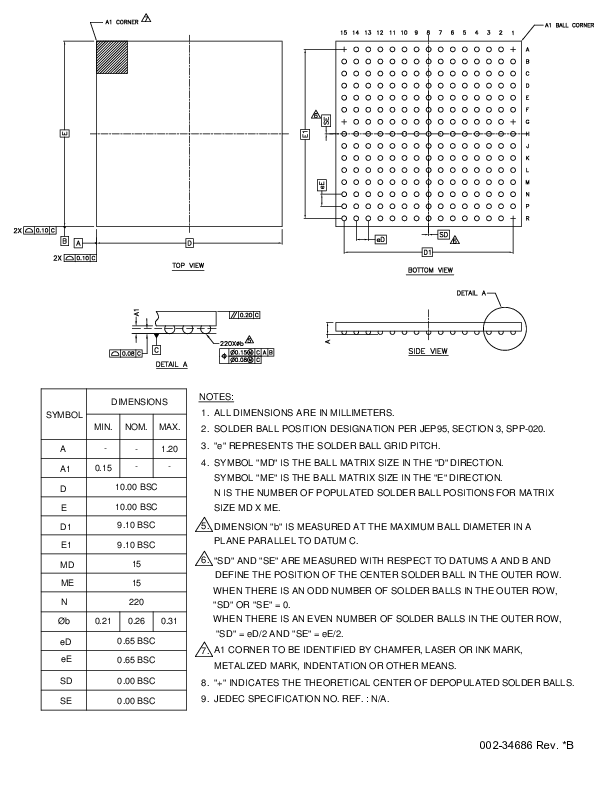
Figure 18.
eWLB-235, 7 x 7 x 0.7
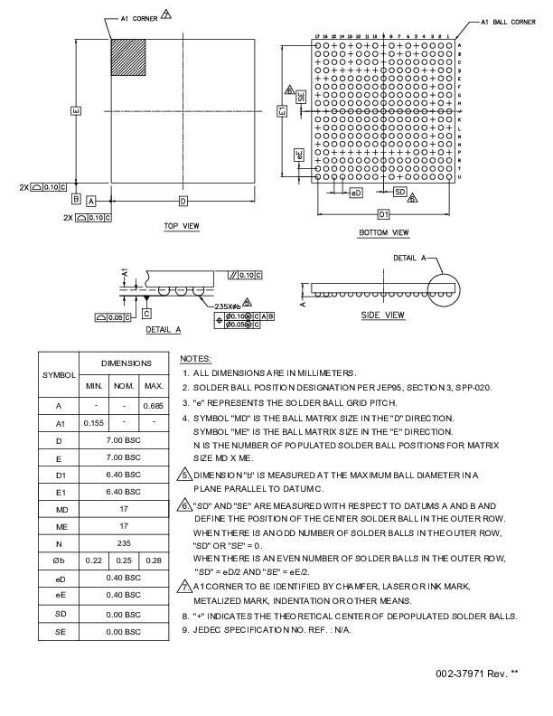
Figure 19.
WLB-154, 5.22 x 4.32 x 0.505
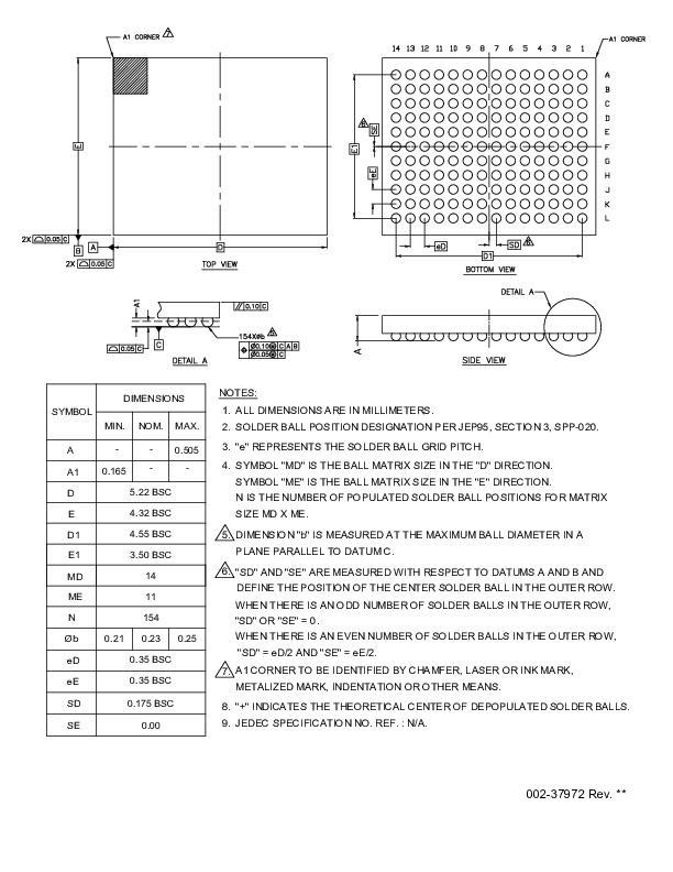
Errata
This section describes the errata for the PSOC™ Edge E8 product line. Details include errata trigger conditions, scope of impact, available workarounds, and silicon revision applicability.
For more details, contact
Infineon support
.
Part numbers affected
Part number | Device characteristics |
|---|---|
All | PSOC™ Edge E8 product line |
PSOC™ Edge E8 qualification status
Silicon in Process
PSOC™ Edge E8 errata summary
This table defines the errata applicability to available product line devices.
Note:
Errata items, in the table below, are hyperlinked. Click on any item entry to jump to its description.
Items | PSOC™ Edge E8 | Silicon revision | Fix status |
|---|---|---|---|
[1]. Autonomous analog wake up timer glitch | All | 1 (B0) | Fix planned for B1 silicon revision |
[2]. 3.3 V GPIO high leakage | All | 1 (B0) | Fix planned for B1 silicon revision |
| |
|---|---|
Problem definition | The 16-bit wake up timer of autonomous analog may produce terminal count (TC) events inconsistent with the count value written to the timer. This TC event is responsible for triggering the TIMER_DONE_WAKE condition used by the autonomous analog's state transition table for timing purposes. This condition is used for triggering and power-cycling the ADC and the other analog blocks at periodic intervals. |
Parameters affected | Inconsistent or missing terminal count from the wake up timer. |
Trigger condition(s) | Whenever the wake up timer is used (TIMER_DONE_WAKE condition in the state transition table). |
Scope of impact | Lack of timed power-cycling of the ADC and the analog blocks. This results in higher power consumption because duty cycling is not possible with the internal timer. |
Workaround | Do not use the autonomous analog's wake up timer and the TIMER_DONE_WAKE condition:
These workarounds will still be completely functional in B1 silicon revision. |
Fix status | Will be fixed in B1 silicon
revision. |
| |
|---|---|
Problem definition | 3.3 V capable GPIOs (ports P16 and P17) on some devices show higher leakage than expected in their 3.3 V range of operation. |
Parameters affected | No specific parameters beyond leakage are affected. 3.3 V capable ports are still fully functional and can be used normally at their 3.3 V range for evaluation and development and prototype builds. Note the same Ports can be used in 1.8 V mode powered by a 1.8 V supply with full 1.8 V spec compliance. |
Trigger condition(s) | Use of 3.3 V range of 3.3 V capable GPIOs |
Scope of impact | Inability to use 3.3 V range of 3.3 V capable GPIOs in production on B0 silicon with leakage spec compliance |
Workaround | Use 3.3 V GPIOs for evaluation and development and prototype builds |
Fix status | Will be fixed in B1 silicon |
Acronyms
Acronym | Description |
|---|---|
AAD | acoustic activity detection |
ADC | analog-to-digital converter |
AES | advanced encryption standard |
AVB | audio video bridging |
AXI | advanced extensible interface |
BLE | Bluetooth® low energy |
BOD | brown-out detect |
BT | Bluetooth® |
CAN | controller area network |
CANFD | controller area network flexible data-rate |
CMOS | complementary metal oxide semiconductor |
CPU | central processing unit |
CRC | cyclic redundancy checker |
CRYPTO | cryptographic accelerator |
DAC | digital to analog converter |
DBI | display bus interface |
D-Cache | data cache |
DES | data encryption standard |
DICE | device identifier composition engine |
DMA | direct memory access |
DPLL | digital phase locked loop |
DSI | digital Serial Interface (Usually in relation to MIPI DSI) |
DSP | digital signal processor |
D-TCM | data tightly coupled memory |
ECC | error correcting code |
ECC | elliptic curve cryptography |
ECO | external crystal oscillators |
EEPROM | electrically erasable programmable read-only memory |
eMMC | embedded multimedia card |
EPC | edge protect category |
ETM | embedded trace macrocell |
FIFO | first in, first out |
FPU | floating point unit |
GPIO | general purpose input/output |
GPU | graphics processing unit |
HDR | high data rate |
HFCLK DIV | high frequency clock divider |
HMI | human-machine interface |
HP | high performance |
HPDMA | high performance direct memory access |
HS USB | Hi-Speed universal serial bus |
HSIOM | high-speed I/O matrix |
HUK | hardware unique key |
I2C | inter-integrated circuit |
I2S | inter IC sound bus |
I3C | improved inter integrated circuit |
I-cache | instruction-cache |
IDAU | implementation defined attribution unit |
IHO | internal high-speed oscillator |
IMO | internal main oscillator |
IO | input output |
IPC | inter-processor communication |
IRQ | interrupt request |
ISR | interrupt service routine |
I-TCM | instruction tighlty coupled memory |
JTAG | joint test action group |
LDO | low dropout |
LP | low power |
LPComp | low-power comparator |
LUT | lookup table |
LVD | low-voltage detection |
LVTTL | low-voltage transistor-transistor logic |
MAC | media access control |
MEMS | micro electro mechanical systems |
MIPI | mobile industry prepocessor interface |
ML | machine learning |
MMIO | memory mapped I/O |
MPC | memory protection controller |
MPU | memory protection unit |
MTB | micro trace buffer |
MVE | m-profile vector extension |
NNLite | neural network lite |
NVIC | nested vectored interrupt controller |
NVM | non volatile memory |
OTF | on-the-fly |
OTP | one-time programmable |
OVD | over voltage detection |
OVT | over voltage tolerant |
PAL | programmable array logic |
PC | protection context |
PCM | pulse code modulation |
PDL | peripheral driver library |
PDM | pulse density modulation |
PGA | programmable gain amplifier |
PHY | physical layer |
PILO | precision Internal Low-speed Oscillator |
PLD | programmable logic device |
PLL | phase-locked loops |
PMU | power management unit |
POR | power-on reset |
PPC | peripheral protection controller |
PRNG | pseudo random number generator |
PSA | platform security architecture |
PTCOMP | programmable threshold comparator |
QoS | quality of service |
ROM | read-only memory |
RoT | root of trust |
RRAM | resistive random access memory |
RSA | rivest-shamir-adleman, a public-key cryptography algorithm |
RTC | real-time clock |
RTOS | real time operating system |
SAR | successive approximation register |
SAU | secure attribution unit |
SCA | side channel attack |
SCB | serial communication blocks |
SD | secure digital |
SDHC | secure digital host controller |
SDIO | secure digital input output |
SDK | software development kit |
SDR | single data rate |
SHA | secure hash algorithm |
SISO | single in single out |
SMIF | serial memory interface |
SNR | signal-to-noise ratio |
SoCMEM | system on chip memory, also called system SRAM |
SOD | speech onset detection |
SPI | serial peripheral interface |
SRAM | static random access memory |
SRES | software reset |
SRSS | system resources subsystem |
TCPWM | timer/counter pulse-width modulator |
TDM | time division multiplexing |
TIA | transimpedance amplifier |
TPIU | trace port interface unit |
TRNG | true random number generator |
UART | universal asynchronous transmitter receiver |
UDS | unique device secret |
ULP | ultra low power |
USB | universal serial bus |
VLAN | virtual local area network |
WCO | watch crystal oscillator |
WDT | watch dog timer |
WFE | wait for event |
WIC | wakeup interrupt controller |
Wifi | wireless fidelity |
XIP | execute-in-place |
XRES | external reset |
Document conventions
Units of measure
Symbol | Units of measure |
|---|---|
°C | Degree Celsius |
KB | 1024 bytes |
kHz | Kilohertz |
Mbps | Megabits per second |
Msps | Megasamples per second |
MHz | Megahertz |
ns | Nanosecond |
% | Percent |
V | Volt |
mV | Millivolt |
Ω | Ohm |
kΩ | Kiloohm |
MΩ | Megaohm |
µF | Microfarad |
µH | Microhenry |
µs | Microseconds |
ms | Millisecond |
ps | Picosecond |
MB | Megabyte |
ksps | Kilosamples per second |
pF | Picofarad |
F | Farad |
µA | Microampere |
mA | Milliampere |
nA | Nanoampere |
µW | Microwatt |
dB | Decibel |
FSR | Full scale range |
ppm | Parts per million |
Revision history
Document revision | Date | Description of changes |
|---|---|---|
*J | 2025-11-04 | Release to web |
Trademarks
The Bluetooth® word mark and logos are registered trademarks owned by Bluetooth SIG, Inc., and any use of such marks by Infineon is under license.
PSOC™, formerly known as PSoC™, is a trademark of Infineon Technologies. Any references to PSoC™ in this document or others shall be deemed to refer to PSOC™.
2
These pins are connected to GND for E81 and E83 series devices
3
These pins are NC for E81 and E83 series devices
4
This pin is input-only