PSOC™ Edge E8x2, E8x3, E8x5, E8x6 architecture reference manual
About this document
Scope and purpose
This document describes the Infineon PSOC™ Edge E8x2, E8x3, E8x5, E8x6 series of microcontroller. This is a 32-bit, dual-CPU, high-performance, and low-power MCU family designed for compute performance, human-machine interface (HMI), machine learning (ML), enhanced sensing, real-time control, and low-power applications.
Intended audience
This document is intended for embedded hardware engineers, software developers, and system architects who want to understand the architecture of the Infineon PSOC™ Edge E8x2, E8x3, E8x5, E8x6 series of microcontroller.
Introduction
Detailed features
This product line has the following features:
Always-on domain
Acoustic activity detection
ADC, opamps, comparator, and DACs
Autonomous Analog
2x Continuous-Time Blocks (CTB) offering Analog Front-End (AFE) functions such as:
Programmable Gain Amplifier (PGA)
Transimpedance Amplifier (TIA)
Pseudo-Differential Amplifier
Comparator
SAR ADC with
5 Msps sample rate at 12 bits or 250 ksps at 16 bits in System High Performance mode
200 ksps sample rate at 12 bits or 12.5 ksps at 16 bits in System Deep-Sleep mode
Accumulation and averaging – 2x, 4x, 8x … 256x
Limit detection, Offset and gain calibration
2x 12-bit DAC with 1 μS refresh time, automatic waveform generation
2x Programmable Threshold Comparators (PTComp) with post-processing supporting Audio Activity Detection (AAD) and Motor Control
Autonomous Controller capable of performing following functions in Device DeepSleep Mode
Power cycling of individual blocks
Send triggers and/or interrupts to the CPU
Digital output to as many as four GPIOs
Security features
Up to Infineon Edge Protect Category 4 (EPC 4), depending on the part numbers mentioned in the ordering information section of the corresponding PSOC™ Edge datasheets
Lockstep Secure Enclave in low-power always-on domain
Secure Infineon RoT key storage; secure boot
Tamper detection, side channel attack (SCA) mitigation, and protection against fault injection attacks
On EPC 4 part numbers only: Secure Enclave runtime services for Arm® Platform Security Architecture (PSA) compliant cryptography, key management, secure storage and attestation services
Off‑the‑shelf Trusted Firmware‑M enablement and Mbed‑TLS for crypto operations
Secure isolation of processing environments via Arm® TrustZone with root-of-trust established at boot by Cortex®‑M33 CPU
Factory provisioned device unique keypair (DICE_DeviceID), Hardware Unique Key (HUK), Unique Device Secret (UDS) and Infineon device certificates
Infineon proprietary protection units for memory and peripherals
Secure firmware update; secure debug, secure RMA mode for field failure analysis
Low‑power security, control, and communication CPU
Cortex®‑M33 with FPU, DSP, and MPU at 200 MHz in System High Performance (HP) power mode
16‑KB I‑cache
RRAM module for NVM
DMA
Hardware crypto accelerator with comprehensive support of cryptographic algorithms
High-performance compute, DSP, and machine learning (ML) blocks
Cortex®‑M55 CPU with DSP extension at 400 MHz in System High Performance (HP) power mode
FPU, MVE extension with vectored fixed and floating point
32‑KB I‑cache and 32‑KB D‑cache
256‑KB I- and 256‑KB D‑TCMs
Ethos-U55 NN coprocessor with 128 multiply-accumulate operations (MACs) per cycle; 51.2 billion operations per second
HPDMA
Multi‑AXI high‑bandwidth interconnect
Communications and connectivity
HS USB host/device, 480 Mbps
SD host controllers with eMMC mode
2x Serial memory interfaces (SMIF with 32 KB cache ) with octal DDR
Ethernet 10/100 media access control (MAC)
CAN FD
I3C bus for 2‑wire sensor hubs
I 2 C, SPI, and UART via serial communication blocks (SCB). SCB0 supports only I 2 C and SPI
HMI functional blocks
2.5D graphics processor for rendering images and text
Display controller with MIPI DSI
Audio: PDM microphone interface with 3 pairs of inputs, 2x TDM (Time Division Multiplexing) with 8 channels each interface, supporting I2S full and half-duplex modes
Optimizable power
Independent voltage domains allowing selectable domain power for low-power or high-performance
Active, sleep, deep sleep, and hibernate modes
On‑chip DC‑DC buck converter
Dynamic frequency scaling for real‑time power optimization
Granular SRAM blocks for selectable SRAM retention
Programmable GPIO pins
Programmable drive modes, strengths, and slew rates
Over‑voltage tolerant (OVT) pins for I 2 C compliance
RTC with 16 backup registers
ModusToolbox™ design environment
Code development and debugging in a cross-OS (Windows, Linux, Mac OS) IDE-neutral environment supporting Visual Studio Code, IAR, Keil and Eclipse IDEs
Installable software development kits (SDK) for peripheral initialization, clock and pin configuration, and middleware selection
Peripheral driver library (PDL) for peripheral APIs, including SD host controller for connection to IoT devices; and ML library
Industry-standard CMSIS pack support
RTOS support, including FreeRTOS
DEEPCRAFT™ Studio enabling the full journey from ML model development to embedded software
Architecture
Document organization and conventions
Major sections
The information in this reference manual is organized as follows:
section – Presents the chapters specific to an individual aspect of the device. These are the detailed implementation and use information for some aspect of the integrated circuit
Registers Reference Manual – Supplies all device register details summarized in the reference manual. This is an additional document
Documentation conventions
Register conventions
Register conventions are detailed in the Registers Reference Manual .
Numeric naming
Hexadecimal numbers are represented with all letters in uppercase with an appended lowercase ‘h’ (for example, ‘14h’ or 3Ah) and hexadecimal numbers may also be represented by a ‘0x’ prefix, the C coding convention. Binary numbers have an appended lowercase ‘b’ (for example, 01010100b or 01000011b’). Numbers not indicated by an ‘h’ or ‘b’ are decimal.
Units of measure
lists the units of measure used in this document.
Abbreviation | Unit of measure |
|---|---|
bps | bits per second |
°C | degrees Celsius |
dB | decibels |
dBm | decibels-milliwatts |
fF | femto Farads |
G | Giga |
Hz | Hertz |
k | kilo, 1000 |
K | kilo, 2 10 |
KB | 1024 bytes, or approximately 1000 bytes |
Kbit | 1024 bits |
kHz | kilohertz |
kΩ | kilo ohms |
MHz | mega hertz |
MΩ | mega ohms |
µA | micro amperes |
µF | micro Farads |
µs | micro seconds |
µV | micro volts |
µVrms | micro volts root-mean-squared |
mA | milli amperes |
ms | milli seconds |
mV | milli volts |
nA | nano amperes |
ns | nano seconds |
nV | nano volts |
Ω | Ohms |
pF | pico farads |
pp | peak-to-peak |
ppm | parts per million |
SPS | samples per second |
σ | sigma: one standard deviation |
V | Volts |
Acronyms and initializations
lists the acronyms and initializations used in this document.
Acronym | Definition |
|---|---|
ACG | Access Control Gating |
ADC | Analog-to-Digital Converters |
AES | Advanced Encryption Standard |
AHB | AMBA (advanced microcontroller bus architecture) high-performance bus, an Arm® data transfer bus |
AIRCR | Application Interrupt and Reset Control Register |
AIU | Application Interface Unit |
APBIC | Advanced Peripheral Bus Interconnect |
APPCPUSS | Application CPU Subsystem |
ASIC | Application Specific Integrated Circuit |
ATB | Advanced Trace Bus |
AUTOSAR | Automotive Open System Architecture |
AXI | Advanced Extensible Interface |
BLE | Bluetooth® Low Energy |
BNA | Buffer Not Available |
BOD | Brownout Detect |
BREG | Backup Register |
BRESP | AXI Write Transaction Response Signal |
BT | Bluetooth® |
C-AHB | Code AHB Interface |
CAN-FD | Controller Area Network Flexible Data-rate |
CBOR | Concise Binary Object Representation |
CCC | Common Command Code |
CDR | Clock Data Recovery |
CFI | Canonical Format Indicator |
CIC | Cascaded Integrator Comb |
CMD_RESP | Command Response |
CMOS | Complementary Metal-Oxide Semiconductor |
CoT | Chain of Trust |
CPHA | Clock Phase |
CPOL | Clock Polarity |
CPU | Central Processing Unit |
CQE | Command Queue Engine |
CRC | Cyclic Redundancy Checker |
CSV | Clock Supervision |
CTB | Continuous Time Block |
CTB | Continuous Time Block (Opamp Circuits) |
CTI | Cross Trigger Interface |
CTM | Cross Trigger Matrix |
D-Cache | Data Cache |
D-PHY | MIPI Physical layer standard used for MIPI DSI and CSI |
DAA | Dynamic Address Allocation |
DAP | Debug Access Port |
DAR | Disable automatic retransmission |
DBI | Display Bus Interface |
DBTP | Data Bit Timing and Prescaler Register |
DCR | Device Characteristics Register |
DDR | Double Data Rate |
DE | Data Enable |
DEMCR | Debug Exception and Monitor Control Register |
DES | Data Encryption Standard |
DHCSR | Debug Halting Control and Status Register |
DICE | Device Identifier Composition Engine |
DMA | Direct Memory Access |
DMAC | Direct Memory Access Controller |
DP | Debug Port |
DPI | Display Pixel Interface |
DPLL | Digital Phase Locked Loop |
DPU | Display Processor Unit |
DSI | Digital Serial Interface (Usually in relation to MIPI DSI) |
DSP | Digital Signal Processing |
DTCM | Data Tightly Coupled Memory |
DU | Data unit |
DW | Data Wire |
DWRR | Deficit Weighted Round Robin |
E2E | End-to-End |
ECC | Error Correcting Code |
ECO | External Crystal Oscillator |
ECT | Embedded Cross Triggering |
EDC | Error Detection and Correction |
EFEC | Extended Filter Elements Configuration |
Em_EEPROM | Emulated Electrically Erasable Programmable Read-only Memory |
EMAC | Ethernet Media Access Controller |
eMMC | Embedded Multimedia Card |
EOL | End of List |
EOPF | End-of-Periodic-Frame Boundary |
EP | Endpoint |
ESD | Electrostatic Discharge |
ETB | Embedded Trace Buffer |
ETF | Embedded Trace Fifo |
ETM | Embedded Trace Macrocell |
ETS | Enhanced Transmission Selection |
FCS | Frame Check Sequence |
FIFO | First In First Out |
FIH | Fault Injection Hardening |
FIR | Finite Impulse Response |
FPU | Floating Point Unit |
FS | Full Speed |
GFC | Global Filter Configuration |
GPIO | General Purpose Input Output |
GPU | Graphics Processing Unit |
HAR | Human Activity Recognition |
HCI | Host Controller Interface |
HDR | High Date Rate |
Hi-Z | High Impedance |
HPDMA | High Performance Direct Memory Access |
HSIOM | High Speed I/O Matrix |
HSM | Hardware Security Module |
HUK | Hardware Unique Key |
HV | High Voltage |
I2C | Inter-Integrated Circuit |
I2S | Inter-IC Sound Bus |
I3C | Improved Inter-Integrated Circuit |
I-Cache | Instruction Cache |
I/O | Input/Output |
IBI | In-band Interrupts |
ICER | Interrupt Clear Enable Register |
IDAU | Implementation Defined Attribution Unit |
IMO | Internal Main Oscillator |
IOC | Interrupt on Complete |
IP | Internet Protocol |
IPC | Inter Processor Communication |
IRQ | Interrupt Request |
ISB | Instruction Synchronization Barrier |
ISER | Interrupt Set Enable Register |
ISR | Interrupt Service Routine |
ITCM | Instructions Tightly Coupled Memory |
ITM | Instrumentation Trace Macrocell |
ITNS | Interrupt Target Non-secure |
JTAG | Joint Test Action Group |
LCD | Liquid Crystal Display |
LCS | Life Cycle State |
LIN | Local Interconnect Network |
LLDP | Link Layer Discovery Protocol |
LP | Low Power |
LPCOMP | Low-Power Comparator |
LPI | Low Power Idle |
LPM | Link Power Management |
LS | Low Speed |
LSB | Least significant Byte |
LUT | Look-up Table |
LVD | Low Voltage Detector |
LVTTL | Low Voltage Transistor-Transistor Logic |
M-AXI | Master AXI Interface |
MAC | Media Access Control |
MCU | Microcontroller Unit |
MCWDT | Multi-counter Watchdog Timer |
MDC | MDIO interface clock |
MDIO | Management Data Input/Output |
MII | Media-Independent Interface |
MIPI | Mobile Industry Processor Interface |
MISO | Master-in-slave-out |
ML | Machine Learning |
MMIO | Memory-mapped I/O |
MNR | Message Number |
MOSI | Master-out-slave-in |
MPC | Memory Protection Controller |
MPU | Memory Protection Unit |
MR | Master Request |
MRAM | Message RAM |
MRL | Maximum Read Length |
MSB | Most significant Byte |
MSC | Master Security Controller |
MSP | Main Stack Pointer |
MTQ | Minimum Time Quanta |
MVE | M-profile Vector Extension |
MWL | Maximum Write Length |
NBTP | Nominal Bit Timing and Prescaler Register |
NMI | Non-maskable Interrupt |
NN | Neural Network |
NPU | Neural Processing Unit |
NTU | Network Time Unit |
NVIC | Nested Vectored Interrupt Controller |
NVM | Non-Volatile Memory |
OEM | Original Equipment Manufacturer |
OPC | Opcode |
OTP | One-Time-Programmable Memory |
OVD | Over Voltage Detector |
OVP | Over Voltage Protection |
OVT | Over Voltage Tolerant |
P2P | Peer-to-Peer |
P-AHB | Peripheral AHB Interface |
PC | Protection Context |
PCM | Pulse Code Modulation |
PDM | Pulse Density Modulation |
PEC | Packet Error Check |
PendSV | Pending Supervisory |
PERI | Peripheral |
PHY | Ethernet Physical (transceiver component) |
PID | Product Identification |
PILO | Precision Internal Low-speed Oscillator |
PKC | Public-Key Cryptography |
PLL | Phase Locked Loop |
POR | Power-on Reset |
PPB | Private Peripheral Bus |
PPC | Peripheral Protection Controller |
PPU | Power Policy Unit |
PRB | Programmable Reference Block |
PRNG | Pseudo Random Number Generator |
PSA | Platform Security Architecture |
PSP | Process Stack Pointer |
PSR | Program and Status Register |
PSRR | Power Supply Rejection Ratio |
PTComp | Programmable Threshold Comparator |
PTM | Pulse Time Modulation |
PTP | Precision Time Protocol |
PWM | Pulse-Width Modulation |
RMII | Reduced Media-Independent Interface |
RoT | Root of Trust |
RRAM | Resistive Random Access Memory |
RRAMC | RRAM Controller |
RRESP | AXI Read Transaction Response Signal |
RTC | Real-Time Clock |
RTOS | Real-time Operating System |
RWDS | Read-Write-Data-Strobe |
RX | Receive |
RZWI | Read Zero Write Ignore |
S-AHB | Slave AHB Interface |
SAR | Successive-Approximation-Register |
SAU | Secure Attribution Unit |
SCB | Serial Communication Block |
SCL | Serial Clock |
SDA | Serial Data |
SDHC | Secure Digital Host Controller |
SDIO | Secure Digital Input Output |
SDR | Single Data Rate |
SESIP | Security Evaluation Standard for IoT Platforms |
SFD | Start Frame Delimiter |
SFEC | Standard Filter Element Configuration |
SFR | Special Function Register |
SHA | Secure Hash Algorithm |
SHCSR | System Handler Control and State Register |
SHPR | System Handler Priority Registers |
SIDFC | Standard ID Filter Configuration |
SIMD | Single Instruction/Multiple Data |
SIO | Special Input/Output |
SIR | Slave Interrupt Request |
SMI | Serial Management Interface |
SMIF | Serial Memory Interface |
SNAP | Subnetwork Access Protocol |
SoC | System on Chip |
SoCMEM | System On Chip Memory |
SOF | Start of Frame |
SPI | Serial Peripheral Interface |
SPRAM | Single Port RAM |
SRAM | Static Random Access Memory |
SRAMC | Static Random Access Memory Controller |
SROM | Supervisory Read Only Memory |
SRSS | System Resources Sub System |
STT | State-Transition Table |
SVCall | Supervisory Call |
SWD | Serial Wire Debug |
SWO | Serial Wire Output |
SWV | Serial Wire Viewer |
SYSCPUSS | System CPU Subsystem |
TAP | Test Access Port |
TCK | Test Clock |
TCP/IP | Transmission Control Protocol/Internet Protocol |
TCPWM | Timer/Counter Pulse-Width Modulator |
TDES | Triple Data Encryption Standard |
TDI | Test Data In |
TDM | Time-Division Multiplexing |
TDO | Test Data Out |
TM | Time Mark |
TMEX | Time Mark Event External |
TMIN | Time Mark Event Internal |
TMS | Test Mode Select |
TPA | Trace Port Analyzer |
TPIU | Trace Port Interface Unit |
TRN | Turnaround Period |
TRNG | True Random Number Generator |
TSU | Timestamp Unit |
TTCAN | Time-Triggered CAN |
TTL | Transistor-Transistor Logic |
TX | Transmit |
UART | Universal Asynchronous Receiver Transmitter |
UDP | User Datagram Protocol |
ULP | Ultra Low Power |
USB CTRL | USB Controller |
USB OTG | USB On-The-Go |
USB PHY | USB Physical Layer |
USBHSSS | Universal Serial Bus High Speed Subsystem |
UTMI | USB Transceiver Macrocell Interface |
VLAN | Virtual Local Area Network |
VREG | Voltage Regulator |
VTG | Video Timing Generation |
VTOR | Vector Table Offset Register |
VU | Vector Unit |
WDR | Watchdog Reset |
WDT | Watchdog Timer |
WFE | Wait For Event |
WFI | Wait For Interrupt |
WIC | Wakeup Interrupt Controller |
WWD | Wake Word Detection |
XIDAM | Extended ID AND Mask |
XIDFC | Extended ID Filter Configuration |
XIP | Execute-In-Place |
XN | Execute Never |
XRES | External Reset |
CPU subsystem (CPUSS)
The multi-core architecture of this product line includes the following central processing unit (CPU) and neural processing unit (NPU) subsystems:
Secure Enclave
System CPU subsystem (SYSCPUSS)
Application CPU subsystem (APPCPUSS)
NPU subsystem (NPUSS)
The Secure Enclave is implemented in the low-power, always-on domain using Arm® Cortex®-M0+ processors operating in lock-step mode. It provides a secure boot process that includes Root of Trust (RoT) and Device Identifier Composition Engine (DICE) mechanisms for device attestation. It is the first subsystem to boot up on every reset and executes the secure boot code. The Secure Enclave also manages the lifecycle state (LCS) and provides secure services to the SYSCPUSS.
Note:
The Secure Enclave is not programmable by the user.
The SYSCPUSS comprises a low-power, 32-bit Arm® Cortex®-M33 (CM33) CPU that manages security, control, and communication. The APPCPUSS is powered by an Arm® Cortex®-M55 (CM55) processor, which supports M-profile vector extension (MVE), also known as Arm® Helium technology. The APPCPUSS is responsible for compute, digital signal processing (DSP), and machine learning (ML) capabilities.
Additionally, the Arm® Ethos-U55-based NPUSS is integrated with the APPCPUSS to enhance the inferencing capabilities of neural networks (NNs), enabling applications such as automatic speech recognition and keyword detection.
This section provides an overview of the Arm® Cortex® CPUs and NPU in the
PSOC™ Edge E84
MCU family. For more details, see the Arm® documentation sets for
Cortex®-M33
,
Cortex®-M55
,
Cortex®-M0+
, and
Ethos-U55
.
Features
The PSOC™ Edge E84 MCU CPUs have the following features:
- Secure Enclave in the low-power, always-on domain :
Lock-step secured
2x CryptoLite blocks
- Cortex®-M33:
Maximum clock frequency of 200 MHz in System High-Performance (HP) mode
Single-precision floating-point unit (FPU), wake-up interrupt controller (WIC), and memory protection unit (MPU) with up to 8 regions per security state (secure and non-secure)
Integrated nested vectored interrupt controller (NVIC) supporting one non-maskable interrupt (NMI) and up to 480 physical interrupts with 8 to 256 priority levels
DSP extension
16 KB instruction cache (I-cache) on CM33 C-AHB bus with four-way set associativity
Supports TrustZone-M memory mapping for secure/non-secure aliasing based on a programmable secure attribution unit (SAU) and a fixed implementation-defined attribution unit (IDAU)
- Cortex®-M55 :
Maximum clock frequency of 400 MHz in System High-Performance (HP) mode
Supports scalar floating-point instructions for data formats of half-precision (16-bit, fp16), single-precision (32-bit, fp32), and double-precision (64-bit, fp64)
WIC and MPU with up to 12 regions for the non-secure state
Integrated NVIC supporting one NMI and up to 480 physical interrupts with 8 to 256 priority levels
Supports MVE and single instruction/multiple data (SIMD) 128-bit vector operations
32 KB each of I-cache and D-cache
256 KB each of instruction and data tightly coupled memories (ITCM and DTCM) without error-correcting code (ECC) support
NPUSS : Based on Arm® Ethos-U55, serving as a coprocessor with 128 multiply-accumulate operations (MACs) per cycle and 51.2 billion operations per second
- Additional features for both Cortex®-M33 and Cortex®-M55 CPUs :
Support for multiple Sleep modes with integrated wait-for-interrupt (WFI), wait-for-event (WFE), sleep-on-exit capability, and Sleep and Deep Sleep signals
Extensive debug support, including:
Serial wire debug (SWD) and Joint Test Action Group (JTAG) ports (SWJ)
Software and hardware breakpoints
Watchpoints
Trace support with 8-bit instrumentation trace macrocell (ITM) and embedded trace macrocell (ETM) interfaces, embedded trace buffer (ETB), and trace port interface unit (TPIU)
Cross-trigger interface (CTI)
Inter-processor communication (IPC) hardware - See
Inter processor communication (IPC)
Architecture
CM33 is a 32-bit processor with a 32-bit data path, 32-bit registers, and a 32-bit memory interface. CM55, on the other hand, features a 64-bit AXI bus interface with a 64-bit-wide data path. Both CPUs support a wide variety of instructions in the Thumb instruction set and operate in Thread and Handler modes (see
Operating modes and privilege levels
). Additionally, the CM33 supports secure and non-secure security states based on its security extension. In contrast, CM55 resets to a non-secure state, as the security extension is not enabled.
The instruction set for both the CM33 and CM55 CPU includes the following:
Signed and unsigned 32×32 -> 32-bit and 32×32 -> 64-bit multiply and multiply-accumulate operations, all executed in a single cycle
Signed and unsigned 32-bit division operations that require 2 to 11 cycles, depending on the values
DSP instructions
Complex memory load and store operations
Complex bit manipulations
The CM55 processor includes floating-point computation functionality provided by the MVE and FPU extensions. Similarly, the CM33 processor, when equipped with an FPU, supports single-precision arithmetic as defined by the FPv5 architecture. Both processors comply with ANSI/IEEE Std 754-2008, the IEEE standard for binary floating-point arithmetic.
Secure Enclave
The Secure Enclave consists of two Cortex®-M0+ processors based on the Armv6-M architecture running in lock-step mode. This Secure Enclave provides the initial Root of Trust (RoT), platform security architecture (PSA)-compliant cryptographic services, and lifecycle management for the device.
The Secure Enclave provides cryptographic services in a walled-off environment designed to achieve in-field security assurance at the Common Criteria AVA.VAN.4 level (25 JIL score).
The Secure Enclave is the first subsystem to boot after a reset and executes the secure boot code. This secure boot code acts as the RoT. Once the Secure Enclave is booted and secured, it extends the chain of trust to the CM33 in SYSCPUSS. For more information, see
Secure boot
.
Note:
SYSCPUSS communicates with the Secure Enclave exclusively through a dedicated IPC-channel interrupt. It has no direct control over the facilities within the Secure Enclave.
The main components of the Secure Enclave are:
Two Arm® Cortex®-M0+ processors running in lock-step
Two CryptoLite accelerators running in lock-step mode. For details on the components present, see
CryptoLite block
Dedicated ROM and SRAM for secure code execution, inaccessible from outside the Secure Enclave
The Secure Enclave supports the following AHB5 master interconnects:
32-bit system (SYS) AHB5 bus to SYSCPUSS
The Secure Enclave uses dedicated protection contexts to provide isolated execution, segregating sensitive operations from the rest of the system. Combined with the lock-step architecture, this creates a robust foundation for tamper resistance and ensures the secure execution of critical operations.
The Secure Enclave on the
PSOC™ Edge E84
device provides a secure storage mechanism utilizing the protected non-volatile memory (NVM) region to store user assets. This region is exclusively accessible by the Secure Enclave and is isolated from the rest of the system. Additionally, the Secure Enclave accesses RRAM through a dedicated protected port, providing secure and controlled access to sensitive data.
The Secure Enclave supports low-power modes for energy-saving options. Upon reset, the idle configuration for the Secure Enclave is set to Deep Sleep mode. The Secure Enclave transitions to Deep Sleep mode when idle and not servicing any requests. For additional power savings, the Secure Enclave can be shut off using runtime services. For more information on low-power modes, see
Device power modes
.
SYSCPUSS
The system CPU subsystem, also known as SYSCPUSS, is a low-power security, control, and communication CPU built on a Cortex®-M33 (CM33) core. It operates at frequencies of up to 200 MHz.
The CM33 CPU is a 3-stage pipeline (3PIP) processor from Arm®, based on the Armv8-M architecture. It operates within a low-power domain and supports rapid clock switching. The SYSCPUSS implements Arm® TrustZone-M-compatible security and protection infrastructure. It handles the initial boot process to establish security and protection schemes.
The CM33 CPU is a TrustZone-M processor with an inbuilt security extension. As part of this security extension, the CM33 includes a secure attribution unit (SAU) inside the CPU. The TrustZone-M architecture also defines an external interface for the CPU, which can be connected to an implementation-defined attribution unit (IDAU).
For non-CPU masters in SYSCPUSS, a master security controller (MSC) is instantiated along with the implementation-defined attribution unit (IDAU) to distinguish between secure and non-secure transfers. For more details, see
TrustZone
.
The SYSCPUSS includes a 16 KB, 4-way set-associative instruction cache (I-cache) on the C-AHB bus. The I-cache features a 128-bit prefetch buffer for quick refills in the event of a cache miss. SYSCPUSS supports an on-chip SRAM controller and associated memories, enabling C-AHB bus access from SRAM for code execution.
The SYSCPUSS features a 128-bit AHB5 bus interface for instruction fetch and data access from RRAM (NVM), internal SRAMs, system SRAM (also known as SoCMEM), and external memory connected via the SMIF interface. These are accessible through their aliased addresses. Additionally, SYSCPUSS provides a 32-bit AHB5 bus interface to access memory-mapped RRAM, internal SRAMs, system SRAM, peripherals, and external memory connected via SMIF, as defined in the system memory map (
Table 4
).
The SYSCPUSS includes two DMA controllers, each supporting 16 channels with Arm® Q-channel support. These channels are primarily used for servicing SCB and TCPWM peripherals.
The SYSCPUSS has one functional clock domain for the majority of hardware modules, two clock domains for debugging and testing, and optional clock domains for the SysTick timer of secure and non-secure systems.
Clock details:
clk_hf0 : Operates at up to 200 MHz in System High-Performance (HP) mode. This clock is used by the majority of SYSCPUSS components, including the instruction cache (I-cache), AHB bus infrastructure, DMA, MSC/IDAU/MPC, and all on-chip memory controllers. All components run at a single synchronous frequency with this clock
The following clocks are derived from clk_hf0 when the system is in Deep Sleep or Off modes:
clk_hf_cm33_act : Used by components that do not require a clock when the CM33 is in Sleep mode
clk_hf_cm33_sleep : Connected to the CM33 CLKPIN. This clock is gated in Deep Sleep power mode and free-running in all other power modes
clk_hf_dbg : Used for debug components. This clock is synchronous to clk_hf0 and is gated by the
swj_debug_ensignal
- Clock for secure and non-secure SysTick timers :Software can configure the SysTick timer to use clk_hf0 or an alternative clock source. A variety of clock sources provided by the SRSS can be selected for SysTick using the
CPUSS_SYSTICK_S_CTLandCPUSS_SYSTICK_NS_CTLMMIO registers.
The SYSCPUSS implements a centralized fault reporting infrastructure that requires only a single fault interrupt handler. This infrastructure captures faults related to various events, including (but not limited to) MPC or PPC violations, peripheral-specific errors, memory controller-specific errors such as ECC errors, processor cache or TCM ECC errors, and timeout errors.
The SYSCPUSS does not include a dedicated debug infrastructure. Instead, it shares a unified debug infrastructure with the APPCPUSS, which integrates Arm® CoreSight SoC-600 components. These components include the SWJ-DP DAP port, CTM, CTI, ATB bus, Funnel, ETB/ETF, TPIU-SoC-600, and ROM table. For more details, see
Program and debug interface
.
The SYSCPUSS incorporates a virtual-always-on low-power domain, which becomes active or initializes first by default after a power-on reset (POR). The SYSCPUSS power mode corresponds to the system power mode. The SRAM resides in the low-power domain, while the system SRAM, APPCPUSS, and NPUSS are in the high-performance domain. By default, the high-performance domain remains OFF (not powered) after POR and is only powered on when required by the CM33 software.
The SYSCPUSS includes the following power domains:
Active power domain
: This domain encompasses the majority of SYSCPUSS components, including the CM33 core logic, instruction caches (I-caches), AHB5 bus connection infrastructure and associated modules, all RRAM/SRAM memory controllers, and their attached memory protection contexts (MPCs) and exclusive access managers (EAMs) connected to the appropriate AHB bus
Deep Sleep power domain
: This domain includes the SYSCPUSS SWJ-DP debug interface and the wakeup interrupt controller (WIC) Deep Sleep wakeup logic. It supports wake-up functionality when SYSCPUSS is in Deep Sleep power mode
SRAM switched power domain
: Each SRAM module (DMA channel SRAM, cache data SRAM, MPC SRAM, and system SRAM) has a power switch allowing on/off or retention control during different system power modes
For more detailed information, see
Device power modes
.
APPCPUSS
The application CPU subsystem, also referred to as APPCPUSS, consists of a Cortex®-M55 (CM55) processor based on the Armv8.1-M mainline architecture. It operates at frequencies of up to 400 MHz and supports the MVE (Helium) extension. The APPCPUSS is designed to handle compute, DSP, and machine learning (ML) capabilities.
The APPCPUSS features 32 KB, 4-way set-associative instruction and data caches. Additionally, it includes 256 KB of ITCM (Instruction Tightly Coupled Memory) and 256 KB of DTCM (Data Tightly Coupled Memory).
The APPCPUSS implements three 64-bit AXI4 interfaces to connect to the system SRAM. It uses AHB5-to-AHB5 asynchronous bridges to communicate with the SYSCPUSS AHB5 infrastructure. Furthermore, it provides up to four extension slave ports for AXI5/AXI4 native devices, such as off-chip external memory connected via the SMIF interface. It includes a single high-performance DMA (HPDMA) controller with four engines. Each engine controls one DMA channel, and the engines arbitrate for bus master access.
The APPCPUSS has one functional clock domain for the majority of hardware modules, two clock domains for debugging and testing, and optional clock domains for the SysTick timer of secure and non-secure systems. The APPCPUSS operates asynchronously with SYSCPUSS.
Clock details:
clk_hf1
: Operates at up to 400 MHz in system high-performance (HP) mode. This clock is used by most APPCPUSS components, including the caches, AXI/AHB bus infrastructures, DMA, and system SRAM APPCPUSS ports. All components run at a single synchronous frequency, although the system SRAM can operate at a different frequency than clk_hf1
Clock for secure and non-secure SysTick timers
: Software can configure the SysTick timer to use
clk_hf1
or an alternative clock source. Various clock sources provided by the SRSS can be selected for SysTick using the
CPUSS_SYSTICK_S_CTL
and
CPUSS_SYSTICK_NS_CTL
MMIO registers
The APPCPUSS does not include a dedicated fault reporting infrastructure. Instead, all fault and interrupt events are routed to the fault reporting infrastructure within the SYSCPUSS.
The APPCPUSS includes the following power domains:
System Active power domain
: Includes the asynchronous AHB5 bridges within the APPCPUSS that interact with the SYSCPUSS. This domain is also referred to as the system low-power domain at the chip level
Application Active power domain
: Comprises the majority of the APPCPUSS logic, such as AXI/AHB infrastructures and the high-performance DMA controller (HPDMAC), excluding the CM55 CPU. This domain is also referred to as the application high-performance domain at the chip level
CM55 CPU power domain
: A dedicated power domain for the CM55 CPU, which exists as a sub-domain of the application active power domain
Deep Sleep power domain
: Includes power infrastructure components such as power policy units (PPUs), P/Q channel components, and the wakeup interrupt controller (WIC), supporting Deep Sleep power mode
For more detailed information, see
Device power modes
.
NPUSS
The NPU subsystem (NPUSS) includes the Arm® Ethos-U55 microNPU, which functions as a coprocessor for the APPCPUSS and operates in non-secure mode. It accelerates machine learning inference applications, such as automatic speech recognition and keyword identification.
The NPUSS is designed to target 8-bit and 16-bit integer-quantized neural networks (NNs). The Arm® Ethos-U55 microNPU supports multiply-and-accumulate (MAC) operations per cycle ranging from 32 to 256. In this NPUSS, the configuration is set to enable 128 MAC/cycle for the
PSOC™ Edge E84
MCU family.
The NPUSS supports active clock frequencies of up to 400 MHz, aligned with the APPCPUSS. As shown in
Figure 2
, the NPUSS is connected to the APPCPUSS through a 64-bit AXI interface. This interface is particularly critical for exchanging layer-specific inference data between the two subsystems.
The SRSS provides the clock to the NPUSS via the APPCPUSS peripheral interface. This same interface also supports register access through a 32-bit AHB5 interconnect, as shown in
Figure 2
.
Access to the NPUSS from the SYSCPUSS is possible through asynchronous bridges that connect the AHB interconnect in the SYSCPUSS domain to its counterpart in the APPCPUSS domain.
Figure 2.
NPUSS system diagram
The NPUSS consists of the following interfaces as shown in
Figure 3
:
AHB5 32-bit slave interface with wake-up signaling : Enables the device driver running on the CM55 APP CPU to access the control registers of the NPUSS
Two AMBA 5 AXI master interfaces : These interfaces are used by the integrated DMA controller of the NPUSS to access command streams:
M0 : A read/write capable master used for reading sample data and writing intermediate results to and from RAM
M1 : A read-only interface that provides parallel access to weights and layer-specific topology information from non-volatile memory. Although the NPUSS can access any memory within or outside the platform, the designated memory for its efficient operation is the system SRAM. Currently, the AXI0 and AXI1 ports in the system SRAM are dedicated to NPUSS access. SRAM can also be accessed via various AHB bridges in the platform
Two interrupt interfaces :
interrupt_npu : Used to asynchronously signal the completion of an operation (for example, inference cycle) or any errors
interrupt_ppu
: Used to communicate state transitions of the internal power policy unit (PPU) to the SRSS
Two Q-channel interfaces
: One Q-channel for the clock and one for power. These interfaces enable the system to automatically disable the NPU clock or power. The clock is otherwise free-running. The NPU does not quiesce while executing a task and typically does not quiesce if there are tasks in the job queue
Note:
Only the Power Q-Channel is utilized in the
PSOC™ Edge E84
MCU family; Clock Q-Channel is unused
Two clock domains
: Both clock domains are asynchronous to each other and reside in their own clock groups:
clk_hf
: High-frequency clock for the U55, AHB, and AXI interfaces
clk_pwr
: Clock for the Deep Sleep domain (PPU)
One reset signal
The Arm® Ethos-U55 consists of the following six components as shown in
Figure 3
:
Central control (CC)
: Manages the processing of neural networks, maintains synchronization, and handles data dependencies within the NPU
DMA controller
: Manages all transactions that use the Arm® AMBA 5 AXI interfaces
Clock and power module (CPM)
: Handles hard and soft resets and provides registers for current security settings, the main clock gate, and the Q-channel low-power interface (QLPI)
Weight decoder (WD)
: Reads the weight stream from the DMA controller. The decoder decompresses the stream and stores it in a double-buffered register, ready for consumption by the MAC unit
MAC unit
: Performs multiply-accumulate (MAC) operations required for convolution, depth-wise pooling, vector products, and the maximum operation used in maximum pooling
Output unit
: Reads finished accumulators from shared RAM and converts them into output activations. This process includes scaling each output feature map (OFM), adding bias values, and applying activation functions to individual points
Figure 3.
NPUSS block diagram
For more details, see the
Arm® Ethos-U55 NPU reference manual
.
The operating modes of the NPU are divided into three stages: pre-inference (referred to as configuration), inference, and post-inference. The APPCPUSS programs the memory location of the command stream and other payloads into the NPU registers via the AHB interface.
The command stream is generated by the Vela compiler, which takes a TFLite model as input and converts it into a TFLite model containing an Ethos-U operator for supported layers that can run on the NPU. This converted model is also referred to as the command stream. The Vela compiler is aware of the operators supported by the NPU. Further additional documentation, see
Vela compiler
.
Inference begins via the central control (CC) after the configuration phase is complete. Once started, the CC autonomously processes the command stream.
The power domain of the NPU operates on an 'on-demand' basis and is controlled by its own power policy unit (PPU). This power domain is directly dependent on the power domain of the APPCPUSS, meaning the APPCPUSS must be powered before the NPU.
The NPU PPU supports the following power modes:
ON
: Logic and RAM are powered ON and fully functional
OFF
: Logic and RAM are powered OFF, and all states are lost
ML capability (using NPUSS and APPCPUSS)
The CM55 processor in the APPCPUSS is the most AI-capable Cortex®-M processor of Arm® and the first to incorporate Arm® Helium technology. While the CM55 is fast enough to execute machine learning (ML) models designed for resource-constrained microcontrollers, its integration with the Arm® Ethos-U55-based NPUSS can accelerate ML inference in embedded systems by up to 480x.
The NPUSS is connected to the APPCPUSS via a 64-bit AXI interface, which facilitates the exchange of layer-specific inference data between the two subsystems.
To achieve optimized efficiency, the neural network (NN) model is trained offline and quantized. During quantization, weights are reduced to 8-bit values, and activations are reduced to either 8-bit or 16-bit values. Using the Vela compiler, the quantized model operators are converted into a command stream if the operators are supported by the NPU. The compiler determines which parts of a model operator can be optimized and executed on the NPU.
The NPU drivers manage workloads for inference execution on the NPU. When command stream operators are executed exclusively on the NPU, the external host application processor consumes negligible power. However, if some operators must run on the APPCPUSS, additional power is required. A TensorFlow Lite for microcontrollers (TFLμ)-based application running on the APPCPUSS calls the NPU driver. The driver configures the NPUSS registers and points to the starting address of the command stream, which includes weights, bias information, scale information, input feature maps (IFMs), output feature maps (OFMs), and input data.
The NPUSS uses its integrated DMA controller to fetch the command stream and autonomously performs inference. After executing the command stream, the NPUSS writes the results to shared RAM and asserts a maskable interrupt to notify the APPCPUSS. The driver handles this interrupt and passes the results to the next layers running on the APPCPUSS.
The software stack manages both control and data flows between the application software running on the APPCPUSS and the individual sub-components of the NPUSS. For more details, see the
Arm® Ethos-U55 NPU reference manual
.
Figure 4.
APPCPUSS - NPUSS control and data flow
Address and memory maps
All CPUs have a fixed address map with shared access to memory and peripherals, except for the Private Peripheral Bus (PPB) area. The PPB is a private address space dedicated to each core. The default memory map for all CPUs spans the range from
0x00000000
to
0xFFFFFFFF
, as shown in
Table 3
. This 32-bit (4 GB) address space is further partitioned into non-secure and secure memory regions, as shown in
Table 4
.
Based on Arm® TrustZone, bit [28] of the address indicates whether the memory is secure or Non-secure, resulting in the following memory map.
Address range (inclusive) | Region | Interface |
|---|---|---|
0x0000 0000 - 0x1FFF FFFF | Code | This region is primarily used to store program code but can also hold data. It includes the exception vector table, which starts at address .
|
0x2000 0000 - 0x3FFF FFFF | SRAM | Data region.
|
0x4000 0000 - 0x5FFF FFFF | Peripheral | This region contains all peripheral registers. Any attempt to execute instructions from this region results in a MemManage fault.
|
0x6000 0000 - 0x9FFF FFFF | External RAM | This region supports eXecute-in-place (XIP) functionality for external memory.
|
0xA000 0000 - 0xDFFF FFFF | External device | Not used in the PSOC™ Edge E84 MCU family. |
0xE000 0000 - 0xE00F FFFF | PPB | This region provides access to peripheral registers within the CPU core, including CPU and debug registers. |
0xE010 0000 - 0xFFFF FFFF | Vendor_SYS | Not used in the PSOC™ Edge E84 MCU family. |
Note:
Code can be executed from the Code, SRAM, and External RAM regions.
Access type | Address range | Subregion name | Size | Region name and interfaces |
|---|---|---|---|---|
Non-secure | 0x0000 0000 - 0x0003 FFFF | CM55 ITCM | 256 KB | Code region The internal instruction tightly coupled memory (ITCM) is used by the CM55 CPU (APPCPUSS) for code execution. |
Secure | 0x1000 0000 - 0x1003 FFFF | 256 KB | ||
Non-secure | 0x0080 0000 - 0x00FF FFFF | Reserved | 8 MB | Code region |
Secure | 0x1080 0000 - 0x10FF FFFF | 8 MB | ||
Non-secure | 0x0100 0000 - 0x01FF FFFF | Reserved | 16 MB | |
Secure | 0x1100 0000 - 0x11FF FFFF | 16 MB | ||
Non-secure | 0x0200 0000 - 0x0207 FFFF | RRAM (NVM - RRAM regions ) | 512 KB | Code region. Read-only memory is accessed through the C-AHB bus, as the I-cache operates in read-only mode. |
Secure | 0x1200 0000 - 0x1207 FFFF | 512 KB | ||
Non-secure | 0x0400 0000 - 0x040F FFFF | SRAM aliasing on CM33 C-AHB bus | 1 MB | Code region. The aliasing provides allocation for CM33 I-Cache to read from SRAM, system SRAM, or SMIF memories, which are originally allocated in the S-bus address space. |
Secure | 0x1400 0000 - 0x140F FFFF | 1 MB | ||
Non-secure | 0x0600 0000 - 0x064F FFFF | System SRAM (SoCMEM) aliasing on CM33 C-AHB bus | 5120 KB | |
Secure | 0x1600 0000 - 0x164F FFFF | 5120 KB | ||
Non-secure | 0x0800 0000 - 0x0BFF FFFF | SMIF0 (XIP PORT0) aliasing on C-AHB bus | 64 MB | |
Secure | 0x1800 0000 - 0x1BFF FFFF | 64 MB | ||
Non-secure | 0x0C00 0000 - 0x0FFF FFFF | SMIF1 (XIP PORT1) aliasing on C-AHB bus | 64 MB | |
Secure | 0x1C00 0000 - 0x1FFF FFFF | 64 MB | ||
Non-secure | 0x2000 0000 - 0x2003 FFFF | CM55 DTCM | 256 KB | SRAM region. Internal data tightly-coupled memory is used by the CM55 CPU (APPCPUSS) for low-latency data accesses. |
Secure | 0x3000 0000 - 0x3003 FFFF | 256 KB | ||
Non-secure | 0x2100 0000 - 0x21FF FFFF | Reserved | 16 MB | SRAM region. |
Secure | 0x3100 0000 - 0x31FF FFFF | 16 MB | ||
Non-secure | 0x2200 0000 - 0x2207 FFFF | RRAM (NVM) aliasing on S-AHB bus (for write) | 512 KB | SRAM region. The CM33 (SYSCPUSS) S-AHB bus uses the aliased address map to write into RRAM, which is originally allocated in the C-AHB bus address space. Reading from this address is functional but not preferred, as it is not cached by the CM33 I-cache. |
Secure | 0x3200 0000 - 0x3207 FFFF | 512 KB | ||
Non-secure | 0x2400 0000 - 0x240F FFFF | SRAM | 1 MB | SRAM region. |
Secure | 0x3400 0000 - 0x340F FFFF | 1 MB | ||
Non-secure | 0x2600 0000 - 0x264F FFFF | System SRAM (SoCMEM) | 5120 KB | |
Secure | 0x3600 0000 - 0x364F FFFF | 5120 KB | ||
Non-secure | 0x2800 0000 - 0x2FFF FFFF | Reserved | 128 MB | |
Secure | 0x3800 0000 - 0x3FFF FFFF | 128 MB | ||
Non-secure | 0x4000 0000 - 0x41FF FFFF | Secure Enclave Peripheral | 32 MB | Peripheral region.
|
Secure | 0x5000 0000 - 0x51FF FFFF | 32 MB | ||
Non-secure | 0x4200 0000 - 0x43FF FFFF | SYSCPUSS Peripheral (SYS MMIO) | 32 MB | |
Secure | 0x5200 0000 - 0x53FF FFFF | 32 MB | ||
Non-secure | 0x4400 0000 - 0x47FF FFFF | APPCPUSS Peripheral (APP MMIO) | 64 MB | |
Secure | 0x5400 0000 - 0x57FF FFFF | 64 MB | ||
Non-secure | 0x4800 0000 - 0x4803 FFFF | CM55 ITCM Peripheral | 256 KB | Peripheral region. The CM55 (APPCPUSS) internal TGU (TCM gating unit) implements security gating for TCM aliasing accesses. Additionally, TCM aliasing is further protected by the PPC. |
Secure | 0x5800 0000 - 0x5803 FFFF | 256 KB | ||
Non-secure | 0x4804 0000 - 0x4807 FFFF | CM55 DTCM Peripheral | 256 KB | |
Secure | 0x5804 0000 - 0x5807 FFFF | 256 KB | ||
Non-secure | 0x4C00 0000 - 0x4FFF FFFF | Reserved | 64 MB | Peripheral region. |
Secure | 0x5C00 0000 - 0x5FFF FFFF | 64 MB | ||
Non-secure | 0x6000 0000 - 0x63FF FFFF | SMIF0 | 64 MB | External RAM (external memory) region. External memories such as NOR flash or PSRAM can be mapped to this address space. This space is also aliased in the C-AHB bus space for reading through the I-cache. |
Secure | 0x7000 0000 - 0x73FF FFFF | 64 MB | ||
Non-secure | 0x6400 0000 - 0x67FF FFFF | SMIF1 | 64 MB | |
Secure | 0x7400 0000 - 0x77FF FFFF | 64 MB | ||
Non-secure | 0x6800 0000 - 0x6FFF FFFF | Reserved | 128 MB | |
Secure | 0x7800 0000 - 0x7FFF FFFF | 128 MB | ||
Non-secure | 0x8000 0000 - 0x8FFF FFFF | Reserved | 256 MB | |
Secure | 0x9000 0000 - 0x9FFF FFFF | 256 MB | ||
Non-secure | 0xA000 0000 - 0xAFFF FFFF | Reserved | 256 MB | External device region. |
Secure | 0xB000 0000 - 0xBFFF FFFF | 256 MB | ||
Non-secure | 0xC000 0000 - 0xCFFF FFFF | Reserved | 256 MB | |
Secure | 0xD000 0000 - 0xDFFF FFFF | 256 MB | ||
Non-secure | 0xE000 0000 - 0xE00F FFFF | PPB/EPPB | 1 MB | PPB region. Reserved for system control and debug. This region cannot be used for exception vector tables.
Any attempt to execute instructions from this region results in a MemManage fault. |
Secure | 0xF000 0000 - 0xF00F FFFF | 1 MB | ||
- | 0xE010 0000 - 0xFFFF FFFF | Reserved | 511 MB | Vendor_SYS region. |
Note:
Secure and non-secure memory pairs refer to the same physical memory, but they are mapped differently based on whether they are configured as secure or non-secure.
Gaps in the address space are reserved
Do not access these gaps; accessing them may result in hard faults or bus errors, depending on the bus segment or peripheral to which an address is allocated
The system uses a unified memory address space. Except for the CM55 ITCM/DTCM, almost all masters (CPUs, AXI/AHB DMA) access all memory structures and peripherals at the same memory locations. Coherency of caches and I/D TCMs for each CPU, as well as during protection context (PC) switches, is maintained by software.
For CM33, all accessible address space in RRAM is cacheable. Except for aliasing on SRAM, System SRAM, and external flash regions, no other area is cached.
For CM55, through its M-AXI bus, all flash, RRAM, System SRAM, and other accessible address space are cacheable in I/D caches, subject to the CPU MPU or Secure MPU control. The private I/D TCM memory space of the CPU is non-cacheable and not shareable with other CPUs.
All peripheral address space specified at 0x40000000 and 0x50000000 is not cacheable. XIP execution instructions from this address space cause a MemFault.
Address aliasing applies only to SRAM, System SRAM, and external flash when accessed by the CM33 processor via the code bus to facilitate code execution from these memories. Otherwise, these devices, along with all other addressable devices, are accessed by the CM55 processor through their globally defined memory addresses.
Note:
The
CM33_S_VECTOR_TABLE_BASE
,
CM33_NS_VECTOR_TABLE_BASE
,
CM55_S_VECTOR_TABLE_BASE
, and
CM55_NS_VECTOR_TABLE_BASE
registers determine the location of the secure and non-secure vector tables for the CM33 and CM55 CPUs, respectively.
Wait states and latencies
When accessing a memory area from the CPU, specifically the CM33 or CM55 cores, the primary focus is on the time required to retrieve data (read) at the relevant system operating frequencies. While write access times are also relevant, writes are typically posted, allowing the operation to proceed without immediate acknowledgment. In contrast, reads must traverse the full outbound address and control signal path, as well as the inbound data access path, which directly impacts system performance and response times.
This analysis is limited to scenarios where the CPU acts as the bus master. Other potential bus masters in the system are not considered in this context.
Generally, memory access time consists of two main components:
Wait states of the memories being read
Delay through the network interconnect (NIC)
Wait states (WS)
: This section focuses on wait states for RRAM and SRAM, which are of primary interest to users.
RRAM :
RRAM writes are significantly slower than RRAM reads (as is typical for most non-volatile memory) and are not considered in this context
RRAM reads are controlled by an internal 160 MHz read state machine clock, designed to produce data within 30 ns (also referred to as the "analog read time") regardless of the voltage mode (0.7 to 0.9 V)
In addition to the 30 ns analog read time, the following times are required for an RRAM read:
1 clock cycle for address read
1 clock cycle for ECC correction (assuming 0 or 1-bit correction; longer times are required for greater corrections)
Wait state calculation :
Based on the 30 ns read time, the WS value for a cycle time (Tcyc) in nanoseconds is calculated as
ceil(30/Tcyc)
Examples:
For an AHB clock frequency of 200 MHz (Tcyc = 5 ns), the WS value is 6
For an AHB clock frequency of 50 MHz (Tcyc = 20 ns), the WS value is 2
Voltage (V)
Frequency (MHz)
Wait states (WS)
0.9 (HP mode)
200
6
0.8 (LP mode)
80
3
0.7 (ULP mode)
50
2
SRAM :
All SRAMs are designed to operate with zero wait states at their peak target frequencies
This means that the address is latched on one clock edge, and the data is available on the next clock edge
Access cycles remain unaffected by voltage and frequency scaling. As long as the voltage and frequency limits are observed, all SRAM wait states remain at zero
Consequently, the number of cycles required to access SRAM (via
CLK_HF0
) and System SRAM (via
CLK_HF2
) does not change under normal operating conditions
Delay through the Network Inter-Connect (NIC)
:
Table 5.
CM33 CPU
Memory resource
Outbound clock cycles
Access time
Inbound clock cycles
Comment
RRAM
3 AHB clocks
Ceil(30 ns/AHB Tcyc)
2 AHB clocks
128-bit C-AHB. I-cache refill. 32-bit access is similar
SRAM
-
-
1 AHB clock
No wait states
System SRAM
3 AHB clocks
6 system SRAM clocks
2 AHB clocks
32-bit access and 128-bit access (parallel bank read)
Table 6.
CM55 CPU
Memory resource
Outbound clock cycles
Access time
Inbound clock cycles
Comment
RRAM
3 AXI + 5 AHB cycles
2 * Ceil(30 ns/AHB Tcyc)
4 AHB + 4 AXI cycles
64-bit word read takes 2 cycles
SRAM
3 AXI clocks + 3 AHB clocks
4 AHB cycles (2 accesses)
7 AXI clocks + 3 AHB clocks
64-bit word read takes 2 cycles
System SRAM
3 AXI clocks
6 system SRAM clocks
2 AXI clocks
The first word access takes one clock cycle, and each subsequent access requires one system SRAM clock cycle
Operating modes and privilege levels
The CM33 CPU supports both secure and non-secure states, while the CM55 operates only in the non-secure state. Both CPUs feature Thread and Handler operating modes and can operate in either the Thumb or Debug execution states.
Additionally, the processor can restrict or exclude access to certain resources by executing code in either privileged or unprivileged mode.
For more details on the modes of operation and execution, see
Armv8-M Architecture Reference Manual
.
Security states
When the Armv8-M security extension is included in the processor, the programmer's model incorporates two orthogonal security states: secure and non-secure. Since only the CM33 CPU has the security extension enabled, it always resets into the secure state.
Registers in the system control space are banked across the secure and non-secure states. The non-secure register view is accessible at an aliased address to the secure state.
Operating modes
For each security state, the processor can operate in Thread mode or Handler mode:
Thread mode
: Used to execute application software. The processor enters Thread mode on reset, or as a result of an exception return to Thread mode. Thread mode includes both privileged and unprivileged execution levels
Handler mode
: Used to handle exceptions. The processor enters Handler mode as a result of an exception. Handler mode operates only in the privileged execution level
The processor can switch security states when handling exceptions. For example, when a secure exception is triggered from the non-secure state, Thread mode transitions to Handler mode in the secure state.
Additionally, the processor can execute secure functions from the non-secure state or non-secure functions from the secure state. The Armv8-M Security Extension enforces requirements for such calls to ensure secure data cannot be accessed from the non-secure state.
Operating states
The processor can operate in either the Thumb state or the Debug state:
Thumb state
: Represents the normal execution state. Executes 16-bit and 32-bit halfword-aligned Thumb instructions
Debug state
: Represents the state when the processor is in halting debug mode
Privilege levels
Unprivileged
: The software has limited access to the
Move from General-purpose Register to Special Register (MSR)
and
Move from Special Register to General-purpose Register (MRS)
instructions. It cannot use the
Change Processor State/Disable Interrupts (CPSID)
or
Change Processor State/Enable Interrupts (CPSIE)
instructions. Additionally, it cannot access the system timer, NVIC, or system control block and has restricted access to memory and peripherals
Privileged
: Software has access to all resources and can execute all instructions
Thread mode
The
CONTROL
register determines whether software execution is privileged or unprivileged
Privileged software can write to the
CONTROL
register to change the privilege level
Unprivileged software can use the
SVC
instruction to transfer control to privileged software
Handler mode
Software execution is always privileged
The main stack pointer (MSP) is always used in Handler mode
The exception entry and return mechanisms automatically update the
CONTROL
register, depending on whether the MSP or process stack pointer (PSP) is used
Stack pointer management in Thread mode
The
MSR
instruction is used to set the stack pointer bit in the
CONTROL
register
After changing the stack pointer, the
ISB
instruction must be executed immediately. This ensures that any subsequent instructions execute using the updated stack pointer
Instruction set
Both the CM33 and CM55 CPUs support all 16-bit Thumb instructions defined by the Armv8-M architecture. In addition, both processors implement the T32 instruction set based on Thumb-2 technology, ensuring high code density and reduced program memory requirements.
CM33 CPU instructions
The CM33 CPU implements the following instructions from the Armv8-M architecture:
All base instructions
All instructions in the main extension
All instructions in the security extension (when the security extension is enabled)
All instructions in the DSP extension (optional)
All single-precision instructions and double-precision load and store instructions in the floating-point extension (when the FPU is enabled)
For more information about these instructions, see Section 3 - The Cortex®-M33 instruction set in the
Arm® Cortex®-M33 devices generic user guide
.
The CM33 CPU also implements custom datapath extension (CDE) instructions. The CDE introduces two sets of three instruction classes in the coprocessor instruction space:
Three classes that operate on the general-purpose register file
Three classes that operate on the floating-point register file
For specific information about the CDE instructions implemented in the processor, see Section 9 - Arm® custom instructions in the
Arm® Cortex®-M33 processor reference manual
.
CM55 CPU instructions
The CM55 CPU implements the Armv8.1-M instruction set. These instructions include:
All base instructions
All instructions in the main extension
All instructions in the digital signal processing (DSP) extension
Some optional coprocessor instructions:
CDP, CDP2
MCR, MCR2
MCRR, MCRR2
MRC, MRC2
MRRC, MRRC2
All half-precision, single-precision, and double-precision instructions in the floating-point extension (optional)
All vector operation instructions for integer operations in the M-profile vector extension (MVE) (optional)
All vector operation instructions for half-precision and single-precision floating-point operations in MVE (optional)
All reliability, availability, and serviceability (RAS) extension instructions (optional)
For more information about these instructions, see Section 3 - The Cortex®-M55 instruction set, reference material in the
Arm® Cortex®-M55 processor devices generic user guide
.
Registers summary
Both the CM33 and CM55 CPUs include the following 32-bit core registers. When the security extension is enabled, some of these registers are banked. The secure view of the registers is accessible when the CPUs are in the secure state. The non-secure view of the registers is accessible when the CPUs are in the non-secure state.
Name | Type 1 | Required privilege 2 | Reset value | Description |
|---|---|---|---|---|
R0-R12 | RW | Either | UNKNOWN | R0–R12 are general-purpose registers used for data operations. |
MSP (R13) | RW | Either | - | The Stack Pointer (SP) is register R13.
When the Armv8-M security extension is enabled, the Cortex®-M33 processor includes two stack pointers for each security state:
|
PSP (R13) | RW | Either | UNKNOWN | |
MSPLIM | RW | Privileged | 0x00000000 | The stack limit registers restrict how far the MSP and PSP registers can descend. When the Armv8-M security extension is enabled, the Cortex®-M33 processor includes two stack limit registers for each security state:
|
PSPLIM | RW | Privileged | 0x00000000 | |
LR (R14) | RW | Either | UNKNOWN | The Link Register (LR), also known as register R14, stores the return information for subroutines, function calls, and exceptions. |
PC (R15) | RW | Either | - 3 | The Program Counter (PC), also known as register R15, holds the current program address. |
xPSR | RW | Either | - | The Program Status Register (PSR) is composed of three components:
These registers offer different views of the PSR. |
APSR | RW | Either | UNKNOWN | The Application Program Status Register (APSR) holds the current state of the condition flags resulting from the execution of previous instructions. |
IPSR | RO | Privileged | 0x00000000 | The Interrupt Program Status Register (IPSR) holds the exception number of the currently executing Interrupt Service Routine (ISR). |
EPSR | RO | Privileged | - 4 | The Execution Program Status Register (EPSR) contains:
|
PRIMASK | RW | Privileged | 0x00000000 | The PRIMASK register prevents the activation of exceptions with configurable priority. When the Armv8-M security extension is enabled, the Cortex®-M33 processor includes two PRIMASK registers for each security state:
|
BASEPRI | RW | Privileged | 0x00000000 | The BASEPRI register sets the minimum priority level for exception processing. When the Armv8-M security extension is enabled, the Cortex®-M33 processor includes two BASEPRI registers for each security state:
|
FAULTMASK | RW | Privileged | 0x00000000 | The FAULTMASK register blocks the activation of all exceptions, except for the non-maskable interrupt (NMI) and, optionally, the secure HardFault. When the Armv8-M security extension is enabled, the Cortex®-M33 processor includes two FAULTMASK registers for each security state:
|
CONTROL | RW | Privileged | 0x00000000 | The CONTROL register determines the stack pointer to use and, optionally, the privilege level when the processor is in Thread mode. When the Armv8-M security extension is enabled, the Cortex®-M33 processor includes two CONTROL registers for each security state:
|
Additionally, the CM55 processor includes two additional special-purpose registers as shown in
Table 8
.
Name | Type | Required privilege | Reset value | Description |
|---|---|---|---|---|
RETPSR | RW | Privileged | UNKNOWN | The Combined Exception Return Program Status Register (RETPSR) holds the value pushed to the stack during exception entry. Upon exception return, this value is used to restore the flags and other architectural states. For FNC_RETURN stacking, the same payload is used; however, only specific fields from the register are utilized in this case. |
VPR | RW | Privileged | 0x00XXXXXX | The Vector Predication Status and Control Register (VPR) stores the per-element predication flags. This register is not banked between secure and non-secure states. |
The CM33 and CM55 floating-point unit (FPU) includes the following registers:
- General-purpose floating-point registers:
Thirty-two 32-bit single-precision registers, S0 to S31
These registers can also be addressed as sixteen 64-bit double-precision registers, D0 to D15
The CM55 FPU includes eight additional 128-bit vector registers, Q0 to Q7
- FPU control and status registers:
FPCCR
: Floating-point Context Control Register
FPCAR
: Floating-point Context Address Register
FPSCR
: Floating-point Status Control Register
FPDSCR
: Floating-point Default Status Control Register
MVE (M55 vector extension) registers: Media and VFP feature registers: MVFR0, MVFR1, and MVFR2
For more information about how these registers are used, see the Arm® Cortex®-M33/M55 reference manual.
The
MSR
and
MRS
instructions are used to access the following registers:
Program Status Register (PSR)
PRIMASK
CONTROL
FAULTMASK
BASEPRI
The assignment of PSR bits is detailed in the Arm® Cortex®-M33/M55 reference manual; see the section on the Combined Program Status Register for more information.
Bit | Name | Usage |
|---|---|---|
31 | N | Negative flag |
30 | Z | Zero flag |
29 | C | Carry or borrow flag |
28 | V | Overflow flag |
27 | Q | DSP overflow and saturation flag |
26:20 | - | Reserved |
19:16 | GE[3:0] | Greater than or Equal flags |
15:0 | - | Reserved |
Bit | Name | Usage |
|---|---|---|
31:9 | - | Reserved |
8:0 | Exception number | This is the number of the current exception:
|
Bit | Name | Usage |
|---|---|---|
31:27 | - | Reserved, RES0 |
26:25, 15:10 | ICI | Interruptible-continuable instruction bits |
26:25, 15:10 | IT | Indicates the execution state bits of the IT instruction |
26:25, 11:10, 15:12 | ECI | The exception continuation flags for beat-wise vector instructions indicate which beats of the in-flight instructions have been completed. |
24 | T | Thumb state bit |
23:16 | - | - |
Bus infrastructure
The bus infrastructure in a system-on-chip (SoC) forms the backbone of communication between various components within the chip. It is a network of buses that connect different IP blocks, such as processors, memory, peripherals, and accelerators. The bus infrastructure provides a standardized interface for data and control signals, enabling seamless interaction and data exchange among these components. It typically consists of various types of buses, including system buses, interconnects, and peripheral buses, each serving a specific purpose. System buses and interconnects, such as the Advanced High-Performance Bus (AHB) or Advanced eXtensible Interface (AXI), facilitate high-bandwidth communication between processors, memory, and other critical components.
The
PSOC™ Edge E84
MCU family features two subsystems: SYSCPUSS and APPCPUSS. These subsystems include AHB5- and AXI4-based bus infrastructure that interconnects multiple bus masters with slaves. These bus interconnects use bridges, upsizers, and downsizers to connect to other interconnects with varying bus widths. This design enables access from multiple masters to slaves and supports concurrent access, ensuring efficient operation even when several high-speed peripherals are active simultaneously. This bus infrastructure is shown in
Figure 5
.
Figure 5.
Bus infrastructure for
PSOC™ Edge E84
devices
SYSCPUSS AHB5 interconnect
The SYSCPUSS uses a combination of 128-bit and 32-bit multilayer AHB5 bus matrix interconnect. The AHB5 bus masters can reside within the SYSCPUSS (for example, the CM33 CPU) or outside the SYSCPUSS (referred to as SYSCPUSS external bus masters). Similarly, the AHB5 bus slaves can reside inside the SYSCPUSS (for example, the on-chip memory controllers) or outside the SYSCPUSS (for example, slaves connected to the peripheral interconnect (PERI)).
The SYSCPUSS provides the following three AHB5 interconnects:
128-bit AHB5 Code interconnect
32-bit AHB5 System interconnect
32-bit AHB5 Expansion interconnect
The SYSCPUSS AHB5 bus matrix interconnects the following masters and slaves:
- Masters :
Cortex®-M33 Code AHB (C-AHB) bus via the Instruction cache (I-cache)
Cortex®-M33 Slave AHB (S-AHB) bus
Neural Network Lite (NNLite)
Ethernet
Secure Enclave
Crypto
APPCPUSS_SYSCPUSS_MS: The APPCPUSS master interface from the APPCPUSS AHB5 interconnect through the AHB5-to-AHB5 bridge
Debug controller (SYS-AP)
Two DMA controllers: DMA 0 and DMA 1
- Slaves:
One 128-bit slave interface to System SRAM (SoCMEM)
One 32-bit slave interface to System SRAM (SoCMEM)
RRAM (NVM) controller inside SYSCPUSS
SYSCPUSS_APPCPUSS_SL: The APPCPUSS slave interface to the APPCPUSS AHB5 interconnect through the AHB5-to-AHB5 bridge
Two SRAM controllers: SRAM 0 and SRAM 1, located inside SYSCPUSS
CM33 to peripheral interconnect (PERI_CM33)
One AHB DMA to peripheral interconnect (PERI_DMA)
Serial Memory Interface ports: SMIF Port 0 and SMIF Port 1
AHB5 bus matrix interconnect
The SYSCPUSS uses the ROUND_NOLAT scheme to implement bus arbitration in the AHB5 interconnect. This scheme is specifically designed to eliminate extra latency during master switching, particularly after locked transactions, by avoiding the insertion of IDLE transfers. This approach improves performance in latency-sensitive applications.
shows the SYSCPUSS AHB5 bus matrix interconnect.
Bus masters | Bus slaves | ||||||||
|---|---|---|---|---|---|---|---|---|---|
System SRAM (SoCMEM) | RRAM (NVM) | SYSCPUSS_APPCPUSS_SL | SRAM 0 | SRAM 1 | PERI_CM33 | PERI_DMA | SMIF Port 0 | SMIF Port 1 | |
CM33 C-AHB | X 5 | X | - 6 | x 7 | x | - | - | x | x |
CM33 S-AHB | X 8 | x 9 | X | X | X | X | - | X | X |
NNLite (Code master interface) | X | X | - | x | x | - | - | x | x |
NNLite (Expansion master interface) | X | X | X | X | X | - | X | X | X |
Ethernet | X | X | X | X | X | - | X | X | X |
Secure Enclave | X | X | X | X | X | - | X | X | X |
Crypto | X | X | X | X | X | - | X | X | X |
APPCPUSS_SYSCPUSS_MS | x | X | - | x | x | - | X | x | x |
Debug controller (SYS-AP) | X | X | X | X | X | - | X | X | X |
DMA 0 | X | X | X | X | X | - | X | X | X |
DMA 1 | X | X | X | X | X | - | X | X | X |
Note:
Memory aliasing enables the CM33 C-AHB bus (via the I-cache) to access system SRAMs or external SMIFs
The CM33 S-AHB bus uses the aliased address path to write into RRAM (located in the C-AHB bus address space). Although data can be read from the RRAM via the aliased address, it is not preferred because the I-cache of CM33 does not cache the data
All CM33 C-AHB bus accesses are cacheable
DMA writes to aliased addresses use the S-AHB bus address space (above
0x20000000
)
Writes to aliased addresses from either the DMA or CM33 S-AHB bus must be followed by a cache invalidation sequence to ensure stale data does not remain in the cache
The AHB master port (APPCPUSS_SYSCPUSS_MS) and slave port (SYSCPUSS_APPCPUSS_SL) on the SYSCPUSS side provide a dedicated AHB interface with the APPCPUSS
The PERI_CM33 and PERI_DMA interfaces provide access to peripherals connected via the peripheral interconnect (PERI 0)
SYSCPU buses
Cortex®-M33 C-AHB bus
This bus connects the C-AHB bus of the Cortex®-M33 core to the bus matrix through the instruction cache. It is used for instruction fetch and data access to internal and external memories mapped in the code region. The targets of this bus include the RRAM (NVM), internal SRAMs, System SRAM, and external SMIFs.
Cortex®-M33 S-AHB bus
This bus connects the S-AHB bus of the Cortex®-M33 core to the bus matrix. It is used by the core to access data located in a peripheral or SRAM area. The targets of this bus include the aliased RRAM (NVM), internal SRAMs, System SRAM, external SMIFs, and peripherals connected via PERI_CM33.
DMA bus
This bus connects the bus matrix to the 32-bit AHB master interface of the DMA, which shares the clock with the Cortex®-M33 CPU. The targets of this bus include the RRAM (NVM), internal SRAMs, System SRAM, external SMIFs, and peripherals connected via PERI_DMA.
APPCPUSS AXI4/AHB5 interconnects
The APPCPUSS utilizes a 64-bit AXI4 infrastructure for accessing on-chip memory, off-chip memory, and devices. It also employs a 32-bit multilayer AHB5 bus matrix with bridges within the APPCPUSS, which connects to the AHB5 bus matrix of the SYSCPUSS.
The APPCPUSS AXI4/AHB5 bus matrix interconnects the following masters and slaves:
- Masters :
Cortex®-M55 64-bit Master AXI4 interface (M-AXI) with associated Instruction and Data caches (I-cache and D-cache)
One AXI DMA controller (AXI_DMAC 0/HPDMA)
U55 neural processing unit subsystem (U55 NPUSS): Ports 0 and 1
Graphics subsystem (GFXSS) port 2 & 3
Cortex®-M55 32-bit Peripheral AHB interface (P-AHB)
Two SDHC controllers: SDHC 0 and SDHC 1
USBHS controller
SYSCPUSS_APPCPUSS_MS: SYSCPUSS master interface from the SYSCPUSS AHB5 interconnect via an AHB5-to-AHB5 bridge
PERI 1 interface: Accesses instruction and data tightly coupled memories (ITCM and DTCM) over aliased addresses via the Cortex®-M55 64-bit Slave AHB5 interface
- Slaves:
Three dedicated AXI4 slave ports for System SRAM (SoCMEM)
SMIF Ports 0 and 1
APPCPUSS_SYSCPUSS_SL: SYSCPUSS slave interface to the SYSCPUSS AHB5 interconnect via an AHB5-to-AHB5 bridge
CM55 to peripheral interconnect (PERI_CM55)
One AXI DMA to peripheral interconnect (PERI_AXI_DMA)
CM55 ITCM and DTCM
AXI4/AHB5 bus matrix interconnects
shows the APPCPUSS AXI4/AHB5 bus matrix interconnect.
Bus masters | Bus slaves | ||||||||
|---|---|---|---|---|---|---|---|---|---|
SoCMEM_AXI_0 | SoCMEM_AXI_1 | SoCMEM_AXI_2 | SMIF Port 0 | SMIF Port 1 | APPCPUSS_SYSCPUSS_SL | PERI_CM55 | PERI_AXI_DMA | I&DTCM | |
CM55 M-AXI | X 10 | - 11 | - | X | X | X 12 | - | X | - |
AXI_DMAC 0 | - | - | X | X | X | X | - | X | - |
U55 NPUSS Port 0 | - | X | - | X | X | X | - | X | - |
U55 NPUSS Port 1 | x 13 | - | - | X | X | x 14 | - | x | - |
GFXSS Port 2 | - | - | X | X | X | - | - | - | - |
GFXSS Port 3 | - | - | X | X | X | X | - | X | - |
CM55_P-AHB | - | - | - | - | - | X | X | - | - |
SDHC 0 | - | - | X | X | X | X | - | X | - |
SDHC 1 | - | - | X | X | X | X | - | X | - |
USBHS | - | - | X | X | X | X | - | X | - |
SYSCPUSS_APPCPUSS_MS | - | - | - | - | - | - | - | X | - |
PERI 1 | - | - | - | - | - | - | - | - | x |
Note:
The PERI_CM55 and PERI_AXI_DMA interfaces provide access to the peripherals connected via the peripheral interconnect (PERI 1)
Although SoCMEM_AXI_0, SoCMEM_AXI_1, and SoCMEM_AXI_2 are three separate slaves, they all access the same memory region allocated for System SRAM (SoCMEM). These three distinct ports ensure sufficient bandwidth to support the Cortex®-M55 CPU and the U55 NPUSS
APPCPU buses
Cortex®-M55 M-AXI
The Cortex®-M55 CPU uses the 64-bit Master AXI4 (M-AXI) bus to access on-chip or off-chip higher-latency memory and peripherals that support native AXI transactions. Except for the address spaces covered by Instruction and Data TCMs (I&D TCMs), Peripheral AHB (P-AHB), and the Private Peripheral Bus (PPB), the Cortex®-M55 CPU accesses memory regions such as RRAM, System SRAM, SMIF, and others over the M-AXI interface.
These memory regions are cacheable in the I-cache and D-cache, subject to the MPU or Secure MPU control of the CPU. Instruction and data accesses are always permitted over the M-AXI interface.
The M-AXI bus also supports the Store Buffer (STB), which merges transactions into a 64-bit aligned double-word to optimize performance.
Cortex®-M55 TCM buses
The 4×32-bit ITCM bus is used by the Cortex®-M55 CPU for fetching instructions and accessing data from the ITCM. Similarly, the 4×32-bit DTCM bus is used for accessing data in the DTCM.
The DTCM bus supports load/load and load/store instruction pairs, allowing them to be dual-issued on the DTCM memory. It can also be used to fetch instructions.
Both the DTCM and ITCM are accessed by the Cortex®-M55 CPU at the CPU clock speed with zero wait states, ensuring high performance.
Cortex®-M55 S-AHB bus
The Cortex®-M55 CPU includes a 64-bit AHB5 slave interface (S-AHB), with a width converter connected to PERI, which provides the rest of the system with backdoor access to the I&D TCMs. The system DMA uses this interface to pre-load or initialize the I&D TCMs.
Bus masters can access the I&D TCM memories through this interface via I&D TCM aliasing addresses. These aliasing paths are protected by the Peripheral Protection Controller (PPC) and are intended solely for pre-loading or initializing the I&D TCMs.
Cortex®-M55 P-AHB bus
The Cortex®-M55 CPU uses the 32-bit Peripheral AHB (P-AHB) bus to access peripherals that support native AHB transactions.
Cortex®-M55 D-AHB bus
The Cortex®-M55 CPU features a Debug AHB5 (D-AHB) interface, with secure debug control signals connected to the common debug infrastructure.
IPC
Inter-processor communication (IPC) via the AHB5 interface enables multi-processor communication and synchronization. This functionality is available in both the SYSCPUSS and APPCPUSS domains. For more information, see
Inter processor communication (IPC)
.
AHB5 MMIO
The memory-mapped I/O (MMIO) registers for the Cortex®-M33 (CM33) and Cortex®-M55 (CM55) CPUs, SYS_MS_0/1 masters, DMA controllers, CPUSS, and other peripheral configurations are accessible via the AHB5 MMIO bus interface. This interface is available in both the SYSCPUSS and APPCPUSS domains.
Peripheral interconnect (PERI)
The peripheral interconnect (PERI) implements an AHB5 bus matrix infrastructure that connects AHB masters to groups of peripheral devices. It enables internal and external masters from the SYSCPUSS and APPCPUSS domains to interface with peripherals operating in both low-power and high-performance domains.
These peripheral devices include:
All memory-mapped registers (MMIO registers) of the PERI domain
PCLK and external peripheral devices
Synchronous and asynchronous peripherals mapped in the peripheral address space (96 MB):
Non-secure address map
:
0x4200_0000
to
0x47FF_FFFF
Secure address map
:
0x5200_0000
to
0x57FF_FFFF
In the
PSOC™ Edge E84
MCU family, there are two PERI instances: PERI 0 and PERI 1. As shown in
Table 14
, PERI 0 consists of six peripheral groups that connect slave peripherals in the corresponding peripheral group to the APP/SYSCPUSS and other AXI/AHB masters.
Peripheral group | Slave peripheral | Peripheral type | Peripheral slave number | Description |
|---|---|---|---|---|
PERI 0 group 0 | Peripheral interconnect MMIO registers | Internal | 0 | The SYSCPUSS platform component, without the I/O subsystem, is accessible at speeds of up to 200 MHz. |
Peripheral Protection Controller (PPC) MMIO registers | 1 | |||
PERI_PCLK registers | 2 | |||
RRAM, APB slave group-0, SRAM0/1, CM33 CPU, DMA, SYSCPUSS, IPC, Fault structure MMIO registers | 3 | |||
SRSS core | Peripheral | 4 | ||
SRSS power mode | 5 | |||
SRSS backup | 6 | |||
Debug registers | 7 | |||
Secure Enclave status | 8 | |||
Crypto | Internal | 9 | ||
PERI 0 group 1 | High-speed I/O Matrix (HSIOM) | Peripheral | 0 | Asynchronous peripherals are accessible at speeds of up to 100 MHz. |
GPIO | 1 | |||
Smart I/O | 2 | |||
Control Area Network Flexible Data rate (CAN FD) | 3 | |||
Timer/Counter/PWM (TCPWM) | 4 | |||
Low-Power Comparator (LPCOMP) | 5 | |||
Serial communication blocks (SPI/UART/I2C) (SCB0) | 6 | |||
Serial communication blocks (SPI/UART/I2C) SCB[2:11] | 7 - 16 | |||
I3C | 17 | |||
PERI 0 group 2 | Reserved | Reserved | 0 | Synchronous peripherals are accessible at speeds of up to 100 MHz. |
Ethernet | Peripheral | 1 | ||
PERI 0 group 3 | Serial communication blocks (SPI/UART/I2C) (SCB1) | Peripheral | 0 | Asynchronous peripherals are accessible at speeds of up to 200 MHz. |
PERI 0 group 4 | NNLite | Peripheral | 0 | 1:1 peripherals are accessible at speeds of up to 200 MHz. |
PERI 0 group 5 | Autonomous analog | Peripheral | 0 | Asynchronous peripherals are accessible at speeds of up to 100 MHz. |
On the other hand, PERI 1 consists of five peripheral groups (as shown in
Table 15
) that connect slave peripherals in their respective peripheral groups to the APP/SYSCPUSS and other AXI/AHB masters.
Peripheral group | Slave peripheral | Peripheral type | Peripheral slave number | Description |
|---|---|---|---|---|
PERI 1 group 0 | Peripheral interconnect MMIO registers | Internal | 0 | The APPCPUSS platform component is accessible at speeds of up to 400 MHz. |
Peripheral Protection Controller (PPC) MMIO registers | 1 | |||
PERI_PCLK registers | 2 | |||
APB slave group-0, CM55 CPU, HPDMAC/AXIDMA, APPCPUSS, IPC MMIO registers | 3 | |||
PERI 1 group 1 | Pulse density modulation (PDM) | Peripheral | 0 | High-speed interfaces are accessible at speeds of up to 200 MHz. |
Inter-IC Sound (I2S) bus | 1 | |||
Serial Memory Interface (SMIF) 0 | 2 | |||
Serial Memory Interface (SMIF) 1 | 3 | |||
PERI 1 group 2 | U55 neural processing unit subsystem (U55 NPUSS) | Peripheral | 0 | U55 and System SRAM are accessible at speeds of up to 400 MHz. |
System SRAM | 1 | |||
PERI 1 group 3 | Graphics subsystem graphics processing unit (GFXSS GPU) | Peripheral | 0 | GFXSS and USBHS are accessible at speeds of up to 100 MHz. |
Graphics subsystem display controller (GFXSS DC) | 1 | |||
Graphics subsystem MIPI-DSI host controller (GFXSS MIPIDSI) | 2 | |||
Secure digital high-capacity host controller (SDHC) | 3 - 4 | |||
USBHS | 5 | |||
PERI 1 group 4 | CM55 TCM (256 KB each for ITCM and DTCM) | Peripheral | 0 | TCM memories are accessible at speeds of up to 400 MHz. |
The AHB bus interfaces of the peripheral slaves within a peripheral group all operate at the same frequency, referred to as ‘clk_group[i]’. To reduce power consumption, slaves can be disabled using SL_CTL[i].ENABLED[j].
The trigger component handles multiplexing of trigger signals. For more information, see
Trigger multiplexer
.
AHB bus error handling
The following bus errors can occur in the bus infrastructure:
AHB error response detected at the master interface
AHB error response from the peripheral decoder, which may occur in one of the following scenarios:
Access to the respective slave is disabled or reset using SL_* registers (see the
PSOC™ Edge E84
MCU registers reference manual for more details on these registers)
Access to an unmapped slave address
Error response generated by the respective peripheral itself
No response from the peripheral for an AHB transaction lasting more cycles than expected
The PERI component uses the fault interface to report these errors. For more details, see
Introduction
.
Bus master peripherals
HPDMA and DMA controllers
The High-Performance Direct Memory Access (HPDMA) and DMA controllers serve as external AXI and AHB masters of a CPU subsystem, respectively. These two types of DMA controllers are differentiated by their performance and intended use.
The HPDMA is typically used for transferring large amounts of data, while the DMA is better suited for small data sizes and transactional transfers. For example, the DMA is often used to transfer bytes between peripherals, such as from an ADC to RAM
The HPDMA transfers data to and from memory, peripherals, and registers via the 64-bit AXI bus. Transfers are performed using AXI read and write bursts of up to 32 bytes. It supports up to four channels and shares a clock with the Cortex®-M55 (CM55) CPU
The DMA, on the other hand, uses a 32-bit AHB bus and shares a clock with the Cortex®-M33 (CM33) CPU in the SYSCPUSS domain
See
High performance direct memory access (HPDMA - AXI DMAC)
and
Direct memory access (DMA - DW)
for more information.
U55 NPUSS
The U55 NPUSS includes two Arm® AMBA AXI5 master interfaces for DMA operations. These AXI interfaces connect to the APPCPUSS system AXI interconnect through system expansion AXI master ports.
GFXSS
The graphics subsystem (GFXSS) includes two AXI master ports:
Four channels for GPU data (merged address, read data, write data, write response)
Two channels for display controller (DC) data (read address, read data)
All graphical data is transferred via AXI interfaces between external memories and the gfxss_gpu and gfxss_dc blocks.
The GPU uses four AXI master channels to read pixel data for processing and to write the generated or updated pixel data back to memory after processing. This AXI interface is referred to as axi_gpu
The DC uses two AXI channels to read pixel data. This AXI interface is referred to as axi_dc
All AXI interfaces for GFXSS use the following configuration:
64-bit data bus
32-bit address bus
8-bit ID width
For more information, see
Graphics subsystem
.
SDHC
Two instances of SDHC act as AHB masters to support SDMA, ADMA2, ADMA3, and Command Queuing. Both instances connect to SD/eMMC storage and SDIO slaves (for example, Wi-Fi modules) through AHB master ports. They support an AHB bridge, enabling connection to the AHB interconnect with a clock frequency different from that of the AHB master.
USBHS
The USBHS peripheral interfaces with the APPCPUSS through its 32-bit AHB5 master for data transfer. It uses the AHB5 master interface to access System SRAM for DMA transfers.
Crypto
The Crypto module provides an AHB-Lite master interface that supports 8-, 16-, and 32-bit AHB-Lite transfers. This interface allows the subsystem to access operand data for operations directly from system memories, such as RRAM or SRAM. Memory buffer accesses are supported for 8-, 16-, and 32-bit data.
NNLite
The Neural Network Lite (NNLite) module uses two AHB5 master interfaces to connect to the bus matrix. Using the 128-bit AHB5 code master interface, NNLite reads model information stored in RRAM. For power optimization, the model can be fetched and executed from SRAM. To enable this, the CM33 or DMA must copy it to SRAM in advance.
Through the 32-bit AHB5 expansion master interface, NNLite reads and writes activation data stored in SRAM. This data can reside in any readable and writable memory connected to the system bus.
Ethernet
The Ethernet MAC uses an AHB master interface to access external queue memory. The built-in DMA controller within the Ethernet MAC fetches and stores packet data and descriptors through this interface. The AHB master operates on
clk_slow
(200 MHz), which is sourced from SYSCPUSS.
Inter processor communication (IPC)
Inter-processor communication (IPC) provides the functionality for multiple processors to communicate and synchronize their activities. IPC hardware is implemented using two register structures.
IPC Channel: Communication and synchronization between processors is achieved using this structure
IPC Interrupt: Each interrupt structure configures an interrupt line, which can be triggered by a ‘notify’ or ‘release’ event of any IPC channel
The Channel and Interrupt structures are independent and have no correlation to each other as shown in
Figure 6
. This allows for building varying models of interface shown in typical usage models on
Typical usage models
Figure 6.
IPC register architecture
Features
The features of IPC are as follows:
Implements locks for mutual exclusion and synchronization between processors
Allows sending messages between processors
Supports up to 16 channels for communication
Supports up to 8 interrupts, which can be triggered using notify or release events from the channels
Architecture
IPC channel
An IPC channel is implemented as six hardware registers, as shown in
Figure 7
. The IPC channel registers are accessible to all the processors in the system.
IPC_STRUCTx_ACQUIRE:
This register determines the lock feature of the IPC. The IPC channel is acquired by reading this register. If the SUCCESS field returns a ‘1’, it means that the read acquired the lock. If the SUCCESS field is '0', it means that the read operation failed to acquire the lock. The P, NS, PC, and MS fields represent the access attributes of the transaction that previously obtained the lock successfully, and the current access does not affect these fields
Note that a single read access performs two functions:
The attempt to acquire a lock
Return the result of the acquisition attempt (SUCCESS field)
The atomicity of these two functions is essential in a CPU with multiple tasks that can preempt each other. The register also has bit-fields that provide information about the processor that acquired it. When acquired, this register is released by writing any value into the IPC_STRUCTx_RELEASE register. If the register was already in an acquired state another attempt to read the register will not be able to acquire it
IPC_STRUCTx_NOTIFY:
This register is used to generate an IPC notify event. Each bit in this register corresponds to an IPC interrupt structure. The notify event generated from an IPC channel can trigger any or multiple interrupt structures
IPC_STRUCTx_RELEASE:
This field unlocks and triggers release events to the IPC interrupt structures, but only when the lock is obtained (LOCK_STATUS.ACQUIRED is '1'). The release event generated from an IPC channel can trigger any or multiple interrupt structures. To only release the IPC channel and not generate an interrupt, you can write a zero into the IPC release register. Masking of the interrupt can also be achieved by the IPC_INTR_STRUCTx_INTR_MASK register
IPC_STRUCTx_DATA0 and IPC_STRUCTx_DATA1:
These registers are designed to hold data and they are both 32-bit in size. These registers can be considered as the shared data memory for the channel. Typically, these registers will hold messages that need to be communicated between processors. If the messages are larger than the combined 64-bit size, place pointers in one or both of these registers
IPC_STRUCTx_LOCK_STATUS:
This register provides the instantaneous lock status for the IPC channel. If the channel is acquired (LOCK_STATUS.ACQUIRED is '1'), it shows the processor's ID, protection context, security, and other information in the respective bit fields. However, if the lock is not acquired (LOCK_STATUS.ACQUIRED is '0'), the values in fields P, NS, PC, and MS are not valid. The lock status reading only gives an immediate status, which can change in the next cycle due to the activity of other processors on the channel.
Figure 7.
IPC channel structure
IPC interrupt
Each IPC interrupt line in the system has a corresponding IPC interrupt structure. An IPC interrupt can be triggered by a notify or a release event from any of the IPC channels in the system. You can choose to mask any of the sources of these event using the IPC interrupt registers.
Figure 8
shows the registers in an IPC Interrupt structure
IPC_INTR_STRUCTx_INTR: This register provides the instantaneous status of the interrupt sources. Note that there are 16 notify and 16 release event bits in this register. These are the notify and release events corresponding to the 16 IPC channels. When a notify event is triggered in the IPC channel 0, the corresponding Notify0 bit is activated in the interrupt registers. A write of ‘1’ to a bit will clear the interrupt
IPC_INTR_STRUCTx_INTR_MASK: The bit in this register masks the interrupt sources. Only the interrupt sources with their masks enabled can trigger the interrupt
IPC_INTR_STRUCTx_INTR_SET: A write of ‘1’ into this register sets the interrupt
IPC_INTR_STRUCTx_INTR_MASKED: This register provides the instantaneous value of the interrupts after they are masked. The value in this register is (IPC_INTR_STRUCTx_INTR AND IPC_INTR_STRUCTx_INTR_MASK)
Figure 8. IPC interrupt structure
IPC channels and interrupts
The IPC block has a set of associated IPC interrupts. Each IPC interrupt register structure corresponds to an IPC interrupt line. This interrupt can trigger an interrupt on any of the processors in the system. The interrupt routing for processors are dependent on the device architecture.
Each IPC channel has a release and notify register, which can drive events to any of the IPC interrupts. An illustration of this relation between the IPC channels and the IPC interrupt structure is shown in
Figure 9
.
Figure 9.
IPC channels and interrupts
Implementing locks
The IPC channels can be used to implement locks, which are typically used in multi-core systems to enable some form of mutually exclusive access to a shared resource. When multiple processors share a resource, the processors are capable of acquiring and releasing the IPC channel. So the processor can assume an IPC channel as a lock. The semantics of this code is that access to the shared resource is gated by the processor’s ownership of the channel. So the processors must acquire the IPC channel before they access the shared resource.
A failure to acquire the IPC channel signifies a lock on the shared resource because another processor controls it. Note that the IPC channel does not enforce which processor acquires or releases the channel. All processors can acquire or release the IPC channel and the semantics of the code must make sure that the processor that acquires the channel is the one that releases it.
Message passing
IPC channels can be used to communicate messages between processors. In this use case, the channel is used in conjunction with the interrupt structures. The IPC channel is used to lock the access to the data registers. The IPC channel is acquired by the sender and used to populate the message. The receiver reads the message and then releases the channel. Thus, between the sender putting data into the channel and the receiver reading it, the channel is locked for all other task access. The sender uses a notify event on the receiver’s IPC interrupt to denote a send operation. The receiver acts on this interrupt and reads the data from the data registers. After the reception is complete, the receiver releases the channel and can also generate a release event to the senders IPC interrupt. Note that the action of locking the channel does not restrict access to the data registers in hardware. This is a semantic that should be enforced by software.
portrays an example of a sender (Processor A) sending data to a receiver (Processor B). IPC interrupt A is configured to interrupt Processor A. IPC interrupt B is configured to interrupt Processor B.
The sender will attempt to acquire the IPC channel by reading the IPC_STRUCTx_ACQUIRE register. If the channel was acquired, the sender has ownership of the channel for data transmission. This also changes the status of the channel and its corresponding IPC_STRUCTx_LOCK_STATUS register. If the channel was not acquired, the processor should wait until the channel is free for acquisition. This can be done by polling the IPC channel’s IPC_STRUCTx_LOCK_STATUS register.
After the IPC channel is acquired, the sender has control of the channel for communication and places the data in the IPC_STRUCTx_DATA0 and IPC_STRUCTx_DATA1 registers.
Now that the message is placed in the IPC channel, the sender generates a notify event on the receiver’s interrupt line. It does this by setting the corresponding bit in the IPC channel’s IPC_STRUCTx_NOTIFY register. This event creates a notify event at IPC interrupt B (IPC_INTR_STRUCTx_INTR). If the IPC channel’s notify event was enabled by setting the mask bit (IPC_INTR_STRUCTx_INTR_MASK 31:16) in the IPC interrupt B, this will generate an interrupt in the receiver.
When it receives IPC interrupt B, the receiver can poll the IPC_INTR_STRUCTx_INTR_MASKED register to understand which IPC channel had triggered the notify event. Based on this, the receiver identifies the channel to read and reads from the IPC channel’s IPC_STRUCTx_DATA0 and IPC_STRUCTx_DATA1 registers. The receiver has now received the data sent by the sender. It needs to release the channel so that other processors/processes can use it.
The receiver releases the channel. It also optionally generates a release event on the sender’s IPC interrupt A. This generates a release event interrupt on the sender if the corresponding channel release event was masked
On receiving the release interrupt, the sender can act on the event based on the application requirement. It can either try to reacquire the channel for further transmission or go on to other tasks because the transmission is complete.
Figure 10.
Sending messages using IPC
In the previous example, the size of the data being transmitted was just 64 bits. Larger messages can be sent as pointers. The sender can allocate a larger message structure in memory and pass the pointers in the data registers.
Figure 11
shows the usage. Note that the user code must implement the synchronization of the message read process.
The implementation can stall the channel until the receiver has used up all the data in the message packet and the message packet can be rewritten. This is wasteful because it will stall other inter-process communications as the number of IPC channels is limited
The receiver can release the channel as soon as it receives the pointer to the message packet. It implements the synchronization logic in the message packet as a flag, which the sender sets on write complete and receiver clears on a read complete
Figure 11.
Communicating larger messages
Typical usage models
The unique channel and interrupt architecture of the
PSOC™ Edge E84
IPC allows for a range of usage models for multi-core communication. Some of these are listed here as an example. Note that the communication models possible, based on the IPC architecture, are not restricted to the ones listed in this document. Also note that this document only provides a high-level usage model and does not provide details of data management in the communication. This must be determined based on the specific application use case.
Full-duplex communication
In this usage model, an IPC channel is used according to the direction of communication between cores. For managing events, one IPC interrupt is used per core. In a dual core system, this translates to what is shown in
Figure 12
In this example, the IPC channel X is dedicated to data communication from Core 0 to Core 1 and IPC channel Y is for data communication from Core 1 to core 0. The IPC interrupt X will signal events on Core 1. Hence its interrupt output is connected to Core 1's system interrupts. The events are triggered by writing into the IPC interrupts register structure over the system bus. Similarly, IPC interrupt Y is dedicated to Core 0.
Figure 12.
Full-duplex IPC for dual core communication
Half-duplex with independent event handling
In this case, only one IPC channel is used to set up the transfer between the two cores. This means that only one side controls data transfer at a time. The channel's Lock register must be used to avoid contention of the one shared IPC channel. Two independent events are supported since two IPC interrupt structures are used. This model is shown in
Figure 13
.
Figure 13.
Half-duplex with independent event handling
Half-duplex with shared event handling
In this model, both the IPC channel and interrupt are shared between the two cores. Since the interrupt is also shared, the access to the interrupt registers must be managed using the IPC lock of the channel. As shown in
Figure 14
, the IPC interrupt is set up to trigger interrupts in both cores. Hence the individual core interrupts should have logic in its ISR to check which core is in control of the IPC and determine if the message and event was for that core.
Figure 14.
Half-duplex with shared event handling
Note:
IPC_STRUCT0 and IPC_STRUCT1 are reserved for the Secure Enclave; refer to the
Secure Enclave
section for more details.
Note:
IPC communication does not support CPU Deep Sleep mode. It is functional in CPU Sleep mode and all Active power modes
SRAM controller
This section explains the
PSOC™ Edge E84
MCU SRAM controller, its features, architecture, and wait states. The SRAM controller enables the CPU to read and write parts of the
PSOC™ Edge E84
MCU's SRAM.
In
PSOC™ Edge E84
MCU , the size of the SRAM is 1024KB. To know more about SRAM instances and its start addresses, refer to the
Address and memory maps
section of the CPU subsystem.
Features
The SRAM controller has the following features:
Supports 8,16, and 32-bit accesses
Provides exclusive access support using Exclusive Access Monitor (EAM) from Arm® SIE-200
SRAM memory protection using MPC (Memory Protection Controller)
SRAM power mode control using Arm® PPU (Power Policy Unit)
See the device datasheet for electrical specifications.
The ECC functionality is disabled in the
PSOC™ Edge E84
MCU.
Architecture
The SRAM controller has an AHB5 interface that connects to the AHB5 infrastructure. The AHB5 transfers are the origin for all SRAM accesses. The SRAM controller differentiates between the following three types of AHB5 transfers:
AHB5 read transfers
32-bit AHB5 write transfers
8-bit and 16-bit AHB5 write transfers (also referred to as
partial AHB5 write transfers )
AHB5 read transfers
AHB5 read transfers.An AHB5 read transfer is translated into an SRAM read access.
32-bit AHB5 write transfers
A 32-bit AHB5 write transfer is translated into an SRAM write access.
Partial AHB5 write transfers
Partial writes (8-bits and 16-bits) are supported through read, modify, and write by applying the associated mask during write.
Power partition control
The PWR_MACRO_CTL register controls the power state of each SRAM power partition independently. Each bit of PWR_MACRO_CTL.OFF31:0 represents the individual state of each SRAM power partition. Enabling the bit corresponding to the particular power partition will turn OFF the partitions and disabling the bit will turn ON the respective partitions. It is mandatory to check for STATUS.PWR_DONE to become 1 once this PWR_MACRO_CTL register contents are changed to ensure SRAM mode transition is completed successfully. Each power partition contains (RAM[ ]_MACRO_NR/RAM[ ]_PWR_GROUP_NR) number of base SRAM units. In
PSOC™ Edge E84
MCU, RAMC0_MACRO_NR = 8 and RAMC0_PWR_GROUP_NR = 8 creates 8 power partitions with 1 macro in each power partition.
PWR_MACRO_CTL_LOCK register controls the accidental writes into PWR_MACRO_CTL register by prohibiting the read/write access when this(PWR_MACRO_CTL_LOCK[1:0]) field is not equal to zero.
Note:
The partition which is OFF will lose its data content. The same is true for this partition in DEEPSLEEP-OFF, DEEPSLEEP-RAM, and DEEPSLEEP system power modes. A partition which is ON is available for operation in Active power mode. This partition will retain the data contents in DEEPSLEEP-RAM and DEEPSLEEP system power modes and loses contents in the DEEPSLEEP-OFF system power mode.
Wait states
There are no wait states as there are only AHB5 requests. There shall be up to 3 wait states for read operation if ECC is enabled.
System SRAM
System SRAM is also referred to as System-On-Chip Memory (SoCMEM). These two terms will be interchangeably used throughout this document. System SRAM is a multi-ported on-chip memory controller. It has multiple banks to increase overall system memory bandwidth. It contains multiple ports to allow connections to multiple bus without relying on system interconnect (bus infrastructure). Each port is connected to each memory bank via an internal bus, and each port can be either asynchronous or synchronous to the memory controller.
Features
5 AMBA slave ports in combinations of 3x64-bit AXI port, 1x128-bit AHB5 port, and 1x32-bit AHB5 port. Note that the AXI port connects to APPCPUSS and the AHB5 ports connect to SYSCPUSS
A multi-banked SRAM controller to support multiple bank access at the same time
Four SRAM banks each consisting of partitions, which can be either turned ON, OFF, or retained
Programmable wait states
Each memory controller has a Memory Protection Controller (MPC). Refer to the
Memory protection controller (MPC)
section for details on MPC
Gate Keeper control, which enables coherent configuration updates while the system is running
Fault and interrupt interfaces to asynchronously report access violation and protection violation
Architecture
Block diagram
Figure 15.
SoCMEM block diagram
Slave ports
Slave ports are used to access memory in the SRAM controllers. There are three types of slave ports:
64-bit AMBA AXI5 slave ports
128-bit AMBA AHB5 slave ports
32-bit AMBA AHB5 slave ports
Each port operates within its own clock domain. Each port contains write buffers. When a buffer able write transaction arrives, and there is an empty write buffer in the port, the port can store the write data into a write buffer and respond to the initiator before the data is committed to memory bank. When a read arrives and any write buffers are non-empty, all the write buffers must be pushed to the memory bank, and the read must fetch data from the memory bank. When a port's write buffer is full, and additional buffer able write transactions arrive, the port stalls until the write buffer is not full.
When transitioning to DeepSleep or DeepSleep_RAM system power modes, hardware flushes the write buffers to memory, because the write buffers are not retained during DeepSleep or DeepSleep_RAM. Refer to the
Power modes
section for more details on various power mode combinations in SoCMEM.
MMIO interface
The MMIO interface is a 32-bit AHB5 slave port. The MMIO interface operates within its own clock domain and is used to access all registers in SoCMEM. Refer to the register RM for more details on SoCMEM registers.
Gate keeper
SoCMEM supports a Gate Keeper feature. The gate keeper is used to allow or block accesses from each port. Each port can be opened by enabling the GK_CTL.OPEN bit and closed by disabling the GK_CTL.OPEN bit. When the port is in 'open' state, accesses are allowed. When the port is in 'closed' state, new accesses are blocked. When the port transitions from the 'open' to 'closed' state, the port blocks new accesses and completes transactions that it previously started. When the port transitions from 'closed' to 'open' state, new accesses are allowed. The gate keeper is primarily used to temporarily block accesses from one or more ports, so that the SoCMEM can be reconfigured.
When software writes to the MMIO interface to update any port by enabling/disabling the GK_CTL.OPEN bit, SoCMEM hardware will convert the write into an atomic operation; SoCMEM will automatically perform a close-update-open sequence to the registers in the port. The gate keeper status can be viewed in the GK_STATUS.OPEN bit.
Also, automatic gate keeper feature can be enabled by enabling the CTL.AUTO_GK bit, which automatically closes all the ports before every MMIO register write. After the MMIO register write, the gate keeper control defaults to GK_CTL.OPEN.
Arbitration
Each memory bank has its own arbiter, which selects the port to service. Each port can access each memory bank via the internal crossbar matrix. The crossbar matrix connects each port to each memory bank. Each memory bank only sees the requests to its own bank and cannot see requests to other banks. When multiple ports access different memory banks, and there is no contention for the same memory bank, the access are processed concurrently. In this case, each bank only sees one request and the bank services that request. When multiple ports are accessing the same bank, the bank sees multiple requests and the bank must decide which request to service next. The memory bank arbiter makes this selection.
Each SoCMEM SRAM has a credit-based, dynamic scheduling policy. This policy can be used to allocate relative 'bandwidth' to each port. This can be done by providing a credit value to ARB_DYN_CTL.CREDIT[6:0] bits in the range 0 to 127. Total available SRAM bank bandwidth is partitioned into 128 partitions. The credit value specifies what guaranteed relative bandwidth is assigned to the port. For example, when CREDIT is "32" , 25% of the relative bandwidth is assigned to the port.
Note that for absolute bandwidth , you must consider the SRAM frequency and wait states as well. Refer to the Register RM for more details on port arbitration control.
SRAM controller
The SRAM controller provides arbitration, scheduling of accesses, and programmable wait states. SRAM banks are present inside the SRAM controller. Every bank has the same number of 64-bit words. In the
PSOC™ Edge E84
MCU, the SRAM controller has 4 banks each of size 1280 KB and 10 partitions each of size 512 KB.
Programmable wait states
The SRAM controller has programmable wait states (0 to 3). These wait states can be programmed using the CTL.SRAM_WS[1:0] bits.
Clocks
There are separate clock domains for:
Each port interface (clk_port[N])
The MMIO interface (clk_mmio)
SRAM banks (clk_SRAM[N])
Power control components (clk_pwr and clk_imo)
All SRAM banks must be of the same clock frequency and the port can be either synchronous or asynchronous to the SRAM banks.
The AXI ports (clk_port[0:2]) are clocked through the clock group 0 of peripheral clock 1, which is sourced by CLK_HF1 and the AHB ports (clk_port[3:4]) are clocked through clock group 4 of Peripheral clock 1 which is sourced by CLK_HF0. The SRAM banks are clocked through the clock group 5 of peripheral clock 1 which is sourced by CLK_HF2. Note that the clock frequency of the AXI ports should be <= APPCPUSS clock and the clock frequency of the AHB ports should be <= SYSCPUSS clock. Refer to the
Clocking system
section for more details on configuring clocks for SoCMEM.
Wait states shall be inserted when the frequency of the port is greater than the SRAM bank frequency. Refer to
Wait states and latencies
of CPUSS for details on number of wait states for SoCMEM.
Power modes
SoCMEM has two power domains: Active and DeepSleep.
The following table shows various power mode combinations.
System power mode | MMIO | SRAM controller | SRAM partitions | Port |
|---|---|---|---|---|
ACTIVE | ON | ON | ON | ON/OFF |
DEEPSLEEP | RET* | OFF | RET/OFF | OFF |
DEEPSLEEP_RAM | RET* | OFF | RET/OFF | OFF |
DEEPSLEEP_OFF | RET* | OFF | OFF | OFF |
HIBERNATE | OFF | OFF | OFF | OFF |
Legend:
If a port is ON, then the memory controllers must be ON
When the SRAM controller is ON, at least one SRAM partition must be ON
ON/OFF means the component can be either ON or OFF
RET* means Retention registers are retained (RET) and NonRetention registers are OFF. When the system wakes, NonRetention registers must be re-initialized
RET/OFF means the component can be either retained (RET) or OFF
Note that it is not possible/supported to have SoCMEM in DEEPSLEEP_RAM/OFF mode without the high performance domain being set to DEEPSLEEP_RAM/OFF power mode. Refer to
Device power modes
chapter or device datasheet for details on various power modes and domains.
Power partition control
Each partition can be individually powered ON or OFF. The power state of each partition can be controlled through PWR_PARTITION_CTL.ACT_OFF[1:0] bits in active power mode and through PWR_PARTITION_CTL.RET_OFF[9:8] bits in DEEPSLEEP/DEEPSLEEP-RAM power modes. PWR_PARTITION_CTL_LOCK[1:0] bits control the accidental writes into the PWR_PARTITION_CTL register. Refer to the Register Reference Manual for details on the PWR_PARTITION_CTL register.
SoCMEM Power Policy Unit (PPU)
The PPU registers are used to configure the PPU (Power policy Unit) in SoCMEM. The PPU_PWPR (power policy) register enables software to program both power and operating mode policy. It also contains related settings including the enable for dynamic transitions and lock enable. The SOCMEM_PPU_SOCMEM_PWPR.PWR_DYN_EN bit is used to enable or disable the dynamic power mode transition. The SOCMEM_PPU_SOCMEM_PWPR.PWR_POLICY[3:0] bits are used to select the power mode policy between OFF, MEM_RET and ON , when static transition is enabled. The PPU_PWSR (power status) register contains the status information for the power mode, operating mode, dynamic transitions and lock feature. Refer to the Register TRM for more details on SoCMEM PPU Registers.
Interrupt
Interrupt is generated to the CPU when there is a change in the PPU (Power Policy Unit) state.
Memory map
AHB Bus | Address Range | Description |
|---|---|---|
C-AHB Bus | 0x0600 0000 - 0x064F FFFF | Non-Secure region, 5 MB |
0x1600 0000 - 0x164F FFFF | Secure region, 5 MB | |
S-AHB Bus | 0x2600 0000 - 0x264F FFFF | Non-Secure region, 5 MB |
0x3600 0000 - 0x364F FFFF | Secure region, 5 MB |
Refer to
Address and memory maps
section of CPU subsystem for more details on memory map.
Registers
The SoCMEM registers are listed in the following table. Refer to the Register RM for details.
Symbol | Register name |
|---|---|
CTL | Control register |
STATUS | Status register |
GK_CTL | Gate Keeper Control register |
GK_STATUS | Gate Keeper Status register |
ARB_DYN_CTL | Port Arbitration Control register |
MPC_READ_PORT_CTL | MPC MMIO Read Port Index Control register |
WOUNDING | Wounding register |
PWR_PARTITION_CTL | SRAM Power Partition Control register |
PWR_PARTITION_CTL_LOCK | SRAM Power Partition Control Lock register |
PWR_DELAY_CTL | SRAM Power Switch and Sequence Delay register |
PWR_STATUS | SRAM Power Status register |
PPU_SOCMEM | SoCMEM Power Policy Unit registers |
Non-volatile memory (NVM)
Non-volatile memory (NVM) refers to the internal resistive random access memory (RRAM) present in the low-power domain of the
PSOC™ Edge E84
MCU. This section describes the geometry and capabilities of the RRAM. The RRAM is divided into different NVM and one-time programmable (OTP) memory regions, which are used for storing code, configurations, and data.
Throughout this document, the terms NVM and RRAM are used interchangeably, despite the fact that NVM refers to a broader class of memories, while RRAM is only a specific type of NVM.
RRAM
Resistive random access memory (RRAM) is a novel form of embedded non-volatile memory, where stored information is encoded in the changeable resistances of individual RRAM elements. It functions like a slow RAM with retention, independent bit toggling, and is easy to manage in software.
RRAM is typically used to store CPU instructions and data when the device power is off. It provides high bulk programming performance and supports ultra-low-power operation. Electrically erasable programmable read-only memory (Em_EEPROM) and one-time programmable (OTP) regions can also be emulated in RRAM. However, RRAM does not support erase operations.
The 128-bit AHB5 host interface provides access to the RRAM NVM region for SYSCPUSS, APPCPUSS, and other bus masters, such as DMA and Crypto. Additionally, the Secure Enclave has a dedicated, protected AHB5 interface. The RRAM OTP region is accessible to any master via the 32-bit MMIO AHB interface.
Features
- Memory regions:
RRAM is divided into NVM and OTP regions. See the
PSOC™ Edge E84
MCU datasheet for the actual sizes of these regions
The NVM region is further divided into MAIN and PROTECTED NVM regions
The OTP memory size is 5.5 KB
- Access and operations:
Supports direct reads and indirect (CPU-guided) writes
Smallest unit of RRAM: Block (128-bits data + 25-bits ECC). The minimum read/write unit is a 128-bit data block
Includes 25-bit ECC, with ECC coverage for both data (128-bits) and block addresses (18-bits)
Provides error correction and detection:
Corrects up to 3 bits of errors
Detects 4 or more bits of errors
Includes separate Word-ECC and Block-ECC bits
MAIN NVM is accessible to SYSCPUSS and APPCPUSS via a 128-bit AHB5 host interface
Access to MAIN NVM is protected by MPC, configurable by secure software running with PC=2 privileges
A 32-bit AHB5 MMIO interface is used to access the OTP region. This interface is protected by PPC, which can also be configured by secure software running with PC=2 privileges
Security: Provides a post-read address checker to guard against physical attacks
- Endurance and retention:
Minimum 100,000 program/erase cycles with a 20-year retention under -40°C to +85°C ambient conditions
Minimum 10,000 program/erase cycles with a 10-year retention under -40°C to +105°C ambient conditions
RRAM geometry
RRAM memory arrays are organized into memory fields, which consist of sectors. These sectors are further divided into wordlines, and the wordlines are structured into blocks as shown in
Figure 16
.
- Block:
The block is the smallest granularity for data read/write operations in RRAM
Each block contains 128 data bits along with 25 bits for ECC
- Wordline:
A wordline is composed of 32 blocks
The size of a single wordline is 512 bytes (4096 bits)
- Sector:
A sector is made up of 8 wordlines
The sector size is 4 KB
The total RRAM size determines the number of sectors available
Figure 16.
RRAM geometry
RRAM performs read and write operations one block (128 bits) at a time, with support for word caching. Each access reads a total of 153 bits, which includes 128 data bits and 25 bits for ECC.
RRAM regions
The RRAM memory is divided into the following regions:
MAIN NVM: The main non-volatile memory region
PROTECTED NVM: This region is accessible only by the Secure Enclave
OTP: The one-time programmable memory region
The RRAM layout and its regions for Infineon EPC 4 and EPC 2 parts of
PSOC™ Edge E84
devices are shown in
Figure 17
.
Figure 17.
RRAM layout and regions
Note:
The size of the user-programmable area in the MAIN NVM region will vary based on the extended boot size.
MAIN NVM region
The MAIN NVM region is commonly used for user applications and local data storage or updates in MCU-based systems.
The 128-bit AHB5 host interface provides access to the MAIN NVM region for SYSCPUSS, APPCPUSS, and other non-CPU bus masters, such as DMA and Crypto. All read and write accesses made through these interfaces are protected by the memory protection controller (MPC). Any MPC violations are reported through fault reporting structures
The MAIN NVM region supports only indirect writes and direct reads. Software must write an entire block (128 bits) for any write operation. Regardless of the transaction interface, the RRAM controller only supports actual writes to NVM in 128-bit blocks
The extended boot image and OEM policy are stored within the MAIN NVM region. Additionally, EPC2 devices provide five keys:
ROTPK
HUK
IAK Public
IAK Private
OEM keys
These keys are accessible to CM33 secure software running with
Protection context used in secure boot
PC=2 privileges and are permanently write-protected. See
Policy, keys and certificates
for additional details about these keys.
PROTECTED NVM region
The PROTECTED NVM region is reserved for the Secure Enclave and can only be accessed through its dedicated, protected AHB5 interface. It is not accessible by SYSCPUSS or APPCPUSS.
Within this region, there is a dedicated 8 KB 'device read-only data' area, which stores device-specific information
This region is read-only and accessible for Protection Context 2 (PC ≥ 2) and higher, using NS access
Figure 18.
8 KB device read-only data
DIE_ID
: This 10-byte information provides a unique identifier for the device based on its physical location on the wafer. Applications use this identifier to distinguish individual devices within a product family. A total of 14 bytes are reserved, which includes a 4-byte checksum
DEVICE_ID_TO
: This 3-byte information consists of
family_id
(2 bytes) and
silicon_revision
(1 byte). A total of 7 bytes are reserved, which includes a 4-byte checksum
DEVICE_ID_MPN
: This 2-byte information contains the
silicon_id
(2 bytes), which uniquely identifies the silicon or device. A total of 6 bytes are reserved, which includes a 4-byte checksum
ROM_BOOT_VERSION
: This 16-byte information contains the version of the Secure Enclave boot software. The first 8 bytes represent the
ROM_BOOT
software version, and the next 8 bytes represent the
RRAM_SE_BOOT
version. A total of 20 bytes are reserved, which includes a 4-byte checksum
EXTENDED_BOOT_VERSION
: This 24-byte information includes the versions of
Base_RT_Services
,
SE_RT_Services
, and
extended_boot
. Each version is 8 bytes long and stored in the order listed. A total of 28 bytes are reserved, which includes a 4-byte checksum
DEVICE_RT_CFG_PUBLIC
: This is 24 bytes of device trim information applied by the
BOOT_ROM
. Applications can access and view this data. A total of 28 bytes are reserved, which includes a 4-byte checksum
DEVICE_RT_CFG_PUBLIC_2
: This 508-byte information contains trim values and configurations stored in the device by Infineon. A total of 512 bytes are reserved, which includes a 4-byte checksum
OTP region
The 5.5 KB RRAM area is emulated as the OTP region, which is accessible to general masters, including SYSCPUSS, APPCPUSS, the Secure Enclave, and other non-CPU masters, through the PPC-protected MMIO interface.
- Write operations:
All writes to the OTP region are performed indirectly through the MMIO interface
During the indirect write sequence, software must execute a read-modify (OR)-write operation to achieve an effective incremental write of 1 to 128 bits for the 128-bit data block, regardless of the OTP emulation provided by RRAM
- Read operations:
Direct reads from the OTP region always match the native AHB data bus width of the interface
When necessary, software should invalidate the read-buffer content by setting
NVM_PROG.RBINVA
to HIGH after each protected (partial) read
- Access control:
By default, the OTP memory is accessible only to secure CM33 software
However, secure CM33 software can configure access permissions to allow non-secure software access, depending on application requirements
RRAM controller
The RRAM controller is an AHB5-based controller that wraps around a nonvolatile (NV) RRAM, including the embedded memory and its macrocontroller. It provides the following interfaces:
128-bit AHB5 dedicated Secure Enclave protected interface
128-bit AHB5 (or 64-bit AXI4/AXI5) host interface
Both the protected and host interfaces support burst operations
32-bit AHB5 MMIO interface
MMIO read operations on the RRAM controller are zero wait state, beginning from the address cycle of the AHB5 MMIO interface transaction
MMIO write operations are also zero wait state, starting from the data cycle of the AHB5 transaction on the MMIO interface
The RRAM controller supports up to 128-bit direct reads and always initiates 128-bit actual writes to RRAM, regardless of whether the operation is direct or indirect. All indirect operations require acquiring and releasing
PC_LOCK
by a specific protection context (PC) to achieve a virtual atomic sequence.
The RRAM controller provides additional control and status MMIO registers for indirect operations, interrupt and error status, and logging. All RRAM special function registers (SFRs), controller registers, and OTP accesses are protected based on PPC settings and are accessible via a 32-bit AHB5 MMIO interface in the peripheral (MMIO) address space.
The following SFRs and RRAM controller registers are user-accessible and have PPC-protected offsets (See
Protection units
). These offsets are clustered into a continuous peripheral region.
Register name | Description |
|---|---|
NVM_STATUS | Status register |
NVM_PROG | Programming control register |
NVM_ADDR | Address register |
NVM_CONF1 | Configuration register |
NVM_HARDEN1 | Hardening configuration register |
NVM_HARDADDR | Hardening address register |
NVM_HRESP | Bus response register |
NVM_ECCLOG | ECC failure logging register |
NVM_ECCLOGIR | ECC failure logging interrupt register |
NVM_VMODE | Voltage mode register |
Register name | Description |
|---|---|
AHB_STATUS | RRAM controller AHB HRESP |
PC_MASK | PC acquisition and releasing |
For more details about the registers, see
Non-volatile memory (NVM) registers, in the
PSOC™ Edge E84
MCU registers reference manual.
Interfaces
Host interface
This is the primary non-secure 128-bit AHB5 host interface from the CPU, used for code and data read/write operations in the code address space of the Arm® memory map. This interface primarily targets the RRAM MAIN NVM region.
Access protection:
All read and write operations through this interface are MPC-protected
Any MPC violations are reported through fault reporting structures
- Write operations:
Writes through this interface are indirect (CPU-guided) and write data into the RRAM macro’s internal buffers in 32-, 64-, or 128-bit segments using
hsize2:0
Direct writes are not supported
The following are violations or error scenarios on the host interface, listed in decreasing order of priority (1 being the highest priority):
The RRAM controller is not enabled
The LCS is invalid or an incoming quiescence request is accepted by the RRAM controller Q-channel
Indirect write is not enabled during a write transaction (and there is no address hole)
During a write transaction:
The protection context (PC) is not acquired
The transaction PC does not match the acquired PC
The transaction master ID does not match the acquired master ID
The address does not match
NVM_ADDR
during the write transaction (and there is no address hole)
An 8- or 16-bit write occurs (and there is no address hole)
OTP access error during a write transaction
An address hole is accessed. An address hole is a location that is not occupied by the RRAM NVM region, the OTP region, or the SFR
MPC violation
MMIO port interface
This is a 32-bit AHB5 interface that provides decoding for RRAM controller configuration access, code interface AHB access MPC checks, and RRAM SFR, OTP, and RRAM controller MMIO accesses.
The MMIO sub-block in the RRAM controller also enforces access protections, such as PC lock and hardware micro-sequence rules for indirect write operations.
The following violations or error scenarios are listed in decreasing order of priority (1 being the highest priority):
The RRAM controller is not enabled
The LCS is invalid, or an incoming quiescence request is accepted by the RRAM controller Q-channel
Indirect write is not enabled during a write transaction (and there is no address hole)
Write operations to
NVM_PROG
(for NVM operations) or
NVM_ADDR
SFR registers fail due to:
PC not being acquired
A mismatch in the protection context (PC)
A mismatch in the master ID
An 8- or 16-bit write occurs (and there is no address hole)
The write buffer does not contain complete 128-bit data while writing to
NVM_PROG
An address hole is accessed during OTP operations
MPC protection
Primary protection and access control are provided by the MPC on the host interface and the protected interface. The full NVM region is secured by the MPC on the host interface. The MPC protection on the protected interface secures the protected NVM region.
Power modes
The NVM module supports multiple power-saving modes. These modes differ in power consumption and the time required to restart the memory.
Idle mode
This is the default mode after a reset. In Idle mode, power consumption is lower than during a memory read or write operation. Idle mode is not a dedicated power mode of the NVM module but simply the absence of any read or write activity. Any operation of the NVM module, such as SFR access or memory access, can be initiated from Idle mode without any time delay.
Sleep mode
Entering and exiting Sleep mode requires specific state-machine sequences, which take some time. Therefore, apart from SFR accesses, the NVM module cannot be used immediately after waking up from sleep mode, as indicated by
NVM_STATUS.BUSY
.
Sleep mode can be entered using a sleep instruction, which sets a global sleep signal. Wakeup is triggered by resetting this signal. Alternatively, Sleep mode can be triggered by writing
NVM_CONF1.NVM_ON = 1’b0
. Exiting Sleep mode is initiated by setting
NVM_CONF1.NVM_ON = 1’b1
. In Sleep mode, only the
NVM_CONF1
SFR can be read and written, while all other SFRs are read-only. Memory access is not possible in Sleep mode.
Some SFRs must retain their data during Sleep mode, requiring an active power source (
VCCRET
) to maintain their state while the main supply (
VCCACT
) is turned off. The voltage on
VCCRET
can be reduced as necessary to meet overall system sleep current targets, provided the SFRs are able to retain their content.
Deep Sleep mode
A transition to Deep Sleep mode is possible from Sleep mode. In Deep Sleep mode, only the essential SFRs and a few critical flip-flops in the semi-custom part of the NVM module retain their data.
Software can prepare for entry into
DEEPSLEEP(_RAM/OFF)
or
DEEPSLEEP(_XXX)
by first putting the RRAM in Sleep mode (
NVM_CONF1.NVM_ON = LOW
). However, software cannot wake the system from
DEEPSLEEP(_XXX)
because no software is accessible during the wakeup or exit process from this mode. Software can only place the RRAM in sleep mode and cannot transition it to a lower power mode than Sleep mode.
The RRAM controller supports autonomous hardware-based entry into and exit from
DEEPSLEEP(_XXX)
, synchronized with system power modes.
Low-power (Hardware DEEPSLEEP/DEEPSLEEP-RAM/OFF) entry:
The autonomous hardware initiates the
DEEPSLEEP(_XXX)
entry sequence when the CPU (
SYSCPUSS
) enters Deep Sleep mode
The hardware sets the RRAM macro into Sleep mode
The hardware sets
QACTIVE
to
LOW
when the RRAM is in Sleep mode (
sleep_req_i = HIGH
)
The clock is stopped, and the system sets
nvm_powoff_en_dt_i
(from
SRSS
) to
HIGH
at the
VDDD
level
The system powers down
VCCACT
and activates resets
Low-power (Hardware DEEPSLEEP/DEEPSLEEP-RAM/OFF) exit:
The system re-powers
VCCACT
to the active level, releases the clocks, sets
nvm_powoff_en_dt_i
to
LOW
, and releases the resets
The RRAM NVM module is initialized by setting
sleep_req_i
to
LOW
(handled by hardware)
The
nvm_trap_req_o
signal will not be activated in the system, regardless of the
NVM_CONFIG1.TRAP_ON
status. The RRAM controller masks the
nvm_trap_req_o
signal and internally generates an acknowledgment (ACK) to the RRAM
The hardware monitors the RRAM wakeup status and sets
QACTIVE
to
HIGH
for the PPU once the RRAM completes its wakeup process
The RRAM module wakes up fully calibrated and ready for all operations, retaining its state as it was before entering Deep Sleep mode
The RoT RRAM software sets the possibly changed voltage or frequency mode in the
SFR NVM_VMODE
register before accessing the RRAM
Direct read
On the MMIO and other interfaces, the RRAM controller allows direct reads of 32-bit and 128-bit data, respectively. The read data is automatically corrected based on the ECC information stored alongside the data.
Memory read accesses are only possible when no conflicting procedure (such as a write, verify, retrieve configuration settings, NVM sleep, or wakeup) is in progress.
Indirect write
All writes to NVM and OTP region are indirect writes.
The following steps outline an indirect write operation, assuming the MPC/PPC is correctly configured and
SFR NVM_PROG.ACTION
is set to
4'b0000
:
Software writes to
MMIO RRAMC0_PC_MASK.PC_LOCK
to acquire a PC and confirm the transaction is effective
Software writes to
SFR NVM_ADDR
Software checks the internal ECC status in
SFR NVM_STATUS.ECC*
and ensures that the target address is not write-protected through
NVM_CONF1.SECPROT
The content of
NVM_ADDR
is a module-internal offset address to be updated. The translation of the global address to the RRAM module-internal offset is handled by the RRAM PDL driver
Software writes
SFR NVM_PROG.ACTION = 4'b0001
for an indirect write. For valid values matching an RRAM memory operation, refer to the register description of the
NVM_PROG
register
Software initiates AHB write transactions via the respective
AHB5
interface:
Writes to the NVM region must be in entire 4-word chunks
Writes to the OTP region can be bit-wise incremental writes, effectively from 1 to 128 bits
Software initiates the actual write to the RRAM by writing
SFR NVM_PROG.STARTOP = 2'b11
with the unchanged value of
NVM_PROG.ACTION
. The hardware moves the data into the RRAM and initiates the actual write operation
Software polls the flag
SFR NVM_STATUS.BUSY
to check if the write operation has finished
If needed, software reads
SFR NVM_STATUS.VERR
to verify the result of the write operation
Repeat steps 2 to 7, skipping step 3, for additional continuous write operations
Once all write operations are completed, software writes
SFR NVM_PROG.ACTION = 4'b0000
to stop the operation
Software, using the PC specified in
PC_MASK.PC
, unlocks
PC_MASK.PC_LOCK
to complete the sequence
Note:
Setting any of the following SFRs without an acquired PC or with an acquired PC that does not match the transaction PC (
acquired PC ≠ transaction PC
) results in an AHB bus error, and the operation is ignored. No further interrupt or fault is triggered for this violation. The
AHB_HRESP
is updated with
4'b1100
or
4'b1101
:
Setting
SFR NVM_PROG.ACTION = 4'b0001
(indirect write)
Setting
SFR NVM_ADDR
Any quiescence request to enter Deep Sleep mode during an active indirect write operation is denied
Any address in the defined range of the NVM region that is write-protected through
NVM_CONF1.SECPROT
is skipped during write operations.
NVM_CONF1.SECPROT
allows users to enable or disable write protection for a specified number of sectors, starting from sector 0 in the NVM region. The protection setting in
SECPROT
can be locked by setting
NVM_CONF1.WPLCK = 1'b1
, providing additional safety against unintended changes
API library
The Peripheral Driver Library (PDL) enables users to configure low-power modes, manage NVM sector write protection, and perform read and write operations on the NVM and OTP regions. For detailed information, see the
Peripheral Driver Library API reference manual
.
Interrupts
Features
The
PSOC™ Edge E84
supports the following interrupt features:
Supports 205 system interrupts
Up to 166 shared interrupts between Arm® Cortex®-M33 and Arm® Cortex®-M55
Up to 31 dedicated Arm® Cortex®-M33 interrupts
Up to 8 dedicated Arm® Cortex®-M55 interrupts
Four interrupts can be mapped to each of the CPU non-maskable interrupt (NMI)
All interrupts sources are capable of waking the CPU from CPU Sleep power mode
Up to 59 interrupt sources capable of waking the Cortex®-M33 from CPU Deep Sleep power mode
Up to 39 interrupt sources capable of waking the Cortex®-M55 from CPU Deep Sleep power mode
Nested vectored interrupt controller (NVIC) integrated with each CPU core, yielding low interrupt latency
Wakeup interrupt controller (WIC) enabling interrupt detection (CPU wakeup) in CPU Deep Sleep power mode
Vector table may be placed in either volatile or nonvolatile memory
Separate vector tables for Cortex®-M33 secure and non-secure states
Configurable priority levels for each interrupt, eight levels on both the Cortex®-M33 and Cortex®-M55
Level-triggered interrupt signals
Architecture
Figure 19.
PSOC™ Edge E84
interrupt architecture block diagram
The Cortex®-M55 and Cortex®-M33 are part of the Armv8.1-M and Armv8-M CPU families. Features and registers referred to as Armv8-M are assumed to be present in both CPUs, unless otherwise stated. These registers are defined in the
Armv8-M Architecture Reference Manual
unless otherwise specified.
shows the
PSOC™ Edge E84
interrupt architecture. Both the Cortex®-M33 and Cortex®-M55 have their system interrupt sources directly connected to IRQn of the NVIC. The NVIC takes care of enabling/disabling individual interrupt IRQs, priority resolution, and communication with the CPU core.
Exceptions refer to any event that disrupts code execution to run an exception handler, including CPU faults, NMIs, and interrupts. Exceptions such as NMI and hard faults are not shown in
Figure 19
because they are part of CPU core generated events, unlike interrupts, which are generated by peripherals external to the CPU.
In addition to the NVIC, the
PSOC™ Edge E84
supports wakeup interrupt controllers (WIC) for each CPU, and interrupt synchronization blocks that synchronizes the interrupts to each CPU's CLK_HF domain (adds two CLK_HF cycles delay for synchronization). The WIC provides detection of interrupts in the CPU Deep Sleep power mode. Each CPU can individually be in its CPU Deep Sleep power mode; the device is in System Deep Sleep power mode only when both the CPUs are in their CPU Deep Sleep power mode. Refer to
Device power modes
for details. The device exits the System Deep Sleep power mode (System Wakeup signal in
Figure 19
) as soon as one CPU wakes up. The synchronization blocks synchronize the interrupts to the CPU clock frequency as the peripheral interrupts can be asynchronous to the CPU clock frequency.
Interrupts and exceptions - operation
Interrupt/exception handling
The following sequence of events occurs when an interrupt or exception event is triggered:
The assumption is that all the interrupt and exception signals are initially low (idle or inactive state) and the processor is executing the main code. Any interrupt signal that is held asserted is registered by the NVIC, if the interrupt or exception is enabled to be serviced by the CPU. The signal is now in a pending state waiting to be serviced by the CPU.
On detecting the signal from the NVIC, the CPU stores its current context by pushing the contents of the CPU registers on to the stack.
The CPU also receives the exception number of the triggered interrupt from the NVIC. All interrupts and exceptions have a unique exception number, as given in
Table 21
,
Table 22
, and
Table 23
. By using this exception number, the CPU fetches the address of the specific exception handler from the vector table. For CPUs with TrustZone enabled, each interrupt can be configured to target the secure or non-secure vector table.
The CPU then branches to this address and executes the exception handler that follows.
Upon completion of the exception handler, the CPU registers are restored to their original state using stack pop operations; the CPU resumes the main code execution.
When the NVIC receives an interrupt request while another interrupt is being serviced or receives multiple interrupt requests at the same time, it evaluates the priority of all these interrupts, sending the exception number of the highest priority interrupt to the CPU. If two exceptions have the same priority, the one with the lowest exception number will take precedence. Thus, a higher priority interrupt can block the execution of a lower priority ISR at any time. Armv8-M CPUs also support tail-chaining. This means on completion of an exception handler, if the next pending exception has a higher priority than all stacked exceptions, the stack pop operation is skipped and control is transferred to the new exception handler. Exceptions are handled in the same way that interrupts are handled. Each exception event has a unique exception number, which is used by the CPU to execute the appropriate exception handler.
When using a CPU with TrustZone enabled and security is of importance, it is advised to mask non-secure interrupts during secure code execution. This is because a non-secure interrupt has the ability to inherit the
Protection context
of the secure code if a non-secure interrupt were to trigger during secure code execution.
Level interrupts
PSOC™ Edge E84
only supports level signals on the interrupt lines (IRQn). Pulse Interrupts are not supported by this device.
Figure 20.
Level Interrupts
shows how a level interrupt is handled. Assuming the interrupt signal is initially inactive (logic low), the following sequence of events explains the handling of the level:
For level interrupts, the interrupt signal is held asserted until the NVIC registers the interrupt request. The interrupt is now in the pending state, which means the CPU has not yet serviced the interrupt requests.
The NVIC then sends the exception number along with the interrupt request signal to the CPU. When the CPU starts executing the ISR, the pending state of the interrupt is cleared.
If the interrupt signal is still high after completing the ISR, it will be pending and the ISR is executed again.
Figure 20
illustrates this for level-triggered interrupts, where the ISR is executed as long as the interrupt signal is high.
Exception vector table
PSOC™ Edge E84
has three exception vector tables (
Table 21
,
Table 22
, and
Table 23
), which store the entry point addresses for all exception handlers for the Cortex®-M33 secure state, Cortex®-M33 non-secure state, and Cortex®-M55. The CPU fetches the appropriate address based on the exception number. Valid exception priorities are from -4 to 7. More details about exception priority can be found in the
Interrupt/exception priority
section.
Exception number | Secure exceptions | Exception priority | Vector address |
|---|---|---|---|
- | Initial stack pointer value | - | Start_Address = CM33_S_VECTOR_TABLE_BASE or CM33’s VTOR_S 15 |
1 | Reset | -4 | Start_Address + 0x0004 |
2 | Secure non-maskable Interrupt (NMI_S) | -2 | Start_Address + 0x0008 |
3 | Secure HardFault | (-1 or -3) 16 | Start_Address + 0x000C |
4 | Secure Memory Management | Configurable (0-7) | Start_Address + 0x0010 |
5 | Secure Bus Fault | Configurable (0-7) | Start_Address + 0x0014 |
6 | Secure Usage fault | Configurable (0-7) | Start_Address + 0x0018 |
7 | Secure Fault | Configurable (0-7) | Start_Address + 0x001C |
8-10 | Reserved | - | … |
11 | Secure Supervisory Call (SVCall_S) | Configurable (0-7) | Start_Address + 0x002C |
12 | Secure Debug Monitor | Configurable (0-7) | Start_Address + 0x0030 |
13 | Reserved | - | … |
14 | Secure Pending Supervisory (PendSV_S) | Configurable (0-7) | Start_Address + 0x0038 |
15 | Secure Sys Tick Timer (SysTick_S) | Configurable (0-7) | Start_Address + 0x003C |
16 | Secure IRQ(0) | Configurable (0-7) | Start_Address + 0x0040 |
… | … | … | … |
193 | Secure IRQ(177) | Configurable (0-7) | Start_Address + 0x0304 |
194 | Secure IRQ(178) | Configurable (0-7) | Start_Address + 0x0308 |
Exception number | Non-secure exceptions | Exception priority | Vector address |
|---|---|---|---|
- | Initial stack pointer value | - | Start_Address = CM33_NS_VECTOR_TABLE_BASE or CM33’s VTOR_NS 17 |
1 | Reset | -4 | Start_Address + 0x0004 |
2 | Non Maskable Interrupt (NMI_NS) | -2 | Start_Address + 0x0008 |
3 | HardFault | -1 | Start_Address + 0x000C |
4 | Memory Management | Configurable (0-7) | Start_Address + 0x0010 |
5 | Bus Fault | Configurable (0-7) | Start_Address + 0x0014 |
6 | Usage fault | Configurable (0-7) | Start_Address + 0x0018 |
7-10 | Reserved | - | … |
11 | Supervisory Call (SVCall_NS) | Configurable (0-7) | Start_Address + 0x002C |
12 | Debug Monitor | Configurable (0-7) | Start_Address + 0x0030 |
13 | Reserved | - | … |
14 | Pending Supervisory (PendSV_NS) | Configurable (0-7) | Start_Address + 0x0038 |
15 | Sys Tick Timer (SysTick_NS) | Configurable (0-7) | Start_Address + 0x003C |
16 | IRQ(0) | Configurable (0-7) | Start_Address + 0x0040 |
… | … | … | … |
193 | IRQ(177) | Configurable (0-7) | Start_Address + 0x0304 |
194 | IRQ(178) | Configurable (0-7) | Start_Address + 0x0308 |
Exception number | Exceptions | Exception priority | Vector address |
|---|---|---|---|
- | Initial stack pointer value | - | Start_Address = CM55_NS_VECTOR_TABLE_BASE or CM55’s VTOR 18 |
1 | Reset | -4 | Start_Address + 0x0004 |
2 | Non Maskable Interrupt (NMI) | -2 | Start_Address + 0x0008 |
3 | Hard fault | -1 | Start_Address + 0x000C |
4 | Memory Management | Configurable (0-7) | Start_Address + 0x0010 |
5 | Bus Fault | Configurable (0-7) | Start_Address + 0x0014 |
6 | Usage fault | Configurable (0-7) | Start_Address + 0x0018 |
7 | Secure fault | Configurable (0-7) | Start_Address + 0x001C |
8-10 | Reserved | - | … |
11 | Supervisory Call (SVCall) | Configurable (0-7) | Start_Address + 0x002C |
12 | Debug Monitor | Configurable (0-7) | Start_Address + 0x0030 |
13 | Reserved | - | … |
14 | Pending Supervisory (PendSV) | Configurable (0-7) | Start_Address + 0x0038 |
15 | Sys Tick Timer (SysTick) | Configurable (0-7) | Start_Address + 0x003C |
16 | IRQ(0) | Configurable (0-7) | Start_Address + 0x0040 |
… | … | … | … |
170 | IRQ(154) | Configurable (0-7) | Start_Address + 0x02A8 |
171 | IRQ(155) | Configurable (0-7) | Start_Address + 0x02AC |
The first word (4 bytes) in each vector table is not marked as exception number zero. This is because the first word in the exception table is used to initialize the main stack pointer (MSP) value on device reset; it is not considered as an exception. The vector table offset register (VTOR) present as part of the Armv8-M System Control Block registers (SCB) configures the vector table offset from the base address (0x0000). The VTOR value determines the location of the vector table, which can be placed in volatile and nonvolatile memory. Note that the VTOR registers can be updated only in the privilege CPU mode. The advantage of moving the vector table to volatile memory, such as SRAM, is that the exception handler addresses can be dynamically changed by modifying the vector table contents. However, a nonvolatile memory vector table must be modified by a nonvolatile memory write. Note that the exception table must be 1024 byte-aligned for the Cortex®-M33 and Cortex®-M55. The exception sources (exception numbers 1 to 15) are explained in the
Exception sources
section. The exceptions marked as Reserved are not used, although they have addresses reserved for them in the vector table. The interrupt sources (exception numbers 16 and higher) are explained in the
Interrupt sources
section.
Exception sources
This section explains the different exception sources listed in the
Table 21
,
Table 22
, and
Table 23
(exception numbers 1 to 15). This section also mentions a TrustZone concept called "banking"; refer to the
Interrupt/exception target security states and banking
section for more information about banking.
Reset exception
Device reset is treated as an exception. Reset exception is always enabled with a fixed priority of –4, the highest priority exception.
A device reset can occur due to multiple reasons, such as power-on-reset (POR), external reset signal on XRES pin, or watchdog reset. For
PSOC™ Edge E84
, after a device reset, the Secure Enclave (SE) begins the secure boot process. After the SE finishes booting, the SE enables the Cortex®-M33 and the Cortex®-M33 secure reset exception is triggered. The Cortex®-M33 reset handler then begins the Cortex®-M33 boot code. Once the Cortex®-M33 boot code completes successfully, the Cortex®-M33 enters the user application code where it can enable the Cortex®-M55.
For the CPUs with TrustZone enabled, the exception is not banked between security states.
Non-maskable interrupt (NMI) exception
Non-maskable interrupt (NMI) is always enabled with a fixed priority of –2. Both the CPUs have their own NMI exception.
Figure 21.
NMI Trigger
Both Cortex®-M33 and Cortex®-M55 provide an option to trigger an NMI exception from up to four of the interrupts the CPU has access to (IRQ0 – IRQn). The NMI exception triggered due to the interrupt executes the NMI handler pointed to by the active exception vector table. The CM33_NMI_CTLx and CM55_NMI_CTLx registers select the interrupt source that triggers the NMI from hardware. The registers have a default value of 1023; that is, if the register is set to 1023, then that particular register does not map any interrupt source to the NMI. There are four such registers and each can map one interrupt vector to the NMI. NMI is triggered when any of the four interrupts are triggered; that is, the interrupts are logically ORed. See
Figure 21
.
For the CPUs with TrustZone enabled, the exception is not banked between security states.
If the BFHFNMINS bit in the Armv8-M Application Interrupt and Reset Control Register (AIRCR) is set to 0, the NMI exception targets the Secure NMI handler.
If the BFHFNMINS bit in the Armv8-M AIRCR register is set to 1, the NMI exception targets the Non-Secure NMI handler.
HardFault exception
PSOC™ Edge E84
Armv8-M CPUs support HardFault exception. HardFault is an always-enabled exception that occurs because of an error during normal or exception processing. HardFault has a priority of at least –1, meaning it has higher priority than any exception with configurable priority. A HardFault exception is a catch-all exception for different types of fault conditions, which include executing an undefined instruction and accessing an invalid memory address. The CPU does not provide fault status information to the HardFault exception handler, but it does permit the handler to perform an exception return and continue execution in cases where software has the ability to recover from the fault situation.
For CPUs with TrustZone enabled, the exception can be banked or not banked depending on the BFHFNMINS in the AIRCR register.
If the BFHFNMINS bit in the Armv8-M AIRCR register is set to 0, only Secure HardFault is enabled with a priority of -1. The Secure HardFault then handles all faults that are unable to preempt the current execution. In this scenario, the exception is not banked.
If the BFHFNMINS bit in the Armv8-M AIRCR register is set to 1, secure and non-secure HardFaults are enabled. Secure HardFault has a priority of -3 and Non-secure HardFaults will have a priority of -1. The HardFault handler used depends on whether the fault targets the secure or non-secure state. In this scenario, the exception is banked.
MemManage fault exception
A MemManage fault is an exception that occurs because of a memory protection-related fault. The fixed memory protection constraints determine this fault, for both instruction and data memory transactions. This fault is always used to abort instruction accesses to Execute Never (XN) memory regions. The priority of the exception is configurable from 0 (highest) to 7 (lowest).
For CPUs with TrustZone enabled, the exception is banked between security states.
BusFault exception
A Bus Fault is an exception that occurs because of a memory-related fault for an instruction or data memory transaction. This might be from an error detected on a bus in the memory system. The priority of the exception is configurable from 0 (highest) to 7 (lowest).
For CPUs with TrustZone enabled, the exception is not banked between security states.
If the BFHFNMINS bit in the Armv8-M AIRCR register is set to 0, the BusFault exception targets the Secure BusFault handler.
If the BFHFNMINS bit in the Armv8-M AIRCR register is set to 1, the BusFault exception targets the Non-Secure BusFault handler.
UsageFault exception
A Usage Fault is an exception that occurs because of a fault related to instruction execution. This includes:
An undefined instruction
An illegal unaligned access
Invalid state on instruction execution
An error on exception return
The following can cause a usage fault when the core is configured to report them:
An unaligned address on word and half-word memory access
Division by zero
The priority of the exception is configurable from 0 (highest) to 7 (lowest).
For CPUs with TrustZone enabled, the exception is banked between security states.
SecureFault exception
The SecureFault is an extra exception on Armv8-M CPUs with the security extension otherwise known as TrustZone. The SecureFault can be triggered by the various security checks that are performed. For example, jumping from non-secure code to an address in the secure code that is not marked as a valid entry point will trigger the SecureFault. Use caution when handling the SecureFault and make sure that the handler does not inadvertently introduce a security vulnerability. The SecureFault will always target the secure state. The priority of the exception is configurable from 0 (highest) to 7 (lowest).
Supervisor Call (SVCall) exception
PSOC™ Edge E84
Armv8-M CPUs support the Supervisor Call (SVCall) exception. SVCall is an always-enabled exception caused when the CPU executes the SVC instruction as part of the application code. Application software uses the SVC instruction to make a call to an underlying operating system and provide a service. This is known as a supervisor call. The SVC instruction enables the application to issue an SVCall that requires privileged access to the system. The priority of the exception is configurable from 0 (highest) to 7 (lowest).
For CPUs with TrustZone enabled, the exception is banked between security states.
DebugMonitor exception
Armv8-M CPUs support the DebugMonitor exception. DebugMonitor is only available if halting debug is disabled and debug monitoring is enabled. This can be done by setting the C_DEBUGEN bit to disabled in the Armv8-M Debug Halting Control and Status Register (DHCSR) and the MON_EN bit is set to enabled in the Armv8-M Debug Exception and Monitor Control Register (DEMCR). The DebugMonitor exception is handled by dedicated debug monitoring software running on the same core. A debug event causes a DebugMonitor exception only when the priority of the DebugMonitor exception is greater than the current exception priority. The priority of the exception is configurable from 0 (highest) to 7 (lowest).
For CPUs with TrustZone, the exception is not banked between security states. DebugMonitor will target the secure handler if the Secure Debug Monitor Enable (SDME) bit in the Armv8-M DEMCR register is set to 1. If SDME is set to 0, the DebugMonitor exception targets the non-secure handler.
PendSupervisory (PendSV) exception
Armv8-M CPUs support the PendSV exception. PendSV is another supervisor call-related exception similar to SVCall, normally being software-generated. PendSV is always enabled and its priority is configurable, similar to SVCall. The priority of the exception is configurable from 0 (highest) to 7 (lowest).
For CPUs with TrustZone enabled, the exception is banked between security states.
System Tick (SysTick) exception
PSOC™ Edge E84
Armv8-M CPUs support a system timer, referred to as SysTick, as part of their internal architecture. SysTick provides a simple, 24-bit decrementing counter for various timekeeping purposes such as an RTOS tick timer, high-speed alarm timer, or simple counter. The SysTick timer can be configured to generate an interrupt when its count value reaches zero, which is referred to as a SysTick exception. The priority of the exception is configurable from 0 (highest) to 7 (lowest).
For CPUs with TrustZone enabled, the exception is banked between security states. This means there are two SysTick timers, one for each security state.
Interrupt sources
The
PSOC™ Edge E84
supports 205 interrupts from peripherals. The source of each interrupt is listed in
Table 24
for the Cortex®-M33 and
Table 25
for the Cortex®-M55. Cortex®-M33 and the Cortex®-M55 share 166 of the system interrupts sources. The Cortex®-M33 has an additional 31 dedicated interrupt sources for security and Cortex®-M33 related features. The Cortex®-M55 has an additional 8 dedicated interrupt sources for Cortex®-M55 related features. These system interrupts are mapped directly to Cortex®-M33 and Cortex®-M55 NVIC.
The interrupts include standard interrupts from the on-chip peripherals such as TCPWM, SCB, GPU, watchdog, ADC, and so on. The interrupt generated is usually the logical OR of the different peripheral states. The peripheral interrupt status register should be read in the ISR to detect which condition generated the interrupt. These interrupts are level interrupts. The appropriate interrupt registers should be cleared in the ISR to deassert the interrupt. Usually a write '1' is required to clear the registers. If the interrupt register is not cleared in the ISR, the interrupt remains asserted and the ISR is executed continuously. See
I/O subsystem
for details on GPIO interrupts.
For CPUs with TrustZone enabled, all interrupts are not banked between security states.
As seen from
Table 24
and
Table 25
, 59 Interrupts (IRQ0 to IRQ58) are capable of waking up the Cortex®-M33 from CPU Deep Sleep power mode and 39 Interrupts (IRQ0 to IRQ38) are capable of waking up the Cortex®-M55 from CPU Deep Sleep power mode. All interrupts are capable of waking the CPU from CPU Sleep power mode.
Cortex®-M33 Interrupt | Cortex®-M33 exception number | CPU Deep Sleep Capable | Shared with Cortex®-M55 | Interrupt source |
|---|---|---|---|---|
NMI | 2 | - | - | Logical OR of four of the following 197 Interrupt sources |
IRQ0 | 16 | Yes | Yes (IRQ0) | GPIO Port Non-Secure #0 |
IRQ1 | 17 | Yes | Yes (IRQ1) | GPIO Port Non-Secure #2 |
IRQ2 | 18 | Yes | Yes (IRQ2) | GPIO Port Non-Secure #3 |
IRQ3 | 19 | Yes | Yes (IRQ3) | GPIO Port Non-Secure #5 |
IRQ4 | 20 | Yes | Yes (IRQ4) | GPIO Port Non-Secure #6 |
IRQ5 | 21 | Yes | Yes (IRQ5) | GPIO Port Non-Secure #7 |
IRQ6 | 22 | Yes | Yes (IRQ6) | GPIO Port Non-Secure #8 |
IRQ7 | 23 | Yes | Yes (IRQ7) | GPIO Port Non-Secure #9 |
IRQ8 | 24 | Yes | Yes (IRQ8) | GPIO Port Non-Secure #10 |
IRQ9 | 25 | Yes | Yes (IRQ9) | GPIO Port Non-Secure #11 |
IRQ10 | 26 | Yes | Yes (IRQ10) | GPIO Port Non-Secure #12 |
IRQ11 | 27 | Yes | Yes (IRQ11) | GPIO Port Non-Secure #13 |
IRQ12 | 28 | Yes | Yes (IRQ12) | GPIO Port Non-Secure #14 |
IRQ13 | 29 | Yes | Yes (IRQ13) | GPIO Port Non-Secure #15 |
IRQ14 | 30 | Yes | Yes (IRQ14) | GPIO Port Non-Secure #16 |
IRQ15 | 31 | Yes | Yes (IRQ15) | GPIO Port Non-Secure #17 |
IRQ16 | 32 | Yes | Yes (IRQ16) | GPIO Port Non-Secure #18 |
IRQ17 | 33 | Yes | Yes (IRQ17) | GPIO Port Non-Secure #19 |
IRQ18 | 34 | Yes | Yes (IRQ18) | GPIO Port Non-Secure #20 |
IRQ19 | 35 | Yes | Yes (IRQ19) | GPIO Port Non-Secure #21 |
IRQ20 | 36 | Yes | - | GPIO Port Secure #0 |
IRQ21 | 37 | Yes | - | GPIO Port Secure #2 |
IRQ22 | 38 | Yes | - | GPIO Port Secure #3 |
IRQ23 | 39 | Yes | - | GPIO Port Secure #5 |
IRQ24 | 40 | Yes | - | GPIO Port Secure #6 |
IRQ25 | 41 | Yes | - | GPIO Port Secure #7 |
IRQ26 | 42 | Yes | - | GPIO Port Secure #8 |
IRQ27 | 43 | Yes | - | GPIO Port Secure #9 |
IRQ28 | 44 | Yes | - | GPIO Port Secure #10 |
IRQ29 | 45 | Yes | - | GPIO Port Secure #11 |
IRQ30 | 46 | Yes | - | GPIO Port Secure #12 |
IRQ31 | 47 | Yes | - | GPIO Port Secure #13 |
IRQ32 | 48 | Yes | - | GPIO Port Secure #14 |
IRQ33 | 49 | Yes | - | GPIO Port Secure #15 |
IRQ34 | 50 | Yes | - | GPIO Port Secure #16 |
IRQ35 | 51 | Yes | - | GPIO Port Secure #17 |
IRQ36 | 52 | Yes | - | GPIO Port Secure #18 |
IRQ37 | 53 | Yes | - | GPIO Port Secure #19 |
IRQ38 | 54 | Yes | - | GPIO Port Secure #20 |
IRQ39 | 55 | Yes | - | GPIO Port Secure #21 |
IRQ40 | 56 | Yes | Yes (IRQ20) | GPIO Supply Detect |
IRQ41 | 57 | Yes | Yes (IRQ21) | GPIO Non-Secure - All ports |
IRQ42 | 58 | Yes | - | GPIO Secure – All ports |
IRQ43 | 59 | Yes | Yes (IRQ22) | SCB#0 |
IRQ44 | 60 | Yes | Yes (IRQ23) | SRSS (LVD, CLKCAL) |
IRQ45 | 61 | Yes | Yes (IRQ24) | Low-power comparator |
IRQ46 | 62 | Yes | Yes (IRQ47) | M55APPCPUSS Inter Process Communication #0 |
IRQ47 | 63 | Yes | Yes (IRQ48) | M55APPCPUSS Inter Process Communication #1 |
IRQ48 | 64 | Yes | Yes (IRQ49) | M55APPCPUSS Inter Process Communication #2 |
IRQ49 | 65 | Yes | Yes (IRQ50) | M55APPCPUSS Inter Process Communication #3 |
IRQ50 | 66 | Yes | Yes (IRQ51) | M55APPCPUSS Inter Process Communication #4 |
IRQ51 | 67 | Yes | Yes (IRQ52) | M55APPCPUSS Inter Process Communication #5 |
IRQ52 | 68 | Yes | Yes (IRQ53) | M55APPCPUSS Inter Process Communication #6 |
IRQ53 | 69 | Yes | Yes (IRQ54) | M55APPCPUSS Inter Process Communication #7 |
IRQ54 | 70 | Yes | Yes (IRQ33) | WDT |
IRQ55 | 71 | Yes | - | MCWDT #0 |
IRQ56 | 72 | Yes | Yes (IRQ35) | RTC |
IRQ57 | 73 | Yes | Yes (IRQ36) | Low-power programmable analog subsystem |
IRQ58 | 74 | Yes | Yes (IRQ37) | Low-power programmable analog subsystem FIFO |
IRQ59 | 75 | - | Yes (IRQ39) | GPIO Port #1 (SMIF#0) |
IRQ60 | 76 | - | Yes (IRQ40) | GPIO Port #4 (SMIF#1) |
IRQ61 | 77 | - | - | Reserved |
IRQ62 | 78 | - | - | Reserved |
IRQ63 | 79 | - | Yes (IRQ41) | Main Power Policy Unit (PPU) |
IRQ64 | 80 | - | Yes (IRQ42) | Power Domain1 PPU |
IRQ65 | 81 | - | - | SRAM#0 PPU |
IRQ66 | 82 | - | - | SRAM#1 PPU |
IRQ67 | 83 | - | - | M33SYSCPUSS PPU |
IRQ68 | 84 | - | Yes (IRQ45) | U55 PPU |
IRQ69 | 85 | - | Yes (IRQ46) | SocMem PPU |
IRQ70 | 86 | - | Yes (IRQ25) | M33SYSCPUSS Inter Process Communication #0 |
IRQ71 | 87 | - | Yes (IRQ26) | M33SYSCPUSS Inter Process Communication #1 |
IRQ72 | 88 | - | Yes (IRQ27) | M33SYSCPUSS Inter Process Communication #2 |
IRQ73 | 89 | - | Yes (IRQ28) | M33SYSCPUSS Inter Process Communication #3 |
IRQ74 | 90 | - | Yes (IRQ29) | M33SYSCPUSS Inter Process Communication #4 |
IRQ75 | 91 | - | Yes (IRQ30) | M33SYSCPUSS Inter Process Communication #5 |
IRQ76 | 92 | - | Yes (IRQ31) | M33SYSCPUSS Inter Process Communication #6 |
IRQ77 | 93 | - | Yes (IRQ32) | M33SYSCPUSS Inter Process Communication #7 |
IRQ78 | 94 | - | Yes (IRQ55) | NNLITE |
IRQ79 | 95 | - | - | Cortex®-M33 CTI #0 |
IRQ80 | 96 | - | - | Cortex®-M33 CTI #1 |
IRQ81 | 97 | - | - | Cortex®-M33 Floating Point Unit |
IRQ82 | 98 | - | Yes (IRQ60) | M33SYSCPUSS DMA#0, Channel#0 |
IRQ83 | 99 | - | Yes (IRQ61) | M33SYSCPUSS DMA#0, Channel#1 |
IRQ84 | 100 | - | Yes (IRQ62) | M33SYSCPUSS DMA#0, Channel#2 |
IRQ85 | 101 | - | Yes (IRQ63) | M33SYSCPUSS DMA#0, Channel#3 |
IRQ86 | 102 | - | Yes (IRQ64) | M33SYSCPUSS DMA#0, Channel#4 |
IRQ87 | 103 | - | Yes (IRQ65) | M33SYSCPUSS DMA#0, Channel#5 |
IRQ88 | 104 | - | Yes (IRQ66) | M33SYSCPUSS DMA#0, Channel#6 |
IRQ89 | 105 | - | Yes (IRQ67) | M33SYSCPUSS DMA#0, Channel#7 |
IRQ90 | 106 | - | Yes (IRQ68) | M33SYSCPUSS DMA#0, Channel#8 |
IRQ91 | 107 | - | Yes (IRQ69) | M33SYSCPUSS DMA#0, Channel#9 |
IRQ92 | 108 | - | Yes (IRQ70) | M33SYSCPUSS DMA#0, Channel#10 |
IRQ93 | 109 | - | Yes (IRQ71) | M33SYSCPUSS DMA#0, Channel#11 |
IRQ94 | 110 | - | Yes (IRQ72) | M33SYSCPUSS DMA#0, Channel#12 |
IRQ95 | 111 | - | Yes (IRQ73) | M33SYSCPUSS DMA#0, Channel#13 |
IRQ96 | 112 | - | Yes (IRQ74) | M33SYSCPUSS DMA#0, Channel#14 |
IRQ97 | 113 | - | Yes (IRQ75) | M33SYSCPUSS DMA#0, Channel#15 |
IRQ98 | 114 | - | Yes (IRQ76) | M55APPCPUSS High Performance DMA #0 |
IRQ99 | 115 | - | Yes (IRQ77) | M55APPCPUSS High Performance DMA #1 |
IRQ100 | 116 | - | Yes (IRQ78) | M55APPCPUSS High Performance DMA #2 |
IRQ101 | 117 | - | Yes (IRQ79) | M55APPCPUSS High Performance DMA #3 |
IRQ102 | 118 | - | Yes (IRQ80) | SMIF#0 Port 0 Non-Secure |
IRQ103 | 119 | - | Yes (IRQ81) | SMIF#0 Port 0 Secure |
IRQ104 | 120 | - | Yes (IRQ82) | SMIF#1 Port 0 Non-Secure |
IRQ105 | 121 | - | Yes (IRQ83) | SMIF#1 Port 0 Secure |
IRQ106 | 122 | - | Yes (IRQ84) | CAN#0, Interrupt#0, Channel#0 |
IRQ107 | 123 | - | Yes (IRQ85) | CAN#0, Interrupt#1, Channel#0 |
IRQ108 | 124 | - | Yes (IRQ86) | CAN#0, Interrupt#0, Channel#1 |
IRQ109 | 125 | - | Yes (IRQ87) | CAN#0, Interrupt#1, Channel#1 |
IRQ110 | 126 | - | Yes (IRQ88) | TCPWM, 32-bit Counter #0 |
IRQ111 | 127 | - | Yes (IRQ89) | TCPWM, 32-bit Counter #1 |
IRQ112 | 128 | - | Yes (IRQ90) | TCPWM, 32-bit Counter #2 |
IRQ113 | 129 | - | Yes (IRQ91) | TCPWM, 32-bit Counter #3 |
IRQ114 | 130 | - | Yes (IRQ92) | TCPWM, 32-bit Counter #4 |
IRQ115 | 131 | - | Yes (IRQ93) | TCPWM, 32-bit Counter #5 |
IRQ116 | 132 | - | Yes (IRQ94) | TCPWM, 32-bit Counter #6 |
IRQ117 | 133 | - | Yes (IRQ95) | TCPWM, 32-bit Counter #7 |
IRQ118 | 134 | - | Yes (IRQ96) | TCPWM, 16-bit Counter #0 |
IRQ119 | 135 | - | Yes (IRQ97) | TCPWM, 16-bit Counter #1 |
IRQ120 | 136 | - | Yes (IRQ98) | TCPWM, 16-bit Counter #2 |
IRQ121 | 137 | - | Yes (IRQ99) | TCPWM, 16-bit Counter #3 |
IRQ122 | 138 | - | Yes (IRQ100) | TCPWM, 16-bit Counter #4 |
IRQ123 | 139 | - | Yes (IRQ101) | TCPWM, 16-bit Counter #5 |
IRQ124 | 140 | - | Yes (IRQ102) | TCPWM, 16-bit Counter #6 |
IRQ125 | 141 | - | Yes (IRQ103) | TCPWM, 16-bit Counter #7 |
IRQ126 | 142 | - | Yes (IRQ104) | TCPWM, 16-bit Counter #8 |
IRQ127 | 143 | - | Yes (IRQ105) | TCPWM, 16-bit Counter #9 |
IRQ128 | 144 | - | Yes (IRQ106) | TCPWM, 16-bit Counter #10 |
IRQ129 | 145 | - | Yes (IRQ107) | TCPWM, 16-bit Counter #11 |
IRQ130 | 146 | - | Yes (IRQ108) | TCPWM, 16-bit Counter #12 |
IRQ131 | 147 | - | Yes (IRQ109) | TCPWM, 16-bit Counter #13 |
IRQ132 | 148 | - | Yes (IRQ110) | TCPWM, 16-bit Counter #14 |
IRQ133 | 149 | - | Yes (IRQ111) | TCPWM, 16-bit Counter #15 |
IRQ134 | 150 | - | Yes (IRQ112) | TCPWM, 16-bit Counter #16 |
IRQ135 | 151 | - | Yes (IRQ113) | TCPWM, 16-bit Counter #17 |
IRQ136 | 152 | - | Yes (IRQ114) | TCPWM, 16-bit Counter #18 |
IRQ137 | 153 | - | Yes (IRQ115) | TCPWM, 16-bit Counter #19 |
IRQ138 | 154 | - | Yes (IRQ116) | TCPWM, 16-bit Counter #20 |
IRQ139 | 155 | - | Yes (IRQ117) | TCPWM, 16-bit Counter #21 |
IRQ140 | 156 | - | Yes (IRQ118) | TCPWM, 16-bit Counter #22 |
IRQ141 | 157 | - | Yes (IRQ119) | TCPWM, 16-bit Counter #23 |
IRQ142 | 158 | - | Yes (IRQ120) | SCB#1 |
IRQ143 | 159 | - | Yes (IRQ121) | SCB#2 |
IRQ144 | 160 | - | Yes (IRQ122) | SCB#3 |
IRQ145 | 161 | - | Yes (IRQ123) | SCB#4 |
IRQ146 | 162 | - | Yes (IRQ124) | SCB#5 |
IRQ147 | 163 | - | Yes (IRQ125) | SCB#6 |
IRQ148 | 164 | - | Yes (IRQ126) | SCB#7 |
IRQ149 | 165 | - | Yes (IRQ127) | SCB#8 |
IRQ150 | 166 | - | Yes (IRQ128) | SCB#9 |
IRQ151 | 167 | - | Yes (IRQ129) | SCB#10 |
IRQ152 | 168 | - | Yes (IRQ130) | SCB#11 |
IRQ153 | 169 | - | Yes (IRQ38) | U55 (NPU) |
IRQ154 | 170 | - | Yes (IRQ131) | SDHC0 General |
IRQ155 | 171 | - | Yes (IRQ132) | SDHC0 Wakeup |
IRQ156 | 172 | - | Yes (IRQ133) | SDHC1 General |
IRQ157 | 173 | - | Yes (IRQ134) | SDHC1 Wakeup |
IRQ158 | 174 | - | Yes (IRQ135) | TDM0 Audio interrupt RX Structure#0 |
IRQ159 | 175 | - | Yes (IRQ136) | TDM0 Audio interrupt TX Structure#0 |
IRQ160 | 176 | - | Yes (IRQ137) | TDM0 Audio interrupt RX Structure#1 |
IRQ161 | 177 | - | Yes (IRQ138) | TDM0 Audio interrupt TX Structure#1 |
IRQ162 | 178 | - | Yes (IRQ139) | GPU |
IRQ163 | 179 | - | Yes (IRQ140) | Display Controller |
IRQ164 | 180 | - | Yes (IRQ141) | Interrupt from MIPIDSI. |
IRQ165 | 181 | - | Yes (IRQ142) | PDM interrupt Structure#0 |
IRQ166 | 182 | - | Yes (IRQ143) | PDM interrupt Structure#1 |
IRQ167 | 183 | - | Yes (IRQ144) | PDM interrupt Structure#2 |
IRQ168 | 184 | - | Yes (IRQ145) | PDM interrupt Structure#3 |
IRQ169 | 185 | - | Yes (IRQ146) | PDM interrupt Structure#4 |
IRQ170 | 186 | - | Yes (IRQ147) | PDM interrupt Structure#5 |
IRQ171 | 187 | - | Yes (IRQ148) | ETH#0 Interrupt#0 |
IRQ172 | 188 | - | Yes (IRQ149) | ETH#0 Interrupt#1 |
IRQ173 | 189 | - | Yes (IRQ150) | ETH#0 Interrupt#2 |
IRQ174 | 190 | - | Yes (IRQ151) | USB High-Speed Controller Core |
IRQ175 | 191 | - | Yes (IRQ152) | USB High-Speed Subsystem |
IRQ176 | 192 | - | Yes (IRQ153) | I3C |
IRQ177 | 193 | - | - | M33SYSCPUSS Master Security Controller (MSC) |
IRQ178 | 194 | - | Yes (IRQ154) | Cryptolite |
IRQ179 | 195 | - | Yes (IRQ155) | M33SYSCPUSS fault#0 |
IRQ180 | 196 | - | Yes (IRQ156) | M33SYSCPUSS fault#1 |
IRQ181 | 197 | - | Yes (IRQ158) | M33SYSCPUSS DMA#1, Channel#0 |
IRQ182 | 198 | - | Yes (IRQ159) | M33SYSCPUSS DMA#1, Channel#1 |
IRQ183 | 199 | - | Yes (IRQ160) | M33SYSCPUSS DMA#1, Channel#2 |
IRQ184 | 200 | - | Yes (IRQ161) | M33SYSCPUSS DMA#1, Channel#3 |
IRQ185 | 201 | - | Yes (IRQ162) | M33SYSCPUSS DMA#1, Channel#4 |
IRQ186 | 202 | - | Yes (IRQ163) | M33SYSCPUSS DMA#1, Channel#5 |
IRQ187 | 203 | - | Yes (IRQ164) | M33SYSCPUSS DMA#1, Channel#6 |
IRQ188 | 204 | - | Yes (IRQ165) | M33SYSCPUSS DMA#1, Channel#7 |
IRQ189 | 205 | - | Yes (IRQ166) | M33SYSCPUSS DMA#1, Channel#8 |
IRQ190 | 206 | - | Yes (IRQ167) | M33SYSCPUSS DMA#1, Channel#9 |
IRQ191 | 207 | - | Yes (IRQ168) | M33SYSCPUSS DMA#1, Channel#10 |
IRQ192 | 208 | - | Yes (IRQ169) | M33SYSCPUSS DMA#1, Channel#11 |
IRQ193 | 209 | - | Yes (IRQ170) | M33SYSCPUSS DMA#1, Channel#12 |
IRQ194 | 210 | - | Yes (IRQ171) | M33SYSCPUSS DMA#1, Channel#13 |
IRQ195 | 211 | - | Yes (IRQ172) | M33SYSCPUSS DMA#1, Channel#14 |
IRQ196 | 212 | - | Yes (IRQ173) | M33SYSCPUSS DMA#1, Channel#15 |
Cortex®-M55 Interrupt | Cortex®-M55 exception number | CPU Deep Sleep Capable | Shared with Cortex®-M33 | Interrupt source |
|---|---|---|---|---|
NMI | 2 | - | - | Logical OR four of the following 174 Interrupt sources |
IRQ0 | 16 | Yes | Yes (IRQ0) | GPIO Port#0 |
IRQ1 | 17 | Yes | Yes (IRQ1) | GPIO Port#2 |
IRQ2 | 18 | Yes | Yes (IRQ2) | GPIO Port#3 |
IRQ3 | 19 | Yes | Yes (IRQ3) | GPIO Port#5 |
IRQ4 | 20 | Yes | Yes (IRQ4) | GPIO Port#6 |
IRQ5 | 21 | Yes | Yes (IRQ5) | GPIO Port#7 |
IRQ6 | 22 | Yes | Yes (IRQ6) | GPIO Port#8 |
IRQ7 | 23 | Yes | Yes (IRQ7) | GPIO Port#9 |
IRQ8 | 24 | Yes | Yes (IRQ8) | GPIO Port#10 |
IRQ9 | 25 | Yes | Yes (IRQ9) | GPIO Port#11 |
IRQ10 | 26 | Yes | Yes (IRQ10) | GPIO Port#12 |
IRQ11 | 27 | Yes | Yes (IRQ11) | GPIO Port#13 |
IRQ12 | 28 | Yes | Yes (IRQ12) | GPIO Port#14 |
IRQ13 | 29 | Yes | Yes (IRQ13) | GPIO Port#15 |
IRQ14 | 30 | Yes | Yes (IRQ14) | GPIO Port#16 |
IRQ15 | 31 | Yes | Yes (IRQ15) | GPIO Port#17 |
IRQ16 | 32 | Yes | Yes (IRQ16) | GPIO Port#18 |
IRQ17 | 33 | Yes | Yes (IRQ17) | GPIO Port#19 |
IRQ18 | 34 | Yes | Yes (IRQ18) | GPIO Port#20 |
IRQ19 | 35 | Yes | Yes (IRQ19) | GPIO Port#21 |
IRQ20 | 36 | Yes | Yes (IRQ40) | GPIO Supply Detect Interrupt |
IRQ21 | 37 | Yes | Yes (IRQ41) | GPIO All Ports |
IRQ22 | 38 | Yes | Yes (IRQ43) | Serial Communication Block #0 (Deep Sleep capable) |
IRQ23 | 39 | Yes | Yes (IRQ44) | Other combined Interrupts for srss (LVD, CLKCAL) |
IRQ24 | 40 | Yes | Yes (IRQ45) | LPCOMP |
IRQ25 | 41 | Yes | Yes (IRQ70) | M33SYSCPUSS Inter Process Communication #0 |
IRQ26 | 42 | Yes | Yes (IRQ71) | M33SYSCPUSS Inter Process Communication #1 |
IRQ27 | 43 | Yes | Yes (IRQ72) | M33SYSCPUSS Inter Process Communication #2 |
IRQ28 | 44 | Yes | Yes (IRQ73) | M33SYSCPUSS Inter Process Communication #3 |
IRQ29 | 45 | Yes | Yes (IRQ74) | M33SYSCPUSS Inter Process Communication #4 |
IRQ30 | 46 | Yes | Yes (IRQ75) | M33SYSCPUSS Inter Process Communication #5 |
IRQ31 | 47 | Yes | Yes (IRQ76) | M33SYSCPUSS Inter Process Communication #6 |
IRQ32 | 48 | Yes | Yes (IRQ77) | M33SYSCPUSS Inter Process Communication #7 |
IRQ33 | 49 | Yes | Yes (IRQ54) | WDT |
IRQ34 | 50 | Yes | - | MCWDT#1 |
IRQ35 | 51 | Yes | Yes (IRQ56) | RTC |
IRQ36 | 52 | Yes | Yes (IRQ57) | LPPASS |
IRQ37 | 53 | Yes | Yes (IRQ58) | LPPASS FIFO |
IRQ38 | 54 | Yes | Yes (IRQ153) | U55 (NPU) |
IRQ39 | 55 | - | Yes (IRQ59) | GPIO Port#1 |
IRQ40 | 56 | - | Yes (IRQ60) | GPIO Port#4 |
IRQ41 | 57 | - | Yes (IRQ63) | Main PPU |
IRQ42 | 58 | - | Yes (IRQ64) | PD1 PPU |
IRQ43 | 59 | - | - | PPU M55APPCPUSS |
IRQ44 | 60 | - | - | PPU CM55 |
IRQ45 | 61 | - | Yes (IRQ68) | U55 PPU |
IRQ46 | 62 | - | Yes (IRQ69) | SocMem PPU |
IRQ47 | 63 | - | Yes (IRQ46) | M55APPCPUSS Inter Process Communication #0 |
IRQ48 | 64 | - | Yes (IRQ47) | M55APPCPUSS Inter Process Communication #1 |
IRQ49 | 65 | - | Yes (IRQ48) | M55APPCPUSS Inter Process Communication #2 |
IRQ50 | 66 | - | Yes (IRQ49) | M55APPCPUSS Inter Process Communication #3 |
IRQ51 | 67 | - | Yes (IRQ50) | M55APPCPUSS Inter Process Communication #4 |
IRQ52 | 68 | - | Yes (IRQ51) | M55APPCPUSS Inter Process Communication #5 |
IRQ53 | 69 | - | Yes (IRQ52) | M55APPCPUSS Inter Process Communication #6 |
IRQ54 | 70 | - | Yes (IRQ53) | M55APPCPUSS Inter Process Communication #7 |
IRQ55 | 71 | - | Yes (IRQ78) | NNLITE |
IRQ56 | 72 | - | - | CM55 Floating Point Unit |
IRQ57 | 73 | - | - | CM55 CTI#0 |
IRQ58 | 74 | - | - | CM55 CTI#1 |
IRQ59 | 75 | - | - | M55APPCPUSS Master Secuirty Controller (MSC) |
IRQ60 | 76 | - | Yes (IRQ82) | M33SYSCPUSS DataWire#0, Channel#0 |
IRQ61 | 77 | - | Yes (IRQ83) | M33SYSCPUSS DataWire#0, Channel#1 |
IRQ62 | 78 | - | Yes (IRQ84) | M33SYSCPUSS DataWire#0, Channel#2 |
IRQ63 | 79 | - | Yes (IRQ85) | M33SYSCPUSS DataWire#0, Channel#3 |
IRQ64 | 80 | - | Yes (IRQ86) | M33SYSCPUSS DataWire#0, Channel#4 |
IRQ65 | 81 | - | Yes (IRQ87) | M33SYSCPUSS DataWire#0, Channel#5 |
IRQ66 | 82 | - | Yes (IRQ88) | M33SYSCPUSS DataWire#0, Channel#6 |
IRQ67 | 83 | - | Yes (IRQ89) | M33SYSCPUSS DataWire#0, Channel#7 |
IRQ68 | 84 | - | Yes (IRQ90) | M33SYSCPUSS DataWire#0, Channel#8 |
IRQ69 | 85 | - | Yes (IRQ91) | M33SYSCPUSS DataWire#0, Channel#9 |
IRQ70 | 86 | - | Yes (IRQ92) | M33SYSCPUSS DataWire#0, Channel#10 |
IRQ71 | 87 | - | Yes (IRQ93) | M33SYSCPUSS DataWire#0, Channel#11 |
IRQ72 | 88 | - | Yes (IRQ94) | M33SYSCPUSS DataWire#0, Channel#12 |
IRQ73 | 89 | - | Yes (IRQ95) | M33SYSCPUSS DataWire#0, Channel#13 |
IRQ74 | 90 | - | Yes (IRQ96) | M33SYSCPUSS DataWire#0, Channel#14 |
IRQ75 | 91 | - | Yes (IRQ97) | M33SYSCPUSS DataWire#0, Channel#15 |
IRQ76 | 92 | - | Yes (IRQ98) | M55APPCPUSS High Performance DMA #0 |
IRQ77 | 93 | - | Yes (IRQ99) | M55APPCPUSS High Performance DMA #1 |
IRQ78 | 94 | - | Yes (IRQ100) | M55APPCPUSS High Performance DMA #2 |
IRQ79 | 95 | - | Yes (IRQ101) | M55APPCPUSS High Performance DMA #3 |
IRQ80 | 96 | - | Yes (IRQ102) | SMIF#0 Port 0 Non-Secure |
IRQ81 | 97 | Yes (IRQ103) | SMIF#0 Port 0 Secure | |
IRQ82 | 98 | - | Yes (IRQ104) | SMIF#1 Port 0 Non-Secure |
IRQ83 | 99 | Yes (IRQ105) | SMIF#1 Port 0 Secure | |
IRQ84 | 100 | - | Yes (IRQ106) | CAN#0, Interrupt#0, Channel#0 |
IRQ85 | 101 | - | Yes (IRQ107) | CAN#0, Interrupt#1, Channel#0 |
IRQ86 | 102 | - | Yes (IRQ108) | CAN#0, Interrupt#0, Channel#1 |
IRQ87 | 103 | - | Yes (IRQ109) | CAN#0, Interrupt#1, Channel#1 |
IRQ88 | 104 | - | Yes (IRQ110) | TCPWM, 32-bit Counter #0 |
IRQ89 | 105 | - | Yes (IRQ111) | TCPWM, 32-bit Counter #1 |
IRQ90 | 106 | - | Yes (IRQ112) | TCPWM, 32-bit Counter #2 |
IRQ91 | 107 | - | Yes (IRQ113) | TCPWM, 32-bit Counter #3 |
IRQ92 | 108 | - | Yes (IRQ114) | TCPWM, 32-bit Counter #4 |
IRQ93 | 109 | - | Yes (IRQ115) | TCPWM, 32-bit Counter #5 |
IRQ94 | 110 | - | Yes (IRQ116) | TCPWM, 32-bit Counter #6 |
IRQ95 | 111 | - | Yes (IRQ117) | TCPWM, 32-bit Counter #7 |
IRQ96 | 112 | - | Yes (IRQ118) | TCPWM, 16-bit Counter #0 |
IRQ97 | 113 | - | Yes (IRQ119) | TCPWM, 16-bit Counter #1 |
IRQ98 | 114 | - | Yes (IRQ120) | TCPWM, 16-bit Counter #2 |
IRQ99 | 115 | - | Yes (IRQ121) | TCPWM, 16-bit Counter #3 |
IRQ100 | 116 | - | Yes (IRQ122) | TCPWM, 16-bit Counter #4 |
IRQ101 | 117 | - | Yes (IRQ123) | TCPWM, 16-bit Counter #5 |
IRQ102 | 118 | - | Yes (IRQ124) | TCPWM, 16-bit Counter #6 |
IRQ103 | 119 | - | Yes (IRQ125) | TCPWM, 16-bit Counter #7 |
IRQ104 | 120 | - | Yes (IRQ126) | TCPWM, 16-bit Counter #8 |
IRQ105 | 121 | - | Yes (IRQ127) | TCPWM, 16-bit Counter #9 |
IRQ106 | 122 | - | Yes (IRQ128) | TCPWM, 16-bit Counter #10 |
IRQ107 | 123 | - | Yes (IRQ129) | TCPWM, 16-bit Counter #11 |
IRQ108 | 124 | - | Yes (IRQ130) | TCPWM, 16-bit Counter #12 |
IRQ109 | 125 | - | Yes (IRQ131) | TCPWM, 16-bit Counter #13 |
IRQ110 | 126 | - | Yes (IRQ132) | TCPWM, 16-bit Counter #14 |
IRQ111 | 127 | - | Yes (IRQ133) | TCPWM, 16-bit Counter #15 |
IRQ112 | 128 | - | Yes (IRQ134) | TCPWM, 16-bit Counter #16 |
IRQ113 | 129 | - | Yes (IRQ135) | TCPWM, 16-bit Counter #17 |
IRQ114 | 130 | - | Yes (IRQ136) | TCPWM, 16-bit Counter #18 |
IRQ115 | 131 | - | Yes (IRQ137) | TCPWM, 16-bit Counter #19 |
IRQ116 | 132 | - | Yes (IRQ138) | TCPWM, 16-bit Counter #20 |
IRQ117 | 133 | - | Yes (IRQ139) | TCPWM, 16-bit Counter #21 |
IRQ118 | 134 | - | Yes (IRQ140) | TCPWM, 16-bit Counter #22 |
IRQ119 | 135 | - | Yes (IRQ141) | TCPWM, 16-bit Counter #23 |
IRQ120 | 136 | - | Yes (IRQ142) | SCB#1 |
IRQ121 | 137 | - | Yes (IRQ143) | SCB#2 |
IRQ122 | 138 | - | Yes (IRQ144) | SCB#3 |
IRQ123 | 139 | - | Yes (IRQ145) | SCB#4 |
IRQ124 | 140 | - | Yes (IRQ146) | SCB#5 |
IRQ125 | 141 | - | Yes (IRQ147) | SCB#6 |
IRQ126 | 142 | - | Yes (IRQ148) | SCB#7 |
IRQ127 | 143 | - | Yes (IRQ149) | SCB#8 |
IRQ128 | 144 | - | Yes (IRQ150) | SCB#9 |
IRQ129 | 145 | - | Yes (IRQ151) | SCB#10 |
IRQ130 | 146 | - | Yes (IRQ152) | SCB#11 |
IRQ131 | 147 | - | Yes (IRQ154) | SDHC#0 General |
IRQ132 | 148 | - | Yes (IRQ155) | SDHC#0 Wakeup |
IRQ133 | 149 | - | Yes (IRQ156) | SDHC#1 General |
IRQ134 | 150 | - | Yes (IRQ157) | SDHC#1 Wakeup |
IRQ135 | 151 | - | Yes (IRQ158) | TDM#0 Audio interrupt RX Structure#0 |
IRQ136 | 152 | - | Yes (IRQ159) | TDM#0 Audio interrupt TX Structure#0 |
IRQ137 | 153 | - | Yes (IRQ160) | TDM#0 Audio interrupt RX Structure#1 |
IRQ138 | 154 | - | Yes (IRQ161) | TDM#0 Audio interrupt TX Structure#1 |
IRQ139 | 155 | - | Yes (IRQ162) | GPU |
IRQ140 | 156 | - | Yes (IRQ163) | Display controller |
IRQ141 | 157 | - | Yes (IRQ164) | MIPIDSI |
IRQ142 | 158 | - | Yes (IRQ165) | PDM interrupt Structure#0 |
IRQ143 | 159 | - | Yes (IRQ166) | PDM interrupt Structure#1 |
IRQ144 | 160 | - | Yes (IRQ167) | PDM interrupt Structure#2 |
IRQ145 | 161 | - | Yes (IRQ168) | PDM interrupt Structure#3 |
IRQ146 | 162 | - | Yes (IRQ169) | PDM interrupt Structure#4 |
IRQ147 | 163 | - | Yes (IRQ170) | PDM interrupt Structure#5 |
IRQ148 | 164 | - | Yes (IRQ171) | ETH#0 Interrupt#0 |
IRQ149 | 165 | - | Yes (IRQ172) | ETH#0 Interrupt#1 |
IRQ150 | 166 | - | Yes (IRQ173) | ETH#0 Interrupt#2 |
IRQ151 | 167 | - | Yes (IRQ174) | USB High-Speed Controller Core |
IRQ152 | 168 | - | Yes (IRQ176) | USB High-Speed Subsystem |
IRQ153 | 169 | - | Yes (IRQ177) | I3C |
IRQ154 | 170 | - | Yes (IRQ178) | Cryptolite |
IRQ155 | 171 | - | Yes (IRQ179) | M33SYSCPUSS Fault#0 |
IRQ156 | 172 | - | Yes (IRQ180) | M33SYSCPUSS Fault#1 |
IRQ157 | 173 | - | - | M55APPCPUSS AHB to AXI Buffered Write Error |
IRQ158 | 174 | - | Yes (IRQ181) | M33SYSCPUSS DMA#1, Channel#0 |
IRQ159 | 175 | - | Yes (IRQ182) | M33SYSCPUSS DMA#1, Channel#1 |
IRQ160 | 176 | - | Yes (IRQ183) | M33SYSCPUSS DMA#1, Channel#2 |
IRQ161 | 177 | - | Yes (IRQ184) | M33SYSCPUSS DMA#1, Channel#3 |
IRQ162 | 178 | - | Yes (IRQ185) | M33SYSCPUSS DMA#1, Channel#4 |
IRQ163 | 179 | - | Yes (IRQ186) | M33SYSCPUSS DMA#1, Channel#5 |
IRQ164 | 180 | - | Yes (IRQ187) | M33SYSCPUSS DMA#1, Channel#6 |
IRQ165 | 181 | - | Yes (IRQ188) | M33SYSCPUSS DMA#1, Channel#7 |
IRQ166 | 182 | - | Yes (IRQ189) | M33SYSCPUSS DMA#1, Channel#8 |
IRQ167 | 183 | - | Yes (IRQ190) | M33SYSCPUSS DMA#1, Channel#9 |
IRQ168 | 184 | - | Yes (IRQ191) | M33SYSCPUSS DMA#1, Channel#10 |
IRQ169 | 185 | - | Yes (IRQ192) | M33SYSCPUSS DMA#1, Channel#11 |
IRQ170 | 186 | - | Yes (IRQ193) | M33SYSCPUSS DMA#1, Channel#12 |
IRQ171 | 187 | - | Yes (IRQ194) | M33SYSCPUSS DMA#1, Channel#13 |
IRQ172 | 188 | - | Yes (IRQ195) | M33SYSCPUSS DMA#1, Channel#14 |
IRQ173 | 189 | - | Yes (IRQ196) | M33SYSCPUSS DMA#1, Channel#15 |
Interrupt/exception target security states and banking
For CPUs which have the security extension or TrustZone enabled, exceptions and interrupts can target the secure or non-secure ISR handler. If an exception is said to be banked, this means that the resources for the exception are duplicated and have both a secure and non-secure version. If an exception is said to be not banked, this means the exception can be configured to only target the secure or non-secure handler.
Banked exceptions have all the following:
Banked enabled, pending, and active bits
A banked SHPRn.PRI field
A banked exception vector
A handler for each security state
Exception | Banked |
|---|---|
Reset | No |
HardFault | Yes 19 |
NMI | No |
MemoryManagment Fault | Yes |
BusFault | No |
UsageFault | Yes |
SecureFault | No |
SVCall | Yes |
DebugMonitor | No |
PendSV | Yes |
SysTick | Yes |
IRQ(0) | No |
… | … |
IRQ(n) | No |
BusFault, NMI, and Hardfault, can be configured using the BFHFNMINS bit in the Armv8-M Application Interrupt and Reset Control Register (AIRCR). When BFHFNMINS is set to 0, BusFault, NMI, and HardFault target their respective secure handler. When BFHFNMIS is set to 1, BusFault and NMI target their respective non-secure handler while HardFault becomes a banked exception with both secure and non-secure handlers.
SecureFault always targets the secure handler.
DebugMonitor targets the secure handler if the Secure Debug Monitor Enable (SDME) bit in the Armv8-M DEMCR register is set to 1. If SDME is set to 0, the DebugMonitor exception targets the non-secure handler.
Interrupt target security state
On CPUs with TrustZone enabled, each interrupt can be configured to target the secure or non-secure state. As a result, an interrupt can be configured to service either the Interrupt Service Routine (ISR) in the secure vector table or the ISR in the non-secure vector table. In the Armv8-M architecture, there are 16 Interrupt Target non-secure registers (ITNSn), which are used to configure the specific vector table that an interrupt uses. Each ITNSn register has 32 bits. The interrupt number is represented as 32n + m, where m is the bit number in the register and n is the register instance. Setting bit m to 0 configures the interrupt target to the secure state while setting the bit m to 1 configures the interrupt target to the non-secure state.
GPIO secure and non-secure interrupts
For CPUs with TrustZone enabled, each GPIO pin can be configured to be secure or non-secure. A single GPIO port can have a combination of secure and non-secure pins. As a result, there are two interrupt sources going into the NVIC for each GPIO port, one for secure and one for non-secure GPIO interrupts. These two interrupt sources are present in the
Interrupt sources
Table 24
. Configuring a pin’s security state also configures the GPIO port interrupt source that will be triggered. As a result, a secure GPIO pin can only trigger the secure GPIO port interrupt and a non-secure GPIO pin can only trigger the non-secure GPIO port interrupt.
Interrupt/exception priority
Exception priority is useful for exception arbitration when there are multiple exceptions that need to be serviced by the CPU. All exceptions other than Reset, NMI, and HardFault can be assigned a configurable priority level. The Reset and NMI have a fixed priority of –4 and –2 respectively. For CPUs without TrustZone, the HardFault has a fixed priority of -1. HardFaults on CPUs with TrustZone can have a priority of -1 and -3. For more information on HardFault configurations with TrustZone, refer to
HardFault exception
. Lower priority numbers represent higher priorities. This means that the Reset, NMI, and HardFault exceptions have the highest priorities. The other exceptions can be assigned a configurable priority level between and 0 to 7.
The Armv8-M CPUs support nested exceptions in which a higher priority exception can obstruct (interrupt) the currently active exception handler. This pre-emption does not happen if the incoming exception priority is the same as or lower than the active exception. The CPU resumes execution of the lower priority exception handler after servicing the higher priority exception. With eight priority levels supported, this allows up to eight nested exceptions. When the CPU receives two or more exceptions requests of the same priority, the lowest exception number is serviced first.
The priority of the exception numbers 4 to 15 can be configured by writing to the three System Handler Priority Registers (SHPR1, SHPR2, SHPR3). Each SHPRn stores the priority of four exceptions PRI_N. Each priority number corresponds to the exception number. SHPR1 stores the priority for exception PRI_4 to PRI_7. SHPR2 stores the priority for exception PRI_8 to PRI_11. SHPR3 stores the priority for exception PRI_12 to PRI_15.
The priority of the interrupts can be configured by writing to the respective Interrupt Priority registers (NVIC_IPRn). This is a group of 124 32-bit registers with each register storing the priority values of four interrupts, as given in
Table 27
. The interrupt number corresponding to each field is represented as 4n + m, where m is the field number in the register and n is the register instance.
Bits | Name | Description |
|---|---|---|
7:5 | PRI_N0 | Priority of interrupt number 4N + 0 |
15:13 | PRI_N1 | Priority of interrupt number 4N + 1 |
23:21 | PRI_N2 | Priority of interrupt number 4N + 2 |
31:29 | PRI_N3 | Priority of interrupt number 4N + 3 |
Enabling and disabling interrupts/exceptions
The NVICs of the Armv8-M CPUs provide registers to individually enable and disable the interrupts in software. If an interrupt is not enabled, the NVIC does not process the interrupt requests on that interrupt line. The Armv8-M Interrupt Set Enable Register (ISERn) and the Armv8-M Interrupt Clear-Enable Register (ICERn) are used to enable and disable the interrupts respectively. There are 16 instances of the 32-bit ISER/ICER registers in the Armv8-M architecture. The interrupt number corresponding to each bit is represented as 32n+m, where m is the bit number in the register and n is the register instance. These registers can also be read in software to get the enable status of the interrupts.
Enabling and disabling interrupts/exceptions
shows the register access properties for these two registers. Note that writing zero to these registers has no effect. For CPUs with TrustZone enabled, ISER and ICER are not banked between security states.
Register | Operation | Bit value | Comment |
|---|---|---|---|
Interrupt Set Enable Register (ISERn) | Write | 1 | To Enable the Interrupt |
0 | No effect | ||
Read | 1 | Interrupt is enabled | |
0 | Interrupt is disabled | ||
Interrupt Clear Enable Register (ICERn) | Write | 1 | To disable the Interrupt |
0 | No Effect | ||
Read | 1 | Interrupt is enabled | |
0 | Interrupt is disabled |
The ISER and ICER registers are applicable only for the interrupts. These registers cannot be used to enable or disable the exception numbers 1 to 15.
The Armv8-M SHCSR register can be configured to enable and disable the SecureFault, UsageFault, BusFault, and MemFault. The SHCSR register has the SECUREFAULTENA, USGFAULTENA, BUSFAULTENA, and MEMFAULTENA bits where setting them enables the exception while clearing it disables the exception. For CPUs with TrustZone enabled, the register is banked between security states on a bit-by-bit basis. The SECUREFAULTENA and BUSFAULTENA bits are not banked between security states. The USGFAULTENA and MEMFAULTENA bits are banked between security state.
SysTick can be configured with the ENABLE bit in the Armv8-M SysTick Control and Status Register (SYST_CSR). For CPUs with TrustZone enabled, this register is banked between security states.
DebugMonitor can be enabled with the MON_EN bit in the Armv8-M Debug Exception and Monitor Control Register (DEMCR). Note that the C_DEBUGEN bit needs to be disabled in the Armv8-M Debug Halting Control and Status Register (DHCSR) for the DebugMonitor to function. For CPUs with TrustZone enabled, the registers are not banked between security states.
Note that HardFault, NMI, SVCall, and PendSV are always enabled and therefore do not have an exception enable bit.
Interrupts and exceptions can also be disabled using the Armv8-M special purpose mask register (PRIMASK, FAULTMASK, and BASEPRI). The PRIMASK register can be used as a global exception enable register to mask all the configurable priority exceptions irrespective of whether they are enabled. Configurable priority exceptions include all the exceptions except Reset, NMI, and HardFault listed in
Table 21
,
Table 22
, and
Table 23
. The FAULTMASK register can be used to disable all faults and interrupts except for the NMI exception. The BASEPRI register can be used to disable interrupts based on priority level. Only interrupts with a priority value lower (higher priority) than what is in the BASEPRI register can trigger. When PRIMASK, FAULTMASK, or BASEPRI are set, none of the masked exceptions can be serviced by the CPU. The masked exceptions remain in the pending state until the mask is cleared. For CPUs with TrustZone enabled, the registers are banked between security states.
Interrupt/exception states
Each exception can be in one of the following states:
Exception state | Meaning |
|---|---|
Inactive | The exception is not active and not pending. Either the exception is disabled or the enabled exception has not been triggered. |
Pending | The exception request has been received by the CPU/NVIC and the exception is waiting to be serviced by the CPU. |
Active | An exception request has been serviced by the CPU but whose exception handler execution is not yet complete. A high-priority exception can interrupt the execution of lower priority exception. In this case, both the exceptions are in the active state. |
Active and Pending | The exception is being serviced by the processor and there is a pending request from the same source during its exception handler execution |
The Armv8-M Interrupt Control State Register (ICSR) contains status bits describing the various exception states.
The VECTACTIVE bits ([8:0]) in the ICSR store the exception number for the current executing exception. This value is zero if the CPU does not execute any exception handler (CPU is in thread mode). Note that the value in the VECTACTIVE bitfields is the same as the value in bits [8:0] of the Interrupt Program Status Register (IPSR), which is also used to store the active exception number.
The VECTPENDING bits ([20:12]) in the ICSR store the exception number of the highest priority pending exception. This value is zero if there are no pending exceptions.
The ISRPENDING bit (bit 22) in the ICSR indicates if a NVIC generated interrupt is in a pending state.
Pending interrupts/exception
When a peripheral generates an interrupt request signal to the NVIC or an exception event occurs, the corresponding exception enters the pending state. When the CPU starts executing the corresponding exception handler routine, the exception is changed from the pending state to the active state. The NVIC allows software pending of all interrupt lines by providing separate register bits for setting and clearing the pending states of the interrupts. The Interrupt Set-Pending register (ISPRn) and the Interrupt Clear-Pending register (ICPRn) are used to set and clear the pending status of the interrupt lines. There are 16 instances of the 32-bit ISPR/ICPR registers where each bit corresponds to an interrupt. The interrupt number corresponding to each bit is represented as 32n + m, where m is the bit number in the register and n is the register instance.
Table 30
shows the register access properties for these two registers. Note that writing zero to these registers has no effect. For CPUs with TrustZone enabled, ISPR and ICPR are not banked between security states.
Register | Operation | Bit value | Comment |
|---|---|---|---|
Interrupt Set-Pending Register (ISPRn) | Write | 1 | To put an interrupt to pending state |
0 | No effect | ||
Read | 1 | Interrupt is pending | |
0 | Interrupt is not pending | ||
Interrupt Clear-Pending Register (ICPRn) | Write | 1 | To clear a pending interrupt |
0 | No effect | ||
Read | 1 | Interrupt is pending | |
0 | Interrupt is not pending |
Setting the pending bit when the same bit is already set results in only one execution of the ISR. The pending bit can be updated regardless of whether the corresponding interrupt is enabled. If the interrupt is not enabled, the interrupt line does not move to the pending state until it is enabled by writing to the ISER register. Note that the ISPR and ICPR registers are used only for the peripheral interrupts. These registers cannot be used for pending the exception numbers 1 to 15.
The pending bits for exceptions 1 to 15 can be found in the Armv8-M SHCSR, ICSR, and DEMCR registers.
The SHCSR has the HARDFAULTPENDED, SECUREFAULTPENDED, SVCALLPENDED, BUSFAULTPENDED, MEMFAULTPENDED, and USGFAULTPENDED bits, which are the pending bits for the exceptions with the same name. There are no clear pending registers for these exceptions. Writing and clearing these bits sets and clears the pending state of the exception.
The ICSR has the PENDNMISET, PENDSVSET, and PENDSTSET bits, which sets the NMI, PendSV, and SysTick exceptions to the pending state when writing a one. The ICSR also has the PENDNMICLR, PENDSVCLR, and PENDSTCLR bits, which clears the NMI, PendSV, and SysTick exceptions when writing a one.
The DEMCR register has the MON_PEND bits, which is used to set or clear the pending state of the DebugMonitor.
Stack usage for interrupts/exceptions
When the CPU executes the main code (in thread mode) and an exception request occurs, the CPU stores the state of its general-purpose registers in the stack. It then starts executing the corresponding exception handler (in handler mode). The CPU pushes the contents of the eight 32-bit internal registers into the stack. These registers are the Program and Status Register (PSR), ReturnAddress, Link Register (LR or R14), R12, R3, R2, R1, and R0. Armv8-M CPUs without TrustZone have two stack pointers - Main Stack Pointer (MSP) and Process Stack Pointer (PSP). The Armv8-M CPUs with TrustZone enabled have four stack pointers to separate between secure and non-secure states – MSP_NS, MSP_S, PSP_NS, and PSP_S. Only one of the stack pointers can be active at a time. When in thread mode, the Active Stack Pointer bit in the Control register is used to define the current active stack pointer. When in handler mode, the MSP is always used as the stack pointer. The stack pointer always grows downwards and points to the address that has the last pushed data.
When the CPU is in thread mode and an exception request comes, the CPU uses the stack pointer defined in the control register to store the general-purpose register contents. After the stack push operations, the CPU enters the handler mode to execute the exception handler. When another higher priority exception occurs while executing the current exception, the MSP is used for stack push/pop operations, because the CPU is already in the handler mode. See the
CPU subsystem (CPUSS)
section for details.
Interrupts and low-power modes
The
PSOC™ Edge E84
family allows device (CPU) wakeup from low-power modes when certain peripheral interrupt requests are generated. The Wakeup Interrupt Controller (WIC) block generates a wakeup signal that causes the CPU to enter the Active mode when one or more wakeup sources generate an interrupt signal. After entering Active mode, the ISR of the peripheral interrupt is executed.
The Wait For Interrupt (WFI) or Wait For Event (WFE) instruction, executed by the CPU, triggers the transition into CPU Sleep, and CPU Deep Sleep modes. Both the WFI and WFE instructions are capable of waking up on interrupts. However, the WFE requires the interrupts to be unmasked in the CPU’s Exception Mask register (PRIMASK). In addition, the WFE instruction puts the CPU to sleep based on the status of an event bit and wakes up from an event signal, typically sent by the other CPU. WFI does not require PRIMASK unmasking and can wake up the CPU from any pending interrupt masked to the NVIC or WIC. However, WFI cannot wake up the CPU from event signals from other CPUs. The sequence of entering the different low-power modes is detailed in the
Device power modes
.
Chip low-power modes have two categories of interrupt sources:
Interrupt sources that are available in the CPU Active, CPU Sleep, and CPU Deep Sleep modes
Interrupt sources that are available only in the CPU Active and CPU Sleep modes
Refer to the
Interrupt sources
for interrupts that support Deep Sleep.
When using the WFE instruction, make sure to call the WFE instruction twice to properly enter and exit Sleep/ Deep Sleep modes. This behavior comes from the event register implementation in Armv8-M architecture. According to the Armv8-M architecture reference manual (Section B2.1.1):
A reset clears the event register.
Any WFE wakeup event, or the execution of an exception return instruction, sets the event register.
A WFE instruction clears the event register.
Software cannot read or write the value of the event register directly.
Therefore, the first WFE instruction puts the CPU to sleep and the second WFE clears the event register after a WFE wakeup, which sets the event register. So the next WFE will put the core to sleep.
Interrupt/exception-initialization/configuration
This section covers the different steps involved in initializing and configuring exceptions in the
PSOC™ Edge E84
family.
Configuring the Exception Vector Table Location: The first step in using exceptions is to configure the vector table location as required - either in volatile or non-volatile memory. This configuration is done as described in
Exception vector table
. The vector table should be placed in volatile memory if the application must change the vector addresses dynamically. If the table is located in non-volatile memory, such as RRAM, then a RRAM write operation is required to modify the vector table contents. The ModusToolbox™ IDE uses the vector table in SRAM for the Cortex®-M33 and TCM for the Cortex®-M55 by default.
Configuring individual exceptions: The next step is to configure individual exceptions required in an application, as explained in the earlier sections:
Configure the exception or interrupt source: This includes setting up the interrupt generation conditions. The register configuration depends on the specific exception required. Refer to the respective peripheral section to know more about the interrupt configuration supported by them
For CPUs with TrustZone enabled, configure the NVIC to use the secure or non-secure vector table when an interrupt source is triggered as described in the
Interrupt target security state
Define the exception handler function and write the address of the function to the exception vector table.
Table 21
,
Table 22
, and
Table 23
gives the exception vector table format; the exception handler address should be written to the appropriate exception number entry in the table
Set up the exception priority, as explained in
Interrupt/exception priority
Enable the exception, as explained in
Enabling and disabling interrupts/exceptions
Fault monitoring
Introduction
Fault monitoring allows you to monitor various faults generated within the device and take actions based on the fault reported. In addition to reporting faults, the fault structures in
PSOC™ Edge E84
MCUs provide a mechanism to log data from the fault sources and optionally perform soft reset.
The
PSOC™ Edge E84
MCU family supports two centralized fault report/monitoring structures that monitor faults generated within the device. Each fault report structure can monitor and report faults from up to 96 sources.
The fault monitoring peripheral discussed in this chapter is distinct from the CPU's fault handlers, which are covered in the interrupts chapter. Faults referenced in this chapter are typically errors from other peripherals in the system. Refer
Fault sources
and
Fault encodings
for more details. Both Cortex®-M33 and Cortex®-M55 can read from the fault monitoring peripheral and handle the fault accordingly.
Features
Each
PSOC™ Edge E84
MCU fault report structure supports:
Monitoring protection unit violation, peripheral-specific errors, memory controller-specific errors, so on.
Four 32-bit data registers to record fault information
Soft reset on fault detection while retaining the fault information
Interrupt on fault detection
Trigger output to DMA for fault data transfer
Fault detected output to a pin for external fault handling
Architecture
Figure 22.
Fault report architecture
The
PSOC™ Edge E84
MCU family uses centralized fault report structures, which enable a system-wide, consistent handling of faults, as well as simplified software development. The fault reporting hardware can be configured such that only a single fault interrupt handler is required to service all faults. A fault report structure provides the fault source and additional fault-specific information from a single set of MMIO registers. No iterative search for the fault source and fault information is required. All pending faults are available from a single set of MMIO registers.
The fault structures capture faults related to MPC/PPC protection violations, peripheral-specific errors, memory controller-specific errors, ECC errors, and time-out errors.
The fault structure can also be configured to capture one or more faults as listed in
Table 31
. When a fault structure is configured to capture a specific fault, the fault occurrence is recorded as a pending fault. If the fault structure has finished processing all other faults, or if there are no other pending faults, the fault data is captured into fault structure registers. In addition, a successful capture can trigger an interrupt and be processed by either the Cortex®-M33 or Cortex®-M55 depending on the application requirement.
In addition to capturing faults, the fault structure can optionally perform a soft reset while retaining the fault information. This reset results in the RESET_ACT_FAULT reset cause in the SRSS_RES_CAUSE register.
Fault report
The
PSOC™ Edge E84
MCU family supports two fault report structures, where each has a dedicated set of control and status registers. Each fault report structure captures a single fault. The captured fault information includes:
A fault validity bit that indicates that a fault is captured (FAULT_STRUCTx_STATUS.VALID). This bit is set whenever a fault is captured. The bit should be cleared after processing the fault information. New faults are captured only when this bit is '0'
A 7-bit index, as shown in
Table 31
, that identifies the fault source (FAULT_STRUCTx_STATUS.IDX)
Additional fault information describing fault specifics (FAULT_STRUCTx_DATA0 through FAULT_STRUCTx_DATA3). This additional information is fault source-specific. The data field encodings can be found in the
Fault encodings
section
FAULT_STRUCTx_STATUS, which can be written by software to trigger a fault from software
Signaling interface
In addition to the captured fault information, each fault report structure supports a signaling interface to notify the rest of the system of the captured fault. The interface of the fault report structure 'x' supports the following:
A fault interrupt (interrupt_fault[x]). Use the FAULT_STRUCTx_INTR, FAULT_STRUCTx_INTR_SET, FAULT_STRUCTx_INTR_MASK, and FAULT_STRUCTx_INTR_MASKED registers to monitor, set, and mask the fault structure's interrupt. When the interrupt is configured, an interrupt request is sent to the NVIC when setting FAULT_STRUCTx_STATUS.VALID. Only a single interrupt cause is present, which indicates that a fault is detected. The fault report structure can be read in the interrupt handler to deduce the fault.
A DMA trigger (tr_fault[x]). The trigger is enabled by setting FAULT_STRUCTx_CTL.TR_EN. With the trigger enabled, the DMA trigger is activated when setting FAULT_STRUCTx_STATUS.VALID.The trigger can be connected to a DMA controller, which can transfer the captured fault information from the fault report structure to memory and can clear the FAULT_STRUCTx_STATUS.VALID field. For failure analysis, a memory location that is retained during warm/soft reset is recommended.
A chip output signal (fault_out[x]). The output signal is enabled by setting FAULT_STRUCTx_CTL.OUT_EN. With the output signal enabled, the fault structure generates an output signal when setting FAULT_STRUCTx_STATUS.VALID. This signal can be routed out of the device through the HSIOM and can be used to communicate non-recoverable faults to off-chip components (possibly resulting in a reset of the chip).
A fault reset request (fault_reset_req[x]). The reset capability is enabled by setting FAULT_STRUCTx_CTL.RESET_REQ_EN. With the reset capability enabled, the FAULT_STRUCTx_STATUS.VALID triggers a soft reset. The reset is captured as RESET_ACT_FAULT in the SRSS_RES_CAUSE register. The FAULT_STRUCTx STATUS and DATA registers are retained through this reset.
In short, four different signaling interfaces are provided. Each interface has its own enable functionality. Each enabled interface is activated when FAULT_STRUCTx_STATUS.VALID is set.
Because the device has a single fault_reset_req signal, the individual fault_reset_req[x] signals from the fault structures are combined into a single fault_reset_req signal as shown in
Figure 23
.
Figure 23.
Fault Reset
Monitoring
A central structure, which is shared by all fault report structures, keeps track of all pending faults in the system. The FAULT_STRUCTx_PENDING0, FAULT_STRUCTx_PENDING1, and FAULT_STRUCTx_PENDING2 registers reflect the fault sources that are pending. The registers provide a single pending bit for up to 96 fault sources. The FAULT_STRUCTx_PENDING registers are mirrored in each of the fault report structures. The fault source numbering scheme follows the numbering scheme of FAULT_STRUCTx_STATUS.IDX (refer to
Table 31
for details).
The pending fault sources are not yet captured by a fault structure. When a pending fault is captured by a fault structure, the associated pending bit is cleared to ‘0’.
Each fault report structure is selective in the faults it captures. The FAULT_STRUCTx_MASK0, FAULT_STRUCTx_MASK1, and FAULT_STRUCTx_MASK2 reflect the pending fault sources that are captured by a fault structure. These faults are referred to as “enabled” faults. Each fault structure contains its own set of FAULT_STRUCTx_MASK registers. Having a mask register per fault structure allows for the following:
One fault report structure is used to capture recoverable faults and one fault report structure is used to capture non-recoverable faults. The former can be used to generate a fault interrupt and the latter can be used to activate a chip output signal and/or activate a reset request.
Two fault report structures are used to capture the same faults. The first fault is captured by the structure with the lower index (for example, fault structure 0) and the second fault is captured by the structure with the higher index (for example, fault structure 1). Note that both structures cannot capture the same fault at the same time. As soon as a fault is captured, the pending bit is cleared and the other structure is not aware of the fault. Fault structure 0 has precedence over fault structure 1.
A fault structure ONLY captures “enabled” faults when FAULT_STRUCTx_STATUS.VALID is ‘0’. When a fault is captured, hardware sets FAULT_STRUCTx_STATUS.VALID to ‘1’. In addition, hardware clears the associated pending bit to ‘0’. When a fault structure is processed, firmware or a DMA transfer should clear FAULT_STRUCTx_STATUS.VALID to ‘0’. Note that fault capturing does not consider the FAULT_STRUCTx_INTR.FAULT bit and firmware should clear the bit after servicing the interrupt, if the interrupt is enabled.
Low-power mode operation
The fault report structure functionality is available in CPU Active and CPU Sleep power modes only. The interfaces between the fault sources and fault report structures are reset in the CPU DeepSleep power mode. Because the fault report structure is an active functionality, pending faults (in the FAULT_STRUCTx_PENDING registers) are not retained when transitioning to CPU DeepSleep power mode. The fault structure’s registers can be partitioned based on the reset domain and their retention capability as follows:
Active reset domain: FAULT_STRUCTx_PENDING, FAULT_STRUCTx_INTR, FAULT_STRUCTx_INTR_SET, and FAULT_STRUCTx_INTR_MASKED registers. These registers are not retained in CPU DeepSleep power mode.
DeepSleep reset domain: FAULT_STRUCTx_CTL, FAULT_STRUCTx_MASK, and FAULT_STRUCTx_INTR_MASK registers. These registers are retained in CPU DeepSleep power mode but any system reset will reset these registers to the default state.
Soft reset domain: FAULT_STRUCTx_STATUS and FAULT_STRUCTx_DATA registers. These registers are retained through soft resets (detectable in SRSS_RES_CAUSE register). However, hard resets such as XRES/POR/BOD will reset the registers.
Using a fault structure
Follow these steps to configure and use a fault structure:
Identify the faults from
Table 31
to be monitored in the system
For firmware fault handling through interrupts
Set the FAULT_STRUCTx_INTR_MASK.FAULT bit
Set the FAULT_STRUCTx_INTR.FAULT to clear any pending interrupt
Enable the FAULT interrupt to the CPU by configuring the appropriate ISER register. Refer to the interrupts section.
For fault handling through DMA
Set the FAULT_STRUCTx_CTL.TR_EN bit
Route the tr_fault[x] signal to the trigger input DMA controller
Configure and enable the DMA controller to transfer FAULT_STRUCTx_STATUS and FAULT_STRUCTx_DATA registers to memory and write back ‘0’ to FAULT_STRUCTx_STATUS register after the transfer is complete
For fault handling outside the device
Set the FAULT_STRUCTx_CTL.OUT_EN bit
Route the fault_out[x] signal to a pin through HSIOM
Use the signal externally for processing the fault generate external reset, power cycle, or log fault information
Set the FAULT_STRUCTx_CTL.RESET_REQ_EN bit , if a soft reset is required on any fault detection in the structure
Clear the FAULT_STRUCTx_STATUS.VALID register to clear any fault captured
Set the fault index bits in the FAULT_STRUCTx_MASK registers for faults that need to be captured by the fault structure as explained in
Introduction
.
CPU exceptions versus fault monitoring
Some faults captured in
Table 31
also result in bus errors or CPU exceptions (Bus/Usage/Memory/Hard faults). The faults can be communicated in two ways:
As a bus error to the master of the faulting bus transfer. This results in Bus, Usage, Memory, or Hard fault exceptions in the CPU.
As a fault in a fault report structure. This fault can be communicated as a fault interrupt to any processor in the system. This allows fault handling on a processor that is not the master of the faulting bus transfer. It is useful for faults that cause the master of the faulting transfer to become unresponsive or unreliable.
Fault sources
The fault sources can vary between device families.
Table 31
provides the list of fault sources available in
PSOC™ Edge E84
MCUs.
Fault Index | Source | Descriptions | Fault Encoding |
|---|---|---|---|
0 | peri0.peri_ms0_ppc_vio | Fault interface in master interface. It is used to report PPC violations (Secure/Non-secure access mismatch, Privilege/User access mismatch and PC access mismatch) and bus error. | PERI master interface PPC violation |
1 | peri0.peri_ms1_ppc_vio | Fault interface in master interface. It is used to report PPC violations (Secure/Non-secure access mismatch, Privilege/User access mismatch and PC access mismatch) and bus error. | PERI master interface PPC violation |
2 | peri0.peri_ppc_pc_mask_vio | Fault interface for PPC MMIO access violation. This fault interface is used to report PPC violation when a locked PC tries to write to PC_MASK register. | PERI peripheral PPC PC mask violation |
3 | peri0.peri_gp1_timeout_vio | Fault interface for AHB timeout in peripheral0 group 1. | PERI peripheral group AHB timeout |
4 | peri0.peri_gp2_timeout_vio | Fault interface for AHB timeout in peripheral0 group 2. | PERI peripheral group AHB timeout |
5 | peri0.peri_gp3_timeout_vio | Fault interface for AHB timeout in peripheral0 group 3. | PERI peripheral group AHB timeout |
6 | peri0.peri_gp4_timeout_vio | Fault interface for AHB timeout in peripheral0 group 4. | PERI peripheral group AHB timeout |
7 | peri0.peri_gp5_timeout_vio | Fault interface for AHB timeout in peripheral0 group 5. | PERI peripheral group AHB timeout |
8 | peri0.peri_gp0_ahb_vio | Fault interface for AHB ERROR in peripheral0 group 0. | PERI peripheral group AHB violation |
9 | peri0.peri_gp1_ahb_vio | Fault interface for AHB ERROR in peripheral0 group 1. | PERI peripheral group AHB violation |
10 | peri0.peri_gp2_ahb_vio | Fault interface for AHB ERROR in peripheral0 group 2. | PERI peripheral group AHB violation |
11 | peri0.peri_gp3_ahb_vio | Fault interface for AHB ERROR in peripheral0 group 3. | PERI peripheral group AHB violation |
12 | peri0.peri_gp4_ahb_vio | Fault interface for AHB ERROR in peripheral0 group 4. | PERI peripheral group AHB violation |
13 | peri0.peri_gp5_ahb_vio | Fault interface for AHB ERROR in peripheral0 group 5. | PERI peripheral group AHB violation |
14 | peri1.peri_ms0_ppc_vio | Fault interface in master interface. It is used to report PPC violations (Secure/Non-secure access mismatch, Privilege/User access mismatch and PC access mismatch) and bus error. | PERI master interface PPC violation |
15 | peri1.peri_ms1_ppc_vio | Fault interface in master interface. It is used to report PPC violations (Secure/Non-secure access mismatch, Privilege/User access mismatch and PC access mismatch) and bus error. | PERI master interface PPC violation |
16 | peri1.peri_ppc_pc_mask_vio | Fault interface for PPC MMIO access violation. This fault interface is used to report PPC violation when a locked PC tries to write to PC_MASK register. | PERI peripheral PPC PC mask violation |
17 | peri1.peri_gp1_timeout_vio | Fault interface for AHB timeout in peripheral1 group 1. | PERI peripheral group AHB timeout |
18 | peri1.peri_gp2_timeout_vio | Fault interface for AHB timeout in peripheral1 group 2. | PERI peripheral group AHB timeout |
19 | peri1.peri_gp3_timeout_vio | Fault interface for AHB timeout in peripheral1 group 3. | PERI peripheral group AHB timeout |
20 | peri1.peri_gp4_timeout_vio | Fault interface for AHB timeout in peripheral1 group 4. | PERI peripheral group AHB timeout |
21 | peri1.peri_gp0_ahb_vio | Fault interface for AHB ERROR in peripheral1 group 0. | PERI peripheral group AHB violation |
22 | peri1.peri_gp1_ahb_vio | Fault interface for AHB ERROR in peripheral1 group 1. | PERI peripheral group AHB violation |
23 | peri1.peri_gp2_ahb_vio | Fault interface for AHB ERROR in peripheral1 group 2. | PERI peripheral group AHB violation |
24 | peri1.peri_gp3_ahb_vio | Fault interface for AHB ERROR in peripheral1 group 3. | PERI peripheral group AHB violation |
25 | peri1.peri_gp4_ahb_vio | Fault interface for AHB ERROR in peripheral1 group 4. | PERI peripheral group AHB violation |
26 | m33syscpuss.ramc0_mpc_fault_mmio | RAMC-0 MPC Fault | MPC violation |
27 | m33syscpuss.ramc1_mpc_fault_mmio | RAMC-1 MPC Fault | MPC violation |
28 | m33syscpuss.rramc_host_if_mpc_fault | RRAM Controller Host interface MPC Fault | MPC violation |
29 | m33syscpuss.rramc_host_if_otp_wr_tag_error_fault | Fault due to OTP Tagbit violation during write on RRAMC host/MMIO interface | RRAMC OTP tagbit violation |
30 | m33syscpuss.rramc_post_read_tag_mismatch_fault | Fault due to Post-read check Tagbit violation during read on RRAMC host/MMIO interface | RRAMC post-read tagbit violation |
31 | m33syscpuss.rramc_post_read_addr_checker_alarm_fault | Fault due to Post-read address check violation during read on RRAMC host/MMIO interface | RRAMC post-read address violation |
32 | m33syscpuss.rramc_incomplete_write_fault | Fault due to NVM indirect sequence incomplete or 8/16-bit writes on RRAMC host/MMIO interface | RRAMC NVM indirect sequence incomplete |
33 | m33syscpuss.rramc_nvm_address_mismatch_fault | Fault due to Address mismatch with SFR NVM_ADDR on RRAMC host/MMIO interface | RRAMC SFR NVM address mismatch |
34 | m33syscpuss.rramc_mmio_protected_lockable_fault | Fault generated when (1) Accessing RRAM PROTECTED_NVM_LOCK region through host interface when locked. (2) RRAMC MMIO register PROTECTED_NVM_LOCK.PARTITION_SIZE_0 and PROTECTED_NVM_LOCK.PARTITION_SIZE_1 have different values during programming or at any instance in time. (3) RRAMC MMIO register PROTECTED_NVM_LOCK.LOCK bit values other than 4'b0000 or 4'b1111 during programming or at any instance in time | RRAMC protected NVM lock fault |
35 | m33syscpuss.rramc_mmio_uds_ctrl_fault | Fault generated when RRAMC MMIO register UDS_CTL.LOCK bit values other than 4'b0000 or 4'b1111 during programming or at any instance in time. | RRAMC invalid unique device secret lock |
36 | m33syscpuss.rramc_nvm_trap_fault | Trap signal from RRAM. Indicates to system that a long lasting NVM operation and wakeup are complete. | RRAMC NVM trap |
37 | m33syscpuss.rramc_nvm_ir_ecclog_fault | RRAM ECC failure threshold exceeded. | RRAMC ECC failure threshold fault |
38 | Reserved | ||
39 | m55appcpuss.app_sys_br_error_mmio | sys to app bridge error fault interface. Invalid AHB access from syscpuss side to appcpuss side tiggers a fault (syscpuss masters accessing non-existing memory address or non-secure access to secure memory on appcpuss side triggers a fault.) | AHB bridge error fault |
40 | m55appcpuss.sys_app_br_error_mmio | app to sys bridge error fault interface. Invalid AHB access from appcpuss side to syscpuss side tiggers a fault (appcpuss masters accessing non-existing memory address or non-secure access to secure memory on syscpuss side triggers a fault.) | AHB bridge error fault |
41 | m0seccpuss.fault_m0sec | Secure Enclave Fault Interface | Secure Enclave fault |
42 | srss.fault_csv | SRSS clock supervision fault | SRSS clock supervision fault |
43 | srss.fault_ssv | SRSS supply supervision fault | SRSS supply supervision fault |
44 | smif0.fault_mxsmif_top | MPC fault and attributes. Fault is triggered when there is an access violation (read to non-readable memory or write to non-writeable memory or non-secure access to secure memory triggers a fault.) | MPC violation |
45 | smif1.fault_mxsmif_top | MPC fault and attributes. Fault is triggered when there is an access violation (read to non-readable memory or write to non-writeable memory or non-secure access to secure memory triggers a fault.) | MPC violation |
46 | socmem.socmem_mpc | MPC fault and attributes. Fault is triggered when there is an access violation (read to non-readable memory or write to non-writeable memory or non-secure access to secure memory triggers a fault.) | MPC violation |
47 | socmem.socmem_ahb_error | AHB error fault interface reports decode errors | SocMEM AHB error |
48 | m33syscpuss.rramc_invalid_lcs_fault | Fault generated if any copy of 9-bit decoded_lcs to RRAMC is different than others or contains any invalid LCS encoding. | RRAMC invalid life cycle state (LCS) |
49 | m33syscpuss.rramc_mmio_reclaimed_region_size_fault | Fault generated when RRAMC mmio register RECLAIMED_MAIN_NVM_SIZE.RECLAIMED_SIZE_0 and RECLAIMED_SIZE_1 have different values during programming or at any instance in time. | RRAMC invalid reclaimed size |
50 | m33syscpuss.rramc_rram_sfr_nvm_hresp_fault | AHB bus error of RRAM. (RRAM SFR NVM_HRESP logs causes of errors.) | RRAMC AHB error |
51 | m33syscpuss.rramc_bank_mapping_fault | Fault generated when (1) RRAM SFR register NVM_SYSCONF0[31:28] bit values other than 4'b0000 or 4'b1111 during programming or at any instance in time. (2) RRAM SFR register bits NVM_SYSCONF02:0 and [5:3] have different values during programming or at any instance in time. | RRAMC invalid bank mapping |
52 | m33syscpuss.rramc_mmio_tb_gating_ctl_fault | Fault due to illegal programming of TB_GATING_CTL register in RRAMC.
| RRAMC invalid turn-off tagbit gating control |
53 | m33syscpuss.rramc_mmio_pc_lock_fault | Fault due to RRAMC PC_MASK.PC_LOCK register invalid bit programming. 1. Programming values other than 4b0000 or 4b1111. 2. Bit patterns other than 4b0000 or 4b1111 at any instance in time. | RRAMC invalid protection context lock |
Fault encodings
This section contains all the encodings of the data fields for each fault.
For data fields with a "H" prefix, such as HMASTER, HWRITE, and HPROT, refer to the
Arm® AHB protocol specification
for more details.
AHB bridge error fault
This fault is an AHB error on an AHB bridge.
DATA0 | DATA1 |
|---|---|
31:0: Violation address | [7:4]: Protection Context of Master interface transaction |
SocMEM AHB error
This is an AHB error when trying to access the wounded region, non existing memory region, or a disabled partition. For parameters with a prefix “H”, refer to the Arm® AHB protocol specification.
DATA0 | DATA1 |
|---|---|
31:0: Violating address |
SRSS clock supervision fault
This fault is generated when the SRSS detects an error with one of the clocks. The CSV_HF error flags maps directly to the corresponding CLK_HF that has an error. For example, CSV_HF0 represents CLK_HF0.
DATA0 |
|---|
[13:0]: CSV_HF error flags [24]: CSV_REF error flag [25]: CSV_LF error flag |
SRSS supply supervision fault
Secure Enclave fault
This fault is from the Secure Enclave. The data fields describe the fault.
DATA0 |
|---|
0: ROM Port Error Detection Code Fault 1: ROM Port Lockstep Fault 2: SRAM Port Error Dection Code Fault 3: SRAM Port LockStep Fault [4]: Host Port LockStep Fault [5]: Host Port Protocol Fault [6]: Protected Port Error Detection Code Fault [7]: Protected Port LockStep Fault [8]: Protected Port Protocol Fault [9]: Debug Access Port Lockstep Fault [10]: Q channel LockStep Fault [11]: Debug LockStep Fault [12]: MMIO LockStep Fault [13]: TRNG LockStep Fault [14]: Fault Protocol LockStep Fault [15]: Reset Protocol Fault 16: Clock Supervisor Fault 17: Cortex®-M0+ Lockup Fault 18: Process Stack Pointer Fault 19: Main Stack Pointer Fault 20: TRNG Alarm Fault 30: Software Fault 31: Software fault including M0SECCPUSS Shut-OFF |
MPC violation
This fault is triggered when there is an access violation and MPC_CFG.RESPONSE is set. Access violations include read to non-readable memory, write to non-writeable memory, or non-secure access to secure memory.
When MPC_CFG.RESPONSE is not set and an access violation occurs, no fault is generated. Reads are zero and writes are ignored.
DATA0 | DATA1 |
|---|---|
31:0: Violating address | 17: Secure or Non-Secure configuration of violated block
[27:24]: Protection Context of Master interface transaction 30: Security Access Violation 31: PC Access violation |
PERI master interface PPC violation
This fault interface is used to report PPC violations and bus errors.
The data field 'Type of Violation' only logs the highest priority violation, if multiple violations occur at the same time.
The peripheral region index value is not valid when the 'Type of Violation' is AHB Error.
DATA0 | DATA1 |
|---|---|
31:0: Violating address | [9:0]: Peripheral region index [15:12]: Protection Context of Master interface transaction 18:16: Type of violation
|
PERI peripheral group AHB timeout
This fault interface is used to report time-out errors in the respective peripheral groups. Each peripheral group has its own fault interface.
DATA0 |
|---|
[4:0]: Peripheral group slave number |
PERI peripheral group AHB violation
This fault interface is used to report bus errors on the peripheral group decoder (side facing the bridge).
Each peripheral group has its own fault interface.
DATA0 | DATA1 |
|---|---|
31:0: Violating address | 0: Privilege mode
[7:4]: Protection Context of Master interface transaction type
|
PERI peripheral PPC PC mask violation
This fault interface is used to report PPC violation when a locked PC tries to write to a PC_MASK register.
DATA0 | DATA1 |
|---|---|
31:0: Violating address | [9:0]: Peripheral region index [15:12]: Protection Context of Master interface transaction of Violation
|
RRAMC AHB error
RRAMC OTP tagbit violation
This fault is due to the OTP tagbit violation during write on the RRAMC host/MMIO interface. Data fields containing"HPROT" are only valid when "Violation from MMIO" is set.
DATA0 | DATA1 |
|---|---|
If Violation from Host address | [27:24]: Protection Context of Master interface transaction 30: Violation from Host 31: Violation from MMIO |
If Violation from MMIO [16:0]: MMIO port address 31:17 = 0 |
RRAMC post-read tagbit violation
This fault is due to the post-read tagbit check violation during read on the RRAMC host/MMIO interface.
DATA0 | DATA1 |
|---|---|
31:0: RRAM macro internal offset address | Controller Port Index
Source from MMIO 31: Fault Source from Host |
RRAMC post-read address violation
This fault is due to post-read address check violation during read on the RRAMC Host/MMIO interface. The RRAMC along with the RRAM IP compares the pre-read address and the actual post-read address. A fault is generated if there is an address mismatch.
DATA0 | DATA1 |
|---|---|
31:0: RRAM macro internal offset address | Controller Port Index
30: Fault Source from MMIO 31: Fault Source from Host |
RRAMC NVM indirect sequence incomplete
This fault is due to the NVM indirect sequence incomplete write or 8-/16-bit writes on the RRAMC Host/MMIO interface. The DATA1 data fields change depending on bits 31 and 30. The two different data field formats can be seen in
Table 46
and
Table 47
. Data fields containing "HPROT" are only valid when "Violation from MMIO" is set.
DATA0 | DATA1 |
|---|---|
31:0 = 0 | [22:19]: Word position filled in the Host interface write buffer [26:23]: Word position filled in the MMIO interface write buffer [27]: Incomplete R/W from MMIO [28]: Incomplete R/W from Host R/W 30 = (0) Size error. 8/16 bit write 31 = (1) Incomplete write |
DATA0 | DATA1 |
|---|---|
If Violation from Host 31:0: Violating address | [27:24]: Protection Context of Master interface transaction [28]: Violation from MMIO 29: Violation from Host 30 = (1) Size error, 8/16 bit write 31 = (0) Incomplete write |
If Violation from MMIO [16:0]: MMIO port address 31:17 = 0 |
RRAMC SFR NVM address mismatch
This fault is due to the address mismatch with SFR NVM_ADDR on the RRAMC Host/MMIO interface. Data fields containing "HPROT" are only valid when "Violation from MMIO" is set.
DATA0 | DATA1 |
|---|---|
If Violation from Host address | [27:24]: Protection Context of Master interface transaction 30: Violation from MMIO 31: Violation from Host |
If Violation from MMIO [16:0]: MMIO port address 31:17 = 0 |
RRAMC protected NVM lock fault
This fault can occur due to any of the following reasons:
Accessing RRAM PROTECTED_NVM_LOCK region through the host interface when locked
RRAMC MMIO register PROTECTED_NVM_LOCK.PARTITION_SIZE_0 and PROTECTED_NVM_LOCK.PARTITION_SIZE_1 have different values during programming or at any instance in time
RRAMC MMIO register PROTECTED_NVM_LOCK.LOCK bit values other than 4'b0000 or 4'b1111 during programming or at any instance in time
The type of error can be identified by the Error code in DATA1 field [31:28] Error Code. There are a total of 6 Error codes as described in
Table 49
,
Table 50
,
Table 51
.
DATA0 | DATA1 |
|---|---|
31:0: Violating Address | [27:24]: Protection Context of Master interface transaction [31:28]: Error Code
|
DATA0 | DATA1 |
|---|---|
[16:0]: MMIO port address 31:17 = 0 | [27:24]: Protection Context of Master interface transaction [31:28]: Error Code
|
DATA0 | DATA1 |
|---|---|
31:0 = 0 | [27:0] = 0 [31:28]: Error Code
|
RRAMC NVM trap
This fault indicates to the system that a long-lasting NVM operation and wakeup have finished. There are no data fields for this type of fault.
RRAMC ECC failure threshold fault
This fault indicates that the RRAM ECC failure threshold exceeded. There are no data fields for this type of fault.
RRAMC invalid unique device secret lock
This fault occurs when the Unique Device Secret control lock (UDS_CTL.LOCK) has bit values other than 4'b0000 or 4'b1111 during programming or at any instance in time.
DATA0 | DATA1 |
|---|---|
[16:0]: MMIO port address 31:17 = 0 | [27:24]: Protection Context of Master interface transaction 30 = (0) UDS_CTL.LOCK have incorrect encoding at any instance in time 31 = (1) UDS_CTL.LOCK programmed with invalid encoding |
DATA0 | DATA1 |
|---|---|
31:0 = 0 | [27:0] = 0 30 = (1) UDS_CTL.LOCK have incorrect encoding at any instance in time 31 = (0) UDS_CTL.LOCK programmed with invalid encoding |
RRAMC invalid life cycle state (LCS)
This fault is generated if any copy of the LCS is different from the others or contains any invalid LCS encoding.
DATA0 | DATA1 |
|---|---|
[8:0]: inversion of decoded_lcs0 | [8:0]: inversion of decoded_lcs2 |
RRAMC invalid reclaimed size
This fault is generated when the RRAMC MMIO register RECLAIMED_MAIN_NVM_SIZE.RECLAIMED_SIZE_0 and RECLAIMED_SIZE_1 have different values during programming or at any instance in time.
DATA0 | DATA1 |
|---|---|
[16:0]: MMIO port address 31:17 = 0 | [27:24]: Protection Context of Master interface transaction 30 = (0) RECLAIMED_SIZE_0/1 have different values at any instance in time 31 = (1) RECLAIMED_SIZE_0/1 are programmed with different values |
DATA0 | DATA1 |
|---|---|
31:0 = 0 | [27:0] = 0 30 = (1) RECLAIMED_SIZE_0/1 have different values at any instance in time 31 = (0) RECLAIMED_SIZE_0/1 are programmed with different values |
RRAMC invalid bank mapping
This fault can occur due to any of the following reasons:
RRAM SFR register BANK_MAPPING.BANK_MODE bit values other than 4'b0000 or 4'b1111 during programming or at any instance in time
RRAM SFR register bits BANK_MAPPING.MAPPING_0/1 have different values during programming or at any instance in time
DATA0 | DATA1 |
|---|---|
[16:0]: MMIO port address 31:17 = 0 | [27:24]: Protection Context of Master interface transaction [28] = (0) MAPPING_0/1 are different at any instance in time 29 = (0) BANK_MAPPING.BANK_MODE bit patterns other than 4’b0000 or 4’b1111 at any instance in time 30: MAPPING_0/1 are programmed with different values BANK_MAPPING.BANK_MODE bit patterns other than 4’b0000 or 4’b1111 |
DATA0 | DATA1 |
|---|---|
31:0 = 0 | [27:0] = 0 [28]: MAPPING_0/1 are different at any instance in time 29: BANK_MAPPING.BANK_MODE bit patterns other than 4’b0000 or 4’b1111 at any instance in time 30 = (0) MAPPING_0/1 are programmed with different values 31 = (0) Programming BANK_MAPPING.BANK_MODE bit patterns other than 4’b0000 or 4'b1111 |
RRAMC invalid turn-off tagbit gating control
This fault can occur due to any of the following reasons:
Programming TB_GATING_CTL.OFF bit patterns other than 4b0000 or 4b1111
TB_GATING_CTL.OFF bit patterns other than 4b0000 or 4b1111 at any instance in time
DATA0 | DATA1 |
|---|---|
[16:0]: MMIO port address 31:17 = 0 | [27:24]: Protection Context of Master interface transaction 30 = (0) TB_GATING_CTL.OFF bit patterns other than 4’b0000 or 4’b1111 at any instance in time 31 = (1) Programming TB_GATING_CTL.OFF bit patterns other than 4’b0000 or 4’b1111 |
DATA0 | DATA1 |
|---|---|
31:0 = 0 | [27:0] = 0 30 = (1) TB_GATING_CTL.OFF bit patterns other than 4’b0000 or 4’b1111 at any instance in time 31 = (0) Programming TB_GATING_CTL.OFF bit patterns other than 4’b0000 or 4’b1111 |
RRAMC invalid protection context lock
This fault can occur due to any of the following reasons:
Programming RRAMC PC_MASK.PC_LOCK bit patterns other than 4b0000 or 4b1111
RRAMC PC_MASK.PC_LOCK bit patterns other than 4b0000 or 4b1111 at any instance in time
DATA0 | DATA1 |
|---|---|
[16:0]: MMIO port address 31:17 = 0 | [27:24]: Protection Context of Master interface transaction 30 = (0) RRAMC PC_MASK.PC_LOCK bit patterns other than 4b0000 or 4b1111 at any instance in time 31 = (1) Programming RRAMC PC_MASK.PC_LOCK pit patterns other than 4b0000 or 4b1111 |
DATA0 | DATA1 |
|---|---|
31:0 = 0 | [29:0] = 0 30 = (1) RRAMC PC_MASK.PC_LOCK bit patterns other than 4b0000 or 4b1111 at any instance in time 31 = (0) Programming RRAMC PC_MASK.PC_LOCK pit patterns other than 4b0000 or 4b1111 |
High performance direct memory access (HPDMA - AXI DMAC)
The HPDMA (High Performance Direct Memory Access) transfers data to and from memory, peripherals, and registers using the 64-bit AXI (Advanced eXtensible Interface) bus. These transfers occur independent from the CPU. The HPDMA can be configured to perform multiple independent data transfers. All data transfers are managed by a channel. There are 4 channels in the HPDMA. The number of channels in the HPDMA controller varies with product line.
The high performance and low power domains each include a DMA controller that can be used to transfer data to and from memory, peripherals, and registers. This allows for autonomous, deterministic control of peripherals such as the PWM, or enables large data transfers from a peripheral such as the ADC to memory.
There are two distinct DMA types, the HPDMA (AXI DMAC) and the DMA. The HPDMA and DMA are differentiated by their performance and their usage. The DMA controllers are bus masters in their respective domains:
High Performance Domain:
A high-performance DMA (HPDMA) consists of 4 channels. Each channel has a 128-byte FIFO and its own transfer engine that arbitrates for bus master access. The HPDMA uses the 64‑bit AXI bus that shares a clock with the high performance CPU. The HPDMA is typically used to transfer large amounts of data.
Low Power Domain:
The domain consist of two DMA blocks with 16 channels each. It has a single transfer engine for all channels, that arbitrates for bus master access. This DMA uses the 32‑bit AHB bus that shares a clock with the low power CPU. The DMA is optimal for small data size, transactional DMA, which would typically be used to transfer bytes between peripherals such as from ADC to RAM.
The HPDMA is referenced as the AXI DMAC in both register names and for triggers in the Trigger Multiplexer chapter.
Features
The HPDMA controller has the following features:
Supports up to eight channels per HPDMA controller, see the device datasheet for details
Buffer size up to 128
Four levels of priority for each channel
Supports 1D, 2D, or 3D transfer modes configured by a descriptor
Descriptors are defined in memory and referenced by the designated channels
Descriptors can be chained to other descriptors for more complex transfers
Configurable input trigger behavior for each channel
Configurable interrupt generation for each channel
Configurable output trigger generation for each channel
Architecture
Figure 24.
HPDMA Architecture
A data transfer is initiated by an input trigger. This trigger may originate from the source of the transfer, the destination of the transfer, CPU SW, or from another SoC component. Triggers provide Active/Sleep functionality and are not available in CPU/System Deep Sleep and System Hibernate power modes.
Once a transfer is triggered the HPDMA completes the transfer as configured by the channel descriptor. Channels can be configured to perform a 1D, 2D, or 3D memory copy. At the end of a transfer the descriptor can initiate a new transfer by pointing to a new descriptor or generate a completion interrupt.
To complete a transfer, the HPDMA is made up of different blocks as seen in
Figure 24
.
Channel Logic: Keeps track of the channel’s input trigger, maintains the channel state (channel MMIO registers and a copy of the current descriptor from memory) and a data transfer engine with an AXI master. Each HPDMA controller channel has its own dedicated channel logic and transfer engine. The AXI master transfers data elements from a source location to a destination location as specified by the channel descriptor. The AXI master arbitrates between channels by using each channel's priority.
AXI Arbiter: Performs arbitration between the AXI masters (channels). Arbitration is priority-based, with four priority levels; round-robin arbitration is used within each priority group. Each AXI channel has a 2-stage FIFO that cannot be bypassed so that the AXI channels are registered.
MMIO: (Memory Mapped IO): Contains all the MMIO registers for each HPDMA channel. These registers maintain the channel state and descriptors.
QCH Controller: Allows for the Power Policy Unit (PPU>) to check the current state of the HPDMA before changing the power state of the device.
Channels
The HPDMA controller supports multiple independent data transfers that are managed by different HPDMA channels. Each channel connects to a specific system trigger through a trigger multiplexer that is outside the HPDMA controller.
Channel priority
Only one HPDMA channel may be moving data at a time. Each channel has a corresponding priority to determine which channel gets bus access if multiple channels are triggered.
A channel is assigned a priority (CHi_CTL.PRIO) between 0 and 3, with 0 being the highest priority and 3 being the lowest priority. Channels with the same priority constitute a priority group. Priority decoding determines the highest priority pending channel, which is determined as follows.
The highest priority group with pending channels is identified first
Within this priority group, round-robin arbitration is applied
Channel security attributes
A channel has three access control attributes that are used by the memory protection controller (MPC) and peripheral protection controller (PPC) for access control. The following three fields are inherited from the access attributes of the MMIO write transaction that configures the AXI_DMAC_CH_CTL register.
“Privileged Mode” (CHi_CTL.P) attribute can be set to privileged or user
“Non-secure” (CHi_CTL.NS) attribute can be set to secure or non-secure
“PC” (CHi_CTL.PC) can be set to one of the protection contexts
The PPC region of each channel is configured to allow only accesses with the intended protection context; this ensures that no other protection context can misuse this channel.
The HPDMA should not be used with a secure environment as the HPDMA is dedicated to M55 applications as a non-secured master. Changing the HPDMA channel configuration in a secure environment can remove access to a resource it previously had access to.
Channel status
The HPDMA has four registers to determine or set the status of the channel. Both SAXI_DMAC_STATUS and SAXI_DMAC_ACTIVE give information about all channels. CHi_CTL and CHi_STATUS are specific to a channel.
SAXI_DMAC_STATUS.CH_EN: Reports which channels have CHi_STATUS.ENABLED = 1, meaning channels that are enabled or are still completing a transfer after being disabled
SAXI_DMAC_ACTIVE.ACTIVE: Reports active channels, channels that are enabled and whose input trigger was activated
CHi_CTL.ENABLED: Allows users to enable or disable the channel. Once disabled, the channel’s input trigger is ignored
CHi_STATUS.ENABLED: When set to '0' by SW or by the activation of an error interrupt cause or by disabling the entire DMAC, HW sets this field to '0' after the channel has completed AXI transactions.
Channel interrupt generation
Every HPDMA channel has an interrupt line associated with it. The HPDMA allows interrupts to be configured on completion of a transfer as well as on error conditions. These interrupts can then wake the CPU up at the end of a transfer or signal the CPU needs to fix a HPDMA error. Each HPDMA channel has five registers to control their interrupt lines.
CHi_DESCR_CTL.INTR_TYPE selects what completion interrupt is generated by the HPDMA channel:
Set 0: An interrupt is generated after a 1D memory copy transfer. If the descriptor type is "1D memory copy", "2D memory copy", or "3D memory copy", the interrupt is generated after the execution of one memory copy transfer (the transfer of M_COUNT + 1 bytes)
Set 1: An interrupt is generated after a 2D memory copy transfer. If the descriptor type is "1D memory copy", this behaves like type 0. If the descriptor type is "2D memory copy" or "3D memory copy, the interrupt is generated after the execution of X_COUNT + 1 memory copy transfers (the transfer of (X_COUNT + 1) * (M_COUNT + 1) bytes)
Set 2: An interrupt is generated after the execution of the current descriptor (independent of the value of DESCR_NEXT_PTR.ADDR of the current descriptor)
Set 3: An interrupt is generated after the execution of the current descriptor and the current descriptor's DESCR_NEXT_PTR.ADDR is ‘0'
CHi_INTR holds the current interrupt values and clears interrupt values when set to ‘1’:
Bit 0: Interrupt based on transfer completion, configured based on the CHi_DESCR_CTL.INTR_TYPE field in the descriptor (COMPLETION)
Bit 1: Source bus error (SRC_BUS_ERROR)
Bit 2: Destination bus error (DST_BUS_ERROR)
Bit 3: Descriptor type is invalid (INVALID_DESCR_TYPE)
Bit 5: Current descriptor pointer is null (CURR_PTR_NULL)
Bit 6: Active channel is in a disabled state (ACTIVE_CH_DISABLED)
Bit 7: Descriptor bus error (DESCR_BUS_ERROR)
CHi_INTR_SET holds the current interrupt values and sets interrupt values when set to ‘1’.
CHi_INTR_MASK is used to mask interrupts from the HPDMA channel.
CHi_INTR_MASKED when read, gives the bitwise AND between CHi_INTR and CHi_INTR_MASK
For error-related interrupts, clear the internal input trigger pending flag, and disable the channel. If a new input trigger arrives at that time, then the ACTIVE_CH_DISABLED interrupt flag may get set in addition to the error interrupt flag that was set initially.
The HPDMA controller is a CPU Active power mode peripheral. Therefore, INTR and INTR_SET are not retained in CPU/System DeepSleep power modes. AXI_DMAC_CHi_INTR_MASK is retained.
Descriptors
The data transfer between a source and destination in a channel is configured using a descriptor stored in memory. A descriptor is a set of up to nine 32-bit words that can be configured to support three different memory transfer types. The descriptor pointer is specified in the HPDMA channel registers. The HPDMA controller does not modify the descriptor and treats it as read only.
If the descriptor is placed in a cacheable region and the HPDMA channel is enabled, the descriptor is not populated in system memory, but rather only in the cache. This results in the HPDMA failing to load the descriptor correctly, and consequently, the transfer will not complete. To ensure proper functionality, it is recommended to place the HPDMA descriptor in a non-cacheable region, thereby allowing the HPDMA to access the correct descriptor configuration. Alternatively, if the descriptor is placed in a cacheable region, the cache should be cleaned after the descriptor is created or modified.
The HPDMA is unable to directly access the DTCM of the M55. Therefore, if a descriptor, source, or destination buffer is stored in the DTCM, its address must be remapped to an external master mapped address to ensure correct functionality.
Descriptor memory transfer types
The HPDMA supports three types of memory transfers: 1D, 2D, and 3D. The memory transfer type is configured in CHi_DESCR_CTL.DESCR_TYPE, but can require up to nine configured registers to support the specified transfer type. The three memory transfer types are as follows:
1D memory copy
This descriptor configuration performs a one-dimensional "for loop", where a channel copies M_COUNT+1 bytes from DESCR_SRC to DESCR_DST. This descriptor configuration requires five 32-bit words. The following pseudo code describes the functionality for a 1D memory copy.
Required configurations: DESCR_CTL, DESCR_SRC, DESCR_DST, DESCR_M_SIZE, DESCR_NEXT
// DST_ADDR is a pointer to the base address stored in DESCR_DST
// SRC_ADDR is a pointer to the base address stored in DESCR_SRC
// This transfer type uses 64-bit AXI INCR bursts of maximum 4 beats (beat-one 64-bit transfer) that do not cross the 32-byte boundaries.
for (M_IDX = 0; M_IDX <= M_COUNT; M_IDX++)(
DST_ADDR[M_IDX] = SRC_ADDR[M_IDX]
)
For moving 24 bytes in memory using a 1D memory copy, refer to
Figure 25
.
Figure 25.
1D memory Copy
2D memory copy
This descriptor configuration performs a two-dimensional "for loop", where a channel copies (X_COUNT+1)*(M_COUNT+1) bytes from DESCR_SRC to DESCR_DST. The descriptor configuration requires seven 32-bit words. The following pseudo code describes the functionality for a 2D memory copy.
Required configurations: DESCR_CTL, DESCR_SRC, DESCR_DST, DESCR_M_SIZE, DESCR_X_SIZE, DESCR_X_INCR, DESCR_NEXT
// DST_ADDR is a pointer to the base address stored in DESCR_DST
// SRC_ADDR is a pointer to the base address stored in DESCR_SRC
// DST_X_INCR specifies the increment of the destination address for each X loop in bytes
// SRC_X_INCR specifies the increment of the source address for each X loop in bytes
// This transfer type uses 64-bit AXI INCR bursts of maximum 4 beats (beat-one 64-bit transfer) that do not cross the 32-byte boundaries.
for (X_IDX = 0; X_IDX <= X_COUNT; X_IDX++)(
for (M_IDX = 0; M_IDX <= M_COUNT; M_IDX++)(
DST_ADDR[M_IDX + X_IDX * DST_X_INCR] = SRC_ADDR[M_IDX + X_IDX * SRC_X_INCR];
)
)
For moving 10 bytes in memory using a 2D memory copy, refer to
Figure 26
.
Figure 26.
2D memory copy
3D memory copy
This descriptor configuration performs a three-dimensional "for loop", where a channel copies (Y_COUNT+1)(X_COUNT+1)(M_COUNT+1) bytes from DESCR_SRC to DESCR_DST. The descriptor configuration requires nine 32-bit words. The following pseudo code describes the functionality for a 3D memory copy.
Required configurations: DESCR_CTL, DESCR_SRC, DESCR_DST, DESCR_M_SIZE, DESCR_X_SIZE, DESCR_X_INCR, DESCR_Y_SIZE, DESCR_Y_INCR, DESCR_NEXT
// DST_ADDR is a pointer to the base address stored in DESCR_DST
// SRC_ADDR is a pointer to the base address stored in DESCR_SRC
// DST_X_INCR specifies the increment of the destination address for each X loop in bytes
// SRC_X_INCR specifies the increment of the source address for each X loop in bytes
// DST_Y_INCR specifies the increment of the destination address for each Y loop in bytes
// SRC_Y_INCR specifies the increment of the source address for each Y loop in bytes
// This transfer type uses 64-bit AXI INCR bursts of maximum 4 beats (beat-one 64-bit transfer) that do not cross the 32-byte boundaries.
for (Y_IDX = 0; Y_IDX <= Y_COUNT; Y_IDX++)(
for (X_IDX = 0; X_IDX <= X_COUNT; X_IDX++)(
for (M_IDX = 0; M_IDX <= M_COUNT; M_IDX++)(
DST_ADDR[M_IDX + X_IDX * DST_X_INCR + Y_IDX * DST_Y_INCR] = SRC_ADDR[M_IDX + X_IDX * SRC_X_INCR + Y_IDX * SRC_X_INCR];
)
)
)
For moving 18 bytes in memory using a 3D memory copy, refer to
Figure 27
Figure 27.
3D memory copy
Descriptor size
The size of a descriptor depends on its descriptor type. Only relevant parameters are stored. For example, a 2D memory copy descriptor does not contain the parameters Y_SIZE, and Y_INCR. However, when fetching the descriptor, the HPDMA controller always reads all nine descriptor 32-bit words, independent of the descriptor type. This is done for performance reasons: due to the read latency, analyzing the descriptor type and then reading only the required descriptor data takes longer than speculative reading of the longest descriptor. Consider this when setting up descriptors at the end of memory regions or protection regions: The end of the memory or the protection region must be at least 40 bytes after the start address of each descriptor, to avoid AXI bus error responses when reading the descriptor.
Descriptor configuration
There are nine 32-bit words that make up a channel descriptor. Not all registers are used for all memory transfer types. The
Figure 28
shows the descriptor register layout.
Figure 28.
Descriptor layout
Descriptor Control (Chi_DESCR_CTL): This descriptor consists of seven different controls:
WAIT_FOR_DEACT: Specifies whether the HPDMA controller should wait for the input trigger to be deactivated after it completes the data transfer corresponding to the current trigger. This field is used for level-sensitive triggers to give sufficient time for the triggering agent to deactivate the trigger. The wait specified can be 0, up to 4 cycles, up to 16 cycles, or indefinite. Pulse-sensitive triggers should have this field set to 0. For more information, see the
Triggers
section.
INTR_TYPE: This defines when a completion interrupt is generated. The interrupt is generated in CHi_INTR. For more information, see the
Channel interrupt generation
section.
TR_OUT_TYPE: This defines when an output trigger is generated.
TR_IN_TYPE: This defines the action on a trigger after an input trigger initiates a data transfer.
DATA_PREFETCH: If this bit is set, source data transfers are initiated as soon as the channel is enabled, the current descriptor pointer is NOT "0" and there is space available in the channel's data FIFO. Prefetch will not be performed beyond the current memory copy transfer. When the input trigger is activated, the trigger can initiate destination data transfers with data that is already in the channel's data FIFO. This effectively shortens the initial delay of the data transfer. Use data prefetch with care ensuring that data synchronization is not violated.
CH_DISABLE: Specifies whether the channel is disabled or not after completion of the current descriptor, this is independent of the value of the DESCR_NEXT_PTR value.
DESCR_TYPE: Specifies the memory transfer type for the channel. HPDMA can be configured for 1D, 2D, or 3D memory transfers. See
Descriptor memory transfer types
.
Source and Destination Address (CHi_DESCR_SRC/CHi_DESCR_DST):
The source and destination addresses are set in the respective location in the descriptor. These set the base addresses for the source and destination location for the transfer. In case the descriptor is configured to transfer a single element, these registers hold the source/destination address of the data element. If the descriptor is configured to transfer multiple elements with the source address or destination address, or both, in an incremental mode, this field will hold the address of the first element that is transferred.
Memory Transfer Size 1D (CHi_DESCR_M_SIZE):
If CHi_DESCR_CTL.DESCR_TYPE is configured for a 1D memory copy, this specifies the number of transferred bytes (minus 1). For 2D and 3D memory copies, this field specifies the number of transferred bytes (minus 1) within an “M loop” or the lowest level of the nested for loop. See
Descriptor memory transfer types
.
Memory Transfer Size 2D (CHi_DESCR_X_SIZE):
Used if CHi_DESCR_CTL.DESCR_TYPE is configured for a 2D or 3D memory copy, this specifies the number of iterations (minus 1) of the “X loop” or the second lowest level of the nested for loop. See
Descriptor memory transfer types
.
Memory Transfer Increment 2D (CHi_DESCR_X_INCR):
Used if CHi_DESCR_CTL.DESCR_TYPE is configured for a 2D or 3D memory copy. The values stored in SRC_X and DST_X should be the distance between the start of a 1D transfer and the start of the next 1D transfer.
SRC_X: Specifies increment of source address for each “X loop” iteration (in bytes).
DST_X: Specifies increment of destination address for each “X loop” iteration (in bytes).
Memory Transfer Size 3D (CHi_DESCR_Y_SIZE):
Used if CHi_DESCR_CTL.DESCR_TYPE is configured for a 3D memory copy, this specifies the number of iterations (minus 1) of the “Y loop” or the highest level of the nested for loop. See
Descriptor memory transfer types
.
Memory Transfer Increment 3D (CHi_DESCR_Y_INCR):
Used if CHi_DESCR_CTL.DESCR_TYPE is configured for 3D memory copy. The values stored in SRC_Y and DST_Y should be the distance between the start of a 2D transfer and the start of the next 2D transfer.
SRC_Y: Specifies increment of the source address for each “Y loop” iteration (in bytes).
DST_Y: Specifies increment of the destination address for each “Y loop” iteration (in bytes).
Descriptor Next Pointer (CHi_DESCR_NEXT):
Address of next descriptor in the descriptor list which enables descriptor chaining. When this field is "0", this is the last descriptor in the descriptor chain.
Descriptor chaining
When descriptors are chained together, it is known as a descriptor list. The DESCR_NEXT_PTR field contains a pointer to the next descriptor in the chain. Align this pointer to a multiple of 8 bytes. A channel executes the next descriptor in the chain when it completes executing the current descriptor. In the last descriptor in the chain, DESCR_NEXT_PTR is set to “0” (NULL pointer). It is possible to have a circular list in which case the execution continues indefinitely until there is an error or the channel or the controller is disabled by SW. A circular list includes descriptors that point to itself.
Triggers
Each HPDMA channel has one input trigger and one output trigger. These triggers are used to start a data transfer or to signal another peripheral at the end of the transfer. Both input and output triggers are configured per descriptor.
Input triggers
An input trigger initiates a data transfer. This trigger may originate from the source of the transfer, the destination of the transfer, CPU SW, or from another peripheral. Triggers provide CPU Active/Sleep functionality and are not available in CPU/System DeepSleep and Hibernate power modes.
Each channel connects to a specific system trigger through a trigger multiplexer that is outside the HPDMA controller. The trigger multiplexer block routes trigger signals to the specified destinations. The HPDMA is one such destination. Refer to the
Trigger multiplexer
section for details on the trigger multiplexer block.
The HPDMA controls what happens on trigger inputs, using the TR_IN_TYPE and WAIT_FOR_DEACT fields. These fields are both part of the CHi_DESCR_CTL field.
TR_IN_TYPE: Each HPDMA channel's input triggers are configured using CHi_DESCR_CTL.TR_IN_TYPE defines the action of each channel when triggered. The different trigger types are listed in
Table 63
.
Trigger type | Description |
|---|---|
Type 0 | Trigger results in the execution of a memory copy transfer (the transfer of M_COUNT+1 bytes). In a 2D memory copy or 3D memory copy transfer, this executes a memory copy transfer in the loop. |
Type 1 | Trigger results in the execution of a 2D memory copy transfer (the transfer of (X_COUNT+1)*(M_COUNT+1) bytes). If the descriptor type is “memory copy”, this behaves like type 0. If the descriptor type is “3D memory copy”, this results in executing the X loop once. |
Type 2 | Trigger results in the execution of the current descriptor. |
Type 3 | Trigger results in the execution of a descriptor list. |
WAIT_FOR_DEACT: The HPDMA has controls for input trigger deactivation. When the HPDMA transfer based on the TR_IN_TYPE is completed, the data transfer engine checks the state of trigger deactivation. The data transfer on the second trigger is initiated only after deactivation of the first. The CHi_DESCR_CTL.WAIT_FOR_DEACT parameter will determine when the trigger signal is considered deactivated. The first HPDMA transfer is activated when the trigger is activated, but the transfer is not considered complete until the trigger is deactivated. This field is used to synchronize the controller’s data transfers with the agent that generated the trigger. The different trigger deactivations are listed in
Table 64
.
Deactivation types | Description |
|---|---|
Type 0 | Pulse Trigger: Does not wait for deactivation. When a trigger is detected, the transfer is initiated. After completing the transfer, if the trigger is still active, then it is considered as another trigger and the subsequent transfer is initiated immediately. |
Type 1 | Level-sensitive: Waits for four CLK_HF1 cycles after the transfer to consider as a deactivation. When a trigger is detected, the transfer is initiated. After completing the transfer, if the trigger is still active, then it is considered as another trigger after waiting for four cycles. Then, a subsequent transfer is initiated. The transfer corresponding to the trigger is considered complete only at the end of four additional cycles. Even trigger output events will be affected based on this delay. This parameter adds a four-cycle delay in each trigger transaction and hence affects throughput. |
Type 2 | Level-sensitive: Waits for 16 CLK_HF1 cycles after the transfer to consider as a deactivation. When a trigger is detected, the transfer is initiated. After completing the transfer, if the trigger is still active, then it is considered as another trigger after waiting for 16 cycles. Then, a subsequent transfer is initiated. The transfer corresponding to the trigger is considered complete only at the end of the 16 additional cycles. Even trigger output events will be affected based on this delay. This parameter adds a 16-cycle delay in each trigger transaction and hence affects throughput. |
Type 3 | Pulse trigger: Waits indefinitely for deactivation. The HPDMA transfer is initiated after the trigger signal deactivates. The next transfer is initiated only if the trigger goes low and then high again. A trigger signal that remains active or does not transition to zero between two transactions will simply stall the HPDMA channel. |
An HPDMA transfer can also be triggered by software. Writing a ‘1’ to CHi_TR_CMD will generate a trigger which sets a trigger pending on the channel. The channel must be enabled.
Pending triggers
A channel is considered pending when an enabled channel is triggered. Once triggered, the HPDMA controller initiates a transfer if no other channel is in a pending state.
If there are multiple channels with a pending state, then the HPDMA will use priority decoding to determine the highest priority pending channel. This channel is determined as follows:
- First, the highest priority group with pending channels is identified.
- Second, within this priority group, round-robin arbitration is applied, which gives the highest priority to the lower channel indices (within the priority group). The channel priority can be set by using CHi_CTL.PRIO.
Output triggers
Each channel has an output trigger, which is high for at least two CLK_HF1 cycles. This trigger is generated on the completion of a data transfer. At the system level, these output triggers can be connected to the trigger multiplexer component. The trigger multiplexer block is outside the HPDMA block (refer to the
Trigger multiplexer
section.) This connection allows an HPDMA controller output trigger to be connected to a HPDMA controller input trigger. In other words, the completion of a transfer in one channel can activate another channel or even reactivate the same channel.
TR_OUT_TYPE: The HPDMA channels output triggers are configured using CHi_DESCR_CTL.TR_OUT_TYPE defines when an output trigger is generated. The different trigger types are listed in Table 3.
Trigger type | Description |
|---|---|
Type 0 | Output trigger is generated after a memory copy transfer (the transfer of M_COUNT+1 bytes). In a 2D memory copy or 3D memory copy transfer, an output trigger is generated after each memory copy transfer in the loop. |
Type 1 | Output trigger is generated after a 2D memory copy transfer (the transfer of (X_COUNT+1)*(M_COUNT+1) bytes). If the descriptor type is "memory copy", this behaves like type 0. If the descriptor type is “3D memory copy”, an output trigger is generated after each execution of the X loop. |
Type 2 | Output trigger is generated after the execution of the current descriptor. |
Type 3 | Output trigger is generated after the execution of a descriptor list. |
Performance
When only one HPDMA channel is active, the transfer performance depends on the latency of the AXI bus read access and the buffer depth. Moreover, the transfer performance cannot exceed the AXI bandwidth (3200 MBps for both read and write at a 400-MHz AXI clock).
The performance can be roughly calculated according to the following formula (For read latency, review the section for the used memory). This equation calculates the number of bytes per clock cycles in the middle of a continuous transaction:
Bytes per clock cycle = 32 * INT((128 – x) / 32) / (read latency + 8 clock cycles)
Where x is a value between 0 and 31, depending on the alignment of the source and destination addresses:
x = (32 + (dst_address % 32) – (src_address % 32)) % 32
When chaining descriptors, the CLK_HF1 frequency affects the performance because updating the current descriptor pointer takes up to two CLK_HF1 cycles.
Note:
When several HPDMA channels are active, they share the AXI bandwidth.
AXI transactions
The HPDMA uses the 64-bit AXI bus. Each channel of the HPDMA generates AXI transactions according to the following rules. These rules apply to both read and write transactions. The HPDMA controls the AXI transactions internally and no register reads or writes are required. This section illustrates how a single HPDMA descriptor transfer is broken up into different AXI bus transfers.
Only AXI INCR bursts are used. INCR bursts are good for transferring data that is stored in a continuous block of memory.
A single beat of an AXI transaction always uses the full bus width of 64 bits.
AXI transactions never cross a 32-byte boundary. This means that an INCR burst can only have four beats (four 64-bit transfers).
If required, write bursts are sparse (only required data is written).
HPDMA descriptor transfers corresponding to different memory copy operations are never combined to one AXI transaction, even if two subsequent transfers are within the same aligned 32-byte region (see
Figure 31
, where there are three transfers in a 32-byte memory region (A -> A+32).
Within one loop of a 1D memory copy operation, if the transfer falls within the same aligned 32-byte region, then that operation will be completed in one AXI burst transaction (see
Figure 29
, where even though there were two source transfers, there is only one destination transfer as the transfer falls in the one 32-byte region).
The first AXI transaction (both read and write) of each memory copy operation is an unaligned transaction unless the start address is a multiple of 8. It ends at the end of the current aligned 32-byte region, unless the memory copy operation ends earlier.
The last AXI transaction (both read and write) of each memory copy operation starts at an address that is a multiple of 32 (unless the last AXI transaction is also the first), and has the minimum burst length required to reach the end of the memory copy address range.
Any AXI transaction that falls between the first and the last transaction is a full 32-byte burst (4 beats of 64 bits each).
For unaligned write transactions at the start and incomplete write transactions at the end of a memory copy operation, the write byte strobes are controlled in such a way that only the correct bytes are written.
For unaligned read transactions at the start and incomplete read transactions at the end of a memory copy operation, reading is always performed in multiples of 8 bytes and the extra bytes are ignored.
As explained in the Descriptors section, when fetching a descriptor, all nine 32-bit words are read, independent of the descriptor type. This always results in two AXI bursts for the 36 bytes (with 4+1, 3+2, 2+3 or 1+4 beats).
The following examples show typical 1D, 2D, and 3D memory copies. These examples are the same as in Descriptor Memory Transfer Types, but show the AXI transmissions in different colors.
1D memory copy
The source and destination are in regular memory. The HPDMA channel transfers 24 bytes from the source to destination. This requires two AXI burst transfers from the source to channel FIFO. Only one AXI burst transfer from the channel FIFO to the destination is required, as this is a 1D memory copy and the total copy falls within one 32-byte region.
Figure 29.
1D memory copy with AXI transactions
2D memory copy
The source and destination are in regular memory. The HPDMA channel transfers a total of 10 bytes from the source to destination. This requires two AXI burst transfers from the source to the channel FIFO. It requires three AXI burst transfers from the channel FIFO to the destination as the last five bytes are split between two 32-bytes regions.
Figure 30.
2D Memory Copy with AXI Transactions
3D memory copy
The source and destination are in regular memory. The HPDMA channel transfers a total of 18 bytes from the source to destination. This requires six AXI burst transfers from the source to the channel FIFO. It requires six AXI burst transfers from the channel FIFO to the destination.
Figure 31.
3D memory copy with AXI transactions
Note:
To maximize the HPDMA performance, reduce the number of AXI transactions by writing blocks of data in 32-byte boundaries.
Q-Channel controller
The HPDMA comes with a Q-channel controller, which allows the Power Policy Unit (PPU) to send an active Quiescent entry request to check if the HPDMA is ready to change power modes. Once an active Quiescent request is sent, the HPDMA sends back one of the three responses listed below. There are no registers to control this; it is handled internally by the HPDMA. The following describes the Q-channel states.
Q_RUN: In this state the HPDMA is active with or without ongoing/pending data transfers and no request from an external PPU.
Q_DENY: In this state the HPDMA is active with ongoing/pending data transfers and there is active request from external PPU.
Q_STOPPED: In this state the HPDMA is inactive that is no pending/ongoing data transfers and there is active request from an external PPU. Note that in this state both hardware and software triggers to initiate a HPDMA transfer are ignored for all channels.
Direct memory access (DMA - DW)
The Direct Memory Access (DMA) transfers data to and from memory, peripherals, and registers using the 32-bit Advanced High-Performance Bus (AHB). These transfers occur independent from the CPU. The DMA can be configured to perform multiple independent data transfers. All data transfers are managed by a channel. There are 16 channels in the DMA. Refer to
PSOC™ Edge E84
MCU datasheet for more device details.
Each CPU includes a DMA controller that can be used to transfer data to and from memory, peripherals, and registers. This allows for autonomous, deterministic control of peripherals such as the PWM, or enables large data transfers from a peripheral such as the ADC to memory.
There are two distinct DMA types, the High performance direct memory access (HPDMA - AXI DMAC) and the Direct memory access (DMA - DW) . The HPDMA and DMA are differentiated by their performance and their usage. The DMA controllers are bus masters in their respective M55 and M33 domains:
M55: A high-performance DMA (HPDMA) with four channels. Each channel has a 128‑byte FIFO and its own transfer engine that arbitrates for bus master access. The HPDMA uses the 64‑bit AXI bus that shares a clock with the M55. The HPDMA is typically used to transfer a large block of data from memory to memory
M33: The domain consist of two DMA blocks with 16 channels each. It has a single transfer engine for all channels that arbitrates for bus master access. This DMA uses the 32‑bit AHB bus that shares a clock with the M33. The DMA is optimal for small data transfers, transactional DMA, which is typically used to transfer data from memory to peripheral or peripheral to memory
Note: The DMA is referenced as the Data Wire (DW) in both register names and for triggers in the Trigger Multiplexer section.
Features
The DMA controller has the following features:
Two DMA blocks are supported, with a maximum of 16 channels per block
Supports multiple DMA controller instances in a device
Four levels of priority for each channel
Descriptors are defined in memory and referenced to the respective channels
Supports single, 1D, or 2D transfer modes for a descriptor
Configurable source and destination address increments
Supports 8-bit, 16-bit, and 32-bit data widths at both source and destination
Configurable input trigger behavior for each channel
Configurable interrupt generation in each channel
Configurable output trigger generation for each channel
Descriptors can be chained to other descriptors for more complex transfers
Configurable cyclical redundancy check (CRC)
Architecture
Figure 32.
DMA architecture
A data transfer is initiated by an input trigger. This trigger may originate from the source of the transfer, the destination of the transfer, CPU SW, or from another SoC component. Triggers provide Active/Sleep functionality and are not available in CPU/System Deep Sleep and Hibernate power modes.
Once a transfer is triggered, the DMA completes the transfer as configured by the channel descriptor. Channels can be configured to perform a 1D or 2D memory copy. At the end of a transfer the descriptor can initiate a new transfer by pointing to a new descriptor or generate a completion interrupt.
The DMA is broken up into the following blocks:
Pending triggers: Keeps track of activated triggers by locally storing them in pending bits. This is essential, because multiple channel triggers may be activated simultaneously, whereas only one channel can be served by the data transfer engine at a time.
Priority decoder: Determines the highest priority channel with an active trigger. Within a priority group, triggers are decoded on a round robin basis.
Data transfer engine: Transfers data from a source location to a destination location. When idle, the data transfer engine is ready to accept the highest priority activated channel. It is also responsible for reading the channel descriptor from memory.
AHB Slave I/F: AHB bus slave, which allows the main CPU to access controller MMIO control/status registers.
AHB Master I/F: AHB bus master, which allows the controller to initiate AHB data transfers to the source and destination locations as well as to read the descriptor from memory.
Interrupt logic: Includes interrupt status for each of the channels.
MMIO registers: Stores each channel's descriptor.
QCH (Q-Channel) controller: Enables the Power Policy Unit (PPU) to check the current state of the DMA before changing the power state of the device.
Standard flow
A typical DMA data transfer follows these steps:
The main CPU programs the descriptor chain (in memory) and associates it with a specific channel. Further, it programs the channel registers to set the desired attributes for the channel. It also programs the MMIO register that selects a specific system trigger for the channel.
The channel’s system trigger is activated.
Priority decoding determines the highest priority pending channel.
The data transfer engine accepts the activated channel, and uses the channel identifier to load the channel’s descriptor structure from memory using the master I/F. The descriptor structure specifies the channel’s data transfer(s).
The data transfer engine uses the master I/F to load data from the source location.
The data transfer engine uses the master I/F to store data to the destination location. The amount of data transferred depends on the TR_IN_TYPE.
The data transfer engine updates the active descriptor registers and the channel structure registers to reflect the data transfers. There is no update to the descriptors in memory.
Output trigger generation and interrupt generation are determined by TR_OUT_TYPE and INTR_TYPE respectively. DW can generate an error interrupt if it encounters an error. A channel gets disabled if there is an error.
Channels
The DMA controller supports multiple independent data transfers that are managed by a channel. Each channel connects to a specific system trigger through a
Trigger multiplexer
that is outside the DMA controller.
Channel priority
Only one DMA channel may be moving data at a time. Each channel has a corresponding priority to determine which channel gets bus access if multiple channels are triggered.
Each channel is assigned a priority (CHi_CTL.PRIO) between 0 and 3, with 0 being the highest priority and 3 being the lowest priority. Channels with the same priority constitute a priority group. Priority decoding determines the highest priority pending channel. This channel is determined as follows.
The highest priority group with pending channels is identified first
Within this priority group, round-robin arbitration is applied. Round-robin arbitration (within a priority group) gives the highest priority to the lower channel indices (within the priority group).
Each channel can be marked as pre-emptable by setting CHi_CTL.PREEMPTABLE to ‘1’. When a higher priority channel goes into a pending state, it will interrupt a channel marked pre-emptable in between a 1D transfer. After the completion of a higher priority channel transfer, the channel marked pre-emptable is re-activated by the controller state machine.
Channel security attributes
Each channel has three access control attributes that are used by the memory protection controller (MPC) and peripheral protection controller (PPC) for access control. The following three fields are inherited from the access attributes of the MMIO write transaction that configures the CHi_CTL register.
“Privileged Mode” (CHi_CTL.P) attribute can be inherited as privileged or user
“Non-secure” (CHi_CTL.NS) attribute can be inherited as secure or non-secure
“PC” (CHi_CTL.PC) inherits the protection context from the write transaction
Channel state
At any given time, there is at most one channel that is actively performing a data transfer. This channel is called the active channel. A channel can be in one of the four channel states described in the following table.
Channel state | Registers | Description |
|---|---|---|
Disabled | CHi_CTL.ENABLED = 0 | The channel has been disabled by setting DW_CHi_CTL.ENABLED to 0. The channel trigger is ignored in this state. If an active channel is disabled by software, there should be no assumptions made about the state of the channel (current "position" of the transfer as reflected by the MMIO registers or descriptor(s)). A software channel re-enable should prepare the new descriptor(s) and reconfigure the channel. |
Blocked | CHi_CTL.ENABLED = 1 CHi_STATUS.PENDING = 0 | The channel is enabled and is waiting for a trigger to initiate a data transfer. |
Pending | CHi_CTL.ENABLED = 1 CHi_STATUS.PENDING = 1 | The channel is enabled and has received an active trigger. In this state, the channel is ready to initiate a data transfer but waiting for it to be scheduled. |
Active | CHi_CTL.ENABLED = 1 CHi_STATUS.PENDING = 1 DW_STATUS.CH_IDX = Active Channel DW_STATUS.ACTIVE = 1 | The channel is enabled, has received an active trigger and has been scheduled. It is actively performing data transfer(s). If there are multiple channels pending, the highest priority pending channel gets scheduled. |
Once a channel is in an active state, more information can be found using DW_STATUS.STATE:
Val 0: Default/inactive state
Val 1: Loading channel descriptor from memory
Val 2: Loading data element from source location
Val 3: Storing data element to destination location
Val 4: CRC functionality (only used when DESCR_CTL.DESCR_TYPE is set to CRC)
Val 5: Update of active control information, (source and destination addresses) and wait for trigger deactivation
Val 6: Error
Channel interrupt generation
Each DMA channel has an interrupt line associated with it. The DMA allows interrupts generation on the completion of a transfer as well as on error conditions. These interrupts can then wake the CPU up at the end of a transfer or signal the CPU needs to fix a DMA error. Each DMA channel has six registers to control/interact with interrupts. For more information on transfer types, see the section
Descriptor memory transfer types
.
DESCR_CTL.INTR_TYPE selects what completion interrupt (CHi_STATUS.INTR_CAUSE is set to COMPLETION) is generated by the DMA channel:
Set 0: An interrupt is generated after a single transfer.
Set 1: An interrupt is generated after a single 1D transfer. If the descriptor type is "single", the interrupt is generated after a single transfer. If the descriptor type is "1D", "CRC", or "2D", the interrupt is generated after the execution of a 1D transfer.
Set 2: An interrupt is generated after the execution of the current descriptor. Independent of the value of DESCR_NEXT_PTR.ADDR of the current descriptor.
Set 3: An interrupt is generated after the execution of the current descriptor. The value of DESCR_NEXT_PTR.ADDR of the current descriptor must be "0'.
CHi_STATUS.INTR_CAUSE specifies the source of the interrupt cause when CHi_INTR.CH is set to ‘1’. The following interrupts can be generated in CHi_STATUS.INTR_CAUSE:
Value 0: No interrupt detected (NO_INTR)
Value 1: Interrupt on transfer completion configured based on DESCR_CTL.INTR_TYPE field in the descriptor (COMPLETION)
Value 2: Source bus error (SRC_BUS_ERROR)
Value 3: Destination bus error (DST_BUS_ERROR)
Value 4: Misaligned source address (SRC_MISAL)
Value 5: Misaligned destination address (DST_MISAL)
Value 6: Current descriptor pointer is null (CURR_PTR_NULL)
Value 7: Active channel is in a disabled state (ACTIVE_CH_DISABLED)
Value 8: Descriptor bus error (DESCR_BUS_ERROR)
CHi_INTR is set to ‘1’ by hardware when an interrupt (as specified by CHi_STATUS.INTR_CAUSE) is detected. The register is cleared by writing a ‘1’.
CHi_INTR_SET is set to ‘1’ to set the corresponding CHi_INTR field.
CHi_INTR_MASK is used to set the interrupt mask for the specified DMA channel.
CHi_INTR_MASKED when read, gives the bitwise AND between CHi_INTR and CHi_INTR_MASK.
For error-related interrupt causes (CHi_STATUS.INTR_CAUSE 2 through 8), the hardware disables the channel (HW sets CHi_CTL.ENABLED to ‘0’). The interrupt should be cleared before the channel is re-enabled.
The DMA controller is a CPU Active power mode peripheral. Therefore, INTR and INTR_SET are not retained in CPU/System DeepSleep power modes. INTR_MASK is retained.
Descriptors
The data transfer between a source and destination in a channel is configured using a collection of 32-bit words called a descriptor. A descriptor is a set of up to six 32-bit words that can be configured to support four different memory transfer types.
The descriptor pointer is specified in the DMA channel registers. CHi_CURR_PTR stores the address of the current descriptor, and is updated to DESCR_NEXT_PTR after the execution of the current descriptor. The DMA controller does not modify the descriptor and treats it as read only.
Each channel includes a CHi_IDX register, which includes the X_IDX and Y_IDX bit fields. These two fields contain the current descriptor X and Y index as the transfer completes. These are set to zero when CHi_CURR_PTR is updated and is incremented after each X and Y loop.
The DMA descriptor should be placed in a non-cacheable region to ensure that the DMA can access the correct descriptor configuration. This is particularly important for the M55, which has a data cache, whereas the M33 does not. If the M55 creates or modifies a descriptor in a cacheable region, the DMA may not load the descriptor correctly, resulting in a failed transfer. This occurs because the descriptor is stored in the cache and not in the system memory, which the DMA accesses. To avoid this issue, the cache should be cleaned before the DMA is enabled if the descriptor is stored in a cacheable region.
Descriptor memory transfer types
The DMA supports four different types of memory transfers: single, 1D, 2D, and CRC (cyclic redundancy check). The memory transfer type is configured in DESCR_CTL.DESCR_TYPE, but can require up to six configured 32-bit words to support the specified transfer type. The following sections describe the three memory transfer types.
Single transfer
The descriptor configuration performs a single data element. The data element size can be configured with DESCR_CTL.DATA_SIZE as 8-bit, 16-bit, or 32-bit. A single transfer requires the configuration of four 32-bit words. The following pseudo code describes the functionality for a single transfer.
Required configurations: DESCR_CTL, DESCR_SRC, DESCR_DST and DESCR_NEXT_PTR
// DST_ADDR is a pointer to an object of type defined by DESCR_DST.DST_ADDR
// SRC_ADDR is a pointer to an object of type defined by DESCR_SRC.SRC_ADDR
// t_DATA_SIZE is the type associated with the DESCR_CTL.DATA_SIZE
DST_ADDR[0] = (t_DATA_SIZE) SRC_ADDR[0];
The following screenshot illustrates how to move 32-bits in memory using a single transfer.
Figure 33.
1D memory transfer
The descriptor configuration performs a one-dimensional “for loop”, where a channel copies X_COUNT+1 bytes from DESCR_SRC to DESCR_DST. A 1D memory transfer requires the configuration of five 32-bit words. The following pseudo code describes the functionality for a 1D memory transfer.
Required configurations: DESCR_CTL, DESCR_SRC, DESCR_DST, DESCR_X_CTL, and DESCR_NEXT_PTR
// DST_ADDR is a pointer to an object of type defined by DESCR_DST.DST_ADDR
// DST_X_INCR specifies the source increment between single transfer defined by DESCR_X_CTL.DST_X_INCR
// SRC_ADDR is a pointer to an object of type defined by DESCR_SRC.SRC_ADDR
// SRC_X_INCR specifies the source increment between single transfer defined by DESCR_X_CTL.SRC_X_INCR
// t_DATA_SIZE is the type associated with the DESCR_CTL.DATA_SIZE
// X_COUNT is the number of single transfers defined by DESCR_X_CTL.X_COUNT
for (X_IDX = 0; X_IDX <= X_COUNT; X_ID++)(
DST_ADDR[X_IDX * DST_X_INCR] = (t_DATA_SIZE) SRC_ADDR[X_IDX * SRC_X_INCR);
)
The following screenshot illustrates how to move three 32-bit data elements in memory using a 1D memory transfer.
Figure 34.
2D memory transfer
The descriptor configuration performs a two-dimensional “for loop”, where a channel copies (Y_COUNT+1)*(X_COUNT+1) bytes from DESCR_SRC to DESCR_DST. A 2D memory transfer requires the configuration of six 32-bit words. The following pseudo code describes the functionality for a 2D memory transfer.
Required configurations: DESCR_CTL, DESCR_SRC, DESCR_DST, DESCR_X_CTL, DESCR_Y_CTL, and DESCR_NEXT_PTR.
// DST_ADDR is a pointer to an object of type defined by DESCR_DST.DST_ADDR
// SRC_ADDR is a pointer to an object of type defined by DESCR_SRC.SRC_ADDR
// SRC_X_INCR/DST_X_INCR specifies the source and destination increment between single transfers defined by DESCR_X_CTL
// SRC_Y_INCR/DST_Y_INCR specifies the source and destination increment between 1D transfers defined by DESCR_Y_CTL
// Y_COUNT is the number of 1D transfers defined by DESCR_Y_CTL.Y_COUNT
// t_DATA_SIZE is the type associated with the DESCR_CTL.DATA_SIZE
// X_COUNT is the number of single transfers defined by DESCR_X_CTL.X_COUNT
for (Y_IDX = 0; Y_IDX <= Y_COUNT; Y_IDX++) (
for (X_IDX = 0; X_IDX <= X_COUNT; X_IDX++) (
DST_ADDR[X_IDX * DST_X_INCR + Y_IDX * DST_Y_INCR] = (t_DATA_SIZE) SRC_ADDR[X_IDX * SRC_X_INCR + Y_IDX * SRC_Y_INCR];
)
)
The following screenshot illustrates how to move six 32-bit data elements in memory using a 2D memory transfer.
Figure 35.
Cyclic Redundancy Check (CRC) transfer
The descriptor configuration performs a one-dimensional “for loop” similar to the 1D memory transfer. However, the source data is not transferred to a destination. Instead, a CRC checksum is calculated over the source data. A CRC transfer requires the configuration of five 32-bit words. The CRC configuration is provided through a set of registers that is shared by all DW channels and the assumption is that the DW channels use the CRC functionality, mutually exclusive in time. The following pseudo code describes the functionality for a CRC transfer.
Required configurations: DESCR_CTL, DESCR_SRC, DESCR_DST, DESCR_X_CTL, DESRC_NEXT_PTR
Required registers: CRC_CTL, CRC_DATA_CTL, CRC_POL_CTL, CRC_LFSR_CTL, CRC_REM_CTL, CRC_REM_RESULT
// DST_ADDR is a pointer to an address location where the calculated CRC is stored.
// SRC_ADDR is a pointer to an object of type defined by DESCR_SRC
// t_DATA_SIZE is the type associated with the DATA_SIZE
CRC_STATE = CRC_LFSR_CTL;
for (X_IDX = 0; X_IDX <= X_COUNT; X_IDX++) (
Update_CRC (CRC_STATE, (t_DATA_SIZE) SRC_ADDR[X_IDX * SRC_X_INCR];
)
DST_ADDR = CRC_STATE;
Descriptor size
The size of a descriptor depends on its descriptor type. Only relevant parameters are stored. For example, a single transfer descriptor does not contain the parameters DESCR_X_CTL and DESCR_Y_CTL. When a channel gets triggered, the descriptor is pulled from memory into the channel's active descriptor registers, CHi_ACT_DESCR_CTL, CHi_ACT_DESCR_SRC, CHi_ACT_DESCR_DST, CHi_ACT_DESCR_X_CTL, CHi_ACT_DESCR_Y_CTL, and CHi_ACT_DESCR_NEXT_PTR. The DMA only pulls the required 32-bit descriptor words for the specified DESCR_TYPE.
Descriptor configuration
There are six 32-bit words that make up a channel descriptor. Not all configurations require all six 32-bit words. When reading the descriptor from memory, only the required descriptor size will be read. This means for a single transfer, only four 32-bit words are read from memory. The descriptor layout is shown in
Figure 36
.
Figure 36.
Descriptor layout
Descriptor control (DESCR_CTL)
This descriptor control register is broken into seven different controls required by all transfer types.
WAIT_FOR_DEACT: Specifies whether the DMA controller should wait for the input trigger to be deactivated after it has completed the data transfer corresponding to the current trigger. This field is used for level-sensitive triggers to give sufficient time for the triggering agent to deactivate the trigger. The wait specified can be no wait (pulse-sensitive triggers), up to 4 cycles, up to 16 cycles, or indefinite. For more information, see the
Trigger multiplexer
section.
INTR_TYPE: This defines when a completion interrupt is generated. The interrupt is generated in CHi_INTR. For more information, see the
Channel interrupt generation
section.
TR_OUT_TYPE: This defines when an output trigger is generated.
TR_IN_TYPE: An input trigger initiates a data transfer and the TR_IN_TYPE defines the action on a trigger.
CH_DISABLE: Specifies whether the channel is disabled or not after completion of the current descriptor; this is independent of the value of the DESCR_NEXT_PTR value.
SRC_TRANSFER_SIZE: Specifies the bus transfer size to the source location. This can be set as the data size specified by DATA_SIZE or set to 32-bits.
DST_TRANSFER_SIZE: Specifies the bus transfer size to the destination location. This can be set as the data size specified by DATA_SIZE or set to 32 bits.
DATA_SIZE: Specifies the data element size if SRC_TRANSFER_SIZE or DST_TRANSFER_SIZE uses DATA_SIZE. This can set the data element size to 8-bit, 16-bit, or 32-bit.
DESCR_TYPE: Specifies the transfer type of the descriptor. DMA can be configured for single, 1D, 2D, or CRC transfers. See
Descriptor memory transfer types
.
Source and destination address (DESCR_SRC/DESCR_DST)
The source and destination addresses are set in the respective registers in the descriptor. These set the base addresses for the source and destination location for the transfer. In case the descriptor is configured to transfer a single element, this descriptor holds the source/destination address of the data element. If the descriptor is configured to transfer multiple elements with source address or destination address or both in an incremental mode, this field will hold the address of the first element that is transferred.
When the transfer type is set to CRC, this field should be programmed with the address of the DW_CRC_LSFR_CTL register. The calculated CRC LFSR state is written to this address with the AHB interface.
Descriptor X loop control (DESCR_X_CTL)
Used if DESCR_CTL.DESCR_TYPE is configured for 1D or 2D transfers.
SRC_X_INCR: Specifies increment of source address for each X loop iteration (in multiples of SRC_TRANSFER_SIZE). This field is a signed number in the range [-2048, 2047]. If this field is "0", the source address is not incremented. This is useful for reading from RX FIFO structures.
DST_X_INCR: Specifies increment of destination address for each X loop iteration (in multiples of DST_TRANSFER_SIZE). This field is a signed number in the range [-2048, 2047]. If this field is "0", the destination address is not incremented. This is useful for writing to TX FIFO structures. This field is not used if the DESCR_TYPE is set to CRC.
X_COUNT: Number of iterations (minus 1) of the "X loop" (X_COUNT+1 is the number of single transfers in a 1D transfer). This field is an unsigned number in the range [0, 255], representing 1 through 256 iterations.
Descriptor Y loop control (DESCR_Y_CTL)
Used if DESCR_CTL.DESCR_TYPE is configured for 2D transfers.
SRC_Y_INCR:
Specifies increment of source address for each Y loop iteration (in multiples of SRC_TRANSFER_SIZE). This field is a signed number in the range [-2048, 2047].
DST_Y_INCR:
Specifies increment of destination address for each Y loop iteration (in multiples of DST_TRANSFER_SIZE). This field is a signed number in the range [-2048, 2047].
Y_COUNT:
Number of iterations (minus 1) of the "Y loop" (X_COUNT+1)*(Y_COUNT+1) is the number of single transfers in a 2D transfer). This field is an unsigned number in the range [0, 255], representing 1 through 256 iterations.
Descriptor next pointer (DESCR_NEXT_PTR)
Address of next descriptor in descriptor list. When this field is "0", this is the last descriptor in the descriptor list.
Descriptor transfer size
The word width for a transfer can be configured using the transfer/data size parameter in the descriptor. The settings are diversified into source transfer size, destination transfer size, and data size. The data size parameter (DESCR_CTL.DATA_SIZE) sets the width of the bus for the transfer. The source and destination transfer sizes set by DESCR_CTL.SCR_TRANSFER_SIZE and DESCR_CTL.DST_TRANSFER_SIZE can have a value either the DATA_SIZE or 32 bit. DESCR_CTL.DATA_SIZE can have a 32-bit, 16-bit, or 8-bit setting.
The source and destination transfer size for the DMA must match the addressable width of the source and destination, regardless of the width of data that must be moved. The DATA_SIZE parameter corresponds to the width of the actual data. For example, if a 16-bit PWM is used as a destination for DMA data, the DST_TRANSFER_SIZE must be set to 32 bit to match the width of the PWM register, because the peripheral register width for the TCPWM block (and most peripherals) is always 32-bit wide. However, in this example the DATA_SIZE for the destination may still be set to 16-bit because the 16-bit PWM only uses two bytes of data.
summarizes the possible combinations of the transfer size.
DATA_SIZE | SCR_TRANSFER_SIZE | DST_TRANSFER_SIZE | Typical usage | Description |
|---|---|---|---|---|
8-bit | 8-bit | 8-bit | Memory to memory | No data manipulation |
8-bit | 32-bit | 8-bit | Peripheral to memory | Higher 24 bits from the source dropped |
8-bit | 8-bit | 32-bit | Memory to peripheral | Higher 24 bits zero padded at destination |
8-bit | 32-bit | 32-bit | Peripheral to peripheral | Higher 24 bits from the source dropped and higher 24 bits zero padded at destination |
16-bit | 16-bit | 16-bit | Memory to memory | No data manipulation |
16-bit | 32-bit | 16-bit | Peripheral to memory | Higher 16 bits from the source dropped |
16-bit | 16-bit | 32-bit | Memory to peripheral | Higher 16 bits zero padded at destination |
16-bit | 32-bit | 32-bit | Peripheral to peripheral | Higher 16 bits from the source dropped and higher 16-bit zero padded at destination |
32-bit | 32-bit | 32-bit | Peripheral to peripheral | No data manipulation |
Descriptor chaining
When descriptors are chained together, it is known as a descriptor list. The DESCR_NEXT_PTR field contains a pointer to the next descriptor in the chain. Align this pointer to a multiple of 8 bytes. A channel executes the next descriptor in the chain when it completes executing the current descriptor. In the last descriptor in the chain, DESCR_NEXT_PTR is set to “0” (NULL pointer). It is possible to have a circular list in which case the execution continues indefinitely until there is an error or the channel or the controller is disabled by SW. A circular list includes descriptors that point to itself.
Triggers
Each DMA channel has one input trigger and one output trigger. These triggers are used to start a data transfer or to signal another peripheral at the end of the transfer. Both input and output triggers are configured per descriptor.
Input triggers
An input trigger initiates a data transfer. This trigger may originate from the source of the transfer, the destination of the transfer, CPU SW, or from another peripheral. Triggers provide CPU Active/Sleep functionality and are not available in CPU/System DeepSleep and Hibernate power modes.
Each channel connects to a specific system trigger through a trigger multiplexer that is outside the DMA controller. The trigger multiplexer block routes trigger signals to the specified destinations. The DMA is one such destination. Refer to the
Trigger multiplexer
section for details on the trigger multiplexer block.
The DMA controls what happens on trigger inputs, using the TR_IN_TYPE and WAIT_FOR_DEACT fields. These fields are both part of the DESCR_CTL register.
TR_IN_TYPE: Each DMA channel's input triggers are configured using DESCR_CTL.TR_IN_TYPE, which defines the action of each channel when triggered.
Table 63
describes the different trigger types.
Trigger type | Description |
|---|---|
Type 0 | A trigger results in the execution of a single transfer. The descriptor type can be single, 1D, or 2D. |
Type 1 | A trigger results in the execution of a single 1D transfer. If the descriptor type is "single", the trigger results in the execution of a single transfer. If the descriptor type is "1D" or "2D", the trigger results in the execution of a 1D transfer. |
Type 2 | A trigger results in the execution of the current descriptor. |
Type 3 | A trigger results in the execution of the current descriptor and continues (without requiring another input trigger) with the execution of the next descriptor using the next descriptor's information. |
WAIT_FOR_DEACT: The DMA has controls for input trigger deactivation. When the DMA transfer based on the TR_IN_TYPE is completed, the data transfer engine checks the state of trigger deactivation. The data transfer on the second trigger is initiated only after deactivation of the first. The DESCR_CTL.WAIT_FOR_DEACT parameter will determine when the trigger signal is considered deactivated. The first DMA transfer is activated when the trigger is activated, but the transfer is not considered complete until the trigger is deactivated. This field is used to synchronize the controller’s data transfers with the agent that generated the trigger. The different trigger deactivations are listed in
Table 64
.
Deactivation types | Description |
|---|---|
Type 0 | Pulse trigger: Does not wait for deactivation. When a trigger is detected, the transfer is initiated. After completing the transfer, if the trigger is still active, then it is considered as another trigger and the subsequent transfer is initiated immediately. |
Type 1 | Level-sensitive: Waits for four slow clock cycles after the transfer to consider as a deactivation. When a trigger is detected, the transfer is initiated. After completing the transfer, if the trigger is still active, then it is considered as another trigger after waiting for four cycles. Then, a subsequent transfer is initiated. The transfer corresponding to the trigger is considered complete only at the end of four additional cycles. Even trigger output events will be affected based on this delay. This parameter adds up to 4-cycle delay in each trigger transaction and hence affects throughput. |
Type 2 | Level-sensitive: Waits for 16 slow clock cycles after the transfer to consider as a deactivation. When a trigger is detected, the transfer is initiated. After completing the transfer, if the trigger is still active, then it is considered as another trigger after waiting for 16 cycles. Then, a subsequent transfer is initiated. The transfer corresponding to the trigger is considered complete only at the end of the 16 additional cycles. Even trigger output events will be affected based on this delay. This parameter adds up to 16-cycle delay in each trigger transaction and hence affects throughput. |
Type 3 | Pulse trigger: Waits indefinitely for deactivation. The DMA transfer is initiated after the trigger signal deactivates. The next transfer is initiated only if the trigger goes low and then high again. A trigger signal that remains active or does not transition to zero between two transactions will simply stall the DMA channel. |
A DMA transfer can also be triggered by software. Writing a ‘1’ to CHi_TR_CMD generates a trigger, which sets a trigger pending on the channel. The channel must be enabled.
Pending triggers
A channel is considered pending when an enabled channel is triggered (CHi_STATUS.PEDNING set to 1). Once triggered, the DMA controller initiates a transfer if no other channel is in a pending state.
If there are multiple channels with a pending state, then the DMA will use priority decoding to determine the highest priority pending channel. This channel is determined as follows:
First, the highest priority group with pending channels is identified.
Second, within this priority group, round-robin arbitration is applied, which gives the highest priority to the lower channel indices (within the priority group). The channel priority can be set by using CHi_CTL.PRIO.
Output triggers
Each channel has an output trigger, which is high for at least two slow clock cycles. This trigger is generated on the completion of a data transfer. At the system level, these output triggers can be connected to the trigger multiplexer component. The trigger multiplexer block is outside the DMA block (refer to the Trigger Multiplexer Block section). This connection allows a DMA controller output trigger to be connected to a DMA controller input trigger. In other words, the completion of a transfer in one channel can activate another channel or even reactivate the same channel.
TR_OUT_TYPE: The DMA channel output triggers are configured using CHi_DESCR_CTL.TR_OUT_TYPE defines when an output trigger is generated. The different trigger types are listed in the following table.
Trigger type | Description |
|---|---|
Type 0 | An output trigger is generated after a single transfer. |
Type 1 | An output trigger is generated after a single 1D transfer. If the descriptor type is "single", the output trigger is generated after a single transfer. If the descriptor type is "1D", "CRC" or "2D", the output trigger is generated after the execution of a 1D transfer. |
Type 2 | An output trigger is generated after the execution of the current descriptor. |
Type 3 | An output trigger is generated after the execution of a descriptor list: after the execution of the current descriptor AND the current descriptor DESCR_NEXT_PTR.ADDR is “0”. |
Performance
A clock cycle estimate can be calculated for a DMA transfer. This estimate depends on the transfer type specified in DESCR_CTL.DESCR_TYPE.
Single transfer
The DMA controller takes 14 clock cycles (of “clk”) for a single data transfer if there are no wait states on the bus infrastructures for loading descriptors or for loading/storing the data elements. The following is a breakdown of the clock cycles:
Two cycles for trigger synchronization
One cycle for detecting, priority decoding, and making the channel pending.
One cycle for controller state machine to detect pending channel and start
Two cycles for descriptor channel control information to be loaded from DW channel configuration memory to DW control flip-flops.
Four cycles to load the descriptors (DESCR_CTL, DESCR_SRC and DESCR_DST)
One cycle to load next pointer (DESCT_NEXT_PTR)
Three cycles for loading the data from source and for storing the data at destination.
1D transfer
The following is the formula for calculating number of cycles for completing a 1D transfer of “n” data elements:
Number of cycles = 12 + n*3 + m, where “m” is the total number of wait states seen by the DW controller for loading/storing descriptors/data.
The following is the split of the 12 fixed cycles in the above expression:
Two cycles for trigger synchronization
One cycle for detecting, priority decoding, and making the channel pending.
One cycle for controller state machine to detect pending channel and start
Two cycles for descriptor channel control information to be loaded from the DW channel configuration memory to DW control flip-flops.
Four cycles to load the descriptors (DESCR_CTL, DESCR_SRC and DESCR_DST)
One cycle to load descriptor X control (DESCR_X_CTL)
One cycle to load next pointer (DESCT_NEXT_PTR)
Each data element transfer from source to destination takes three cycles, which is represented by n*3 in the formula.
2D transfer
The following is the formula for calculating the number of cycles for completing a 2D transfer of “n” data elements:
Number of cycles = 13 + n*3 + m, where “m” is the total number of wait states seen by the DW controller for loading/storing descriptors/data.
The following is the split of the 13 fixed cycles in the above expression:
Two cycles for trigger synchronization
One cycle for detecting, priority decoding, and making the channel pending.
One cycle for controller state machine to detect pending channel and start.
Two cycles for descriptor channel control information to be loaded from DW channel configuration memory to DW control flip-flops.
Four cycles to load the descriptors (DESCR_CTL, DESCR_SRC and DESCR_DST)
One cycle to load descriptor X control (DESCR_X_CTL)
One cycle to load descriptor Y control (DESCR_Y_CTL)
One cycle to load the next pointer (DESCT_NEXT_PTR)
Each data element transfer from source to destination takes three cycles, which is represented by n*3 in the formula.
CRC transfer
The following is the formula for calculating the number of cycles for completing CRC computation of “n” data words.
Number of cycles = 17 + n*9 + m, where “m” is the total number of wait states seen by the DW controller for loading/storing descriptors/data.
The CRC computation for each data word takes ‘9’ clock cycles, which is represented by n*9 in the formula (assuming the CRC descriptor configuration uses word transfers). The extra 17 cycles include trigger synchronization, detection, loading of descriptor, and storing back the computed CRC back to destination.
Trigger multiplexer
Introduction
Every peripheral in this MCU device is interconnected using trigger signals. Trigger signals are means by which peripherals denote the occurrence of an event or transition to a state. These trigger signals are used to act or initiate an action in other peripherals. The trigger multiplexers help the user route triggers from a source peripheral to a destination. Triggers are produced by one peripheral and utilized by another. Unlike interrupts, triggers are used to synchronize between peripherals rather than between a peripheral and the Arm® CPU core.
Features
The following are the features of the trigger multiplexer:
Ability to connect any trigger signal from one peripheral to another
Provides multiplexer-based trigger groups and one-to-one trigger groups
Supports a software trigger that can trigger any signal in the block
Ability to configure a trigger multiplexer with trigger manipulation features in hardware, such as inversion and edge/level detection
Ability to block triggers in debug mode
Description
Triggers are used to synchronize the functionality of peripherals in hardware (as opposed to software-based synchronization). Peripheral DMA uses triggers to initiate the transfer of a data element from one address location to another. For example, an “ADC conversion done” event may initiate the transfer of an ADC sample from an ADC module to an SRAM memory location.
Triggers are digital signals generated by peripheral blocks to denote a state, such as FIFO level, or an event, such as the completion of an action. These trigger signals typically serve as initiators of other actions in other peripheral blocks. An example is an ADC peripheral block sampling three channels. After the conversion is complete, a trigger signal will be generated, which in turn triggers a DMA channel that transfers the ADC data to a memory buffer, as shown in
Figure 37
.
Figure 37.
Trigger signal example
This MCU has multiple peripheral blocks; each of these blocks can be connected to other blocks through trigger signals, depending on the system implementation. To support this, there is hardware, which is a series of multiplexers used to route the trigger signals from potential sources to destinations. This hardware is called the
trigger multiplexer block
. The trigger multiplexer can connect to any trigger signal emanating from any peripheral block in the MCU and route it to any other peripheral to initiate or affect an operation at the destination peripheral block.
There are two types of triggers:
High-active, level-sensitive triggers: This type of trigger typically reflects a peripheral state. For example, tr_fifo_empty indicates that a FIFO is empty. The trigger remains "1" as long as the FIFO is empty. This type requires an action by the consumer of the trigger for the producer to deactivate the trigger. For example, tr_fifo_empty is deactivated by writing a data element to the associated FIFO. This trigger type can be produced on any clock
Rising edge, pulse triggers: This type of trigger typically reflects the occurrence of an event. For example, tr_adc_done indicates that a SAR ADC has converted a sample. This trigger type is produced on the peripheral system interface clock. The trigger remains "1" for a two-cycle pulse on the peripheral system interface clock and returns to "0" by itself
If the consumer of the trigger cannot immediately react to the trigger, it must be able to remember that the trigger occurred. If the trigger consumer is confronted with multiple triggers in short succession, it may need to remember multiple triggers or decide to miss triggers.
Triggers should be treated as asynchronous signals between the producer and consumer peripheral; the consumer peripheral should synchronize input triggers. In addition, for pulse triggers, the consumer peripheral may perform rising edge detection and memorize the occurrence of the trigger. Treating triggers as asynchronous signals eases timing closure.
As a high-level abstraction, a trigger is a wire connection between a producer and a consumer peripheral. However, at a more detailed level, several processing steps are distinguished. From a platform perspective, it is important that these processing steps are implemented consistently. The following text elaborates on these processing steps for input triggers, such as trigger multiplexing, synchronization, edge detection, and storage. It also elaborates on the processing step for output triggers.
In general, a trigger input signal indicates the completion of a peripheral action or a peripheral event. A trigger output signal initiates a peripheral action.
The decision for standard multiplexer components (as part of peripheral groups) rather than multiplexer components integrated as part of peripherals has the following rationale:
A standard multiplexer component enforces a consistent user interface. The selection of a trigger input signal for a specific trigger output signal (peripheral input signal) is the same for all components
Any additional functionality provided by the multiplexer components, such as software control over output trigger signal activation, benefits all components
The trigger module provides multiplexing functionality. It may be required to perform any of the following functions on a peripheral that uses the trigger output signals:
Synchronization of the trigger signal to the peripheral clock domain
Edge detection on the trigger signal
Storing/remembering the trigger signal
A trigger component consists of multiple trigger groups. A trigger group can be of two types:
A one-to-one-based connectivity group: This group type connects a peripheral input trigger to one specific peripheral output trigger
A multiplexer-based connectivity group: This type connects a peripheral input trigger to multiple peripheral output triggers. The selection is under PERI_TR_GR_TR_CTL.TR_SEL software control
The trigger component can generally provide up to 16 multiplexer-based trigger groups and up to 16 one-to-one trigger groups. The number of trigger groups will vary with respect to the device. Refer to the device datasheet for more information.
Trigger multiplexing
The trigger component multiplexes trigger signals. The trigger input signals are typically peripheral output signals. The trigger output signals are typically peripheral input signals.
Examples of trigger input signals are:
TCPWM output signals; for example, a counter reaches a per-programmed limit
ADC output signals; for example, an ADC conversion has completed
I/O input signals
DMA controller output signals that indicate the completion of a transfer
Examples of trigger output signals are:
TCPWM input signals; for example, “start a counter”
ADC input signals; for example, “start an ADC conversion”
I/O output signals
DMA controller input signals to start a transfer
Figure 38.
Trigger configuration parameters
An overview of each group that is associated with the trigger inputs of a specific peripheral is shown in
Figure 38
.
Trigger destination peripherals are connected to trigger source peripheral components TRIG_IN_MUX_x and TRIG_IN_1TO1_x. Trigger source peripherals are connected to trigger destination peripheral components TRIG_OUT_MUX_x and TRIG_OUT_1TO1_x. It is important to distinguish between the functionality that is provided by the trigger component in PERI and the functionality that is provided by the peripheral.
The trigger component provides the following functionality (on TRIG_IN_MUX_x and TRIG_IN_1TO1_x):
For a multiplexer-based connectivity group, an input trigger TRIG_IN_MUX_x is selected for each output trigger TRIG_OUT_MUX_x. Note that all output triggers in a group share the same input triggers. For a one-to-one-based group, an input trigger TRIG_IN_1TO1_x is connected to an output trigger TRIG_OUT_1TO1_x
Software control is provided for trigger activation. This control allows for the activation of a specific trigger. For level-sensitive triggers, the trigger activation is completely under software control. For edge-sensitive triggers, the trigger activation is two high/'1' cycles on CLK_PERI
Trigger propagation can be blocked in debug mode (typically when a CPU is halted). This allows it to isolate the trigger consumer peripheral from getting input triggers. The debug mode is indicated by the level trigger input x_DEBUG_FREEZE_TR_IN
20
, which is connected to a CPUSS CTI trigger output
Hardware edge detection is provided to allow pulse triggers that transfer to the output trigger clock domain. This hardware performs asynchronous edge detection to support input triggers that operate on a higher clock frequency than the output trigger clock domain. This functionality is intended for pulse triggers (level triggers typically bypass the edge detection functionality)
Hardware trigger signal level inversion
Most trigger multiplexers have all output signals connected to a common peripheral. The manipulation logic is tied to the clock for that peripheral. However, the debug multiplexer has outputs in many clock domains. This is valid because most destinations are level-sensitive signals, I/Os, or some other debug destinations that may not need any clock manipulations
A peripheral may provide the following functionality:
Synchronization of the output triggers TRIG_OUT_MUX_x and TRIG_OUT_1TO1_x
Edge detection of the synchronized output triggers
Storing/remembering the trigger signal
Figure 39.
Trigger group
Figure 40.
Trigger one-to-one group
Note:
A one-to-one group has AND-gate functionality to disable an input trigger.
For
PSOC™ Edge E84
, trigger multiplexers are present in two peripheral groups, PERI 0 and PERI 1.
PERI 0 contains 6 (six) multiplexer-based trigger groups (group 0 to group 5) with different combinations of "m" input and "n" output triggers and 1 (one) one-to-one trigger group (group 0) with "m" triggers.
The following tables provide the trigger multiplexing interconnect architecture for PERI 0.
Trigger MUX input | Trigger source label | Description |
|---|---|---|
1:16 | M33SYSCPUSS.DW0_TR_OUT[0:15] | Allow DW0 to chain to DW1. Channels 0 - 3 are for chaining |
17:20 | M55APPCPUSS.HPDMA_TR_OUT[0:3] | High performance DMA trigger outputs |
21:28 | PERI0_HSIOM_TR_OUT[0:7] | Triggers connected to pins in HSIOM(PERI0.TR_IN) |
29:36 | PERI1_HSIOM_TR_OUT[0:7] | Triggers connected to pins in HSIOM(PERI1.TR_IN) |
37:38 | DEBUG600_CTI_TR_OUT[0:1] | CPUSS debug events |
39:50 | SCB_I2C_SCL_TR_OUT[0:11] | SCB I2C triggers |
51:62 | SCB_TX_TR_OUT[0:11] | SCB TX triggers |
63:74 | SCB_RX_TR_OUT[0:11] | SCB RX triggers |
75:76 | CAN0_TT_TR_OUT[0:1] | CAN0 Channel#0 AND Channel#1 TT Sync Outputs |
77 | I2S.TR_TX_REQ0 | I2S triggers |
78 | I2S.TR_RX_REQ0 | I2S triggers |
79 | I2S.TR_TX_REQ1 | I2S triggers |
80 | I2S.TR_RX_REQ1 | I2S triggers |
81 | SMIF0_TR_RX_REQ | SMIF0 RX trigger output |
82 | SMIF0_TR_TX_REQ | SMIF0 TX trigger output |
83 | SMIF1_TR_RX_REQ | SMIF1 RX trigger output |
84 | SMIF1_TR_TX_REQ | SMIF1 TX trigger output |
85:90 | PDM_TX_RX_REQ[0:5] | PDM triggers |
91:98 | Pass_Tr_Autonomous_Analog_Out[0:7] | Triggers from PASS |
99 | I3C_TR_TX_REQ | I3C TX |
100 | I3C_TR_RX_REQ | I3C RX |
101 | NNLITE_TR_NNLITE | Trigger into NNLITE |
102:109 | TCPWM0_TR_OUT0[0:7] | 32-bit TCPWM counters |
110:117 | TCPWM0_TR_OUT1[0:7] | 32-bit TCPWM counters |
118:141 | TCPWM0_TR_OUT0[256:279] | 32-bit TCPWM counters |
142:165 | TCPWM0_TR_OUT1[256:279] | 32-bit TCPWM counters |
166:167 | M33SYSCPUSS_TR_FAULT[0:1] | SYSCPUSS Fault Triggers |
168 | CAN0_FIFO0_TR_OUT0 | CAN0 Channel#0 FIFO0 events |
169 | CAN0_FIFO1_TR_OUT0 | CAN0 Channel#0 FIFO1 events |
170 | CAN0_FIFO0_TR_OUT1 | CAN0 Channel#1 FIFO0 events |
171 | CAN0_FIFO1_TR_OUT1 | CAN0 Channel#1 FIFO1 events |
172:173 | CAN0_DBG_TR_OUT[0:1] | CAN0 Channel#0 and Channel #1 DMA events |
Trigger MUX input | Trigger destination label | Description |
|---|---|---|
0:7 | M33SYSCPUSS.DW0_TR_IN[0:7] | Triggers to DW0 |
Trigger MUX input | Trigger source label | Description |
|---|---|---|
1:2 | CAN0_TT_TR_OUT[0:1] | CAN0 Channel#0 AND Channel#1 TT Sync Outputs |
Trigger MUX input | Trigger destination label | Description |
|---|---|---|
0:1 | CAN0_TT_TR_IN[0:1] | CAN0 Channel#0 AND Channel#1 TT Sync Outputs |
Trigger MUX input | Trigger source label | Description |
|---|---|---|
1 | CAN0_DBG_TR_OUT0 | CAN0 Channel#0 DMA events |
2 | CAN0_FIFO0_TR_OUT0 | CAN0 Channel#0 FIFO0 events |
3 | CAN0_FIFO1_TR_OUT0 | CAN0 Channel#0 FIFO1 events |
4 | CAN0_DBG_TR_OUT1 | CAN0 Channel#1 DMA events |
5 | CAN0_FIFO0_TR_OUT1 | CAN0 Channel#1 FIFO0 events |
6 | CAN0_FIFO1_TR_OUT1 | CAN0 Channel#1 FIFO1 events |
7:8 | CAN0_TT_TR_OUT[0:1] | CAN0 Channel#0 and Channel#1 TT Sync Inputs |
9 | LPCOMP_DSI_COMP0 | LPCOMP Comparator#0 |
10 | LPCOMP_DSI_COMP1 | LPCOMP Comparator#1 |
11 | I2S.TR_TX_REQ0 | I2S triggers |
12 | I2S.TR_RX_REQ0 | I2S triggers |
13 | I2S.TR_TX_REQ1 | I2S triggers |
14 | I2S.TR_RX_REQ1 | I2S triggers |
15 | SMIF0_TR_RX_REQ | SMIF0 RX trigger output |
16 | SMIF0_TR_TX_REQ | SMIF0 TX trigger output |
17 | SMIF1_TR_RX_REQ | SMIF1 RX trigger output |
18 | SMIF1_TR_TX_REQ | SMIF1 TX trigger output |
19:24 | PDM_TX_RX_REQ[0:5] | PDM triggers |
25:32 | TCPWM0_TR_OUT0[0:7] | 32-bit TCPWM counters |
33:40 | TCPWM0_TR_OUT1[0:7] | 32-bit TCPWM counters |
41:64 | TCPWM0_TR_OUT0[256:279] | 32-bit TCPWM counters |
65:88 | TCPWM0_TR_OUT1[256:279] | 32-bit TCPWM counters |
89:90 | M33SYSCPUSS_TR_FAULT[0:1] | SYSCPUSS Fault Triggers |
91:98 | PERI0_HSIOM_TR_OUT[0:7] | Triggers connected to pins in HSIOM(PERI0.TR_IN) |
99:106 | PERI1_HSIOM_TR_OUT[0:7] | Triggers connected to pins in HSIOM(PERI1.TR_IN) |
107:122 | M33SYSCPUSS.DW0_TR_OUT[0:15] | Allow DW0 to chain to DW1. Channels 0 - 3 are for chaining |
123:126 | M55APPCPUSS.HPDMA_TR_OUT[0:3] | High performance DMA trigger outputs |
127:134 | Pass_Tr_Autonomous_Analog_Out[0:7] | Triggers from PASS |
Trigger MUX output | Trigger destination label | Description |
|---|---|---|
0:13 | TCPWM0_ALL_CNT_TR_IN[0:13] | Triggers to TCPWM0 |
14 | CAN0_DBG_TR_IN0 | CAN0 DMA events |
15 | CAN0_DBG_TR_IN1 | CAN1 DMA events |
Trigger MUX input | Trigger source label | Description |
|---|---|---|
1:16 | M33SYSCPUSS.DW0_TR_OUT[0:15] | Allow DW0 to chain to DW1. Channels 0 - 3 are for chaining |
17:20 | M55APPCPUSS.HPDMA_TR_OUT[0:3] | High performance DMA trigger outputs |
21:32 | SCB_TX_TR_OUT[0:11] | SCB TX triggers |
33:44 | SCB_RX_TR_OUT[0:11] | SCB RX triggers |
45:56 | SCB_I2C_SCL_TR_OUT[0:11] | SCB I2C triggers |
57 | CAN0_DBG_TR_OUT0 | CAN0 Channel#0 DMA events |
58 | CAN0_FIFO0_TR_OUT0 | CAN0 Channel#0 FIFO0 events |
59 | CAN0_FIFO1_TR_OUT0 | CAN0 Channel#0 FIFO1 events |
60 | CAN0_TT_TR_OUT0 | CAN0 Channel#0 TT Sync Inputs |
61 | CAN0_DBG_TR_OUT1 | CAN0 Channel#1 DMA events |
62 | CAN0_FIFO0_TR_OUT1 | CAN0 Channel#1 FIFO0 events |
63 | CAN0_FIFO1_TR_OUT1 | CAN0 Channel#1 FIFO1 events |
64 | CAN0_TT_TR_OUT1 | CAN0 Channel#1 TT Sync Inputs |
65:66 | DEBUG600_CTI_TR_OUT0 | CPUSS debug events |
67 | I2S.TR_TX_REQ0 | I2S triggers |
68 | I2S.TR_RX_REQ0 | I2S triggers |
69 | I2S.TR_TX_REQ1 | I2S triggers |
70 | I2S.TR_RX_REQ1 | I2S triggers |
71 | SMIF0_TR_RX_REQ | SMIF0 RX trigger output |
72 | SMIF0_TR_TX_REQ | SMIF0 TX trigger output |
73 | SMIF1_TR_RX_REQ | SMIF1 RX trigger output |
74 | SMIF1_TR_TX_REQ | SMIF1 TX trigger output |
75:80 | PDM_TX_RX_REQ[0:5] | PDM triggers |
81:88 | TCPWM0_TR_OUT0[0:7] | 32-bit TCPWM counters |
89:96 | TCPWM0_TR_OUT1[0:7] | 32-bit TCPWM counters |
97:120 | TCPWM0_TR_OUT0[256:279] | 32-bit TCPWM counters |
121:144 | TCPWM0_TR_OUT1[256:279] | 32-bit TCPWM counters |
145:146 | M33SYSCPUSS_TR_FAULT[0:1] | SYSCPUSS Fault Triggers |
147:154 | PERI0_HSIOM_TR_OUT[0:7] | Triggers connected to pins in HSIOM(PERI0.TR_IN) |
155:162 | PERI1_HSIOM_TR_OUT[0:7] | Triggers connected to pins in HSIOM(PERI1.TR_IN) |
163:170 | Pass_Tr_Autonomous_Analog_Out[0:7] | Triggers from PASS |
Trigger MUX output | Trigger destination label | Description |
|---|---|---|
0:1 | PERI0_HSIOM_TR_IO_OUTPUT[0:1] | Triggers to HSIOM |
2:3 | PERI1_HSIOM_TR_IO_OUTPUT[0:1] | Triggers to HSIOM |
4:7 | TCPWM0_ONE_CNT_TR_IN[4:7] | Triggers to TCPWM0 |
8:19 | TCPWM0_ONE_CNT_TR_IN[268:279] | Triggers to TCPWM0 |
20:33 | TCPWM0_ALL_CNT_TR_IN[14:27] | Triggers to TCPWM0 |
34:37 | TCPWM0_ONE_CNT_TR_IN[0:3] | Triggers to TCPWM0 |
38:49 | TCPWM0_ONE_CNT_TR_IN[256:267] | Triggers to TCPWM0 |
Trigger MUX input | Trigger source label | Description |
|---|---|---|
1:2 | DEBUG600_CTI_TR_OUT[0:1] | CPUSS debug events |
3:4 | M33SYSCPUSS_TR_FAULT[0:1] | SYSCPUSS Fault Triggers |
Trigger MUX output | Trigger destination label | Description |
|---|---|---|
0 | PERI0_DEBUG_FREEZE_TR_IN | Trigger to Freeze operation |
1 | TCPWM_DEBUG_FREEZE_TR_IN | Trigger to Freeze operation |
Trigger MUX input | Trigger source label | Description |
|---|---|---|
1:16 | M33SYSCPUSS.DW0_TR_OUT[0:15] | Allow DW0 to chain to DW1. Channels 0 - 3 are for chaining |
17:20 | M55APPCPUSS.HPDMA_TR_OUT[0:3] | High performance DMA trigger outputs |
21:28 | PERI0_HSIOM_TR_OUT[0:7] | Triggers connected to pins in HSIOM(PERI0.TR_IN) |
29:36 | PERI1_HSIOM_TR_OUT[0:7] | Triggers connected to pins in HSIOM(PERI1.TR_IN) |
37:38 | DEBUG600_CTI_TR_OUT[0:1] | CPUSS debug events |
39:50 | SCB_I2C_SCL_TR_OUT[0:11] | SCB I2C triggers |
51:62 | SCB_TX_TR_OUT[0:11] | SCB TX triggers |
63:74 | SCB_RX_TR_OUT[0:11] | SCB RX triggers |
75:76 | CAN0_TT_TR_OUT[0:1] | CAN0 Channel#0 AND Channel#1 TT Sync Outputs |
77 | I2S.TR_TX_REQ0 | I2S triggers |
78 | I2S.TR_RX_REQ0 | I2S triggers |
79 | I2S.TR_TX_REQ1 | I2S triggers |
80 | I2S.TR_RX_REQ1 | I2S triggers |
81 | SMIF0_TR_RX_REQ | SMIF0 RX trigger output |
82 | SMIF0_TR_TX_REQ | SMIF0 TX trigger output |
83 | SMIF1_TR_RX_REQ | SMIF1 RX trigger output |
84 | SMIF1_TR_TX_REQ | SMIF1 TX trigger output |
85:90 | PDM_TX_RX_REQ[0:5] | PDM triggers |
91:98 | Pass_TR_Autonomous_Analog_Out[0:7] | Triggers from PASS |
99 | I3C_TR_TX_REQ | I3C TX |
100 | I3C_TR_RX_REQ | I3C RX |
101 | NNLITE_TR_NNLITE | Trigger into NNLITE |
102:109 | TCPWM0_TR_OUT0[0:7] | 32-bit TCPWM counters |
110:117 | TCPWM0_TR_OUT1[0:7] | 32-bit TCPWM counters |
118:141 | TCPWM0_TR_OUT0[256:279] | 32-bit TCPWM counters |
142:165 | TCPWM0_TR_OUT1[256:279] | 32-bit TCPWM counters |
166:167 | M33SYSCPUSS_TR_FAULT[0:1] | SYSCPUSS Fault Triggers |
Trigger MUX output | Trigger destination label | Description |
|---|---|---|
0:3 | Pass_TR_Autonomous_Analog_IN[0:3] | Triggers from PASS |
Trigger MUX input | Trigger source label | Trigger destination label |
|---|---|---|
0 | SCB0_TX_TO_PDMA0_TR_IN[8] | M33SYSCPUSS.DW0_TR_IN[8] |
1 | SCB0_RX_TO_PDMA0_TR_IN[9] | M33SYSCPUSS.DW0_TR_IN[9] |
2 | SCB1_TX_TO_PDMA0_TR_IN[10] | M33SYSCPUSS.DW0_TR_IN[10] |
3 | SCB1_RX_TO_PDMA0_TR_IN[11] | M33SYSCPUSS.DW0_TR_IN[11] |
4 | SCB2_TX_TO_PDMA0_TR_IN[12] | M33SYSCPUSS.DW0_TR_IN[12] |
5 | SCB2_RX_TO_PDMA0_TR_IN[13] | M33SYSCPUSS.DW0_TR_IN[13] |
6 | SCB3_TX_TO_PDMA0_TR_IN[14] | M33SYSCPUSS.DW0_TR_IN[14] |
7 | SCB3_RX_TO_PDMA0_TR_IN[15] | M33SYSCPUSS.DW0_TR_IN[15] |
PERI 1 contains 3 (three) multiplexer-based trigger groups (group 0 to group 2) with different combinations of "m" input and "n" output triggers.
The following tables provide the trigger multiplexing interconnect architecture for PERI 1.
Trigger MUX input | Trigger source label | Description |
|---|---|---|
1:16 | M33SYSCPUSS.DW0_TR_OUT[0:15] | Allow DW0 to chain to DW1. Channels 0 - 3 are for chaining |
17:20 | M55APPCPUSS.HPDMA_TR_OUT[0:3] | High performance DMA trigger outputs |
21:28 | PERI0_HSIOM_TR_OUT[0:7] | Triggers connected to pins in HSIOM(PERI0.TR_IN) |
29:36 | PERI1_HSIOM_TR_OUT[0:7] | Triggers connected to pins in HSIOM(PERI1.TR_IN) |
37:38 | DEBUG600_CTI_TR_OUT[0:1] | CPUSS debug events |
39:50 | SCB_I2C_SCL_TR_OUT[0:11] | SCB I2C triggers |
51:62 | SCB_TX_TR_OUT[0:11] | SCB TX triggers |
63:74 | SCB_RX_TR_OUT[0:11] | SCB RX triggers |
75:76 | CAN0_TT_TR_OUT[0:1] | CAN0 Channel#0 AND Channel#1 TT Sync Outputs |
77 | I2S.TR_TX_REQ0 | I2S triggers |
78 | I2S.TR_RX_REQ0 | I2S triggers |
79 | I2S.TR_TX_REQ1 | I2S triggers |
80 | I2S.TR_RX_REQ1 | I2S triggers |
81:86 | PDM_TX_RX_REQ[0:5] | PDM triggers |
87:94 | Pass_TR_Autonomous_Analog_Out[0:7] | Triggers from PASS |
95 | I3C_TR_TX_REQ | I3C TX |
96 | I3C_TR_RX_REQ | I3C RX |
97 | NNLITE_TR_NNLITE | Trigger into NNLITE |
98:105 | TCPWM0_TR_OUT0[0:7] | 32-bit TCPWM counters |
106:113 | TCPWM0_TR_OUT1[0:7] | 32-bit TCPWM counters |
114:137 | TCPWM0_TR_OUT0[256:279] | 32-bit TCPWM counters |
138:161 | TCPWM0_TR_OUT1[256:279] | 32-bit TCPWM counters |
162 | SMIF0_TR_RX_REQ | SMIF0 RX trigger output |
163 | SMIF0_TR_TX_REQ | SMIF0 TX trigger output |
164 | SMIF1_TR_RX_REQ | SMIF1 RX trigger output |
165 | SMIF1_TR_TX_REQ | SMIF1 TX trigger output |
166 | CAN0_FIFO0_TR_OUT0 | CAN0 Channel#0 FIFO0 events |
167 | CAN0_FIFO1_TR_OUT0 | CAN0 Channel#0 FIFO1 events |
168 | CAN0_FIFO0_TR_OUT1 | CAN0 Channel#1 FIFO0 events |
169 | CAN0_FIFO1_TR_OUT1 | CAN0 Channel#1 FIFO1 events |
170:171 | CAN0_DBG_TR_OUT[0:1] | CAN0 Channel#0 and Channel #1 DMA events |
Trigger MUX output | Trigger destination label | Description |
|---|---|---|
0:3 | M55APPCPUSS.HPDMA_TR_IN[0:3] | Triggers to P-DMA0 |
4:5 | DEBUG600_CTI_TR_IN[0:1] | Triggers to P-DMA0 |
Trigger MUX input | Trigger source label | Description |
|---|---|---|
1:2 | DEBUG600_CTI_TR_OUT[0:1] | Debug events |
Trigger MUX output | Trigger destination label | Description |
|---|---|---|
0 | TDM_DEBUG_FREEZE_TR_IN | Trigger to Freeze operation |
1 | PDM_DEBUG_FREEZE_TR_IN | Trigger to Freeze operation |
2 | PERI1_DEBUG_FREEZE_TR_IN | Trigger to Freeze operation |
Trigger MUX input | Trigger source label | Description |
|---|---|---|
1:8 | TCPWM0_TR_OUT0[0:7] | 32-bit TCPWM counters |
9:16 | TCPWM0_TR_OUT1[0:7] | 32-bit TCPWM counters |
17:40 | TCPWM0_TR_OUT0[256:279] | 32-bit TCPWM counters |
41:64 | TCPWM0_TR_OUT1[256:279] | 32-bit TCPWM counters |
Trigger MUX output | Trigger destination label | Description |
|---|---|---|
0:5 | PDM_TR_ACTIVATE[0:5] | Triggers to PDM |
Software triggers
All input and output signals to a trigger multiplexer can be triggered by software. This is accomplished by writing into the
PERI_TR_CMD
register. This register allows you to trigger the corresponding signal for a number of peripheral clock cycles.
Trigger functionality
An overview of a multiplexer trigger group is shown in
Figure 41
.
Figure 41.
Multiplexer trigger group
Group trigger configuration:
PERI[Peri Group Number]_TR_GR[Group Number].PERI_TR_GR_TR_CTL[Trigger Number].TR_SEL = Input trigger to be connected to
PERI[Peri Group Number]_TR_GR[Group Number].PERI_TR_GR_TR_CTL[Trigger Number].TR_INV = Invert the trigger or not
PERI[Peri Group Number]_TR_GR[Group Number].PERI_TR_GR_TR_CTL[Trigger Number].TR_EDGE = Edge or level-sensitive trigger
Activating the group trigger via software
PERI[Peri Group Number]_TR_CMD.TR_SEL = Input of Trigger Number
PERI[Peri Group Number]_TR_CMD.GROUP_SEL = Trigger Number Group_Nr
PERI[Peri Group Number]_TR_CMD.TR_EDGE = Edge or level-sensitive trigger
PERI[Peri Group Number]_TR_CMD.OUT_SEL = 1 for output trigger and 0 for input trigger
PERI[Peri Group Number]_TR_CMD.ACTIVATE = 1 signifies configured trigger activation
Figure 42.
Example of group trigger
An overview of a one-to-one group is shown in
Figure 43
.
Figure 43.
One-to-one trigger group
1TO1 trigger configuration:
PERI[Peri Group Number]_TR_1TO1_GR[Group Number]. PERITR_1TO1_GR_TR_CTL[Trigger Number].TR_SEL = True (input trigger) or False (constant signal level '0')
PERI[Peri Group Number]_TR_1TO1_GR[Group Number]. PERI_TR_1TO1_GR_TR_CTL[Trigger Number].TR_INV = Invert the output trigger or not
PERI[Peri Group Number]_TR_1TO1_GR[Group Number]. PERI_TR_1TO1_GR_TR_CTL[Trigger Number].TR_EDGE = Edge or level-sensitive trigger
Figure 44.
Example of one-to-one trigger
A trigger group consists of multiple trigger multiplexers with associated trigger manipulation logic. All trigger multiplexers in a trigger group share the same number of input triggers.
As mentioned, the trigger manipulation logic provides asynchronous edge detection logic.
Figure 45
shows details of the trigger manipulation.
Figure 45.
Trigger manipulation
In addition, there are I/Os (TRIG_IN[0:x]) that can be used to generate triggers. These inputs can be used to trigger TCPWM, SAR ADC, PERI, and CPU-CTI. For device-specific trigger mux assignments, refer to the device datasheet.
Registers summary
Symbol | Name | Description |
|---|---|---|
PERI[i]_TR_CMD | Trigger command Register | Control enables software activation of a specific input trigger or output trigger of the trigger multiplexer structure. |
PERI[i]_TR_GR[x]_TR_CTL[y] | Trigger Group Control Register | Controls group trigger actions and connects a peripheral input trigger to multiple peripheral output triggers. It can also invert the signal and specify if the output signal should be treated as a level-sensitive or edge-sensitive trigger. Specifies if the output trigger is blocked in debug mode. When set high, tr_dbg_freeze (bit 12) will block the output trigger generation. In the register format, ‘i’ is the peri group, ‘x’ is the trigger group, and ‘y’ is the output trigger line number from the multiplexer. |
PERI[i]_TR_1TO1_GR[x]_TR_CTL[y] | Trigger one-to-one Group Control Register | Controls the one-to-one trigger actions and connects a peripheral input trigger to a specific peripheral output trigger. It also includes trigger manipulation that can invert the signal and specify if the output signal should be treated as a level-sensitive or edge-sensitive trigger. Specifies if the output trigger is blocked in debug mode. When set high, tr_dbg_freeze (bit 12) will block the output trigger generation. In the register format, ‘i’ is the peri group, ‘x’ is the trigger group, and ‘y’ is the output trigger line number from the multiplexer. |
Program and debug interface
The
PSOC™ Edge E84
MCU program and debug interface provides a communication gateway for an external device to perform programming or debugging. The external device can be an Infineon-supplied programmer and debugger, or a third-party device that supports programming and debugging. The serial wire debug (SWD) or the Joint Test Action Group (JTAG) interface can be used as the communication protocol between the external device and the
PSOC™ Edge E84
MCUs.
Features
Supports programming and debug through the JTAG or SWD interface
CM33 and CM55 support 8-bit Instrumentation Trace Macrocell (ITM) and 4-bit Embedded Trace Macrocell (ETM) tracing with an 8-KB Embedded Trace FIFO
Supports Cross Triggering Interface (CTI) and Cross Triggering Matrix (CTM)
CM33 supports four hardware breakpoints and two watch-points. CM55 supports eight hardware breakpoints and four watch-points
Provides read and write access to all memory and registers in the system while debugging, including the CM33 and CM55 register banks when the core is running or halted
Note:
The Secure Enclave restricts access to some registers and memory spaces.
Architecture
shows the block diagram of the program and debug interface in the MCU. The debug and access port (DAP) acts as the program and debug interface. The external programmer or debugger, also known as the “host”, communicates with the DAP of the MCU “target” using either the Serial Wire Debug (SWD) or Joint Test Action Group (JTAG) interfaces. The debug physical port pins communicate with the DAP through the high-speed I/O matrix (HSIOM). See the
I/O subsystem
chapter for details on the HSIOM.
The debug infrastructure is organized in the following groups:
DAP (provides pin interfaces through which the debug host can connect to the target)
Cortex®-M55 core debug components
Cortex®-M33 core debug components
Other debug infrastructure (includes CTM, the TPIU, and the system ROM table)
Figure 46.
Program and debug architecture
The DAP communicates with the two cores using the Arm®-specified advanced high-performance bus (AHB) interface. The external host can effectively take control of the entire device through the DAP to perform both programming and debugging operations.
The following are the various debug and trace components:
Debug components
JTAG and SWD for debug control and access
Trace source components
Dedicated 8-KB Embedded trace FIFO (ETF) for tracing Cortex® M33 and M55 program execution
Trace sink components
Trace port interface unit (TPIU) to drive the trace information out of the chip to an external trace port analyzer
Cross-triggering components
Cross-trigger interface (CTI)
Cross-trigger matrix (CTM)
Debug access port (DAP)
The DAP consists of a combined SWD/JTAG interface (SWJ). The SWJ includes a SWD listener that decides whether the JTAG interface (default after reset) or SWD interface is active. The JTAG and SWD interfaces are mutually exclusive because they share pins.
The debug port (DP) communicates with debug components using the Advanced Peripheral Bus Interconnect (APBIC) infrastructure, which then connects to one of the three AHB Access ports:
The Cortex®-M55 AP connects directly to the AHB debug port and gives access to the Cortex®-M55 internal debug components. This allows access to the rest of the system through the Cortex®-M55 AHB master interface. The AP provides the debug host the same view as an application running on the Cortex®-M55. This includes access to the MMIO of other debug components in the Cortex®-M55 subsystem. These debug components can be accessed by the Cortex®-M55 CPU, but cannot be reached through the other APs or by the Cortex®-M33 core.
The Cortex®-M33 AP connects directly to the AHB debug port and gives access to the Cortex®-M33 internal debug components. This allows access to the rest of the system through the Cortex®-M33 AHB master interface. The AP provides the debug host the same view as an application running on Cortex®-M33. This includes access to the MMIO of other debug components in the Cortex®-M33 subsystem. These debug components can be accessed by the Cortex®-M33 CPU, but cannot be reached through the other APs or by the Cortex®-M33 core.
The System-AP, gives access to the rest of the system, such as user SRAM and RRAM, through the AHB mux. This allows access to the System ROM table, which cannot be reached any other way. The system ROM table provides the chip ID, but is otherwise empty.
Both the debug and access port registers are Arm® IPs, which can be found in Arm® Debug Interface Architecture Specification ADIv6.0.
Note:
The DAP runs synchronously with the Cortex®M55 and runs asynchronously with the Cortex®M33.
DAP power domain
The entire debugger uses the same power domain as the Cortex®-M33 subsystem. Almost all debug components are part of the Active power domain. The only exception is the SWD as it uses two pins, SWCLKTCK and SWDIOTMS, which are operational in Deep Sleep. This allows for the SWD debug host to connect during Deep Sleep, while the application is running, or while powered down.
After the debugger is connected to the chip, it must bring the chip to the Active state before any operation. For this, the SWD/JTAG-DP has a register (DP_CTL_STAT) with two power request bits: CDBGPWRUPREQ and CSYSPWRUPREQ. These bits request for debug power and system power, respectively. These bits must remain set for the duration of the debug session.
The JTAG pins are only operational in Active mode, which means that the JTAG debug and JTAG boundary scan are not available when the system is in Deep Sleep. JTAG functionality is available only after a chip power-on-reset.
Move the chip to the Active state before any operation. When the debugger attaches, it switches the CM33 into the active power domain. All other resources (including the Cortex®M55) must be turned to an Active state by authenticated or debugging software.
DAP security
The CM33 debug port and SYSTEM Debug port (SYS-AP) are configured according to the OEM provisioning policy file, which allows the user to disable one or both debug ports. The M55 debug port configuration is dependent on the CM33 debug port settings. If the CM33 debug port is set as open, the M55 debug port is also configured as open. Devices shipped from the factory with a default policy enable the DAP pins, allowing a connection via SWD or JTAG without additional configuration. See section
Secure boot
for details on policy.
If the CM33 debug port is configured to any state other than open, the M55 debug port remains closed and is not configured by the boot firmware. In such cases, the M55 debug port must be controlled by the CM33 software.
Each processor (CM33 and CM55) includes an AP_CTL register that manages debug features, such as invasive/non-invasive debug and secure/privileged invasive/non-invasive debug. The SYS-AP is also managed through the CM33’s AP_CTL register. Debug settings for the CM33-AP and SYS-AP are defined in the policy and enforced by the Secure Enclave during boot. When the CM33 debug port is not set to open, the CM55’s AP_CTL register must be configured by the CM33 software.
All AP_CTL policy field names that end with _DISABLE are two bits, with ‘00’ being enable, ‘01’ being disable, and ‘1x’ being permanently disabled. For any secure/non-secure debug features to be enabled, AP_CTL.XXX_DISABLE must be set to ‘00’, where XXX can be CM33 or CM55.
The following table shows the register configuration in the policy file for Cortex®-M33 and Cortex®-M55 for non-secure debugging.
Debug mode | AP_CTL.XXX_DBG_DISABLE | AP_CTL.XXX_NID_DISABLE |
|---|---|---|
Invasive | 00 | 01 |
Non-Invasive | 01 | 00 |
For secure debug features, set the following in the policy file for Cortex®-M33 (Cortex®-M55 is not secure).
Debug Mode | AP_CTL.CM33_SPID_DISABLE | AP_CTL.CM33_SPNID_DISABLE | AP_CTL.CM33_SECURE_DISABLE |
|---|---|---|---|
Secure Invasive | 00 | 01 | 00 |
Secure Non-Invasive | 01 | 00 | 00 |
Note:
To enable Secure Invasive Debug, set CM33_DBG_DISABLE to ‘00’. To enable Secure Non-Invasive Debug, set CM33_NID_DISABLE to ‘00’.
ROM tables
The CoreSight architecture allows for discoverable debug topology. This means that a debug host can find all debug components available on a chip without knowing the identity of the chip. To discover the chip identity and the debug topology, use the CoreSight ROM tables.
The ROM tables are organized in a tree hierarchy. Each AP has a register that contains a 32-bit address pointing to the base of the root ROM table for that AP. The root ROM table in the debugger is the ‘Dap ROM Table’, which points to the different APs. The Coresight DP component has a register called BASEPTR that points to the DAP ROM table. For
PSOC™ Edge E84
there are four such root ROM tables (DAP, M55, M33, and System).
Each ROM table contains 32-bit entries that have an address pointer that either points to the base of the next level ROM table or the base of a leaf debug component. Each ROM table also contains a set of ID registers that hold JEDEC compliant identifiers to identify the manufacturer, part number, and major and minor revision number. For all ROM tables in
PSOC™ Edge E84
, these IDs are the same. Each ROM table and CoreSight compliant component also contains component identification registers.
Trace
Both the Cortex®-M55 and the Cortex®-M33 include Instrumentation Trace Macrocell (ITM) and Embedded Trace Macrocell (ETM). These components capture the program execution flow from the CPUs and generate trace outputs on the Advanced Trace Bus (ATB). These trace outputs are passed to the core-sight trace funnel (CSTF), which combines multiple trace streams on to a single bus. The traces are then stored in an 8-KB Embedded Trace FIFO (ETF). Once stored, the trace information can be read from the ETF using the SWJ interface.
Built into the debugger is a 4-bit Trace Port Interface Unit (TPIU). This is used to drive external pins through the IOSS interface, so that the trace can be captured by an external trace port analyzer (TPA). The TPIU supports simultaneous trace from both the Cortex®-M55 and Cortex®-M33. For more information, see the Arm® Debug Interface Architecture Specification ADIv6.0.
Embedded cross triggering
Arm® CoreSight includes Embedded Cross Triggering (ECT) that provides the ability to trigger (send or receive) events between different debug components. For example, you can use trigger events to:
Start or stop both CPUs at (almost) the same time
Start or stop instruction tracing based on the trace buffer being full, not full, or based on other events
CoreSight uses two main components to support ECT: the Cross-Trigger Interface (CTI) and Cross Trigger Matrix (CTM). The CTI interfaces with other debug components, sending triggers back and forth and synchronizing them as needed. The CTM connects several CTIs, which allows events to be communicated from one CTI to another.
The debug infrastructure provides a CTI that primarily connects events to the TPIU, ETF, and system triggers. Note that each CPU has an internal CTI that connects events between the CPU core and debug components within the CPU (like ETM, DWT etc.). These three CTIs are connected via CTM, which can send/receive events between these three CTIs.
Serial wire debug (SWD) interface
The
PSOC™ Edge E84
MCU supports programming and debugging through the SWD interface. The SWD protocol is a packet-based serial transaction protocol. At the pin level, it uses a single bidirectional data signal (SWDIO) and an unidirectional clock signal (SWDCK). The host programmer always drives the clock line, whereas either the host or the target drives the data line. A complete data transfer (one SWD packet) consists of three phases:
- Host packet request phase – The host issues a request to the PSOC™ Edge E84 MCU target
- Target acknowledge response phase – The PSOC™ Edge E84 MCU target sends an acknowledgement to the host
Data transfer phase – The host or target writes data to the bus, depending on the direction of the transfer
For more information on the SWD implementation, refer to Arm® Debug Interface Architecture Specification ADIv6.0.
JTAG interface
In response to higher pin densities on ICs, the Joint Test Action Group (JTAG) proposed a method to test circuit boards by controlling the pins on the ICs (and reading their values) via a separate test interface. The solution, later formalized as IEEE Standard 1149.1-2001, is based on the concept of a serial shift register routed across all of the pins of the IC – hence the name “boundary scan.” The circuitry at each pin is supplemented with a multipurpose element called a boundary scan cell. In
PSOC™ Edge E84
MCUs, most GPIO port pins have a boundary scan cell associated with them (see the GPIO block diagrams in the
I/O subsystem
section). The interface used to control the values in the boundary scan cells is called the Test Access Port (TAP) and is commonly known as the JTAG interface (8-bit instruction register). It consists of three signals: Test Data In (TDI), Test Data Out (TDO), and Test Mode Select (TMS). A clock signal (TCK) that clocks the other signals is also included. TDI, TMS, and TCK are all inputs to the device and TDO is the output from the device. The DAP and TAP run in parallel.
For more information on the JTAG interface, refer to Arm® Debug Interface Architecture Specification ADIv6.0.
Programming the MCU
The
PSOC™ Edge E84
MCU is programmed using the following sequence:
Acquire the SWD port in the
PSOC™ Edge E84
MCU
Enter the programming mode
Execute the device programming routines such as Silicon ID Check, Flash Programming, Flash Verification, and Check-sum Verification
SWD port acquisition
When the device is reset by asserting the external reset (XRES) pin, the DP defaults to the JTAG operation. To switch to the SWD protocol, reset the device using XRES to put it into its reset state. The host must send the following SWD connect sequence:
Set SWDIO HIGH for at least five SWCLK cycles. This places the JTAG TAP state machine into the Test Logic Reset state and selects the IDCODE instruction.
Change the device from the JTAG to dormant state by writing the 31-bit sequence (0x2EEEEEE6, MSB first) on SWDIO. The device is now in a dormant state.
Set SWDIO HIGH for at least eight SWCLK cycles. This ensures that the device is not in the middle of a Selection Alert sequence.
On SWDIO, send the 128-bit Selection Alert sequence (0x49CF9046 A9B4A161 97F5BBC7 45703D98, MSB first).
Set SWDIO LOW for four SWCLK cycles.
On SWDIO, send the required activation code sequence (0b0101_1000, MSB first)
Place the target into a known state by setting SWDIO HIGH for at least 50 SWCLK cycles. This makes sure the SWD interface is in the line reset state. The device is now in SWD configuration.
PSOC™ Edge E84
uses Dormant (idle mode) operation to move between JTAG to SWD. First, JTAG to Dormant, and then Dormant to SWD. For more information about this operation, refer to the Arm® Debug Interface Architecture Specification ADIv6.0.
SWD programming mode entry
After the SWD port is acquired, the host must enter the device programming mode within a specific time window. This is done by setting the TEST_MODE bit (bit 31) in the test mode control register (MODE register). Make sure to configure the debug port before entering the device programming mode.
SWD programming routine execution
When the device is in programming mode, the external programmer can start sending the SWD packet sequence for performing programming operations such as flash erase, flash program, checksum verification, and so on. The programming routines are explained in the
Non-volatile memory (NVM)
section.
PSOC™ Edge E84 SWD debug interface
The Cortex®-M33 and Cortex®-M55 DAP debugging features are classified into two types: invasive debugging and noninvasive debugging. Invasive debugging includes program halting and stepping, breakpoints, and data watch-points. Noninvasive debugging includes instruction address profiling and device memory access, which includes the flash memory, SRAM, and other peripheral registers.
The DAP has three major debug subsystems:
Debug Control and Configuration registers
Breakpoint Unit (BPU) – provides breakpoint support
Debug Watchpoint (DWT) – provides watchpoint support
See the Armv8-M architecture reference manual for complete details on the debug architecture.
Note:
The BPU is part of the Flashpoint and Breakpoint (FPB) unit in Arm® Debug Interface Architecture Specification ADIv6.0.
Debug control and configuration registers
The debug control and configuration registers are used to execute firmware debugging. The registers and their key functions are as follows. See the Armv8-M architecture reference manual for the complete bit-level definitions of these registers. The XXX in the following registers are replaced with CM33 or CM55.
Debug Halting Control and Status Register (XXX_DHCSR):
This register contains the control bits to enable debug, halt the CPU, and perform a single-step operation. It also includes status bits for the debug state of the processor.
Debug Fault Status Register (XXX_DFSR):
This register describes the reason a debug event occurs and includes debug events, which are caused by a CPU halt, breakpoint event, or watchpoint event.
Debug Core Register Selector Register (XXX_DCRSR):
This register is used to select the general-purpose register in the Cortex®-M0+ CPU to which the external debugger performs a read or write operation.
Debug Core Register Data Register (XXX_DCRDR):
This register is used to store the data to write to or read from the register selected in the CM0P_DCRSR register.
Debug Exception and Monitor Control Register (XXX_DEMCR):
This register contains the enable bits for global debug watchpoint (DWT) block enable, reset vector catch, and hard fault exception catch.
Break point units (BPU)
The BPU provides breakpoint functionality on instruction fetches. The Cortex®-M33 in
PSOC™ Edge E84
supports four hardware breakpoints, while the Cortex®-M55 supports eight breakpoints. Along with the hardware breakpoints, any number of software breakpoints can be created by using the BKPT instruction. The BPU has the following two types of registers. The CMXX in the following registers are replaced with CM33 or CM55.
The breakpoint control register (CMXX_FPB_CTRL) is used to enable the BPU and store the number of hardware breakpoints supported by the debug system.
Each hardware breakpoint has a Breakpoint Compare Register (CMXX_FPB_COMPx). It contains the enable bit for the breakpoint and the compare address value. The typical use case is that when an instruction fetch address matches the compare address of a breakpoint, a breakpoint event is generated and the processor is halted.
Data watchpoints and trace (DWT)
The DWT provides watchpoint support on a data address access or a program counter (PC) instruction address. The DWT supports two watchpoints for the Cortex®-M33 and four watchpoints for the Cortex®-M55. It also provides an external program counter sampling using a PC sample register, which can be used for noninvasive coarse profiling of the program counter. The CMXX in the following registers are replaced with CM33 or CM55.
The watchpoint compare (CMXX_DWT_COMPx) registers store the compare values that are used by the watchpoint comparator for the generation of watchpoint events. Each watchpoint has an associated DWT_COMPx register.
The watchpoint function (CMXX_DWT_FUNCTIONx) registers store the conditions that trigger the watchpoint events. They may be program counter watchpoint event or data address read/write access watchpoint events. A status bit is also set when the associated watchpoint event occurs.
The watchpoint comparator PC sample register (CMXX_DWT_PCSR) stores the current value of the program counter. This register is used for coarse, non-invasive profiling of the program counter register.
The DWT implements the performance monitoring unit (PMU) to provide information about events on the M55. This information can be used for system debugging. The PMU includes one 32-bit counter and eight 16-bit counters (PMU_EVCNTRx) that can be set up to count system events. For more information on the PMU, see the Arm® Cortex®-M55 Processor Devices Generic User Guide.
Debugging the PSOC™ Edge E84 device
The host debugs the target by accessing the debug control and configuration registers, BPU registers, and DWT registers. All registers are accessed through the SWD interface; in the Cortex®-M33 or Cortex®-M55, DAP converts the SWD packets to appropriate register access through the DAP-AHB interface.
The first step in debugging the target is to acquire the SWD port. The acquire sequence can be found in the
SWD port acquisition
section. The SWD port is acquired when the correct Cortex®-M33 or Cortex®-M55 DAP SWDID is read from the target device. For the debug transactions to occur on the SWD interface, do not use the corresponding pins for any other purpose. See the
I/O subsystem
section to understand how to configure the SWD port pins, allowing them to be used only for the SWD interface or for other functions such as LCD and GPIO. If debugging is required, do not use the SWD port pins for other purposes.
If only programming support is needed, the SWD pins can be used for other purposes. When the SWD port is acquired, the external debugger sets the C_DEBUGEN bit in the DHCSR register to enable debugging. Then, the different debugging operations such as stepping, halting, breakpoint configuration, and watchpoint configuration are carried out by writing to the appropriate registers in the debug system.
TrustZone
Features
Arm® TrustZone- enabled Cortex®-M33 CPU
Secure and non-secure CPU states
Attribution units - Secure Attribution Unit (SAU) and Implementation Defined Attribution Unit (IDAU)
Secure and non-secure aliasing of the memory map
Secure and non-secure interrupts
Banked resources between secure and non-secure states
Secure and non-secure peripherals
Secure and non-secure debug
Architecture
Arm® TrustZone technology is an optional security extension designed for Armv8-M. The security extension is enabled on
PSOC™ Edge E84
devices for improved security.
TrustZone implements system-wide security by partitioning the resources (memory and peripherals) into secure or non-secure worlds. TrustZone introduces two more states to the CPU - Secure and Non-Secure. These security states are orthogonal to the existing Thread and Handler modes, resulting in four modes: Secure Handler, Secure Thread, Non-Secure Handler, and Non-Secure Thread mode. In the
PSOC™ Edge E84
device, with TrustZone extension enabled, the M33 CPU starts in Secure state. In Secure state the software has access to both Secure as well as Non-Secure resources, while in Non-Secure state, the software has access only to Non-Secure resources. This allows execution of Secure and Non-Secure software on the same CPU while having isolation of resources between the two worlds. The isolation between Secure and Non-Secure worlds is memory map based. The partitioning of memory map is achieved with a programmable Secure Attribution Unit (SAU) and a fixed Implementation Defined Attribution Unit (IDAU).
Figure 47.
Arm® TrustZone enabled system overview
The following internal resources are banked between Secure and Non-Secure states:
Stack pointers
Interrupt masking registers
MPU
SysTick timer
VTOR
Some other registers of System Control Block
Some registers are banked on a bit-by-bit basis. The M33 CPU has separate vector tables for Secure and Non-Secure software. With the Security extension enabled, SecureFault exception is available.
Memory regions
The complete 4-GB memory space is partitioned into Secure and Non-Secure regions. These Secure and Non-Secure regions are aliased in the memory space, meaning that one memory location is mapped to two different locations in the address map, one in the Secure region and the other in the Non-Secure region. Any memory and peripheral region can be partitioned and placed into either of these aliased regions. On reset, the M33 CPU starts in Secure state.
The memory space can be partitioned into three regions:
Non-Secure (NS) :
Enable Secure and Non-Secure software to access memory and peripherals
A CPU in the NS state can only execute instructions from the non-secure region
Data in non-secure addresses is accessible to both Secure and Non-Secure software
Secure (S):
Used for accessing memory and peripherals which are accessible only by Secure software
A CPU in the S state can only execute instructions from the secure region
Data in secure addresses is accessible to only Secure software
Non-Secure Callable (NSC):
Special type of Secure region which is permitted to hold Secure Gateway (SG) instructions that allows state transition from Non-Secure to Secure state
The attribution units, SAU and IDAU, assign security attributes to memory locations and partition the memory space. Access violation originating from security attribute checks generates a SecureFault exception.
Figure 48.
Memory map view of TrustZone enabled system
Attribution units
The memory space partitioning is achieved with Secure Attribution Unit (SAU) and Implementation Defined Attribution Unit (IDAU). SAU and IDAU work in conjunction to determine the security attribute of an address. The higher security level amongst the two will be applied. The high to low security levels are: Secure (S) > Non-Secure Callable (NSC) > Non-Secure (NS).
Table 93
summarizes the resultant security attribute
SAU | IDAU | Resultant security attribute |
|---|---|---|
S | X | S |
X | S | S |
NSC | NSC or NS | NSC |
NSC or NS | NSC | NSC |
NS | NS | NS |
Note:
X = Don't Care
Implementation Defined Attribution Unit (IDAU)
IDAU provides an address aliasing scheme that allows a memory space to be partitioned into Non-Secure, Non-Secure Callable, and Secure regions
IDAU has a fixed implementation, which means the address aliasing scheme is not configurable
IDAU uses the address bit 28 to segregate Secure, Non-Secure, and Non-Secure Callable memory regions
Private Peripheral Bus (PPB) and External Private Peripheral Bus (EPPB) regions are exempt from security attribute check
IDAU address map partitioning can be overridden only with a SAU configuration of a higher security level. Refer to
Table 93
for more information on resultant security levels
IDAU implementation is attached externally to the M33 CPU and all non-CPU masters on their AHB buses are connected on the AHB interconnect
IDAU returns Region Number for all addresses, which is required for Test Target (TT) instruction
shows the memory space partitioning defined by the fixed IDAU implementation:
Region | Start Address | End Address | Size | Security Attribute | Region Number |
|---|---|---|---|---|---|
Code NS | 0x0000 0000 | 0x0FFF FFFF | 256 MB | NS | 0x0 |
Code S | 0x1000 0000 | 0x1FFF FFFF | 256 MB | NSC | 0x1 |
RAM NS | 0x2000 0000 | 0x2FFF FFFF | 256 MB | NS | 0x2 |
RAM S | 0x3000 0000 | 0x3FFF FFFF | 256 MB | NSC | 0x3 |
Peripherals NS | 0x4000 0000 | 0x4FFF FFFF | 256 MB | NS | 0x4 |
Peripherals S | 0x5000 0000 | 0x5FFF FFFF | 256 MB | S | 0x5 |
External Memory NS | 0x6000 0000 | 0x6FFF FFFF | 256 MB | NS | 0x6 |
External Memory S | 0x7000 0000 | 0x7FFF FFFF | 256 MB | S | 0x7 |
External Memory Reserved | 0x8000 0000 | 0x8FFF FFFF | 256 MB | NS | 0x8 |
0x9000 0000 | 0x9FFF FFFF | 256 MB | S | 0x9 | |
External Device Reserved | 0xA000 0000 | 0xAFFF FFFF | 256 MB | NS | 0xA |
0xB000 0000 | 0xBFFF FFFF | 256 MB | S | 0xB | |
0xC000 0000 | 0xCFFF FFFF | 256 MB | NS | 0xC | |
0xD000 0000 | 0xDFFF FFFF | 256 MB | S | 0xD | |
System address space | 0xE000 0000 | 0xE00F FFFF | 1 MB | Exempt | 0xE |
0xE010 0000 | 0xEFFF FFFF | 255 MB | NS | 0xE | |
0xF000 0000 | 0xF00F 0000 | 1 MB | Exempt | 0xF | |
0xF010 0000 | 0xFFFF FFFF | 256 MB | S | 0xF |
Note:
IDAU uses bit 28 for S and NS indication. A single bit can only indicate two states - 0: NS, 1: S. To indicate NSC regions, IDAU re-uses the S indication. IDAU marks the address ranges 0x1000_0000 - 0x1FFF_FFFF (CODE S) and 0x3000_0000 - 0x3FFF_FFFF (RAM S) as NSC by reusing the S indication.
Secure attribution unit (SAU)
SAU is a programmable unit and is part of the M33 CPU
SAU configuration is only applicable to the M33 CPU
SAU supports 8 programmable regions
SAU is disabled at reset
When SAU is disabled, the address space attribution is controlled by the SAU_CTRL.ALLNS bit field
When SAU is enabled, the 8 programmable memory regions can be marked as S, NS, or NSC. Memory regions that are not covered by SAU are marked as Secure
It is the job of the secure software to configure SAU to create NS and NSC regions that enables Non-Secure software execution
The following table shows a typical SAU configuration with IDAU for the
PSOC™ Edge E84
device
Region | Start Address | End Address | Size | IDAU security attribute | Typical SAU configuration | Resultant security attribute |
|---|---|---|---|---|---|---|
Code NS | 0x0000 0000 | 0x0FFF FFFF | 256 MB | NS | NS | NS |
Code S | 0x1000 0000 | 0x1FFF FFFF | 256 MB | NSC | NSC | NSC |
RAM NS | 0x2000 0000 | 0x2FFF FFFF | 256 MB | NS | NS | NS |
RAM S | 0x3000 0000 | 0x3FFF FFFF | 256 MB | NSC | NSC | NSC |
Peripherals NS | 0x4000 0000 | 0x4FFF FFFFF | 256 MB | NS | NS | NS |
Peripherals S | 0x5000 0000 | 0x5FFF FFFF | 256 MB | S | NS | S |
External Memory NS | 0x6000 0000 | 0x6FFF FFFF | 256 MB | NS | NS | NS |
External Memory S | 0x7000 0000 | 0x7FFF FFFF | 256 MB | S | NS | S |
External Memory Reserved | 0x8000 0000 | 0x8FFF FFFF | 256 MB | NS | NS | NS |
0x9000 0000 | 0x9FFF FFFF | 256 MB | S | NS | S | |
External Device Reserved | 0xA000 0000 | 0xAFFF FFFF | 256 MB | NS | NS | NS |
0xB000 0000 | 0xBFFF FFFF | 256 MB | S | NS | S | |
0xC000 0000 | 0xCFFF FFFF | 256 MB | NS | NS | NS | |
0xD000 0000 | 0xDFFF FFFF | 256 MB | S | NS | S | |
System address space | 0xE000 0000 | 0xE00F FFFF | 1 MB | Exempt | NS | Exempt |
0xE010 0000 | 0xEFFF FFFF | 255 MB | NS | NS | NS | |
0xF000 0000 | 0xF00F 0000 | 1 MB | Exempt | NS | Exempt | |
0xF010 0000 | 0xFFFF FFFF | 256 MB | S | NS | S |
Security state transition
To support security state transition, three new instructions are defined for M33:
BXNS: Branch with exchange to Non-Secure
BLXNS: Branch with link and exchange to Non-Secure
SG: Secure gateway
Figure 49.
Security state transition
Secure to Non-Secure state transition
After reset, the M33 CPU starts in the Secure state. In the Secure state, the CPU can only execute instructions from Secure memory. For Secure software to call Non-Secure software, the CPU state transition can be initiated with either BXNS or BLXNS instruction. Calling the BXNS instruction performs state transition and branches to the Non-Secure address. BXLNS performs the state transition and calls a subroutine at a Non-Secure address.
These instructions should be executed only when the CPU is in Secure state. BXNS/BLXNS are undefined if called from Non-Secure state.
Non-Secure to Secure state transition
Non-Secure software cannot directly access the Secure memory. For state transition, the SG instruction should first be executed from the Non-Secure Callable region. Successful execution of the SG instruction allows the CPU to transition to the Secure state and now a call/branch to Secure software can be performed. Typically, Non-Secure to Secure state transition is implemented to call a subroutine from Secure Software.
SG instruction should only be executed from the Non-Secure Callable region. If executed from the Non-Secure region, the instruction behaves as a NOP.
State transition from exception or interrupt
State transition can also take place due to an exception or interrupt. Exceptions and Interrupts can be configured to target the Secure or Non-Secure state.
If the CPU is in Secure state and an exception or interrupt targeting the Non-Secure state is triggered, this results in transition from the Secure to Non-Secure state
If the CPU is in Non-Secure state and an exception or interrupt targeting Secure state is triggered, this results in transition from the Non-Secure state to Secure state
If the arriving interrupt has same state as the current CPU state, this does not result in a state transition
Protection units
Protection units are implemented in the PSOC™ Edge E84 MCU to enforce security based on different operations. A protection unit allows or restricts bus transfers based on specific properties of a transfer. The rules that determine protection are implemented in MMIO registers of protection units. The MMIO registers defines the protected address space and the protection attributes. The hardware that evaluates these protection attributes, to restrict or permit access, is the protection unit. The
PSOC™ Edge E84
device has different types of protection units such as Security Attribution Unit (SAU), Implementation Defined Attribution Unit (IDAU), Memory Protection Unit (MPU), Memory Protection Controller (MPC), Peripheral Protection Controller (PPC), and Master Security Controller (MSC). Protection units have a distinct set of MMIO registers, which help define different protection regions and their attributes.
The
PSOC™ Edge E84
MCU platform is based on the Armv8-M architecture and TrustZone security functions are part of this architecture. In a TrustZone enabled system, software is divided into Secure and Non-Secure domains. The partitioning of the address space is handled by the processor using a programmable unit called the Security Attribution Unit (SAU) in combination with a device-specific logic block called Implementation Defined Attribution Unit (IDAU). Refer to the
TrustZone
section for more details.
SAU and IDAU alone are not enough when one wants to partition the memory space into a large number of regions. In many security-driven applications, it may be necessary to partition the address space into many more regions. For example, one may want to partition the memory at the page granularity. The MPC and PPC allow partitioning the memory space and the peripheral space into several regions. MPC and PPC control the accessibility of each memory and peripheral region on the basis of non-secure attribute and protection context. The MPU is a programmable unit, part of the CPU, that allows privileged software to define memory access permissions for memory regions. For bus masters without security extension, the MSC partitions the address space and add TrustZone capability.
Protection units allow or restrict bus transfers on the bus infrastructure as specified by access attributes such as:
Read/write attribute
Execute attribute to distinguish a code access from a data access
User/Privileged attribute to distinguish, for example, OS/kernel access from a task/thread access
Secure/Non-Secure attribute to distinguish a “Secure” access from a “Non-Secure” access
A protection context attribute to distinguish accesses from different protection contexts
The functioning of a secure system is based on the following:
Bus masters: This term refers to the bus masters in the architecture. In the PSOC™ Edge E84 device, an example of a bus master is a Cortex®-M core, DMA, or a test controller.
Protection units: These are the hardware blocks that implement the protection scheme to protect memory, peripherals and shared resources from bus master. They enforce the protection defined in the protection unit's MMIO registers.
Protection MMIO registers: MMIO registers are a register structure in memory that sets up the rules based on which each protection unit evaluates a transfer. Each protection unit is associated to a register structure. A MMIO register structure describes the following:
A memory region on which the rule is applied. A memory region can be defined with either with Start/End Address or Start/End Block index.
A set of protection attributes. These are properties based on which a transfer is evaluated. There are multiple protection attributes.
R/W/X
User/Privileged
Secure/Non-Secure
Protection context
The set of protection attributes available for a MMIO register depends on the protection unit it is associated with.
Each bus master is associated with its own access attributes, which define the bus master's access privileges. A bus master is associated with attributes such as Secure/Non-Secure, protection context and user/privileged attribute. These are dynamic attributes, which change based on the bus master's context and state. For some bus masters, the attributes such as Secure/Non-Secure, User/Privileged attribute are fixed and cannot be changed.
Protection attributes appear in two places:
Protection MMIO registers
Bus master's protection attribute
The protection units evaluate these access attributes of masters against that of memory/peripheral's access attribute. If the access attribute match (bus master and memory/peripheral), the protection units allow the transfer else the transfer is blocked.
Protection units address the following:
Security requirements: This includes the prevention of malicious attacks to access secure memory or peripherals.
Safety requirements: This includes detection of accidental (non-malicious) software errors and random hardware errors. It is important to enable failure analysis to investigate the root cause of a safety violation.
Architecture
When there is a memory or peripheral access by a bus master, the access is evaluated by a protection unit against the protection attributes set in MMIO registers for the memory/peripheral location being accessed. If the bus master’s protection attributes satisfy the protection attributes of memory/peripheral, then access is allowed by the protection unit. If there is an access violation, a fault condition is triggered, and a bus error occurs. MPC and PPC allow configuring error response to bus error or Read-Zero Write Ignore (RAZ/WI).
MPU, SAU, and IDAU are part of the M33 CPU subsystem and protect the entire 4-GB address space. Refer to
Attribution units
for more information on SAU and IDAU. MPCs are part of the M33 CPU subsystem and protect memories from illegal accesses. A separate protection unit type is provided for peripheral protection, PPC in the peripheral address space. The Master Security Controller (MSC) is implemented for the non-CPU bus master without security extension to add TrustZone capability.
MPU: The M33 and M55 CPU bus masters have dedicated MPUs. The MPU is implemented as part of the CPU and is under control of the privileged software. Typically MPU access attributes are dynamically updated by privileged software such as RTOS/TF-M SPM.
MPC: MPCs are intended for implementing protection in a situation with multiple bus masters. MPC implements a concept called Protection Context. The MPCs can distinguish between different protection contexts; they can also distinguish secure from non-secure accesses This allows for an effective protection in a multi-master scenario.
PPC: PPC are protection units provided in the peripheral register space for peripheral protection. The PPC attributes are similar to the MPC, except that they are intended for protecting the peripheral space. The PPCs are intended to distinguish between different protection contexts and to distinguish secure from non-secure accesses and user mode accesses from privileged mode accesses. PPCs implement protection for fixed address regions that typically correspond to a specific peripheral.
MSC: MSCs are instantiated to provide security extension attributes to add TrustZone capability. The master’s security attributes are setup by MSC. Each master without security extension is paired with a MSC to protect the transactions initiated on the bus. Examples of masters are DMA/DW, NNLite, Crypto etc.
gives an overview of the
PSOC™ Edge E84
protection architecture.
Figure 50.
PSOC™ Edge E84
protection architecture
A protection violation is caused by a mismatch between a bus master’s access attributes and the protection attributes for the memory or peripheral region configured in the MMIO registers.
Protection violations are captured in the fault report structure to allow for failure analysis. The fault report structures can generate an interrupt to indicate the occurrence of a fault. This is useful if the violating bus master cannot resolve the bus error by itself but requires another CPU bus master to resolve the bus error on its behalf. A protection violation results in a bus error and the bus transfer will not reach its target.
shows the attribute check precedence in the
PSOC™ Edge E84
device.
Figure 51.
PSOC™ Edge E84
attribute check precedence
The different types of protection units cater to different use cases.
Protection unit | Use | Number of Instances |
|---|---|---|
MPU | Used to protect memory between tasks within in a single Arm® core. A task in one of the Arm® cores can protect its memory from access by another task in the same core. | M33: 1 Secure and 1 Non-secure MPU with 8 programmable regions for each MPU M55: 1 Non-secure MPU with 12 programmable regions |
MPC | Used to protect memory addresses that are shared between multiple bus masters. | 9 |
PPC | These protect specific peripheral memory spaces. PPC has fixed regions and can be used only to protect the peripheral it was intended for. | 2 |
SAU | Used for partitioning the address space to isolate Secure and Non-Secure resources. | 1 |
IDAU | Implements fixed partitioning of the address space to isolate Secure and Non-Secure resources. | 13 |
MSC adapter | Used to add TrustZone-M capability to masters without security extension | 12 |
Protection context
Protection Context is an Infineon proprietary protection mechanism which enables to enforce access restrictions to memory and peripherals which are shared among multiple bus masters as well as from the same bus master. Each bus master has a protection context field MS_PCx_PC.PC[3:0]. This protection context field is used as the protection context attribute for all bus transfers that are initiated by the master. This protection context attribute is utilized by MPCs and PPCs to allow or restrict bus transfers between a bus master and memory/peripheral.
A bus master's protection context can be set by programming the master’s MS_PCx_PC.PC[3:0] (PC[ ]) field. Changing protection context is required for bus masters that may transition between multiple tasks, each catering to different protection contexts. As the protection context attribute allows or restricts bus transfers, changes to the protection context field should be controlled and should not compromise security. Each bus master has an MSx_CTL.PC_MASK[7:0] (PC_MASK[ ]) protection context mask field that identifies what protection contexts can be programmed for the bus master. This bit field is a "one-hot" field that specifies the allowed protection contexts for a bus master.
The protection context field PC[ ] , tells the active protection context (PC). Modifications to this field are constrained by the associated PC_MASK[ ] value. PC[ ] can be set to "i" only if the corresponding mask bit PC_MASK[i] is '1'.
For example, consider an attempt to program MS_PC_STRUCT[x].PC[3:0] to ‘4’:
If PC_MASK[4] is ‘1’, PC[ ] is set to “4”.
If PC_MASK[4] is ‘0’, PC[ ] is not changed.
PSOC™ Edge E84
MCU supports 8 protection contexts. The protection context are predefined for each task.
Table 97
and
Table 98
shows the PC assignment for each task.
PC | Secure | Task | Bus Master |
|---|---|---|---|
0 | Yes | ROM_BOOT and RRAM_BOOT | SE |
1 | Yes | SE_RT_SERVICES | SE |
2 | Yes | Extended Boot, OEM L2 Bootloader, CM33 secure application or TFM (SPM, PSA RoT, App RoT), CM33 non-secure application | CM33 |
3 | - | Reserved | - |
4 | No | User defined | CM33 |
5 | No | User defined | CM33 |
6 | No | CM55 Non-Secure Application | CM55 |
7 | Yes | SYS-AP (MXDEBUG600) | DAP |
PC | Secure | Task | Bus Master |
|---|---|---|---|
0 | Yes | ROM_BOOT and RRAM_BOOT | SE |
1 | Yes | SE_RT_SERVICES | SE |
2 | Yes | Extended Boot, OEM_L2_BOOTLOADER/APPLICATION,TFM_SPM (Secure Partition Manager) and PSA RoT in CM33 | CM33 |
3 | - | Reserved | - |
4 | Yes | TFM Application RoT in CM33 | CM33 |
5 | No | CM33 Non-Secure Application (NSPE) | CM33 |
6 | No | CM55 Non-Secure Application | CM55 |
7 | Yes | SYS-AP (MXDEBUG600) | DAP |
Multiple bus masters can share a protection context. For example, a CPU and a USB controller that are under CPU control may share a protection context (the CPU and USB controller PC[ ] fields are the same). Therefore, the CPU and USB controller share the PPC access restrictions.
The following tables specify the bus master's protection attributes configured during device boot.
M0SECPUSS | MSxCTL value | MS_PCx_PC value | |||
|---|---|---|---|---|---|
Master ID | P | NS | PC_MASK | Active PC | |
SE | - | - | 0 | PC1 | PC1 |
SYSCPUSS Master Name | MSx_CTL value | MS_PCx_PC value | |||
|---|---|---|---|---|---|
Master ID | P | NS | PC_MASK | Active PC | |
M33 CPU | 0 | - | - | PC2, PC4, PC5 | PC2 |
DW | 4 | Inherited | - | Inherited | |
MXCRYPTO | 8 | Inherited | - | Inherited | |
NNLITE | 6/9 | 1 | 0 | PC2, PC4, PC5 | PC5 |
Ethernet | 11 | 1 | 0 | PC2, PC4, PC5 | PC5 |
Test Controller | 31 | - | - | PC7 | PC7 |
APPCPUSS Master Name | MSx_CTL value | MS_PCx_PC value | |||
|---|---|---|---|---|---|
Master ID | P | NS | PC_MASK | Active PC | |
M55 CPU | 19 | - | - | PC6 | PC6 |
DMA | 23 | Inherited | PC6 | PC6 | |
SDHC0/1 | 13/14 | 1 | 1 | PC6 | PC6 |
USBHS | 15 | 1 | 1 | PC6 | PC6 |
U55 Port 0/1 | 25/26 | - | - | PC6 | PC6 |
GFX (GPU/DC) | 27/28 | 1 | 1 | PC6 | PC6 |
For masters that provide their own access attributes, the corresponding bit fields in MSx_CTL register structure are not implemented. For example, the M33 CPU's MS0_CTL does not have P and NS bit fields as it provides its own P and NS attribute. PC[] of all masters in APPCPUSS are default to PC6 after POR or wakeup from DeepSleep and their NS bit of MSx_CTL is tied to 1 and is not configurable.
Note:
DW controller, DMA controller, and Crypto accelerator inherit the access control attributes of the bus transfer(s) that programmed the channels/components.
Special protection contexts
The active PC of M33 CPU bus master can be changed by writing to the PC[ ] bit field. The access to this field is typically restricted to PC2 Secure software; the active PC cannot be directly modified by any other software. In such cases, a switch to PC2 from PC4, 5 can be performed only with a handler mechanism.
Out of eight protections contexts, PC2 treated special: the entry to special PC2 is hardware controlled. For special PC2, a programmable exception handler address is provided: MXCM33_CM33_PC2_HANDLER.ADDR31:0. The MXCM33_CM33_PC_CTL.VALID2 is a bit field which marks whether the handler for PC2 provided in MXCM33_CM33_PC2_HANDLER.ADDR31:0 is valid. If a CPU exception handler fetch returns a handler address that matches the programmed MXCM33_CM33_PC2_HANDLER.ADDR31:0 address value, it results in the CM33 PC to be changed to PC2 by the hardware. If a PC's MXCM33_CM33_PC_CTL.VALID2 is not set, the PC is treated as an ordinary PC. By default, ROM boot sets MXCM33_CM33_PC_CTL.VALID2 to 1b'1.
For the M33 bus master, the MS_PC0_PC register has an additional MS_PC0_PC.PC_SAVED[19:16] bit field that holds the saved PC. The current PC and a saved PC implement a two-entry stack. Hardware pushes the current PC to the stack upon entry of a special exception handler. It is the job of exception handler to restore the active PC and saved PC before the exit from the handler.
When PC2 is controlled by hardware (indicated by the bit MXCM33_CM33_PC_CTL.VALID2 being ‘1’), then this protection context cannot be selected by software (in this case the corresponding bit of the data written to PC_MASK2 is forced to ‘0’.
PC switching with handler is implemented only for M33 CPU and not for other bus masters.
Master protection attributes
The protection structures set up the rules for different memory regions and their access attributes. The bus master’s own protection attributes are used by the protection units to regulate access based on rules set by the protection structures. Not all bus masters provide all protection attributes that are associated with a bus transfer. For example, None of the bus masters has a native protection context attribute. Set this dynamically based on the task executed by the bus master.
To ensure system-wide restricted access, the missing attributes are provided by the MMIO register fields. These fields are set during the ROM boot process and cannot be altered by the user code.
The PC_MASK[] and PC[] register fields provide protection context functionality.
The MSx_CTL.P register field provides the user/privileged attribute for those masters that do not provide their own attribute.
The MSx_CTL.NS register field provides the secure/non-secure attribute for those masters that do not provide their own attribute.
Masters that do not provide an execute attribute have the execute attribute set to ‘0’.
Refer to
Table 99
,
Table 100
and
Table 101
for bus master protection attribute set by ROM boot code.
Master security controller (MSC)
The AHB5 TrustZone master security controller (MSC) is an adapter used to connect a legacy AHB-lite master, or an AHB5 master without the security extension to an AHB5 system and add TrustZone for Armv8-M capability. A master without security extension can be configured as secure or non-secure either by programming the NS bit field, which is part of MSx_CTL register or it inherits the attribute from the master that programmed it. The MSC evaluates the NS attribute of security unaware master against an IDAU. If the master has appropriate NS attribute, the access allowed else it is blocked. The MSC can be programmed to behave RZWI or generate MSC interrupt in case of access violation.
For masters whose NS attribute can be programmed with NS bit field of MSx_CTL, the ROM boot code configures the bus master attributes and locks the configuration.
Refer to the CoreLink SIE-200 Technical Reference Manual from Arm® for complete details of the MSC.
Slave protection attributes
The access attributes of slaves (memory and peripherals) are evaluated by MPU, MPC, and PPC before every transaction with master.
Memory protection unit (MPU)
The Armv8-M memory protection units (MPUs) are programmable units and part of the CPU. A MPU distinguishes user and privileged accesses from a CPU. The MPUs allow privileged software to define memory access permission (R/W/X) and monitors the instruction fetch and data access operations from the CPU. In the
PSOC™ Edge E84
platform, the M33 CPU has eight secure MPUs and eight non-secure MPUs. The M55 CPU has eight non-secure MPUs. Any access violation observed by the MPU triggers a MemManage Fault.
Refer to the Armv8-M memory model and Memory Protection Unit (MPU) user guide from Arm™ for more information on architecture and registers.
Memory protection controller (MPC)
The memory protection controller (MPC) is situated on the AHB/AXI bus. The following memories are equipped with MPCs: RRAM, SRAM, SocMEM, and SMIF (external memory).
MPC provides the following functionality:
Allocates Protection Context (PC) based run-time memory separation/isolation and sharing.
An ARMv8-M TrustZone-M compliant memory protection controller between secure and non-secure worlds.
Makes the memory accessible and visible either in its secure address alias or its non-secure address alias.
Breaks down the memory space into fixed-sized blocks/pages. The memory block sizes are: RRAM - 4 KB, SRAM - 4 KB, SoCMEM - 8 KB, and SMIF - 128 KB.
Configures the NS/R/W attributes of each block for all PCs.
Any non-secure access targeting secure region is blocked.
Any secure access targeting non-secure region is blocked.
Configurable error response:
MPCx_CFG.RESPONSE=1’b0: hardware performs Read Zero Write Ignore (RZWI).
MPCx_CFG.RESPONSE=1’b1: hardware provides bus error
The following figure shows the architecture of the MPC.
Figure 52.
MPC architecture
Note:
Secure/Non-secure (NS) attribute to distinguish a “secure” access from a “non-secure” access is a reflection of resultant security attribute of the location being accessed. For a data access, if a CPU in S state makes an access to NS location the access is deemed as NS and if the transaction is made to S location the access is deemed as S. Similarly a NS state CPU data access to NS location is deemed as NS. Likewise, for an instruction access, the Secure/Non-secure (NS) access attribute is the security attribute of the memory location being accessed.
Software view
shows the software view of the MPC.
The MPC encompasses a Look up table made up of SRAM (SRAM_LUT) which consists of 3-bit NS/R/W attributes per memory block for all PCs.
For each PC, NSx1, Rx1, Wx1 attribute bits per memory block are reserved and stored in LUT (LUT_SRAM). The total number of LUT_SRAM bits is 3 * PC_NR * number of blocks for a memory module. The max supported PC_NR is 8.
On reset, the hardware state machine initializes the LUT_SRAM into secure memory with R/W access for all PCs.
NS/R/W attributes for each PC’s isolation are configured by the ROM boot code for SRAM and RRAM MPCs.
The ROM boot code does not lock any MPC configuration except for the RRAM private interface.
The RRAM MPC host interface configuration can only be modified from PC1. ifx_se_mpc_config_rot_mpc_struct SysCall is required to configure the R/W attribute RRAM MPC and ifx_se_mpc_lock SysCall to lock the RRAM MPC configuration.
Only the PC that has access to the block can configure the NS attribute of that block.
SRAM, SMIF (external memory) and SoCMEM NS/R/W attributes can be configured by PC2 Secure Software (TF-M) and locked.
Refer to Figure 54 and PSOC™ Edge E84 Register Reference Manual for MPC register definition and programming model.
Figure 53.
MPC LUT_SRAM
shows the MPC register structure
Figure 54.
MPC MMIO registers
MPC MMIO register protection
The MPC MMIO registers are protected by PPC instances. Only trusted software is allowed to make modifications to the MPC configuration. The x_PPC_MPC_MAIN, x_PPC_MPC_PC and x_PPC_MPC_ROT PPC instances control the access to MPC MMIO registers. For example, RRAMC0_MPC1_PPC_MPC_MAIN, RRAMC0_MPC1_PPC_MPC_PC and RRAMC0_MPC1_PPC_MPC_ROT control the access to the RRAM host interface MPC. Refer to
List of PPC regions
for a complete list of PPC regions.
Peripheral protection controller (PPC)
PPC provides peripheral access control based on Arm™ TrustZone-M secure/non-secure (NS), Priviledged/Unpriviledged (P) and protection context (PC) attributes. PPC is situated between bus masters and peripherals. In the peripheral space, the PPC groups the MMIO registers of a peripheral which typically require same security permissions into "regions". For example, the registers of SCB0 are grouped together in one region. Each PPC region can be configured with PC/NS/P attribute. A peripheral can have multiple PPC regions depending on its access control need. The PPC checks the security attribute of a peripheral region against the transaction attribute from the masters for a security violation. If the transaction has security violation, then the transaction is blocked.
PPC provides the following functionality:
TrustZone compatible peripheral protection with AHB5 bus interface
Non-secure transfer to secure regions and secure transfer to non-secure regions are blocked and considered violations
Non-privilege transfer is blocked if the peripheral region is configured as privilege
Configurable error response:
Read Zero Write Ignore (RZWI)
Bus Fault
PPC access control rules
The PPC configuration primarily controlled by the following registers:
Register name | Function |
|---|---|
LOCK_MASK | This register provides lock mechanism for each PC |
PC_MASK | This register indicates PCs that have access to the peripheral region. One PC_MASK for each peripheral region. |
NS_ATT | This register indicates Non-secure or Secure for a peripheral region. Each bit corresponds to a peripheral region. |
S_P_ATT | This register indicates Secure Privileged/Unprivileged for a peripheral region. Each bit corresponds to a peripheral region. |
NS_P_ATT | This register indicates Non-Secure Privileged/Unprivileged for a peripheral region. Each bit corresponds to a peripheral region. |
The following convention is used in the subsequent sections: "i" stands for a PC value and "j" stands for a peripheral region.
After a reset/power cycle, PC_MASK bits are by default set to high, that is, access is provided to all PCs
PC"i" can have read/write access to PC_MASK[j], NS_ATT[j], NS_P_ATT[j], S_P_ATT[j] if PC_MASK[j].PC_MASK[i]=0x0 and if the LOCK_MASK[i]=0 for the PC”i”
LOCK_MASK[i] can only be written from the corresponding PC”i”. The LOCK_MASK bits that are accessed by PC"i" and are not associated with PC"i" return RZWI
PC”i” has read/write access to the peripheral region “j” if PC_MASK[j].PC_MASK[i] = 1’b1
If (LOCK_MASK[i] & PC_MASK[j].PC_MASK[i]) == 1’b1:
The peripheral region “j” security attributes cannot be changed (with exception on the NS_P_ATT registers). This means that PC”i” is “locked” as its corresponding LOCK_MASK bit is set to 1’b1
PC”i” that is “locked” cannot write to any PC_MASK
PC”i” that is “locked” cannot be given additional access to any peripheral region nor be removed from the peripheral region
In addition, for any PC“k”, if PC_MASK[j].PC_MASK[k] is set to 1’b1, PC”k” can only clear the PC_MASK that is not “locked”, that is remove access from other PCs to the peripheral region “j”. PC”k” canot provide additional access to other PCs as PC”i” has a “locked” peripheral region “j”
If LOCK_MASK[i]==1’b1 and if PC_MASK[j].PC_MASK[i]=0x0:
PC”i” is subjected to the “locked” condition specified in the requirements above and does not have read/write access to peripheral region "j". PC”i” cannot change the security attributes for the peripheral region “j” but PC”i” has read access to the security attributes for the peripheral region “j”
The ROM boot code locks the PPC regions, which are shared with PC0/PC1. Refer to
Table 103
and
Table 104
for a list of regions shared with PC0/1.
shows the PPC MMIO register structure.
Figure 55.
PPC MMIO registers
Security aware peripherals
In
PSOC™ Edge E84
, peripherals are categorized into security aware or security unaware.
Security unaware PPC peripheral region (SECURITY_AWARE = 0):
This PPC peripheral region adheres to the following PPC rules - secure transactions can access secure resources only and non-secure transactions can access non-secure resources only.
Security aware PPC peripheral region that is (SECURITY_AWARE = 1):
NS = 0: This PPC peripheral region allows only secure alias to access secure resources.
NS = 1: This PPC peripheral region allows secure alias to access both secure and non-secure resources, and non-secure alias, non-secure resources only. The expectation is the peripheral itself can perform the security check since the PPC allows both secure and non-secure transactions to pass through if other attributes matched.
Refer to
Table 103
and
Table 104
for a list of security aware peripherals.
PPC regions
The PPC not only protects the peripherals but also the MMIO registers of other blocks like MPC, Peripheral Interconnect, SRSS, and so on. There are 319 regions in PPC0 (SYSCPUSS) and 164 regions in PPC1 (APPCPUSS).
The ROM boot code configures attributes of all instances of PPC0 in the following manner:
NS_ATT = 0 - PPC region is secure
S_P_ATT = 1 - Privilege and non-privilege access to secure region
Sets lock bit for PC0. PC2 software is responsible for configurations of the PPC access permissions and attributes for the rest of the PCs
The following table shows the list of all PPC0 regions and their PC_MASK configured by boot code.
PPC region name | Address | Size (bytes) | Security Aware | Accessible by (PCx) |
|---|---|---|---|---|
PERI0_MAIN | 0x42000000 | 16384 | 0 | 1, 2, 4, 5, 6, 7 |
PERI0_GR0_GROUP | 0x42004010 | 8 | 0 | 0, 1 |
PERI0_GR1_GROUP | 0x42004040 | 32 | 0 | 1, 2, 4, 5, 6, 7 |
PERI0_GR2_GROUP | 0x42004080 | 32 | 0 | 1, 2, 4, 5, 6, 7 |
PERI0_GR3_GROUP | 0x420040C0 | 32 | 0 | 1, 2, 4, 5, 6, 7 |
PERI0_GR4_GROUP | 0x42004110 | 8 | 0 | 1, 2, 4, 5, 6, 7 |
PERI0_GR5_GROUP | 0x42004140 | 32 | 0 | 1, 2, 4, 5, 6, 7 |
PERI0_GR0_BOOT | 0x42004020 | 4 | 0 | 0 |
PERI0_GR1_BOOT | 0x42004060 | 4 | 0 | 0 |
PERI0_GR2_BOOT | 0x420040A0 | 4 | 0 | 0 |
PERI0_GR3_BOOT | 0x420040E0 | 4 | 0 | 0 |
PERI0_GR4_BOOT | 0x42004120 | 4 | 0 | 0 |
PERI0_GR5_BOOT | 0x42004160 | 4 | 0 | 0 |
PERI0_TR | 0x42008000 | 32768 | 0 | 1, 2, 4, 5, 6, 7 |
PPC0_PPC_PPC_SECURE | 0x42020000 | 16384 | 0 | 0, 1, 2 |
PPC0_PPC_PPC_NONSECURE | 0x42024000 | 16384 | 0 | 0, 1, 2 |
PERI_PCLK0_MAIN | 0x42040000 | 131072 | 0 | 1, 2, 4, 5, 6, 7 |
RRAMC0_RRAM_EXTRA_AREA_RRAMC_PROTECTED | 0x42200000 | 8192 | 0 | 0, 1 |
RRAMC0_RRAM_EXTRA_AREA_RRAMC_GENERAL | 0x42204000 | 8192 | 0 | 1, 2, 4, 5, 6, 7 |
RRAMC0_RRAM_EXTRA_AREA_RRAMC_REPAIR | 0x42208000 | 512 | 0 | 0, 1 |
RRAMC0_RRAM_EXTRA_AREA_RRAMC_EXTRA | 0x42209000 | 4096 | 0 | 0 |
RRAMC0_RRAMC0_RRAMC_USER | 0x42210000 | 4 | 0 | 1, 2, 4, 5, 6, 7 |
RRAMC0_RRAMC0_RRAMC_ALLUSER | 0x42210020 | 32 | 0 | 1, 2, 4, 5, 6, 7 |
RRAMC0_RRAMC0_RRAMC_M0SEC | 0x42210100 | 32 | 0 | 0 |
RRAMC0_MPC0_PPC_MPC_MAIN | 0x42211000 | 4 | 0 | 0 |
RRAMC0_MPC1_PPC_MPC_MAIN | 0x42212000 | 4 | 0 | 0, 1 |
RRAMC0_MPC0_PPC_MPC_PC | 0x42211100 | 32 | 0 | 0 |
RRAMC0_MPC1_PPC_MPC_PC | 0x42212100 | 32 | 0 | 0, 1 |
RRAMC0_MPC0_PPC_MPC_ROT | 0x42211200 | 32 | 0 | 0 |
RRAMC0_MPC1_PPC_MPC_ROT | 0x42212200 | 32 | 0 | 0, 1 |
RRAMC0_RRAM_SFR_RRAMC_SFR_USER | 0x42213000 | 64 | 0 | 1, 2, 4, 5, 6, 7 |
RRAMC0_RRAM_SFR_RRAMC_SFR_FPGA | 0x42213040 | 16 | 0 | 0, 1 |
RRAMC0_RRAM_SFR_RRAMC_SFR_NONUSER | 0x42213800 | 2048 | 0 | 0, 1 |
M33SYSCPUSS | 0x42220000 | 65536 | 0 | 1, 2, 4, 5, 6, 7 |
PASS | 0x42E00000 | 1048576 | 0 | 1, 2, 4, 5, 6, 7 |
RAMC0_CM33 | 0x42230000 | 16 | 0 | 1, 2, 4, 5, 6, 7 |
RAMC1_CM33 | 0x42240000 | 16 | 0 | 1, 2, 4, 5, 6, 7 |
RAMC0_BOOT | 0x42230100 | 4 | 0 | 0 |
RAMC1_BOOT | 0x42240100 | 4 | 0 | 0 |
RAMC0_RAM_PWR | 0x42230200 | 256 | 0 | 1, 2, 4, 5, 6, 7 |
RAMC1_RAM_PWR | 0x42240200 | 256 | 0 | 1, 2, 4, 5, 6, 7 |
RAMC0_MPC0_PPC_MPC_MAIN | 0x42234000 | 4 | 0 | 1, 2 |
RAMC1_MPC0_PPC_MPC_MAIN | 0x42244000 | 4 | 0 | 1, 2 |
RAMC0_MPC0_PPC_MPC_PC | 0x42234100 | 32 | 0 | 1, 2 |
RAMC1_MPC0_PPC_MPC_PC | 0x42244100 | 32 | 0 | 1, 2 |
RAMC0_MPC0_PPC_MPC_ROT | 0x42234200 | 32 | 0 | 1, 2 |
RAMC1_MPC0_PPC_MPC_ROT | 0x42244200 | 32 | 0 | 1, 2 |
MXCM33_CM33 | 0x42260000 | 256 | 0 | 1, 2 |
MXCM33_CM33_S | 0x42261000 | 4 | 0 | 1, 2 |
MXCM33_CM33_NS | 0x42261004 | 4 | 0 | 1, 2, 4, 5, 6, 7 |
MXCM33_BOOT_PC0 | 0x42262000 | 128 | 0 | 0 |
MXCM33_BOOT_PC1 | 0x42262100 | 4 | 0 | 0 |
MXCM33_BOOT_PC2 | 0x42262140 | 4 | 0 | 1, 2 |
MXCM33_BOOT_PC3 | 0x42262180 | 4 | 0 | 0 |
MXCM33_BOOT | 0x422621C0 | 4 | 0 | 0 |
MXCM33_CM33_INT | 0x42268000 | 1024 | 0 | 1, 2, 4, 5, 6, 7 |
DW0_DW | 0x42270000 | 128 | 0 | 1, 2, 4, 5, 6, 7 |
DW1_DW | 0x42280000 | 128 | 0 | 1, 2, 4, 5, 6, 7 |
DW0_DW_CRC | 0x42270100 | 128 | 0 | 1, 2, 4, 5, 6, 7 |
DW1_DW_CRC | 0x42280100 | 128 | 0 | 1, 2, 4, 5, 6, 7 |
DW0_CH_STRUCT0_CH | 0x42278000 | 64 | 0 | 1, 2, 4, 5, 6, 7 |
DW0_CH_STRUCT1_CH | 0x42278040 | 64 | 0 | 1, 2, 4, 5, 6, 7 |
DW0_CH_STRUCT2_CH | 0x42278080 | 64 | 0 | 1, 2, 4, 5, 6, 7 |
DW0_CH_STRUCT3_CH | 0x422780C0 | 64 | 0 | 1, 2, 4, 5, 6, 7 |
DW0_CH_STRUCT4_CH | 0x42278100 | 64 | 0 | 1, 2, 4, 5, 6, 7 |
DW0_CH_STRUCT5_CH | 0x42278140 | 64 | 0 | 1, 2, 4, 5, 6, 7 |
DW0_CH_STRUCT6_CH | 0x42278180 | 64 | 0 | 1, 2, 4, 5, 6, 7 |
DW0_CH_STRUCT7_CH | 0x422781C0 | 64 | 0 | 1, 2, 4, 5, 6, 7 |
DW0_CH_STRUCT8_CH | 0x42278200 | 64 | 0 | 1, 2, 4, 5, 6, 7 |
DW0_CH_STRUCT9_CH | 0x42278240 | 64 | 0 | 1, 2, 4, 5, 6, 7 |
DW0_CH_STRUCT10_CH | 0x42278280 | 64 | 0 | 1, 2, 4, 5, 6, 7 |
DW0_CH_STRUCT11_CH | 0x422782C0 | 64 | 0 | 1, 2, 4, 5, 6, 7 |
DW0_CH_STRUCT12_CH | 0x42278300 | 64 | 0 | 1, 2, 4, 5, 6, 7 |
DW0_CH_STRUCT13_CH | 0x42278340 | 64 | 0 | 1, 2, 4, 5, 6, 7 |
DW0_CH_STRUCT14_CH | 0x42278380 | 64 | 0 | 1, 2, 4, 5, 6, 7 |
DW0_CH_STRUCT15_CH | 0x422783C0 | 64 | 0 | 1, 2, 4, 5, 6, 7 |
DW1_CH_STRUCT0_CH | 0x42288000 | 64 | 0 | 1, 2, 4, 5, 6, 7 |
DW1_CH_STRUCT1_CH | 0x42288040 | 64 | 0 | 1, 2, 4, 5, 6, 7 |
DW1_CH_STRUCT2_CH | 0x42288080 | 64 | 0 | 1, 2, 4, 5, 6, 7 |
DW1_CH_STRUCT3_CH | 0x422880C0 | 64 | 0 | 1, 2, 4, 5, 6, 7 |
DW1_CH_STRUCT4_CH | 0x42288100 | 64 | 0 | 1, 2, 4, 5, 6, 7 |
DW1_CH_STRUCT5_CH | 0x42288140 | 64 | 0 | 1, 2, 4, 5, 6, 7 |
DW1_CH_STRUCT6_CH | 0x42288180 | 64 | 0 | 1, 2, 4, 5, 6, 7 |
DW1_CH_STRUCT7_CH | 0x422881C0 | 64 | 0 | 1, 2, 4, 5, 6, 7 |
DW1_CH_STRUCT8_CH | 0x42288200 | 64 | 0 | 1, 2, 4, 5, 6, 7 |
DW1_CH_STRUCT9_CH | 0x42288240 | 64 | 0 | 1, 2, 4, 5, 6, 7 |
DW1_CH_STRUCT10_CH | 0x42288280 | 64 | 0 | 1, 2, 4, 5, 6, 7 |
DW1_CH_STRUCT11_CH | 0x422882C0 | 64 | 0 | 1, 2, 4, 5, 6, 7 |
DW1_CH_STRUCT12_CH | 0x42288300 | 64 | 0 | 1, 2, 4, 5, 6, 7 |
DW1_CH_STRUCT13_CH | 0x42288340 | 64 | 0 | 1, 2, 4, 5, 6, 7 |
DW1_CH_STRUCT14_CH | 0x42288380 | 64 | 0 | 1, 2, 4, 5, 6, 7 |
DW1_CH_STRUCT15_CH | 0x422883C0 | 64 | 0 | 1, 2, 4, 5, 6, 7 |
CPUSS_ALL_PC | 0x42290000 | 128 | 0 | 1, 2, 4, 5, 6, 7 |
CPUSS_DDFT | 0x42290080 | 4 | 0 | 1, 2 |
CPUSS_CM33_S | 0x42290100 | 4 | 0 | 1, 2, 4, 5, 6, 7 |
CPUSS_CM33_NS | 0x42290120 | 4 | 0 | 1, 2, 4, 5, 6, 7 |
CPUSS_MSC_INT | 0x42290200 | 16 | 0 | 1, 2, 4, 5, 6, 7 |
CPUSS_AP | 0x42291000 | 4 | 0 | 0 |
CPUSS_BOOT | 0x42292000 | 8 | 0 | 1, 2, 4, 5, 6, 7 |
MS0_MAIN | 0x42294000 | 4 | 0 | 0 |
MS4_MAIN | 0x42294040 | 4 | 0 | 0 |
MS5_MAIN | 0x42294050 | 4 | 0 | 0 |
MS6_MAIN | 0x42294060 | 4 | 0 | 0 |
MS7_MAIN | 0x42294070 | 4 | 0 | 0 |
MS8_MAIN | 0x42294080 | 4 | 0 | 0 |
MS9_MAIN | 0x42294090 | 4 | 0 | 0 |
MS10_MAIN | 0x422940A0 | 4 | 0 | 0 |
MS11_MAIN | 0x422940B0 | 4 | 0 | 0 |
MS29_MAIN | 0x422941D0 | 4 | 0 | 0 |
MS31_MAIN | 0x422941F0 | 4 | 0 | 0 |
MS_PC0_PRIV | 0x42295000 | 4 | 0 | 1, 2 |
MS_PC6_PRIV | 0x42295060 | 4 | 0 | 1, 2 |
MS_PC9_PRIV | 0x42295090 | 4 | 0 | 1, 2 |
MS_PC11_PRIV | 0x422950B0 | 4 | 0 | 1, 2 |
MS_PC31_PRIV | 0x422951F0 | 4 | 0 | 0 |
MS_PC0_PRIV_MIR | 0x42295004 | 4 | 0 | 1, 2, 4, 5, 6, 7 |
MS_PC6_PRIV_MIR | 0x42295064 | 4 | 0 | 1, 2, 4, 5, 6, 7 |
MS_PC9_PRIV_MIR | 0x42295094 | 4 | 0 | 1, 2, 4, 5, 6, 7 |
MS_PC11_PRIV_MIR | 0x422950B4 | 4 | 0 | 1, 2, 4, 5, 6, 7 |
MS_PC31_PRIV_MIR | 0x422951F4 | 4 | 0 | 1, 2, 4, 5, 6, 7 |
MSC_ACG | 0x42296000 | 64 | 0 | 1, 2, 4, 5, 6, 7 |
CPUSS_SL_CTL_GROUP | 0x42298000 | 8 | 0 | 0, 1 |
IPC0_STRUCT0_IPC | 0x422A0000 | 32 | 1 | 1, 2 |
IPC0_STRUCT1_IPC | 0x422A0020 | 32 | 1 | 1, 2 |
IPC0_STRUCT2_IPC | 0x422A0040 | 32 | 1 | 1, 2, 4, 5, 6, 7 |
IPC0_STRUCT3_IPC | 0x422A0060 | 32 | 1 | 1, 2, 4, 5, 6, 7 |
IPC0_STRUCT4_IPC | 0x422A0080 | 32 | 1 | 1, 2, 4, 5, 6, 7 |
IPC0_STRUCT5_IPC | 0x422A00A0 | 32 | 1 | 1, 2, 4, 5, 6, 7 |
IPC0_STRUCT6_IPC | 0x422A00C0 | 32 | 1 | 1, 2, 4, 5, 6, 7 |
IPC0_STRUCT7_IPC | 0x422A00E0 | 32 | 1 | 1, 2, 4, 5, 6, 7 |
IPC0_STRUCT8_IPC | 0x422A0100 | 32 | 1 | 1, 2, 4, 5, 6, 7 |
IPC0_STRUCT9_IPC | 0x422A0120 | 32 | 1 | 1, 2, 4, 5, 6, 7 |
IPC0_STRUCT10_IPC | 0x422A0140 | 32 | 1 | 1, 2, 4, 5, 6, 7 |
IPC0_STRUCT11_IPC | 0x422A0160 | 32 | 1 | 1, 2, 4, 5, 6, 7 |
IPC0_STRUCT12_IPC | 0x422A0180 | 32 | 1 | 1, 2, 4, 5, 6, 7 |
IPC0_STRUCT13_IPC | 0x422A01A0 | 32 | 1 | 1, 2, 4, 5, 6, 7 |
IPC0_STRUCT14_IPC | 0x422A01C0 | 32 | 1 | 1, 2, 4, 5, 6, 7 |
IPC0_STRUCT15_IPC | 0x422A01E0 | 32 | 1 | 1, 2, 4, 5, 6, 7 |
IPC0_INTR_STRUCT0_INTR | 0x422A1000 | 16 | 1 | 1, 2 |
IPC0_INTR_STRUCT1_INTR | 0x422A1020 | 16 | 1 | 1, 2 |
IPC0_INTR_STRUCT2_INTR | 0x422A1040 | 16 | 1 | 1, 2, 4, 5, 6, 7 |
IPC0_INTR_STRUCT3_INTR | 0x422A1060 | 16 | 1 | 1, 2, 4, 5, 6, 7 |
IPC0_INTR_STRUCT4_INTR | 0x422A1080 | 16 | 1 | 1, 2, 4, 5, 6, 7 |
IPC0_INTR_STRUCT5_INTR | 0x422A10A0 | 16 | 1 | 1, 2, 4, 5, 6, 7 |
IPC0_INTR_STRUCT6_INTR | 0x422A10C0 | 16 | 1 | 1, 2, 4, 5, 6, 7 |
IPC0_INTR_STRUCT7_INTR | 0x422A10E0 | 16 | 1 | 1, 2, 4, 5, 6, 7 |
FAULT_STRUCT0_MAIN | 0x422B0000 | 256 | 0 | 1, 2, 4, 5, 6, 7 |
FAULT_STRUCT1_MAIN | 0x422B0100 | 256 | 0 | 1, 2, 4, 5, 6, 7 |
SRSS_GENERAL | 0x42400000 | 1024 | 0 | 1, 2, 4, 5, 6, 7 |
SRSS_GENERAL2 | 0x42400400 | 128 | 0 | 1, 2, 4, 5, 6, 7 |
SRSS_HIB_DATA | 0x424008A0 | 16 | 0 | 1, 2, 4, 5, 6, 7 |
SRSS_SECURE2 | 0x42400900 | 32 | 0 | 0, 1 |
SRSS_MAIN | 0x42401000 | 4096 | 0 | 1, 2, 4, 5, 6, 7 |
SRSS_SECURE | 0x42402000 | 8192 | 0 | 0, 1, 2 |
RAM_TRIM_SRSS_SRAM | 0x42404000 | 64 | 0 | 1, 2, 4, 5, 6, 7 |
SRSS_WDT | 0x4240C000 | 16 | 0 | 1, 2, 4, 5, 6, 7 |
SRSS_MCWDTA | 0x4240D000 | 128 | 0 | 1, 2, 4, 5, 6, 7 |
PWRMODE_PWRMODE | 0x42410000 | 32768 | 0 | 1, 2 |
RTC_BACKUP | 0x42420000 | 128 | 0 | 1, 2, 4, 5, 6, 7 |
RTC_B_BREG0 | 0x42421000 | 16 | 0 | 1, 2, 4, 5, 6, 7 |
RTC_B_BREG1 | 0x42421010 | 16 | 0 | 1, 2, 4, 5, 6, 7 |
RTC_B_BREG2 | 0x42421020 | 32 | 0 | 1, 2, 4, 5, 6, 7 |
DEBUG600_DEBUG600 | 0x42430000 | 4 | 0 | 1, 2, 4, 5, 6, 7 |
M0SECCPUSS_STATUS_MAIN | 0x42430100 | 4 | 0 | 0, 1 |
M0SECCPUSS_STATUS_PC1 | 0x42430180 | 8 | 0 | 0, 1 |
CRYPTO_MAIN | 0x42440000 | 1024 | 0 | 1, 2 |
CRYPTO_CRYPTO | 0x42441000 | 2048 | 0 | 1, 2 |
CRYPTO_BOOT | 0x42442000 | 256 | 0 | 1, 2 |
CRYPTO_KEY0 | 0x42442100 | 4 | 0 | 1, 2 |
CRYPTO_KEY1 | 0x42442120 | 4 | 0 | 1, 2 |
CRYPTO_BUF | 0x42448000 | 4096 | 0 | 1, 2 |
HSIOM_PRT0_PRT | 0x42800000 | 8 | 1 | 1, 2, 4, 5, 6, 7 |
HSIOM_PRT1_PRT | 0x42800010 | 8 | 1 | 1, 2, 4, 5, 6, 7 |
HSIOM_PRT2_PRT | 0x42800020 | 8 | 1 | 1, 2, 4, 5, 6, 7 |
HSIOM_PRT3_PRT | 0x42800030 | 8 | 1 | 1, 2, 4, 5, 6, 7 |
HSIOM_PRT4_PRT | 0x42800040 | 8 | 1 | 1, 2, 4, 5, 6, 7 |
HSIOM_PRT5_PRT | 0x42800050 | 8 | 1 | 1, 2, 4, 5, 6, 7 |
HSIOM_PRT6_PRT | 0x42800060 | 8 | 1 | 1, 2, 4, 5, 6, 7 |
HSIOM_PRT7_PRT | 0x42800070 | 8 | 1 | 1, 2, 4, 5, 6, 7 |
HSIOM_PRT8_PRT | 0x42800080 | 8 | 1 | 1, 2, 4, 5, 6, 7 |
HSIOM_PRT9_PRT | 0x42800090 | 8 | 1 | 1, 2, 4, 5, 6, 7 |
HSIOM_PRT10_PRT | 0x428000A0 | 8 | 1 | 1, 2, 4, 5, 6, 7 |
HSIOM_PRT11_PRT | 0x428000B0 | 8 | 1 | 1, 2, 4, 5, 6, 7 |
HSIOM_PRT12_PRT | 0x428000C0 | 8 | 1 | 1, 2, 4, 5, 6, 7 |
HSIOM_PRT13_PRT | 0x428000D0 | 8 | 1 | 1, 2, 4, 5, 6, 7 |
HSIOM_PRT14_PRT | 0x428000E0 | 8 | 1 | 1, 2, 4, 5, 6, 7 |
HSIOM_PRT15_PRT | 0x428000F0 | 8 | 1 | 1, 2, 4, 5, 6, 7 |
HSIOM_PRT16_PRT | 0x42800100 | 8 | 1 | 1, 2, 4, 5, 6, 7 |
HSIOM_PRT17_PRT | 0x42800110 | 8 | 1 | 1, 2, 4, 5, 6, 7 |
HSIOM_PRT18_PRT | 0x42800120 | 8 | 1 | 1, 2, 4, 5, 6, 7 |
HSIOM_PRT19_PRT | 0x42800130 | 8 | 1 | 1, 2, 4, 5, 6, 7 |
HSIOM_PRT20_PRT | 0x42800140 | 8 | 1 | 1, 2, 4, 5, 6, 7 |
HSIOM_PRT21_PRT | 0x42800150 | 8 | 1 | 1, 2, 4, 5, 6, 7 |
HSIOM_SECURE_PRT0_SECURE_PRT | 0x42801000 | 4 | 1 | 1, 2, 4, 5, 6, 7 |
HSIOM_SECURE_PRT1_SECURE_PRT | 0x42801010 | 4 | 1 | 1, 2, 4, 5, 6, 7 |
HSIOM_SECURE_PRT2_SECURE_PRT | 0x42801020 | 4 | 1 | 1, 2, 4, 5, 6, 7 |
HSIOM_SECURE_PRT3_SECURE_PRT | 0x42801030 | 4 | 1 | 1, 2, 4, 5, 6, 7 |
HSIOM_SECURE_PRT4_SECURE_PRT | 0x42801040 | 4 | 1 | 1, 2, 4, 5, 6, 7 |
HSIOM_SECURE_PRT5_SECURE_PRT | 0x42801050 | 4 | 1 | 1, 2, 4, 5, 6, 7 |
HSIOM_SECURE_PRT6_SECURE_PRT | 0x42801060 | 4 | 1 | 1, 2, 4, 5, 6, 7 |
HSIOM_SECURE_PRT7_SECURE_PRT | 0x42801070 | 4 | 1 | 1, 2, 4, 5, 6, 7 |
HSIOM_SECURE_PRT8_SECURE_PRT | 0x42801080 | 4 | 1 | 1, 2, 4, 5, 6, 7 |
HSIOM_SECURE_PRT9_SECURE_PRT | 0x42801090 | 4 | 1 | 1, 2, 4, 5, 6, 7 |
HSIOM_SECURE_PRT10_SECURE_PRT | 0x428010A0 | 4 | 1 | 1, 2, 4, 5, 6, 7 |
HSIOM_SECURE_PRT11_SECURE_PRT | 0x428010B0 | 4 | 1 | 1, 2, 4, 5, 6, 7 |
HSIOM_SECURE_PRT12_SECURE_PRT | 0x428010C0 | 4 | 1 | 1, 2, 4, 5, 6, 7 |
HSIOM_SECURE_PRT13_SECURE_PRT | 0x428010D0 | 4 | 1 | 1, 2, 4, 5, 6, 7 |
HSIOM_SECURE_PRT14_SECURE_PRT | 0x428010E0 | 4 | 1 | 1, 2, 4, 5, 6, 7 |
HSIOM_SECURE_PRT15_SECURE_PRT | 0x428010F0 | 4 | 1 | 1, 2, 4, 5, 6, 7 |
HSIOM_SECURE_PRT16_SECURE_PRT | 0x42801100 | 4 | 1 | 1, 2, 4, 5, 6, 7 |
HSIOM_SECURE_PRT17_SECURE_PRT | 0x42801110 | 4 | 1 | 1, 2, 4, 5, 6, 7 |
HSIOM_SECURE_PRT18_SECURE_PRT | 0x42801120 | 4 | 1 | 1, 2, 4, 5, 6, 7 |
HSIOM_SECURE_PRT19_SECURE_PRT | 0x42801130 | 4 | 1 | 1, 2, 4, 5, 6, 7 |
HSIOM_SECURE_PRT20_SECURE_PRT | 0x42801140 | 4 | 1 | 1, 2, 4, 5, 6, 7 |
HSIOM_SECURE_PRT21_SECURE_PRT | 0x42801150 | 4 | 1 | 1, 2, 4, 5, 6, 7 |
HSIOM_AMUX | 0x42802000 | 32 | 1 | 1, 2, 4, 5, 6, 7 |
HSIOM_MON | 0x42802200 | 16 | 1 | 1, 2, 4, 5, 6, 7 |
GPIO_PRT0_PRT | 0x42810000 | 64 | 1 | 1, 2, 4, 5, 6, 7 |
GPIO_PRT1_PRT | 0x42810080 | 64 | 1 | 1, 2, 4, 5, 6, 7 |
GPIO_PRT2_PRT | 0x42810100 | 64 | 1 | 1, 2, 4, 5, 6, 7 |
GPIO_PRT3_PRT | 0x42810180 | 64 | 1 | 1, 2, 4, 5, 6, 7 |
GPIO_PRT4_PRT | 0x42810200 | 64 | 1 | 1, 2, 4, 5, 6, 7 |
GPIO_PRT5_PRT | 0x42810280 | 64 | 1 | 1, 2, 4, 5, 6, 7 |
GPIO_PRT6_PRT | 0x42810300 | 64 | 1 | 1, 2, 4, 5, 6, 7 |
GPIO_PRT7_PRT | 0x42810380 | 64 | 1 | 1, 2, 4, 5, 6, 7 |
GPIO_PRT8_PRT | 0x42810400 | 64 | 1 | 1, 2, 4, 5, 6, 7 |
GPIO_PRT9_PRT | 0x42810480 | 64 | 1 | 1, 2, 4, 5, 6, 7 |
GPIO_PRT10_PRT | 0x42810500 | 64 | 1 | 1, 2, 4, 5, 6, 7 |
GPIO_PRT11_PRT | 0x42810580 | 64 | 1 | 1, 2, 4, 5, 6, 7 |
GPIO_PRT12_PRT | 0x42810600 | 64 | 1 | 1, 2, 4, 5, 6, 7 |
GPIO_PRT13_PRT | 0x42810680 | 64 | 1 | 1, 2, 4, 5, 6, 7 |
GPIO_PRT14_PRT | 0x42810700 | 64 | 1 | 1, 2, 4, 5, 6, 7 |
GPIO_PRT15_PRT | 0x42810780 | 64 | 1 | 1, 2, 4, 5, 6, 7 |
GPIO_PRT16_PRT | 0x42810800 | 64 | 1 | 1, 2, 4, 5, 6, 7 |
GPIO_PRT17_PRT | 0x42810880 | 64 | 1 | 1, 2, 4, 5, 6, 7 |
GPIO_PRT18_PRT | 0x42810900 | 64 | 1 | 1, 2, 4, 5, 6, 7 |
GPIO_PRT19_PRT | 0x42810980 | 64 | 1 | 1, 2, 4, 5, 6, 7 |
GPIO_PRT20_PRT | 0x42810A00 | 64 | 1 | 1, 2, 4, 5, 6, 7 |
GPIO_PRT21_PRT | 0x42810A80 | 64 | 1 | 1, 2, 4, 5, 6, 7 |
GPIO_PRT0_CFG | 0x42810040 | 64 | 1 | 1, 2, 4, 5, 6, 7 |
GPIO_PRT1_CFG | 0x428100C0 | 8 | 1 | 1, 2, 4, 5, 6, 7 |
GPIO_PRT2_CFG | 0x42810140 | 64 | 1 | 1, 2, 4, 5, 6, 7 |
GPIO_PRT3_CFG | 0x428101C0 | 64 | 1 | 1, 2, 4, 5, 6, 7 |
GPIO_PRT4_CFG | 0x42810240 | 8 | 1 | 1, 2, 4, 5, 6, 7 |
GPIO_PRT5_CFG | 0x428102C0 | 64 | 1 | 1, 2, 4, 5, 6, 7 |
GPIO_PRT6_CFG | 0x42810340 | 64 | 1 | 1, 2, 4, 5, 6, 7 |
GPIO_PRT7_CFG | 0x428103C0 | 64 | 1 | 1, 2, 4, 5, 6, 7 |
GPIO_PRT8_CFG | 0x42810440 | 64 | 1 | 1, 2, 4, 5, 6, 7 |
GPIO_PRT9_CFG | 0x428104C0 | 64 | 1 | 1, 2, 4, 5, 6, 7 |
GPIO_PRT10_CFG | 0x42810540 | 64 | 1 | 1, 2, 4, 5, 6, 7 |
GPIO_PRT11_CFG | 0x428105C0 | 64 | 1 | 1, 2, 4, 5, 6, 7 |
GPIO_PRT12_CFG | 0x42810640 | 64 | 1 | 1, 2, 4, 5, 6, 7 |
GPIO_PRT13_CFG | 0x428106C0 | 64 | 1 | 1, 2, 4, 5, 6, 7 |
GPIO_PRT14_CFG | 0x42810740 | 64 | 1 | 1, 2, 4, 5, 6, 7 |
GPIO_PRT15_CFG | 0x428107C0 | 64 | 1 | 1, 2, 4, 5, 6, 7 |
GPIO_PRT16_CFG | 0x42810840 | 64 | 1 | 1, 2, 4, 5, 6, 7 |
GPIO_PRT17_CFG | 0x428108C0 | 64 | 1 | 1, 2, 4, 5, 6, 7 |
GPIO_PRT18_CFG | 0x42810940 | 64 | 1 | 1, 2, 4, 5, 6, 7 |
GPIO_PRT19_CFG | 0x428109C0 | 64 | 1 | 1, 2, 4, 5, 6, 7 |
GPIO_PRT20_CFG | 0x42810A40 | 64 | 1 | 1, 2, 4, 5, 6, 7 |
GPIO_PRT21_CFG | 0x42810AC0 | 64 | 1 | 1, 2, 4, 5, 6, 7 |
GPIO_SEC_GPIO | 0x42817000 | 4 | 1 | 1, 2, 4, 5, 6, 7 |
GPIO_GPIO | 0x42818000 | 64 | 1 | 1, 2, 4, 5, 6, 7 |
GPIO_TEST | 0x42819000 | 8 | 1 | 1, 2, 4, 5, 6, 7 |
SMARTIO_PRT11_PRT | 0x42820B00 | 256 | 0 | 1, 2, 4, 5, 6, 7 |
SMARTIO_PRT17_PRT | 0x42821100 | 256 | 0 | 1, 2, 4, 5, 6, 7 |
CANFD0_CH0_CH | 0x42840000 | 512 | 0 | 1, 2, 4, 5, 6, 7 |
CANFD0_CH1_CH | 0x42840200 | 512 | 0 | 1, 2, 4, 5, 6, 7 |
CANFD0_MAIN | 0x42841000 | 64 | 0 | 1, 2, 4, 5, 6, 7 |
CANFD0_BUF | 0x42850000 | 65536 | 0 | 1, 2, 4, 5, 6, 7 |
TCPWM0_GRP0_CNT0_CNT | 0x42860000 | 128 | 0 | 1, 2, 4, 5, 6, 7 |
TCPWM0_GRP0_CNT1_CNT | 0x42860080 | 128 | 0 | 1, 2, 4, 5, 6, 7 |
TCPWM0_GRP0_CNT2_CNT | 0x42860100 | 128 | 0 | 1, 2, 4, 5, 6, 7 |
TCPWM0_GRP0_CNT3_CNT | 0x42860180 | 128 | 0 | 1, 2, 4, 5, 6, 7 |
TCPWM0_GRP0_CNT4_CNT | 0x42860200 | 128 | 0 | 1, 2, 4, 5, 6, 7 |
TCPWM0_GRP0_CNT5_CNT | 0x42860280 | 128 | 0 | 1, 2, 4, 5, 6, 7 |
TCPWM0_GRP0_CNT6_CNT | 0x42860300 | 128 | 0 | 1, 2, 4, 5, 6, 7 |
TCPWM0_GRP0_CNT7_CNT | 0x42860380 | 128 | 0 | 1, 2, 4, 5, 6, 7 |
TCPWM0_GRP1_CNT0_CNT | 0x42868000 | 128 | 0 | 1, 2, 4, 5, 6, 7 |
TCPWM0_GRP1_CNT1_CNT | 0x42868080 | 128 | 0 | 1, 2, 4, 5, 6, 7 |
TCPWM0_GRP1_CNT2_CNT | 0x42868100 | 128 | 0 | 1, 2, 4, 5, 6, 7 |
TCPWM0_GRP1_CNT3_CNT | 0x42868180 | 128 | 0 | 1, 2, 4, 5, 6, 7 |
TCPWM0_GRP1_CNT4_CNT | 0x42868200 | 128 | 0 | 1, 2, 4, 5, 6, 7 |
TCPWM0_GRP1_CNT5_CNT | 0x42868280 | 128 | 0 | 1, 2, 4, 5, 6, 7 |
TCPWM0_GRP1_CNT6_CNT | 0x42868300 | 128 | 0 | 1, 2, 4, 5, 6, 7 |
TCPWM0_GRP1_CNT7_CNT | 0x42868380 | 128 | 0 | 1, 2, 4, 5, 6, 7 |
TCPWM0_GRP1_CNT8_CNT | 0x42868400 | 128 | 0 | 1, 2, 4, 5, 6, 7 |
TCPWM0_GRP1_CNT9_CNT | 0x42868480 | 128 | 0 | 1, 2, 4, 5, 6, 7 |
TCPWM0_GRP1_CNT10_CNT | 0x42868500 | 128 | 0 | 1, 2, 4, 5, 6, 7 |
TCPWM0_GRP1_CNT11_CNT | 0x42868580 | 128 | 0 | 1, 2, 4, 5, 6, 7 |
TCPWM0_GRP1_CNT12_CNT | 0x42868600 | 128 | 0 | 1, 2, 4, 5, 6, 7 |
TCPWM0_GRP1_CNT13_CNT | 0x42868680 | 128 | 0 | 1, 2, 4, 5, 6, 7 |
TCPWM0_GRP1_CNT14_CNT | 0x42868700 | 128 | 0 | 1, 2, 4, 5, 6, 7 |
TCPWM0_GRP1_CNT15_CNT | 0x42868780 | 128 | 0 | 1, 2, 4, 5, 6, 7 |
TCPWM0_GRP1_CNT16_CNT | 0x42868800 | 128 | 0 | 1, 2, 4, 5, 6, 7 |
TCPWM0_GRP1_CNT17_CNT | 0x42868880 | 128 | 0 | 1, 2, 4, 5, 6, 7 |
TCPWM0_GRP1_CNT18_CNT | 0x42868900 | 128 | 0 | 1, 2, 4, 5, 6, 7 |
TCPWM0_GRP1_CNT19_CNT | 0x42868980 | 128 | 0 | 1, 2, 4, 5, 6, 7 |
TCPWM0_GRP1_CNT20_CNT | 0x42868A00 | 128 | 0 | 1, 2, 4, 5, 6, 7 |
TCPWM0_GRP1_CNT21_CNT | 0x42868A80 | 128 | 0 | 1, 2, 4, 5, 6, 7 |
TCPWM0_GRP1_CNT22_CNT | 0x42868B00 | 128 | 0 | 1, 2, 4, 5, 6, 7 |
TCPWM0_GRP1_CNT23_CNT | 0x42868B80 | 128 | 0 | 1, 2, 4, 5, 6, 7 |
LPCOMP | 0x42880000 | 65536 | 0 | 1, 2, 4, 5, 6, 7 |
SCB0 | 0x42990000 | 65536 | 0 | 1, 2, 4, 5, 6, 7 |
SCB2 | 0x429A0000 | 65536 | 0 | 1, 2, 4, 5, 6, 7 |
SCB3 | 0x429B0000 | 65536 | 0 | 1, 2, 4, 5, 6, 7 |
SCB4 | 0x429C0000 | 65536 | 0 | 1, 2, 4, 5, 6, 7 |
SCB5 | 0x429D0000 | 65536 | 0 | 1, 2, 4, 5, 6, 7 |
SCB6 | 0x429E0000 | 65536 | 0 | 1, 2, 4, 5, 6, 7 |
SCB7 | 0x429F0000 | 65536 | 0 | 1, 2, 4, 5, 6, 7 |
SCB8 | 0x42A00000 | 65536 | 0 | 1, 2, 4, 5, 6, 7 |
SCB9 | 0x42A10000 | 65536 | 0 | 1, 2, 4, 5, 6, 7 |
SCB10 | 0x42A20000 | 65536 | 0 | 1, 2, 4, 5, 6, 7 |
SCB11 | 0x42A30000 | 65536 | 0 | 1, 2, 4, 5, 6, 7 |
SCB1 | 0x42D00000 | 65536 | 0 | 1, 2, 4, 5, 6, 7 |
I3C | 0x42A50000 | 65536 | 0 | 1, 2, 4, 5, 6, 7 |
DFT | 0x42C00000 | 4096 | 0 | 1, 2 |
ETH0 | 0x42C10000 | 65536 | 0 | 1, 2, 4, 5, 6, 7 |
MXNNLITE_2_0 | 0x42D80000 | 4096 | 0 | 1, 2, 4, 5, 6, 7 |
The boot code configures the PC_MASK of all PPC1 region to PC0, PC1 , PC2 when either the CM55-AP or Boundary Scan is enabled . If CM55-AP and Boundary Scan are not enabled then the boot code does not configure PPC1, the registers retain their default values.
The following table shows the list of all PPC1 regions.
PPC region name | Address | Size (bytes) | Security Aware |
|---|---|---|---|
PERI1_MAIN | 0x44000000 | 16384 | 0 |
PERI1_GR0_GROUP | 0x44004010 | 8 | 0 |
PERI1_GR1_GROUP | 0x44004040 | 32 | 0 |
PERI1_GR2_GROUP | 0x44004090 | 8 | 0 |
PERI1_GR3_GROUP | 0x440040c0 | 32 | 0 |
PERI1_GR4_GROUP | 0x44004110 | 8 | 0 |
PERI1_GR0_BOOT | 0x44004020 | 4 | 0 |
PERI1_GR1_BOOT | 0x44004060 | 4 | 0 |
PERI1_GR2_BOOT | 0x440040a0 | 4 | 0 |
PERI1_GR3_BOOT | 0x440040e0 | 4 | 0 |
PERI1_GR4_BOOT | 0x44004120 | 4 | 0 |
PERI1_TR | 0x44008000 | 4096 | 0 |
PERI1_PPC1_PPC_PPC_SECURE | 0x44020000 | 16384 | 0 |
PERI1_PPC1_PPC_PPC_NONSECURE | 0x44024000 | 16384 | 0 |
PERI1_PERI_PCLK1_MAIN | 0x44040000 | 131072 | 0 |
PERI1_M55APPCPUSS | 0x44100000 | 65536 | 0 |
PERI1_MXCM55_CM55 | 0x44160000 | 256 | 0 |
PERI1_MXCM55_CM55_S | 0x44161000 | 4 | 0 |
PERI1_MXCM55_CM55_NS | 0x44161004 | 4 | 0 |
PERI1_MXCM55_BOOT | 0x441620c0 | 4 | 0 |
PERI1_MXCM55_CM55_INT | 0x44168000 | 1024 | 0 |
PERI1_SAXI_DMAC_TOP | 0x441a0000 | 16 | 0 |
PERI1_SAXI_DMAC_CH0_CH | 0x441a1000 | 256 | 0 |
PERI1_SAXI_DMAC_CH1_CH | 0x441a1100 | 256 | 0 |
PERI1_SAXI_DMAC_CH2_CH | 0x441a1200 | 256 | 0 |
PERI1_SAXI_DMAC_CH3_CH | 0x441a1300 | 256 | 0 |
PERI1_APPCPUSS_ALL_PC | 0x441c0000 | 128 | 0 |
PERI1_APPCPUSS_CM33_NS | 0x441c0120 | 4 | 0 |
PERI1_APPCPUSS_MSC_INT | 0x441c0200 | 16 | 0 |
PERI1_APPCPUSS_AHB2AXI_INT | 0x441c0300 | 16 | 0 |
PERI1_APPCPUSS_AP | 0x441c1000 | 4 | 0 |
PERI1_MS_CTL_MS13_MAIN | 0x441c40d0 | 4 | 0 |
PERI1_MS_CTL_MS14_MAIN | 0x441c40e0 | 4 | 0 |
PERI1_MS_CTL_MS15_MAIN | 0x441c40f0 | 4 | 0 |
PERI1_MS_CTL_MS19_MAIN | 0x441c4130 | 4 | 0 |
PERI1_MS_CTL_MS23_MAIN | 0x441c4170 | 4 | 0 |
PERI1_MS_CTL_MS25_MAIN | 0x441c4190 | 4 | 0 |
PERI1_MS_CTL_MS26_MAIN | 0x441c41a0 | 4 | 0 |
PERI1_MS_CTL_MS27_MAIN | 0x441c41b0 | 4 | 0 |
PERI1_MS_CTL_MS28_MAIN | 0x441c41c0 | 4 | 0 |
PERI1_MS_CTL_MS_PC13_PRIV | 0x441c50d0 | 4 | 0 |
PERI1_MS_CTL_MS_PC14_PRIV | 0x441c50e0 | 4 | 0 |
PERI1_MS_CTL_MS_PC15_PRIV | 0x441c50f0 | 4 | 0 |
PERI1_MS_CTL_MS_PC19_PRIV | 0x441c5130 | 4 | 0 |
PERI1_MS_CTL_MS_PC25_PRIV | 0x441c5190 | 4 | 0 |
PERI1_MS_CTL_MS_PC26_PRIV | 0x441c51a0 | 4 | 0 |
PERI1_MS_CTL_MS_PC27_PRIV | 0x441c51b0 | 4 | 0 |
PERI1_MS_CTL_MS_PC28_PRIV | 0x441c51c0 | 4 | 0 |
PERI1_MS_CTL_MS_PC13_PRIV_MIR | 0x441c50d4 | 4 | 0 |
PERI1_MS_CTL_MS_PC14_PRIV_MIR | 0x441c50e4 | 4 | 0 |
PERI1_MS_CTL_MS_PC15_PRIV_MIR | 0x441c50f4 | 4 | 0 |
PERI1_MS_CTL_MS_PC19_PRIV_MIR | 0x441c5134 | 4 | 0 |
PERI1_MS_CTL_MS_PC25_PRIV_MIR | 0x441c5194 | 4 | 0 |
PERI1_MS_CTL_MS_PC26_PRIV_MIR | 0x441c51a4 | 4 | 0 |
PERI1_MS_CTL_MS_PC27_PRIV_MIR | 0x441c51b4 | 4 | 0 |
PERI1_MS_CTL_MS_PC28_PRIV_MIR | 0x441c51c4 | 4 | 0 |
PERI1_MS_CTL_MSC_ACG | 0x441c6000 | 128 | 0 |
PERI1_APPCPUSS_SL_CTL_GROUP | 0x441c8000 | 8 | 0 |
PERI1_IPC1_STRUCT0_IPC | 0x441d0000 | 32 | 1 |
PERI1_IPC1_STRUCT1_IPC | 0x441d0020 | 32 | 1 |
PERI1_IPC1_STRUCT2_IPC | 0x441d0040 | 32 | 1 |
PERI1_IPC1_STRUCT3_IPC | 0x441d0060 | 32 | 1 |
PERI1_IPC1_STRUCT4_IPC | 0x441d0080 | 32 | 1 |
PERI1_IPC1_STRUCT5_IPC | 0x441d00a0 | 32 | 1 |
PERI1_IPC1_STRUCT6_IPC | 0x441d00c0 | 32 | 1 |
PERI1_IPC1_STRUCT7_IPC | 0x441d00e0 | 32 | 1 |
PERI1_IPC1_STRUCT8_IPC | 0x441d0100 | 32 | 1 |
PERI1_IPC1_STRUCT9_IPC | 0x441d0120 | 32 | 1 |
PERI1_IPC1_STRUCT10_IPC | 0x441d0140 | 32 | 1 |
PERI1_IPC1_STRUCT11_IPC | 0x441d0160 | 32 | 1 |
PERI1_IPC1_STRUCT12_IPC | 0x441d0180 | 32 | 1 |
PERI1_IPC1_STRUCT13_IPC | 0x441d01a0 | 32 | 1 |
PERI1_IPC1_STRUCT14_IPC | 0x441d01c0 | 32 | 1 |
PERI1_IPC1_STRUCT15_IPC | 0x441d01e0 | 32 | 1 |
PERI1_IPC1_INTR_STRUCT0_INTR | 0x441d1000 | 16 | 1 |
PERI1_IPC1_INTR_STRUCT1_INTR | 0x441d1020 | 16 | 1 |
PERI1_IPC1_INTR_STRUCT2_INTR | 0x441d1040 | 16 | 1 |
PERI1_IPC1_INTR_STRUCT3_INTR | 0x441d1060 | 16 | 1 |
PERI1_IPC1_INTR_STRUCT4_INTR | 0x441d1080 | 16 | 1 |
PERI1_IPC1_INTR_STRUCT5_INTR | 0x441d10a0 | 16 | 1 |
PERI1_IPC1_INTR_STRUCT6_INTR | 0x441d10c0 | 16 | 1 |
PERI1_IPC1_INTR_STRUCT7_INTR | 0x441d10e0 | 16 | 1 |
PERI1_PDM0_MAIN | 0x44400000 | 512 | 0 |
PERI1_PDM0_CH0_RX | 0x44408000 | 256 | 0 |
PERI1_PDM0_CH1_RX | 0x44408100 | 256 | 0 |
PERI1_PDM0_CH2_RX | 0x44408200 | 256 | 0 |
PERI1_PDM0_CH3_RX | 0x44408300 | 256 | 0 |
PERI1_PDM0_CH4_RX | 0x44408400 | 256 | 0 |
PERI1_PDM0_CH5_RX | 0x44408500 | 256 | 0 |
PERI1_TDM0_TDM_STRUCT0_TDM_TX_STRUCT_TX | 0x44418000 | 256 | 0 |
PERI1_TDM0_TDM_STRUCT1_TDM_TX_STRUCT_TX | 0x44418200 | 256 | 0 |
PERI1_TDM0_TDM_STRUCT0_TDM_RX_STRUCT_RX | 0x44418100 | 256 | 0 |
PERI1_TDM0_TDM_STRUCT1_TDM_RX_STRUCT_RX | 0x44418300 | 256 | 0 |
PERI1_SMIF0_CACHE_BLOCK_MAIN | 0x44450000 | 4096 | 1 |
PERI1_SMIF1_CACHE_BLOCK_MAIN | 0x44490000 | 4096 | 1 |
PERI1_SMIF0_CACHE_BLOCK_MMIO_MAIN | 0x44452000 | 128 | 0 |
PERI1_SMIF1_CACHE_BLOCK_MMIO_MAIN | 0x44492000 | 128 | 0 |
PERI1_SMIF0_CACHE_BLOCK_CACHEBLK_AHB_MPC0_PPC_MPC_MAIN | 0x44454000 | 4 | 0 |
PERI1_SMIF1_CACHE_BLOCK_CACHEBLK_AHB_MPC0_PPC_MPC_MAIN | 0x44494000 | 4 | 0 |
PERI1_SMIF0_CACHE_BLOCK_CACHEBLK_AHB_MPC0_PPC_MPC_PC | 0x44454100 | 32 | 0 |
PERI1_SMIF1_CACHE_BLOCK_CACHEBLK_AHB_MPC0_PPC_MPC_PC | 0x44494100 | 32 | 0 |
PERI1_SMIF0_CACHE_BLOCK_CACHEBLK_AHB_MPC0_PPC_MPC_ROT | 0x44454200 | 32 | 0 |
PERI1_SMIF1_CACHE_BLOCK_CACHEBLK_AHB_MPC0_PPC_MPC_ROT | 0x44494200 | 32 | 0 |
PERI1_SMIF0_CORE_MAIN | 0x44460000 | 256 | 0 |
PERI1_SMIF1_CORE_MAIN | 0x444a0000 | 256 | 0 |
PERI1_SMIF0_CORE_CRYPTO | 0x44460200 | 512 | 0 |
PERI1_SMIF1_CORE_CRYPTO | 0x444a0200 | 512 | 0 |
PERI1_SMIF0_CORE_MAIN2 | 0x444607c0 | 64 | 0 |
PERI1_SMIF1_CORE_MAIN2 | 0x444a07c0 | 64 | 0 |
PERI1_SMIF0_CORE_DEVICE | 0x44460800 | 512 | 0 |
PERI1_SMIF1_CORE_DEVICE | 0x444a0800 | 512 | 0 |
PERI1_SMIF0_CORE_AXI_MPC0_PPC_MPC_MAIN | 0x44463000 | 4 | 0 |
PERI1_SMIF1_CORE_AXI_MPC0_PPC_MPC_MAIN | 0x444a3000 | 4 | 0 |
PERI1_SMIF0_CORE_AXI_MPC0_PPC_MPC_PC | 0x44463100 | 32 | 0 |
PERI1_SMIF1_CORE_AXI_MPC0_PPC_MPC_PC | 0x444a3100 | 32 | 0 |
PERI1_SMIF0_CORE_AXI_MPC0_PPC_MPC_ROT | 0x44463200 | 32 | 0 |
PERI1_SMIF1_CORE_AXI_MPC0_PPC_MPC_ROT | 0x444a3200 | 32 | 0 |
PERI1_SMIF0_CORE_SMIF_HSIOM_SMIF_PRT0_PRT | 0x44464000 | 8 | 1 |
PERI1_SMIF0_CORE_SMIF_HSIOM_SMIF_PRT1_PRT | 0x44464010 | 8 | 1 |
PERI1_SMIF0_CORE_SMIF_HSIOM_SMIF_PRT2_PRT | 0x44464020 | 8 | 1 |
PERI1_SMIF1_CORE_SMIF_HSIOM_SMIF_PRT0_PRT | 0x444a4000 | 8 | 1 |
PERI1_SMIF1_CORE_SMIF_HSIOM_SMIF_PRT1_PRT | 0x444a4010 | 8 | 1 |
PERI1_SMIF1_CORE_SMIF_HSIOM_SMIF_PRT2_PRT | 0x444a4020 | 8 | 1 |
PERI1_SMIF0_CORE_SMIF_HSIOM_MON | 0x44466200 | 16 | 1 |
PERI1_SMIF1_CORE_SMIF_HSIOM_MON | 0x444a6200 | 16 | 1 |
PERI1_SMIF0_CORE_SMIF_GPIO_SMIF_PRT0_PRT | 0x44470000 | 64 | 1 |
PERI1_SMIF0_CORE_SMIF_GPIO_SMIF_PRT1_PRT | 0x44470080 | 64 | 1 |
PERI1_SMIF0_CORE_SMIF_GPIO_SMIF_PRT2_PRT | 0x44470100 | 64 | 1 |
PERI1_SMIF1_CORE_SMIF_GPIO_SMIF_PRT0_PRT | 0x444b0000 | 64 | 1 |
PERI1_SMIF1_CORE_SMIF_GPIO_SMIF_PRT1_PRT | 0x444b0080 | 64 | 1 |
PERI1_SMIF1_CORE_SMIF_GPIO_SMIF_PRT2_PRT | 0x444b0100 | 64 | 1 |
PERI1_SMIF0_CORE_SMIF_GPIO_SMIF_PRT0_CFG | 0x44470040 | 64 | 1 |
PERI1_SMIF0_CORE_SMIF_GPIO_SMIF_PRT1_CFG | 0x444700c0 | 64 | 1 |
PERI1_SMIF0_CORE_SMIF_GPIO_SMIF_PRT2_CFG | 0x44470140 | 64 | 1 |
PERI1_SMIF1_CORE_SMIF_GPIO_SMIF_PRT0_CFG | 0x444b0040 | 64 | 1 |
PERI1_SMIF1_CORE_SMIF_GPIO_SMIF_PRT1_CFG | 0x444b00c0 | 64 | 1 |
PERI1_SMIF1_CORE_SMIF_GPIO_SMIF_PRT2_CFG | 0x444b0140 | 64 | 1 |
PERI1_SMIF0_CORE_SMIF_GPIO_GPIO | 0x44478000 | 64 | 1 |
PERI1_SMIF1_CORE_SMIF_GPIO_GPIO | 0x444b8000 | 64 | 1 |
PERI1_SMIF0_CORE_SMIF_GPIO_TEST | 0x44479000 | 8 | 1 |
PERI1_SMIF1_CORE_SMIF_GPIO_TEST | 0x444b9000 | 8 | 1 |
PERI1_U550_U55 | 0x44600000 | 4096 | 0 |
PERI1_U550_ROT | 0x44601000 | 4 | 0 |
PERI1_U550_ACG | 0x44601004 | 4 | 0 |
PERI1_U550_MXU55_PPU_PPU | 0x44602000 | 4096 | 0 |
PERI1_U550_PD_PD | 0x44603000 | 32 | 0 |
PERI1_SOCMEM_MAIN | 0x44640000 | 128 | 0 |
PERI1_SOCMEM_BOOT | 0x44640110 | 4 | 0 |
PERI1_SOCMEM_SOCMEM_PWR | 0x44640200 | 256 | 0 |
PERI1_SOCMEM_SRAM_MPC0_PPC_MPC_MAIN | 0x44642000 | 4 | 0 |
PERI1_SOCMEM_SRAM_MPC0_PPC_MPC_PC | 0x44642100 | 32 | 0 |
PERI1_SOCMEM_SRAM_MPC0_PPC_MPC_ROT | 0x44642200 | 32 | 0 |
PERI1_SOCMEM_MAIN_PORT | 0x44650000 | 32768 | 0 |
PERI1_SOCMEM_PPU_SOCMEM_PPU | 0x44660000 | 4096 | 0 |
PERI1_SOCMEM_SOCMEM_PD_PD | 0x44661000 | 32 | 0 |
PERI1_GFXSS_GPU_GFXSS | 0x44800000 | 4096 | 0 |
PERI1_GFXSS_DC_GFXSS | 0x44801000 | 4096 | 0 |
PERI1_GFXSS_MIPIDSI_GFXSS | 0x44802000 | 8192 | 0 |
PERI1_SDHC0 | 0x44810000 | 65536 | 0 |
PERI1_SDHC1 | 0x44820000 | 65536 | 0 |
PERI1_USBHS_DWC_otg_intreg_CONTROLLER | 0x44900000 | 4096 | 0 |
PERI1_USBHS_SS_SUBSYSTEM | 0x44940000 | 64 | 0 |
PERI1_ITCM | 0x48000000 | 65536 | 0 |
PERI1_DTCM | 0x48040000 | 65536 | 0 |
Cryptographic accelerator
The cryptographic accelerator block provides hardware implementation and acceleration of cryptographic functions. Implementation in hardware takes less time and energy than the equivalent firmware implementation. In addition, the block provides the True Random Number Generation (TRNG) functionality in silicon, which is not available in firmware.
The
PSOC™ Edge E84
device is equipped with three cryptographic function blocks: one Crypto block and two CryptoLite blocks. The Crypto block is interfaced with M33SYSCPUSS and the two CryptoLite blocks are built into the Secure Enclave.
Crypto block
Features
Advanced encryption standard (AES) functionality per FIPS 197
(Triple) Data Encryption Standard (TDES/DES)
CHACHA stream cipher functionality per RFC 7539
Secure Hash Algorithm (SHA) functionality per FIPS 180-4/FIPS 202
Cyclic redundancy checking (CRC)
Pseudo random number generator (PRNG)
True random number generator (TRNG)
Vector unit (VU) to support asymmetric key cryptography, such as RSA and ECC
Architecture
The following figure gives an overview of the cryptographic block.
Figure 56.
Crypto block architecture
The Crypto block has the following interfaces:
An AHB-Lite slave interface connects the block to the AHB-Lite infrastructure. This interface supports 8/16/32-bit AHB-Lite transfers. MMIO register accesses are 32-bit only (8/16-bit accesses to MMIO registers results in an AHB-Lite bus error). Memory buffer accesses can be 8/16/32-bit.
An AHB-Lite master interface connects the block to the AHB-Lite infrastructure. This interface supports 8/16/32-bit AHB-Lite transfers. The interface enables the Crypto block to access operation operand data from system memories, such as SRAM.
A single interrupt signal, “interrupt”, is used to signal the completion of an operation.
A power, clock, and reset signal interface connects to the System Resources subsystem (SRSS)
The block has the following components:
MMIO control and status registers.
A 4-KB memory buffer, for internal operation operand data.
A memory interface that directs operation operand data requests to either the block's internal memory buffer or to the AHB-Lite master interface.
An instruction controller component that decodes instructions from an instruction FIFO. The controller issues the instructions to the function-specific components
A 2048-bit register buffer for symmetric cryptographic functions/hashing and other operations
Register file with 16 registers for asymmetric cryptographic functions
Cryptographic function-specific components (example - TRNG, PRNG)
Note:
The Crypto block operates only in "Active/Sleep/LPActive/LPSleep" power modes. In "DeepSleep" power mode, the Crypto block only retains the contents of its retention registers with optional retention of internal SRAM contents
Crypto instructions
An instruction consists of either one, two, or three instructions words. Most instructions are encoded by a single instruction word. The Crypto block's instruction FIFO can hold up to eight 32-bit instruction words. A CPU writes instruction words to the instruction FIFO (CRYPTO_INSTR_FF_WR register) and the Crypto block decodes the instruction words to execute the instructions. CRYPTO_INSTR_FF_STATUS.USED specifies how many of the eight instruction FIFO entries are used. The instruction FIFO decouples the progress of CPU execution from Crypto block's execution: the CPU can write new instruction words to the FIFO, while the Crypto block executes previously written instructions.
There are multiple interrupt causes associated with the instruction FIFO and the instruction decoder:
The INTR.INSTR_FF_OVERFLOW interrupt cause is activated on a write to a full instruction FIFO
THE INTR.INSTR_FF_LEVEL interrupt cause is activated when the number of used FIFO entries (CRYPTO_INSTR_FF_STATUS.USED) is less than a specified number of FIFO entries (INSTR_FF_CTL.LEVEL)
The INTR.INSTR_OPC_ERROR interrupt cause is activated when an instruction’s operation code is not defined
The INTR.INSTR_CC_ERROR interrupt cause is activated when a vector unit instruction has an undefined condition code
Most instructions perform specific cryptographic functionality. For example, the Advanced Encryption Standard (AES) instruction performs and the AES block cipher operation. Some instructions perform more generic functionality:
Higher level symmetric cipher and hash functionality is implemented using a combination of cryptographic instructions and generic instructions. Higher level asymmetric cipher functionality is implemented using a set of vector unit (VU) instructions.
Instruction operands
The instruction operands are found in one of the following locations:
The system memory
The memory buffer
The instruction FIFO instruction words
The load and store FIFOs
The register buffer
The vector unit register-file
The system memory: Includes all memory-mapped memories attached to the bus infrastructure that are accessible by the Crypto block through the master bus interface.
The memory buffer: It is an internal SRAM with a capacity of 4 KB. This internal SRAM provides better latency and bandwidth characteristics than the system memory. Therefore, frequently accessed vector unit instruction operand data is typically located in the memory buffer. Both the external system memory and the Crypto block's internal memory buffer are accessed through the same memory interface component. The access address specifies if the access is to the system memory or the IP internal memory buffer (also see VU_CTL.ADDR[31:14]). External bus masters can access both the system memory and the Crypto block's internal memory. The external bus masters access the Crypto block's internal memory through the slave bus interface.
The instruction FIFO: For some instructions, immediate operand data is provided by the instruction words. The limited 32-bit instruction words only allow for limited immediate operand data.
The load and store FIFOs: Most instructions have stream-like operand data: sequences of Bytes that are specified by the access address of the start Byte. The two load FIFOs provide access to source operand data and the single store FIFO provides access to destination operand data. Typically, vector unit instruction operand data is “streamed” from the IP memory buffer.
The register buffer: Most symmetric and hash cryptographic instructions benefit from a large (2048-bit) register buffer. This register buffer provides access flexibility that is not provided by the load and store FIFOs. The register buffer is shared by different instructions. After an Active reset or a Crypto block reset (CTL.ENABLED), the register buffer is set to “0”
The vector unit register file: Most vector unit instructions perform large integer arithmetic functionality. Example, the VU ADD instruction can add two 4096-bit numbers. Typically, operand data is “streamed” from the IP memory buffer. In addition, a vector unit register-file with sixteen register is provided. Each register specifies the location of a number (start word access address) and the size of the number (the size is in bits).
Generic instructions
Most "generic" instructions move operand data between different locations. This section describes these generic functions.
Load and store FIFO instructions
The load and store FIFOs provide access to operand data in a “streaming” nature. Operand data is streamed through the memory interface from or to either the Crypto block's internal memory buffer or the system memory.
Two independent load FIFOs provide access to streamed source operand data. Each FIFO has a multi-byte buffer to pre-fetch operand data.
One store FIFO provides access to streamed destination operand data. The FIFO has a multi-byte buffer to temporarily hold the data before it is written to the memory interface.
Streamed operand data is specified by a memory start address and an operand size in bytes.
Three FIFO instructions are supported: FF_START, FF_STOP, and FF_CONTINUE. The FF_START and FF_STOP instructions are supported for both the load and store FIFOs. The FF_CONTINUE instruction is only supported for the load FIFOs. The FF_START and FF_CONTINUE instructions consist of three instruction words. The FF_STOP instruction consists of a single instruction word.
Instruction format | Encoding | Mnemonic | Operation code | Functionality |
|---|---|---|---|---|
IW031:24 = "operation code" IW0[3:0] = ff_identifier // "8": load FIFO 0, "9": load FIFO 1, "12": store FIFO | FF_START | 0x70 | Clear the FIFO multi-byte buffer. Start streaming size31:0 operand data Bytes, starting at address31:0.This instruction is supported by BOTH load and store FIFOs. For load FIFOs, data bytes are read through the memory interface. For the store FIFO, data bytes are written to the memory interface. The INSTR_OPC_ERROR interrupt cause is set when the ff_identifier is not a legal value. |
Instruction format | Encoding | Mnemonic | Operation code | Functionality |
|---|---|---|---|---|
IW031:24 = "operation code" IW0[3:0] = ff_identifier // "8": load FIFO 0, "9": load FIFO 1 | FF_CONTINUE | 0x71 | Do NOT clear the FIFO multi-byte buffer. Continue streaming size31:0 operand data Bytes, starting at address31:0. This instruction can only be started when a previous FF_START or FF_CONTINUE instruction for the same load FIFO has read all its operand data Bytes from the memory interface (see LOAD01/_FF_STATUS.BUSY).This instruction is only supported by the load FIFOs. The INSTR_OPC_ERROR interrupt cause is set when the ff_identifier is not a legal value. |
Instruction format | Encoding | Mnemonic | Operation code | Functionality |
|---|---|---|---|---|
FF_STOP (ff_identifier) | IW31:24 = “operation code” IW[3:0] = ff_identifier // “8”: load FIFO 0, “9”: load FIFO 1, “12”: store FIFO | FF_STOP | 0x72 | Stop streaming.This instruction is supported by both load and store FIFOs. For load FIFOs, the multi-byte buffer is cleared. For the store FIFO, the multi-byte buffer is written to the memory interface; that is, the buffer is flushed. The INSTR_OPC_ERROR interrupt cause is set when the ff_identifier is not a legal value. |
The status of the load and store FIFOs is provided through the CRYPTO_LOAD0_FF_STATUS, CRYPTO_LOAD1_FF_STATUS, and CRYPTO_STORE_FF_STATUS registers.
Note:
FF_START stream size should not be less than the sum of size of all instruction data operands read/written from/to that FIFO.
For valid sequence of interleaving Load/Store FIFOs streaming with VU instructions refer <cross reference to VU>
Register buffer instructions
The 2048-bit register buffer has two 1024-bit partitions:
reg_buff[1023:0]
reg_buff[2047:1024]
The reg_buff[1023:0] partition has eight 128-bit sub-partitions:
block0[127:0] = reg_buff[0128+127:0128]
block1[127:0] = reg_buff[1128+127:1128]
block2[127:0] = reg_buff[2128+127:2128]
block3[127:0] = reg_buff[3128+127:3128]
block4[127:0] = reg_buff[4128+127:4128]
block5[127:0] = reg_buff[5128+127:5128]
block6[127:0] = reg_buff[6128+127:6128]
block7[127:0] = reg_buff[7128+127:7128]
The reg_buff[1023:0] partition consists of 128 bytes: Byte offset 0 identifies reg_buff[7:0] and Byte offset 127 identifies reg_buff[1023:1016]. Some instructions work on the complete register buffer, some work on the lower register buffer partition, and some work on 128-bit sub-partitions.
Instruction format | Encoding | Mnemonic | Operation code | Functionality |
|---|---|---|---|---|
CLEAR () | IW31:24 = "operation code" | CLEAR | 0x64 | reg_buff[2047:0] = 0; This instruction is used to set the register buffer to “0”. This instruction is useful to prevent information leakage from the register buffer. The instruction also sets DEV_KEY_STATUS.LOADED to '0'. |
Instruction format | Encoding | Mnemonic | Operation code | Functionality |
|---|---|---|---|---|
SWAP () | IW31:24 = "operation code" | CLEAR | 0x65 | temp = reg_buff[1023:0]; reg_buff[1023:0] = reg_buff[2047:1024]; reg_buff[2047:1024] = temp; This instruction swaps/exchanges the two register buffer partitions |
Instruction format | Encoding | Mnemonic | Operation code | Functionality |
|---|---|---|---|---|
XOR (offset[6:0], size[7:0]) offset: 7-bit immediate value size: 8-bit immediate data | IW31:24 = “operation code” IW[14:8] = offset //should be in the range [0, 127] IW[7:0] = size //should be in the range [0, 255] | XOR | 0x66 | data = GetFifoData (LOAD0_FIFO, size); data = data <<(offset*8); reg_buff[1023:0] =reg_buff[1023:0] ^ data; This instruction ALWAYS uses load FIFO 0. |
Instruction format | Encoding | Mnemonic | Operation code | Functionality |
|---|---|---|---|---|
STORE (offset[6:0], size[7:0]) offset:7-bit immediate value size: 8-bit immediate data | IW31:24 = “operation code” IW[14:8] = offset //should be in the range [0, 127] IW[7:0] = size // should be in the range [0, 255] | STORE | 0x67 | data = reg_buff[1023:0]; data = data >> (offset*8); SetFifoData (STORE_FIFO, size, data) |
Instruction format | Encoding | Mnemonic | Operation code | Functionality |
|---|---|---|---|---|
BYTE_SET (offset[6:0], byte[7:0]) offset: 7-bit immediate value byte: 8-bit immediate data | IW31:24 = “operation code ”IW[14:8] = offset //should be in the range [0, 127] IW[7:0] = byte | BYTE_SET | 0x68 | reg_buff[offset8 + 7: offset8] = byte |
Note:
XOR, STORE, and BYTE_SET instructions operate on only the lower 1024 bits of the register buffer reg_buff[1023:0]. Software must use SWAP instructions, which swap the upper 1024 bits with the lower 1024 bits.
Some instructions work on (up to) 128-bit sub-partitions or blocks. In addition, these instructions can work on the load and store FIFOs. The instructions’ source and destination operand identifiers are encoded as follows:
"0": block0[127:0] = reg_buff[0128+127:0128]
"1": block1[127:0] = reg_buff[1128+127:1128]
"2": block2[127:0] = reg_buff[2128+127:2128]
"3": block3[127:0] = reg_buff[3128+127:3128]
"4": block4[127:0] = reg_buff[4128+127:4128]
"5": block5[127:0] = reg_buff[5128+127:5128]
"6": block6[127:0] = reg_buff[6128+127:6128]
"7": block7[127:0] = reg_buff[7128+127:7128]
"8": load FIFO 0
"9": load FIFO 1
"12": store FIFO
Instruction format | Encoding | Mnemonic | Operation code | Functionality |
|---|---|---|---|---|
BLOCK_MOV (size[3:0], dst[3:0], src0[3:0]) size: 4-bit immediate data dst src0: destination and source identifiers | IW31:24 = “operation code” IW[23] = reflect IW[19:16] = size IW[15:12] = dst IW[3:0] = src0 | BLOCK_MOV | 0x40 | size = (size == 0) ? 16 : size; data1 = data0 = GetBlock (src0, size); if (reflect) ( // assume size of 16 B / 128 bit temp = data0; for (i = 0; i < 16; i += 1) ( for (j = 0; j < 8; j += 1) ( // reflection of bits in a Byte data1[8i + j] = data0[8i + 7-j]; ) ) ) SetBlock (dst, size, data1); |
Instruction format | Encoding | Mnemonic | Operation code | Functionality |
|---|---|---|---|---|
BLOCK_XOR (size[3:0], dst[3:0], src1[3:0], src0[3:0]) size: 4-bit immediate datadst src1, src0: destination and source identifiers | W31:24 = “operation code” IW[19:16] = size IW[15:12] = dst IW[7:4] = src1 IW[3:0] = src0 | BLOCK_XOR | 0x41 | size = (size == 0) ? 16 : size; data0 = GetBlock (src0, size); data1 = GetBlock (src1, size); SetBlock (dst, size, data0 ^ data1); |
Instruction format | Encoding | Mnemonic | Operation code | Functionality |
|---|---|---|---|---|
BLOCK_SET (size[3:0], dst[3:0], byte[7:0]) size: 4-bit immediate data dst: destination identifier byte: 8-bit Byte pattern | IW31:24 = “operation code” IW[19:16] = size IW[15:12] = dst IW[7:0] = byte | BLOCK_SET | 0x42 | size = (size == 0) ? 16 : size; SetBlock (dst, size, (16(byte[7:0]))) |
Instruction format | Encoding | Mnemonic | Operation code | Functionality |
|---|---|---|---|---|
BLOCK_CMP (size[3:0], src1[3:0], src0[3:0]) size: 4-bit immediate data src1, src0: source identifiers | IW31:24 = "operation code" IW[19:16] = size IW[7:4] = src1 IW[3:0] = src0 | BLOCK_CMP | 0x43 | size = (size == 0) ? 16 : size; data0 = GetSourceBlock (src0, size); data1 = GetSourceBlock (src1, size); RESULT.DATA |= (data0[size8-1:0] !=data1[size8-1:0]); |
Instruction format | Encoding | Mnemonic | Operation code | Functionality |
|---|---|---|---|---|
BLOCK_GCM (when GCM parameter is '1') | IW31:24 = "operation code" | BLOCK_GCM | 0x57 | Perform a GCM multiplication (block2, block1) = XMUL(block1, block3) block1 = GCM_Reduce ((block2, block1)) The instruction uses three specific 128-bit blocks |
With "GetBlock" defined as follows:
GetBlock (src, size) (
switch (src) (
0: return block0[127:0];
1: return block1[127:0];
2: return block2[127:0];
3: return block3[127:0];
4: return block4[127:0];
5: return block5[127:0];
6: return block6[127:0];
7: return block7[127:0];
default: return GetFifoData (src, size);
)
)
And “SetBlock” defined as follows:
SetBlock (dst, size, data) (
switch (dst) (
0: block0[127:0] = data;
1: block1[127:0] = data;
2: block2[127:0] = data;
3: block3[127:0] = data;
4: block4[127:0] = data;
5: block5[127:0] = data;
6: block6[127:0] = data;
7: block7[127:0] = data;
default: SetFifoData (dst, size, data);
)
)
Functionality specific instructions
SHA1 and SHA2
The SHA1 and SHA2 functionality includes three hash instructions per the SHA standard (FIPS 180-4).
The SHA1 instruction provides all SHA1 functionality (SHA1 always uses 512-bit blocks).
The SHA2_256 instruction provides SHA2 functionality for 512-bit blocks.
The SHA2_512 instruction provides SHA2 functionality for 1024-bit blocks.
The instructions support different block sizes and hash sizes:
Instruction | Block size | Hash size |
|---|---|---|
SHA1 | 512 bits | 160 bits |
SHA2_256 | 512 bits | 256 bits |
SHA2_512 | 1024 bits | 512 bits |
The SHA1 instruction supports a single algorithm with a specific message digest size. The SHA2_256 and SHA2_512 instructions support multiple algorithms with different message digest sizes.
Instruction | Algorithm | Hash size | Message digest size |
|---|---|---|---|
SHA1 | SHA1 | 160 bits | 160 bits |
SHA2_256 | SHA-224 | 256 bits | 224 bits |
SHA-256 | 256 bits | 256 bits | |
SHA2_512 | SHA-384 | 512 bits | 384 bits |
SHA-512 | 512 bits | 512 bits | |
SHA-512/224 | 512 bits | 224 bits | |
SHA - 512/256 | 512 bits | 256 bits |
A SHA algorithm calculates a fixed length hash value from a variable length message. The hash value is used to produce a message digest or signature. It is computationally impossible to change the message without changing the hash value.
The variable length message must be preprocessed: a ‘1’ bit must be appended to the message followed by ‘0’s and a bit size field. The preprocessed message consists of an integer multiple of 512 bit or 1024 bit blocks. The SHA component processes a single block at a time:
The first SHA instruction on the first message block uses an initial hash value as defined by the standard (each SHA algorithm has a specific initial hash value).
Subsequent SHA instructions on successive message blocks use the produced hash value of the previous SHA operation.
The SHA instruction of the last message block produces the final hash value. The message digest is a subset of this final hash value.
The SHA instructions do not perform the following functionality:
Preprocessing of a message.
Initialization of the register buffer with the algorithm’s specific initial hash value.
Copy the algorithm’s message digest to memory.
SW is required to preprocess the message. The FIFO_START instruction can be used to load (load FIFO) the register buffer with the initial hash value and to store (store FIFO) the message digest.
A SHA instruction uses “round weights” that are derived from the message block. Each SHA round uses a dedicated round weight. The “round weights” are derived on-the-fly (a new round weight is calculated when needed, and replaces a round weight from a previous round). The following table provides the number of rounds.
Instruction | Rounds |
|---|---|
SHA1 | 80 |
SHA2_256 | 64 |
SHA2_512 | 80 |
The instructions use register buffer operands. Specifically, the instructions use reg_buff[2047:0]:
reg_buff[1023:0] is used for the round weights. Before an instruction, this region is written with the message block. The SHA1 and SHA2_256 instruction use reg_buff[511:0] and the SHA2_512 instruction uses reg_buff[1023:0].
reg_buff[1535:1024] is used for the hash value. Before the first SHA instruction, this region is written with the algorithm’s initial hash value. The algorithms with hash values smaller than 512 bits only use the lower bits of this region.
reg_buff[2047:1536] is used for a working copy of the hash value. This working copy is updated during the SHA rounds and copied to reg_buff[1535:1024] at the end of the instruction.
Instruction format | Encoding | Mnemonic | Operation code | Functionality |
|---|---|---|---|---|
SHA1 () | IW31:24 = “operation code” | SHA1 | 0x69 | Perform a SHA1 function on a 512-bit message block in reg_buff[511:0] with current 160-bit hash value in reg_buff[1183:1024]. The resulting hash value is provided in reg_buff[1183:1024]. At the end of the instruction, reg_buff[1023:0] is set to “0”. |
Instruction format | Encoding | Mnemonic | Operation code | Functionality |
|---|---|---|---|---|
SHA2_256 () | IW31:24 = “operation code” | SHA2_256 | 0x6A | Perform a SHA2 function on a 512-bit message block in reg_buff[511:0] with current 256-bit hash value in reg_buff[1279:1024]. The resulting hash value is provided in reg_buff[1279:1024]. At the end of the instruction, reg_buff[1023:0] is set to “0”. |
Instruction format | Encoding | Mnemonic | Operation code | Functionality |
|---|---|---|---|---|
SHA2_512 () | IW31:24 = "operation code" | SHA2_512 | 0x6B | Perform a SHA2 function on a 1024-bit message block in reg_buff[1023:0] with current 512-bit hash value in reg_buff[1535:1024]. The resulting hash value is provided in reg_buff[1535:1024]. At the end of the instruction, reg_buff[1023:0] is set to “0 |
SHA3
The Secure Hash Algorithm-3 (SHA-3) is a family of six algorithms:
SHA3-224
SHA3-256
SHA3-384
SHA3-512
SHAKE128
SHAKE256
Each of these algorithms relies on a specific instance of the Keccak-p[b, nr] permutation, with b = 1600 and nr = 24. The parameter b specifies the permutation bit width (1600 bits) and the parameter nr specifies the number of permutation rounds (24 rounds).
The permutation bit width b is the sum of:
The rate r: The number of consumed message bits or produced digest bits per application of the Keccak permutation (SHA3 instruction).
The capacity c, which is defined as b-r.
All six hash algorithms are constructed by padding a message M and applying the Keccak-p[1600, 24] permutation repeatedly. The algorithms differ in terms of the rate r and the padding.
The permutation’s rate r determines the speed of the algorithm: a higher rate requires less applications of the permutation function (SHA3 instruction).
The permutation’s capacity c determines the security of the algorithm: a higher capacity provides higher security.
The following table lists the algorithms’ rate and capacity. In addition, it lists the size of the message digest (note that the SHA3 hash algorithms have fixed length digests and the SHAKE extendable output functions have variable length digests).
Algorithm | Rate, Capacity | Digest length |
|---|---|---|
SHA3-224 | r = 1152 b, c = 448 b | 224 b (28 B) |
SHA3-256 | r = 1088 b, c = 512 b | 256 b (32 B) |
SHA3-384 | r = 832 b, c = 768 b | 384 b (48 B) |
SHA3-512 | r = 576 b, c = 1024 b | 512 b (64 B) |
SHAKE128 | r = 1344 b, c = 256 b | Variable length |
SHAKE256 | r = 1088 b, c = 512 b | Variable length |
The padded message has a length that is an integer multiple of the rate r. A padded message is processed by repeatedly applying the SHA3 permutation instruction. Each instruction application uses a message block of r bits. The permutation function combines the message block of r bits with the current permutation state of b bits and calculates a new permutation state of b bits.
The first SHA3 instruction on the first message block uses the first message block as the initial permutation state.
Subsequent SHA3 instructions on successive message blocks first combine the message block with an exclusive or (XOR) with the current state and calculate a new permutation state.
The message digest is produced in similar way as the message is consumed: each application of the permutation instruction produces a message digest of r bits.
The SHA3 functionality includes on SHA3 instruction.
The instruction performs a permutation on the 1600-bit state in reg_buf[1599:0].
The instruction implements the permutation, all other functionality is implemented in SW (combination of message block with the permutation state and copying the message digest to memory).
Instruction format | Encoding | Mnemonic | Operation code | Functionality |
|---|---|---|---|---|
SHA3 () | IW31:24 = "operation code" | SHA3 | 0x6C | Perform a SHA3 permutation on a 1600-bit state reg_buff[1599:0]. The resulting state is provided in reg_buff[1599:0] |
DES and TDES
The (T)DES functionality includes block ciphers and inverse block ciphers per the DES and triple DES standard (FIPS 46-3). Note that this standard was withdrawn, because it no longer provides the security that is needed to protect federal government information. (T)DES is supported for backward compatibility.
The DES block cipher encrypts a 64-bit block of plaintext data into a 64-bit block of ciphertext data.
The DES inverse block cipher decrypts a 64-bit block of ciphertext data into a 64-bit block of plaintext data.
The DES symmetric key consists of 64 bit. Only 56 bits are used by the algorithm, the other 8 bits are used for parity checking.
Triple-DES applies the DES block cipher three times. Each application can use a different key, which results in a 192-bit TDES key bundle consisting of three 64-bit keys SK1, SK2, and SK3.
The TDES block cipher uses the DES block cipher with key SK1 to encrypt a 64-bit plaintext into a 64-bit block T1. Next, it uses the DES inverse block cipher with key SK2 to decrypt the 64-bit block T1 into a 64-bit block T2. Next, it uses the DES block cipher with key SK3 to encrypt the 64-bit block T2 into a 64-bit cipher-text.
The TDES inverse block cipher uses the DES inverse block cipher with key SK3 to decrypt a 64-bit cipher-text into a 64-bit block T2. Next, it uses the DES block cipher with key SK2 to encrypt the 64-bit block T2 into a 64-bit block T1. Next, it uses the DES inverse block cipher with key SK1 to decrypt the 64-bit block T1 into a 64-bit plaintext.
There are four different instructions: DES, DES_INV, TDES, and TDES_INV. The instructions use register buffer operands. Specifically, the instructions use the 128-bit sub-partitions block0, block1, block4, block5, block6 and block7.
Sub-partitions block0 and block1 are used for plaintext and ciphertext data.
Sub-partitions block4, block5, block6 and block7 are used for key information (block5 and block7 are only used by the TDES and TDES_INV instructions).
Unlike the BLOCK_MOV instruction, the (T)DES instructions use pre-determined/fixed sub-partitions.
Instruction format | Encoding | Mnemonic | Operation code | Functionality |
|---|---|---|---|---|
DES () | IW31:24 = "operation code" | DES | 0x52 | Perform a DES block cipher.
The instruction is non-destructive: block0 and block4 are not changed by the instruction. |
Instruction format | Encoding | Mnemonic | Operation code | Functionality |
|---|---|---|---|---|
DES_INV () | IW31:24 = “operation code” | DES_INV | 0x53 | Perform a DES inverse block cipher.
The instruction is non-destructive: block0 and block4 are not changed by the instruction |
Instruction format | Encoding | Mnemonic | Operation code | Functionality |
|---|---|---|---|---|
TDES () | IW31:24 = “operation code” | TDES | 0x54 | Perform a TDES block cipher.
The instruction is non-destructive: block0, block4 and block5 are not changed by the instruction. |
Instruction format | Encoding | Mnemonic | Operation code | Functionality |
|---|---|---|---|---|
TDES_INV () | IW31:24 = “operation code” | TDES_INV | 0x55 | Perform a TDES inverse block cipher.
The instruction is non-destructive: block0, block4 and block5 are not changed by the instruction. |
The (T)DES instructions are used with the FF_START, FF_CONTINUE, FF_STOP, BLOCK_MOV, BLOCK_XOR and BLOCK_SET instructions to implement different block cipher modes, such as EBC, CBC, OFB, CTR, CMAC, etc.
AES
The AES functionality includes a block cipher and an inverse block cipher per the AES standard (FIPS 197):
The block cipher (AES instruction) encrypts a 128-bit block of plaintext data into a 128-bit block of ciphertext data.
The inverse block cipher (AES_INV instruction) decrypts a 128-bit block of ciphertext data into a 128-bit block of plaintext data.
AES is a symmetric block cipher: it uses the same symmetric key for the block cipher and inverse block cipher. The (inverse) block cipher consists of multiple rounds. Each round uses a round key that is generated from the symmetric key.
The block cipher uses the symmetric key as the (start) round key for the first cipher round. The round key for second cipher round is generated from the symmetric key. The round key for the third cipher round is generated from the round key of the second cipher round, and so forth. The round key for the last cipher round is generated from the round key of the one-before-last cipher round.
The inverse block cipher uses the round key of the final block cipher round as the (start) round key for the first inverse cipher round. The round key for the second inverse cipher round is generated from the round key of the first inverse cipher round, and so forth. The round key for the last inverse cipher round is generated from the round key of the one-before-last inverse cipher round. The round key of the last inverse cipher round is the same as the round key of the first cipher round (the symmetric key).
Round key generation is independent of the plaintext data or ciphertext data. The AES instruction requires the symmetric key as input to the block cipher. The AES_INV instruction requires the round key of the final cipher round as input to the inverse block cipher.
The component supports 128-bit, 192-bit, and 256-bit keys. The key size is specified by AES_CTL.KEY_SIZE[1:0]. The key size determines the number of rounds. The following table gives the number of rounds.
AES key size | Rounds |
|---|---|
AES128 | 10 rounds |
AES192 | 12 rounds |
AES256 | 14 rounds |
There are two different AES instructions: AES and AES_INV. The instructions use register buffer operands. Specifically, the instructions use the 128-bit sub-partitions block0, block1, block4, block5, block6 and block7.
Sub-partitions block0 and block1 are used for plaintext and ciphertext data.
Sub-partitions block4, block5, block6 and block7 are used for key information.
Unlike the BLOCK_MOV instruction, the AES and AES_INV instructions use pre-determined/fixed sub-partitions.
Instruction format | Encoding | Mnemonic | Operation code | Functionality |
|---|---|---|---|---|
AES () | IW31:24 = “operation code” | AES | 0x50 | Perform an AES block cipher.
The instruction is non-destructive: block0, block4 and block5 are not changed by the instruction. Note that the AES instruction can be used to derive the AES_INV input key from the symmetric key. |
Instruction format | Encoding | Mnemonic | Operation code | Functionality |
|---|---|---|---|---|
AES_INV () | IW31:24 = "operation code" | AES_INV | 0x51 | Perform an AES block cipher.
The instruction is non-destructive: block0, block4 and block5 are not changed by the instruction |
CHACHA20
The CHACHA20 functionality includes a single cipher instruction per RFC 7539.
The CHACHA instruction transforms a 512-bit state:
The input state consists of a 128-bit constant value, a 256-bit key, a 32-bit counter, and a 96-bit nonce.
The output state consists of 512-bit random-looking bits.
CHACHA is a stream cipher: the CHACHA output state is either XOR’d (XOR instruction) with a plaintext to produce a cipher-text or XOR’d with a cipher-text to produce a plaintext. For a specific plaintext encryption or cipher-text decryption, each successive CHACHA instruction has its input state counter incremented by “1” (all other input state values are the same). For a given key, the nonce should NOT be reused.
The CHACHA key consists of 256 bit. CHACHA20 uses 20 rounds (CHACHA state transformation with different number of rounds are supported as well).
The CHACHA instruction uses register buffer operands. Specifically, the instruction uses reg_buff[1023:0]:
reg_buff[511:0] is used for the output state (the state that is XOR’d with either the plaintext or the ciphertext).
reg_buff[1023:512] is used for the input state (the state that consists of a constant value, a key, a counter and a nonce).
Instruction format | Encoding | Mnemonic | Operation code | Functionality |
|---|---|---|---|---|
CHACHA (imm4) | IW31:24 = “operation code” IW[3:0] = imm4 // imm4 must be in the range [1, 15] | CHACHA | 0x56 | Perform a CHACHA state transformation with 2*imm4 rounds.
The instruction is non-destructive: reg_buff[1023:512] is not changed by the instruction. Therefore, successive CHACHA instructions for the same plaintext encryption or ciphertext decryption need only update/increment the counter. |
Note:
The CHACHA instruction takes a parameter that specifies the number of rounds. The imm4 parameter specifies the number of rounds divided by two: number of rounds is 2*imm4. The CHACHA instruction allows for CHACHA2, CHAHCHA4, …, CHACHA32 state transformation. For CHACHA20, the imm4 parameter must be set to “10”. This instruction parameterization allows support for the CHACHA8 (imm is “4”) CHACHA12 (imm is “6”) and CHAHCHA20 state transformation (the last one, CHACHA20, is the most popular transformation).
The CHACHA instructions is used with the FF_START, FF_CONTINUE, FF_STOP, XOR, and STORE instructions to implement the CHACHA20 stream cipher.
CRC
The CRC functionality performs a cyclic redundancy check with a programmable polynomial of up to 32 bits.
The load FIFO 0 provides the data (and the size of the data) on which the CRC is performed. The data must be laid out in little endian format (least significant Byte of a multi-Byte word should be located at the lowest memory address of the word).
CRC_DATA_CTL.DATA_XOR[7:0] specifies a byte pattern with which each data byte is XOR’d. This allows for inversion of the data Byte value.
CRC_CTL.DATA_REVERSE allows for bit reversal of the data byte (this provides support for serial interfaces that transfer Bytes in most significant-bit first and least-significant bit first configurations).
CRC_POL_CTL.POLYNOMIAL31:0 specifies the polynomial. The polynomial specification omits the high order bit and should be left aligned. E.g., popular 32-bit and 16-bit CRC polynomials are specified as follows:
CRC32: x
32
+ x
26
+ x
23
+ x
22
+ x
16
+ x
12
+ x
11
+ x
10
+ x
8
+ x
7
+ x
5
+ x
4
+ x
2
+ x + 1
CRC_POL_CTL.POLYNOMIAL31:0 = 0x04c11db7
CRC16-CCITT: x
16
+ x
12
+ x
5
+ 1
CRC_POL_CTL.POLYNOMIAL31:0 = (0x1021 << 16)
CRC16: x
16
+ x
15
+ x
2
+ 1
CRC_POL_CTL.POLYNOMIAL31:0 = (0x8005 << 16)
RESULT.DATA31:0 holds the LFSR state of the CRC calculation. Before the CRC operation, this field should be initialized with the CRC seed value.
CRC_REM_CTL.REM_XOR31:0 specifies a 32-bit pattern with which the RESULT.DATA31:0 LFSR state is XOR’d.
CRC_CTL.REM_REVERSE allows for bit reversal of the XOR’d state.
CRC_REM_RESULT.REM31:0 holds the result of the CRC calculation, and is derived from the end state of the CRC calculation (RESULT.DATA31:0).
There is one CRC instructions. This instruction is described in the following table.
Instruction format | Encoding | Mnemonic | Operation code | Functionality |
|---|---|---|---|---|
CRC () | IW31:24 = "operation code" | CRC | 0x58 | Perform CRC function on all the data in load FIFO 0. The result of the CRC function is provided through CRC_REM_RESULT.REM31:0. If the data is scattered in memory, a single FF_START and multiple FF_CONTINUE instructions should be used to gather the data in a load FIFO 0 Byte stream. Each FF_START and FF_CONTINUE instruction should be followed by a CRC instruction, which processes all the Bytes of the associated FIFO instruction (the CRC instruction does not have a “size” operand). |
The following figure illustrates CRC functionality.
Figure 57.
CRC
The Linear Feedback Shift Register functionality operates on the LFSR state. It uses the programmed polynomial and consumes a data bit for each iteration (8 iterations are performed per cycle to provide a throughput of one data Byte per cycle). The following Figure illustrates the functionality for the CRC32 polynomial (x
32
+ x
26
+ x
23
+ x
22
+ x
16
+ x
12
+ x
11
+ x
10
+ x
8
+ x
7
+ x
5
+ x
4
+ x
2
+ x + 1).
Figure 58.
CRC LFSR
Different CRC algorithms require different seed values and have different requirements wrt. XOR functionality and bit reversal. The following Table provides the proper settings for the CRC32, CRC16-CCITT and CRC16 algorithms. The Table also provides the remainder after the algorithms have been performed on a five-byte array (0x12, 0x34, 0x56, 0x78, 0x9a).
MMIO register field | CRC32 | CRC16-CCITT | CRC16 |
|---|---|---|---|
CRC_POL_CTL.POLYNOMIAL | 0x04c11db7 | 0x10210000 | 0x80050000 |
CRC_CTL.DATA_REVERSE | 1 | 0 | 1 |
CRC_DATA_CTL.DATA_XOR | 0x00 | 0x00 | 0x00 |
RESULT.DATA (seed) | 0xffffffff | 0xffff0000 | 0xffff0000 |
CRC_CTL.REM_REVERSE | 1 | 0 | 1 |
CRC_REM_CTL.REM_XOR | 0xffffffff | 0x00000000 | 0x00000000 |
CRC_REM_RESULT.REM | 0x3c4687af | 0xf8a00000 | 0x000048d0 |
Vector unit
The vector unit (VU) addresses the requirements of asymmetric key cryptography. Like other cryptography functionality, the VU connects to the memory interface through the load and store FIFOs. The IP memory buffer or system memory contains memory operand data for the vector unit instructions.
Figure 59.
Vector unit block diagram
Asymmetric key cryptography includes RSA, Diffie-Hellman key exchange, digital signature authentication, and elliptic curve cryptography (ECC). These algorithms share the requirement to efficiently perform computations in a Galois field on large integers of up to 1000’s of bits.
The VU performs instructions on operand data.
The VU instructions are provided by the instruction FIFO.
The VU operand data is specified by any of the following (all encoded as part of the 32-bit instruction word):
Instruction operation code
Instruction register indices
Instruction immediate values
The VU uses the VU register file. A VU register is a (data, size) pair: a 13-bit data field (bits 28 down to 16) and a 13-bit size field (bits 12 down to 0). The data field is either used as :
Instruction operand data: The complete 13-bit data is used
An offset into memory: The 13-bit data value is a word offset with respect to a base address into memory
The size field is ONLY used when the data field is used as an offset into memory. In this case, the size field specifies the bit size (minus 1) of the memory operand (the 13-bit field specifies a size in the range of [1, 8192] bits).
The VU is a “trimmed down” application domain-specific CPU:
Trimmed down:
It does not have a CPU instruction fetch unit that supports non-sequential program flow. This functionality is typically not required for asymmetric key cryptography functions or needs to be provided by the external AHB-Lite bus master (typically a CPU).
Note:
The instruction FIFO provides the mechanism by which instructions are provided. This mechanism only supports a sequential VU program flow.
The VU instructions and operand data are tuned for asymmetric key cryptography. Example, instruction are provided for arithmetic over binary extension fields (GF(2m)) or prime fields (GF(p)), and memory operands allow for a large operand length of up to 4096 bits (although the VU internal data path is limited to 32 bit).
The VU has CPU like design components, such as an instruction decoder, a register-file, and data path with multiple functional units.
Note:
Most asymmetric key algorithms can be performed by the regular CPU. However, this typically comes at a lower performance level, possibly large code footprint (due to loop unrolling of code to improve performance when operating on large operand data) and possibly large data footprint (due to lookup tables to improve performance).
The improved performance of the VU (over a regular CPU) for asymmetric key algorithms also allows for more generic algorithmic implementations, as opposed to implementations targeting specific primes or irreducible polynomials.
Before describing the architecture, a short C example is given to illustrate the VU functionality.
#define SIZE 4096
void Example () (
int a = 0; int b = 1; int c = 2; // assign register indices
uint8_t c_data[SIZE/8];
ALLOC_MEM (a, SIZE); // allocate 4096 bits of data
ALLOC_MEM (b, SIZE); // allocate 4096 bits of data
ALLOC_MEM (c, SIZE); // allocate 4096 bits of data
Crypto_WriteMemNumber (a, “0x21542555:fed35532: … :ffea2345”);
Crypto_writeMemNumber (b, “0xef45ac2a:34a312bc: … :000003ab”);
ADD (c, a, b);
Crypto_ReadMemNumber (c, c_data);
)
The example adds two 4096 bit numbers and produces a 4096 bit number. The example is explained as follows:
Three local variables are assigned VU register indices:
Local variable a uses register 0
Local variable b uses register 1
Local variable c used register 2
Memory is allocated in the memory buffer for each variable: each variable needs 4096 bits
The "Crypto_WriteMemNumber" function is called to initialize the memory operand data for source variables a and b.
A VU ADD instruction (long integer addition) is executed.
The "Crypto_WriteMemNumber" function is called to read the result of the instruction from the memory.
The example illustrates that the full expressive power of the C language is available when writing SW for the VU.
The example illustrates that relatively complex functionality can be expressed in only a few lines of C code. Consider implementing the same functionality on a 32-bit Arm® processor.
The "Crypto_" functions copy data to and from the memory. These functions are executed on the regular CPU and may take a significant number of cycles. Asymmetric key algorithms typically require little copy functions and a lot of VU instructions. As a result, the cycle overhead of the copy functions is negligible. As an example, RSA requires exponentiation of a number by a second number modulo a third number. This RSA functionality requires only four copy functions (three to initialize three memory operands and one to read the result), but requires thousands of VU instructions.
VU register file
The register-file has sixteen registers (registers r0 through r15). Each register consists of a 13-bit data field and a 13-bit size field. The data field is either used as:
Instruction operand data: the 13-bit data is used.
An offset into memory: the 13-bit data value is a word offset, with reference to a base address into memory. Typically, the memory operand data is located in the IP memory buffer (this provides better latency/performance than memory operand data in system memory).
The size field is ONLY used when the data field is used as an offset into memory. In this case, the size field specifies the bit size (minus 1) of the memory operand (the 13-bit field specifies a size in the range of [1, 8192] bits).
The CPU SW decides what instructions use what registers. There is no compiler with specific conventions for register usage or to perform register allocation. To ensure some consistency and interoperability of the functions in a SW library, the SW programmer should introduce its own conventions. The following is one of the possible calling conventions:
Each non-leaf function saves all registers to the stack on function entry and restores all registers from the stack on function exit. This makes all registers available for use within the function.
Each non-leaf function restricts its register use to registers r4 through r14.
Each leaf function either restricts its register use to registers r0 through r3 or follows the same save/restore convention as non-leaf functions
The register-file, r15, serves a specific purpose. Similar to the Arm® architecture, register r15 is used as a stack pointer.
The following figure illustrates the register file and how the data fields are used as offsets in a 16-KB memory region (either in the IP memory buffer or the system memory). The base address of the memory region is provided by VU_CTL.ADDR[31:8] and the memory region size is specified by VU_CTL.MASK[].
Figure 60.
VU Register file
Stack
The VU stack resides in the memory region. Register r15 is used as a stack pointer.
The stack has two purposes:
It is used to save/restore registers r0 through r14. Each register (data field and size field) uses a single 32-bit word.
The instruction PUSH_REG saves/pushes all registers, r0 through r14, on the stack (and register r15 is decremented by 15).
The instruction POP_REG restores/pops all registers, r0 through r14, from the stack (and register r15 is incremented by 15).
The use of the stack pointer (register r15) is implied by the PUSH_REG and POP_REG instructions.
It is used to allocate memory operands.
The instruction ALLOC_MEM (rx, size-1) allocates enough 32-bit words to hold a memory operand of “size” bits for register rx. The stack pointer (register r15) is decremented by the number of allocated 32-bit words. The data field of register rx is updated with the new stack pointer value.
The instruction FREE_MEM (“15-bit pattern” using operand imm16[14:0] - note that imm16[15] must be ‘0’ since r15 is reserved for the stack pointer) frees the 32-bit words that hold memory operand data associated with the registers identified by the bit pattern. Note that a register’s size field specifies the number of 32-bit words that hold its associated memory operand. The stack pointer is incremented by the number of freed 32-bit words.
The use of the stack pointer (register r15) is implied by the instruction. Note that to allocate multiple memory operands, multiple ALLOC_MEM instructions are required. However, to free multiple memory buffer operands, only a single FREE_MEM instruction is required.
The following figure illustrates the VU register-file state before and after the execution of instructions ALLOC_MEM (r0, 32-1) (32 bits requiring one 32-bit stack element) and ALLOC_MEM (r1, 80-1) (80 bits requiring three 32-bit stack elements).
Figure 61.
VU Register file ALLOC_MEM
The following Figure illustrates the VU component state after the execution of the instruction FREE_MEM ((1 << r1) | (1 << r0)).
Figure 62.
VU Register File FREE_MEM
Freeing of stack elements should be in the reversed order of allocation of stack elements. See the description of the FREE_MEM instruction for the order in which registers are freed (lower registers are freed before higher registers).
Memory operands
Asymmetric key cryptography requires computations on large integers of up to 1000’s of bits. These integers are implemented using memory operands. The instruction registers’ data values provide offsets in a memory region. The base address of the memory region is provided by VU_CTL.ADDR[31:8]. The memory region is located in either the IP memory buffer or the system memory. The memory region is accessed through the load and store FIFOs.
Memory operands are typically located in the IP memory buffer (better access latency). Memory operand require one or multiple 32-bit words. The register size field specifies the bit size of a memory operand. This size is limited to the range [1, 8192] bits. Note that there is no size restriction within this range. A memory operand of n bits requires (n+31)/32 32-bit words.
Datapath
The VU instructions can operate on 13-bit register data values and/or large memory operands. The VU datapath is limited to 32 bits (the width of a single memory word).
To operate on large memory operands, multiple datapath iterations are required. Dependent on the instruction opcode, these iterations may be independent of each other (e.g. a OR instruction) or may be dependent of each other (e.g. an ADD instruction requires a carry). This complexity is completely hidden from SW.
The instruction opcode specifies whether datapath iterations are dependent or independent.
The register size field provides the VU decoder and datapath will all the information it needs to determine the number of datapath iterations.
The VU datapath consists of three functional units:
An ALU that performs addition, subtraction and logical instructions.
A barrel shifter that performs shift instructions.
A multiplier that performs multiplication and squaring instructions.
In addition, a state machine is present for instruction decoding and for controlling multiple datapath iterations. The state machine also performs administration instructions such as PUSH_REG, POP_REG, ALLOC_MEM and FREE_MEM.
Note that the instruction execution time (in clock cycles) is typically independent of the instruction operand data values. However, the execution time is dependent on the size of memory operands (as specified by the register size field). This is an important characteristic, as the data value independency complicates differential power or execution time attacks.
Status register
Similar to the Arm® architecture, the VU has a STATUS register with the following features:
It is affected by instruction execution.
It controls instruction execution.
The STATUS register is a 4-bit field, with the following fields:
CARRY field (bit 0). This field is set to ‘1’ if the result of an addition exceeds the destination operand size, if the result of a subtraction is positive or zero, or as the result of a shift instruction.
EVEN field (bit 1). This field is set to ‘1’ (and cleared to ‘0’ otherwise) if the result of an instruction is even (bit 0 of the destination operand is ‘0’).
ZERO field (bit 2). This field is set to ‘1’ (and cleared to ‘0’ otherwise) if the result of an instruction is “0”.
ONE field (bit 3). This field is set to ‘1’ (and cleared to ‘0’ otherwise) if the result of an instruction is “1”.
The STATUS register fields are set and cleared as a result of instruction execution. Not all instructions affect all STATUS register fields.
Conditional execution: As mentioned, the STATUS register controls instruction execution. It does so through conditional instruction execution (similar to the Arm® architecture). Almost all instructions (the SET_REG instruction is the exception) support conditional execution. Conditional execution only executes an instruction when a specific condition, as specified by a condition code in the instruction word, is met. The condition code is dependent on the STATUS register fields. The following table lists the condition codes and the conditions under which the conditional instruction is executed.
Abbreviation | Condition code value | Description | Condition |
|---|---|---|---|
ALWAYS | 0x0 | Always. | ‘1’ |
EQ | 0x1 | Equal | ZERO |
NE | 0x2 | Not equal | !ZERO |
CS | 0x3 | Carry set / higher or same | CARRY |
CC | 0x4 | Carry clear / lower | !CARRY |
HI | 0x5 | Higher | CARRY & !ZERO |
LS | 0x6 | Lower or same | !CARRY | ZERO |
EVEN | 0x7 | Even | EVEN |
ODD | 0x8 | Odd | !EVEN |
ONE | 0x9 | One | ONE |
NOT_ONE | 0xa | Not one | !ONE |
If a conditional instruction has a condition code that evaluates to ‘0’/FALSE, it does NOT change the VU functional state. That means that:
A destination operand is NOT updated
The STATUS register is NOT updated
Instructions
The VU instructions operate on either register operand data or memory operand data.
Operand types
Typically, all VU instruction operands have the same type: either register operands or memory operands. However, some exceptions do exist. For example, consider the following CTSAME (count trailing same) instruction.
CTSAME (r0, r1, r2)
This instruction counts the number of trailing bits (least significant bits) that are the same of the two memory operands that are identified by registers r1 and r2. The instruction result is stored in the data field of register r0. This instruction has two source operands of the memory type and one destination operand of the register type.
Conditional execution
This makes the execution of an instruction dependent on a condition. For example, consider the COND_CTSAME (HI, r0, r1, r2) instruction. This instruction uses the “HI” condition code. The CTSAME instruction is ONLY executed when the “HI” condition code evaluates to ‘1’/TRUE. This is the case when the CARRY field of the STATUS register is ‘1’/TRUE and the ZERO field of the STATUS register is ‘0’/FALSE.
Unconditional execution uses the “ALWAYS” condition code, which always evaluates to ‘1’/TRUE. For brevity, and unconditional instruction, XXX is not written as COND_XXX, but simply as XXX.
Note that a NOT executed conditional instruction does NOT update the STATUS register.
Memory operand data extension
Register operand data always has the same 13-bit size. Memory operand data has a size that is specified by a register’s size field. Therefore, it is possible to have memory operands with different sizes. This is intentional, but requires some rules in terms of how to deal with instructions that operate on memory operands with different sizes. These rules are as follows:
If an instruction has a destination memory operand (such as an ADD instruction), the size of this destination operand specifies the size of the instruction execution.
If an instruction has NO destination memory operand (such as a CTSAME instruction), the maximum size of all source memory operands specifies the size of the instruction.
If the instruction size (as determined by the previous two rules) is larger than a source memory operand, the memory operand is extended with leading ‘0’ bits (most significant ‘0’ bits).
If the instruction size is smaller than a source memory operand, the memory operand’s leading bits (most significant bits) are dropped/ignored (the LSR, LSR1, and LSR1_WITH_CARRY are an exception to this rule).
The following examples illustrate the memory operand extension.
CTSAME (r0, r1, r2) r1 specifies a 40-bit memory operand 0x11:12345678 r2 specifies a 64-bit memory operand 0x11111111:ffffff78
The instruction size is 64 bits (maximum size of the two-source memory operands). The memory operand 0x11:12345678 is extended to 0x00000011:12345678. The CTSAME instruction produces the result 8 in the register r0 data field.
ADD (r0, r1, r2) r0 specifies a 48-bit memory operand r1 specifies a 40-bit memory operand 0x11:12345678 r2 specifies a 64-bit memory operand 0xffffffff:ffffff78
The instruction size is 48 bits (size of the destination memory operand). The memory operand 0x11:12345678 is extended to 0x0011:12345678. The memory operand 0xffffffff:ffffff78 is reduced to 0xffff:ffffff78. The ADD instruction produces the 40-bit result 0x0011:123455f0 in the destination memory operand. Note that this instruction generates a carry and will set the CARRY field of the STATUS register to ‘1’/TRUE.
Instruction set
This section describes all VU instructions. For each instruction, the following is described:
The instruction format
Source operand types (register or memory operands)
Support for conditional execution
Encoding of the 32-bit instruction word (IW31:0).
Mnemonic
Operation code
Functionality
For instructions with memory operands, the source and destination memory operands may overlap, unless otherwise mentioned (the USQUARE, XSQUARE, UMUL, and XMUL instructions do not allow memory operands overlap).
Instruction format | Encoding | Mnemonic | Operation code | Functionality |
|---|---|---|---|---|
Mnemonic (rdst, imm13[12:0]) rdst: register operand imm13: 13-bit immediate data | IW31:24 = “operation code” IW[23:20] = cc (condition code) IW[19:16] = rdst IW[12:0] = imm13 | ALLOC_MEM | 0x12 | |
Instruction format | Encoding | Mnemonic | Operation code | Functionality |
|---|---|---|---|---|
Mnemonic (imm1615:0) imm16: 16-bit immediate data | IW31:24 = “operation code” IW[23:20] = cc- (condition code) IW15:0 = imm16 | FREE_MEM | 0x13 | Note: Even though imm16 is 16-bit, since R15 is used for stack pointer, it must be set to ‘0’ by SW while executing FREE_MEM. |
Instruction format | Encoding | Mnemonic | Operation code | Functionality |
|---|---|---|---|---|
Mnemonic (rdst, imm13_0[12:0], imm13_1[12:0]) rdst: register operand imm13_0: 13 bit immediate (for register size field) imm13_1: 13-bit immediate (for register data field) | IW31:30 = "operation code" IW[29:26] = rdst IW[25:13] = imm13_1 IW[12:0] = imm13_0 | SET_REG | 0x2 | |
Instruction format | Encoding | Mnemonic | Operation code | Functionality |
|---|---|---|---|---|
Mnemonic (rdst, rsrc) or COND_Mnemonic (cc, rdst, rsrc) rdst: register operand rsrc: register operand cc: condition code | IW31:24 = “operation code” IW[23:20] = cc (condition code) IW[15:12] = rdst IW[3:0] = rsrc | MOV_REG | 0x02 | |
Instruction format | Encoding | Mnemonic | Operation code | Functionality |
|---|---|---|---|---|
Mnemonic (rsrc1, rsrc0) or COND_Mnemonic (cc, rsrc1,rsrc0) rsrc1: register operand rsrc0: register operand cc: condition code | IW31:24 = “operation code” IW[23:20] = cc (condition code) IW[15:12] = rsrc1 IW[3:0] = rsrc0 | LD_REG | 0x00 | |
Instruction format | Encoding | Mnemonic | Operation code | Functionality |
|---|---|---|---|---|
Mnemonic (rsrc1, rsrc0) or COND_Mnemonic (cc, rsrc1,rsrc0) rsrc1: register operand rsrc0: register operand cc: condition code | IW31:24 = “operation code” IW[23:20] = cc (condition code) IW[7:4] = rsrc1 IW[3:0] = rsrc0 | ST_REG | 0x01 | |
Instruction format | Encoding | Mnemonic | Operation code | Functionality |
|---|---|---|---|---|
Mnemonic (rsrc1, rsrc0) or COND_Mnemonic (cc, rsrc1,rsrc0) rsrc0: register operand rsrc1: register operand cc: condition code | IW31:24 = “operation code” IW[23:20] = cc (condition code) IW[7:4] = rsrc1 IW[3:0] = rsrc0 | SWAP_REG | 0x03 | |
Instruction format | Encoding | Mnemonic | Operation code | Functionality |
|---|---|---|---|---|
Mnemonic () or COND_Mnemonic (cc) cc: condition code | IW31:24 = “operation code” IW[23:20] = cc | PUSH_REG | 0x10 | |
Instruction format | Encoding | Mnemonic | Operation code | Functionality |
|---|---|---|---|---|
Mnemonic () or COND_Mnemonic (cc) cc: condition code | IW31:24 = “operation code” IW[23:20] = cc | POP_REG | 0x11 | |
Instruction format | Mnemonic (rdst, rsrc1, rsrc0) or COND_Mnemonic (cc, rdst, rsrc1, rsrc0) rdst: register operand rsrc1: register operand rsrc0: register operand cc: condition code | |
Encoding | IW31:24 = “operation code” IW[23:20] = cc IW[15:12] = rdst IW[7:4] = rsrc1 IW[3:0] = rsrc0 | |
Mnemonic | Operation code | Functionality (if “cc” evaluates to ‘1’/TRUE) |
ADD_REG | 0x06 | |
SUB_REG | 0x07 | |
OR_REG | 0x08 | |
AND_REG | 0x09 | |
XOR_REG | 0x0a | |
NOR_REG | 0x0b | |
NAND_REG | 0x0c | |
MIN_REG | 0x0d | |
MAX_REG | 0x0e | |
Instruction format | Encoding | Mnemonic | Operation code | Functionality |
|---|---|---|---|---|
Mnemonic (rsrc) or COND_Mnemonic (cc, rsrc) rsrc: register operand cc: condition code | IW31:24 = “operation code” IW[23:20] = cc IW[3:0] = rsrc | MOV_REG_TO_STATUS | 0x04 | |
Instruction format | Encoding | Mnemonic | Operation code | Functionality |
|---|---|---|---|---|
Mnemonic (rdst) or COND_Mnemonic (cc, rdst) rdst: register operand cc: condition code | IW31:24 = “operation code” IW[23:20] = cc IW[15:12] = rdst | MOV_STATUS_TO_REG | 0x05 | |
Instruction format | Encoding | Mnemonic | Operation code | Functionality |
|---|---|---|---|---|
Mnemonic (imm4) or COND_Mnemonic (cc, imm4) imm4: immediate value cc: condition code | IW31:24 = “operation code” IW[23:20] = cc IW[3:0] = imm4 | MOV_IMM_TO_STATUS | 0x0f | |
Instruction format | Mnemonic (rdst, rsrc1, rsrc0) or COND_Mnemonic (cc, rdst, rsrc1, rsrc0) rdst: memory buffer operand rsrc1: memory buffer operand rsrc0: register operand cc: condition code | |
Encoding | IW31:24 = “operation code” IW[23:20] = cc IW[15:12] = rdst IW[7:4] = rsrc1 IW[3:0] = rsrc0 | |
Shared functionality | STATUS.EVEN = (dst_data0 == 0) STATUS.ZERO = (dst_data[instr_size:0] == 0) STATUS.ONE = (dst_data[instr_size:0] == 1) | |
Mnemonic | Operation code | Functionality (if “cc” evaluates to ‘1’/TRUE) |
LSL | 0x20 | src1_data = GetMemData (rsrc1.data, rsrc1.size); src1_data = SizeAdjust (src1_data, rdst.size); dst_data = src1_data << rsrc0.data[12:0]; if (rsrc0.data[12:0] != 0) STATUS.CARRY = dst_data[rdst.size
+1]; else STATUS.CARRY = 0; SetMemBuffData (rdst.data, dst_data, rdst.size); |
LSR | 0x23 | src1_data = GetMemData (rsrc1.data, rsrc1.size); dst_data = src1_data >> rsrc0.data[12:0]; if (rsrc0.data[12:0] != 0) STATUS.CARRY =
dst_data[-1]; else STATUS.CARRY = 0; SetMemBuffData (rdst.data, dst_data, rdst.size); |
Instruction format | Mnemonic (rdst, rsrc) or COND_Mnemonic (cc, rdst, rsrc) rdst: memory buffer operand rsrc: memory buffer operand cc: condition code | |
Encoding | IW31:24 = “operation code” IW[23:20] = cc IW[15:12] = rdst IW[7:4] = rsrc | |
Shared functionality | STATUS.EVEN = (dst_data0 == 0) STATUS.ZERO = (dst_data[instr_size:0] == 0) STATUS.ONE = (dst_data[instr_size:0] == 1) | |
Mnemonic | Operation code | Functionality (if “cc” evaluates to ‘1’/TRUE) |
LSL1 | 0x21 | src_data = GetMemData (rsrc.data, rsrc.size); src_data = SizeAdjust (src_data, rdst.size); dst_data = (src_data << 1) ; STATUS.CARRY = dst_data[rdst.size +1]; SetMemBuffData (rdst.data, dst_data, rdst.size); |
LSL1_WITH_CARRY | 0x22 | src_data = GetMemData (rsrc.data, rsrc.size); src_data = SizeAdjust (src_data, rdst.size); dst_data = (src_data << 1) | STATUS.CARRY; STATUS.CARRY = dst_data[rdst.size +1]; SetMemBuffData (rdst.data, dst_data, rdst.size); |
LSR1 | 0x24 | src_data = GetMemData (rsrc.data, rsrc.size); dst_data = src_data >> 1; STATUS.CARRY = dst_data[-1]; SetMemBuffData (rdst.data, dst_data, rdst.size); |
LSR1_WITH_CARRY | 0x25 | src_data = GetMemData (rsrc.data, rsrc.size); dst_data = src_data >> 1; dst_data[rdst.size] =
STATUS.CARRY; STATUS.CARRY = dst_data[-1]; SetMemBuffData (rdst.data, dst_data, rdst.size); |
Instruction format | Mnemonic (rdst, rsrc) or COND_Mnemonic (cc, rdst, rsrc) rdst: memory buffer operand rsrc: register operand cc: condition code | |
Encoding | IW31:24 = “operation code” IW[23:20] = cc IW[15:12] = rdst IW[3:0] = rsrc | |
Mnemonic | Operation code | Functionality (if “cc” evaluates to ‘1’/TRUE) |
SET_BIT | 0x28 | dst_data = GetMemData (rdst.data, rdst.size); dst_data[rsrc.data[12:0]] = 1; SetMemBuffData (rdst.data, dst_data, rdst.size); |
CLR_BIT | 0x29 | dst_data = GetMemData (rdst.data, rdst.size); dst_data[rsrc.data[12:0]] = 0; SetMemBuffData (rdst.data, dst_data, rdst.size); |
INV_BIT | 0x2a | dst_data = GetMemData (rdst.data, rdst.size); dst_data[rsrc.data[12:0]] =
!dst_data[rsrc.data[12:0]]; SetMemBuffData (rdst.data, dst_data, rdst.size); |
Instruction format | Mnemonic (rdst, rsrc1, rsrc0) or COND_Mnemonic (cc, rdst, rsrc1, rsrc0) rdst: register operand rsrc1: memory buffer operand rsrc0: register operand cc: condition code | |
Encoding | IW31:24 = “operation code” IW[23:20] = cc IW[15:12] = rdst IW[7:4] = rsrc1 IW[3:0] = rsrc0 | |
Mnemonic | Operation code | Functionality (if “cc” evaluates to ‘1’/TRUE) |
GET_BIT | 0x2b | src1_data = GetMemData (rsrc1.data, rsrc1.size); src1_bit = src1_data[rsrc0.data[12:0]]; rdst.data = src1_bit; STATUS.CARRY = src1_bit; |
Instruction format | Mnemonic (rdst, rsrc1, rsrc0) or COND_Mnemonic (cc, rdst, rsrc1, rsrc0) rdst: register operand rsrc1: memory buffer operand rsrc0: memory buffer operand cc: condition code | |
Encoding | IW31:24 = “operation code” IW[23:20] = cc IW[15:12] = rdst IW[7:4] = rsrc1 IW[3:0] = rsrc0 | |
Shared functionality | STATUS.ZERO = (src0_data[instr_size:0] == src1_data[instr_size:0]) Note that for 8192-bit operands, two equal operands result in rdst.data[12:0] = “0”. The ZERO cause field can be used to identify this situation. | |
Mnemonic | Operation code | Functionality (if “cc” evaluates to ‘1’/TRUE) |
CLSAME | 0x26 | instr_size = Maximum (rsrc1.size, rsrc0.size); src0_data = GetMemData (rsrc0.data, rsrc0.size); src0_data = SizeAdjust (src0_data, instr_size); src1_data = GetMemData (rsrc1.data, rsrc1.size); src1_data = SizeAdjust (src1_data, instr_size); temp_data = src1_data ^ src0_data; for (idx = instr_size-1; idx >= 0; idx--) ( if (temp_data[idx] == 1) break; ) rdst.data[12:0] = instr_size - idx - 1; |
CTSAME | 0x27 | instr_size = Maximum (rsrc1.size, rsrc0.size); src0_data = GetMemData (rsrc0.data, rsrc0.size); src0_data = SizeAdjust (src0_data, instr_size); src1_data = GetMemData (rsrc1.data, rsrc1.size); src1_data = SizeAdjust (src1_data, instr_size); temp_data = src1_data ^ src0_data; for (idx = 0; idx < instr_size; idx++) ( if (temp_data[idx] == 1) break; ) rdst.data[12:0] = idx; |
Instruction format | Mnemonic (rdst) or COND_Mnemonic (cc, rdst) rdst: memory buffer operand cc: condition code | |
Encoding | IW31:24 = “operation code” IW[23:20] = cc IW[15:12] = rdst | |
Shared functionality | STATUS.EVEN = (dst_data0 == 0) STATUS.ZERO = (dst_data[instr_size:0] == 0) STATUS.ONE = (dst_data[instr_size:0] == 1) | |
Mnemonic | Operation code | Functionality (if “cc” evaluates to ‘1’/TRUE) |
SET_TO_ZERO | 0x34 | instr_size = rdst.size; dst_data = 0; SetMemBuffData (rdst.data, dst_data, instr_size); |
SET_TO_ONE | 0x35 | instr_size = rdst.size; dst_data = 1; SetMemBuffData (rdst.data, dst_data, instr_size); |
Instruction format | Mnemonic (rdst, rsrc) or COND_Mnemonic (cc, rdst, rsrc) rdst: memory buffer operand rsrc: memory buffer operand cc: condition code | |
Encoding | IW31:24 = “operation code” IW[23:20] = cc IW[15:12] = rdst IW[3:0] = rsrc | |
Shared functionality | STATUS.EVEN = (dst_data0 == 0) STATUS.ZERO = (dst_data[instr_size:0] == 0) STATUS.ONE = (dst_data[instr_size:0] == 1) | |
Mnemonic | Operation code | Functionality (if “cc” evaluates to ‘1’/TRUE) |
MOV | 0x30 | instr_size = rdst.size; src_data = GetMemData (rsrc.data, rsrc.size); src_data = SizeAdjust (src_data, instr_size); dst_data = src_data; SetMemBuffData (rdst.data, dst_data, instr_size); |
XSQUARE | 0x31 | instr_size = rdst.size; src_data = GetMemData (rsrc.data, rsrc.size); src_data = SizeAdjust (src_data, instr_size); dst_data = PolynomialMultiplication (src_data,
src_data); SetMemBuffData (rdst.data, dst_data, instr_size); Note: the source and destination memory operands must NOT overlap! |
USQUARE | 0x2f | instr_size = rdst.size; src_data = GetMemData (rsrc.data, rsrc.size); src_data = SizeAdjust (src_data, instr_size); dst_data = src_data * src_data; SetMemBuffData (rdst.data, dst_data, instr_size); Note: the source and destination memory operands must NOT overlap! |
Instruction format | Mnemonic (rsrc1, rsrc0) or COND_Mnemonic (cc, rsrc1, rsrc0) rsrc1: memory buffer operand rsrc0: memory buffer operand cc: condition code | |
Encoding | IW31:24 = “operation code” IW[23:20] = cc IW[7:4] = rsrc1 IW[3:0] = rsrc0 | |
Mnemonic | Operation code | Functionality (if “cc” evaluates to ‘1’/TRUE) |
CMP_SUB | 0x3d | instr_size = Maximum (rsrc1.size, rsrc0.size); src0_data = GetMemData (rsrc0.data, rsrc0.size); src0_data = SizeAdjust (src0_data, instr_size); src1_data = GetMemData (rsrc1.data, rsrc1.size); src1_data = SizeAdjust (src1_data, instr_size); dst_data = src1_data – src0_data; STATUS.CARRY = (src1_data >= src0_data); STATUS.EVEN = (dst_data0 == 0) STATUS.ZERO = (dst_data[instr_size:0] == 0) STATUS.ONE = (dst_data[instr_size:0] == 1) |
CMP_DEGREE | 0x3e | instr_size = Maximum (rsrc1.size, rsrc0.size); src0_data = GetMemData (rsrc0.data, rsrc0.size); src0_data = SizeAdjust (src0_data, instr_size); src1_data = GetMemData (rsrc1.data, rsrc1.size); src1_data = SizeAdjust (src1_data, instr_size); STATUS.CARRY = PolynomialDegree (src1_data) >=
PolynomialDegree (src0_data); STATUS.ZERO = PolynomialDegree (src1_data) == PolynomialDegree
(src0_data); |
Instruction format | Mnemonic (rsrc) or COND_Mnemonic (cc, rsrc) rsrc: memory buffer operand cc: condition code | |
Encoding | IW31:24 = “operation code” IW[23:20] = cc IW[3:0] = rsrc | |
Mnemonic | Operation code | Functionality (if “cc” evaluates to ‘1’/TRUE) |
TST | 0x3f | instr_size = rsrc.size; src_data = GetMemData (rsrc.data, rsrc.size); dst_data = src_data; STATUS.CARRY = 0; // always set to ‘0’!!! STATUS.EVEN = (dst_data0 == 0) STATUS.ZERO = (dst_data[instr_size:0] == 0) STATUS.ONE = (dst_data[instr_size:0] == 1) |
Instruction format | Mnemonic (rdst, rsrc1, rsrc0) or COND_Mnemonic (cc, rdst, rsrc1, rsrc0) rdst: memory buffer operand rsrc1: memory buffer operand rsrc0: memory buffer operand cc: condition code | |
Encoding | IW31:24 = “operation code” IW[23:20] = cc IW[15:12] = rdst IW[7:4] = rsrc1 IW[3:0] = rsrc0 | |
Shared functionality | STATUS.EVEN = (dst_data0 == 0) STATUS.ZERO = (dst_data[instr_size:0] == 0) STATUS.ONE = (dst_data[instr_size:0] == 1) | |
Mnemonic | Operation code | Functionality (if “cc” evaluates to ‘1’/TRUE) |
XMUL | 0x32 | instr_size = rdst.size; src0_data = GetMemData (rsrc0.data, rsrc0.size); src0_data = SizeAdjust (src0_data, instr_size); src1_data = GetMemData (rsrc1.data, rsrc1.size); src1_data = SizeAdjust (src1_data, instr_size); dst_data = PolynomialMultiplication (src1_data,
src0_data); SetMemBuffData (rdst.data, dst_data, instr_size); Note: the source and destination memory operands must NOT overlap! Note: when one of the operands is 32 or less bits in size, performance is best when rsrc0 is used for this operand! |
UMUL | 0x33 | instr_size = rdst.size; src0_data = GetMemData (rsrc0.data, rsrc0.size); src0_data = SizeAdjust (src0_data, instr_size); src1_data = GetMemData (rsrc1.data, rsrc1.size); src1_data = SizeAdjust (src1_data, instr_size); dst_data = src1_data * src0_data; SetMemBuffData (rdst.data, dst_data, instr_size); Note: the source and destination memory operands must NOT overlap! Note: when one of the operands is 32 or less bits in size, performance is best when rsrc0 is used for this operand! |
ADD | 0x36 | instr_size = rdst.size; src0_data = GetMemData (rsrc0.data, rsrc0.size); src0_data = SizeAdjust (src0_data, instr_size); src1_data = GetMemData (rsrc1.data, rsrc1.size); src1_data = SizeAdjust (src1_data, instr_size); dst_data = src1_data + src0_data; STATUS.CARRY = (dst_data >= (1 <<
instr_size)); SetMemBuffData (rdst.data, dst_data, instr_size); |
SUB | 0x37 | instr_size = rdst.size; src0_data = GetMemData (rsrc0.data, rsrc0.size); src0_data = SizeAdjust (src0_data, instr_size); src1_data = GetMemData (rsrc1.data, rsrc1.size); src1_data = SizeAdjust (src1_data, instr_size); dst_data = src1_data - src0_data; STATUS.CARRY = (src1_data >= src0_data); SetMemBuffData (rdst.data, dst_data, instr_size); |
ADD_WITH_CARRY | 0x14 | instr_size = rdst.size; src0_data = GetMemData (rsrc0.data, rsrc0.size); src0_data = SizeAdjust (src0_data, instr_size); src1_data = GetMemData (rsrc1.data, rsrc1.size); src1_data = SizeAdjust (src1_data, instr_size); dst_data = src1_data + src0_data + STATUS.CARRY; STATUS.CARRY = (dst_data >= (1 <<
instr_size)); SetMemBuffData (rdst.data, dst_data, instr_size); |
SUB_WITH_CARRY | 0x15 | instr_size = rdst.size; src0_data = GetMemData (rsrc0.data, rsrc0.size); src0_data = SizeAdjust (src0_data, instr_size); src1_data = GetMemData (rsrc1.data, rsrc1.size); src1_data = SizeAdjust (src1_data, instr_size); dst_data = src1_data - src0_data – !STATUS.CARRY; STATUS.CARRY = (src1_data >= src0_data); SetMemBuffData (rdst.data, dst_data, instr_size); |
OR, AND, XOR, NOR, NAND | 0x38, 0x39, 0x3a, 0x3b, 0x3c | instr_size = rdst.size; src0_data = GetMemData (rsrc0.data, rsrc0.size); src0_data = SizeAdjust (src0_data, instr_size); src1_data = GetMemData (rsrc1.data, rsrc1.size); src1_data = SizeAdjust (src1_data, instr_size); OR: dst_data = src1_data | src0_data; AND: dst_data = src1_data & src0_data; XOR: dst_data = src1_data ^ src0_data; NOR: dst_data = ~(src1_data | src0_data); NAND: dst_data = ~(src1_data & src0_data); SetMemBuffData (rdst.data, dst_data, instr_size); |
Instruction format | Mnemonic (rdst, imm12) or COND_Mnemonic (cc, rdst, imm12) rdst: memory buffer operand rsrc: register operand cc: condition code | |
Encoding | IW31:24 = “operation code” IW[23:20] = cc IW[19:16] = rdst IW[12:0] = imm13 | |
Mnemonic | Operation code | Functionality (if “cc” evaluates to ‘1’/TRUE) |
SET_BIT_IMM | 0x2c | dst_data = GetMemData (rdst.data, rdst.size); dst_data[imm13] = 1; SetMemBuffData (rdst.data, dst_data, rdst.size); |
CLR_BIT_IMM | 0x2d | dst_data = GetMemData (rdst.data, rdst.size); dst_data[imm13] = 0; SetMemBuffData (rdst.data, dst_data, rdst.size); |
INV_BIT_IMM | 0x2e | dst_data = GetMemData (rdst.data, rdst.size); dst_data[imm13] = !dst_data[imm13]; SetMemBuffData (rdst.data, dst_data, rdst.size); |
Any Load/Store FIFO’s configurations by the firmware are overwritten by any VU instructions (This is applicable even if the VU instruction does not use Load/Store FIFOs as operands); Explicit FIFO usage cannot be interleaved with VU instructions.
Ex. Invalid instruction sequence:
FF_START(LOAD_FIFO0) //Load FIFO setup
FF_START(STORE_FIFO) //Store FIFO setup
SET_TO_ONE() //Any VU instruction
BLOCK_MOV(LOAD_FIFO0, STORE_FIFO)
Valid instruction sequence:
SET_TO_ONE() //Any VU instruction
FF_START(LOAD_FIFO0) //Load FIFO setup
FF_START(STORE_FIFO) //Store FIFO setup
BLOCK_MOV(LOAD_FIFO0, STORE_FIFO)
Complete explicit use of FIFO before using any VU instructions and vice versa. FW should ensure “non-VU instruction is complete” (by checking instruction FIFO Status.USED ) and “memory write should be complete” (by checking Store FIFO Status.BUSY). Alternatively, replace all status checks by using the Crypto overall status (Status.BUSY). In other cases, complete the VU instruction (by checking Crypto status.BUSY) before setting up Stream FIFOs.
The following sequence is not guaranteed by HW; i.e. VU instruction kills the ongoing BLOCK_MOV Store FIFO streaming operation. So, there must be synchronization between non-VU instruction (BLOCK_MOV) and VU instruction (SET_TO_ONE).
Invalid sequence:
FF_START(LOAD_FIFO0) //Load FIFO setup
FF_START(STORE_FIFO) //Store FIFO setup
BLOCK_MOV(LOAD_FIFO0, STORE_FIFO)
SET_TO_ONE() //Any VU instruction
Working sequence:
FF_START(LOAD_FIFO0) //Load FIFO setup
FF_START(STORE_FIFO) //Store FIFO setup
BLOCK_MOV(LOAD_FIFO0, STORE_FIFO)
Crypto_sync() //This checks for crypto overall
status.busy==0.
SET_TO_ONE() //Any VU instruction
Note:
The above conditions are applicable for all VU instructions mentioned in
Instruction usage
section even if the VU instruction does not use Streaming FIFOs.
Protection
The crypto block supports reuse between different protection contexts (PCs). Outside of the crypto block, the CPUSS and PERI protection schemes provide restricted access to the crypto block's MMIO registers (through the AHB-Lite slave interface). Inside of the block, the CTL.P, CTL.NS and CTL.PC[3:0] fields hold the access attributes of the last write transfer to the CTL register. These access attributes will be used for the master interface transfers. In other words, the IP “inherits” the access attributes of the last write transfer to the CTL register (similar to the DataWire controllers and the DMA controller).
Device key functionality
The Crypto block supports two independent device keys. Though the device keys' usage is restricted to specific functionality, they can not be accessed by the software that implements that functionality (the software is trusted with the use of the keys, but not trusted with access to the keys). Device key functionality is implemented using:
Specific MMIO registers.
Specific instructions (LOAD_DEV_KEY and SWAP_DEV_KEY).
Specific protection.
The Crypto block restricts the use of the device keys to AES functionality.
The following sections describe the functionality in more detail.
MMIO registers
Device key functionality is supported by MMIO registers:
DEV_KEY_ADDR0_CTL and DEV_KEY_ADDR1_CTL are retention registers that specify if the device key memory addresses are valid.
DEV_KEY_ADDR0 and DEV_KEY_ADDR1 are retention registers that specify the device key memory addresses. Typically, the keys reside in nonvolatile memory, such as RRAM. A LOAD_DEV_KEY instruction loads device keys from memory into the crypto block's register buffer (This instruction uses LOAD-FIFO0 and aborts any ongoing stream operation).
DEV_KEY_CTL0 and DEV_KEY_CTL1 are non-retention registers that allow use of device keys (ALLOWED field). When ALLOWED is ‘1’, a LOAD_DEV_KEY instruction can load device keys from memory into the IP register buffer block 4 and 5.
DEV_KEY_STATUS is a (non-retention) status register that specifies if a device key is loaded into the IP register buffer (LOADED field). When LOADED is ‘1’, read access to the crypto block's register buffer blocks 4, 5, 6, and 7 are restricted (write access is NOT restricted).
The MMIO registers are intended for specific software usage. The following software functionality is distinguished:
Boot process: After reset, the boot process initializes DEV_KEY_ADDR0/1_CTL and DEV_KEY_ADDR0/1.
A trusted execution environment (TEE): The TEE schedules cryptography tasks and sets up DEV_KEY_CTL0/1.ALLOWED before scheduling a cryptographic task.
A cryptographic task: A task may use a LOAD_DEV_KEY instruction to load a device key from memory into the crypto block's register buffer. On successful instruction completion, the DEV_KEY_STATUS.LOADED field is set to ‘1’. A task may use a CLEAR instruction to set the crypto block's register buffer to “0” and clear DEV_KEY_STATUS.LOADED to ‘0’.
Instructions
Device key functionality is supported by the following instructions:
LOAD_DEV_KEY: This specific instruction loads a device key from memory into the IP register buffer blocks 4 and 5.
AES and AES_INV: These generic instructions may use a device key as input key (IP register buffer blocks 4 and 5) or output key (IP register buffer blocks 6 and 7). Note that these instructions cannot use a device key as plaintext or ciphertext data.
SWAP_DEV_KEY: This specific instruction swaps/exchanges IP register buffer blocks 4 and 5 with blocks 6 and 7.
CLEAR: This generic instruction sets the register buffer to “0” and sets DEV_KEY_STATUS.LOADED to ‘0’.
Instruction format | LOAD_DEV_KEY (key_id) | |
Encoding | IW031:24 = “operation code” IW00 = key_id // “0”: device key 0, “1”: device key 1 | |
Mnemonic | Operation code | Functionality |
LOAD_DEV_KEY | 0x74 | Load the register buffer with the device key key_id at memory location DEV_KEY_ADDRkey_id.ADDR if (and only if) DEV_KEY_ADDRkey_id_CTL.VALID is ‘1’. Loading of the device key takes place with protection context “0”; i.e. unrestricted access. · If DEV_KEY_ADDRkey_id_CTL.VALID is ‘0’ or DEV_KEY_CTLkey_id.ALLOWED is ‘0’, the INTR.INSTR_DEV_KEY_ERROR interrupt cause is activated. The instruction FIFO is cleares and the IP is locked; an Active reset or an IP reset (CTL.ENABLED), which reinitializes the IP, is required. Locking is essential to prevent information leakage. · If loading of the device key results in a bus error, the INTR.BUS_ERROR interrupt cause is activated. The instruction FIFO is cleared and the IP is locked; an Active reset or an IP reset (CTL.ENABLED), which reinitializes the IP, is required. · Successful instruction completion sets DEV_KEY_STATUS.LOADED to ‘1’. The device key size is specified by AES_CTL.KEY_SIZE[1:0] (as for the AES an AES_INV instructions). For a 128-bit key, the key is loaded in block4[127:0]. For a 192-bit key, the key is loaded in (block5[63:0], block4[127:0]). For a 256-bit key, the key is loaded in (block5[127:0], block4[127:0]). |
Instruction format | SWAP_DEV_KEY () | |
Encoding | IW31:24 = “operation code” | |
Mnemonic | Operation code | Functionality |
SWAP_DEV_KEY | 0x75 | temp = reg_buff[5128+127:4128]; reg_buff[5128+127:4128] =
reg_buff[7128+127:6128]; reg_buff[7128+127:6128] = temp; |
Protection
Protection is provided as follows:
After an Active reset or a crypto block reset (CTL.ENABLED), the register buffer is set to “0”. Note that the register buffer consists of non-retained and non-resettable registers. A transition to and from the DeepSleep power mode does not guarantee that the register buffer content is erased. Therefore, HW explicitly sets the register buffer to “0” after an Active reset or crypto block reset.
There are three fixed protection structure pairs in peripheral interconnect:
For the DEV_KEY_ADDR0/1_CTL and DEV_KEY_ADDR0/1 registers. It is essential that DEV_KEY_ADDR0/1_CTL are only writable by the boot process.
For DEV_KEY_CTL0.
For DEV_KEY_CTL1
Note that the read-only DEV_KEY_STATUS status register does not require protection.
The LOAD_DEV_KEY instruction loads device keys with protection context “0”. Regular PC “inheritance” is not applied.
Only if DEV_KEY_CTL0/1.ALLOWED is ‘1’, is a LOAD_DEV_KEY instruction allowed.
Only if DEV_KEY_ADDR0/1_CTL.VALID is ‘1’, is a LOAD_DEV_KEY instruction allowed.
Unsuccessful completion of the LOAD_DEV_KEY instruction (INTR.INSTR_DEV_KEY_ERROR or INTR.BUS_ERROR interrupt cause is activated) results in locking of the crypto block; an Active reset or an IP reset (CTL.ENABLED), which re-initializes the IP, is required.
Successful completion of the LOAD_DEV_KEY instruction sets DEV_KEY_STATUS.LOADED to ‘1’.
If DEV_KEY_STATUS.LOADED is ‘1’, only the LOAD_DEV_KEY, AES, AES_INV, SWAP_DEV_KEY instructions have read access to the register buffer blocks 4, 5, 6, 7. All other instruction read accesses return a constant “0” value, rather than the actual register buffer value (no interrupt cause is activated).
Pseudo random number generator
The pseudo random number generator component generates pseudo random numbers in a fixed range [0, PR_MAX_CTL.DATA31:0]. The generator is based on three Fibonacci based Linear Feedback Shift Registers (LFSRs). The following three irreducible polynomials are used (with minimum feedback):
32-bit polynomial: x 32 + x 30 + x 26 + x 25 + 1
31-bit polynomial: x 31 + x 28 + 1
29-bit polynomial: x 29 + x 27 + 1
The following figures illustrate the LFSR functionality.
Figure 63.
Fixed Fibonacci-based LFSRs
Software initializes the LFSRs with non-zero seed values The PR_LFSR_CTL0, PR_LFSR_CTL1 and PR_LFSR_CTL2 registers are provided for this purpose. At any time, the state of these registers can be read to retrieve the state of the LFSRs. The 32-bit LFSR generates a repeating bit sequence of 2 32 –1 bits, the 31-bit LFSR generates a repeating bit sequence of 2 31 –1 and the 29-bit LFSR generates a repeating bit sequence of 2 29 –1. As the numbers 2 32 -1, 2 31 -1 and 2 29 -1 are relatively prime, the XOR output is a repeating bit sequence of roughly 2 32+31+29 .
The final pseudo random bit is the XOR of the three bits that are generated by the individual LFSRs.
Figure 64.
PRNG XOR reduction
The pseudo random number generator uses a total of 33 pseudo random bits to generate a result in the range [0, PR_MAX_CTL.DATA31:0].
To generate a pseudo random number result, the following calculation is performed.
MAX_PLUS1[32:0] = MAX31:0 + 1;
product[63:0] = MAX_PLUS1[32:0] * pr[32:1] + MAX31:0 * pr0;
result = product[63:32];
There is one PR command register: PR_CMD.START bit field. The maximum value of the generated random number (in PR_RESULT.DATA) is specified by PR_MAX_CTL.DATA. The PR command can be executed in parallel with the instruction FIFO instructions and the TR command.
True random number generator
The true random number generator component (TRNG) generates true random numbers. The bit size of these generated numbers is programmable (TR_CTL.SIZE is in the range [0, 32]).
The TRNG relies on up to six ring oscillators to provide physical noise sources. A ring oscillator consists of a series of inverters connected in a feedback loop to form a ring. Due to (temperature) sensitivity of the inverter delays, jitter is introduced on a ring's oscillating signal. The jittered oscillating signal is sampled to produce a "digitized analog signal" (DAS). This is done for all multiple ring oscillators.
To increase entropy and to reduce bias in DAS bits, the DAS bits are further post-processed. Post-processing involves two steps:
An optional reduction step (over six ring oscillator DAS bits and over one or multiple DAS bit periods) to increase entropy
An optional “Von Neumann correction” step to reduce a ‘0’ or ‘1’ bias
This correction step processes pairs of reduction bits as produced by the previous step. Given two reduced bits r0 and r1 (with r0 being produced before r1), the correction step is defined as follows:
(r0, r1) = (0, 0): no bit is produced
(r0, r1) = (0, 1): a ‘0’ bit is produced (bit r0)
(r0, r1) = (1, 0): a ‘1’ bit is produced (bit r0)
(r0, r1) = (1, 1): no bit is produced
In other words, the correction step only produces a bit on a ‘0’ to ‘1’ or ‘1’ to ‘0’ transition. Note that for a random input bit sequence, the correction step produces an output bit sequence of roughly ¼ the frequency of the input bit sequence (the input reduction bits are processed in non-overlapping pairs and only half of the pair encoding result in an output bit).
Post-processing produces bit samples that are considered true random bit samples. The true random bit samples are shifted into a register, to provide random values of up to 32 bits.
As a result of high switching activity, ring oscillators consume a significant amount of power. Therefore, when the TRNG functionality is disabled, the ring is "broken" to prevent switching. When the TRNG functionality is enabled, a ring oscillator initially has predictable behavior. However, over time, infinitesimal environmental (temperature) changes cause an increasing deviation from this predictable behavior.
DURING the initial delay, the ring oscillator is not a reliable physical noise source.
AFTER an initial delay, the same ring oscillator shows different oscillation behavior and provides a reliable physical noise source. Therefore, the DAS bits are dropped during an initialization period (TR_CTL.INIT_DELAY[]).
The following figure gives an overview of the TRNG component
Figure 65.
TRNG Overview
The “Sampler” logic digitizes an oscillating signal.
As mentioned, the TRNG relies on up to six ring oscillators:
RO11: A fixed ring oscillator consisting of 11 inverters.
RO15: A fixed ring oscillator consisting of 15 inverters.
GARO15: A fixed Galois based ring oscillator of 15 inverters.
GARO31: A flexible Galois based ring oscillator of up to 31 inverters. A programmable polynomial of up to order 31 provides the flexibility in the oscillator feedback.
FIRO15: A fixed Fibonacci based ring oscillator of 15 inverters.
FIRO31: A flexible Fibonacci based ring oscillator of up to 31 inverters. A programmable polynomial of up to order 31 provides the flexibility in the oscillator feedback.
When using TRNG, all oscillators must be active. The following figures illustrate the schematics of the fixed ring oscillators.
Figure 66.
RO11: Oscillator with 11 inverters
Figure 67.
RO15: Oscillator with 15 inverters
Figure 68.
GARO15: Fixed polynomial : X
15
+ X
14
+ X
7
+ X
6
+ X
5
+ X
4
+ X
2
+ 1
Figure 69.
FIRO15: Fixed polynomial: X
15
+ X
14
+ X
7
+ X
6
+ X
5
+ X
4
+ X
2
+ 1
The XXX_EN enable signals originate from a MMIO register field.
The flexible Galois and Fibonacci based ring oscillators rely on programmable polynomials to specify the oscillator feedback. This allows for rings of 1, 3, 5, …, 31 inverters (an odd number is required to generate an oscillating signal). The following figure gives an overview of the Galois based ring oscillator.
Figure 70.
GARO31: Flexible Galois-based ring oscillator
When the ring oscillator is disabled (GARO31_EN is ‘0’), the polynomial is forced to “0” and the ring is broken as illustrated by the following figure.
Figure 71.
GARO31 stopped
The programmable polynomial specifies the oscillator feedback. The following figures illustrate two examples.
Figure 72.
GARO31 examples
The following figure gives an overview of the Fibonacci based ring oscillator
Figure 73.
FIRO31: Flexible Fibonacci-based ring oscillator
When the ring oscillator is disabled (FIRO31_EN is ‘0’), the polynomial is forced to “0” and the ring is broken as illustrated in the following figure.
Figure 74.
FIRO31 stopped
The programmable polynomial specifies the oscillator feedback. The following figures illustrate two examples
Figure 75.
FIRO31 examples
TR command TR_CMD.START: The size of the generated random number (in TR_RESULT.DATA) is specified by TR_CTL.SIZE. The TR command can be executed in parallel with the instruction FIFO instructions and the PR command.
The TRNG has a built-in health monitor that performs tests on the digitized noise source to detect deviations from the intended behavior. For example., the health monitor detects “stuck at” faults in the digitized analog samples. The health monitor tests one out of three selected digitized bit streams:
DAS bitstream. This is XOR of the digitized analog samples.
RED bitstream. This is the bitstream of reduction bits. Note that each reduction bit may be calculated over multiple DAS bits.
TR bitstream. This is the bitstream of true random bits (after the “von Neumann reduction” step).
The health monitor performs two different tests:
The repetition count test. This test checks for the repetition of the same bit value (‘0’ or ‘1’) in a bitstream. A detection indicates that a specific active bit value (specified by a status field BIT) has repeated for a pre-programmed number of bits (specified by a control field CUTOFF_COUNT[7:0]). The test uses a counter to maintain the number of repetitions of the active bit value (specified by a status field REP_COUNT[7:0]).
If the test is started (specified by START_RC field) and a change in the bitstream value is observed, the active bit value BIT is set to the new bit value and the repetition counter REP_COUNT[] is set to “1”. If the bitstream value is unchanged, the repetition counter REP_COUNT[] is incremented by “1”.
A detection stops the repetition count test (the START_RC field is set to ‘0’), sets the associated interrupt status field to ‘1’ and ensures that HW does NOT modify the status fields. When the test is stopped, REP_COUNT[] equals CUTOFF_COUNT[].
A detection stops the TRNG functionality (all TR_CTL.XXX_EN fields are set to ‘0’) if TR_CTL.STOP_ON_RC_DETECT is set to ‘1’.
The adaptive proportion test. This test checks for a disproportionate occurrence of a specific bit value (‘0’ or ‘1’) in a bit stream. A detection indicates that a specific active bit value (specified by a status field BIT) has occurred a pre-programmed number of times (specified by a control field CUTOFF_COUNT15:0) in a bit sequence of a specific bit window size (specified by a control field WINDOW_SIZE15:0). The test uses a counter to maintain an index in the current window (specified by WINDOW_INDEX15:0) and a counter to maintain the number of occurrences of the active bit value (specified by a status field OCC_COUNT15:0).
If the test starts (specified by START_AP field), the bitstream is partitioned in bit sequences of a specific window size. At the first bit of a bit sequence, the active bit value BIT is set to the first bit value, the counter WINDOW_INDEX is set to “0” and the counter OCC_COUNT is set to “1”. For all other bits of a bit sequence, the counter WINDOW_INDEX is incremented by “1”. If the new bit value equals the active bit value BIT, the counter OCC_COUNT15:0 is incremented by “1”. Note that the active bit value, BIT, is only set at the first bit of a bit sequence.
A detection stops the adaptive proportion test (the START_AP field is set to ‘0’), sets the associated interrupt status field to ‘1’ and ensures that HW does NOT modify the status fields. When the test is stopped, OCC_COUNT[] equals CUTOFF_COUNT[] and the WINDOW_INDEX identifies the bit sequence index on which the detection occurred.
A detection stops the TRNG functionality (all TR_CTL.XXX_EN fields are set to ‘0’) if TR_CTL.STOP_ON_AP_DETECT is set to ‘1’.
The following figure illustrates the health monitor functionality.
Figure 76.
TRNG health monitor
Instruction usage
The following table summarizes all the Crypto block supported instructions.
Mnemonic | Opcode | Instruction type | Load FIFO 0 | Load FIFO 1 | Store FIFO 0 | Note |
SET_REG | 0x2 | VU | NA | |||
LD_REG | 0x00 | VU | NA | Yes | NA | |
ST_REG | 0x01 | VU | NA | NA | Yes | |
MOV_REG | 0x02 | VU | NA | |||
SWAP_REG | 0x03 | VU | ||||
MOV_REG_TO_STATUS | 0x04 | VU | ||||
MOV_STATUS_TO_REG | 0x05 | VU | ||||
ADD_REG | 0x06 | VU | ||||
SUB_REG | 0x07 | VU | ||||
OR_REG | 0x08 | VU | ||||
AND_REG | 0x09 | VU | ||||
XOR_REG | 0x0a | VU | ||||
NOR_REG | 0x0b | VU | ||||
NAND_REG | 0x0c | VU | ||||
MIN_REG | 0x0d | VU | ||||
MAX_REG | 0x0e | VU | ||||
MOV_IMM_TO_STATUS | 0x0f | VU | ||||
PUSH_REG | 0x10 | VU | NA | NA | Yes | |
POP_REG | 0x11 | VU | NA | Yes | NA | |
ALLOC_MEM | 0x12 | VU | NA | |||
FREE_MEM | 0x13 | VU | ||||
ADD_WITH_CARRY | 0x14 | VU | Yes | Yes | Yes | |
SUB_WITH_CARRY | 0x15 | VU | Yes | Yes | Yes | |
LSL | 0x20 | VU | NA | Yes | Yes | |
LSL1 | 0x21 | VU | NA | Yes | Yes | |
LSL1_WITH_CARRY | 0x22 | VU | NA | Yes | Yes | |
LSR | 0x23 | VU | NA | Yes | Yes | |
LSR1 | 0x24 | VU | NA | Yes | Yes | |
LSR1_WITH_CARRY | 0x25 | VU | NA | Yes | Yes | |
CLSAME | 0x26 | VU | Yes | Yes | NA | |
CTSAME | 0x27 | VU | Yes | Yes | NA | |
SET_BIT | 0x28 | VU | NA | Yes | Yes | |
CLR_BIT | 0x29 | VU | NA | Yes | Yes | |
INV_BIT | 0x2a | VU | NA | Yes | Yes | |
GET_BIT | 0x2b | VU | NA | Yes | NA | |
SET_BIT_IMM | 0x2c | VU | NA | Yes | Yes | |
CLR_BIT_IMM | 0x2d | VU | NA | Yes | Yes | |
INV_BIT_IMM | 0x2e | VU | NA | Yes | Yes | |
USQUARE | 0x2f | VU | Yes | Yes | Yes | |
MOV | 0x30 | VU | Yes | NA | Yes | |
XSQUARE | 0x31 | VU | Yes | NA | Yes | |
XMUL | 0x32 | VU | Yes | Yes | Yes | |
UMUL | 0x33 | VU | Yes | Yes | Yes | |
SET_TO_ZERO | 0x34 | VU | NA | NA | Yes | |
SET_TO_ONE | 0x35 | VU | NA | NA | Yes | |
ADD | 0x36 | VU | Yes | Yes | Yes | |
SUB | 0x37 | VU | Yes | Yes | Yes | |
OR | 0x38 | VU | Yes | Yes | Yes | |
AND | 0x39 | VU | Yes | Yes | Yes | |
XOR | 0x3a | VU | Yes | Yes | Yes | |
NOR | 0x3b | VU | Yes | Yes | Yes | |
NAND | 0x3c | VU | Yes | Yes | Yes | |
CMP_SUB | 0x3d | VU | Yes | Yes | NA | |
CMP_DEGREE | 0x3e | VU | Yes | Yes | NA | |
TST | 0x3f | VU | Yes | NA | NA | |
BLOCK_MOV | 0x40 | Generic | Yes | Yes | Yes | Uses load/store FIFOs if src or dst operand identifier points to any of the block8 (load FIFIO 0), block9 (load FIFO 1) & block10 (store FIFO 0). |
BLOCK_XOR | 0x41 | Generic | Yes | Yes | Yes | |
BLOCK_SET | 0x42 | Generic | Yes | Yes | Yes | |
BLOCK_CMP | 0x43 | Generic | Yes | Yes | Yes | |
AES/ AES_INV/ DES/ DES_INV/ TDES/ TDES_INV/ CHACHA | 0x50 0x51 0x52 0x53 0x54 0x55 0x56 | Functionality specific | NA | Uses register buffer. | ||
BLOCK_GCM | 0x57 | Generic | NA | NA | NA | Uses register buffer blocks – 1,2 & 3 |
CRC | 0x58 | Functionality specific | Yes | NA | NA | |
CLEAR | 0x64 | Generic | NA | |||
SWAP | 0x65 | Generic | NA | |||
XOR | 0x66 | Generic | Yes | NA | NA | |
STORE | 0x67 | Generic | NA | NA | Yes | |
BYTE_SET | 0x68 | Generic | NA | |||
SHA1/SHA2_256/ SHA2_512/SHA3 | 0x69/ 0x6a/ 0x6b/ 0x6c | Functionality specific | NA | Uses register buffer. | ||
FF_START | 0x70 | Generic | Yes | Yes | Yes | Uses any one of the FIFO (load FIFO 0 /load FIFO 1/ store FIFO 0) based on ff_identifier |
FF_CONTINUE | 0x71 | Generic | Yes | Yes | NA | |
FF_STOP | 0x72 | Generic | NA | |||
LOAD_DEV_KEY | 0x74 | Device Key functionality | Yes | NA | NA | |
SWAP_DEV_KEY | 0x75 | Device Key functionality | NA | |||
CryptoLite block
Architecture
The CryptoLite cryptographic accelerator is part of Secure Enclave (SE). Two instances of CryptoLite cryptographic block are integrated into SE, one on each island of SE. The CryptoLite block is implemented as a secure block and access to it is through inter-processor communication calls (IPC); direct access at a register level is not permitted. A client-server model is used to access CryptoLite functions. The client calls a server running on the SE. User tasks (clients) run on the M33 CPU; the function calls effectively call a proxy server, which calls the security server (providing cryptographic functions) running on the SE.
Figure 77.
Secure Enclave
Cryptographic operation set
CryptoLite has dedicated MMIO registers which are not accessible to user. Operations in the cryptography block are initiated through a call to SE run time Service. Refer
table
for supported cryptographic operations.
Secure boot
PSOC™ Edge E84
provides an isolated, fully secured, hardware-based root-of-trust (RoT) with a secure boot feature. The
ROM_BOOT
is the first code executed after any type of reset. This
ROM_BOOT
code is stored in an on-chip ROM, which is physically isolated from the rest of the system, including
SYSCPUSS
and
APPCPUSS
, to enhance system security. The
ROM_BOOT
code is executed by the Secure Enclave and is responsible for authenticating and booting the next stage immutable software,
RRAM_BOOT
. The
RRAM_BOOT
then authenticates and launches the extended boot.
Note:
The extended boot is the first software executed on the
CM33
CPU. It is responsible for launching the next stage software, which is owned by the user. The following section describes the secure booting process in detail.
The
PSOC™ Edge E84
device boots in a secure, confined environment where the boot software cannot be interrupted. This process enables the implementation of a fully secured, hardware-based Root-of-Trust (RoT) system. Initially, the RoT is owned by Infineon and can be transferred to users via Infineon's defined device provisioning process.
The
Secure Enclave
includes a dedicated local ROM and SRAM, which are not accessible outside the Secure Enclave. A region of RRAM (
RRAM_PROTECTED_NVM
) is also protected and dedicated for use by the Secure Enclave. Software running from the Secure Enclave operates exclusively from these secured memory regions. These memory regions are also used for storing secrets in the
EPC4
device.
The lock-step Secure Enclave contains a dual-instance cryptographic accelerator, which is accessible only by the software running within the Secure Enclave.
Basic definitions
Asymmetric cryptography
: A cryptographic algorithm that uses a public-private key pair for encryption and decryption
Chain of Trust (CoT)
: The root-of-trust begins with Infineon code residing in ROM, which cannot be altered The chain of trust is established by validating software blocks, starting from the root-of-trust ROM boot located in the Secure Enclave, to RRAM_BOOT, extended boot, and optionally to the first OEM code
Cipher
: An algorithm used for encryption or decryption with a symmetric key
Debug access port (DAP)
: An interface between an external debugger/programmer and the MCU for programming and debugging
Device identifier composition engine (DICE)
: A security standard created by the Trusted Computing Group (TCG) that layers the boot process and creates secrets unique to each layer and configuration, based on the unique device secret (UDS)
Elliptic curve digital signature algorithm (ECDSA)
: A cryptographic algorithm used to generate digital signatures based on elliptic curve cryptography
Edge protect category (EPC)
: A security category See
EPC
for details
Fault injection hardening (FIH)
: A set of security mechanisms designed to protect against fault injection attacks
Hash
: A cryptographic algorithm that generates a repeatable but unique signature for a given block of data This function is non-reversible
Hardware security module (HSM):
A physical computing or programming device that protects and manages digital keys It performs digital software signing, encryption, and other cryptographic functions In this context, it refers to the device programming engine placed in a physically secured facility
Hardware unique key (HUK)
: A 256-bit key unique to the hardware device
Inter-processor communication (IPC)
: Hardware used to facilitate communication between two CPU cores
LCS (Lifecycle Stage):
The phase of operation of a device Based on the lifecycle stage, the device exhibits different security features and capabilities
Message authentication code (MAC)
: A short piece of information used to authenticate a message It is created and verified using a symmetric key
Memory protection controller (MPC)
: A controller that isolates parts of memory by using protection contexts (PCs)
Master security controller (MSC)
: A controller that secures transactions initiated on the bus
Non-secure processing environment (NSPE):
A processing environment that operates outside the Secure Enclave
Protection context (PC)
: In this document, PC refers to "protection context" rather than "program counter" PCs allow each bus master to operate at a security state level from 0 to 8 A bus master can be assigned a static or dynamic PC value during application execution PCs provide granular control for applying memory restrictions
Public-key cryptography (PKC)
: A type of cryptography, also known as asymmetric cryptography, that uses a public-private key pair for encryption and decryption
Public key
: A key that can be shared but must be authenticated or secured to prevent modification
Private key
: A key that must be stored securely to prevent unauthorized access It encrypts data that can only be decrypted with the associated public key
Policy
: A collection of predefined (name, value) pairs describing what is and is not allowed on a device
Peripheral protection controller (PPC)
: A controller that restricts peripheral access to pre-configured protection contexts (PCs) assigned by the RoT
Provisioning
: The process of injecting keys, policies, and secrets into a device Once provisioned, the device can only be accessed or modified with the injected keys, adhering to the relevant policies
Platform security architecture (PSA)
: Firmware security specifications and open-source reference implementations to help developers integrate best-practice security into products
Return merchandise authorization (RMA)
: A process for returning devices for repair, replacement, or other services
RRAM
: Non-volatile memory used to store system code, keys, certificates, policies, user applications, user data, and other critical information
Secure Enclave (SE)
: A hardware block that includes two CM0+ CPUs running in lockstep It executes the ROM_BOOT, RRAM_BOOT, and RT_SERVICES
Secure processing environment (SPE)
: A processing environment that operates securely and is isolated from the non-secure processing environment (NSPE)
Symmetric cryptography
: A cryptographic algorithm that uses a single key for both encryption and decryption
Unique device secret (UDS)
: A code unique to each device and used as the root for generating cryptographic secrets
Features
The
PSOC™ Edge E84
MCU provides the following secure boot features:
Secure boot
: Verifies each boot-stage image before launch, ensuring a chain of trust and tamper-resistant secure boot
Hardware root of trust (RoT)
: The Secure Enclave with ROM_BOOT acts as an immutable trust anchor, offering hardware RoT
Secure Enclave
: Provides trusted cryptographic services to application CPUs, isolated from CM33 and CM55 CPUs via a restricted inter-process communication (IPC) mechanism
EPC 2 device
: Provides immutable
Basic_RT_Services
for secure operations and recovery
EPC 4 device
: Offers full
SE_RT_Services
cryptographic services, secured storage for advanced security, and immutable basic runtime services for recovery
Device ID and die ID
: Provide unique identifiers for the device family and individual device. This information is readable on the device
Immutable device identity
: Offers a unique device ID based on DICE, ensuring secure authentication
Secured update
: Supports secure updates of runtime services in the Secure Enclave to maintain continued security
Anti-rollback
: Prevents software rollback to previous trusted versions, maintaining security integrity
Life cycle management
: Provides a development lifecycle state (LCS) for platform development and a production LCS for on-field readiness
Immutable key storage
: Includes a built-in key storage area for OEM keys loaded during provisioning to enable secure operations. EPC 4 devices offer additional secured storage in the Secure Enclave for application use
Architecture
Policy, keys and certificates
Policy
PSOC™ Edge E84
devices use policies to define permitted behavior. These policies are predefined key-value pairs enforced by the hardware root-of-trust firmware (ROM_BOOT and RRAM_BOOT) and extended boot.
Before a device is shipped from the Infineon factory, it is preloaded with a default policy. This policy can be modified or overwritten after the device ownership is transferred to the new owner.
OEM_POLICY
: OEM_POLICY is initially provisioned at the Infineon factory and signed with the default Infineon OEM_ROT_KEY. Devices are shipped in the development lifecycle state (LCS) with secure boot disabled, and the CM33 and CM55 debug ports open. In this stage, the application can run on the device without authentication or verification. While in the development LCS, OEM_POLICY can be updated multiple times through provisioning. The device can transition to the production LCS via the provisioning process. Once the device enters the production LCS, the OEM policy can only be modified if re-provisioning is enabled. OEM_POLICY consists of the following policies:
Debug policy
: The debug policy defines configurations that allow users to control the state, permissions, and behavior of CM33 and System AP. This policy enables configuring access restrictions for debug ports. CM33 DAP restrictions are enforced in both development and production LCS, whereas SYS-AP restrictions are enforced only in the production LCS. The debug policy allows debug ports to be configured in one of three states: Enabled, Disabled, or Allowed. This policy is applied by RRAM_BOOT during each device boot-up
Re-provisioning policy
: The re-provisioning policy determines the restrictions for updating OEM_POLICY assets. This policy governs whether OEM_POLICY assets can be re-provisioned and updated in the production LCS. If the re-provisioning field is set to false, the corresponding asset is locked in the production LCS and cannot be updated further. This policy is enforced only in the production LCS
Extended boot policy
: The extended boot policy is applied by extended boot during every boot-up. It allows users to configure parameters to enable and modify the features and functionality of extended boot. For example, this policy enables configuring the following:
secure boot feature
External flash
Alternate serial interface feature
Application start address
General
: These configurations are applied by the Secure Enclave boot during a device reset. They include the following:
Secure debug capabilities
Replacement of the extended boot image
Revocation of a previously provisioned OEM key
Key
Unless explicitly stated otherwise, all keys mentioned in this section refer to 256-bit asymmetric ECDSA key pairs based on elliptic curve cryptography (ECC). Each key pair consists of a private key and a corresponding public key.
Key name | KeyID | Description | EPC2 devices | EPC4 devices |
|---|---|---|---|---|
IFX_ROT_KEY | 0x7FFF 0003 | This is an asymmetric key pair used to validate assets that are signed and installed by Infineon. The IFX_ROT_PUBLIC_KEY is programmed into the device during Infineon's factory manufacturing process. The device contains two IFX_ROT_KEYs, with the second key only becoming active if the first key is revoked. | This key is available on both EPC2 and EPC4 devices, and its usage model remains the same across both devices. | |
DICE_DeviceID | 0x7FFF 0004 | This is an asymmetric key pair that serves as the long-term unique identifier for the device. The private portion of the key pair is securely stored within the device and is accessible only within the Secure Enclave. These keys can be used by SE_RT_SERVICES upon request from the application. The public key is included as part of the IFX_DEVICE_CERT and OEM_DEVICE_CERT. See Certificate for more details. | NA | DICE Device ID is supported. |
ALIAS_KEY | PRIVATE KEY : 0x7FFF 0005 PUBLIC KEY : 0x7FFF 0006 | To safeguard the DICE_DeviceID, access to it is strictly restricted to the Secure Enclave. The DICE_DeviceID is used to generate a new key pair, referred to as alias keys, which can be utilized by application software. The alias key is pre-generated and present on the device when it is shipped from Infineon. However, when devices transition to the production lifecycle state (LCS), the alias keys are re-generated. | NA | The alias key is stored in the Secure Enclave. Software running on the CM33 processor (with protection context = 2 only) can request the Secure Enclave through SE_RT_Services to use the alias key for specific operations, such as the initial attestation service. This key cannot be accessed directly by the CM33 software. |
OEM_ROT_KEY | 0x7FFF 0001 | This key is user-owned, meaning it is generated and installed by the user through the Infineon-specified provisioning process. By provisioning this public key to the device, the user establishes ownership of the device. It is critical to keep the private portion of the key confidential to ensure the security of the device. | This key plays a crucial role in the extended boot process, as it is used to authenticate the initial user code during boot. Additionally, subsequent applications or bootloaders running on the CM33 processor (with protection context = 2) can use this key to authenticate the next application image, ensuring a secure boot process. The key is stored in the RRAM region and is accessible only to the Basic_RT services and SE_RT services operating within the Secure Enclave. | |
OEM_DEBUG_KEY | NA | This key is user-owned and consists of an ECC256 key pair dedicated to debug authentication. The public key must be provisioned to the device, while the private key is used to sign the debug certificate. | This is an optional key used for performing debug authentication. If used, the public portion of this key must be included in the debug policy and provisioned to the device. | |
ROTPK | NA | The root-of-trust public key is available for CM33 secure applications. This key represents the currently active root-of-trust public key. | This is a copy of the OEM_ROT_KEY, which can optionally be used by CM33 secure software. | NA |
HUK | 0x7FFF 0000 | The hardware unique key (HUK) is a 256-bit device root key used to derive all device-specific keys. | NA | The hardware unique key (HUK) is stored securely within the Secure Enclave and is not accessible outside of it. |
HUK LITE | NA | The hardware unique key (HUK) is available for CM33 secure applications. | This is a copy of the hardware unique key (HUK) stored in the Secure Enclave. The HUK Lite is copied to the MAIN_NVM read-only RRAM region and can optionally be used by CM33 secure software. | NA |
IAK_LITE_PUBLIC_KEY | NA | These keys are a copy of the alias key pair stored in the Secure Enclave. | EPC2 devices only support Base_RT_Services, preventing the direct use or access of alias keys. However, a copy of the alias key pair (public and private) is stored in the read-only RRAM region and is accessible to secure CM33 software. | NA |
IAK_LITE_PRIVATE_KEY | NA | NA | ||
OEM Keys | User Defined | These are the OEM application keys provided by the OEM during the OEM provisioning process. | NA | The OEM can store application-specific keys in this region, which is accessible only to SE_RT_Services. Applications can request SE_RT_Services to use these keys for specific services as defined in SE_RT_Services . |
Note:
The KEYID mentioned above is applicable only to EPC4 devices. It can be used to request the Secure Enclave to utilize a specific key for a required operation by passing the KEYID as a parameter to the API provided by the rt-service-utils library
This section does not cover additional keys that users can install themselves, such as custom asymmetric key pairs or symmetric keys required for specific user applications. These are beyond the scope of the technical reference manual
Certificate
A certificate typically contains a public key, device identity information, and optional additional parameters. In the context of PSOC™ Edge devices, multiple certificates are utilized for various operations. These certificates follow a custom template or format specifically defined by Infineon.
Certificate | Description |
|---|---|
IFX_DEVICE_CERT | This non-removable certificate is signed and programmed by Infineon during device manufacturing. It contains the DICE_DeviceID public key for uniquely identifying the device, along with additional information such as the date, unique serial number, manufacturer details, part number, signer ID, die ID, and asset hash. This certificate can be used to verify the authenticity of a genuine Infineon part. However, it can only be used for authentication if the DICE_DeviceID private key is made available outside the Secure Enclave. |
ALIAS_CERT | This certificate is generated and stored on the device during manufacturing at the Infineon factory. For EPC4 devices, a new alias certificate is generated when the device transitions to Production LCS or is re-provisioned in Production LCS . However, for EPC2 devices, the alias certificate is not regenerated at any point. The certificate contains the alias public key, BASE_SE_RT_SERVICES version, SE_RT_SERVICES version (for EPC4 devices), Extended Boot version, SILICON_ID, and the device Edge Protect Category (EPC) details. This certificate can be used for attestation since the alias private key is accessible to CM33 software. For EPC2 devices, the alias private key is accessed via secure software running on CM33. For EPC4 devices, it is accessed through SE_RT_Services. |
OEM_ROT_CERT | This certificate enables Infineon to transfer device ownership to the requester. Infineon provides a development certificate, OEM_ROT_CERT_DEV, which can be used and modified any number of times while the device is in the development lifecycle state (LCS). To transition the device to the production LCS, the user must provision it with a production certificate. This production certificate must be signed by both the OEM and Infineon through a certificate signing request (CSR) process. The OEM_ROT_CERT is used solely to provide the OEM_ROT_KEY in a predefined format. However, this certificate itself is never stored on the device. |
IFX_Chain_of_Trust | The Infineon chain of trust includes any intermediate CA certificates required to validate the trust chain between the contents of the IFX_DEVICE_CERT and the Infineon Manufacturing Root CA. These certificates are stored on the device during manufacturing at the Infineon factory. |
OEM_Chain_of_Trust | This is an OEM-owned certificate that can be installed on the device during the OEM provisioning process. Its purpose is to establish a chain of trust between the DICE_ID_PUBLIC key and the OEM of the device. |
Lifecycle stages (LCS)
PSOC™ Edge E84
MCUs feature configurable, nonvolatile lifecycle stages (LCS). These stages can only progress forward, moving from one stage to the next, and cannot be reversed. For instance, once the lifecycle transitions from the development LCS to the production LCS, it cannot revert to the development LCS.
After reaching the production LCS, the device may either remain in this stage or transition to the Returned Merchandise Authorization (RMA) stage. The lifecycle stage of the device is managed by the Secure Enclave.
Figure 78.
Life cycle stages
Note:
Infineon ships devices in the development lifecycle stage (LCS).
IFX_MFG LCS
In the Infineon lab, devices are produced, tailored, and programmed in the IFX_MFG lifecycle stage (LCS). All necessary testing and trimming are performed in this LCS, and Infineon assets, such as keys and certificates, are loaded onto the device.
Before shipping from the factory, the device is transitioned to the development lifecycle stage (LCS).
Development LCS
PSOC™ Edge E84
devices are shipped from Infineon in the development lifecycle stage (LCS) with secure boot disabled. This configuration allows for application development and testing without concerns about device security, key management, or provisioning.
In this LCS, the device can be provisioned, new policies can be deployed, and the OEM_ROT_KEY can be replaced multiple times. Replacing the OEM_ROT_KEY requires the OEM certificate to be signed by Infineon.
Additionally, in this stage, the SYS-AP remains open regardless of policy configurations. This ensures that closed CM33 debug ports can be easily reopened via SYS-AP, preventing devices from being accidentally bricked.
Production LCS
To transition devices from the development LCS to the production LCS, a specific Infineon-defined process must be followed. This process involves generating an Infineon-signed production OEM_ROT_CERT with a valid policy file during provisioning. The OEM_ROT_CERT must have its 'type' field set to 'production', and the associated OEM_ROT_KEY should be intended for production use. Transitioning to the production LCS is a one-time, irreversible change, and ownership is transferred to the holder of the OEM_ROT_CERT during this lifecycle transition.
Before entering the production LCS, the user must configure the policy settings appropriately. This includes:
Defining debug access restrictions
Configuring re-provisioning options
Re-provisioning policies
:
For EPC4 devices, if re-provisioning is disabled, the device configurations are locked and cannot be updated during in-field operations
For EPC2 devices, there are no such restrictions, and configurations can still be updated
If re-provisioning is enabled, the device can be re-provisioned up to 28 times during in-field operations
Debug policy
:
The debug policy can be set to 'no-debug,' which permanently disables debug capabilities in the production LCS
Alternatively, the debug policy can be set to 'allow-debug' if debug capabilities are required in the production LCS
As a best practice, Infineon recommends keeping debug ports closed on production devices to ensure security and prevent unauthorized access.
RMA LCS
Devices can transition to RMA mode when customers request Infineon to perform failure analysis. Before transitioning to the RMA state, all confidential data on the device must be erased.
In the RMA lifecycle stage (LCS), the device can no longer be provisioned. All device secrets, such as UDS, HUK, DICE_DeviceID, and Infineon-specific secrets, are wiped from the device. After transitioning to RMA mode, the device does not attempt to execute any code in the user flash upon boot. Instead, it waits for an OpenRMA token, signed by Infineon, to be provided through the debug port. This token enables further internal debugging and analysis of the device by Infineon.
Protection states
Boot sequence
The
PSOC™ Edge E84
secure boot process begins with ROM_BOOT, which serves as the RoT. It ensures that the next level of software is authenticated, allowing only authorized software to be loaded and executed on the device. A high-level view of the boot sequence is shown in
Figure 79
.
The boot process consists of multiple stages, starting with the Secure Enclave boot, followed by the extended boot stage, and finally, the loading of user-owned software applications. These stages are described in detail in the subsequent section.
Figure 79.
Boot sequence
Secure Enclave boot
The
PSOC™ Edge E84
Secure Enclave is based on two parallel Cortex®-M0+ CPUs running in lockstep, coupled with dedicated local ROM, SRAM, and replicated hardware cryptographic accelerators. It has exclusive access to sensitive data on the device, is isolated from the rest of the system, and provides a secure environment for secure boot and PSA-compliant cryptographic services. The SYSCPUSS communicates with the Secure Enclave through a tightly controlled IPC mechanism, and the Secure Enclave determines what information is shared in response to an IPC request.
The Secure Enclave supports multi-stage booting through immutable ROM_BOOT and RRAM_BOOT, which together provide the following functionality:
Implements a hardware RoT in Protection Context 0 and serves as an immutable trust anchor authorized by Infineon
Authenticates the extended boot process and launches it upon successful authentication
Authenticates and launches SE RAMApps (Secure Enclave RAM applications). Device provisioning outside the Infineon factory can be achieved using SE RAMApps
Facilitates secure debug by enforcing access restrictions on the debug access port
Provides PSA-compliant cryptographic services to the secure processing environment (SPE). On Edge Protect Category 2 (EPC2) devices, a limited set of services is offered via the
Basic_RT_Services
, while on Edge Protect Category 4 (EPC4) devices, an extensive set of services is available through the
SE_RT_Services
Extended boot
The extended boot is the first code executed by the CM33 CPU. The
PSOC™ Edge E84
Secure Enclave boot software authenticates the extended boot image stored in RRAM and launches it upon successful authentication.
When devices are shipped from Infineon in the development lifecycle stage (LCS), the extended boot is pre-programmed into the device but not locked down. The default version of the extended boot provides serial interface capabilities (I
2
C, SPI, and UART) as an alternate interface to SWD/JTAG for device communication. Infineon releases two signed versions of the extended boot image:
With serial interface support
Without alternate serial interface support
The version without the serial interface reduces the RRAM footprint, freeing up additional RRAM space for application usage.
While the device remains in the development LCS, the extended boot can be reprogrammed through the provisioning process. However, when the device transitions to the production LCS, the extended boot is locked down. Only Infineon-released and signed versions of the extended boot are supported, as the Secure Enclave is capable of authenticating only these signed versions. This ensures the integrity and security of the boot process.
The extended boot offers the following key functionalities:
The extended boot policy enables control and customization of its behavior and features. This is achieved by provisioning a policy file to the device, which allows tailored configuration and management of extended boot functionality.
Secure boot
In its default configuration, the device has secure boot disabled while in the development lifecycle stage (LCS). In this state, the extended boot loads the next application without authentication. Secure boot can be enabled by transferring ownership and updating the extended boot policy through the provisioning process. Secure boot can be toggled on or off as many times as needed, as long as the device remains in the development LCS. When transitioning to the production LCS, Infineon strongly recommends enabling secure boot in the policy.
Note:
Once a device moves to the production LCS, policy configurations are locked, and changes may not be possible if re-provisioning of the policy is disabled.
The secure boot flow is identical for both development and production lifecycle stages. When secure boot is enabled, the extended boot verifies the authenticity of the first application using the OEM_ROT_KEY (public key), which is provisioned into the device. The first user or OEM application image must be signed with the corresponding OEM_ROT_KEY (private key) to establish a chain of trust between the extended boot and the first user application. This process ensures the highest level of security by leveraging the cryptographic services provided by the Secure Enclave.
The same secure boot process is consistently applied across both EPC2 and EPC4 devices, ensuring that the next firmware image is authenticated and secure.
Detection of external flash
The extended boot is capable of detecting and initializing SFDP-compliant external flash devices connected to SMIF0. Upon detecting a compatible external flash, the extended boot initializes it in XiP (Execute In Place) mode, identifies the application, and authenticates it if secure boot is enabled. The extended boot powers on and configures the external flash only when the application launch address is located within the external flash. If the launch address is not found in the external flash, the extended boot disregards the external flash policy.
The default policy on the device supports external flash detection. By default, the configuration detects SMIF0 and Slave Select 1 (SS1) as the external flash interface in auto SFDP mode. Users can update the boot policy to select a different flash device (SS0, SS1, SS2, SS3) and configure parameters such as data width (4-bit or 8-bit mode) and SPI data lines.
Figure 80.
External flash detection
Note:
External flash detection and configuration are based on the Serial Flash Discovery Protocol (SFDP) and JEDEC 216 specifications.
Boot sources
The boot location of the user application is specified by the
oem_app_start
address in the extended boot policy, which by default points to the first available area in RRAM. Users can modify this parameter to redirect the boot location to any desired address within internal RRAM or external flash.
Additionally, an alternate boot location is defined by the
oem_alt_app_start
address, which is valid only if the
oem_alt_boot
policy is enabled in the extended boot policy. When
oem_alt_boot
is enabled, the GPIO input P17.6 controls the boot location. If P17.6 is connected to VDD with a resistor of 5K or less, the extended boot code will boot from the address specified by
oem_alt_app_start
. Conversely, if P17.6 is low or not connected to either VDD or VSS, the default location defined by
oem_app_start
will be used. It is recommended to tie this input high or low using a resistor of 5K or less to ensure predictable behavior.
Note that this GPIO input can be repurposed for other functions after the boot process is complete. However, care should be taken to account for the impact of the pull-up or pull-down resistor on this GPIO pin when using it in the application.
By default, the extended boot policy sets the
OEM_APP_ADDRESS
to
0x32011000/0x12011000
in RRAM and the
OEM_ALT_APP_ADDRESS
to
0x70100000
in external flash. These addresses can, however, be freely configured to point to either RRAM or external flash, as the extended boot policy does not impose restrictions on address locations or the type of memory supported.
Figure 81.
Flowchart
Note:
The
OEM_APP_ADDR
and
OEM_ALT_APP_ADDR
can be configured to reside in either external flash or RRAM.
Alternate serial interface
The default pre-programmed version of the extended boot provides simple serial interfaces for performing various operations during manufacturing as an alternative to the SWD interface. These operations include provisioning and downloading applications using Infineon’s proprietary simple device firmware update (DFU) protocol over serial communication.
The extended boot also facilitates validating and launching applications from SRAM. Different serial interfaces can be selected through PORT 20.1 and PORT 20.2, as shown in
Table 164
.
Serial interface pins | Serial interface selected | |
|---|---|---|
Port 20.1 | Port 20.2 | |
High-Z | x | Serial disable |
Vss | High-Z | SPI |
Vss | Vss | |
Vss | Vdd | I 2 C |
Vdd | High-Z | UART |
Vdd | Vss | |
Vdd | Vdd | |
When the alternate serial interface mode is enabled, the device cannot boot from RRAM or external flash. As a result, the
OEM_APP_ADDR
and
OEM_ALT_APP_ADDR
parameters defined in the policy become invalid and are not applicable in this mode.
Note:
Port 20.1 and Port 20.2 can be pulled high or low using a resistor of 5K or less.
The extended boot uses SCB 1 for serial interface configurations. GPIO pins are configured by the extended boot according to the selected interface, as shown in
Table 165
.
Serial interface | Serial interface pins | Configuration | |||
|---|---|---|---|---|---|
I 2 C | SCL | SDA | Speed: 400 kbps Mode: Slave 7 bit address: 0x35 | ||
Port 9.3 | Port 9.2 | ||||
UART | RX | TX | Baud rate: 115200 Data: 8 bits Stop bits: 1 RTS/CTS: No Parity: None | ||
Port 9.3 | Port 9.2 | ||||
SPI | SCLK | MISO | MOSI | SS | Mode: Slave, Motorola 00 (CPHA = 0, CPOL = 0) Speed: <=12 Mbps |
Port 9.3 | Port 9.1 | Port 9.2 | Port 9.0 | ||
Extended boot status code
The extended boot updates the current boot status to a status area. This status structure consists of two 32-bit fields located in the CM33 SRAM at addresses
0x34000000
and
0x34000004
. The status provides two critical pieces of information, as outlined below:
Extended boot mode
: This field provides the current execution mode of the extended boot. The mode details are stored and updated by the extended boot at the address
0x34000000
Extended boot error code
: This field contains the last execution error status code. The error codes are stored and updated by the extended boot at the address
0x34000004
Note:
Users can use a debugger to read the above SRAM addresses via SYS-AP. If SYS-AP is disabled, these addresses cannot be accessed using a debugger.
lists the extended boot modes stored at the
0x34000000
SRAM address.
Mode | Code | Description |
|---|---|---|
IFX_BOOT_MODE_MAIN | 0xAA000000 | Main flow is executed |
IFX_BOOT_MODE_RECOVERY | 0xAA000001 | Recovery mode is executed |
IFX_BOOT_MODE_DFU | 0xAA000002 | Alternate serial mode is executed |
IFX_BOOT_MODE_LAUNCH_NEXT_APP | 0xAA000003 | Control has been passed to the next application |
IFX_BOOT_MODE_STARTUP | 0xAA000004 | Start-up code execution |
IFX_BOOT_MODE_LISTEN_WINDOW | 0xAA00B5F8 | Listen window. This code is set in two cases:
|
lists the extended boot error codes stored at the
0x34000004
SRAM address.
Name | Code | Description |
|---|---|---|
IFX_ERR_NO_ERRORS | 0xEE000000U | No errors |
IFX_ERR_UNSUPPORTED_SERIAL_INTERFACE | 0xEE000001U | DFU handler error |
IFX_ERR_DFU_HANDLER_UNREACHABLE_CODE | 0xEE000002U | |
IFX_ERR_DFU_INVALID_STATE | 0xEE000003U | |
IFX_ERR_DFU_SEL_PORT_GPIO_INIT_FAILED | 0xEE000004U | |
IFX_ERR_DFU_SCB_CLOCK_INIT_FAILED | 0xEE000005U | |
IFX_ERR_DFU_PERI_CLOCK_INIT_FAILED | 0xEE000006U | |
IFX_ERR_DFU_SCB_GPIO_INIT_FAILED | 0xEE000007U | |
IFX_ERR_DFU_TRANSPORT_NOT_STARTED | 0xEE000008U | |
IFX_ERR_DFU_WRONG_FLOW_TYPE | 0xEE000009U | |
IFX_ERR_CM33_CORE_CLK_IS_TOO_HIGH | 0xEE00000AU | CM33 core is overclocked |
IFX_ERR_FI_DETECTED | 0xEE00000BU | Fault Injection detected |
IFX_ERR_EXT_MEM_INIT_FAILED | 0xEE00000CU | External memory initialization failed |
IFX_ERR_READ_DIE_ID | 0xEE00000DU | DIE_ID reading error |
IFX_ERR_SEC_BOOT_VALIDATION_NOT_SUPPORTED | 0xEE00000EU | Reserved |
IFX_ERR_VALIDATION_WRONG_IMG_FORMAT | 0xEE00000FU | Error during Image validation - Image format is wrong |
IFX_ERR_SEC_BOOT_VALIDATION_FAILED | 0xEE000010U | Error during Image validation - Hash, Signature or Security counter is wrong |
IFX_ERR_VALIDATION_IMG_VECT_TBL_FAILED | 0xEE000011U | Error during Image validation - Vector table is Invalid |
IFX_ERR_RUN_APP_UNREACHABLE_CODE | 0xEE000012U | Reserved |
IFX_ERR_MAIN_BSP_INIT_FAILED | 0xEE000013U | Hardware initialization failed |
IFX_ERR_CLOCK_DEFAULT_CONFIG_FAILED | 0xEE000014U | Set core clock failed |
IFX_ERR_CLEAR_STAGING_SE_RAM_APP_FLAG | 0xEE000015U | STAGING_SE_RAM_APP_FLAG clearing failed |
IFX_ERR_RUN_RAM_APP_UNREACHABLE_CODE | 0xEE000016U | Reserved |
IFX_ERR_MAIN_UNREACHABLE_CODE | 0xEE000017U | |
IFX_ERR_TAMPER_DETECTION | 0xEE000018U | |
IFX_ERR_MAIN_RECOVERY_UNREACH_CODE | 0xEE000019U | |
IFX_ERR_RECOVERY_WRONG_CLOCK_VALUE | 0xEE00001AU | Recovery mode error |
IFX_ERR_RECOVERY_NOT_SUPPORTED | 0xEE00001BU | |
IFX_ERR_RECOVERY_PS_DEAD | 0xEE00001CU | |
IFX_ERR_RECOVERY_POLICY_ERROR | 0xEE00001DU | |
IFX_ERR_RECOVERY_PORT_NOT_SELECTED | 0xEE00001EU | |
IFX_ERR_RECOVERY_LAUNCHING_FAILED | 0xEE00001FU | |
IFX_ERR_CLEARING_CM33_SRAM_FAILED | 0xEE000020U | DFU clearing CM33 SRAM failed |
IFX_ERR_SE_RT_SERVICES_FAILED | 0xEE000021U | SE RT Services has not been found |
IFX_ERR_EFLASH_IS_NOT_ENABLED | 0xEE000022U | Boot address of the next application points to External memory but the memory not found. |
IFX_ERR_VALIDATION_WRONG_SP_OR_RESET_VECT | 0xEE000023U | Error during Image validation -Reset vector or stack pointer of the next image are wrong |
IFX_ERR_UNKNOWN_MEMORY_RANGE | 0xEE000024U | Boot address of the next application belongs unknown memory range |
IFX_ERR_RAM_LOAD_COPY_FAILED | 0xEE000025U | Auto copy to SRAM failed |
IFX_ERR_STACK_PROTECTION | 0xEE000026U | Detect Stack protection error |
IFX_ERR_MPU_CONFIG_WRONG | 0xEE000027U | MPU configuration failed |
IFX_ERR_MPU_MEM_ATTR_WRONG | 0xEE000028U | MPU attribute is wrong |
IFX_ERR_MPU_IS_NOT_ENEBLED | 0xEE000029U | MPU enabling failed |
IFX_ERR_MPU_FAILED | 0xEE00002AU | MPU internal error |
IFX_ERR_TRNG_INIT_FAILED | 0xEE00002BU | TRNG initialization failed |
IFX_ERR_PRNG_INIT_FAILED | 0xEE00002CU | PRNG initialization failed |
IFX_ERR_STACK_PROT_INIT_FAILED | 0xEE00002DU | Stack protection initialization failed |
IFX_ERR_FROZ_GPIO_WRONG_MEM | 0xEE00002EU | GPIO pins are frozen |
IFX_ERR_NMI_EXCEPTION | 0xEE000F00U | NMI Exception occurred |
IFX_ERR_HARD_FAULT | 0xEE000F01U | Hard Fault Exception occurred |
IFX_ERR_MEM_MANAGE_FAULT | 0xEE000F02U | MemManage Fault Exception occurred |
IFX_ERR_BUS_FAULT | 0xEE000F03U | Bus Fault Exception occurred |
IFX_ERR_USAGE_FAULT | 0xEE000F04U | Usage Fault Exception occurred |
IFX_ERR_SECURE_FAULT | 0xEE000F05U | Secure Fault Exception occurred |
IFX_ERR_SVC_INT_OCCURRED | 0xEE000F06U | SVC Exception occurred |
IFX_ERR_DEBUG_MON_INT_OCCURRED | 0xEE000F07U | Debug Monitor Exception occurred |
IFX_ERR_PEND_SV_INT_OCCURRED | 0xEE000F08U | Pend SV Exception occurred |
IFX_ERR_S_SYS_TICK_INT_OCCURRED | 0xEE000F09U | SYSTICK Exception occurred |
IFX_ERR_DEFAULT_INT_HANDLER_CALLED | 0xEE000F0AU | Un-handled Exception/Interrupt occurred |
Secured provisioning and re-provisioning
Provisioning involves configuring a device with an authorized set of keys, certificates, credentials, and firmware images. The provisioning process serves the following purposes:
Extends the RoT from Infineon to users. The owner of the OEM_ROT_KEY has full access and control over the device's behavior through the set policies
Establishes policies that govern the debug and bootup behavior of the device in the production lifecycle state (LCS)
Figure 82.
Provisioning of production assets while transition to production LCS
During the development lifecycle state (LCS), a device can be provisioned multiple times as required, enabling modifications to the OEM_POLICY, OEM_RoT_KEY, and extended boot through the provisioning process. However, before shipping the device to the field, Infineon recommends enabling secure boot and transitioning the device to the production LCS.
When transitioning to production LCS, it is essential to replace the development version of the OEM_RoT_KEY with the production version keys. While the keys and their format remain the same, the production version key (private key) must be securely managed by the key owner. Additionally, the extended boot and OEM_POLICY can also be updated during this transition.
The OEM_POLICY determines whether re-provisioning is allowed during the move to production LCS. If re-provisioning is disabled, the device configurations become locked, and no further updates can be made. Conversely, if re-provisioning is enabled, certain configurations can still be updated in the field, such as replacing the OEM_KEY (excluding the OEM_RoT_KEY, which is non-replaceable in the production LCS) and modifying debug properties. For more information, see
Policy
.
outlines the Infineon pre-programmed assets that can be changed during the provisioning process.
Protection context used in secure boot
To ensure the isolation of different security levels within the
PSOC™ Edge E84
MCU, multiple protection contexts are employed. The Secure Enclave boot uses Protection Context 0 (PC0) and Protection Context 1 (PC1). Meanwhile, the CM33 boot process begins with Protection Context 2 (PC2), as illustrated in the system overview.
summarizes how protection contexts (PCs) are allocated
PSOC™ Edge E84
.
Protection context (PC) | CPU | Description |
|---|---|---|
0 | Secure Enclave |
|
1 | Secure Enclave | Basic_RT_Services ( PSOC™ Edge E84 EPC 2/EPC 4 parts) or SE_RT_Services ( PSOC™ Edge E84 EPC 4 parts). This is a fixed configuration and is not user-programmable. |
2, 4, 5 | CM33 |
|
3 | Reserved | Reserved |
6 | CM55 | Dedicated to the CM55 CPU |
7 | SYS-AP | SYS-AP makes use of this PC |
System calls
System calls consist of a range of functions provided by the Secure Enclave as services. Software running on the CM33 CPU at PC = 2 can initiate requests for these services using the reserved secure IPC channel 0, which enables communication between the CM33 and the Secure Enclave.
In this document, system calls are also referred to as services. The PSOC™™ Edge family includes Edge Protect Category 2 (EPC2) and Edge Protect Category 4 (EPC4) devices. EPC2 devices offer a restricted set of services (
Basic_RT_Services
), while EPC4 devices provide an extensive range of services (
SE_RT_Services
). However, irrespective of the device type, the operation of system calls is consistent across both categories.
Note:
Infineon provides the se-rt-service-utils library, which includes APIs to request services from the CM33 PC2 software to the Secure Enclave via IPC.
Implementation
The origin of the system call must strictly execute in PC = 2. The Secure Enclave executes the requested service in PC = 1. Any system call requested outside PC = 2 will not be served by the Secure Enclave. As the services execute within the Secure Enclave, they use the secure address range for operations. Therefore, any buffers provided to these system calls must utilize secure addresses. Failure to do so will result in an error.
Fault injection hardening
Fault injection hardening (FIH) is a software countermeasure designed to mitigate physical attacks. Arm® provides an open-source implementation of FIH. FIH encoding is performed using a mask with a high Hamming weight. The mask is XORed with the variable to create a backup, and the integrity of the data is verified with another XOR operation.
The system call implementation uses FIH by default. The input provided to the IPC for invoking the service must be FIH-encoded before requesting the system call. The equation to encode the data for FIH is as follows:
FIH Encode(data): return (data, data ^ MASK)
FIH encoding returns two different data types that are used as parameters for system calls. The respective sizes and usages of these data types are as follows:
FIH UINT (8 bytes)
: Used to pass an immediate value as a parameter to the system call
FIH PTR (8 bytes)
: Used to pass a pointer address that points to a memory location as a parameter to the system call
Note:
See se-rt-service-utils library implementation for details on the MASK used in FIH encoding and decoding.
System call via CM33
A system call can be initiated from the CM33 core executing in PC = 2. CM33 must acquire the IPC_STRUCT (channel 0) reserved for system calls and provide the arguments required by the system call API. The Secure Enclave IPC IRQ must be notified by CM33 to invoke the system call.
The parameters for the system call must be loaded into secure shared memory, which is accessible by both the Secure Enclave and CM33 in secure mode. The address of this shared memory must be written to the
IPC_STRUCT.DATA0
register. Additionally, the corresponding FIH-masked address must be provided to the
IPC_STRUCT.DATA1
register.
shows how the data should be structured for the IPC call to invoke a system call.
Address | Values to be written | Description |
|---|---|---|
IPC_STRUCT.DATA0 31:0 | SHARED_MEM_ADDR | The memory address, accessible to both the Secure Enclave and the CM33 secured region, is where the API parameter package must be stored. This address must be 32-bit aligned. |
IPC_STRUCT.DATA1 31:0 | FIH hardened complimentary SHARED_MEM_ADDR | FIH hardened (encoded) part of SHARED_MEM_ADDR |
System call parameters
Parameters provided to system calls must be FIH-encoded. These parameters can be stored in shared memory, which must be accessible to both the Secure Enclave and the CM33 secured region. All system calls require parameters to be packed into a
params[]
array. This array contains either FIH-hardened immediate values or pointers to objects in the application memory.
The packed data includes the following components:
Packet size
: Specifies the size of the data packet
FIH parameter array
: Contains the FIH-encoded parameters
CRC32 checksum
: Ensures the integrity of the parameters
Each FIH item in the
params
array consists of:
32-bit plain data
32-bit FIH-encoded data: Encoded parameter value using FIH encoding
For the parameters required for each system call, see
Services
.
Note:
The FIH implementation provides APIs for FIH encoding and decoding.
Figure 83.
System call input packet
Services
PSOC™ Edge E84
provides two types of devices: EPC 2 and EPC 4 parts. Each type supports different system calls, offering various services that can be requested through the CM33. These services are executed by the Secure Enclave upon request. The system calls available are as follows:
Basic_RT_Services
: Provided with both EPC 2 and EPC 4 parts
SE_RT_Services
: Available only with EPC 4 parts
Note:
Refer to the relevant sections in this document for detailed information on these services.
Exiting from system call
When the system call operation completes, the Secure Enclave releases the IPC structure that initiated the system call. The status of the system call execution is available in the
IPC_STRUCT.LOCK_STATUS
register when the
IPC_STRUCT
is released by the system call. The response of the system call is provided in
IPC_STRUCT.DATA0
, and
IPC_STRUCT.DATA1
contains the FIH-encoded value of the response.
System call response code
Response codes from the system call fall into two ranges:
System call processing error response codes (0xFF000000–0xFF0000FF):
These are generic across the categories of system calls
PSA processing error response codes (0xFFFFFF00–0xFFFFFFFFFF):
These codes are specific to PSA_Crypto system calls
lists the system call processing response codes.
Name | Code | Result | Description |
|---|---|---|---|
IFX_SE_SUCCESS | 0xAA5533CC | SUCCESS | Operation processed successfully |
IFX_SE_INVALID | 0xFF000000 | FAILURE | Unrecoverable error |
IFX_SE_DISABLED | 0xFF000001 | FAILURE | Service is in disabled state |
IFX_SE_SYSCALL_NOT_SUPPORTED | 0xFF000002 | FAILURE | Operation or key type is not supported |
IFX_SE_SYSCALL_GENERAL_ERROR | 0xFF000003 | FAILURE | General error |
IFX_SE_SYSCALL_ADDR_PROTECTED | 0xFF000004 | FAILURE | Memory address points to protected area |
IFX_SE_SYSCALL_PROTECTED | 0xFF000005 | FAILURE | Protection error |
IFX_SE_SYSCALL_INVALID_OPCODE | 0xFF000006 | FAILURE | Invalid system call opcode |
IFX_SE_SYSCALL_INVALID_ARGUMENT | 0xFF000007 | FAILURE | Invalid system call argument |
IFX_SE_SYSCALL_KEY_PROTECTED | 0xFF000008 | FAILURE | Key is protected |
IFX_SE_SYSCALL_ADDR_OUT_OF_RANGE | 0xFF000009 | FAILURE | Address out of range or points to non-aligned data |
IFX_SE_SYSCALL_FI_DETECTED | 0xFF00000A | FAILURE | Fault Injection attack detected |
IFX_SE_SYSCALL_STORAGE_FAILURE | 0xFF00000B | FAILURE | Internal storage failure |
IFX_SE_SYSCALL_TIMEOUT_ERROR | 0xFF0000FEu | FAILURE | System call timeout occurred |
IFX_SE_SYSCALL_INVALID_MEM_ALLOC | 0xFF0000FF | FAILURE | Memory allocation error |
IFX_SE_SYSCALL_CORRUPTION_DETECTED | 0xFFBADBAD | FAILURE | Data corruption detected during operation. |
lists the PSA processing response codes for cryptographic operations. See
Types of services
for details on cryptographic services.
Name | Code | Result | Description |
|---|---|---|---|
PSA_ERROR_GENERIC_ERROR | 0xFFFFFF7C | FAILURE | Default error code |
PSA_ERROR_NOT_SUPPORTED | 0xFFFFFF7A | FAILURE | Invalid parameter for PSA Crypto operation. |
PSA_ERROR_NOT_PERMITTED | 0xFFFFFF7B | FAILURE | Requested operation is denied by a policy. |
PSA_ERROR_BUFFER_TOO_SMALL | 0xFFFFFF76 | FAILURE | Output buffer is too small for crypto operation to be completed |
PSA_ERROR_ALREADY_EXISTS | 0xFFFFFF75 | FAILURE | Requesting to update/add asset, which already exists. |
PSA_ERROR_DOES_NOT_EXIST | 0xFFFFFF74 | FAILURE | Requesting for an asset that does not exist |
PSA_ERROR_BAD_STATE | 0xFFFFFF77 | FAILURE | Operation cannot be performed in the current state. |
PSA_ERROR_INVALID_ARGUMENT | 0xFFFFFF79 | FAILURE | Parameters passed to the operations are invalid. |
PSA_ERROR_INSUFFICIENT_MEMORY | 0xFFFFFF73 | FAILURE | Not enough runtime memory. |
PSA_ERROR_INSUFFICIENT_STORAGE | 0xFFFFFF72 | FAILURE | Not enough persistent storage. |
PSA_ERROR_COMMUNICATION_FAILURE | 0xFFFFFF6F | FAILURE | Communication failure inside the implementation. |
PSA_ERROR_STORAGE_FAILURE | 0xFFFFFF6E | FAILURE | Storage failure that may have led to data loss. |
PSA_ERROR_HARDWARE_FAILURE | 0xFFFFFF6D | FAILURE | Hardware failure was detected. |
PSA_ERROR_CORRUPTION_DETECTED | 0xFFFFFF69 | FAILURE | Tampering attempt was detected. |
PSA_ERROR_INSUFFICIENT_ENTROPY | 0xFFFFFF6C | FAILURE | Not enough entropy to generate random data needed for the operation. |
PSA_ERROR_INVALID_SIGNATURE | 0xFFFFFF6B | FAILURE | Signature, MAC, or hash is incorrect. |
PSA_ERROR_INVALID_PADDING | 0xFFFFFF6A | FAILURE | Decrypted padding is incorrect. |
PSA_ERROR_INSUFFICIENT_DATA | 0xFFFFFF71 | FAILURE | Insufficient data when attempting to read from a resource. |
PSA_ERROR_INVALID_HANDLE | 0xFFFFFF78 | FAILURE | Key identifier is not valid |
PSA_ERROR_DATA_CORRUPT | 0xFFFFFF68 | FAILURE | Stored data has been corrupted. |
PSA_ERROR_DATA_INVALID | 0xFFFFFF67 | FAILURE | Data read from storage is not valid for the implementation. |
Basic_RT_Services
Basic runtime services (Basic_RT_Services) are a fixed set of services provided by the Secure Enclave. These services include cryptographic operations, protection services, and system management services. This section outlines the details of Basic_RT_Services and explains how they can be securely accessed by the CM33 core.
Note:
It is recommended to use secure-service-utility middleware to request a system call.
Types of services
There are four main categories of Basic_RT_Services.
Table 172
lists the groups of Basic_RT_Services along with their respective group IDs. The group ID is used to calculate the command ID, which is one of the parameters required to invoke the services.
Group | Group ID | Description |
|---|---|---|
PSA_CRYPTO | 0x752B4600 | These services can be requested to configure and perform cryptographic operations such as encrypt-decrypt, sign-verify, and calculate hash on the provided data. |
RB_COUNTER | 0x7B56C500 | These services provide a mechanism to read and update rollback counters. |
SYSTEM SERVICES | 0xD40ABF00 | These services allow modifications to system configurations, such as enabling or disabling Low-power mode, securing or unlocking the Secure Enclave, and more. |
PROTECTION | 0xA25B2700 | These services facilitate the configuration and locking of MPCs. |
List of services
lists the Basic_RT_Services along with their service names, service IDs (in decimal representation), and corresponding command IDs. A brief description of each service's functionality is provided, along with the group to which the service belongs. The last column of the table specifies the command ID (CMD ID) in hexadecimal format, which is required to send a request to the Secure Enclave for each service.
Service ID() 10 | Service | Description | Group | CMD ID() 16 |
|---|---|---|---|---|
1 | HashSetup | Set up a multi-part hash operation. | PSA_CRYPTO | 0x752B4601 |
2 | HashUpdate | Add a message fragment to a multi-part hash operation. | PSA_CRYPTO | 0x752B4602 |
3 | HashFinish | Finish the calculation of the hash for the message. | PSA_CRYPTO | 0x752B4603 |
4 | HashVerify | Calculate and verify hash with the expected value. | PSA_CRYPTO | 0x752B4604 |
5 | HashAbort | Abort a hash operation. | PSA_CRYPTO | 0x752B4605 |
6 | HashCompute | Calculate the hash (digest) of a message. | PSA_CRYPTO | 0x752B4606 |
7 | HashClone | Clone a hash operation. | PSA_CRYPTO | 0x752B4607 |
21 | VerifyMessage | Verify the signature of a message with a public key. | PSA_CRYPTO | 0x752B4615 |
23 | VerifyHash | Verify the signature of a hash. | PSA_CRYPTO | 0x752B4617 |
90 | GetRollbackCounter | This service should read the rollback counter. | RB_COUNTER | 0x7B56C55A |
91 | UpdateRollbackCounter | Updates the rollback counter to a higher value only. | RB_COUNTER | 0x7B56C55B |
95 | SE_Disable | Disables clock supervisor fault and all secured services. | SYSTEM SERVICES | 0xD40ABF5F |
96 | SE_Enable | Enables clock supervisor, then enables secured services. | SYSTEM SERVICES | 0xD40ABF60 |
97 | SetLPM | Sets low power Mode. | SYSTEM SERVICES | 0xD40ABF61 |
110 | MPCConfigRotMPCStruct | Initializes the referenced MPC by setting the PC, NS/S and RW/R/W permissions. | PROTECTION | 0xA25B276E |
111 | MPCLock | Locks the MPC configuration. | PROTECTION | 0xA25B276F |
Note:
To calculate the system call ID for any service, use the formula: CMD ID = Group ID | Service ID
The following sub-sections provide details of each service, including:
The various parameters to be included in the input parameter package for each service
The data type of each parameter
The address where the parameter values should be placed
A description of each parameter required for the service
HashSetup
This service specifies and configures the cryptographic algorithm to be used for the hashing operation. The API requires an object to set up the multi-part hashing operation.
lists the parameter structure package to be provided with the IPC call.
Address | Package parameter | Type | Values | Description |
|---|---|---|---|---|
SHARED_MEM_ADDR | Packet SIZE | UINT32_t | Total size of package | This field specifies the total size of the package, including the size of the package field, the parameter array, and the CRC checksum. |
SHARED_MEM_ADDR + 4 | Param0 - CMD | FIH UINT | FIH Encoded CMD ID for HashSetup service: FIH Encode(0x752B4601) | This field specifies the first parameter for the system call, which is used to determine the system call to be invoked. The Command ID is calculated as follows: The value passed must be FIH-encoded. The process for calculating the Command ID is the same for all services in the group. |
SHARED_MEM_ADDR + 12 | Param1 - operation | FIH PTR | FIH Encoded address pointing to operation object for hashing. | The operation object to be set up. It must be initialized according to . |
SHARED_MEM_ADDR + 20 | Param2 - alg | FIH UINT | FIH Encode( ) |
|
SHARED_MEM_ADDR + 28 | CRC 32 | UINT32_t | Checksum of the package | This field specifies the CRC32 checksum for the entire package. |
HashUpdate
This service specifies the input for multi-part hashing operations. The hashing operation must be set up beforehand using the
HashSetup
service.
If multiple calls are made to the
HashUpdate
service, the input for hashing is formed by concatenating all inputs provided to the
HashUpdate
service.
lists the parameter structure package to be provided with the IPC call.
Address | Package Parameter | Type | Values | Description |
|---|---|---|---|---|
SHARED_MEM_ADDR | Packet SIZE | UINT32_t | Total size of package | This field specifies the total size of the package, including the size of the package field, the parameter array, and the CRC checksum. |
SHARED_MEM_ADDR + 4 | Param0 - CMD | FIH UINT | FIH Encoded CMD ID for HashUpdate service: FIH Encode(0x752B4602) | This field specifies the first parameter for the System Call ID, which is used to determine the system call to be invoked. |
SHARED_MEM_ADDR + 12 | Param1 - operation | FIH PTR | FIH Encoded address pointing to operation object for hashing. | The operation object to be used. It must be initialized according to . |
SHARED_MEM_ADDR + 20 | Param2 - input | FIH PTR | FIH Encoded address pointing to input data buffer for hashing. | A pointer to the address of the input data buffer is provided for hash calculation. The system call reads data directly from the buffer at this address. |
SHARED_MEM_ADDR + 28 | Param3 - input_size | FIH UINT | FIH Encoded size of input data. | The size of the input data buffer provided as input to the service. |
SHARED_MEM_ADDR + 36 | CRC 32 | UINT32_t | Checksum of the package | This field specifies the CRC32 checksum for the entire package. |
HashFinish
This service finalizes the calculation of the multi-part hash for specific input data. Before using this service, the hash algorithm must be configured via
HashSetup
, and the message must be provided using one or more calls to
HashUpdate
.
If multiple calls are made to the
HashUpdate
service, the hash is calculated for the complete message formed by concatenating all inputs provided through the
HashUpdate
service.
lists the parameter structure package to be provided with the IPC call.
Address | Package parameter | Data type | Values | Description |
|---|---|---|---|---|
SHARED_MEM_ADDR | Packet SIZE | UINT32_t | Total size of package | This field specifies the total size of the package, including the size of the package field, the parameter array, and the CRC checksum. |
SHARED_MEM_ADDR + 4 | Param0 - CMD | FIH UINT | FIH Encoded CMD ID for HashFinish service: FIH Encode(0x752B4603) | This field specifies the first parameter for the System Call ID, which is used to determine the system call to be invoked. |
SHARED_MEM_ADDR + 12 | Param1 - operation | FIH PTR | FIH Encoded address pointing to operation object for hashing. | The operation object to be used. It must be initialized according to . |
SHARED_MEM_ADDR + 20 | Param2 - hash | FIH PTR | FIH Encoded address pointing to output data buffer for hashing. | A pointer to the address of the output data buffer provided for storing the calculated hash of the given input. |
SHARED_MEM_ADDR + 28 | Param3 - hash_size | FIH UINT | FIH Encoded size of output buffer allocated. | The size of the output data buffer allocated to store the hash calculated by the system call. |
SHARED_MEM_ADDR + 36 | Param[4] - hash_length | FIH PTR | FIH Encoded address pointing to size of the output hash calculated by system call. | A pointer to the size of the calculated hash derived from the provided input. The system call places the size of the calculated hash at this address. |
SHARED_MEM_ADDR + 44 | CRC 32 | UINT32_t | Checksum of the package | This field specifies the CRC32 checksum for the entire package. |
HashVerify
This service finalizes the calculation of the multi-part hash for the given input data and compares it with the expected hash provided to the service. Before using this service, the hash algorithm must be configured using
HashSetup
, and the message must be provided using
HashUpdate
.
If there are multiple calls to the
HashUpdate
service, the hash is calculated for the complete message formed by concatenating the inputs from all
HashUpdate
calls.
lists the parameter structure package to be provided with the IPC call.
Address | Package parameter | Type | Values | Description |
|---|---|---|---|---|
SHARED_MEM_ADDR | Packet SIZE | UINT32_t | Total size of package | This field specifies the total size of the package, including the size of the package field, the parameter array, and the CRC checksum. |
SHARED_MEM_ADDR + 4 | Param0 - CMD | FIH UINT | FIH Encoded CMD ID for HashVerify service: FIH Encode(0x752B4604) | This field specifies the first parameter for the system call, which is used to determine the system call to be invoked. |
SHARED_MEM_ADDR + 12 | Param1 - operation | FIH PTR | FIH Encoded address pointing to operation object for hashing. | The operation object to be used. It must be initialized according to . |
SHARED_MEM_ADDR + 20 | Param2 - hash | FIH PTR | FIH Encoded address pointing to expected hash buffer. | A pointer to the address of the expected hash buffer, provided for verifying the calculated hash of the given input. |
SHARED_MEM_ADDR + 28 | Param3 - hash_size | FIH UINT | FIH Encoded size of hash buffer allocated. | The size of the expected hash buffer allocated. |
SHARED_MEM_ADDR + 36 | CRC 32 | UINT32_t | Checksum of the package | This field specifies the CRC32 checksum for the entire package. |
HashAbort
This service releases all resources acquired by the operation, except for the operation object itself. Once aborted, the operation object can be reused for a new operation by calling
HashSetup
again. This function can be called at any time after the operation object has been initialized.
lists the parameter structure package to be provided with the IPC call.
Address | Package parameter | Type | Values | Description |
|---|---|---|---|---|
SHARED_MEM_ADDR | Packet SIZE | UINT32_t | Total size of package | This field specifies the total size of the package, including the size of the package field, the parameter array, and the CRC checksum. |
SHARED_MEM_ADDR + 4 | Param0 - CMD | FIH UINT | FIH Encoded CMD ID for HashAbort service: FIH Encode(0x752B4605) | This field specifies the first parameter for the system call, which is used to determine the system call to be invoked. |
SHARED_MEM_ADDR + 12 | Param1 - operation | FIH PTR | FIH Encoded address pointing to operation object for hashing. | The operation object to be used to free up the resources. It must be initialized according to . |
SHARED_MEM_ADDR + 20 | CRC 32 | UINT32_t | Checksum of the package | This field specifies the CRC32 checksum for the entire package. |
HashCompute
This service calculates the single-part hash of the given data. It requires the algorithm and the input data buffer containing the message to be hashed as arguments.
lists the parameter structure package to be provided with the IPC call.
Address | Package parameter | Data Type | Values | Description |
|---|---|---|---|---|
SHARED_MEM_ADDR | Packet SIZE | UINT32_t | Total size of package | This field specifies the total size of the package, including the size of the package field, the parameter array, and the CRC checksum. |
SHARED_MEM_ADDR + 4 | Param0 - CMD | FIH UINT | FIH Encoded CMD ID for HashCompute Service: FIH Encode(0x752B4606) | This field specifies the first parameter for the system call ID, which is used to determine the system call to be invoked. |
SHARED_MEM_ADDR + 12 | Param1 - alg | FIH UINT | FIH Encode( ) | The hash algorithm to be used for hash computation (SHA-256 in this case). : ENUM value for SHA-256. Refer to the PSA crypto headers for the list of supported algorithms. |
SHARED_MEM_ADDR + 20 | Param2 - input | FIH PTR | FIH Encoded address pointing to input data buffer for hashing. | A pointer to the address of the input data buffer is provided for hash calculation. The system call reads data directly from the buffer pointed to by this address for hashing. |
SHARED_MEM_ADDR + 28 | Param3 - input_size | FIH UINT | FIH Encoded size of input data. | The size of the input data buffer provided as input to the service. |
SHARED_MEM_ADDR + 36 | Param[4] - hash | FIH PTR | FIH Encoded address pointing to output data buffer for hashing. | A pointer to the address of the output data buffer is provided for storing the calculated hash of the input data. |
SHARED_MEM_ADDR + 44 | Param[5] - hash_size | FIH UINT | FIH Encoded size of output buffer allocated. | The size of the output data buffer allocated to store the output hash. |
SHARED_MEM_ADDR + 52 | Param[6] - hash_length | FIH PTR | FIH Encoded address pointing to size of the output Hash calculated by System call. | A pointer to the size of the calculated hash. The system call places the size of the computed hash at this address. |
SHARED_MEM_ADDR + 60 | CRC 32 | UINT32_t | Checksum of the package | This field specifies the CRC32 checksum for the entire package. |
HashClone
This service copies the state of an ongoing hash operation to a new operation object. It is equivalent to calling
HashSetup
on the target operation with the same algorithm used by the source operation, followed by
HashUpdate
on the target operation with the same input that was passed to the source operation. After this service is executed, the two objects are independent, and subsequent calls involving one object do not affect the other.
lists the parameter structure package to be provided with the IPC call.
Address | Package parameter | Type | Values | Description |
|---|---|---|---|---|
SHARED_MEM_ADDR | Packet SIZE | UINT32_t | Total size of package | This field specifies the total size of the package, including the size of the package field, the parameter array, and the CRC checksum. |
SHARED_MEM_ADDR + 4 | Param0 - CMD | FIH UINT | FIH Encoded CMD ID for HashClone service: FIH Encode(0x752B4607) | This field specifies the first parameter for the system call, which is used to determine the system call to be invoked. |
SHARED_MEM_ADDR + 12 | Param1 - src_operation | FIH PTR | FIH Encoded address pointing to source operation object to be cloned. | The active source hash operation to be cloned. |
SHARED_MEM_ADDR + 20 | Param2 - dst_operation | FIH PTR | FIH Encoded address pointing to operation object to set up. | The operation object to be set up. It must be initialized but not active. |
SHARED_MEM_ADDR + 28 | CRC 32 | UINT32_t | Checksum of the package | This field specifies the CRC32 checksum for the entire package. |
VerifyMessage
This service verifies the signature of a message using a public key. Specify the key to be used for verification when making the service request. The hashing required for the process is calculated internally by the service. See
Table 181
for the full list of parameters.
Address | Package parameter | Data type | Values | Description |
|---|---|---|---|---|
SHARED_MEM_ADDR | Packet SIZE | UINT32_t | Total size of package | This field specifies the total size of the package, including the size of the package field, the parameter array, and the CRC checksum. |
SHARED_MEM_ADDR + 4 | Param0 - CMD | FIH UINT | FIH Encoded CMD ID for VerifyMessage service: FIH Encode(0x752B4615) | This field contains the first parameter for the system call ID, which is used to determine the system call to be invoked. |
SHARED_MEM_ADDR + 12 | Param1 - key | FIH UINT | FIH Encoded (Key_ID) | The key ID identifies the key to be used for verifying the signature. The key must be a public key or an asymmetric key pair. |
SHARED_MEM_ADDR + 20 | Param2 - alg | FIH UINT | FIH encoded value of the algorithm to compute. | ECDSA verification is supported. The algorithm value must be derived based on , where must be . |
SHARED_MEM_ADDR + 28 | Param3 - input | FIH PTR | FIH Encoded address pointing to input data buffer for verification. | A pointer address to the input data buffer is provided for verification. The system call reads data directly from the buffer pointed to by the address for verification. |
SHARED_MEM_ADDR + 36 | Param[4] - input_size | FIH UINT | FIH Encoded size of input data. | This field specifies the size of the allocated input data buffer. |
SHARED_MEM_ADDR + 44 | Param[5] - signature | FIH PTR | FIH Encoded address pointing to signature of given input data. | A pointer to the computed signature of the input data is provided for verification by the service. |
SHARED_MEM_ADDR + 52 | Param[6] - signature_size | FIH UINT | FIH Encoded size of the signature of given input data. | This field specifies the size of the signature of the input data to be verified. |
SHARED_MEM_ADDR + 60 | CRC 32 | UINT32_t | Checksum of the package | This field contains the CRC32 checksum for the entire package. |
Note:
While using
SE_RT_Services
, use
VerifyMessage
for ECDSA as described above. Additionally, this service supports the RSA 2048, 3072, and 4096 algorithms. To use RSA, ensure the correct parameters are specified as follows:
Param1 - key
: Provide the correct key parameter to select the appropriate RSA public key
Param2 - alg
: Set the algorithm value to
PSA_ALG_RSA_PKCS1V15_SIGN
for RSA
VerifyHash
This service verifies the signature of a hash using a public key. The key to be used for verification must be specified when making the service request.
Table 182
lists the full set of parameters required for this service.
Address | Package parameter | Data type | Values | Description |
|---|---|---|---|---|
SHARED_MEM_ADDR | Packet SIZE | UINT32_t | Total size of package | This field specifies the total size of the package, including the size of the package field, the parameter array, and the CRC checksum. |
SHARED_MEM_ADDR + 4 | Param0 - CMD | FIH UINT | FIH Encoded CMD ID for VerifyHash service: FIH Encode(0x752B4617) | This field specifies the first parameter for the system call ID, which is used to determine the system call to be invoked. |
SHARED_MEM_ADDR + 12 | Param1 - key | FIH UINT | FIH Encoded (Key_ID) | This field provides the key ID, which identifies the key to be used for verifying the hash. The key must be a public key or an asymmetric key pair. |
SHARED_MEM_ADDR + 20 | Param2 - alg | FIH UINT | FIH encoded value of the algorithm to compute. | ECDSA-based hash verification is supported. The algorithm value must be derived based on , where must be . |
SHARED_MEM_ADDR + 28 | Param3 - hash | FIH PTR | FIH Encoded address pointing to hash buffer to be verified. | This field specifies a pointer to the address of the stored hash buffer provided for verification. |
SHARED_MEM_ADDR + 36 | Param[4] - hash_size | FIH UINT | FIH Encoded size of hash buffer allocated. | This field specifies the size of the allocated hash buffer. |
SHARED_MEM_ADDR + 44 | Param[5] - signature | FIH PTR | FIH Encoded address pointing to signature of given hash data. | This field specifies a pointer to the computed signature of the hash data to be verified by the service. |
SHARED_MEM_ADDR + 52 | Param[6] - signature_size | FIH UINT | FIH Encoded size of the signature of given hash. | This field specifies the size of the signature of the given hash data to be verified. |
SHARED_MEM_ADDR + 60 | CRC 32 | UINT32_t | Checksum of the package | This field contains the CRC32 checksum for the entire package. |
Note:
While using
SE_RT_Services
,
VerifyHash
can be used as described above. Additionally, this service supports RSA-based verification for key sizes of 2048, 3072, and 4096 bits. To perform RSA verification, the correct parameters must be specified as follows:
Param1 - key
: Provide the appropriate key parameter to select the correct RSA public key
Param2 - alg
: The algorithm value must be
PSA_ALG_RSA_PKCS1V15_SIGN
for RSA-based hash verification
GetRollbackCounter
This service reads and returns the value of the specified rollback counter.
Table 183
lists the parameter structure package that must be passed with the IPC call.
Address | Package parameter | Type | Values | Description |
|---|---|---|---|---|
SHARED_MEM_ADDR | Packet SIZE | UINT32_t | Total size of package | This field specifies the total size of the package, including the size of the package field, the parameter array, and the CRC checksum. |
SHARED_MEM_ADDR + 4 | Param0 - CMD | FIH UINT | FIH Encoded CMD ID for GetRollbackCounter service: FIH Encode(0x7B56C55A) | This field specifies the first parameter for the system call, which is used to determine the system call to be invoked. The command ID is calculated as follows: The value passed must be FIH-encoded. The process for calculating the command ID is the same for all services in the RB_Counter group. |
SHARED_MEM_ADDR + 12 | Param1 - number | FIH UINT | FIH Encoded (Counter_Number) | This field specifies the counter number to be read by the system call. |
SHARED_MEM_ADDR + 20 | Param2 - value | FIH PTR | FIH Encoded pointer to the memory region where value of counter to be stored | This field specifies a pointer to the address of the buffer provided for storing the value of the specified counter. |
SHARED_MEM_ADDR + 28 | CRC 32 | UINT32_t | Checksum of the package | This field contains the CRC32 checksum for the entire package. |
UpdateRollbackCounter
This service increments the specified rollback counter to a higher value.
Table 184
lists the parameter structure package that must be passed with the IPC call.
Address | Package parameter | Type | Values | Description |
|---|---|---|---|---|
SHARED_MEM_ADDR | Packet SIZE | UINT32_t | Total size of package | This field specifies the total size of the package, including the size of the package field, the parameter array, and the CRC checksum. |
SHARED_MEM_ADDR + 4 | Param0 - CMD | FIH UINT | FIH encoded CMD ID for UpdateRollbackCounter service: FIH Encode(0x7B56C55B) | This field specifies the first parameter for the system call, which is used to determine the system call to be invoked. |
SHARED_MEM_ADDR + 12 | Param1 - number | FIH UINT | FIH encoded (Counter_Number) | This field provides the counter number to be updated by the system call. |
SHARED_MEM_ADDR + 20 | Param2 - value | FIH UINT | FIH encoded (Value) | This field provides the value to update in the specified counter via the system call. |
SHARED_MEM_ADDR + 28 | CRC 32 | UINT32_t | Checksum of the package | This field contains the CRC32 checksum for the entire package. |
SE_Disable
This service allows secured software to disable access to the Secure Enclave. Once this service is called, all subsequent service calls will return an error until the
SE_Enable
service is invoked.
lists the parameter structure package that must be passed with the IPC call.
Address | Package parameter | Type | Values | Description |
|---|---|---|---|---|
SHARED_MEM_ADDR | Packet SIZE | UINT32_t | Total size of package | This field specifies the total size of the package, including the size of the package field, the parameter array, and the CRC checksum. |
SHARED_MEM_ADDR + 4 | Param0 - CMD | FIH UINT | FIH Encoded CMD ID for SE_Disable service: FIH Encode(0xD40ABF5F) | This field specifies the first parameter for the system call, which is used to determine the system call to be invoked. The command ID is calculated as follows: The value passed must be FIH-encoded. The process for calculating the command ID is the same for all services in the SYSTEM SERVICES group. |
SHARED_MEM_ADDR + 12 | CRC 32 | UINT32_t | Checksum of the package | This field contains the CRC32 checksum for the entire package. |
SE_Enable
This service validates the clock and power configuration, configures and enables the Clock Supervisor, and grants access to secure services.
lists the parameter structure package that must be passed with the IPC call.
Address | Package parameter | Type | Values | Description |
|---|---|---|---|---|
SHARED_MEM_ADDR | Packet SIZE | UINT32_t | Total size of package | This field specifies the total size of the package, including the size of the package field, the parameter array, and the CRC checksum. |
SHARED_MEM_ADDR + 4 | Param0 - CMD | FIH UINT | FIH Encoded CMD ID for SE_Enable service: FIH Encode(0xD40ABF60) | This field specifies the first parameter for the system call, which is used to determine the system call to be invoked. |
SHARED_MEM_ADDR + 12 | CRC 32 | UINT32_t | Checksum of the package | This field contains the CRC32 checksum for the entire package. |
SetLPM
This service sets the Low-power mode (
IFX_SE_PM_DEEP_SLEEP
,
IFX_SE_PM_DEEP_SLEEP_RAM
, or
IFX_SE_PM_SHUT_OFF
) that the Secure Enclave uses during the wait-for-event state.
lists the parameter structure package that must be passed with the IPC call.
Address | Package parameter | Type | Values | Description |
|---|---|---|---|---|
SHARED_MEM_ADDR | Packet SIZE | UINT32_t | Total size of package | This field specifies the total size of the package, including the size of the package field, the parameter array, and the CRC checksum. |
SHARED_MEM_ADDR + 4 | Param0 - CMD | FIH UINT | FIH Encoded CMD ID for SetLPM service: FIH Encode(0xD40ABF61) | This field specifies the first parameter for the system call, which is used to determine the system call to be invoked. |
SHARED_MEM_ADDR + 12 | Param1 - mode | FIH UINT | FIH Encoded (Power Mode) Power Modes: 0: DEEP_SLEEP 2: SHUT_OFF | This field provides the mode configurations for the Secure Enclave low-power mode. |
SHARED_MEM_ADDR + 20 | CRC 32 | UINT32_t | Checksum of the package | This field contains the CRC32 checksum for the entire package. |
MPCConfigRotMPCStruct
This service configures the RRAM host port MPC_ROT registers using the provided memory region address, size, and permissions. It does not lock the
MPC_ROT
registers.
This service allows the configuration of only one MPC structure: the RRAM host port, with permissions for
PC > 1
, based on the boot and upgrade policy. Additionally, it does not modify the extended boot policy if it is locked on the device.
lists the parameter structure package that must be passed with the IPC call.
Address | Package parameter | Type | Values | Description |
|---|---|---|---|---|
SHARED_MEM_ADDR | Packet SIZE | UINT32_t | Total size of the package | This field specifies the total size of the package, including the size of the package field, the parameter array, and the CRC checksum. |
SHARED_MEM_ADDR + 4 | Param0 - CMD | FIH UINT | FIH Encoded CMD ID for MPCConfigRotMPCStruct service: FIH Encode(0xA25B276E) | This field contains the first parameter for system call used to determine the system call to be invoked. The command ID is calculated as follows: The value passed must be FIH-encoded. Note: The process for calculating the command ID is the same for all services in the PROTECTION group. |
SHARED_MEM_ADDR + 12 | Param1 - Config | FIH PTR | FIH Encoded pointer to the memory region where MPC configuration structure is stored | Input parameters are of the following types:
This function does not allow changes to the MPC configuration for extended boot or its policy regions. The addresses of these regions are obtained from the TOC2. The size of each region is placed at a fixed offset from its start address. |
SHARED_MEM_ADDR + 20 | CRC 32 | UINT32_t | Checksum of the package | This field also includes the CRC32 checksum for the entire package. |
MPCLock
This service locks only the
MPC_PC
and
MPC_ROT
registers for the RRAM host port.
Table 189
lists the parameter structure package that must be passed with the IPC call.
Address | Package parameter | Type | Values | Description |
|---|---|---|---|---|
SHARED_MEM_ADDR | Packet SIZE | UINT32_t | Total size of package | This field specifies the total size of the package, including the size of the package field, the parameter array, and the CRC checksum. |
SHARED_MEM_ADDR + 4 | Param0 - CMD | FIH UINT | FIH Encoded CMD ID for MPCLock service: FIH Encode(0xA25B276F) | This field specifies the first parameter for the system call, which is used to determine the system call to be invoked. |
SHARED_MEM_ADDR + 12 | CRC 32 | UINT32_t | Checksum of the package | This field contains the CRC32 checksum for the entire package. |
SE_RT_Services
In addition to Basic_RT_Services, Edge Protect Category 4 devices provide an additional set of services called Secure Enclave Runtime Services (SE_RT_Services). These services include the following:
Crypto service
Key management service
Protection service
Attestation service
System management service
These services are accessible only from software running with PC = 2. This section provides details about SE_RT_Services and how they can be securely accessed by the CM33 core.
Note:
It is recommended to use secure-service-utility middleware to request system calls.
Types of services
There are five categories of SE_RT_Services. The groups of SE_RT_Services and their respective group IDs are listed under
Table 190
. The group ID is used to calculate the Command ID, which is one of the required parameters for invoking these services.
Group | Group ID | Description |
|---|---|---|
PSA_CRYPTO | 0x752B4600 | These services can be requested to configure and perform cryptographic operations such as encryption and decryption, signing and verification, and calculating hashes on the provided data. |
RB_COUNTER | 0x7B56C500 | These services provide mechanisms to read and update rollback counters. |
SYSTEM SERVICES | 0xD40ABF00 | These services allow access to modify system configurations, such as enabling or disabling the Secure Enclave, setting low-power mode, and more. |
PROTECTION | 0xA25B2700 | These services assist in configuring and locking the MPCs. |
ATTESTATION | 0xC3456400 | These services facilitate storing and retrieving data for attestation and provide shared data functionalities, along with attestation token functions. |
Note:
The types of services and group IDs are the same for both Basic_RT_Services and SE_RT_Services. The primary difference is that SE_RT_Services offer an additional type of service called attestation services.
List of services
provides a list of services along with their corresponding service names, service IDs, and command IDs. The last column of the table specifies the CMD ID (Command ID) in hexadecimal format for each service, which is required to send a request to the Secure Enclave for the corresponding service.
Note:
In addition to the services listed in
Table 191
,
SE_RT_Services
also includes all the services offered by
Basic_RT_Services
. To avoid duplication, the documentation for services already described under
Basic_RT_Services
is not repeated here. Instead, see
Basic_RT_Services
for detailed information on those services. If there are specific differences between the services provided by this entity and the
SE_RT_Services
and
Basic_RT_Services
for a particular service, those differences are documented in
Basic_RT_Services
.
Service ID() 10 | Service | Description | Group | CMD ID() 16 |
|---|---|---|---|---|
10 | CipherEncrypt | Encrypt a message using a symmetric cipher. This service encrypts a message with a random initialization vector (IV). Used for single part encryption. | PSA_CRYPTO | 0x752B460A |
11 | CipherDecrypt | Decrypt a message using a symmetric cipher. initialization vector (IV) needs to be provided as an input. Used for single part encryption. | PSA_CRYPTO | 0x752B460B |
12 | CipherEncryptSetup | Set the key for a multi-part symmetric encryption operation. This service is used to specify the key and algorithm to be used for encryption. | PSA_CRYPTO | 0x752B460C |
13 | CipherDecryptSetup | Set the key for a multi-part symmetric decryption operation. This service is used to specify the key and algorithm to be used for decryption. | PSA_CRYPTO | 0x752B460D |
14 | CipherGenerateIV | This service generates a random IV, nonce, or initial counter value for the encryption operation as appropriate for the chosen algorithm, key type, and key size. | PSA_CRYPTO | 0x752B460E |
15 | CipherSetIV | This service configures the IV, nonce, or initial counter value for the encryption or decryption operation. | PSA_CRYPTO | 0x752B460F |
16 | CipherUpdate | Encrypt or decrypt a message fragment in an active cipher operation. It requires call to CipherEncryptSetup or CipherDecryptSetup before the operation. | PSA_CRYPTO | 0x752B4610 |
17 | CipherAbort | Abort a cipher operation. It frees up all the resources acquired by the operation except for the operation object itself. | PSA_CRYPTO | 0x752B4611 |
18 | CipherFinish | Finish encrypting or decrypting a message in a cipher operation. It requires call to CipherEncryptSetup to configure the key and algorithm before the operation. The service finishes the encryption or decryption of the message formed by concatenating the inputs passed to preceding calls to CipherUpdate. | PSA_CRYPTO | 0x752B4612 |
20 | SignMessage | Sign a message with a private key. For hash-and-sign algorithms, this includes the hashing step. | PSA_CRYPTO | 0x752B4614 |
22 | SignHash | Sign an already-calculated hash with a private key. The hash input to this service is the hash of the message to sign. The hash algorithm is encoded in the signature algorithm. | PSA_CRYPTO | 0x752B4616 |
30 | MacCompute | Calculate the message authentication code (MAC) of a message. The service is used for single part MAC operation. | PSA_CRYPTO | 0x752B461E |
31 | MacVerify | Calculate the MAC of a message and compare it with a reference value. The service is used for single part MAC operation. | PSA_CRYPTO | 0x752B461F |
32 | MacSignSetup | Set up a multi-part MAC calculation operation. This service sets up the operation for calculation of the message authentication code (MAC) of a byte string. | PSA_CRYPTO | 0x752B4620 |
33 | MacVerifySetup | Set up a multi-part MAC verification operation. This service sets up the key and algorithm for calculation of the message authentication code (MAC) of a byte string. | PSA_CRYPTO | 0x752B4621 |
34 | MacUpdate | Add a message fragment to a multi-part MAC operation. It requires MacSignSetup or MacVerifySetup to set up the configuration. | PSA_CRYPTO | 0x752B4622 |
35 | MacSignFinish | Finish the calculation of the MAC of a message. It requires call to MacSignSetup before the operation. This service calculates the MAC of the message formed by concatenating the inputs passed to preceding calls to MacUpdate. | PSA_CRYPTO | 0x752B4623 |
36 | MacVerifyFinish | Finish the calculation of the MAC of a message and compare it with an expected value. It requires the call to MacVerifySetup before the operation. This service calculates the MAC of the message formed by concatenating the inputs passed to preceding calls to MacUpdate and compares with the expected value. | PSA_CRYPTO | 0x752B4624 |
37 | MacAbort | Abort a MAC operation. It frees up all the resources acquired by the operation except for the operation object itself. | PSA_CRYPTO | 0x752B4625 |
40 | AEADEncrypt | Process an authenticated encryption operation. The service is used for single part encryption. | PSA_CRYPTO | 0x752B4628 |
41 | AEADDecrypt | Process an authenticated decryption operation. The service is used for single part decryption. | PSA_CRYPTO | 0x752B4629 |
42 | AEADEncryptSetup | Set the key for a multi-part authenticated encryption operation. This service is used to specify the key and algorithm to be used for encryption. | PSA_CRYPTO | 0x752B462A |
43 | AEADDecryptSetup | Set the key for a multi-part authenticated decryption operation. This service is used to specify the key and algorithm to be used for decryption. | PSA_CRYPTO | 0x752B462B |
44 | AEADGenerateNonce | Generate a random nonce for the authenticated encryption operation with an appropriate size for the chosen algorithm, key type, and key size. It requires AEADEncryptSetup or AEADDecryptSetup to be called before this service call. If required by the operation, AEADSetLengths should also be called before this service call. | PSA_CRYPTO | 0x752B462C |
45 | AEADSetNonce | Set the nonce for an authenticated encryption or decryption operation. It requires AEADEncryptSetup or AEADDecryptSetup to be called before this service call. If required by the operation AEADSetLengths should also be called before this service call. | PSA_CRYPTO | 0x752B462D |
46 | AEADSetLengths | Declare the length of the message and additional data for AEAD. This service should be called before AEADGenerateNonce or AEADSetNonce, if required by the application. | PSA_CRYPTO | 0x752B462E |
47 | AEADUpdateAD | Pass additional data to an active AEAD operation. This service can be called multiple times to pass successive fragments of the additional data. This service must not be called after AEADUpdate | PSA_CRYPTO | 0x752B462F |
48 | AEADUpdate | Encrypt or decrypt a message fragment in an active AEAD operation. Call for AEADEncryptSetup or AEADDecryptSetup will determine the operation (Encrypt/Decrypt) of this service. | PSA_CRYPTO | 0x752B4630 |
49 | AEADFinish | Finish encrypting a message in an AEAD operation. It requires call to AEADEncryptSetup before the operation. | PSA_CRYPTO | 0x752B4631 |
50 | AEADVerify | Finish authenticating and decrypting a message in an AEAD operation. It requires call to AEADDecryptSetup before the operation. | PSA_CRYPTO | 0x752B4632 |
51 | AEADAbort | Abort an AEAD operation. It frees up all the resources acquired by the operation except for the operation object itself. | PSA_CRYPTO | 0x752B4633 |
60 | ImportKey | Import a key in binary format. This service supports any output from ExportKey service. | PSA_CRYPTO | 0x752B463C |
61 | GenerateKey | Generate a key or key pair. The key is generated randomly. Its location, policy, type and size are taken from attributes. For deterministic key generation set initial seed value to the key attribute domestic parameter by psa_set_key_domain_parameters () API | PSA_CRYPTO | 0x752B463D |
62 | CopyKey | Make a copy of a key. This service will Copy key material from one location to another. | PSA_CRYPTO | 0x752B463E |
63 | DestroyKey | Destroy a key. This service destroys a key from both volatile memory and, if applicable, non-volatile storage. | PSA_CRYPTO | 0x752B463F |
64 | PurgeKey | Remove non-essential copies of key material from memory. | PSA_CRYPTO | 0x752B4640 |
65 | ExportKey | Export a key in binary format. The output of this service can be passed to I mportKey service to create an equivalent object. | PSA_CRYPTO | 0x752B4641 |
66 | ExportPublicKey | Export a public key or the public part of a key pair in binary format. The output of this service can be passed to I mportKey service to create an object that is equivalent to the public key. | PSA_CRYPTO | 0x752B4642 |
67 | GetKeyAttributes | Retrieve the attributes of a key. This service first resets the attribute object. It then copies the attributes of the given key into the given attribute object. | PSA_CRYPTO | 0x752B4643 |
68 | GetRandom | Generate random bytes. | PSA_CRYPTO | 0x752B4644 |
70 | KeyDerivationSetup | Set up a key derivation operation. This service is used for specifying and configuring the algorithm to be implemented key derivation. | PSA_CRYPTO | 0x752B4646 |
71 | KeyDerivationGetCapacity | Retrieve the current capacity of a key derivation operation. The capacity of a key derivation is the maximum number of bytes that it can return. | PSA_CRYPTO | 0x752B4647 |
72 | KeyDerivationSetCapacity | Set the maximum capacity of a key derivation operation. The capacity of a key derivation operation is the maximum number of bytes that the key derivation operation can return from this point onwards. | PSA_CRYPTO | 0x752B4648 |
73 | KeyDerivationInputBytes | Provide an input for key derivation or key agreement. | PSA_CRYPTO | 0x752B4649 |
74 | KeyDerivationInputKey | Provide an input for key derivation in the form of a key. | PSA_CRYPTO | 0x752B464A |
75 | KeyDerivationOutputBytes | Read some data from a key derivation operation. This service calculates output bytes from a key derivation algorithm and returns those bytes. | PSA_CRYPTO PSA_CRYPTO | 0x752B464B |
76 | KeyDerivationOutputKey | Derive a key from an ongoing key derivation operation. This service calculates output bytes from a key derivation algorithm and uses those bytes to generate a key deterministically. | PSA_CRYPTO | 0x752B464C |
77 | KeyDerivationAbort | Abort a key derivation operation. It frees up all the resources acquired by the operation except for the operation object itself. | PSA_CRYPTO | 0x752B464D |
93 | GetProvisioningDetails | Reads the provisioning packets. | SYSTEM_SERVICES | 0xD40ABF5D |
94 | GetRTVersion | Returns the version of the SE_RT_Services | SYSTEM_SERVICES | 0xD40ABF5E |
100 | SetSharedData | Store the shared data received in RRAM in SE to support DeepSleep SRAM mode This service should receive the boot status information (also known as measured boot) in TLV format defined by MCUboot and TF-M design pages. This shared data will be used to create attestation token by ifx_se_initial_attest_get_token function. | ATTESTATION | 0xC3456464 |
101 | LockSharedData | Locks receiving the boot status information (also known as measured boot). Shared data cannot be modified, once this service is invoked. | ATTESTATION | 0xC3456465 |
102 | InitialAttestGetToken | Get initial attestation token for attestation. | ATTESTATION | 0xC3456466 |
103 | InitialAttestGetTokenSize | Get the exact size of initial attestation token in bytes. It just returns with the size of the initial attestation token. | ATTESTATION | 0xC3456467 |
CipherEncrypt
This service encrypts a message using a symmetric cipher with the provided IV (Initialization Vector) and key. It processes the input buffer provided in the command package and returns the encrypted data in the output buffer, along with the size of the encrypted output.
Address | Package parameter | Type | Values | Description |
|---|---|---|---|---|
SHARED_MEM_ADDR | Packet SIZE | UINT32_t | Total size of package | This field specifies the total size of the package, including the size of the package field, the parameter array, and the CRC checksum. |
SHARED_MEM_ADDR + 4 | Param0 - CMD | FIH UINT | FIH Encoded CMD ID for CipherEncrypt service: FIH Encode(0x752B460A) | This field specifies the first parameter for the System Call ID, which is used to determine the system call to be invoked. |
SHARED_MEM_ADDR + 12 | Param1 - key | FIH UINT | FIH Encoded key ID value | This field specifies the ID of the symmetric key used for the operation. For more details, see Key identifiers . |
SHARED_MEM_ADDR + 20 | Param2 - alg | FIH UINT | FIH encoded value of algorithm to perform the cipher operation |
|
SHARED_MEM_ADDR + 28 | Param3 - iv | FIH PTR | FIH encoded pointer of initial vector (IV) data. | A pointer to the IV (Initialization Vector) data required for the algorithm. This is a cryptographic nonce. |
SHARED_MEM_ADDR + 36 | Param[4] - iv_size | FIH UINT | FIH encoded size of initial vector (IV) | This field specifies the size of the IV data. The size of the IV depends on the algorithm. For example, AES-128 always uses a 128-bit IV. |
SHARED_MEM_ADDR + 44 | Param[5] - input | FIH PTR | FIH Encoded address pointing to input data buffer for hashing. | The system call reads the input data directly from the buffer pointed to by the provided address for encryption. |
SHARED_MEM_ADDR + 52 | Param[6] - input_size | FIH UINT | FIH Encoded size of data in the buffer | This field specifies the size of the input data available in the buffer for encryption. |
SHARED_MEM_ADDR + 60 | Param[7] - output | FIH PTR | FIH Encoded pointer to processed data buffer | The system call places the encrypted data directly into the output buffer. |
SHARED_MEM_ADDR + 66 | Param[8] - output_size | FIH UINT | FIH Encoded size of output data buffer | This field specifies the size of the output buffer that the system call can use to store the encrypted data. |
SHARED_MEM_ADDR + 74 | Param[9] - output_length | FIH PTR | FIH Encoded pointer to the actual size of processed data in the buffer | This field specifies the actual size of the encrypted data placed in the buffer by the service. |
SHARED_MEM_ADDR + 82 | CRC 32 | UINT32_t | Checksum of the package | This field specifies the CRC32 checksum for the entire package. |
CipherDecrypt
This service decrypts a message using a symmetric cipher with the provided IV (Initialization Vector) and key. It processes the input buffer containing the encrypted data, which is provided in the command package, and returns the decrypted data in the output buffer along with the size of the decrypted output.
Address | Package parameter | Type | Values | Description |
|---|---|---|---|---|
SHARED_MEM_ADDR | Packet SIZE | UINT32_t | Total size of package | This field specifies the total size of the package, including the size of the package field, the parameter array, and the CRC checksum. |
SHARED_MEM_ADDR + 4 | Param0 - CMD | FIH UINT | FIH Encoded CMD ID for CipherDecrypt service: FIH Encode(0x752B460B) | This field specifies the first parameter for the System Call ID, which is used to determine the system call to be invoked. |
SHARED_MEM_ADDR + 12 | Param1 - key | FIH UINT | FIH Encoded key ID value | This field specifies the ID of the key used for the operation. For more details, see Key identifiers . |
SHARED_MEM_ADDR + 20 | Param2 - algorithm | FIH UINT | FIH encoded value of algorithm to compute operation | See CipherEncrypt |
SHARED_MEM_ADDR + 28 | Param3 - iv | FIH PTR | FIH encoded pointer of initial vector (IV) data. | A pointer to the IV (Initialization Vector) data required for the algorithm. This is a cryptographic nonce. |
SHARED_MEM_ADDR + 36 | Param[4] - iv_size | FIH UINT | FIH encoded size of initial vector (IV) | This field specifies the size of the IV data. The size of the IV depends on the algorithm. For example, AES-128 always uses a 128-bit IV. |
SHARED_MEM_ADDR + 44 | Param[5] - input | FIH PTR | FIH Encoded address pointing to input data buffer for hashing. | The system call reads the encrypted data directly from the buffer pointed to by the provided address. |
SHARED_MEM_ADDR + 52 | Param[6] - input_size | FIH UINT | FIH Encoded size of data in the buffer | This field specifies the size of the input data available in the buffer for decryption. |
SHARED_MEM_ADDR + 60 | Param[7] - output | FIH PTR | FIH Encoded pointer to processed data buffer | The system call places the decrypted data directly into the output buffer. |
SHARED_MEM_ADDR + 66 | Param[8] - output_size | FIH UINT | FIH Encoded size of output data buffer | This field specifies the size of the output buffer that the system call can use to store the decrypted data. |
SHARED_MEM_ADDR + 74 | Param[9] - output_length | FIH PTR | FIH Encoded pointer to the actual size of processed data in the buffer | This field specifies the actual size of the decrypted data placed in the buffer by the service. |
SHARED_MEM_ADDR + 82 | CRC 32 | UINT32_t | Checksum of the package | This field specifies the CRC32 checksum for the entire package. |
CipherEncryptSetup
This service sets up the cipher session for encryption by specifying the key and algorithm to be used in the encryption session. It configures the key for a multi-part symmetric encryption operation. This service must be called before using the encryption service.
Address | Package parameter | Type | Values | Description |
|---|---|---|---|---|
SHARED_MEM_ADDR | Packet SIZE | UINT32_t | Total size of package | This field specifies the total size of the package, including the size of the package field, the parameter array, and the CRC checksum. |
SHARED_MEM_ADDR + 4 | Param0 - CMD | FIH UINT | FIH Encoded CMD ID for CipherEncrypt service: FIH Encode(0x752B460C) | This field specifies the first parameter for the System Call ID, which is used to determine the system call to be invoked. |
SHARED_MEM_ADDR + 12 | Param1 - operation | FIH PTR | FIH Encoded address pointing to operation object. | The operation object must be initialized according to . This represents the active cipher operation. |
SHARED_MEM_ADDR + 20 | Param2 - key | FIH UINT | FIH Encoded key ID value | This field specifies the ID of the key used for the operation. For more details, see Key identifiers . |
SHARED_MEM_ADDR + 28 | Param3 - algorithm | FIH UINT | FIH encoded value of hash algorithm to compute | See CipherEncrypt |
SHARED_MEM_ADDR + 36 | CRC 32 | UINT32_t | Checksum of the package | This field specifies the CRC32 checksum for the entire package. |
CipherDecryptSetup
This service sets up the cipher session for decryption by specifying the key and algorithm to be used in the decryption session. It is used to configure the key for a multi-part symmetric decryption operation. This service must be called before using the decryption service.
Address | Package parameter | Type | Values | Description |
|---|---|---|---|---|
SHARED_MEM_ADDR | Packet SIZE | UINT32_t | Total size of package | This field specifies the total size of the package, including the size of the package field, the parameter array, and the CRC checksum. |
SHARED_MEM_ADDR + 4 | Param0 - CMD | FIH UINT | FIH Encoded CMD ID for CipherDecrypt service: FIH Encode(0x752B460D) | This field specifies the first parameter for the System Call ID, which is used to determine the system call to be invoked. |
SHARED_MEM_ADDR + 12 | Param1 - operation | FIH PTR | FIH Encoded pointer of operation object. | The operation object must be initialized according to . This represents the active cipher operation. |
SHARED_MEM_ADDR + 20 | Param2 - key | FIH UINT | FIH Encoded key ID value | This field specifies the ID of the key used for the operation. For more details, see Key identifiers . |
SHARED_MEM_ADDR + 28 | Param3 - algorithm | FIH UINT | FIH encoded value of hash algorithm to compute | See CipherEncrypt |
SHARED_MEM_ADDR + 36 | CRC 32 | UINT32_t | Checksum of the package | This field specifies the CRC32 checksum for the entire package. |
CipherGenerateIV
This service generates a random IV (Initialization Vector), nonce, or initial counter value required for the encryption operation. The values are generated based on the chosen algorithm, key type, and key size.
Address | Package parameter | Type | Values | Description |
|---|---|---|---|---|
SHARED_MEM_ADDR | Packet SIZE | UINT32_t | Total size of package | This field specifies the total size of the package, including the size of the package field, the parameter array, and the CRC checksum. |
SHARED_MEM_ADDR + 4 | Param0 - CMD | FIH UINT | FIH Encoded CMD ID for CipherGenerateIV service: FIH Encode(0x752B460E) | This field specifies the first parameter for the System Call ID, which is used to determine the system call to be invoked. |
SHARED_MEM_ADDR + 12 | Param1 - operation | FIH PTR | FIH Encoded pointer of operation object. | The operation object must be initialized according to . This represents the active cipher operation. |
SHARED_MEM_ADDR + 20 | Param2 - iv | FIH PTR | FIH encoded pointer of initial vector (IV) data. | A pointer to the buffer where the generated IV (Initialization Vector) data will be stored. |
SHARED_MEM_ADDR + 28 | Param2 - iv_size | FIH UINT | FIH encoded size of initial vector | This field specifies the size of the IV buffer provided for the service. |
SHARED_MEM_ADDR + 36 | Param2 - iv_length | FIH PTR | FIH encoded pointer of generated IV length | A pointer to the actual size of the generated IV data. The service writes the actual size of the IV data generated to the address pointed to by this pointer. |
SHARED_MEM_ADDR + 44 | CRC 32 | UINT32_t | Checksum of the package | This field specifies the CRC32 checksum for the entire package. |
CipherSetIV
This service sets the IV (Initialization Vector) value for symmetric encryption and decryption operations. It can configure the IV, nonce, or initial counter values as required.
Address | Package parameter | Type | Values | Description |
|---|---|---|---|---|
SHARED_MEM_ADDR | Packet SIZE | UINT32_t | Total size of package | This field specifies the total size of the package, including the size of the package field, the parameter array, and the CRC checksum. |
SHARED_MEM_ADDR + 4 | Param0 - CMD | FIH UINT | FIH Encoded CMD ID for CipherSetIV service: FIH Encode(0x752B460F) | This field specifies the first parameter for the System Call ID, which is used to determine the system call to be invoked. |
SHARED_MEM_ADDR + 12 | Param1 - operation | FIH PTR | FIH Encoded pointer of operation object. | The operation object must be initialized according to . This represents the active cipher operation. |
SHARED_MEM_ADDR + 20 | Param2 - iv | FIH PTR | FIH encoded pointer of initial vector (IV) data. | A pointer to the buffer where the generated IV (Initialization Vector) data will be stored. |
SHARED_MEM_ADDR + 28 | Param2 - iv_size | FIH UINT | FIH encoded size of initial vector | This field specifies the size of the IV buffer provided for the service. |
SHARED_MEM_ADDR + 36 | CRC 32 | UINT32_t | Checksum of the package | This field specifies the CRC32 checksum for the entire package. |
CipherUpdate
This service encrypts or decrypts a message fragment in an active cipher operation. A call to
CipherEncryptSetup
or
CipherDecryptSetup
is required prior to using this service.
Address | Package parameter | Type | Values | Description |
|---|---|---|---|---|
SHARED_MEM_ADDR | Packet SIZE | UINT32_t | Total size of package | This field specifies the total size of the package, including the size of the package field, the parameter array, and the CRC checksum. |
SHARED_MEM_ADDR + 4 | Param0 - CMD | FIH UINT | FIH Encoded CMD ID for CipherUpdate service: FIH Encode(0x752B4610) | This field specifies the first parameter for the System Call ID, which is used to determine the system call to be invoked. |
SHARED_MEM_ADDR + 12 | Param0 - operation | FIH PTR | FIH Encoded pointer of operation object. | The operation object must be initialized according to . This represents the active cipher operation. |
SHARED_MEM_ADDR + 20 | Param1 - input | FIH PTR | FIH Encoded address pointing to input data buffer for cipher operation. | The system call reads data directly from the buffer pointed to by the provided address for the cryptographic operation. |
SHARED_MEM_ADDR + 28 | Param2 - input_size | FIH UINT | FIH Encoded size of data in the buffer | This field specifies the size of the input data available in the buffer for encryption. |
SHARED_MEM_ADDR + 36 | Param3 - output | FIH PTR | FIH Encoded pointer to processed data buffer | The system call places the output data directly into the output buffer. |
SHARED_MEM_ADDR + 44 | Param[4] - output_size | FIH UINT | FIH Encoded size of output data buffer | This field specifies the size of the output buffer that the system call can use to store the processed data. |
SHARED_MEM_ADDR + 52 | Param[5] - output_length | FIH PTR | FIH Encoded pointer to the actual size of processed data in the buffer | This field specifies the actual size of the output data placed in the buffer by the service. |
SHARED_MEM_ADDR + 60 | CRC 32 | UINT32_t | Checksum of the package | This field specifies the CRC32 checksum for the entire package. |
CipherAbort
This service aborts an ongoing cipher operation. Aborting an operation releases all associated resources except the operation structure itself. After an abort, the operation object can be reused for another operation by calling the appropriate
*_setup()
API again.
Address | Package parameter | Type | Values | Description |
|---|---|---|---|---|
SHARED_MEM_ADDR | Packet SIZE | UINT32_t | Total size of package | This field specifies the total size of the package, including the size of the package field, the parameter array, and the CRC checksum. |
SHARED_MEM_ADDR + 4 | Param0 - CMD | FIH UINT | FIH Encoded CMD ID for CipherAbort service: FIH Encode(0x752B4611) | This field specifies the first parameter for the System Call ID, which is used to determine the system call to be invoked. |
SHARED_MEM_ADDR + 12 | Param0 - operation | FIH PTR | FIH Encoded pointer of operation object. | The operation object must be initialized according to . This represents the active cipher operation |
SHARED_MEM_ADDR + 20 | CRC 32 | UINT32_t | Checksum of the package | This field specifies the CRC32 checksum for the entire package. |
CipherFinish
This service completes the encryption or decryption of a message in a cipher operation. The application must call the
*_setup()
service before using this service. The choice of the
*_setup()
function determines whether this service encrypts or decrypts the input.
Address | Package parameter | Type | Values | Description |
|---|---|---|---|---|
SHARED_MEM_ADDR | Packet SIZE | UINT32_t | Total size of package | This field specifies the total size of the package, including the size of the package field, the parameter array, and the CRC checksum. |
SHARED_MEM_ADDR + 4 | Param0 - CMD | FIH UINT | FIH Encoded CMD ID for CipherFinish service: FIH Encode(0x752B4612) | This field specifies the first parameter for the System Call ID, which is used to determine the system call to be invoked. |
SHARED_MEM_ADDR + 12 | Param1 - operation | FIH PTR | FIH Encoded pointer of operation object. | The operation object must be initialized according to . This represents the active cipher operation |
SHARED_MEM_ADDR + 20 | Param2 - output | FIH PTR | FIH Encoded pointer to processed data buffer | The system call places the encrypted data directly into the output buffer. |
SHARED_MEM_ADDR + 28 | Param2 - output_size | FIH UINT | FIH Encoded size of output data buffer | This field specifies the size of the output buffer that the system call can use to place the encrypted data. |
SHARED_MEM_ADDR + 36 | Param3 - output_length | FIH PTR | FIH Encoded pointer to the actual size of processed data in the buffer | This field specifies the actual size of the output data placed in the buffer by the service. |
SHARED_MEM_ADDR + 44 | CRC 32 | UINT32_t | Checksum of the package | This field specifies the CRC32 checksum for the entire package. |
SignMessage
This service signs a message using a private key. For hash-and-sign algorithms, the hashing step is performed internally by the service.
Address | Package parameter | Type | Values | Description |
|---|---|---|---|---|
SHARED_MEM_ADDR | Packet SIZE | UINT32_t | Total size of package | This field specifies the total size of the package, including the size of the package field, the parameter array, and the CRC checksum. |
SHARED_MEM_ADDR + 4 | Param0 - CMD | FIH UINT | FIH Encoded CMD ID for SignMessage service: FIH Encode(0x752B4614) | This field specifies the first parameter for the System Call ID, which is used to determine the system call to be invoked. |
SHARED_MEM_ADDR + 12 | Param1 - key | FIH UINT | FIH Encoded key ID value | This field specifies the ID of the key used for the operation. For more details, see Key identifiers . |
SHARED_MEM_ADDR + 20 | Param2 - alg | FIH UINT | FIH encoded value of algorithm to compute | ECDSA signing is supported. The algorithm value must be derived as , where must be . Note that RSA-based signing is not supported by . |
SHARED_MEM_ADDR + 28 | Param3 - input | FIH PTR | FIH Encoded address pointing to input data buffer for signing. | The system call reads data directly from the buffer pointed to by the provided address and signs the message. |
SHARED_MEM_ADDR + 36 | Param[4] - input_size | FIH UINT | FIH Encoded size of data in the buffer | This field specifies the size of the input data available in the buffer for signing. |
SHARED_MEM_ADDR + 44 | Param[5] - signature | FIH PTR | FIH encoded pointer of calculated signature | The caller must provide this buffer to the service. The service calculates the signature and populates it in the buffer pointed to by this pointer. |
SHARED_MEM_ADDR + 52 | Param[6] - signature_size | FIH UINT | FIH Encoded size of signature to calculate | This field specifies the size of the buffer allocated to store the signature. |
SHARED_MEM_ADDR + 60 | Param[7] - signature_length | FIH PTR | FIH encoded pointer to the actual size of calculated signature | This field specifies the actual size of the signature calculated by the service. |
SHARED_MEM_ADDR + 68 | CRC 32 | UINT32_t | Checksum of the package | This field specifies the CRC32 checksum for the entire package. |
SignHash
This service signs a hash or a short message using a private key. To perform a hash-and-sign signature algorithm, the hash must be computed prior to invoking this service.
Address | Package parameter | Type | Values | Description |
|---|---|---|---|---|
SHARED_MEM_ADDR | Packet SIZE | UINT32_t | Total size of package | This field specifies the total size of the package, including the size of the package field, the parameter array, and the CRC checksum. |
SHARED_MEM_ADDR + 4 | Param0 - CMD | FIH UINT | FIH Encoded CMD ID for SignHash service: FIH Encode(0x752B4616) | This field specifies the first parameter for the System Call ID, which is used to determine the system call to be invoked. |
SHARED_MEM_ADDR + 12 | Param1 - key | FIH UINT | FIH Encoded key ID value | This field specifies the ID of the private key used for the operation. For more details, see Key identifiers . |
SHARED_MEM_ADDR + 20 | Param2 - alg | FIH UINT | FIH encoded value of algorithm to compute | ECDSA-based signing is supported. The algorithm value must be derived as , where must be . Note that RSA-based signing is not supported by . |
SHARED_MEM_ADDR + 28 | Param3 - input | FIH PTR | FIH Encoded address pointing to input data buffer for signing. | The system call reads the data directly from the buffer pointed to by the provided address and signs the message. |
SHARED_MEM_ADDR + 36 | Param[4] - input_size | FIH UINT | FIH Encoded size of data in the buffer | The size of the input data available in the buffer for signing. |
SHARED_MEM_ADDR + 44 | Param[5] - signature | FIH PTR | FIH encoded pointer of calculated signature | The caller must provide this buffer to the service. The service calculates the signature and populates the result in the buffer pointed to by this pointer. |
SHARED_MEM_ADDR + 52 | Param[6] - signature_size | FIH UINT | FIH Encoded size of signature to calculate | This is the size of the buffer allocated for storing the signature. |
SHARED_MEM_ADDR + 60 | Param[7] - signature_length | FIH PTR | FIH encoded pointer to the actual size of calculated signature | This is the actual size of the signature calculated by the service. |
SHARED_MEM_ADDR + 68 | CRC 32 | UINT32_t | Checksum of the package | This field specifies the CRC32 checksum for the entire package. |
MACCompute
This service calculates the message authentication code (MAC) of a message in a single-part MAC operation. The MAC is computed using a private key and serves as a short code for verifying message integrity. It ensures that the receiver can confirm the message has not been tampered with and that it originated from the intended sender.
Address | Package parameter | Type | Values | Description |
|---|---|---|---|---|
SHARED_MEM_ADDR | Packet SIZE | UINT32_t | Total size of package | This field specifies the total size of the package, including the size of the package field, parameter array, and CRC checksum. |
SHARED_MEM_ADDR + 4 | Param0 - CMD | FIH UINT | FIH Encoded CMD ID for MacCompute service: FIH Encode(0x752B461E) | This field contains the first parameter for the system call ID, used to determine the system call to invoke. |
SHARED_MEM_ADDR + 12 | Param1 - key | FIH UINT | FIH Encoded key ID value | This field contains the ID of the private key used for the operation. See Key identifiers for further details. |
SHARED_MEM_ADDR + 20 | Param2 - alg | FIH UINT | FIH encoded value of algorithm to compute | This service requires a valid MAC algorithm to be specified in this parameter. It is important to note that exclusively supports the algorithm. Providing any other value will result in an error. |
SHARED_MEM_ADDR + 28 | Param3 - input | FIH PTR | FIH Encoded address pointing to input data buffer for MAC computation | The system call reads data directly from the buffer pointed to by the address and computes the MAC. |
SHARED_MEM_ADDR + 36 | Param[4] - input_size | FIH UINT | FIH Encoded size of data in the buffer | This field specifies the size of the input data available in the input buffer. |
SHARED_MEM_ADDR + 44 | Param[5] - mac | FIH PTR | FIH Encoded pointer for computed MAC | The computed MAC will be placed in the buffer pointed to by this pointer. |
SHARED_MEM_ADDR + 52 | Param[6] - mac_size | FIH UINT | FIH Encoded size of the buffer | This field specifies the size of the buffer available for the service to store the computed MAC. |
SHARED_MEM_ADDR + 60 | Param[7] - mac_length | FIH PTR | FIH Encoded size of data in the buffer | This field specifies the actual size of the computed MAC stored in the MAC buffer. |
SHARED_MEM_ADDR + 68 | CRC 32 | UINT32_t | Checksum of the package | This field contains the CRC32 checksum for the entire package. |
MacVerify
This service calculates the MAC of a message in a single-part MAC operation and compares it with the provided reference value.
Address | Package parameter | Type | Values | Description |
|---|---|---|---|---|
SHARED_MEM_ADDR | Packet SIZE | UINT32_t | Total size of package | This field specifies the total size of the package, including the size of the package field, parameter array, and CRC checksum. |
SHARED_MEM_ADDR + 4 | Param0 - CMD | FIH UINT | FIH Encoded CMD ID for MacVerify service: FIH Encode(0x752B461F) | This field contains the first parameter for the system call ID, used to determine the system call to invoke. |
SHARED_MEM_ADDR + 12 | Param1 - key | FIH UINT | FIH Encoded key ID value | This field contains the ID of the private key used for the operation. See Key identifiers for further details. |
SHARED_MEM_ADDR + 20 | Param2 - alg | FIH UINT | FIH encoded value of algorithm to compute | This service requires a valid MAC algorithm value to be specified in this parameter. It is important to note that exclusively supports the algorithm. Providing any other value will result in an error. |
SHARED_MEM_ADDR + 28 | Param3 - input | FIH PTR | FIH Encoded address pointing to input data buffer for MAC computation | The system call reads data directly from the buffer pointed to by the address and computes the MAC. |
SHARED_MEM_ADDR + 36 | Param[4] - input_size | FIH UINT | FIH Encoded size of data in the buffer | This field specifies the size of the input data available in the input buffer. |
SHARED_MEM_ADDR + 44 | Param[5] - mac | FIH PTR | FIH Encoded pointer pointing to a buffer containing expected MAC value | This field contains the buffer with the expected MAC value of the message. The service computes the MAC value for the data in the input buffer and compares it with this reference MAC value. |
SHARED_MEM_ADDR + 52 | Param[6] - mac_size | FIH UINT | FIH Encoded size of the MAC buffer | This field specifies the size of the reference MAC value in the MAC buffer. |
SHARED_MEM_ADDR + 60 | CRC 32 | UINT32_t | Checksum of the package | This field contains the CRC32 checksum for the entire package. |
MacSignSetup
This service initializes a multipart MAC calculation operation for a byte string. It is designed for scenarios where MAC computation is needed for a long message or a stream of bytes.
Address | Package parameter | Type | Values | Description |
|---|---|---|---|---|
SHARED_MEM_ADDR | Packet SIZE | UINT32_t | Total size of package | This field specifies the total size of the package, including the size of the package field, parameter array, and CRC checksum. |
SHARED_MEM_ADDR + 4 | Param0 - CMD | FIH UINT | FIH Encoded CMD ID for MacSignSetup service: FIH Encode(0x752B4620) | This field contains the first parameter for the system call ID, used to determine the system call to invoke. |
SHARED_MEM_ADDR + 12 | Param1 - operation | FIH PTR | FIH Encoded address pointing to operation object. | The operation object must be initialized using . This field represents the active cipher operation. |
SHARED_MEM_ADDR + 20 | Param2 - key | FIH UINT | FIH Encoded key ID value | This field contains the ID of the private key used for the operation. See Key identifiers for further details. |
SHARED_MEM_ADDR + 28 | Param3 - alg | FIH UINT | FIH encoded value of algorithm to compute | See MACCompute . |
SHARED_MEM_ADDR + 36 | CRC 32 | UINT32_t | Checksum of the package | This field contains the CRC32 checksum for the entire package. |
MacVerifySetup
This service prepares to verify the authenticity of a message using a MAC. It configures the system to use a specified algorithm and secret key to compare a provided message fragment with a separate MAC value. After the setup is complete, the corresponding MAC Update service must be called to compute and verify the MAC successfully.
Address | Package parameter | Type | Values | Description |
|---|---|---|---|---|
SHARED_MEM_ADDR | Packet SIZE | UINT32_t | Total size of package | This field specifies the total size of the package, including the size of the package field, parameter array, and CRC checksum. |
SHARED_MEM_ADDR + 4 | Param0 - CMD | FIH UINT | FIH Encoded CMD ID for MacVerifySetup service: FIH Encode(0x752B4621) | This field contains the first parameter for the system call ID, used to determine the system call to invoke. |
SHARED_MEM_ADDR + 12 | Param1 - operation | FIH PTR | FIH Encoded address pointing to operation object. | The operation object must be initialized using . This field represents the active cipher operation. |
SHARED_MEM_ADDR + 20 | Param2 - key | FIH UINT | FIH Encoded key ID value | This field contains the ID of the private key used for the operation. See Key identifiers for further details. |
SHARED_MEM_ADDR + 28 | Param3 - alg | FIH UINT | FIH encoded value of algorithm to compute | See MACCompute . |
SHARED_MEM_ADDR + 3668 | CRC 32 | UINT32_t | Checksum of the package | This field contains the CRC32 checksum for the entire package. |
MacUpdate
Each time this service is called, a message fragment is added to the MAC computation operation. The service calculates the MAC for the entire message by processing the complete byte string provided.
Address | Package parameter | Type | Values | Description |
|---|---|---|---|---|
SHARED_MEM_ADDR | Packet SIZE | UINT32_t | Total size of package | This field specifies the total size of the package, including the size of the package field, parameter array, and CRC checksum. |
SHARED_MEM_ADDR + 4 | Param0 - CMD | FIH UINT | FIH Encoded CMD ID for MacUpdate service: FIH Encode(0x752B4622) | This field contains the first parameter for the system call ID, used to determine the system call to invoke. |
SHARED_MEM_ADDR + 12 | Param1 - operation | FIH PTR | FIH Encoded address pointing to operation object. | The operation object must be initialized using . This represents the active cipher operation. |
SHARED_MEM_ADDR + 20 | Param[5] - input | FIH PTR | FIH Encoded address pointing to input data buffer for MAC computation | This field specifies the buffer containing the message fragment to be added to the series of MAC computations. |
SHARED_MEM_ADDR + 28 | Param[6] - input_size | FIH UINT | FIH Encoded size of input data in the buffer | This field specifies the size of the input buffer used for MAC computation. |
SHARED_MEM_ADDR + 36 | CRC 32 | UINT32_t | Checksum of the package | This field contains the CRC32 checksum for the entire package. |
MacSignFinish
This service completes the MAC calculation for the byte stream. The MAC is computed by concatenating the inputs provided in the preceding calls.
Address | Package parameter | Type | Values | Description |
|---|---|---|---|---|
SHARED_MEM_ADDR | Packet SIZE | UINT32_t | Total size of package | This field specifies the total size of the package, including the size of the package field, parameter array, and CRC checksum. |
SHARED_MEM_ADDR + 4 | Param0 - CMD | FIH UINT | FIH Encoded CMD ID for MacSignFinish service: FIH Encode(0x752B4623) | This field contains the first parameter for the system call ID, used to determine the system call to invoke. |
SHARED_MEM_ADDR + 12 | Param1 - operation | FIH PTR | FIH Encoded address pointing to operation object. | The operation object must be initialized using This represents the active cipher operation. |
SHARED_MEM_ADDR + 20 | Param2 - mac | FIH PTR | FIH Encoded pointer for computed MAC | The computed MAC will be placed in the buffer pointed to by this pointer. The service writes the output MAC into this buffer. |
SHARED_MEM_ADDR + 28 | Param3 - mac_size | FIH UINT | FIH Encoded size of the buffer | This field specifies the size of the buffer available for the service to store the computed MAC. |
SHARED_MEM_ADDR + 36 | Param[4] - mac_length | FIH PTR | FIH Encoded size of data in the buffer | This field specifies the actual size of the computed MAC stored in the MAC buffer. |
SHARED_MEM_ADDR + 44 | CRC 32 | UINT32_t | Checksum of the package | This field contains the CRC32 checksum for the entire package. |
MacVerifyFinish
This service completes the MAC calculation for a message and compares it with the expected value provided to the service.
Address | Package parameter | Type | Values | Description |
|---|---|---|---|---|
SHARED_MEM_ADDR | Packet SIZE | UINT32_t | Total size of package | This field specifies the total size of the package, including the size of the package field, parameter array, and CRC checksum. |
SHARED_MEM_ADDR + 4 | Param0 - CMD | FIH UINT | FIH Encoded CMD ID for MacVerifyFinish service: FIH Encode(0x752B4624) | This field contains the first parameter for the system call ID, used to determine the system call to invoke. |
SHARED_MEM_ADDR + 12 | Param1 - operation | FIH PTR | FIH Encoded address pointing to operation object. | The operation object must be initialized using . This field represents the active cipher operation. |
SHARED_MEM_ADDR + 20 | Param2 - mac | FIH PTR | FIH Encoded pointer that contains MAC for verification | The reference MAC value is provided to the service through this buffer. The service uses this MAC value to compare it with the computed MAC. |
SHARED_MEM_ADDR + 28 | Param3 - mac_size | FIH UINT | FIH Encoded size of the buffer | This field specifies the size of the MAC available in the MAC buffer. |
SHARED_MEM_ADDR + 36 | CRC 32 | UINT32_t | Checksum of the package | This field contains the CRC32 checksum for the entire package. |
MacAbort
This service aborts an ongoing MAC operation and frees all occupied resources. The operation parameter can be reused by other services after this service completes.
Address | Package parameter | Type | Values | Description |
|---|---|---|---|---|
SHARED_MEM_ADDR | Packet SIZE | UINT32_t | Total size of package | This field specifies the total size of the package, including the size of the package field, parameter array, and CRC checksum. |
SHARED_MEM_ADDR + 4 | Param0 - CMD | FIH UINT | FIH Encoded CMD ID for MacAbort service: FIH Encode(0x752B4625) | This field contains the first parameter for the system call ID, used to determine the system call to invoke. |
SHARED_MEM_ADDR + 12 | Param1 - operation | FIH PTR | FIH Encoded address pointing to operation object. | The operation object must be initialized using . This field represents the active cipher operation. |
SHARED_MEM_ADDR + 20 | CRC 32 | UINT32_t | Checksum of the package | This field contains the CRC32 checksum for the entire package. |
AEADEncrypt
This service performs an authenticated encryption operation with associated data. AEAD ensures both encryption and authentication, while also handling additional data associated with the encrypted messages.
Address | Package parameter | Type | Values | Description |
|---|---|---|---|---|
SHARED_MEM_ADDR | Packet SIZE | UINT32_t | Total size of package | This field specifies the total size of the package, including the size of the package field, parameter array, and CRC checksum. |
SHARED_MEM_ADDR + 4 | Param0 - CMD | FIH UINT | FIH Encoded CMD ID for AEADEncrypt service: FIH Encode(0x752B4628) | This field contains the first parameter for the system call ID, used to determine the system call to invoke. |
SHARED_MEM_ADDR + 12 | Param1 - key | FIH UINT | FIH Encoded key ID value | This field contains the ID of the key used for the operation. See Key identifiers for further details. |
SHARED_MEM_ADDR + 20 | Param2 - alg | FIH UINT | FIH encoded value of algorithm to compute | This symmetric cipher encryption service supports 128-bit CCM operations. See |
SHARED_MEM_ADDR + 28 | Param3 - nonce | FIH PTR | FIH encoded pointer of nonce | This field contains the input IV or nonce for the service to use. |
SHARED_MEM_ADDR + 36 | Param[4] - nonce_size | FIH UINT | FIH encoded nonce size | This field specifies the size of the nonce or IV data to be used in the AEAD operation. |
SHARED_MEM_ADDR + 44 | Param[5] - ad | FIH PTR | FIH encoded pointer to the additional data (AD) | This field contains additional data associated with the AEAD operation. |
SHARED_MEM_ADDR + 52 | Param[6] - ad_size | FIH UINT | FIH encoded size of additional data (AD) | This field specifies the size of the additional data provided as input to the service. |
SHARED_MEM_ADDR + 60 | Param[7] - plaintext | FIH PTR | FIH encoded pointer to plain text data | This field is an input buffer containing the data to encrypt. |
SHARED_MEM_ADDR + 68 | Param[8] - plaintext_size | FIH UINT | FIH encoded size of plain text | This field specifies the size of the plaintext data to be encrypted. |
SHARED_MEM_ADDR + 76 | Param[9] - ciphertext | FIH PTR | FIH encoded pointer of calculated cipher text data | This field specifies the output buffer pointer where the ciphertext will be placed. |
SHARED_MEM_ADDR + 84 | Param[10] - ciphertext_size | FIH UINT | FIH encoded size of cipher text to calculate | This field specifies the size of the ciphertext buffer provided to the service. |
SHARED_MEM_ADDR + 92 | Param[11] - ciphertext_length | FIH PTR | FIH encoded pointer to the actual size of calculated cipher text | This field specifies the actual size of the ciphertext generated by the service. The service populates this parameter upon the successful completion of the operation. |
SHARED_MEM_ADDR + 100 | CRC 32 | UINT32_t | Checksum of the package | This field contains the CRC32 checksum for the entire package. |
AEADDecrypt
This service performs an authenticated decryption operation with associated data. AEAD ensures both decryption and authentication, while also handling additional data associated with the messages.
Address | Package parameter | Type | Values | Description |
|---|---|---|---|---|
SHARED_MEM_ADDR | Packet SIZE | UINT32_t | Total size of package | This field specifies the total size of the package, including the size of the package field, parameter array, and CRC checksum. |
SHARED_MEM_ADDR + 4 | Param0 - CMD | FIH UINT | FIH Encoded CMD ID for AEADDecrypt service: FIH Encode(0x752B4629) | This field contains the first parameter for the system call ID, used to determine the system call to invoke. |
SHARED_MEM_ADDR + 12 | Param1 - key | FIH UINT | FIH Encoded key ID value | This field contains the ID of the key used for the operation. See Key identifiers for further details. |
SHARED_MEM_ADDR + 20 | Param2 - alg | FIH UINT | FIH encoded value of algorithm to compute | This symmetric cipher encryption service supports 128-bit CCM operations. See . |
SHARED_MEM_ADDR + 28 | Param3 - nonce | FIH PTR | FIH encoded pointer of nonce | This is an input IV or nonce for the service to use. |
SHARED_MEM_ADDR + 36 | Param[4] - nonce_size | FIH UINT | FIH encoded nonce size | This field specifies the size of the nonce or IV data to be used in the AEAD operation. |
SHARED_MEM_ADDR + 44 | Param[5] - ad | FIH PTR | FIH encoded pointer to the additional data (AD) | This field contains additional data associated with the AEAD operation. |
SHARED_MEM_ADDR + 52 | Param[6] - ad_size | FIH UINT | FIH encoded size of additional data (AD) | This field specifies the size of the additional data provided as input to the service. The additional data must be authenticated but not encrypted. |
SHARED_MEM_ADDR + 60 | Param[7] - ciphertext | FIH PTR | FIH encoded pointer to ciphertext data | This field is an input buffer containing the data to decrypt. This field points to the input buffer containing data that has been authenticated and encrypted. For algorithms where the encrypted data and authentication tag are given as separate inputs, the buffer must contain the encrypted data followed by the authentication tag. |
SHARED_MEM_ADDR + 68 | Param[8] - ciphertext_size | FIH UINT | FIH encoded size of ciphertext | This field specifies the size of the data to be decrypted. |
SHARED_MEM_ADDR + 76 | Param[9] - plaintext | FIH PTR | FIH encoded pointer of decrypted data | The service places the decrypted data in this buffer. |
SHARED_MEM_ADDR + 84 | Param[10] - plaintext_size | FIH UINT | FIH encoded size of plaintext buffer | This field specifies the size of the plaintext buffer provided to the service. |
SHARED_MEM_ADDR + 92 | Param[11] - plaintext_length | FIH PTR | FIH encoded pointer to the actual size of decrypted data | The service places the actual size of the decrypted data in this field. |
SHARED_MEM_ADDR + 100 | CRC 32 | UINT32_t | Checksum of the package | This field contains the CRC32 checksum for the entire package. |
AEADEncryptSetup
This service sets up a key for a multipart authenticated encryption operation. Subsequent multipart AEAD encryption operations will use the key configured by this service.
Address | Package parameter | Type | Values | Description |
|---|---|---|---|---|
SHARED_MEM_ADDR | Packet SIZE | UINT32_t | Total size of package | This field specifies the total size of the package, including the size of the package field, parameter array, and CRC checksum. |
SHARED_MEM_ADDR + 4 | Param0 - CMD | FIH UINT | FIH Encoded CMD ID for AEADEncryptSetup service: FIH Encode(0x752B462A) | This field contains the first parameter for the system call ID, used to determine the system call to invoke. |
SHARED_MEM_ADDR + 12 | Param1 - operation | FIH PTR | FIH Encoded address pointing to operation object. | The operation object must be initialized using . This field represents the active cipher operation. |
SHARED_MEM_ADDR + 20 | Param2 - key | FIH UINT | FIH Encoded key ID value | This field contains the ID of the key used for the operation. See Key identifiers for further details. |
SHARED_MEM_ADDR + 28 | Param3 - alg | FIH UINT | FIH encoded value of algorithm to compute | This symmetric cipher encryption service supports 128-bit CCM operations. See |
SHARED_MEM_ADDR + 36 | CRC 32 | UINT32_t | Check sum of the package | This field contains the CRC32 checksum for the entire package. |
AEADDecryptSetup
This service sets up a key for a multipart authenticated decryption operation. Subsequent multipart AEAD decryption operations will use the key configured by this service.
Address | Package parameter | Type | Values | Description |
|---|---|---|---|---|
SHARED_MEM_ADDR | Packet SIZE | UINT32_t | Total size of package | This field specifies the total size of the package, including the size of the package field, parameter array, and CRC checksum. |
SHARED_MEM_ADDR + 4 | Param0 - CMD | FIH UINT | FIH Encoded CMD ID for AEADDecryptSetup service: FIH Encode(0x752B462B) | This field contains the first parameter for the system call ID, used to determine the system call to invoke. |
SHARED_MEM_ADDR + 12 | Param1 - operation | FIH PTR | FIH Encoded address pointing to operation object. | The operation object must be initialized using . This field represents the active cipher operation. |
SHARED_MEM_ADDR + 20 | Param2 - key | FIH UINT | FIH encoded key ID value | This field contains the ID of the key used for the operation. See Key identifiers for further details. |
SHARED_MEM_ADDR + 28 | Param3 - alg | FIH UINT | FIH encoded value of algorithm to compute | This symmetric cipher encryption service supports 128-bit CCM operations. See |
SHARED_MEM_ADDR + 68 | CRC 32 | UINT32_t | Checksum of the package | This field contains the CRC32 checksum for the entire package. |
AEADGenerateNonce
This service generates a random nonce for an authenticated encryption operation. The size of the generated nonce depends on the selected algorithm, key type, and key size. The application must call
AEADEncryptSetup
before using this service.
Address | Package parameter | Type | Values | Description |
|---|---|---|---|---|
SHARED_MEM_ADDR | Packet SIZE | UINT32_t | Total size of package | This field specifies the total size of the package, including the size of the package field, parameter array, and CRC checksum. |
SHARED_MEM_ADDR + 4 | Param0 - CMD | FIH UINT | FIH Encoded CMD ID for AEADGenerateNonce service: FIH Encode(0x752B462C) | This field contains the first parameter for the system call ID, used to determine the system call to invoke. |
SHARED_MEM_ADDR + 12 | Param1 - operation | FIH PTR | FIH Encoded address pointing to operation object. | The operation object must be initialized using . This field represents the active cipher operation. |
SHARED_MEM_ADDR + 20 | Param2 - nonce | FIH PTR | FIH Encoded address of buffer pointer | The service places the generated nonce in this buffer. |
SHARED_MEM_ADDR + 28 | Param3 - nonce_size | FIH UINT | FIH Encoded size of buffer | This field specifies the size of the buffer provided to the service for nonce generation. |
SHARED_MEM_ADDR + 36 | Param[4] - nonce_length | FIH PTR | FIH Encoded size of generated nonce | This field specifies the actual size of the nonce generated by the service. |
SHARED_MEM_ADDR + 44 | CRC 32 | UINT32_t | Checksum of the package | This field contains the CRC32 checksum for the entire package. |
AEADSetNonce
This service sets the nonce for an authenticated encryption or decryption operation.
Address | Package parameter | Type | Values | Description |
|---|---|---|---|---|
SHARED_MEM_ADDR | Packet SIZE | UINT32_t | Total size of package | This field specifies the total size of the package, including the size of the package field, parameter array, and CRC checksum. |
SHARED_MEM_ADDR + 4 | Param0 - CMD | FIH UINT | FIH Encoded CMD ID for AEADSetNonce service: FIH Encode(0x752B462D) | This field contains the first parameter for the system call ID, which is used to determine the system call to invoke. |
SHARED_MEM_ADDR + 12 | Param1 - operation | FIH PTR | FIH Encoded address pointing to operation object. | The operation object must be initialized using . This field represents the active cipher operation. |
SHARED_MEM_ADDR + 20 | Param2 - nonce | FIH PTR | FIH Encoded address of buffer pointer | This is an input buffer for the service. The service consumes this buffer and sets the nonce value for subsequent operations. |
SHARED_MEM_ADDR + 28 | Param3 - nonce_size | FIH UINT | FIH Encoded size of buffer | This field specifies the size of the buffer provided to the service. |
SHARED_MEM_ADDR + 68 | CRC 32 | UINT32_t | Checksum of the package | This field contains the CRC32 checksum for the entire package. |
AEADSetLengths
This service sets the length of the message and additional data (AD) for AEAD. The application must call this function before using the AEADUpdateAD service if the algorithm requires additional data. If the algorithm does not require AD, calling this service is optional.
Address | Package parameter | Type | Values | Description |
|---|---|---|---|---|
SHARED_MEM_ADDR | Packet SIZE | UINT32_t | Total size of package | This field specifies the total size of the package, including the size of the package field, parameter array, and CRC checksum. |
SHARED_MEM_ADDR + 4 | Param0 - CMD | FIH UINT | FIH Encoded CMD ID for AEADSetLengths service: FIH Encode(0x752B462E) | This field contains the first parameter for the system call ID, which is used to determine the system call to invoke. |
SHARED_MEM_ADDR + 12 | Param1 - operation | FIH PTR | FIH Encoded address pointing to operation object. | The operation object must be initialized using . This field represents the active cipher operation. |
SHARED_MEM_ADDR + 20 | Param2 - ad_size | FIH UINT | FIH Encoded size of associated additional data (AD) | The size of the additional data (AD) is provided as input to this service. |
SHARED_MEM_ADDR + 28 | Param3 - plaintext_size | FIH UINT | FIH Encoded size plain text | The size of the plain text is provided as input to this service. |
SHARED_MEM_ADDR + 68 | CRC 32 | UINT32_t | Checksum of the package | This field contains the CRC32 checksum for the entire package. |
AEADUpdateAD
This service allows setting additional data (AD) for an active AEAD operation. Additional data is authenticated but not encrypted. This service can be called multiple times before starting the AEAD operation to pass successive fragments of the AD.
Address | Package parameter | Type | Values | Description |
|---|---|---|---|---|
SHARED_MEM_ADDR | Packet SIZE | UINT32_t | Total size of package | This field specifies the total size of the package, including the size of the package field, parameter array, and CRC checksum. |
SHARED_MEM_ADDR + 4 | Param0 - CMD | FIH UINT | FIH Encoded CMD ID for AEADUpdateAD service: FIH Encode(0x752B462F) | This field contains the first parameter for the system call ID, used to determine the system call to invoke. |
SHARED_MEM_ADDR + 12 | Param1 - operation. | FIH PTR | FIH Encoded address pointing to operation object. | The operation object must be initialized using . This field represents the active cipher operation. |
SHARED_MEM_ADDR + 20 | Param2 - input | FIH PTR | FIH Encoded address pointing the buffer containing the fragment of additional data | Additional data (AD) is provided as input to this service. |
SHARED_MEM_ADDR + 28 | Param3 - input_size | FIH UINT | FIH Encoded size of AD | The size of the AD in the input buffer is provided as input to this service. |
SHARED_MEM_ADDR + 36 | CRC 32 | UINT32_t | Checksum of the package | This field contains the CRC32 checksum for the entire package. |
AEADUpdate
Encrypt or decrypt a message fragment during an active AEAD operation. The setup function determines whether this operation encrypts or decrypts the input.
Address | Package parameter | Type | Values | Description |
|---|---|---|---|---|
SHARED_MEM_ADDR | Packet SIZE | UINT32_t | Total size of package | This field contains the total size of the package, including the size of the package field, parameter array, and CRC checksum. |
SHARED_MEM_ADDR + 4 | Param0 - CMD | FIH UINT | FIH Encoded CMD ID for AEADUpdate service: FIH Encode(0x752B4630) | This field contains the first parameter for the system call ID, used to determine the system call to invoke. |
SHARED_MEM_ADDR + 12 | Param1 - operation. | FIH PTR | FIH Encoded address pointing to operation object. | The operation object must be initialized for . This field represents the active cipher operation. |
SHARED_MEM_ADDR + 20 | Param2 - input | FIH PTR | FIH Encoded address pointing the data buffer | Input data for the algorithm is provided through this buffer. For an encryption operation, plain data must be provided. For a decryption operation, encrypted data must be provided. |
SHARED_MEM_ADDR + 28 | Param3 - input_size | FIH UINT | FIH Encoded size of AD | This field specifies the size of the data in the input data buffer. |
SHARED_MEM_ADDR + 36 | Param[4] - output | FIH PTR | FIH Encoded address pointing the output buffer | The output of the service is placed in this buffer. For an encryption operation, encrypted data is stored here. For a decryption operation, the decrypted plain text is stored here by the service. |
SHARED_MEM_ADDR + 44 | Param[5] - output_size | FIH UINT | FIH Encoded size output buffer | This field specifies the size of the output buffer available for the service to store processed data. |
SHARED_MEM_ADDR + 52 | Param[6] - output_length | FIH PTR | FIH Encoded size of actual data | This field represents the actual size of the data placed by the service in the output buffer. |
SHARED_MEM_ADDR + 60 | CRC 32 | UINT32_t | Checksum of the package | This field contains the CRC32 checksum for the entire package. |
AEADFinish
This service completes the encryption of a message in an AEAD operation. The operation must have been previously set up using
AEADEncryptSetup()
. It also finalizes the authentication process for the additional data by concatenating the inputs provided in preceding calls to the
AEADUpdateAD
service with the plaintext processed in the same operation.
Address | Package parameter | Type | Values | Description |
|---|---|---|---|---|
SHARED_MEM_ADDR | Packet SIZE | UINT32_t | Total size of package | This field specifies the total size of the package, including the size of the package field, parameter array, and CRC checksum. |
SHARED_MEM_ADDR + 4 | Param0 - CMD | FIH UINT | FIH Encoded CMD ID for AEADFinish service: FIH Encode(0x752B4631) | This field contains the first parameter for the system call ID, used to determine the system call to invoke. |
SHARED_MEM_ADDR + 12 | Param1 - operation. | FIH PTR | FIH Encoded address pointing to operation object. | The operation object must be initialized using . This field represents the active cipher operation. |
SHARED_MEM_ADDR + 20 | Param2 - ciphertext | FIH PTR | FIH encoded pointer of ciphertext data | The service places the last part of the ciphertext in the specified buffer. |
SHARED_MEM_ADDR + 28 | Param3 - ciphertext_size | FIH UINT | FIH encoded size of ciphertext buffer | This field specifies the size of the ciphertext buffer in bytes, provided to the service. The buffer must be large enough to hold the last chunk of data generated by the service. |
SHARED_MEM_ADDR + 36 | Param[4] - ciphertext_length | FIH PTR | FIH encoded buffer pointer | This field specifies the actual size of the ciphertext data placed in the buffer by the service. |
SHARED_MEM_ADDR + 44 | Param[5] - tag | FIH PTR | FIH encoded pointer of buffer containing tag data | This field specifies the output buffer where the authentication tag is written. |
SHARED_MEM_ADDR + 52 | Param[6] - tag_size | FIH UINT | FIH encoded size of tag | This field specifies the size of the tag buffer in bytes. |
SHARED_MEM_ADDR + 60 | Param[7] - tag_length | FIH PTR | FIH encoded buffer pointer | This field specifies the actual size of the authentication tag generated by the service. |
SHARED_MEM_ADDR + 68 | CRC 32 | UINT32_t | Checksum of the package | This field contains the CRC32 checksum for the entire package. |
AEADVerify
This service completes the process of authenticating and decrypting a message in an AEAD operation. The operation must have been previously set up using
AEADDecryptSetup()
.
Address | Package parameter | Type | Values | Description |
|---|---|---|---|---|
SHARED_MEM_ADDR | Packet SIZE | UINT32_t | Total size of package | This field specifies the total size of the package, including the size of the package field, parameter array, and CRC checksum. |
SHARED_MEM_ADDR + 4 | Param0 - CMD | FIH UINT | FIH Encoded CMD ID for AEADVerify service: FIH Encode(0x752B4632) | This field contains the first parameter for the system call ID, used to determine the system call to invoke. |
SHARED_MEM_ADDR + 12 | Param1 - operation | FIH PTR | FIH Encoded address pointing to operation object. | The operation object must be initialized using . This field represents the active cipher operation. |
SHARED_MEM_ADDR + 20 | Param2 - plaintext | FIH PTR | FIH encoded pointer of plaintext data | This field specifies the output buffer where the last part of the plaintext is written. It contains the remaining data from previous calls to that could not be processed until the end of the input. |
SHARED_MEM_ADDR + 28 | Param3 - plaintext_size | FIH UINT | FIH encoded size of plaintext buffer | This field specifies the size of the plaintext buffer in bytes. |
SHARED_MEM_ADDR + 36 | Param[4] - plaintext_length | FIH PTR | FIH encoded buffer pointer pointing to plaintext_length | This field specifies the actual size of the plaintext data written by the service to the buffer. |
SHARED_MEM_ADDR + 44 | Param[5] - tag | FIH PTR | FIH encoded pointer of buffer containing tag data | This field specifies the input buffer containing the authentication tag. |
SHARED_MEM_ADDR + 52 | Param[6] - tag_size | FIH UINT | FIH encoded size of tag | This field specifies the size of the tag available in the tag buffer. |
SHARED_MEM_ADDR + 60 | CRC 32 | UINT32_t | Checksum of the package | This field contains the CRC32 checksum for the entire package. |
AEADAbort
This service aborts an ongoing AEAD operation and frees all associated resources, except the operation structure. After the operation is aborted, the operation object can be reused for a new operation by calling the appropriate
_setup()
services.
Address | Package parameter | Type | Values | Description |
|---|---|---|---|---|
SHARED_MEM_ADDR | Packet SIZE | UINT32_t | Total size of package | This field specifies the total size of the package, including the size of the package field, parameter array, and CRC checksum. |
SHARED_MEM_ADDR + 4 | Param0 - CMD | FIH UINT | FIH Encoded CMD ID for AEADAbort service: FIH Encode(0x752B4633) | This field contains the first parameter for the system call ID, used to determine the system call to invoke. |
SHARED_MEM_ADDR + 12 | Param1 - operation | FIH PTR | FIH Encoded address pointing to operation object. | The operation object must be initialized using . This field represents the active cipher operation. |
SHARED_MEM_ADDR + 20 | CRC 32 | UINT32_t | Checksum of the package | This field contains the CRC32 checksum for the entire package. |
ImportKey
This service facilitates the import of a key in binary format. A Key ID is returned to the requester once the key is successfully imported. The requester must use this Key ID for all subsequent operations involving the key.
Address | Package parameter | Type | Values | Description |
|---|---|---|---|---|
SHARED_MEM_ADDR | Packet SIZE | UINT32_t | Total size of package | This field specifies the total size of the package, including the size of the package field, parameter array, and CRC checksum. |
SHARED_MEM_ADDR + 4 | Param0 - CMD | FIH UINT | FIH Encoded CMD ID for ImportKey service: FIH Encode(0x752B463C) | This field contains the first parameter for the system call ID, used to determine the system call to invoke. |
SHARED_MEM_ADDR + 12 | Param1 - attributes | FIH PTR | FIH encoded pointer to the key attributes | The attributes for the new key are provided via the input buffer to this service. Refer to the "Key Attributes" details in the Key identifiers section for details. |
SHARED_MEM_ADDR + 20 | Param2 - databuf | FIH PTR | FIH encoded address of data buffer | This field contains the buffer with the key data. The content of this buffer is interpreted based on the type declared in the attributes parameter. |
SHARED_MEM_ADDR + 28 | Param3 - databuf_size | FIH UINT | FIH encoded data buffer size | This field specifies the size of the input data buffer, including the CRC, in bytes. |
SHARED_MEM_ADDR + 36 | Param[4] - key | FIH UINT | FIH encoded key ID value | This field provides an identifier for the newly created key. For persistent keys, this identifier corresponds to the key ID defined in the attributes. |
SHARED_MEM_ADDR + 60 | CRC 32 | UINT32_t | Checksum of the package | This field contains the CRC32 checksum for the entire package. |
GenerateKey
This service generates a symmetric key or an asymmetric key pair. The location, usage policy, key type, and key size must be specified in the attributes when invoking this service. The generated keys are stored within the Secure Enclave, and only the key attributes are returned to the requester.
Address | Package parameter | Type | Values | Description |
|---|---|---|---|---|
SHARED_MEM_ADDR | Packet SIZE | UINT32_t | Total size of package | This field specifies the total size of the package, including the size of the package field, parameter array, and CRC checksum. |
SHARED_MEM_ADDR + 4 | Param0 - CMD | FIH UINT | FIH Encoded CMD ID for GenerateKey service: FIH Encode(0x752B463D) | This field contains the first parameter for the system call ID, used to determine the system call to invoke. |
SHARED_MEM_ADDR + 12 | Param1 - attributes | FIH PTR | FIH encoded pointer to the key attributes | The attributes for the new key are provided via the input buffer to this service. Refer to the key attributes details in the Key identifiers section for details. |
SHARED_MEM_ADDR + 20 | Param2 - key | FIH UINT | FIH encoded key ID value | This field provides an identifier for the newly created key. For persistent keys, this identifier corresponds to the key ID defined in the attributes. |
SHARED_MEM_ADDR + 28 | CRC 32 | UINT32_t | Checksum of the package | This field contains the CRC32 checksum for the entire package. |
CopyKey
This service allows copying a key from one location to another. It is primarily used to share a key with a different party. Keys are copied and accessed strictly within the Secure Enclave and are never exposed to the requester.
Address | Package parameter | Type | Values | Description |
|---|---|---|---|---|
SHARED_MEM_ADDR | Packet SIZE | UINT32_t | Total size of package | This field specifies the total size of the package, including the size of the package field, parameter array, and CRC checksum. |
SHARED_MEM_ADDR + 4 | Param0 - CMD | FIH UINT | FIH Encoded CMD ID for CopyKey service: FIH Encode(0x752B463E) | This field contains the first parameter for the system call ID, used to determine the system call to invoke. |
SHARED_MEM_ADDR + 12 | Param0 - source_key | FIH UINT | FIH Encoded value of KID | This field is an input to the service, specifying the key to be copied. |
SHARED_MEM_ADDR + 20 | Param1 - attribute | FIH PTR | FIH Encoded pointer to the key attributes | The attributes of the key to be copied are provided to the service. Refer to the key attributes details under Key identifiers section for details. |
SHARED_MEM_ADDR + 28 | Param2 - target_key | FIH UINT | FIH Encoded | This field provides an identifier for the copied key. For persistent keys, this identifier corresponds to the key ID defined in the attributes. |
SHARED_MEM_ADDR + 36 | CRC 32 | UINT32_t | Checksum of the package | This field contains the CRC32 checksum for the entire package. |
DestroyKey
This service securely destroys a key from both volatile memory and, if applicable, non-volatile storage, with a best effort to ensure the key and its materials cannot be accessed afterward. It also erases associated metadata, such as policies, and frees resources tied to the key. If the key is actively being used in a multipart operation, destroying the key will cause the operation to fail.
Address | Package parameter | Type | Values | Description |
|---|---|---|---|---|
SHARED_MEM_ADDR | Packet SIZE | UINT32_t | Total size of package | This field specifies the total size of the package, including the size of the package field, parameter array, and CRC checksum. |
SHARED_MEM_ADDR + 4 | Param0 - CMD | FIH UINT | FIH Encoded CMD ID for 0x752B463F service: FIH Encode(0x752B463F) | This field contains the first parameter for the system call ID, used to determine the system call to invoke. |
SHARED_MEM_ADDR + 12 | Param1 - key | FIH UINT | FIH encoded key ID value | This field specifies the identifier of the existing key that needs to be destroyed. |
SHARED_MEM_ADDR + 209 | CRC 32 | UINT32_t | Checksum of the package | This field contains the CRC32 checksum for the entire package. |
PurgeKey
This service removes redundant copies of specified keys from the system's memory. Temporary (volatile) keys are not affected. For permanent keys, the service eliminates unnecessary in-memory copies while preserving the original key data stored elsewhere, ensuring it remains safe and usable.
Address | Package parameter | Type | Values | Description |
|---|---|---|---|---|
SHARED_MEM_ADDR | Packet SIZE | UINT32_t | Total size of package | This field specifies the total size of the package, including the size of the package field, parameter array, and CRC checksum. |
SHARED_MEM_ADDR + 4 | Param0 - CMD | FIH UINT | FIH Encoded CMD ID for PurgeKey service: FIH Encode(0x752B4640) | This field contains the first parameter for the system call ID, used to determine the system call to invoke. |
SHARED_MEM_ADDR + 12 | Param1 - key | FIH UINT | FIH encoded key ID value | This field specifies the identifier of the existing key that needs to be purged. |
SHARED_MEM_ADDR + 20 | CRC 32 | UINT32_t | Checksum of the package | This field contains the CRC32 checksum for the entire package. |
ExportKey
This service exports a key in binary format. The output format for standard key types is as follows:
Symmetric keys (including MAC keys)
: Exported as raw bytes of the key
DES keys
: Exported as 8-byte data
Triple-DES keys
: Exported as the concatenation of two or three DES keys
RSA Key pairs
: Exported as a non-encrypted DER encoding of the representation defined by PKCS#1 (RFC 8017) as
RSAPrivateKey
, version 0
Elliptic curve key pairs
: Exported as a representation of the private value as a
ceiling(m/8)
-byte string, where
m
is the bit size associated with the curve (the bit size of the order of the curve's coordinate field)
For Montgomery curves (RFC 7748): This byte string is in little-endian order
For Weierstrass curves (RFC 5915): This byte string is in big-endian order
For Twisted Edwards curves (RFC 8032): The private key is represented as defined in the RFC
Diffie-Hellman key exchange key pairs
: The private key
x
is exported as a big-endian byte string. The length of the byte string equals the private key size in bytes. For details on the size of the public key, see
ExportPublicKey
Address | Package parameter | Type | Values | Description |
|---|---|---|---|---|
SHARED_MEM_ADDR | Packet SIZE | UINT32_t | Total size of package | This field specifies the total size of the package, including the size of the package field, parameter array, and CRC checksum. |
SHARED_MEM_ADDR + 4 | Param0 - CMD | FIH UINT | FIH Encoded CMD ID for ExportKey service: FIH Encode(0x752B4641) | This field contains the first parameter for the system call ID, used to determine the system call to invoke. |
SHARED_MEM_ADDR + 12 | Param1 - key | FIH UINT | FIH encoded key ID value | This field specifies the identifier of the existing key that needs to be purged. |
SHARED_MEM_ADDR + 20 | Param2 - databuf | FIH PTR | FIH encoded pointer to the data buffer (with CRC32 included) | This field specifies the buffer where the service will write the key data. |
SHARED_MEM_ADDR + 28 | Param3 - databuf_size | FIH UINT | FIH encoded size of data in the buffer (with CRC32 included) | This field specifies the size of the data buffer provided to the service. |
SHARED_MEM_ADDR + 36 | Param[4] - databuf_length | FIH PTR | FIH encoded pointer to the actual size of data in buffer (with CRC32 included) | This field specifies the actual size of the key data written to the buffer by the service. |
SHARED_MEM_ADDR + 44 | CRC 32 | UINT32_t | Checksum of the package | This field contains the CRC32 checksum for the entire package. |
ExportPublicKey
This service exports a public key or the public part of a key pair in binary format. For standard key types, the output format is as follows:
RSA public keys
: Exported as the DER encoding of the representation defined by RFC 3279
Elliptic curve keys on a Twisted Edwards curve
: The public key format is as defined by RFC 8032
Other elliptic curve public keys
: The format is the uncompressed representation defined by SEC1
Diffie-Hellman key exchange public keys
: Exported as the representation of the public key
y = g^x mod p
in a big-endian byte string. The length of the byte string matches the length of the base prime
p
in bytes
Note:
Exporting a public key object or the public part of a key pair is always permitted, regardless of the key's usage flags.
Address | Package parameter | Type | Values | Description |
|---|---|---|---|---|
SHARED_MEM_ADDR | Packet SIZE | UINT32_t | Total size of package | This field specifies the total size of the package, including the size of the package field, parameter array, and CRC checksum. |
SHARED_MEM_ADDR + 4 | Param0 - CMD | FIH UINT | FIH Encoded CMD ID for ExportPublicKey service: FIH Encode(0x752B4642) | This field contains the first parameter for the system call ID, used to determine the system call to invoke. |
SHARED_MEM_ADDR + 12 | Param1 - key | FIH UINT | FIH encoded key ID value | This field specifies the identifier of the existing asymmetric key whose public key needs to be exported. |
SHARED_MEM_ADDR + 20 | Param2 - databuf | FIH PTR | FIH encoded pointer to the data buffer (with CRC32 included) | Output buffer where the key data is to be written by the service. |
SHARED_MEM_ADDR + 28 | Param3 - databuf_size | FIH UINT | FIH encoded size of data in the buffer (with CRC32 included) | This field specifies the size of the data buffer provided to the service. |
SHARED_MEM_ADDR + 36 | Param[4] - databuf_length | FIH PTR | FIH encoded pointer to the actual size of data in buffer (with CRC32 included) | This field specifies the actual size of the public key data written to the buffer by the service. |
SHARED_MEM_ADDR + 44 | CRC 32 | UINT32_t | Checksum of the package | This field contains the CRC32 checksum for the entire package. |
GetKeyAttributes
This service retrieves the attributes of a specified key and copies them to the target structure.
Address | Package parameter | Type | Values | Description |
|---|---|---|---|---|
SHARED_MEM_ADDR | Packet SIZE | UINT32_t | Total size of package | This field specifies the total size of the package, including the size of the package field, parameter array, and CRC checksum. |
SHARED_MEM_ADDR + 4 | Param0 - CMD | FIH UINT | FIH Encoded CMD ID for AEADUpdate service: FIH Encode(0x752B4630) | This field contains the first parameter for the system call ID, used to determine the system call to invoke. |
SHARED_MEM_ADDR + 12 | Param1 - key | FIH UINT | FIH encoded key ID value | This field specifies the identifier of the existing key whose attributes are being requested. |
SHARED_MEM_ADDR+ 20 | Param2 - attribute | FIH PTR | FIH Encoded pointer to the key attributes | The service places the attributes of the key in this buffer. Refer to the key attributes details under the Key identifiers section for details of the attribute structure. |
SHARED_MEM_ADDR + 28 | CRC 32 | UINT32_t | Checksum of the package | This field contains the CRC32 checksum for the entire package. |
GetRandom
This service generates a random byte stream and writes it to the buffer provided by the requester. The size of the random data must be specified in the service request.
Address | Package parameter | Type | Values | Description |
|---|---|---|---|---|
SHARED_MEM_ADDR | Packet SIZE | UINT32_t | Total size of package | This field specifies the total size of the package, including the size of the package field, parameter array, and CRC checksum. |
SHARED_MEM_ADDR + 4 | Param0 - CMD | FIH UINT | FIH Encoded CMD ID for GetRandom service: FIH Encode(0x752B4644) | This field contains the first parameter for the system call ID, used to determine the system call to invoke. |
SHARED_MEM_ADDR + 12 | Param1 - databuf | FIH PTR | FIH Encoded address pointing to the buffer | This field specifies the input buffer provided to the service. The service places the generated random data in this buffer. |
SHARED_MEM_ADDR + 20 | Param2 - data_size | FIH UINT | FIH Encoded size of the buffer | This field specifies the size of the buffer available for the service to generate and store the random data. |
SHARED_MEM_ADDR + 28 | CRC 32 | UINT32_t | Checksum of the package | This field contains the CRC32 checksum for the entire package. |
KeyDerivationSetup
This service initializes a key derivation operation session. The key derivation algorithm processes inputs to deterministically generate a byte stream. This byte stream can then be used to produce keys and other cryptographic material.
Address | Package parameter | Type | Values | Description |
|---|---|---|---|---|
SHARED_MEM_ADDR | Packet SIZE | UINT32_t | Total size of package | This field specifies the total size of the package, including the size of the package field, parameter array, and CRC checksum. |
SHARED_MEM_ADDR + 4 | Param0 - CMD | FIH UINT | FIH Encoded CMD ID for KeyDerivationSetup service: FIH Encode(0x752B4646) | This field contains the first parameter for the system call ID, used to determine the system call to invoke. |
SHARED_MEM_ADDR + 12 | Param1 - operation. | FIH PTR | FIH Encoded address pointing to operation object. | The operation object must be initialized per . This represents the active cipher operation. |
SHARED_MEM_ADDR + 20 | Param2 - alg | FIH UINT | FIH Encoded hash algorithm to compute | This field specifies the input to the service that determines the hash algorithm to be used. |
SHARED_MEM_ADDR + 28 | CRC 32 | UINT32_t | Checksum of the package | This field contains the CRC32 checksum for the entire package. |
KeyDerivationGetCapacity
This service retrieves the current capacity of a key derivation operation. The capacity represents the maximum number of bytes the operation can output. Each key generation operation reduces the capacity by the number of bytes generated during the previous derivation.
Address | Package parameter | Type | Values | Description |
|---|---|---|---|---|
SHARED_MEM_ADDR | Packet SIZE | UINT32_t | Total size of package | This field specifies the total size of the package, including the size of the package field, parameter array, and CRC checksum. |
SHARED_MEM_ADDR + 4 | Param0 - CMD | FIH UINT | FIH Encoded CMD ID for KeyDerivationGetCapacity service: FIH Encode(0x752B4647) | This field contains the first parameter for the system call ID, used to determine the system call to invoke. |
SHARED_MEM_ADDR + 12 | Param1 - operation. | FIH PTR | FIH Encoded address pointing to operation object. | The operation object must be initialized using . This field represents the active cipher operation. |
SHARED_MEM_ADDR + 20 | Param2 - capacity | FIH UINT | FIH Encoded value of capacity of a key derivation operation | This field provides the capacity value of the key derivation operation, as determined by the service. |
SHARED_MEM_ADDR + 28 | CRC 32 | UINT32_t | Checksum of the package | This field contains the CRC32 checksum for the entire package. |
KeyDerivationSetCapacity
This service sets the maximum capacity of a key derivation operation. The capacity defines the maximum number of bytes the operation can output from this point onward.
Address | Package parameter | Type | Values | Description |
|---|---|---|---|---|
SHARED_MEM_ADDR | Packet SIZE | UINT32_t | Total size of package | This field specifies the total size of the package, including the size of the package field, parameter array, and CRC checksum. |
SHARED_MEM_ADDR + 4 | Param0 - CMD | FIH UINT | FIH Encoded CMD ID for KeyDerivationSetCapacity service :FIH Encode(0x752B4648) | This field contains the first parameter for the System Call ID, used to determine the system call to invoke. |
SHARED_MEM_ADDR + 12 | Param1 - operation. | FIH PTR | FIH Encoded address pointing to operation object. | The operation object must be initialized using . This field represents the active cipher operation. |
SHARED_MEM_ADDR + 20 | Param2 - capacity | FIH UINT | FIH Encoded value of capacity of a key derivation operation | This field specifies the input provided to the service. The service uses this value to set the capacity for key generation. |
SHARED_MEM_ADDR + 28 | CRC 32 | UINT32_t | Checksum of the package | This field contains the CRC32 checksum for the entire package. |
KeyDerivationInputBytes
This service provides an input for key derivation or key agreement. The required inputs and their order depend on the key derivation algorithm being used.
Address | Package parameter | Type | Values | Description |
|---|---|---|---|---|
SHARED_MEM_ADDR | Packet SIZE | UINT32_t | Total size of package | This field specifies the total size of the package, including the size of the package field, parameter array, and CRC checksum. |
SHARED_MEM_ADDR + 4 | Param0 - CMD | FIH UINT | FIH Encoded CMD ID for KeyDerivationInputBytes service: FIH Encode(0x752B4649) | This field contains the first parameter for the system call ID, used to determine the system call to invoke. |
SHARED_MEM_ADDR + 12 | Param1 - operation. | FIH PTR | FIH Encoded address pointing to operation object. | The operation object must be initialized using . This field represents the active cipher operation. |
SHARED_MEM_ADDR + 20 | Param2 - step | FIH UINT | FIH Encoded value of step | This field specifies the step, which is an input to the service. It defines the step to which the input data is associated. |
SHARED_MEM_ADDR + 28 | Param3 - data | FIH PTR | FIH Encoded pointer of data buffer | This field specifies the input data provided to the service for key derivation. |
SHARED_MEM_ADDR + 36 | Param[4] - data_size | FIH UINT | FIH Encoded size of data in the buffer | This field specifies the size of the input data provided to the service in bytes. |
SHARED_MEM_ADDR + 44 | CRC 32 | UINT32_t | Checksum of the package | This field contains the CRC32 checksum for the entire package. |
KeyDerivationInputKey
This service provides a key as an input for key derivation. The required inputs and the order of inputs depend on the specific algorithm used for key derivation.
Address | Package parameter | Type | Values | Description |
|---|---|---|---|---|
SHARED_MEM_ADDR | Packet SIZE | UINT32_t | Total size of package | This field specifies the total size of the package, including the size of the package field, parameter array, and CRC checksum. |
SHARED_MEM_ADDR + 4 | Param0 - CMD | FIH UINT | FIH Encoded CMD ID for KeyDerivationInputKey service: FIH Encode(0x752B464A) | This field contains the first parameter for the system call ID, used to determine the system call to invoke. |
SHARED_MEM_ADDR + 12 | Param1 - operation. | FIH PTR | FIH Encoded address pointing to operation object. | The operation object must be initialized using . This field represents the active cipher operation. |
SHARED_MEM_ADDR + 20 | Param2 - step | FIH UINT | FIH Encoded value of step | This field specifies the step, which is an input to the service. It defines the step to which the input data corresponds. |
SHARED_MEM_ADDR + 28 | Param3 - key | FIH UINT | FIH Encoded Key Id | This field specifies the key ID used for the operation. It is provided as an input to the service. |
SHARED_MEM_ADDR + 36 | CRC 32 | UINT32_t | Checksum of the package | This field contains the CRC32 checksum for the entire package. |
KeyDerivationOutputBytes
This service reads data from an ongoing key derivation operation. The requester specifies the number of bytes to be read. The service calculates the output bytes using the key derivation algorithm and returns them. It destructively reads the requested number of bytes from the stream, reducing the operation's capacity by the amount of data read.
Address | Package parameter | Type | Values | Description |
|---|---|---|---|---|
SHARED_MEM_ADDR | Packet SIZE | UINT32_t | Total size of package | This field specifies the total size of the package, including the size of the package field, parameter array, and CRC checksum. |
SHARED_MEM_ADDR + 4 | Param0 - CMD | FIH UINT | FIH Encoded CMD ID for KeyDerivationOutputBytes service: FIH Encode(0x752B464B) | This field contains the first parameter for the system call ID, used to determine the system call to invoke. |
SHARED_MEM_ADDR + 12 | Param1 - operation. | FIH PTR | FIH Encoded address pointing to operation object. | The operation object must be initialized using . This field represents the active cipher operation. |
SHARED_MEM_ADDR + 20 | Param2 - output | FIH PTR | FIH Encoded address pointing the data buffer | This field specifies the buffer where the service writes the output data. |
SHARED_MEM_ADDR + 28 | Param3 - output_size | FIH UINT | FIH Encoded number of bytes that service needs to generate | The requester must specify the number of bytes to be written to the output buffer. This value is provided as an input to the service. |
SHARED_MEM_ADDR + 60 | CRC 32 | UINT32_t | Checksum of the package | This field contains the CRC32 checksum for the entire package. |
KeyDerivationOutputKey
This service derives a key from an ongoing key derivation operation. It generates a key deterministically by calculating output bytes from a key derivation algorithm. The key's location, usage policy, type, and size are defined by the
attributes
parameter provided to the service. The service destructively reads the required number of bytes from the stream, reducing the stream's capacity by the number of bytes consumed during the operation.
Address | Package parameter | Type | Values | Description |
|---|---|---|---|---|
SHARED_MEM_ADDR | Packet SIZE | UINT32_t | Total size of package | This field specifies the total size of the package, including the size of the package field, parameter array, and CRC checksum. |
SHARED_MEM_ADDR + 4 | Param0 - CMD | FIH UINT | FIH Encoded CMD ID for KeyDerivationOutputKey service: FIH Encode(0x752B464C) | This field contains the first parameter for the system call ID, used to determine the system call to invoke. |
SHARED_MEM_ADDR + 12 | Param1 - attributes | FIH PTR | FIH encoded pointer to the key attributes | The attributes for the new key are provided through the input buffer to this service. Refer to the key attribute details in the Key identifiers section for details. |
SHARED_MEM_ADDR + 20 | Param2 - operation | FIH PTR | FIH Encoded address pointing to operation object. | The operation object must be initialized using . This field represents the active cipher operation. |
SHARED_MEM_ADDR + 28 | Param3 - key | FIH UINT | FIH encoded key ID value | An identifier for the newly created key is provided by the service. For persistent keys, this is the key identifier defined in the attributes. |
SHARED_MEM_ADDR + 60 | CRC 32 | UINT32_t | Checksum of the package | This field contains the CRC32 checksum for the entire package. |
KeyDerivationAbort
This service aborts a key derivation operation. Aborting the operation frees all associated resources, except for the operation structure itself. Once aborted, the operation object can be reused for another operation.
Address | Package parameter | Type | Values | Description |
|---|---|---|---|---|
SHARED_MEM_ADDR | Packet SIZE | UINT32_t | Total size of package | This field specifies the total size of the package, including the size of the package field, parameter array, and CRC checksum. |
SHARED_MEM_ADDR + 4 | Param0 - CMD | FIH UINT | FIH Encoded CMD ID for KeyDerivationAbort service: FIH Encode(0x752B464D) | This field contains the first parameter for the system call ID, used to determine the system call to invoke. |
SHARED_MEM_ADDR + 12 | Param1 - operation | FIH PTR | FIH Encoded address pointing to operation object. | The operation object must be initialized using . This field represents the active cipher operation. |
SHARED_MEM_ADDR + 60 | CRC 32 | UINT32_t | Checksum of the package | This field contains the CRC32 checksum for the entire package. |
SetSharedData
This service retrieves the boot status information, also referred to as measured boot data, in TLV format as defined by MCUboot and TF-M. After verifying the data integrity, the information should be stored in RRAM within the Secure Element (SE) for further use. Only one successful request is allowed per boot session. This shared data can be utilized to create attestation tokens.
Address | Package parameter | Type | Values | Description |
|---|---|---|---|---|
SHARED_MEM_ADDR | Packet SIZE | UINT32_t | Total size of package | This field specifies the total size of the package, including the size of the package field, parameter array, and CRC checksum. |
SHARED_MEM_ADDR + 4 | Param0 - CMD | FIH UINT | FIH Encoded CMD ID for SetSharedData service: FIH Encode(0xC3456464) | This field contains the first parameter for the system call ID, used to determine the system call to invoke. |
SHARED_MEM_ADDR + 12 | Param1 - image_id | FIH UINT | FIH Encoded image_id value | This field specifies the of the application with which the data is to be shared. |
SHARED_MEM_ADDR + 20 | Param2 - data | FIH PTR | FIH Encoded data buffer pointer | This field specifies the pointer to the memory buffer that is to be configured as shared. |
SHARED_MEM_ADDR + 28 | Param3 - data_size | FIH UINT | FIH Encoded data size value | This field specifies the size of the data to be shared in bytes. |
SHARED_MEM_ADDR + 36 | CRC 32 | UINT32_t | Checksum of the package | This field contains the CRC32 checksum for the entire package. |
LockSharedData
This service locks access to the boot status information, also referred to as measured boot data. Once this service is called, the shared data cannot be modified until the next reset.
Address | Package parameter | Type | Values | Description |
|---|---|---|---|---|
SHARED_MEM_ADDR | Packet SIZE | UINT32_t | Total size of package | This field specifies the total size of the package, including the size of the package field, parameter array, and CRC checksum. |
SHARED_MEM_ADDR + 4 | Param0 - CMD | FIH UINT | FIH Encoded CMD ID for LockSharedData service: FIH Encode(0xC3456465) | This field contains the first parameter for the system call ID, used to determine the system call to invoke. |
SHARED_MEM_ADDR + 12 | CRC 32 | UINT32_t | Checksum of the package | This field contains the CRC32 checksum for the entire package. |
InitialAttestGetToken
This service retrieves the initial attestation token from a Secure Enclave. It supports only asymmetric key algorithm-based attestation.
Address | Package parameter | Type | Values | Description |
|---|---|---|---|---|
SHARED_MEM_ADDR | Packet SIZE | UINT32_t | Total size of package | This field specifies the total size of the package, including the size of the package field, parameter array, and CRC checksum. |
SHARED_MEM_ADDR + 4 | Param0 - CMD | FIH UINT | FIH Encoded CMD ID for InitialAttestGetToken service: FIH Encode(0xC3456466) | This field contains the first parameter for the system call ID, used to determine the system call to invoke. |
SHARED_MEM_ADDR + 12 | Param1 - challenge | FIH PTR | FIH Encoded pointer to the challenge data | This field specifies the pointer to the buffer carrying the input challenge data for the service. |
SHARED_MEM_ADDR + 20 | Param2 - challenge_size | FIH UINT | FIH Encoded challenge_size value | This field specifies the size of the challenge data available in the challenge buffer. |
SHARED_MEM_ADDR + 28 | Param3 - client_id | FIH UINT | FIH Encoded partition ID who called the initial attestation API | This field identifies the application or non-secure thread that invoked the initial attestation API. |
SHARED_MEM_ADDR + 36 | Param[4] - verify_svc | FIH PTR | FIH Encoded pointer to verification service id as text string | This field contains a pointer to the verification service ID as a text string. This string can represent a service locator or a URL specifying the address of the service. |
SHARED_MEM_ADDR + 44 | Param[5] - verify_svc_size | FIH UINT | FIH Encoded size of the verification service id text string | This field specifies the length of the verification service ID in bytes. |
SHARED_MEM_ADDR + 52 | Param[6] - hardware_ver | FIH PTR | FIH Encoded pointer to the Certification Reference (Hardware version) string | This field specifies the pointer to the certification reference (hardware version) string. This string links the chip class and PSA RoT of the attesting device to an entry in the PSA Certification database. It is represented as an EAN-13-5 formatted string. |
SHARED_MEM_ADDR + 60 | Param[7] - hardware_ver_size | FIH UINT | FIH Encoded length of the hardware version | This field specifies the length of the hardware version string in bytes. |
SHARED_MEM_ADDR + 68 | Param[8] - token | FIH PTR | FIH Encoded pointer to the token buffer | This field specifies the pointer to the buffer where the service writes the generated attestation token. |
SHARED_MEM_ADDR + 76 | Param[9] - token_size | FIH UINT | FIH Encoded size of the token buffer | This field specifies the size of the token buffer in bytes. |
SHARED_MEM_ADDR + 84 | Param[10] - token_length | FIH PTR | FIH Encoded pointer to the actual size of generated token | This field specifies the pointer to the actual size of the generated attestation token. |
SHARED_MEM_ADDR + 92 | CRC 32 | UINT32_t | Checksum of the package | This field contains the CRC32 checksum for the entire package. |
InitialAttestGetTokenSize
This service requests the size of the initial attestation token from a secure enclave.
Address | Package parameter | Type | Values | Description |
|---|---|---|---|---|
SHARED_MEM_ADDR | Packet SIZE | UINT32_t | Total size of package | This field specifies the total size of the package, including the size of the package field, parameter array, and CRC checksum. |
SHARED_MEM_ADDR + 4 | Param0 - CMD | FIH UINT | FIH Encoded CMD ID for InitialAttestGetTokenSize service: FIH Encode(0xC3456467) | This field contains the first parameter for the system call ID, used to determine the system call to invoke. |
SHARED_MEM_ADDR + 12 | Param1 - challenge_size | FIH UINT | FIH Encoded challenge_size value | This field specifies the length of the challenge object consumed by the service. |
SHARED_MEM_ADDR + 20 | Param2 - token_size | FIH PTR | FIH Encoded pointer to hold the token size | This field specifies the pointer to the actual length of the attestation token. The value is populated by the service. |
SHARED_MEM_ADDR + 28 | CRC 32 | UINT32_t | Checksum of the package | This field contains the CRC32 checksum for the entire package. |
Additional configuration parameters
The parameters required for
SE_RT_Services
are detailed in the corresponding service call descriptions. Additionally, there are extra parameters referenced in the service call table, which are explained in this section. The additional parameters are:
Key identifiers
Broadly, four types of keys are supported, as outlined in
Table 243
. Each category is associated with a specific range of key ID values.
Key type | Description | Key ID range(Range) | Macros |
|---|---|---|---|
User-persistent keys | These keys can be created at runtime using functions such as generate, import, or key derivation (KDF). They are retained even during power-off events and are stored in a non-volatile, secure key storage region within the device. | 0x0000000 to 0x3FFFFFFF | PSA_KEY_ID_USER_MIN to PSA_KEY_ID_USER_MAX |
RoT-persistent keys | These keys are stored in a non-volatile storage region (RoT Key Storage). They can only be imported during the provisioning phase. The user application cannot modify or delete these keys. | 0x40000000 to 0x7FFFFFFF | PSA_KEY_ID_VENDOR_MIN to PSA_KEY_ID_VENDOR_MAX |
Built-in keys | These keys are stored outside the SE/RT Services key storage region and are read-only. The number of built-in keys is fixed for the device. Each key resides at a unique memory location and is not directly accessible to the user application. | 0x7FFF0000 to 0x7FFFEFFF | MBEDTLS_PSA_KEY_ID_BUILTIN_MIN to MBEDTLS_PSA_KEY_ID_BUILTIN_MAX See the list of Built-in Keys below.
|
Volatile keys | These keys can be created at runtime using functions such as generate, import, or KDF. However, they are not retained during a power cycle. | 0x7FFFFFC0 to 0x7FFFFFFF | PSA_KEY_ID_VOLATILE_MIN to PSA_KEY_ID_VOLATILE_MAX |
lists the keys along with their associated key IDs and attributes.
Key ID | Key name | Key attributes |
|---|---|---|
IFX_SE_KEY_ID_USER_MIN IFX_SE_KEY_ID_USER_MIN+10 | Secure key storage | PSA_KEY_LIFETIME_PERSISTENT |
IFX_SE_KEY_ID_VENDOR_MAX-63... IFX_SE_KEY_ID_VENDOR_MAX | Application keys | PSA_KEY_LIFETIME_VOLATILE |
IFX_SE_KEY_ID_BUILTIN_MIN+1 | OEM RoT Public Key | PSA_KEY_LOCATION_SE PSA_KEY_PERSISTENCE_READ_ONLY |
IFX_SE_KEY_ID_BUILTIN_MIN+2 | IFX SE RT Services Key | PSA_KEY_LOCATION_SE PSA_KEY_PERSISTENCE_READ_ONLY |
IFX_SE_KEY_ID_BUILTIN_MIN+3 | IFX RoT Public Key | PSA_KEY_LOCATION_SE PSA_KEY_PERSISTENCE_READ_ONLY |
IFX_SE_KEY_ID_BUILTIN_MIN+4 | Device key (DICE_DeviceID) | PSA_KEY_LOCATION_SE PSA_KEY_PERSISTENCE_READ_ONLY |
IFX_SE_KEY_ID_BUILTIN_MIN+5 | Attestation private key (Alias) | PSA_KEY_LOCATION_SE PSA_KEY_PERSISTENCE_READ_ONLY |
IFX_SE_KEY_ID_BUILTIN_MIN+6 | Attestation key public key (Alias) | PSA_KEY_LOCATION_SE PSA_KEY_PERSISTENCE_READ_ONLY |
IFX_SE_KEY_ID_VENDOR_MIN... IFX_SE_KEY_ID_VENDOR_MIN+5 | Custom keys | PSA_KEY_LOCATION_SE PSA_KEY_PERSISTENCE_READ_ONLY |
Note:
The OEM RoT Public Key, IFX SE RT Services Key, and IFX RoT Public Key are supported by both
Basic_RT_Service
and
SE_RT_Service
. All other keys are supported exclusively by
SE_RT_Service
.
Key attribute | Description |
|---|---|
PSA_KEY_LIFETIME_PERSISTENT | A persistent key remains in storage until it is explicitly destroyed or the corresponding storage area is wiped. |
PSA_KEY_LIFETIME_VOLATILE | A volatile key only exists as long as its identifier is not destroyed. On a power reset, the key material will be erased. |
PSA_KEY_LOCATION_LOCAL_STORAGE | The local storage area for persistent keys resides on the host without delegating the storage to a Secure Element (SE). |
PSA_KEY_LOCATION_SE | The location value for keys stored in the Secure Element (SE). |
PSA_KEY_PERSISTENCE_DEFAULT | The default persistence level for persistent keys. |
PSA_KEY_PERSISTENCE_READ_ONLY | A key with this persistence level cannot be destroyed. |
PSA_KEY_PERSISTENCE_VOLATILE | A volatile key is automatically destroyed by the implementation when the application instance terminates. In particular, a volatile key is automatically destroyed on a power reset of the device. |
PSA_KEY_TYPE_RAW_DATA | A "key" of this type cannot be used for any cryptographic operation. Applications can use this type to store arbitrary data in the keystore, such as the hash of a public key. |
Note:
PSA_KEY_TYPE_RAW_DATA
and
PSA_KEY_PERSISTENCE_VOLATILE
are supported by both
Basic_RT_Service
and
SE_RT_Service
. All other key attributes are supported exclusively by
SE_RT_Service
.
Key creation attributes
lists the attributes used by the services for key creation. Services that require attributes must package the attributes as described below.
Attribute | Supported values |
|---|---|
type [bit0:15] | PSA_KEY_TYPE_ECC_KEY_PAIR(PSA_ECC_FAMILY_SECP_R1) PSA_KEY_TYPE_ECC_PUBLIC_KEY(PSA_ECC_FAMILY_SECP_R1) PSA_KEY_TYPE_RSA_PUBLIC_KEY PSA_KEY_TYPE_DERIVE PSA_KEY_TYPE_AES PSA_KEY_TYPE_RAW_DATA |
bits [bit16:31] | ECC: 256, 384 (only verification) RSA: up to 4096 (only verification) AES and derivation: 128, 256 Raw data: any |
location | PSA_KEY_LOCATION_SE (0x800001) |
alg | Supported list of algorithms: PSA_ALG_ECDSA(PSA_ALG_SHA_256) PSA_ALG_ECDSA(PSA_ALG_ANY_HASH) PSA_ALG_ECDSA_ANY PSA_ALG_SHA_256 PSA_ALG_ECB_NO_PADDING PSA_ALG_CBC_NO_PADDING PSA_ALG_CTR PSA_ALG_CMAC PSA_ALG_CCM Note: |
Neural network lite (NNLite)
The Neural Network Lite (NNLite) provides hardware implementation and acceleration for a specific set of neural network (NN) inference calculations. It is optimized for low- to moderate-complexity machine learning (ML) models, such as wake-up word detection (WWD) and human activity recognition (HAR). Additionally, it performs a small set of digital signal processing (DSP) algorithms.
This block implements simple artificial NN operations, including fused activation functions that can be combined to accelerate the computation of common NN topologies.
Features
This block supports the following features:
Neural network kernel operations
:
Dense (also called fully connected)
2D Convolution (all-channel sum-of-products)
2D Depth-wise Convolution (per-channel sum-of-products)
Min, max and average pooling for 2D spatial data
Gated Recurrent Unit (GRU)
Long Short-Term Memory (LSTM)
Pointwise add/sub/mul with "broadcasting"
Re-quantization/rescaling operations
Activation functions
:
ReLU (rectified linear unit)
Leaky ReLU
Sigmoid
Hyperbolic tangent (tanh)
Softmax
Precisions
:
Weights: signed/unsigned 8-bit, 16-bit
Intermediate data (activation): 8-bit, 16-bit, 32-bit
Input data: signed/unsigned 8-bit, 16-bit
Bias values: 32-bit, 64-bit
DSP algorithms
:
Fixed-point (Q15) Fast Fourier Transform (FFT)
FFT length is less than or equal 1024 in powers of 2
Finite Impulse Filter (FIR) with Q15 format
Basic math functions
:
Multiply-accumulate
Addition, subtraction, and multiplication
Min/Max
Weight compression
:
Storing sparse weights along with sparsity map support
Multiply and accumulate (MAC)
:
4 9x8 multiplications/additions per clock cycle
2 18x16 multiplications/additions per clock cycle
Support for 9x8, 18x8, 18x16 operations of scaled fixed-point quantized data
Support for clipping/saturation during activation quantization
Zero-weight skipping support for MAC and corresponding activation fetch
Quantization
:
Symmetric weight/kernel quantization
Per-tensor and per-filter rescaling/re-quantization
Operation voltages and clock rates
:
0.7 V at 50 MHz
0.8 V at 80 MHz
0.9 V at 200 MHz
Internal buffer configurations
:
4 x 128-bit line buffers for trained machine learning model data to reduce re-fetching
Neural network framework
:
Kernel, activations, and quantization formats used by TensorFlow Lite for microcontrollers
High-precision fused execution of re-quantization and activation functions
Architecture
provides an overview of the NNLite block.
Figure 84.
High-level block diagram
The NNLite block has the following interfaces:
128-bit AHB code master interface
: This interface (
CODE_BUS
) reads the model information, including weights, bias, and sparsity. The block will not perform any write access on this interface. The model is generally stored in RRAM. For power optimization, the model can be fetched or executed from SRAM. Therefore, it must be copied to SRAM by the MCU or DMA beforehand
32-bit AHB Exp master interface
: This interface (
EXP_BUS
) reads the input activation data and writes back the output activation data. Activation data is typically stored in SRAM but can be placed in any read-and-writable memory connected to the system bus
32-bit AHB Peri slave interface
: This interface (
PERI_BUS
) provides access to the MMIO configuration registers and connects to the system through the peripheral bus interconnect
Interrupt interface
: This interface sends interrupt requests to the external host MCU (M33), usually to signal a completed job or an error during execution
Trigger interface
: This interface sends trigger requests (
trigger_done
) to the Datawire (DW) to signal a completed job. The DW is used to configure and start the following operation after the previous one is complete. In this way, some layers of a neural network can be executed without any MCU interaction
Clock and reset
: This block has one clock (
clk_sys
) and one reset (
rst_sys_act_n
) signal. The clock is synchronous to the CPUSS clock. The reset can be asserted asynchronously but must be deasserted synchronously with the clock
Global control
The global control block implements a finite state machine (FSM) that controls the execution of the NNLite IP. It is initiated by the
CMD.START_CMD
MMIO. At the end of the operation execution, the FSM ensures that the buffers in the output streamers are written out to system memory and that the interrupt or trigger_done signals are generated.
You can also select which streamer to enable or disable by setting the
StreamerEnRst
MMIO. This same register also allows you to reset each streamer to a known state.
Pipeline EMU
The pipeline EMU is responsible for aligning data between the individual streamers before they are fed to the multiply-and-accumulate (MAC) unit. The MAC processes four sets of 9x8-bit data in one cycle: four 9-bit data from the weight streamer corresponding to four 8-bit data from the activation streamer. If the weight streamer cannot deliver the data on time due to another master, the pipeline EMU aligns the activation streamer to the time when the weight data becomes available.
Multiply and accumulate/arithmetic logic (MAC/ALU)
The MAC supports 4-way parallel 9x8-bit multiply-and-accumulate operations per clock cycle. It can also be configured to perform 2-way parallel 18x18-bit or 18x16-bit multiply-and-accumulate operations per clock cycle. The activation data from memory is either 8-bit or 16-bit, but has an 8- or 16-bit offset, resulting in a 9- or 17-bit value at the MAC/ALU unit. The accumulator can be initialized with zeros, a bias value from the bias streamer, or the minimum/maximum representable value for min/max pooling operations.
Streamers
The input streamers are responsible for:
Generating memory addresses based on configuration
Fetching data from memory
Extracting and repacking data for MAC operation. This is required as the input data are not necessarily 32-bit word-aligned in memory. Additional extraction and repacking of data are required in the activation streamer to align data with the weight streamer in case of sparsity-enabled and/or convolution operations
shows an example of data alignment and extraction.
Memory | ||||
|---|---|---|---|---|
- | 0x3 | 0x2 | 0x1 | 0x0 |
0x0 | Data2 | Data1 | Data0 | |
0x4 | Data6 | Data5 | Data4 | Data3 |
0x8 | - | - | - | Data7 |
Streamer output | ||||
Data3 | Data2 | Data1 | Data0 | |
Data7 | Data6 | Data5 | Data4 | |
There are three different input streamers: the bias streamer, the weight streamer, and the activation streamer; and one output streamer.
Bias streamer
When bias is enabled for the configured operation, the bias streamer fetches the bias value at the beginning of the accumulation calculation, and the MAC is initialized with the fetched bias value. In sparsity-enabled operations, the number of sum-of-products (that is, the number of non-zero weights) for each output varies. When sparsity is enabled, the bias streamer fetches the number of non-zero weights from memory and sets the number of weights to be fetched from memory by the weight streamer.
When per-tensor or per-axis scaling (re-quantization) is enabled, each MAC output needs to be multiplied by a scaler that varies according to the current output channel. The bias streamer fetches the 32-bit floating-point (IEEE-754 single precision) scaling factors from memory.
Weight streamer
The weight streamer is responsible for fetching the model weights and forwarding the data to the MAC. This streamer does not need to consider sparsity information because zero weights are not stored in memory. Therefore, the weight streamer performs the following functions:
Generating memory addresses from the base address stored in the config register
Fetching data from memory
Extracting and repackaging data for the MAC operation
Adding an offset to the input data (extending data by 1 bit)
Activation streamer
The activation streamer fetches 3D input tensor data in the order required for 2D all-channel and channel-wise convolution operations. Fetching 1D data for arithmetic logic operations or 1D convolutions is treated as a corner case, where one or more 3D tensor dimensions have a size of 1.
For normal (all-channel) convolution and dense (fully-connected) operations, packed storage of sparse weight data is supported, where zero-valued weights are omitted. To skip multiplications with zero weights, the activation streamer requires a map of the positions of the non-zero weights (that is, a sparsity map). Thus, it fetches and forwards only the activations corresponding to non-zero products to the MAC. The activation streamer can fetch the sparsity map data from the CODE interface while concurrently fetching the input activation.
Output streamer
The output streamer takes 32-bit intermediate values from the MAC output and performs the following functions:
Scales the raw MAC output by a per-tensor or per-channel scale factor (performed by the pre-activation subunit) to adjust their implicit quantization
Applies nonlinear activation functions on the pre-activation result. The activation function implements the nonlinear activation functions required for LSTM/GRU RNN layers (tanh, sigmoid) along with nonlinear functions (reciprocal, reciprocal power of two) required to compute softmax operations
Scales the activation function result by a programmed scaling factor to implement bilinear scaling for leaky ReLU activations or to compute intermediate values for “reciprocal power of two”
Adds an output offset to set the quantization zero-point from the
OutStreamerOutputOffset
MMIO register
Clips the resulting value (based on the
OutStreamerClipping
MMIO register) for 8/16-bit output. Note that ReLU/ReLU6 activations can be implemented by setting the clipping lower bound to output the zero-point
Generates the output memory address (based on the
OutStreamerBaseAddr
MMIO register). Output is strictly sequential, generated and written in channel-minor “HWC” (Height, Width, Channel) dimension order. For example, values with identical height/width coordinates and adjacent channel coordinates are adjacent in memory
Packs and writes the data to memory (8, 16, or 32 bits)
All of these functions are based on the MMIO configuration and can only be changed and applied for a full layer. For example, it is not possible to use different scaling factors for different neurons within one layer.
128-bit code cache
The NNLite uses a 128-bit AHB code-bus master interface to connect to the system. A caching mechanism is implemented between the interface bus-master and the input streamers to ensure efficient usage of fetched data, considering the spatial locality of reference. The cache contains eight cache lines, each of which is 128-bit wide, reserved for five different dedicated memory regions:
Pre-activation scaling factors (1 x 128-bit)
: The cache line can hold up to four scaling factors (each 32-bit wide). Caching multiple scaling factors can improve performance for operations that require per-axis scaling factors (re-quantization per filter), depending on the configured number of filters. The IP is developed under the assumption that scaling factors for an operation are grouped in a single memory region and laid out linearly (facilitated by the software), resulting in ahead-of-time data caching by caching 128-bit wide data
Bias values (1 x 128-bit)
: The cache line can hold either two or four bias values (depending on the selected input activation precision, biases can be 32-bit or 64-bit wide). Caching multiple bias values can improve performance for any operation that requires bias and has more than one output activation, since each accumulation has its own bias. Similar to pre-activation scaling factors, the IP is developed under the assumption that bias values for an operation are grouped in a single memory region and laid out linearly, resulting in ahead-of-time data caching by caching 128-bit wide data
Non-zero-weight values (1 x 128-bit)
: The cache line can hold up to eight number-of-non-zero-weights-per-filter when sparse weights are packed. Caching multiple number-of-non-zero-weights-per-filter can improve performance depending on the number of filters. The number-of-non-zero-weights-per-filter is assumed to be located in a single memory region and laid out linearly, resulting in ahead-of-time data caching by caching 128-bit wide data
Sparsity map values (1 x 128-bit)
: The amount of cached sparsity maps depends on filter dimensions. Similar to other data types, sparsity maps for all the filters are located in a single memory region and laid out linearly. Caching 128-bit data may result in ahead-of-time data caching
Weight values (4 x 128-bit)
: Unlike other data types, weights are cached into four lines. The overall cache lines can hold up to 64 weights (at 8-bit precision). To reduce bus-response delay effects on performance (since accessing weights is more vulnerable to bus response delays as operations usually have more weights than scaling factors or bias values), NNLite implements a prefetching mechanism for the weights. Each 128-bit access on the bus, upon a cache miss for the weights, is followed by three additional 128-bit access requests. The addressing of the additional requests is linear since the weights are assumed to be laid out linearly in memory. As mentioned above, NNLite is based on 32-bit data paths, consuming four weights (at 8-bit precision) per cycle. Thus, each weight cache line can be consumed in four cycles at full throttle. The additional prefetching mechanism (extra 3x128-bits) helps hide any bus response delay on the CODE interface that is less than or equal to three cycles (the minimum wait-cycles in accessing SRAM through the CODE interface is three cycles due to the up-sizer)
Upon a cache miss for any data type stored in a single cache line, the newly received data of the same data type (from the bus) will always overwrite the existing data value of the same type. In case of a cache miss for the weights, all four cache lines allocated for the weights will be overwritten with the four back-to-back accesses to the bus.
NNLite does not perform write transfers on the CODE interface, so write-back is not considered for the cache.
Input pre-scaling unit
The pre-scaling unit allows scaling of weight or activation values from the weight or activation streamer using an IEEE754-compatible single-precision floating-point value before arithmetic addition or subtraction in the MAC/ALU. Accurate addition or subtraction of these scaled fixed-point quantized values with different scale factors is common in many network topologies. This process requires rescaling the smaller value range to match the larger value range.
For this application, only a subset of IEEE754 single-precision values is supported: the binary exponent must be within the range of 8 to -31, and only the 16 most significant bits of the mantissa are used. These limitations ensure the precision and range of input/output values are maintained.
Note:
In NNLite, input pre-scaling is supported only in pointwise (elementwise) addition/subtraction operations.
Reciprocal unit
The softmax operation requires a reciprocal operation (for example,
f(x) =x
-1
) an accumulation, which serves as a scaling factor for the next operation. The reciprocal unit computes
x
-1
in IEEE754 single-precision format from positive Q17.31 binary fixed-point input.
The reciprocal result is achieved using Newton-Raphson iterations (NNLite uses a fixed number of iterations) to approximate 16 significant bits of mantissa precision. To compute scaling factors for softmax operations from Q.31 exponential values, configure the activation streamer to fetch 2 channels of 16-bit values (representing the upper and lower half-words of the Q1.31 inputs). Set the MAC/ALU to compute 32-bit sums of these 16-bit upper and lower half-words.
Functional description
This section explains the basic function of the NNLite block from an end-customer perspective.
Operating modes
First, enable the NNLite block using the
SL_CTL.ENABLED
MMIO register field located in PERI. If the block is not enabled, the NNLite MMIO registers cannot be accessed, and no operation can be performed.
Once NNLite is enabled, you can configure it for the execution of one NN operation, which includes setting the layer type, memory pointers, kernel information, output activation, etc. After completing the configuration, set the
CMD.START_CMD
MMIO register to start the operation execution (either by MCU or DW).
Operation completion will be indicated by an interrupt or a hardware trigger. Alternatively, you can poll the
STATUS.BUSY_STATUS
flag to check if the NNLite IP is still working.
After completing one operation, you can configure the next operation. Do not update the configuration during NNLite execution, as it will cause unpredictable behavior.
Figure 85.
MCU - NNLite interaction
Alternatively, the Datawire (DW) can be used to configure and start NNLite. The CPU (M33) must first set up the NNLite configuration for one or more operations in the system memory. Then, the MCU must configure the DW and trigger it to start the first operation. Once the operation is complete, NNLite will set the
trigger_done
output, which can be used to trigger the DW. The DW will then configure and start the next NNLite operation. This allows a full neural network to be executed without any CPU interaction.
Figure 86.
MCU - Datawire - NNLite interaction
shows an overview of the DMA-friendly memory map.
Offset | MMIO registers | Description | Access comments |
|---|---|---|---|
0x04 … 0x7C | Config section | ||
0x80 | CMD | Contains START, ABORT command | Write access not allowed when NNLite is busy, read access always allowed |
0x84 … 0x94 | Status section | Contains BUSY status | Read and write access are always allowed, status MMIO are read-only |
To access any MMIO registers, NNLite must be enabled using the
SL_CTL
MMIO register. Starting at address 0x4, all configuration MMIO registers are implemented without gaps in the memory map. The
CMD
MMIO register, which allows you to start or abort the IP, is located at address 0x80. Starting at address 0x84, all status MMIO registers are implemented.
Aborting
NNLite execution can be aborted by setting
CMD.ABORT_CMD
during runtime. Aborting the execution may take a few cycles as all ongoing AHB transactions need to be completed. Once the abort is complete (indicated by
STATUS.BUSY_STATUS=0
), a new operation can be configured and started using the
CMD.START_CMD
MMIO register. At every start, the functional core of NNLite (including streamers, control, pipeline EMU, and cache) undergoes a synchronous reset (not connected to the asynchronous input of flip-flops) to ensure no residual data from the previous execution remains.
Note:
MMIO registers are not reset after an abort and must be reconfigured for the next operation to be executed
In the event of an abort, neither the
INTR.INTR_DONE
nor the
trigger_done
output will be set
Error handling
If an AHB access error occurs on the CODE or EXP bus, an interrupt will be set in the INTR MMIO register. Each streamer has a dedicated interrupt flag. Additionally, NNLite execution will be aborted in a manner similar to the writing of the
CMD.ABORT_CMD
MMIO register.
Note:
Streamers pre-fetch data to speed up execution. If pre-fetched data causes an AHB error but is not consumed by NNLite, no interrupt is set and execution is not aborted. Only consumed data can trigger an error.
In the event of a 32-bit saturation in the MAC, the
INTR.INTR_SATURATION
interrupt will be set, but it will not abort NNLite execution.
Neural network implementation
This section explains the MMIO configuration required for executing operations on the NNLite block.
Memory layout of input/output tensors
NNLite employs a channel-minor memory layout to represent 3D “HWC” (height, width, channel) tensor data. 1D and 2D tensors are handled as special cases of 3D tensors with unit-size dimensions. This layout is chosen to ensure compatibility with established embedded machine-learning inference libraries (for example, Arm® CMSIS-NN) and machine-learning deployment toolchains (such as TensorFlow-Lite). It is well-suited for the efficient implementation of machine-learning kernels on single-core data-parallel processing units like the NNLite or embedded MCUs. Efficient bus utilization with prefetching, bursts, and word resizing can be achieved by fetching input values for operations in ascending address order and writing outputs in ascending address order.
The weight inputs for convolution operations are stored in the order required to match the channel-minor ascending address order in which activations are fetched by the 2D activation streamer.
Weight layout: Ordinary (full-tensor) 2D convolution
For ordinary (all channels) 2D convolution, this results in a 4D “NHWC” (Filter number, Kernel Height, Kernel Width, Channel) channel-minor weight tensor layout.
Figure 87
illustrates the layout for a 2-filter 2x2x2 convolution that produces a 2-channel output from a 2-channel input.
Figure 87.
Memory layout of 4-dimensional weights
In this example, a 4-dimensional tensor is stored sequentially in memory. The 3-dimensional kernels are flattened as follows:
Sequentially store all channel weights of column 1, row 1
Sequentially store all channel weights of column 2, row 1
Sequentially store all channel weights of column 1, row 2
Sequentially store all channel weights of column 2, row 2
The filter kernels are stored sequentially, one after the other.
For sparse weights, NNLite supports a packed format where only non-zero weight values are stored, with a separate bitmap indicating which weight values these correspond to. For instance, if W4 and W7 are "0", they are not stored in memory.
Weight layout: Depth-wise (per-channel) 2D convolution
For 2D depth-wise convolutions, NNLite applies four (or two for 16-bit activations) 2-dimensional channel-specific filters in parallel. For each 2D (HW) sampling position, the activation unit first fetches all activations for the sums-of-products for the first four (or two) filters, then the activations for the next four (or two), and so on. For example, assuming four 2x2 filters are applied to a 2x8x4 16-bit input tensor (as shown in
Figure 88
), the activation streamer supplies inputs to the MAC/ALU unit as shown in
Table 249
.
Activation HWC coordinate | Byte address offset from start tensor data |
|---|---|
A(0,0,0) | 0x000 ((084)+(0*4)+0)*2 |
A(0,0,1) | 0x002 ((084)+(0*4)+1)*2 |
A(0,1,0) | 0x008 ((084)+(1*4)+0)*2 |
A(0,1,1) | 0x00A ((084)+(1*4)+1)*2 |
A(1,0,0) | 0x040 ((184)+(0*4)+0)*2 |
A(1,0,1) | 0x042 ((184)+(0*4)+1)*2 |
A(1,1,0) | 0x048 ((184)+(1*4)+0)*2 |
A(1,1,1) | 0x04A ((184)+(1*4)+1)*2 |
A(0,0,2) | 0x004 ((084)+(0*4)+2)*2 |
A(0,0,3) | 0x006 ((084)+(0*4)+3)*2 |
A(0,1,2) | 0x00C ((084)+(1*4)+2)*2 |
A(0,1,3) | 0x00E ((084)+(1*4)+3)*2 |
Figure 88.
Example depth-wise convolution visualization
Weights for depth-wise 2D convolution operations have a rather complex layout. Instead of a simple
3D N x H x W
tensor (where N is the number of 2D filters), the layout depends on the number of weights being processed in parallel (P):
An
array of weights for the complete P-weight "stripes"
A
array of weights for a final partial "stripe" of
weights (empty if
)
illustrates the modified weight memory layout for the given example (note that weights are quantized in signed 8-bit). In practice, pairs of values would be delivered in parallel. Setting a depth multiplier greater than 1 would result in the repetition of channel values.
Note:
Packing of sparse weight data is not supported in depth-wise convolution operations.
Weight layout: Compressed sparse weight data
As described in
Weight layout: Ordinary (full-tensor) 2D convolution
, zero weights do not need to be stored in memory, as they do not affect the output neuron's result. The activation streamer must know which weights are zero to drop the corresponding input activation when providing data to the MAC. Therefore, a sparsity map must be provided for each kernel, indicating whether each individual weight is zero or not. In the sparsity map, one bit describes the zero-state of one weight ('0' indicates a zero weight; '1' indicates a non-zero weight). The bits in the sparsity map follow the same order as the flattened weights in memory.
shows the sparsity vector for the kernels described in
Figure 87
.
Memory allocation | ||||||||
|---|---|---|---|---|---|---|---|---|
7 | 6 | 5 | 4 | 3 | 2 | 1 | 0 | |
sparse_addr + 0x0 | sv8=1 | sv7=0 | sv6=1 | sv5=1 | sv4=0 | sv3=1 | sv2=1 | sv1=1 |
sparse_addr + 0x1 | sv16=1 | sv15=1 | sv14=1 | sv13=1 | sv12=1 | sv11=1 | sv10=1 | sv9=1 |
sparse_addr + 0x2 | sv24=1 | sv23=1 | sv22=1 | sv21=1 | sv20=1 | sv19=1 | sv18=1 | sv17=1 |
Compressed storage of sparse weights also includes the number of non-zero weights per kernel. This number is stored in memory in a 16-bit unsigned integer format.
Table 251
demonstrates the number of non-zero weights in memory for the sparsity map shown in
Table 250
.
Memory allocation | ||
|---|---|---|
non-zero-weight_addr + 0x0 | 0xC | 0xA |
non-zero-weight_addr + 0x2 | ... | ... |
16-bit | 16-bit | |
Sparse-weight related MMIO and memory configuration
The MMIO
ActivationStreamerSparsityMapBaseAddr
register points to the start address of the sparsity map (
sparse_addr
). The sparsity map for each filter represents the location of non-zero weights within a filter. The activation streamer uses this map to skip delivering input activations that correspond to zero weights. The sparsity map must not be empty; it requires at least one non-zero weight. Otherwise, NNLite will raise an exception and indicate a memory error when accessing the sparsity map.
Additionally, the design requires the total number of non-zero weight values for each filter kernel. This information is used by the weight streamer to deliver the correct amount of non-zero weights per accumulation from the packed weight memory region. The non-zero weight values per filter must be stored in 16-bit unsigned integer (uint16) format in memory. The
NonZeroWeightsPointer
MMIO register points to the start address (
non-zero-weight_addr
) of the non-zero weight values.
Table 252
shows the non-zero weight values for the kernels described in
Figure 87
.
Memory allocation | ||
|---|---|---|
non-zero-weight_addr + 0x0 | 0x000A | Kernel1 |
non-zero-weight_addr + 0x2 | 0x000C | Kernel2 |
NNLite supports sparse weight packing only in all-channel convolution and fully connected operations by setting the
NNLAYER_CTL::SPARSE_EN
bitfield. Sparse weight packing is not supported in depth-wise convolution.
Bias-related MMIO and memory configuration
NNLite might use a bias value associated with each kernel. The bias values must be provided sequentially in the same order as the kernels. Depending on the selected activation precision, either 32-bit (for 8-bit activation precision) or 64-bit (for 16-bit activation precision) signed integer bias values are loaded from memory.
shows the memory allocation for two bias values.
Memory allocation | |
|---|---|
bias_addr + 0x0 | bias_kernel_1 |
bias_addr + 0x4 | bias_kernel_2 |
The MMIO
BiasBaseAddr
register points to the start address (
bias_addr
) of the bias values.
Table 254
shows the memory allocation for two bias values when the activation precision is selected as 16 bits. Note that each bias value takes up two word locations in memory. Although each bias is stored in a full 64-bit (double-word) format, the NNLite MAC unit saturates the MAC operations to a minimum or maximum of a 48-bit signed integer number.
Memory allocation | |
|---|---|
bias_addr + 0x0 | bias_kernel_1_lower32 |
bias_addr + 0x4 | bias_kernel_1_upper32 |
bias_addr + 0x8 | bias_kernel_2_lower32 |
bias_addr + 0xc | bias_kernel_2_upper32 |
The bias can be enabled for each operation by setting the
NNLAYER_CTL::BIAS_EN
bitfield. The width of the bias value (32-bit or 64-bit) is determined by the
NNLAYER_CTL::INPUT_SIZE_CTL
. When bias enabled, the MMIO
BiasBaseAddr
points to the start address (
bias_addr
) of the bias values.
BiasBaseAddr
must be a word-aligned address for both 8-bit and 16-bit activations.
Note:
Bias is not supported in pooling, pointwise-binary, and pointwise-unary operations.
Weight-related MMIO registers
WeightStreamerBaseAddr
: This is the starting or base address where the weights are stored in memory. For sparsity-enabled operations, this address points to the start of non-zero weights in memory. In pooling and pointwise unary operations, the
WeightStreamerBaseAddr
is obsolete. When the weights are allocated in the memory in adjacent to regions with other data types (i.e. bias, scaling factor, non-zero weights count, activation sparsity map, input activations, output activations) it must be ensured that weights follow the other regions, laying at the end of adjacent data regions
WeightStreamerOffset
: NNLite operates on quantized tensors, which may have a non-zero offset. The offset is a constant number added to the fetched weight values before performing the configured MAC operation. The offset can be configured for each operation. Internally, weights are processed in 8-bit or 16-bit (16-bit is special for pointwise operations and FFT). To avoid overflow, the weight + offset sum should not exceed the 8-bit or 16-bit two’s complement range. Current machine learning frameworks assume quantized weights with zero offset
WeightStreamerKernelChannelTimesHeightTimesWidth
: This indicates the total number of weight values for a single accumulation in all-channel convolutional (dense, that is, fully-connected) operations. In depth-wise convolution, this value indicates the total number of weights required per operation (height × width × channels × depth multiplier). For sparsity-enabled operations, this MMIO register is ignored by NNLite, as the total number of non-zero weight values for each kernel is fetched from memory by the bias streamer. When pointwise operations (add/subtract/multiply) are executed, this register represents the length of the second vector
Activation-related MMIO registers
The register
ActivationStreamerBaseAddr
points to the memory location "a1" (refer to the figures in the following sections). NNLite operates on quantized input activation tensors, which may have a non-zero offset. Before performing the MAC operation, each activation is added to a user-configured offset value stored in the
ActivationStreamerOffset
register. This offset addition is an always-on feature and is independent of the configured operation.
The interpretation of configuration parameters primarily depends on whether a normal (all-channel) convolution or a depth-wise (channel-wise) convolution operation has been configured on NNLite. The configuration of simpler operations (dense or fully connected layers, pooling, pointwise binary operations, and pointwise unary operations) is handled as simple corner-case variations of these operations where input or filter dimensions are identical or some dimensions are of size 1.
Dense (fully-connected) operation
Figure 89.
MMIO configuration for dense operation
This operation multiplies the input (activation) vector by the weight matrix. Since no cache is used, the input vector is read multiple times (once for each element of the output vector). After this is done for one kernel, the same input activation vector must be multiplied again with the second kernel. This data is read as many times as there are kernels, as shown in
Figure 89
. This information is captured in the
ActivationStreamerRepeats
register.
The
ActivationStreamerChannelTimesWidth
and
ActivationStreamerHeight
registers define the shape of the input activation. For dense layers, the
ActivationStreamerHeight
is always 1.
The
ActivationStreamerKernelChannelTimesWidth
and
ActivationStreamerKernelHeight
registers define the shape of the one-dimensional weight vector (kernel). For dense layers, the
ActivationStreamerKernelHeight
is always 1.
The size of the
ActivationStreamerKernelChannelTimesWidth
must match the sizes of
ActivationStreamerChannelTimesWidth
and
WeightStreamerKernelChannelTimesHeightTimesWidth
.
The registers
OutputWidth
,
OutputHeight
,
ActivationStreamerStartCol
,
ActivationStreamerStartRow
, and
ActivationStreamerPadding
are not used
for dense layer execution.
Normal (all-channel) convolution
Figure 90.
MMIO configuration for normal convolution operation
The configuration of a normal convolution can be explained using
Figure 90
. As shown in the figure, the first slice/selection of input activations is:
[a1, a2, a3, a4, a5, a6, a13, a14, a15, a16, a17, a18]
The first output is calculated by the dot product of this selection with the weight vector of the kernel. Once the output activation is calculated for a kernel, the same selection of the input activation is needed again to be multiplied with the second kernel. The first slice/selection of input activation is read as many times as there are kernels. This information is captured in the
ActivationStreamerRepeats
register, which must be non-zero.
ActivationStreamerChannelTimesWidth
,
ActivationStreamerHeight
, and
ActivationStreamerChannel
define the shape of the input activation. The layout of activation in memory is continuous in a channel-minor scheme such as [a1, a2, a3, a4, a5...]. Note that there is a discontinuity due to the row jump in the activations fetched for the dot product. For example, after [a1 … a6], the next data is [a13 … a18]. The slice of memory from a1 to a6 is continuous, and the count of these values is 6, which equals the kernel width multiplied by the number of input channels. Once we know this value, we can read as many continuous activations. This count is stored in
ActivationStreamerKernelChannelTimesWidth
. The height of the kernel is configured in
ActivationStreamerKernelHeight
.
OutputWidth
determines the output width, which equals the number of kernel movements in the X-direction.
OutputHeight
determines the output height, which equals the number of kernel movements in the Y-direction. Stride defines how far the sampling position is moved in the X (width)/Y (height) dimensions since the activation streamer steps over sampling positions. Sampling positions are covered in ascending address order: that is,
OutputWidth
X sampling position steps are covered for each Y sampling position step.
ActivationStreamerStartCol
and
ActivationStreamerStartRow
determine the kernel sampling position on the activation. Negative values are permitted. Sampling positions outside the defined input tensor dimensions (negative, X ≥
ActivationStreamerChannelTimesWidth
/
ActivationStreamerChannel
, Y ≥
ActivationStreamerHeight
) are handled by padding: the programmed
ActivationStreamerPadding
is used in place of a fetched input value.
Implementation or consistency checking of particular machine-learning framework padding conventions (for example, TensorFlow padding configurations: VALID or SAME) for particular input tensor dimensions is handled in software.
ActivationStreamerPadding
defines the padding value.
Depth-wise convolution layer
Most activation streamer configuration parameters for depth-wise convolution are programmed exactly as for normal all-channels convolution:
ActivationStreamerChannelTimesWidth
ActivationStreamerHeight
ActivationStreamerChannel
OutputWidth
OutputHeight
Stride
ActivationStreamerStartCol
ActicationStreamerStartRow
ActivationStreamerPadding
ActivationStreamerKernelHeight
ActivationStreamerKernelChannelTimesWidth
All the above registers are set straightforwardly, matching the input and output tensor dimensions, filter dimensions, and desired padding. Although
ActivationStreamerRepeats
still corresponds to the number of times fetching of inputs at a given sampling position is repeated, its meaning has changed. It no longer defines the total number of filters applied (and hence the number of channels in the output tensor); instead, it defines the "depth multiplier."
The depth multiplier is the number of times values from an individual input activation channel are repeated before moving "down" to the next one. The example given in
Figure 91
shows a depth-wise convolution on an input activation with 4 channels and a depth multiplier of 2.
Figure 91.
MMIO configuration for depth-wise convolution operation
Instead of being programmed explicitly, the number of output channels is defined by the product:
ActivationStreamerChannel
X
ActivationStreamerRepeats
.
Pooling operations
The NNLite implements maximum and average pooling operations as a special case of depth-wise convolution, where an H x W x C (height, width, channel) activation input is processed with a PH x PW x C pooling window. The same register configuration given in
Depth-wise convolution layer
is applied to the pooling operation with the following exceptions:
ActivationStreamerRepeats
: This is configured as 1
ActivationStreamerOffset
: This must be set to 0. The internal comparators (used especially for max pooling) only support 8/16-bit activations, and any overflow due to offset addition may result in incorrect behavior. This does not constrain input quantization as min/max/average distribute over the addition of offset values (e.g., min(x+o, y+o) = min(x,y)+o)
Weight streamer
: Since the weight streamer is not used in pooling operations (it should be disabled by setting
NNLAYER_CTL::FETCH_MODE
=0x2), the
WeightStreamerKernelChannelTimesHeightTimesWidth
does not need to be set. Configuring it will not have any functional effect
Pointwise binary arithmetic operations
Pointwise (elementwise) binary operations with N inputs and outputs are realized as a special case of depth-wise convolution. In this setup, a 1x1xN RHS ("activation") input is "convolved" with N 1x1 LHS "filters" (with
ActivationStreamerRepeats
set to 1) to produce N outputs. Consequently, the dimension and position-related registers given in the
Depth-wise convolution layer
section must be configured for pointwise operations, considering this special case as described.
The type of pointwise operation (multiplication, addition, subtraction (lhs-rhs), or subtraction (rhs-lhs)) is determined by the value of
NNLAYER_CTL::OPTYPE
.
NNLite further implements a special case of a pointwise binary operation where the vector on the LHS is shorter than the vector on the RHS. Setting
NNLAYER_CTL::REPEAT_WEIGHTS
will cause LHS values to be repeated as required to implement "broadcasting" over minor dimensions (behavior is shown in the equation above). Note that broadcasting across major or scattered dimensions is not supported.
Pointwise unary operations
Pointwise unary operations with N inputs and outputs are implemented as a special case of depth-wise convolution. In this setup, a 1x1xN ("activation") input is "convolved" with N 1x1 LHS filters, but the weight streamer fetch is disabled (by configuring
NNLAYER_CTL::FETCH_MODE
accordingly; See the register field details).
Pointwise unary operations are useful for performing unfused activation functions and softmax primitives (that is, reciprocal).
Output-related MMIO registers
The register
OutStreamerBaseAddr
points to the memory location of the first output neuron "o1," as shown in
Figure 89
and
Figure 90
.
The next stage in the output pipeline involves adding an output offset to the post-scaled output. This output offset is configured by the
OutStreamerOutputOffset
register.
Finally, the output value will be clipped within a range configured by the
OutStreamerClipping
register. This register accepts minimum and maximum boundaries specified by its
OutStreamerClippingValueMin
and
OutStreamerClippingValueMax
fields (both signed 16-bit values). NNLite does not have any special logic to act upon the selected output precision at the clipping stage. Therefore, users are expected to configure the boundaries depending on the selected precision. For instance, the 8-bit signed clipping range should be fitted into the 16-bit fields with sign extension.
MAC/ALU pipeline configuration
Input pre-scaling
: This allows NNLite to perform pointwise addition and subtraction operations on differently quantized vectors and is only supported in pointwise addition and subtraction operations. The goal is to rescale the input with the smaller value range to match the scaling of the input with the larger value range. The input vectors will be streamed by the activation and weight streamers. The selection of the input vector to be rescaled (either by weight or activation streamer) is done by setting the
NNLAYER_CTL::INPUT_RESCALE
register field (0x0: no input rescaling, 0x1: rescale weights, 0x2: rescale activations). The rescaling factor is configured in IEEE754 single precision floating-point format into the
InputRescalingFactor
register.
The exponent part of the rescaling factor is only supported for a limited range of [96, 135] (representing the floating-point range [2.32831e-10, 512.0)). If the configured rescaling factor is outside the supported range, NNLite saturates the rescaling factor’s exponent to either the minimum or maximum of the supported range (that is, 96 or 135). In case of saturation, NNLite raises an interrupt for diagnostics, setting the
INTR::INTR_INPUT_PRESCALE_SATURATION
register field (without an abort). Only the 16 most significant bits of the mantissa are used. For best precision, a 24-bit mantissa should be rounded.
Fetch modes
: The input activation and weight delivery scheme for normal (all-channel) and depth-wise convolutions is determined by setting the
NNLAYER_CTL::FETCH_MODE
register field. Setting the field to 0x0 (depth-wise striped activation and weights) makes the activation and weight streamer deliver the activation and weights in stripes of 4 or 2 channels (depending on input precision) for depth-wise convolution (or any derived operation involving the weight streamer, for example, pointwise binary operations) as described in
Memory layout of input/output tensors
. Similarly, setting 0x1 (channel-minor activation & weights) is used for normal (all-channel) convolution (or any derived operation involving the weight streamer, e.g., fully connected). To implement pooling operations and pointwise unary operations, additional settings are introduced in the same register field which operate only on a single input tensor using the activation streamer. Similar to previous configurations, 0x2 corresponds to depth-wise striped activation fetching (no weight fetching) used in pooling and pointwise-unary operations (performing unfused activation functions) while 0x3 is channel-minor activation fetching (no weight fetching) used in performing softmax.
Supported MAC/ALU operations
: NNLite supports a diverse set of operations in the MAC unit. The operation is selected by setting
NNLAYER_CTL::OPTYPE
register:
No operation (0x0)
: Activation pass-through. This operation type must be used together with
NNLAYER_CTL::FETCH_MODE=0x2
(depth-wise striped activation only) to perform pointwise unary operations
Multiply and accumulate (0x1)
: Configures MAC/ALU to multiply the activations with weights and accumulate the result (either in channel-minor or depth-wise channel striped, depending on
NNLAYER_CTL::FETCH_MODE
). Used in performing normal convolution, fully connected, depth-wise convolution, and pointwise multiplication operations
Add and accumulate (0x2)
: Configures MAC/ALU to sum activation and weight and accumulate the result. Used in performing pointwise addition
Subtract (Act-Wgt) and accumulate (0x3)
: Configures MAC/ALU to subtract weights from activations and accumulate the result. Used in performing pointwise subtraction (RHS-LHS)
Subtract (Wgt-Act) and accumulate (0x4)
: Configures MAC/ALU to subtract activation from weight and accumulate the result. Used in performing pointwise subtraction (LHS-RHS)
Sum activation (0x5)
: Configures MAC/ALU to accumulate activations per channel. This operation type must be used with depth-wise striped activation-only fetch mode (
NNLAYER_CTL::FETCH_MODE=0x2
). Used in average pooling
Minimum activation (0x6)
: Configures MAC/ALU to compare the incoming activation with the previously fetched activation and store the minimum per channel. This operation type must be used with depth-wise striped activation-only fetch mode (
NNLAYER_CTL::FETCH_MODE=0x2
)
Maximum activation (0x7)
: Configures MAC/ALU to compare the incoming activation with the previously fetched activation and store the maximum per channel. This operation type must be used with depth-wise striped activation-only fetch mode (
NNLAYER_CTL::FETCH_MODE=0x2
). Used in max pooling
Sum activation-32 (0x8)
: A special operation type which must be used only with channel-minor activation-only fetch mode (
NNLAYER_CTL::FETCH_MODE=0x3
). It treats 4/2 parallel activation inputs (depending on input precision 8/16-bit) as if they are slices of a 32-bit integer. It reconstructs the integer value from the slices and accumulates the reconstructed integer. Used in performing softmax
Even though input pre-scaling, fetch mode, and ALU operation type can be independently configured, hardware has limitations in performing all combinations of these settings.
Table 255
shows the allowed combinations of input pre-scaling, fetch mode, and ALU operations.
OPTYPE | FETCH MODE | INPUT PRESCALE | OPERATION DESCRIPTION | |||
|---|---|---|---|---|---|---|
DW (ACT+WGT) | DW (ACT) | NDW (ACT+WGT) | NDW (ACT) | |||
NOP | No | Yes | No | No | No | Activation passes through |
MULACC | Yes | No | Yes | No | No | Multiply and accumulate |
ADDACC | Yes | No | No | No | Yes | Add and accumulate |
SRLACC | Yes | No | No | No | Yes | Subtract (act-wgt) and accumulate |
SLRACC | Yes | No | No | No | Yes | Subtract (wgt-act) and accumulate |
ACC | No | Yes | No | No | No | Accumulate activations |
MIN | No | Yes | No | No | No | Compare the incoming activation with stored and take the min |
MAX | No | Yes | No | No | No | Compare the incoming activation with stored and take the max |
ACC32 | No | No | Yes | Yes | No | Construct int32 from parallel activations and accumulate |
MULNACC | No | No | Yes | No | No | Multiply but not accumulate (used for FFT) |
Supported input/output precisions
: NNLite allows the user to configure the input/output precisions independently via the following register fields:
NNLAYER_CTL::INPUT_SIZE_CTL
: Configurable for 8/16-bit precisions
NNLAYER_CTL::WEIGHT_SIZE_CTL
: Configurable for 8/16-bit precisions, where 16-bit is only used in FFT and pointwise binary operations
NNLAYER_CTL::OUTPUT_SIZE_CTL
: Configurable for 8/16/32-bit precisions
The selection of precision imposes the following alignment requirements on streamer pointers (
ActivationStreamerBaseAddr
,
WeightStreamerBaseAddr
,
OutputStreamerBaseAddr
):
If 8-bit precision is selected, the pointer must be byte-aligned
If 16-bit precision is selected, the pointer must be halfword-aligned
If 32-bit precision is selected, the pointer must be word-aligned
Scaling and activation function unit (AFU) configuration
The accumulation output can be scaled by an output scaling factor (pre-activation scaling) for re-quantization. NNLite supports both per-tensor and per-axis quantization schemes, as well as no scaling (via the
NNLAYER_CTL::SCALEFACTOR_CTL
register). When per-tensor or per-axis scaling is configured, NNLite accesses the scaling factors from the memory pointed to by the
ScalingFactorBaseAddr
. Scaling factors are accepted in the IEEE754 single precision floating-point format. NNLite allows only positive scaling factors.
The exponent part of the pre-activation scaling factor is supported only within a limited range of [96, 135] (representing the floating-point range [2.32831e-10, 512.0)). If the fetched scaling factor is outside the supported range, NNLite saturates the pre-activation scaling factor’s exponent to either the minimum or maximum of the supported range (i.e., 96 or 135). In the case of saturation, NNLite raises an interrupt for diagnostics by setting the
INTR::INTR_MASK_OUTPUT_PRESCALE_SATURATION
register field (without an abort). Only the 16 most significant bits of the mantissa are used. For best precision, a 24-bit mantissa value should be rounded.
Pre-activation scaling control is typically mapped to supported operations as follows:
Normal (all-channel) convolution operation
: Uses per-axis scaling factors where each filter has its own scaling factor in memory
Fully-connected (dense) operation
: Uses a per-tensor scaling factor where a single scaling factor is used for all the activation outputs
Depth-wise convolution operation
: Uses per-axis scaling factors where each filter has its own scaling factor in memory
Average pooling operation
: Uses a per-tensor scaling factor, which represents the reciprocal of the pooling window size. No pre-activation scaling is used in max pooling operations
Pointwise binary and pointwise unary operations
: Use a per-tensor scaling factor
Pre-activation scaling of the accumulation output is followed by an optional activation function. The type of the activation function is determined by the
NNLAYER_CTL::ACTTYPE
bitfield. Users can select tanh, sigmoid, and piecewise linear (superset of leaky-ReLU) activation functions (applied immediately on the pre-activation scaling outputs). The bitfield also allows the selection of necessary functions (reciprocal and negative powers of 2) that form the softmax activation function. Disabling the activation function is also controlled by the same register field. ReLU activation is excluded from this register field since it is controlled by the output clipping configurations.
Register configurations for activation functions are as follows:
No activation
: When configured (
NNLAYER_CTL::ACTTYPE = 0x0
), the pre-activation scaling output bypasses the activation function unit
ReLU
: As mentioned above, ReLU is not controlled by
NNLAYER_CTL::ACTTYPE
but by the clipping configuration. The activation is applied on the output by selecting a clipping range of [0, Precision Max ] through the
OutStreamerClipping
(fields:
OutStreamerClippingValueMin
,
OutStreamerClippingValueMax
) register. Here, Precision Max holds the maximum of int8 or int16 depending on the selected output precision format
Leaky ReLU
: This activation is applied by configuring the
NNLAYER_CTL::ACTTYPE
register field to piece-wise linear activation together with the
InterpolationLUTData0
and
InterpolationLUTData1
registers. Note that register names are misleading, as they do not have anything to do with LUTs. In this context,
InterpolationLUTData0
holds the positive slope while
InterpolationLUTData1
stores the negative slope. Both
InterpolationLUTData0
and
InterpolationLUTData1
store the slopes in IEEE-754 single precision format. The application of leaky-ReLU requires the following register configurations:
NNLAYER_CTL::ACTTYPE: 0x3
InterpolationLUTData0: 0x3f800000
InterpolationLUTData1: Negative slope in IEEE-754 single precision (e.g., 0x3c23d70a for a negative slope of 0.01)
Figure 92. Leaky ReLU activation function
Tanh function
: When configured(NNLAYER_CTL::ACTTYPE = 0x2
), the tanh function is applied to the pre-activation scaling output using interpolation based on internal LUTs. The output of the tanh function from the activation function unit is in Q1.24 format. To pack the data into 8/16-bit outputs, the result must be scaled down by the post-activation scaling unit by configuring the
InterpolationLUTData0
register
Sigmoid or logistic function
: When configured (
NNLAYER_CTL::ACTTYPE = 0x1
), the sigmoid or logistic function is applied to the pre-activation scaling output using interpolation based on internal LUTs. The output of the sigmoid function from the activation function unit is in Q1.25 format. To pack the data into 8/16-bit outputs, the result must be scaled down by the post-activation scaling unit by configuring the
InterpolationLUTData0
register
Reciprocal power of 2
: When configured (
NNLAYER_CTL::ACTTYPE
=0x4), the 2-x is computed on the pre-activation scaling outputs using internal LUTs. This activation function requires 32-bit output precision (
NNLAYER_CTL::OUTPUT_SIZE_CTL
==0x2). The scaling factor value(s) used in the pre-activation scaling unit must be factored by 1/ln2 to compute e
-x
Reciprocal
: Even though the reciprocal operation is listed as an activation function (and controlled by
NNLAYER_CTL::ACTTYPE = 0x5
), the reciprocal operation is performed before pre-activation scaling. The output of the reciprocal operation is in the IEEE754 single precision floating-point format. The reciprocal operation has the limitation that no pre-activation scaling (
NNLAYER_CTL::SCALEFACTOR_CTL = 0x0
) can be used. Additionally, for reciprocal operations, the post-activation scaling factor must be set to 1.0 (
InterpolationLUTData0 = 0x3f800000
)
After the application of the activation function, the output is post-scaled with a configured scaling factor (in IEEE754 single precision format, positive numbers). The output post-scaling factor value is stored in the
InterpolationLUTData0
register.
Exception for piece wise linear activation functions
: When a piece-wise linear activation function is selected, both
InterpolationLUTData0
and
InterpolationLUTData1
are used as post-scaling factors (representing negative and positive slopes, respectively). For other activation functions, only
InterpolationLUTData0
is used
Range limitations
: The exponent part of the post-activation scaling factor (
InterpolationLUTData0
and
InterpolationLUTData1
) is supported only within a limited range of [96, 135], representing the floating-point range [2.32831e-10, 512.0). If the configured scaling factor is outside the supported range, NNLite saturates the post-activation scaling factor’s exponent to either the minimum or maximum of the supported range (that is, 96 or 135). In the case of saturation, NNLite raises an interrupt for diagnostics, setting the
INTR::INTR_MASK_OUTPUT_POSTSCALE_SATURATION
register field
Precision considerations
: Only the 16 most significant bits of the mantissa are used. For best precision, a 24-bit mantissa value should be rounded
FFT configuration
NNLite performs Decimation-in-Time Radix-2 FFT on real inputs (in Q1.15 format) when configured. It supports FFT lengths in powers of 2 within the range [16, 1024]. The FFT output will be complex (in Q1.15 format). The operation is based on a ping-pong mechanism, utilizing two separate memory regions during the execution of the FFT stages.
shows an example flow of data during FFT operation, where the FFT length is configured to 16. In this case, there will be four FFT stages. The data flow during the operation can be described as follows:
First stage
: The input is read from the first memory region (I0) and the output is written to the second memory region (O0)
Second stage
: This stage uses the output from the first stage, therefore the input is read from the second memory region (I1) and the output is written to the first memory region (O1)
Third stage
: This stage uses the output from the second stage, therefore the input is read from the first memory region (I2) and the output is written to the second memory region (O2)
Fourth stage
: This stage uses the output from the third stage, therefore the input is read from the second memory region (I3) and the output is written to the first memory region (O3)
Figure 93.
FFT ping-pong mechanism
NNLite performs FFT with the assumption that the input of the FFT is always located in the first memory region. The final output of the FFT will be available in either the first or second memory region, depending on the number of FFT stages.
Even number of FFT stages
: If the number of FFT stages is even, the final output will be in the first memory region
Odd number of FFT stages
: If the number of FFT stages is odd, the final output will be in the second memory region
16 point FFT input memory layout | 16 point FFT output memory layout | |||
|---|---|---|---|---|
0x00 | Real_In1 | Real_In0 | Imag_Out0 | Real_Out0 |
0x04 | Real_In3 | Real_In2 | Imag_Out1 | Real_Out1 |
0x08 | Real_In5 | Real_In4 | Imag_Out2 | Real_Out2 |
0x0C | Real_In7 | Real_In6 | Imag_Out3 | Real_Out3 |
0x10 | Real_In9 | Real_In8 | Imag_Out4 | Real_Out4 |
0x14 | Real_In11 | Real_In10 | Imag_Out5 | Real_Out5 |
0x18 | Real_In13 | Real_In12 | Imag_Out6 | Real_Out6 |
0x1C | Real_In15 | Real_In14 | Imag_Out7 | Real_Out7 |
- | - | - | Imag_Out8 | Real_Out8 |
- | - | - | Imag_Out9 | Real_Out9 |
- | - | - | Imag_Out10 | Real_Out10 |
- | - | - | Imag_Out11 | Real_Out11 |
- | - | - | Imag_Out12 | Real_Out12 |
- | - | - | Imag_Out13 | Real_Out13 |
- | - | - | Imag_Out14 | Real_Out14 |
- | - | - | Imag_Out15 | Real_Out15 |
- | 16-bit | 16-bit | 16-bit | 16-bit |
shows the expected input/output memory layouts for an FFT with a length of 16. Both the first and second memory regions must be allocated for the FFT with a size of ("length of FFT" x 32-bit words). The regions must not overlap to ensure correct execution. The FFT input is in real Q1.15 format and will occupy half of the allocated first memory region. The intermediate stage inputs/outputs and the final FFT output are complex numbers (both real and imaginary parts are formatted as Q1.15). These will occupy the entire allocated memory region.
The outputs of the FFT will be written in words, where the upper half-word is the imaginary part, and the lower half-word is the real part.
The necessary register configuration for FFT operation is as follows:
WeightStreamerBaseAddr
: Defines the base pointer for the first memory region (based on CODE bus addressing). It must be a word-aligned address
BiasStreamerBaseAddr
: Defines the base pointer for the second memory region (based on CODE bus addressing). It must be a word-aligned address
ActivationStreamerBaseAddr
: Defines the base pointer for the first memory region (based on EXP bus addressing). It must be a word-aligned address
OutputStreamerBaseAddr
: Defines the base pointer for the second memory region (based on EXP bus addressing). It must be a word-aligned address
WeightStreamerKernelChannelTimesHeightTimesWidth
: Defines the number of 16-bit inputs in the intermediate stages of the FFT (for example, 2 x "length of FFT")
OutputWidth
: Defines the number of stages in the FFT (log2(“length of FFT"))
NNLAYER_CTL
:
FETCH_MODE
: Decides if the vector multiplication result is summed into a single number (summing the real/imaginary parts of twiddle multiplications). It must be set to 0x1
INPUT_SIZE_CTL
: Defines the input read size. It must be set to 0x1 since every input is extracted from 16-bit data
OUTPUT_SIZE_CTL
: Defines the output write size. It must be set to 0x2 since the outputs will be written in 32-bit words
WEIGHT_SIZE_CTL
: Defines the input read size. It must be set to 0x1 since every input is extracted from 16-bit data
FFT_EN
: Enables the FFT operation. It must be set to 0x1
Note:
Note that the ping-pong mechanism overwrites the memory content in the configured memory regions. When the operation completes, neither the original input nor the intermediate stage outputs will remain in the memory
For the best performance, it is suggested that the first and second memory regions are allocated from different memory banks (preferably fast memories, such as SRAM)
Power supply and monitoring
The PSOC™ Edge E84 MCU product line operates with a single 1.8-V ±5% regulated supply, or from 2.7 V to 4.8 V supply along with a 1.8-V ± 5% regulated supply. It integrates multiple regulators including an on-chip single input single output (SISO) buck converter to power the blocks within the device in various power modes.
The device supports multiple power supply rails - VDDD, VDD.USB, VDD.DSI, VDDA, VDDIOs, and VBAT - enabling the application to use a separate supply for different blocks within the device. For example, VDDA powers analog peripherals such as ADC and opamps. The
PSOC™ Edge E84
MCU family supports power-on-reset (POR), brownout detect (BOD), low voltage-detect (LVD), and over-voltage detect (OVD) circuit for power supply monitoring and failure protection purposes.
Features
The power supply subsystem of the
PSOC™ Edge E84
MCU supports the following features:
Operating voltage range:
VBAT : 2.7 V to 4.8 V
VDDD: 1.8 V ± 5%
User-selectable core logic operation:
System high performance (HP): Core logic runs at 0.9 V
System low power (LP): Core logic runs at 0.8 V
System ultra-low power (ULP): Core logic runs at 0.7 V
Multiple independent supply rails:
VDDA
VDDD
VDD.USB
VDD.DSI
VDDIOs
Multiple on-chip regulators
One SISO buck converter
Multiple low-power regulators to power peripherals operating in different low-power modes
Two POR circuits to monitor VDD and VBAT
Three BOD circuits to monitor VDDD, VCCD, and VBAT. These circuits operate in all power modes, except Hibernate mode
One LVD circuit to monitor VBAT
One OVD block monitoring VCCD
Refer to the device datasheet for information regarding the available supplies.
Architecture
Figure 94.
Power distribution, battery powered
shows the battery powered configuration in which VBAT is connected to a supply ranging from 2.7 V to 4.8 V. Other VDDx pins must still be connected to 1.8 V. All "1P8" pins are grounded. For detailed connection diagram, refer to device data-sheet
Figure 95.
Power distribution, supply powered
shows the supply powered configuration in which all VDDx pins are tied to 1.8V. Isolated sources can be used, for example, to isolate analog circuits or to isolate the rest of the system from noisy GPIOs. All "VBAT" related pins are grounded.
The regulators and supply pins/rails shown in
Figure 94
power various blocks inside the device. The availability of various supply rails/pins for an application depends on the device package selected. Refer to the device data-sheet for details.
All the core regulators draw their input power from the VDDD supply pin. VCCD supply provides power to all active domain and high frequency peripherals. In System Hibernate mode, peripherals such as Low-Power comparator and PILO operate directly from VDDD.
The I/O cells operate from various VDDIOx pins depending on the port where they are located. The VCCD supply is used to drive logic inside the I/O cells from core peripherals. VDDA powers the analog logic such as analog mux switches inside the I/O cell. To know which I/Os operate from which supply, refer to the device data-sheet.
In addition to the power rails and regulators, the device provides options to monitor supply rails and protection against potential supply failures. These include a POR circuit, a BOD circuit, an OVD circuit, and a LVD circuit. Refer to the
Voltage monitoring
section for more details.
Power supply
The device includes the following core regulators to power peripherals and blocks in various power modes.
Switching (Buck) core regulator
PSOC™ Edge E84
MCU incorporates a switching (buck) core regulator that functions as a single input single output (SISO) regulator. It regulates the intermediate voltage rail VCCD and all its derivatives VLDO.RET and VCC.SRAM. In a battery-operated configuration, the system draws current from both VBAT and VDDD. However, in a supply-powered configuration, it solely relies on drawing power from VDDD. It requires the 2.2-μH inductor and 4.7-μF capacitor for filtering the output voltage.
This regulator features a high-power low-ripple regulation for System Active mode load currents up to 400 mA, and a high-ripple low-power regulation loop for System DeepSleep mode.
The buck regulator can be controlled by PWR_CBUCK_XXX registers. The buck regulator has different voltage output settings for the buck converter output (VCCD). It can be configured to 0.7 V, 0.8 V, or 0.9 V depending on whether it is operating in high performance (HP), low power (LP), or ultra-low power (ULP) mode, respectively. The selection of voltage output during deep sleep can be controlled through the PWR_CBUCK_DPSLP_CTL register.
To prevent overload conditions and potential brownout resets (BOR), it is important to ensure that only the necessary peripherals are running in System Low Power and System Ultra Low Power mode, avoiding overloading the regulator. Overloading can lead to a drop in the buck output voltage, which may trigger a brownout reset.
Retention LDO
The retention LDO serves the purpose of reducing the DeepSleep current by supplying lower voltage to retention flops and SRAM core in System DeepSleep mode. In System DeepSleep mode, the retention LDO regulates to provide a nominal voltage of 0.55 V to retention flops and SRAM macros that are in retention across multiple power domains. It takes the switching regulator output VCCD as its input.
The expected maximum load current for the RET LDO is 20 mA. To ensure stability under all RAM use cases for the
PSOC™ Edge E84
MCU platform, the retention LDO utilizes a 1-μF external capacitor. The amount of retained SRAM is variable and can be selected by the user in 64-KB macros.
SRAM LDO
During the System Ultra Low Power mode, the SRAM LDO is responsible for regulating the voltage to facilitate Ultra-Low Leakage (ULL) SRAM when VCCD is set at 0.7 V. In System Active and System DeepSleep modes, the SRAM LDO is deactivated, and VCC
SRAM
is directly connected to VCCD through an internal SPST switch. These transitions occur seamlessly and are handled by the PMU state machine.
SRAM LDO is a linear, current-mode LDO designed to supply current loads ranging from 0 to 60mA. The LDO utilizes an external 1-uF capacitor to ensure stability in all SRAM use cases for the
PSOC™ Edge E84
MCU platform.
MISC LDO
MISC LDO provides a dedicated analog rail VCCA.DSI for supporting MIPI PHY applications. The “mode” input to the MISC LDO is a static input to the MISC LDO and can only be changed when MISC LDO is OFF. It should not be changed dynamically when MISC LDO is ON in order to avoid potential glitches on VCCD_ANA.
When mode = 0, VCCD_ANA follows VCCDACT_MISC, which is the MIPI active domain VCCD voltage. As backup, MISCLDO can also use a fixed reference for mode = 1. MISCLDO is OFF in System DeepSleep and ON in System Active mode. No bypass modes are possible.
Voltage monitoring
The PSOC™ Edge E84 MCU offers multiple voltage monitoring and supply failure protection options. This includes POR, BOD, LVD, and OVD.
Power-on reset (POR)
POR circuits provide a reset pulse during the initial power ramp. POR circuits monitor VDDD voltage. POR circuits are placed on both VBAT as well as VDDD supplies. For details on the POR trip-points, refer to the device datasheet.
Brownout detect (BOD)
A brownout detector (BOD) can reset the system before the logic state is lost when VDDD and VCCD power are lost. The brownout system guarantees a reset before VDDD reaches the minimum system operating voltage, and works for all logic, SRAM, and RRAM. BOD is controlled by hardware; there is no configurable register. For details on the BOD trip points, supported supply ramp rate, and BOD detector response time, refer to the device datasheet.
Low-voltage detect (LVD)
An LVD circuit monitors the external supply voltage and generates an interrupt or fault while the device is still within its operating limits. Firmware can utilize the LVD interrupt to implement proactive measures for prevention.
The
PSOC™ Edge E84
MCU incorporates a single LVD on the VBAT rail. It is active and functional during both the CPU Active and CPU Sleep modes. In System Deep Sleep mode, the LVD can be enabled to wake up the system by triggering an interrupt, but it does not operate during System Hibernate mode. By default, the LVD is disabled to conserve power because its operation consumes energy. The following code snippet shows how to configure LVD using PDL API functions.
/* Disable LVD interrupts */
Cy_LVD_ClearInterruptMask();
/* Set the threshold value for monitoring the VDDD voltage */
Cy_LVD_SetThreshold(CY_LVD_THRESHOLD_2_75_V) ;
/* Set configuration for LVD interrupt */
Cy_LVD_SetInterruptConfig(CY_LVD_INTR_BOTH);
/* Enable the LVD Block */
Cy_LVD_Enable();
/* Provide delay to avoid false interrupt detection */
Cy_SysLib_DelayUs(20U);
/* Clear any false interrupt */
Cy_LVD_ClearInterrupt();
/* Initialize the LVD interrupt */
(void)Cy_SysInt_Init(&lvd_interrupt_cfg, lvd_interrupt_handler);
/* Enables LVD interrupts */
Cy_LVD_SetInterruptMask();
NVIC_EnableIRQ(lvd_interrupt_cfg.intrSrc);
Over-voltage detect (OVD)
The MCU offers an OVD circuit that monitors the VCCD supply. This OVD circuit protects the device from unsafe supply conditions by generating an interrupt. Firmware can utilize this interrupt to implement appropriate measures to protect the device from thermal runaway. As the name suggests, the OVD circuit maintains a device reset if the VCCD supply stays higher than the threshold. The OVD circuit can generate an interrupt in all system power modes except the System Deep Sleep and System Hibernate modes.
API Function | Description |
|---|---|
Cy_SysPm_OvdEnable | Enables OVD over either VDDD or VDDA or VCCD. |
Cy_SysPm_OvdDisable | Disables OVD over either VDDD or VDDA or VCCD. |
Cy_SysPm_OvdVdddSelect | Selects voltage threshold for OVD on VDDD. |
Registers summary
Name | Description |
|---|---|
PWR_CTL | Power Mode Control register - controls the device power mode options and allows observation of current state |
PWR_CBUCK_CTL | Core Buck Control register for output voltage and mode selection |
PWR_CBUCK_CTL2 | Core Buck Control register 2 for selection between CBUCK mode profiles |
PWR_CBUCK_DPSLP_CTL | Core Buck voltage output selection for DEEPSLEEP |
PWR_CBUCK_STATUS | Core Buck status register |
PWR_SRAMLDO_CTL | SRAM LDO configuration register |
PWR_RETLDO_CTL | RETLDO output voltage during DeepSleep mode |
PWR_MISCLDO_CT | MISCLDO control register |
WR_LVD_CTL | LVD Configuration register |
SRSS_INTR | SRSS Interrupt register - shows interrupt requests from the SRSS peripheral |
SRSS_INTR_MASK | SRSS Interrupt Mask register - controls forwarding of the interrupt to CPU |
SRSS_INTR_SET | SRSS Interrupt Set register - sets interrupts; this register can be used for firmware testing |
SRSS_INTR_MASKED | SRSS Interrupt Masked register - logical AND of corresponding SRSS interrupt request (SRSS Interrupt register) and mask bits (SRSS Interrupt Mask register) |
Device power modes
The PSOC™ Edge E84 MCU family supports multiple power modes. While the CPU power modes affect only the CPUs, the system power modes affect the entire system. The system and CPU power modes are used in combination to control the total system performance and power. CPU power modes are entered separately for each CPU on the device.
Disabling clocks to a digital block is sufficient to achieve a leakage only power mode. Disabling power completely achieves low power at the expense of start-up time.
PSOC™ Edge E84
MCU family uses both approaches in low power modes.
The Peripheral Driver Library (PDL) driver supports all device power mode transitions and is the recommended method of transition and configuration of
PSOC™ Edge E84
MCU power resources.
Features
The
PSOC™ Edge E84
MCU power modes have the following features:
Five system and three CPU power modes aimed at optimizing power consumption in an application
System ULP mode with reduced operating current and clock frequency while supporting full device functionality
System Deep Sleep mode with support for multiple wake-up sources and configurable amount of SRAM retention
System Hibernate mode with wake-up from I/O, comparator, WDT, RTC, and timer alarms
The power consumption in different power modes is further controlled by using the following methods:
Enabling and disabling clocks to peripherals
Powering on/off clock sources
Powering on/off peripherals and resources inside the PSOC™ Edge E84 MCU
Architecture
The PSOC™ Edge E84 MCU can operate in five system and three CPU power modes. These modes are intended to minimize the average power consumption in an application. The power modes supported by the PSOC™ Edge E84 MCUs, in the order of decreasing power consumption, are as follows:
System High Performance (HP): All peripherals and CPU power modes are available at maximum clock speed. Core logic runs at 0.9 V
System Low Power (LP): All peripherals and CPU power modes are available at reduced clock speed. Core logic runs at 0.8 V
System Ultra-Low Power (ULP): All peripherals and CPU power modes are available at minimal clock speed. Core logic runs at 0.7 V
CPU Active: CPU executes code in system HP, LP, or ULP mode
CPU Sleep: CPU code execution is halted in system HP, LP, or ULP mode
CPU Deep Sleep: CPU code execution is halted and System Deep Sleep is requested while in system HP, LP, or ULP mode
System Deep Sleep: Only Deep Sleep-capable peripherals are available after both CPUs enter the CPU Deep Sleep mode. The device does not enter System Deep Sleep mode until both CPUs are in their CPU Deep Sleep modes; both CPUs activate their System Deep Sleep request signals
This mode has two sub-modes:
Deep Sleep RAM: Does not retain active mode logic, requiring a processor reset upon wake-up. However, it retains a configurable amount of SRAM and System SRAM, allowing software to store key information for a faster "warm" reboot compared to a full "cold" reboot
Deep Sleep Off: Retains neither active mode logic nor memories, necessitating a complete "cold" reboot to restore the application to its previous state
System Hibernate: This is the lowest power mode. Almost all functionality is powered off in this mode except for the RTC and the comparators, along with the ability to wake up on activity on a limited set of pins. Wake-up is tantamount to a cold boot. GPIO states are retained in this mode
provides information about the CPU frequency and core voltage for different power modes. It helps understand the relationship between power modes and the corresponding performance characteristics of the CPU
System Power Mode | CPU core voltage | SYSCPUSS 21 Max Frequency | APPCPUSS 22 Max Frequency |
|---|---|---|---|
System High Performance (HP) | 0.9 V | 200 MHz | 400 MHz |
System Low Power (LP) | 0.8 V | 80 MHz | 140 MHz |
System Ultra-Low Power (ULP) | 0.7 V | 50 MHz | 50 MHz |
summarizes the power modes available in
PSOC™ Edge E84
MCUs, their description, and details on their entry and exit
conditions
System power mode | CPU power mode | Description | Entry conditions | Wake-up sources | Wake-up action |
|---|---|---|---|---|---|
System High Performance (HP) | Active | System - Primary mode of operation. 0.9-V core voltage. All peripherals are available (programmable). Maximum clock frequencies | Manual register write from system LP mode. Wake-up from CPU Sleep or CPU Deep Sleep while in system HP mode. Wake-up from system Deep Sleep after entering from HP mode. | NA | NA |
Sleep | 0.9-V core voltage. One or more CPUs in Sleep mode (execution halted). All peripherals are available (programmable). Maximum clock frequencies | In system HP mode, CPU executes WFI/WFE instruction with Deep Sleep disabled | Any interrupt to CPU | Interrupt | |
Deep Sleep | 0.9-V core voltage. One CPU in Deep Sleep mode (execution halted). Other CPU in Active or Sleep mode. All peripherals are available (programmable). Maximum clock frequencies | In system HP mode, CPU executes WFI/WFE instruction with Deep Sleep enabled | Any interrupt to CPU | Interrupt | |
System Low Power (LP) | Active | 0.8-V core voltage. All peripherals are available (programmable). | Reset from external reset, brownout, power-on reset system and Hibernate mode. Manual register write from system HP or ULP mode. Wake-up from CPU Sleep or CPU Deep Sleep while in system LP mode. Wake-up from system Deep Sleep after entering from LP mode. | NA | NA |
Sleep | 0.8-V core voltage. One or more CPUs in Sleep mode (execution halted). All peripherals are available (programmable). | In system LP mode, CPU executes WFI/WFE instruction with Deep Sleep disabled | Any interrupt to CPU | Interrupt | |
Deep Sleep | 0.8-V core voltage. One CPU in Deep Sleep mode (execution halted). Other CPU in Active or Sleep mode. All peripherals are available (programmable). | In system LP mode, CPU executes WFI/WFE instruction with Deep Sleep enabled | Any interrupt to CPU | Interrupt | |
System Ultra-Low Power (ULP) | Active | 0.7-V core voltage. One or more CPUs in Sleep mode (execution halted). All peripherals are available (programmable). | Manual register write from system LP mode. Wake-up from CPU Sleep or CPU Deep Sleep while in system ULP mode. Wake-up from system Deep Sleep after entering from ULP mode | NA | NA |
Sleep | 0.7-V core voltage. All peripherals are available (programmable). | In system ULP mode, CPU executes WFI/WFE instruction with Deep Sleep disabled | Any interrupt to CPU | Interrupt | |
Deep Sleep | 0.7-V core voltage. One CPU in Deep Sleep mode (execution halted). Other CPU in Active or Sleep mode. All peripherals are available (programmable). | In system ULP mode, CPU executes WFI/WFE instruction with Deep Sleep enabled | Any interrupt to CPU | Interrupt | |
System Deep Sleep | Deep Sleep | All high-frequency clocks and peripherals are turned off. Low-frequency clock (32 kHz) and low-power analog and digital peripherals are available for operation and as wake-up sources. SRAM is retained (programmable). | Both CPUs simultaneously in CPU Deep Sleep mode. | GPIO interrupt, Autonomous Analog, Low-Power comparator, SCB, watchdog timer, and RTC alarms | Interrupt/Partial reset |
System Hibernate | NA | GPIO states are frozen. All peripherals and clocks in the device are completely turned off, except optional low-power comparators and backup domain, including backup registers. Wake-up is possible through WAKEUP pins, XRES, low-power comparator (programmable), WDT, and RTC alarms (programmable). Device resets on wake-up. | Manual register write from HP, LP, or ULP modes | WAKEUP pin, low- power comparator, watchdog timer, and RTC alarms | Reset |
System power modes
System power modes affect the whole device and may be combined with CPU power modes.
System High-Performance mode
System High-Performance Mode (HP): All resources are available for operation at their maximum power level and speed. While in system HP mode, the CPUs may operate in any of the standard Arm®-defined CPU modes detailed in
CPU power modes
.
System Low Power mode
System Low Power (LP) mode is the default operating mode of the device after reset. In LP mode, all peripherals and CPU power modes are available at reduced speed. While in system LP mode, the CPUs may operate in any of the standard Arm®-defined CPU modes detailed in
CPU power modes
.
System Ultra Low Power mode
System Ultra Low Power (ULP) mode is identical to LP mode, with a performance tradeoff made to achieve lower system current. This tradeoff lowers the core operating voltage, which then requires reduced operating clock frequency and limited high-frequency clock sources. RRAM write operations are not available in ULP mode (refer to
RRAM controller
for more details).
Table 262
provides the list of resources available in ULP mode along with limitations.
While in system ULP mode, the CPUs may operate in any of the standard Arm®-defined CPU modes detailed in
CPU power modes
Transitioning among HP, LP, and ULP modes is performed by reducing the core regulator voltage from the LP mode voltage to the ULP mode voltage. The lower voltage reduces system operating current and slows down signal speeds requiring a lower maximum operating frequency. Refer to the Core Operating Voltage section in
Power supply and monitoring
section for details on how to switch among HP, LP, and ULP modes.
Note:
Lower the system clock frequency before reducing the voltage, and increase the voltage before increasing the frequency to ensure safe and stable operation.
System Deep Sleep mode
In system Deep Sleep mode, all the high-speed clock sources are off. This, in turn, makes high-speed peripherals unusable in system Deep Sleep mode. However, low-speed clock sources (PILO and WCO) and peripherals may continue to operate, if configured and enabled by the firmware. In addition, the peripherals that do not need a clock or receive a clock from their external interface (I2C or SPI slave) may continue to operate, if configured for system Deep Sleep operation. The
PSOC™ Edge E84
MCU offers a configuration option to determine the amount of SRAM that remains active during Deep Sleep mode.
SYSCPUSS (Arm® Cortex®-M33) and APPCPUSS (Arm® Cortex®-M55) can each enter CPU Deep Sleep mode on their own, and SYSCPUSS can use IPC to request that the Secure Enclave (Arm® Cortex®-M0+) enter Sleep mode. However, the entire device enters system Deep Sleep mode only when both the CPUs are in CPU Deep Sleep.
The device enters system Deep Sleep mode after the following conditions are met.
The LPM_READY bit of the PWR_CTL register should read ‘1’. This ensures the system is ready to enter Deep Sleep. If the bit reads ‘0’, then the device will wait in system LP or ULP mode instead of system Deep Sleep until the bit is set, at which instant the device automatically enters Deep Sleep mode, if requested
Both Arm® Cortex®- M33 and Arm® Cortex®- M55 must be in CPU Deep Sleep. This is achieved by setting the SLEEPDEEP bit 2 of the SCR register of both CPUs and then executing WFI or WFE instruction
The HIBERNATE bit 31 of the PWR_HIBERNATE register should be cleared; otherwise, the device enters system Hibernate mode
The buck regulator in Deep Sleep mode produces an output voltage of 0.7 V and supplies it to the RETLDO regulator, which is expected to have a nominal output voltage of 0.55 V. Refer to the
Power supply and monitoring
section for more details.
Table 262
provides the list of resources available in system Deep Sleep mode
Upon waking up, the CPU that initiated the wake-up enters CPU Active mode, while the other CPU continues to remain in CPU Deep Sleep mode. Additionally, the system will transition back to either HP, LP, or ULP mode based on the mode that was active before entering system Deep Sleep, and a reset will be performed. Both CPUs may wake up to CPU Active simultaneously from the same wake-up source if so configured.
Interrupts from low-speed, asynchronous, or low-power analog peripherals can cause a CPU wake-up from system Deep Sleep mode. The
PSOC™ Edge E84
MCU uses buffered writes. Therefore, writes to an MMIO register or memory can take few a cycles from the write instruction execution. The only way to ensure that the write operation is complete is by reading the same location after the write. It is required to follow a write by a read to the same location before executing a WFI/WFE instruction to enter CPU Deep Sleep mode.
Deep Sleep RAM and Deep Sleep Off modes
There are two additional flavours of Deep Sleep called Deep Sleep RAM and Deep Sleep Off:
In all three Deep Sleep flavours, Deep Sleep logic continues to operate. The key difference is how much logic and memory are retained. This provides additional software choices for current vs. wake time trade-offs.
Deep Sleep:
Active mode logic and memories are retained, as needed to continue processing after the wakeup with no (or minimal) software impact
Deep Sleep RAM:
Active mode logic is not retained, which necessitates a processor reset upon wakeup. A configurable amount of RAM is retained. Software can journal key information in the RAM to allow a “warm” reboot that can return the application to its previous state more quickly than a full “cold” reboot
Deep Sleep Off:
Active mode logic and memories are not retained at all. This requires a full “cold” reboot to restore the application to its previous state
Note:
Retention does not mean that all state is retained. It means that sufficient state is retained to restore the domain to its previous operating mode, usually with no (or minimal) software or performance impact.
For example, software configuration is generally retained so reprogramming is not required. On the other hand, temporary data such as scratchpad memory, FIFOs, and pipeline registers may not be retained, because they are only useful during active processing.
For logic, this means there is a partition between retention flops and non-retention flops. In all DEEPSLEEP* modes, non-retention flops are reset. The difference between Deep Sleep and Deep Sleep RAM/Off modes refer to whether the retention flop state is kept or reset.
For memory, there is a similar partition between memories that support retention (two types) and those that do not (“non-retained memories”). Non-retained memories lose their state in all Deep Sleep modes. Retained memories keep their state in Deep Sleep. Only memories that have essential state to recover from a warm boot, such as System SRAM, keep their state in Deep Sleep RAM.
Note:
When a debugger is running on either core, the device stays in system HP, LP, or ULP mode and the CPUs enter CPU Sleep mode instead of CPU Deep Sleep mode.
System Hibernate mode
System Hibernate mode is the lowest power mode of the device when external supplies are still present and XRES is deasserted. It is intended for applications in a dormant state. In this mode, all the Active HP/LP/ULP mode regulators and the Deep Sleep regulator are turned off and GPIO states are automatically frozen. SRAM retention is not available; however, application data can be retained using backup registers. See
Real-time clock (RTC)
for more details. Wakeup in Hibernate mode is facilitated through dedicated wake-up pins (P8.3 and P8.7) and a Low-Power comparator output. The Low-Power comparator operation in Hibernate mode requires externally generated voltages for wake-up comparison. Internal references are not available in Hibernate mode. Optionally, an RTC alarm from the watchdog timer (16-bit free-running WDT) interrupt can generate a Hibernate wake-up signal. Use the PWR_HIB_WAKE_CTL register to configure the wake-up source from hibernate mode, for example set the HIB_WAKE_RTC of the PWR_HIB_WAKE_CTL register to enable the RTC alarm wake-up from Hibernate mode.
The brownout detect (BOD) block is not available in Hibernate mode. As a result, the device does not recover from a brownout event in Hibernate mode. Do not enter Hibernate mode in applications that require brownout detection, that is, applications where the supply is not stable. In addition, make sure the supply is stable for at least 250 µs before the device enters Hibernate mode. To prevent accidental entry into Hibernate mode in applications that cannot meet these requirements, an option to disable the Hibernate mode is provided. Set the HIBERNATE_DISABLE bit 30 of the PWR_HIBERNATE register to disable Hibernate mode in the device. Note that this bit is a write-once bit during execution and is cleared only on reset. Debug functionality is lost and the debugger disconnects on entering Hibernate mode.
CPU power modes
The CPU Active, Sleep, and Deep Sleep modes are the standard Arm®-defined power modes supported by Arm®Cortex®-M0+, Arm®Cortex®-M33, and Arm®Cortex®-M55. All Arm® CPU power modes are available in both system HP, LP, and ULP power modes. CPU power modes affect each CPU independently.
CPU Active mode
In CPU Active mode, the CPU executes code and all logic and memory is powered. The firmware may decide to enable or disable specific peripherals and power domains depending on the application and power requirements. All the peripherals are available for use in Active mode. The device enters CPU Active mode upon any device reset or wake-up.
CPU Sleep mode
In CPU Sleep mode, the CPU clock is turned off and the CPU halts code execution. Note that in the
PSOC™ Edge E84
MCU, Arm®Cortex®-M0+, Arm®Cortex®-M33 and Arm®Cortex®-M55 support their own CPU Sleep modes and each CPU can be in sleep independent of the other CPU state. All peripherals available in Active mode are also available in Sleep mode. The conditions for the processor to wake up depend on the mechanism that causes it to enter Sleep mode.
Wake-up from WFI or sleep-on-exit:
Normally, the processor wakes up only when it detects an exception with sufficient priority to cause exception entry. Some embedded systems might have to execute system restore tasks after the processor wakes up, and before it executes an interrupt handler. To achieve this, set the PRIMASK bit to 1 and the FAULTMASK bit to 0. If an interrupt that is enabled and has a higher priority than the current exception priority arrives, then the processor wakes up but does not execute the interrupt handler until the processor sets PRIMASK to zero.
Wake-up from WFE:
Conditions which cause the processor to wake-up from WFE. The processor wakes up if:
It detects an exception with sufficient priority to cause exception entry
It detects an external event signal
In a multiprocessor system, another processor in the system executes an SEV instruction
In addition, if the SEVONPEND bit in the SCR is set to 1, any new pending interrupt triggers an event and wakes up the processor, even if the interrupt is disabled or has insufficient priority to cause exception entry.
The external event input:
The processor provides an external event input signal. Peripherals can drive this signal, either to wake the processor from WFE, or to set the internal WFE event register to 1 to indicate that the processor must not enter Sleep mode on a later WFE instruction.
CPU Deep Sleep mode
In CPU Deep Sleep mode, the CPU requests the device to go into system Deep Sleep mode. In this mode, the main system clock is off for CPU, SRAM, and high-speed logic. The low-frequency (32.768 kHz) clock remains on, and low-frequency peripherals continue clocking. When the device is ready, it enters Deep Sleep mode. Because the
PSOC™ Edge E84
MCU has more than one CPU, all the CPUs must independently enter CPU Deep Sleep before the system transitions to
System Deep Sleep mode
.
A normal wake-up from CPU Deep Sleep mode returns to either ACTIVE or SLEEP, depending on the programmed behavior for the particular wake-up interrupt.
A debug wake-up from CPU Deep Sleep mode returns to CPU Sleep mode.
Other operation states
In addition to the power modes discussed in the previous sections, there are two other states the device can be in – Reset and Off states. These states are determined by the external power supply and XRES connections. Entering these modes does not require any firmware action, and exiting them does not necessitate an interrupt or wake-up event.
Reset state
Reset is the device state when an external reset (XRES pin pulled low) is applied or when POR/BOD is asserted. Reset is not a power mode. During the reset state, all the components in the device are powered down and I/Os are tristated, keeping the power consumption to a minimum.
Off state
The off state simply represents the device state with no power applied.
The reset and off states are discussed for completeness of all possible modes and states the device can be in. These states can be used in a system to further optimize power consumption.
Power mode transitions
Figure 96 shows various states the device can be in along with possible power mode transition paths.
Figure 96.
Power mode transitions in
PSOC™ Edge E84
MCU
Active operating mode changes
Firmware can adjust these operating modes “on the fly,” enabling a dynamic voltage and frequency scaling (DVFS) system. Managing mode changes requires attention to timing, especially when updating SRAM trims. Lowering the operating frequency during transitions often helps protect critical timing margin.
Key considerations during mode transitions:
IPs may continue accessing SRAM and ROM throughout the change
Clocks do not need to stop; however, slowing them can ensure safe timing margin
Moving between ULP and HP (in either direction) demands two transitions—first to the LP mode, then to the final mode
Change buck regulator mode and voltage only by selecting a properly configured profile, not by modifying parameters of an active profile
The PWR_CBUCK_CTL register provides one user-modifiable ‘scratch’ profile. Switching between user profiles requires first changing to a standard profile, updating the register, and then returning to the modified ‘scratch’ profile
The ROM_BOOT must carefully apply trim settings to standard profiles by switching away from the default before changing trims
Ensuring SRAM reliability during frequency transitions
or reliable operation during transitions between different power modes, it is essential to adjust the operating frequency before switching states. Proper frequency management helps maintain adequate SRAM timing margins, reducing risks of data corruption and system instability. The following requirements apply:
Transitioning from ultra-low power (ULP) to low power (LP):
Reduce the frequency by at least 18% (for example, decrease from 50 MHz to ≤ 41 MHz) before the transition
Transitioning from low power (LP) to high performance (HP):
Reduce the frequency by at least 38% (for example, decrease from 140 MHz to ≤ 86 MHz) before the transition
Transitioning from high performance (HP) to low power (LP):
Reduce the frequency by at least 82% (for example, decrease from 400 MHz to ≤ 72 MHz) before the transition
Transitioning from low power (LP) to ultra-low power (ULP):
Lower the frequency by at least 66% (for example, decrease from 140 MHz to ≤ 47 MHz) before the transition
If a low-voltage reset occurs during the transition, the chip may enter an unintended state, with SRAM/SROM timings reverting to default while voltage remains at the last configured level. Running the transition sequence again after reset restores correct operation.
The
PSOC™ Edge E84
product line generally supports Arm® standard power modes; see
Device power modes
for details.
Table 261
lists the supported power modes
CPU Active/Sleep | System Deep Sleep | System Deep Sleep-RAM | System Deep Sleep-Off | System Hibernate | Off | |
|---|---|---|---|---|---|---|
Parameters | ||||||
Wake source | Any interrupt | DS peripherals | DS peripherals | DS peripherals | RTC/HIB peripherals | Power on |
Wake action | Resume | Resume | Warm boot | Reset/cold boot | Reset | Reset |
Wake time | 1 CPU cycle | < 20 μs | Deep Sleep + warm boot 23 | Deep Sleep + cold boot 24 | POR + cold boot | NA |
Resources | ||||||
IHO | On | Off | Off | Off | Off | Off |
ECO, DPLL | On/Off | Retention 25 | Off | Off | Off | Off |
PILO | On/Off | On/Off | On/Off | On/Off | On/Off | Off |
WCO | On/Off | On/Off | On/Off | On/Off | On/Off | Off |
CPU | On/Sleep | Retention | Off | Off | Off | Off |
Backup registers | On | Retention | Retention | Retention | Retention | Off |
Memories | ||||||
SRAM | On/Select off | Off/Select retention | Off/Select retention | Off | Off | Off |
System SRAM | On/Select off | Off/Select retention | Off/Select retention | Off | Off | Off |
Summary
shows the available operational states for the major blocks in this product line. Note that operational states possible in low-power modes are generally limited in functionality and parametric performance as compared to their capabilities in the active modes. Also, blocks that do not support low power modes, such as System Deep Sleep and System Hibernate, cannot wake up the CPUs from these modes.
Block | Power mode | |||
|---|---|---|---|---|
CPU Active | CPU Sleep | System Deep Sleep | System Hibernate | |
CPU subsystem | ||||
CPUs | Y | N | N | N |
NPUs | Y | Y | N | N |
NVIC | Y | Y | N | N |
WIC | Y | Y | Y | Y |
RRAM | Y | Y | N | N |
SRAM | Y | Y | Programmable | N |
DMA | Y | Y | N | N |
Programmable digital | ||||
Smart I/O | Y | Y | Y | N |
Fixed-function digital | ||||
TCPWM | Y | Y | N | N |
SCB | Y | Y | N, SCB0 is supported in System Deep Sleep power mode | N |
SMIF | Y | Y | N | N |
SD host controller | Y | Y | N | N |
USB | Y | Y | N | N |
CAN FD | Y | Y | N | N |
Ethernet | Y | Y | N | N |
I3C | Y | Y | N | N |
MIPI-DSI | Y | Y | N | N |
TDM/I2S | Y | Y | N | N |
PDM | Y | Y | N | N |
Crypto | Y | Y | N | N |
Special function | ||||
Graphics subsystem | Y | Y | N | N |
Programmable analog | ||||
LPComp | Y | Y | Y | Y |
SAR ADC | Y | Y | Y (duty cycled) | N |
DAC | Y | Y | Y | N |
PTComp | Y | Y | Y | N |
CTB | Y | Y | Y | N |
IO | ||||
GPIO | Y | Y | Y | Y |
System resources | ||||
WDT | Y | Y | Y | Y |
MCWDT | Y | Y | Y | N |
RTC | Y | Y | Y | Y |
Backup registers | Y | Y | Y | Y |
OVD | Y | Y | N | N |
LVD | Y | Y | N | N |
Registers summary
Name | Description |
|---|---|
PWR_CTL | Controls the device power mode options and allows observation of current state. |
PWR_CTL2 | |
PWR_HIBERNATE | Hibernate Mode register, controls various Hibernate mode entry/exit related options. |
PWPR | Power Policy Register enables software to program both power and operating mode policy. It also contains related settings including the enable for dynamic transitions and the lock enable. This register does not reflect the current power mode value. |
PWCR | Power Configuration Register is a write-only register that allows software to unlock the PPU from a locked power mode |
PTCR | Power Mode Transition Configuration Register contains settings which affect the behavior of certain power mode transitions. |
PWSR | Power Status Register is a read-only register that contains status information for the power mode, operating mode, dynamic transitions, and lock feature. |
PD_SENSE | Power Domain Dependency Sense Register index <j> contains the sense bits for PD<j>. |
PD_SPT | Power Domain Dependency Support Register index <j> contains the sense bits for PD<j> |
Clocking system
The
PSOC™ Edge E84
MCU family provides flexible clocking options with on-chip crystal oscillators, phase-lock loop, and supports multiple external clock sources.
Features
The
PSOC™ Edge E84
MCU family clocking system includes the following sources:
Two internal clock sources
Internal high-speed oscillator (IHO): 50 MHz ± 1%
Precision internal low-speed oscillator (PILO): 32.768 KHz ± 2% (Factory trim), 32.768 KHz ± 250 ppm (with calibration)
Three external clock sources
External clock input: Up to 100 MHz
External crystal oscillators (ECO): 4 - 38.5 MHz
External watch crystal oscillator (WCO): 32.768 KHz
Three digital phase-locked loops (DPLL)
Two DPLL LPs operate at frequencies ranging from 10 MHz to 500 MHz and are optimized for low-power applications
One DPLL HP operates at frequencies ranging from 50 MHz to 500 MHz and is designed for high-performance and high-frequency operation
Architecture
The
Figure 97
shows the generic view of the clocking system in the
PSOC™ Edge E84
MCU family.
Figure 97.
Clocking system block diagram
Note:
Clock sources
Internal high-speed oscillator (IHO)
The IHO is an accurate, high-speed internal (crystal-less) oscillator that produces a fixed frequency of 50 MHz without any external components. Normally, the IHO is the default clock source after POR or any other reset. The IHO operates at a fixed 50-MHz frequency. Its tolerance is ±1%. A high-speed clock can be derived using the IHO plus a DPLL. The IHO is used as the clock source during wake up. The IHO clock is a source of CLK_HF, CLK_MF, CLK_TIMER, CLK_PWR and CLK_REF_HF.
The hardware automatically disables the IHO during Hibernate, DeepSleep, and XRES. By default, IHO is disabled during DeepSleep, but users are allowed to change CLK_IHO_CONFIG.DPSLP_ENABLE=1 in order to keep IHO enabled throughout DeepSleep.
Precision internal low-speed oscillator (PILO)
The PILO is a precision low-power oscillator with a typical current of 1.15 µA and a frequency of 32.768 kHz with 250 ppm accuracy after trim. The PILO can operate in the System Hibernate power mode, which is on by default.
To enable PILO, the user only needs to set CLK_PILO_CONFIG.PILO_EN=1, and the PILO_CONTROL module will use the stabilization counter to generate CLK_TRIM_PILO_CTL2.PILO_PWR_EN, followed by CLK_TRIM_PILO_CTL2.PILO_CLK_EN after reaching the PILO_STABLE_CNT value.
The PILO hardware must be enabled during POR, DeepSleep, and Hibernate.
The PILO automatically resets only during power failure events that sufficiently impact the PORVDDD. Other reset sources, such as BOD, OVD, and XRES, are recorded in the RES_CAUSE registers. Firmware can use this information to determine if the PILO should be reset based on the application's requirements.
External crystal oscillators (ECO)
The
PSOC™ Edge E84
MCU contains an oscillator to drive an external 4-MHz to 38.5-MHz crystal. This clock source is built using an oscillator circuit. The circuit employs an external crystal that needs to be populated on the external crystal pins of the
PSOC™ Edge E84
MCU. The hardware automatically disables the ECO during Hibernate, DeepSleep, and XRES. ECO only operates in Active mode.
To enable ECO, set CLK_ECO_CONFIG.ECO_EN=1 and the ECO_CONTROL module uses the stabilization counter to generate CLK_TRIM_ECO_CTL2.ECO_PWR_EN followed by CLK_TRIM_ECO_CTL2.ECO_CLK_EN after reaching the ECO_CLK_EN_CNT value. The ECO clock can be a choice for CLK_HF, CLK_LF(pre-scaled), CLK_MF, and CLK_REF_HF.
External watch crystal oscillator (WCO)
The WCO is a highly accurate 32.768-kHz clock source and is the primary clock source for the RTC. The WCO clock can be a choice for CLK_LF, CLK_MF, and CLK_RTC.
To enable WCO, set CLK_WCO_CONFIG.WCO_EN=1 and the WCO_CONTROL module uses the stabilization counter to generate CLK_TRIM_WCO_CTL2.WCO_PWR_EN followed by CLK_TRIM_WCO_CTL2.WCO_CLK_EN after reaching the WCO_STABLE_CNT value. In the manual mode, the firmware needs to enable WCO_PWR_EN, followed by WCO_CLK_EN after TREADY delay. CLK_WCO_CONFIG.WCO_EN is not used in this case.
The WCO automatically resets only during power failure events that sufficiently impact the PORVDDD. The system captures other reset sources, such as BOD, OVD, and XRES, in the RES_CAUSE registers. Firmware can use this information to determine if the WCO should be reset based on the application's requirements.
External clock (EXTCLK)
The external clock is a 0- to 100-MHz range clock that can be sourced from a signal on a designated I/O pin. This clock can be used as the source clock for the PLL, or can be used directly by the high-frequency clocks. When manually configuring a pin as an input to EXTCLK, the drive mode of the pin must be set to high-impedance digital to enable the digital input buffer. Consult the device datasheet to determine the specific pin used for EXTCLK.
Clock generation
The PSOC™ Edge E84 MCU product line has fully integrated clocks. It provides clocks to all blocks that require clocks. It switches between different clock sources without glitches, and ensures that no metastable conditions occur. Refer to the
Features
section for a list of clock sources.
Digital phase-locked loop (DPLL)
The DPLL provides fast wake-up at high clock speeds. DPLL jitter levels are low and allow 12-bit SAR ADC operation. The
PSOC™ Edge E84
MCU product line has two types of DPLL:
Two lower frequency and optimized for low power (DPLL LP)
One high-frequency and high-performance (DPLL HP)
DPLL LP
DPLL LP is a low-power digital PLL for this product line, supporting output clock frequencies of 10–500 MHz. The PLL uses a digital filter and an internal 160–500 MHz DCO with an output duty cycle of 45–55%. It also contains an LDO in order to reject supply noise and improve jitter performance.
The PLL provides multiple frequency-synthesis configurations, using programmable input and output integer dividers (not only binary) and a feedback divider (integer and fractional divider). The PLL has three programmable dividers:
P (product): This divider is in the feedback path between the DCO output and the PFD input. It sets the multiplication factor of the DCO
Q (quotient): This divider is between the input (reference) clock and the PFD. It divides the input clock before passing it to the PFD
N (output/post divider): This divider accepts the output clock of the DCO and divides it down to provide the desired frequency and output of the DPLL LP
All dividers (P, Q, and N) are digitally programmable to divide their incoming clock by an integer number, while the feedback clock also supports division by a fractional number. As per the setting of the P, Q, and N dividers and the application of an appropriate reference clock, the PLL generates a specific output frequency.
The PLL supports the following operation modes:
Integer operation mode:
The PLL generates integer mortification of the input frequency by configuring P, Q, and N - it sets the PLL output frequency. PLL output frequency equation (integer mode):
Fractional operation mode:
The fractional frequency is defined by 24 input bits. The frequency resolution is 1/2
24
. PLL output frequency equation (Fractional mode):
Note:
Frac_div = pll_frac [23 : 0] / 2
24
Example calculation:
Require for DCO frequency of : 137.28 MHz with F
fpd
=24 MHz
P = 17, Q = 1, N = 3, Frac_div =2684354
Fdco = 24*(17 + 2684354/16777216) / 3 = 137.28 MHz
DPLL HP
DPLL HP is a digital PLL with output clock frequencies in the range of 50 MHz–500 MHz. The DPLL includes a digital loop filter, a highly digital phase-error digitizer, and an internal digitally controlled oscillator (DCO) that can oscillate in the range 400 - 1000 MHz. The DCO frequency can be scaled by means of a post-frequency divider with division ratios KDIV = 1,2,3, … 8. The duty cycle at the post-frequency-divider output is in the range 48–52%. The DPLL can operate with a reference clock frequency in the range [4 MHz–50 MHz]. A pre-frequency divider with division ratios PDIV = 1,2,3, … 8 scales the frequency of the reference clock. Two internal voltage regulators reject supply noise and improve noise performance. The ratio NDIV between the DCO and reference frequencies is programmable in the range 8–250 in integer-N mode.
The PLL has two programmable dividers:
PDIV (per-divider): This divider scales the reference frequency used by the DPLL loop
KDIV (post-divider): This divider is located between the DCO and the main PLL output clock
The digital input word NDIV controls the ratio between the DCO and reference frequency.
The main feature of DPLL HP is the N-integer mode. The frequency ratio between the reference frequency and the output frequency is an integer number.
The DPLL HP can use N-fractional numbers for its operations, and it has a 21-bit vector to represent the fractional part. Besides, to ensure the targeted duty cycle in all modes, duty cycle digitization and calibration are required. The PLL has a triangular modulation that can be used for spread-spectrum modulations. Additionally, it can save power by entering a DeepSleep mode.
Figure 98.
DPLL HP simplified block diagram
The DPLL HP can be seen as a digitally controlled clock generator. It requires a reference clock fref and produces a clock fout. The frequency of fout is determined by the values of the registers pdiv_sel, ndiv_sel, and kdiv_sel. The lock bit “lock” indicates that the PLL is locked.
The PLL supports the following operation modes:
Integer operation mode:
PLL generates integer mortification of the input frequency by configuring input divider/feedback divider/output divider – it sets the PLL output frequency
Definitions
NDIV = PLL multiplication factor
PDIV = Division ratio of the pre-frequency-divider
KDIV = Division ratio of the post-frequency-divider
PLL output frequency equation :
Fractional operation mode:
The fractional frequency is defined by 21 input bits. The frequency resolution is 1/2
21
PLL output frequency equation (KDIV = PDIV = 1):
Example calculation:
Required for audio DCO frequency of: 344.5798 MHz with Fpfd=18.7 MHz
NDIV_INT = 18, KDIV = PDIV = 1, NDIV_FRAC = 894923
Fdco = 18.7 * (39 + 894923/2097152) = 344.5798 MHz
Clock tree
The
PSOC™ Edge E84
MCU clocks are distributed throughout the device, as shown in
Figure 97
The clock trees are described in this section:
Path clocks
The
PSOC™ Edge E84
MCU has six clock paths: CLK_PATH0 contains the PLL250M0, CLK_PATH1 contains PLL250M1, CLK_PATH2 contains PLL500M0 CLK_PATH3, CLK_PATH4, and CLK_PATH5 are a direct connection to the high-frequency root clocks. Note that PLL can be bypassed if they are not needed. These paths are the input sources for the high-frequency clock roots.
Each clock path has a mux to determine which source clock will clock that path. This configuration is done in the CLK_PATH_SELECT[i] register.
Name | Description |
|---|---|
PATH_MUX[2 : 0] | 0: IHO - Internal high-speed oscillator |
1: EXTCLK - External clock pin | |
2: ECO - External-crystal oscillator | |
Note:
Switching away from the originally selected clock requires four cycles of it. The original clock should not be disabled during this time.
High-frequency root clocks (CLK_HF[i])
The
PSOC™ Edge E84
MCU has 14 high-frequency root clocks (CLK_HF[0 - 13]). Each CLK_HF has a particular destination on the device, as shown in
Table 265
.
Name | Description | Max Frequency (MHz) | ||
|---|---|---|---|---|
HP | LP | ULP | ||
CLK_HF0 | SYSCPUSS SYS_MMIO [0, 2, 4] Peri 0 Clock Group 0 Peri 0 Clock Group 7 Peri 1 Clock Group 4 | 200 | 80 | 50 |
CLK_HF1 | APPCPUSS APP_MMIO [0, 1, 2, 3, 4] Peri 1 Clock Group 0 | 400 | 140 | 50 |
CLK_HF2 | SOCMEM Peri 1 Clock Group 5 | 300 | 110 | 50 |
CLK_HF3 | SMIF0 QSPI0 Core 0 | 400 | 200 | 50 |
CLK_HF[4] | SMIF1 QSPI0 Core 1 | 400 | 200 | 50 |
CLK_HF[5] | SDHC0 Peri 0 Clock Group 3 Peri 1 Clock Group 2 | 208 | 104 | 50 |
CLK_HF[6] | SDHC1 Peri 0 Clock Group 4 Peri 1 Clock Group 3 | 208 | 104 | 50 |
CLK_HF[7] | PDM Peri 1 Clock Group 1 | 100 | 50 | 25 |
CLK_HF[8] | USB | 50 | 50 | OFF |
CLK_HF[9] | SYS_MMIO [5] Autonomous Analog Peri 0 Clock Group 2 | 100 | 50 | 25 |
CLK_HF[10] | SYS_MMIO 1 SCB [0, 2-11] LPCOMP Peri 0 Clock Group 1 Peri 0 Clock Group 5 | 100 | 40 | 25 |
CLK_HF[11] | SYS_MMIO 3 SCB 1 Peri 0 Clock Group 8 | 200 | 80 | 50 |
CLK_HF[12] | MIPI DSI D-PHY PLL reference clock | 64 | NA | NA |
CLK_HF[13] | I3C Peri 0 Clock Group 6 Peri 0 Clock Group 9 | 125 | 60 | 25 |
Each high-frequency root clock has a mux to determine its source and pre-divider. This configuration is done in the CLK_ROOT_SELECT[i] register shown in
Table 266
.
Name | Description |
|---|---|
ROOT_MUX[3 : 0] | 0: Select PATH0 |
1: Select PATH1 | |
2: Select PATH2 | |
3: Select PATH3 | |
4: Select PATH4 | |
5: Select PATH5 | |
ROOT_DIV[11 : 8] | 0: Transparent mode, feed through selected clock source w/o dividing. |
1: Divide selected clock source by 2 | |
2: Divide selected clock source by 3 | |
3: Divide selected clock source by 4 | |
4: Divide selected clock source by 5 | |
5: Divide selected clock source by 6 | |
6: Divide selected clock source by 7 | |
7: Divide selected clock source by 8 | |
8: Divide selected clock source by 9 | |
9: Divide selected clock source by 10 | |
10: Divide selected clock source by 11 | |
11: Divide selected clock source by 12 | |
12: Divide selected clock source by 13 | |
13: Divide selected clock source by 14 | |
14: Divide selected clock source by 15 | |
15: Divide selected clock source by 16 | |
ENABLE | Enable for this clock root. All clock roots default to disabled (ENABLE==0) except HFCLK0, which cannot be disabled. |
Note:
CLK_HF[1-13] can be enabled and disabled. CLK_HF0 is always enabled as it is the source of the CPU. To enable and disable CLK_HF[1-13] set the ENABLE bit in the CLK_ROOT_SELECT register.
Low-frequency clock (CLK_LF)
The low-frequency clock (CLK_LF) in the
PSOC™ Edge E84
MCU has three input options: PILO, WCO, and ECO prescaler. CLK_LF is the source for the multi-counter watchdog timers (MCWDT) and the RTC. The source of CLK_LF is set in the LFCLK_SEL bits of the CLK_SELECT register.
Note that not all products support all clock sources. Selecting a clock source that is not supported results in undefined behavior. Writes to this field are ignored unless the WDT is unlocked using the WDT_LOCK register. It takes four cycles of the originally selected clock to switch away from it. Do not disable the original clock during this time.
Name | Description |
|---|---|
LFCLK_SEL[2 : 0] | 0: PILO - Precision internal low-speed oscillator. |
1: WCO - Watch-crystal oscillator. Requires properly configured (including external watch crystal, if used) | |
2: Reserved | |
3: ECO_PRESCALER - External crystal oscillator after pre-scaling, if present. Does not work in DeepSleep or Hibernate modes. Intended for applications that operate in Active or Sleep modes only. This option is only valid when ECO is present in the product. Ensure that CLK_ECO_PRESCALE is configured to generate a 100-KHz clock when using this option. | |
4: Reserved |
Timer clock (CLK_TIMER)
The Timer clock is standardized as a 1-MHz (fixed) clock derived from IHO, which is always running in Active/Sleep modes. It turns off during other modes, such as DeepSleep. In the
PSOC™ Edge E84
MCU, there is no pre-divider and it only provides a fixed 1-MHz frequency, which is also a divided-by-50 clock from CLK_IHO. The SRSS constraints automatically create the relevant internal clocks.
Group clocks (clk_sys)
On the
PSOC™ Edge E84
MCU platform, peripherals are grouped. Each group has a dedicated group clock (also referred to as clk_sys). The group clock sets the clock rate for the AHB interface on the peripheral; it also sets the clock rate for the trigger outputs and trigger input synchronization. Each group clock has an eight-bit divider located in the CLOCK_CTL register in the PERI_GROUP_STRUCT in the PERI register set. For a majority of applications these dividers should be left at default (divide by 1).
Peripheral clock dividers
The
PSOC™ Edge E84
MCU peripherals, such as SCBs and TCPWMs, require a clock. These peripherals can be clocked only by a peripheral clock divider. The
PSOC™ Edge E84
MCU has 26 peripheral clock dividers (PCLK). The output of any of these dividers can be routed to any peripheral within the group.
Clocks can be divided down to generate synchronous clocks for the analog and digital peripherals. Integer and fractional clock dividers are provided:
Fourteen 8‑bit clock dividers
Five 16‑bit integer clock dividers
Six 16.5 fractional clock dividers (16 integer bits, five fractional bits)
One 24.5 fractional clock divider (24 integer bits, five fractional bits)
The 16‑bit dividers allow more flexibility in generating fine-grained frequency values. The digital clock dividers generate either 1 in N clocking where N = divisor or an approximately 50% duty cycle clock for the analog circuitry.
Fractional clock dividers
Fractional clock dividers allow the clock divisor to include a fraction of 0..31/32. For example, a 16.5-bit divider with an integer divide value of 3 generates a 16-MHz clock from a 48-MHz CLK_PERI. A 16.5-bit divider with an integer divide value of 4 generates a 12-MHz clock from a 48-MHz CLK_PERI. A 16.5-bit divider with an integer divide value of 3 and a fractional divider of 16 generates a 48 / (3 + 16/32) = 48/3.5 = 13.7-MHz clock from a 48-MHz CLK_PERI. Not all 13.7-MHz clock periods are equal in size; some will have a 16-MHz period and others will have a 12-MHz period, such that the average is 13.7 MHz.
Fractional dividers are useful when a high-precision clock is required (for example, for a UART/SPI serial interface). Fractional dividers are not used when a low jitter clock is required, because the clock periods have a jitter of one CLK_PERI cycle.
Peripheral clock divider configuration
The peripheral clock dividers are configured using registers from the peripheral block; specifically DIV_CMD, DIV_8_CTL, DIV_16_CTL, DIV_16_5_CTL, DIV_24_5_CTL, and CLOCK_CTL registers. First, configure the clock divider via the DIV_8_CTL, DIV_16_CTL, DIV_16_5_CTL, and DIV_24_5_CTL registers. There is one register for each divider; for example, there are eight DIV_8_CTL registers as there are eight 8-bit dividers. In these registers, set the value of the integer divider; if it is a fractional divider, then set the fraction portion as well.
After the divider is configured use the DIV_CMD register to enable the divider. This is done by setting the DIV_SEL to the divider number you want to enable, and setting the TYPE_SEL to the divider type. For example, if you want to enable the 0th 16.5-bit divider, write ‘0’ to DIV_SEL and ‘2’ to TYPE_SEL. If you want to enable the tenth 16-bit divider, write ‘10’ to DIV_SEL and ‘1’ to TYPE_SEL. See the registers RM for more details.
Connecting dividers to peripheral
The
PSOC™ Edge E84
MCU features 14 high-frequency root multiplexers (HF[0-13]) that can be linked to programmable peripheral dividers, which are grouped into two categories: peri 0 and peri 1. For a comprehensive list of peripherals, refer
Table 14
and
Table 15
in the
Peripheral interconnect (PERI)
section.
Peri 0 clock group 0
Root clock: HF0
Divider count: 0
Output count: 1
8 bits integer divider count: 0
16 bits integer divider count: 0
16.5 bits fractional divider count: 0
24.5 bits fractional divider count: 0
Output Number | Destination |
|---|---|
0 | Ethernet Clock Slow (eth.clk_slow) |
Peri 0 clock group 1
Root clock: HF[10]
Divider count: 12
Output count: 47
8-bit integer divider count: 5
16-bit integer divider count: 4
16.5-bit fractional divider count: 2
24.5-bit fractional divider count: 1
Output number | Destination |
|---|---|
0 | SCB0 (scb0.clock_scb_en) |
1 | SCB2 (scb2.clock_scb_en) |
2 | SCB3 (scb3.clock_scb_en) |
3 | SCB4 (scb[4].clock_scb_en) |
4 | SCB5 (scb[5].clock_scb_en) |
5 | SCB6 (scb[6].clock_scb_en) |
6 | SCB7 (scb[7].clock_scb_en) |
7 | SCB8 (scb[8].clock_scb_en) |
8 | SCB9 (scb[9].clock_scb_en) |
9 | SCB10 (scb[10].clock_scb_en) |
10 | SCB11 (scb[11].clock_scb_en) |
11 | |
12 | |
13 | |
14 | |
15 | |
16 | |
17 | TCPWM 32-bit counter 4 (tcpwm0.clock_counter_en[4]) |
18 | TCPWM 32-bit counter 5 (tcpwm0.clock_counter_en[5]) |
19 | TCPWM 32-bit counter 6 (tcpwm0.clock_counter_en[6]) |
20 | TCPWM 32-bit counter 7 (tcpwm0.clock_counter_en[7]) |
21 | TCPWM 16-bit counter 0 (tcpwm0.clock_counter_en[256]) |
22 | TCPWM 16-bit counter 1 (tcpwm0.clock_counter_en[257]) |
23 | TCPWM 16-bit counter 2 (tcpwm0.clock_counter_en[258]) |
24 | TCPWM 16-bit counter 3 (tcpwm0.clock_counter_en[259]) |
25 | TCPWM 16-bit counter 4 (tcpwm0.clock_counter_en[260]) |
26 | TCPWM 16-bit counter 5 (tcpwm0.clock_counter_en[261]) |
27 | TCPWM 16-bit counter 6 (tcpwm0.clock_counter_en[262]) |
28 | TCPWM 16-bit counter 7 (tcpwm0.clock_counter_en[263]) |
29 | TCPWM 16-bit counter 8 (tcpwm0.clock_counter_en[264]) |
30 | TCPWM 16-bit counter 9 (tcpwm0.clock_counter_en[265]) |
31 | TCPWM 16-bit counter 10 (tcpwm0.clock_counter_en[266]) |
32 | TCPWM 16-bit counter 11 (tcpwm0.clock_counter_en[267]) |
33 | TCPWM 16-bit counter 12 (tcpwm0.clock_counter_en[268]) |
34 | TCPWM 16-bit counter 13 (tcpwm0.clock_counter_en[269]) |
35 | TCPWM 16-bit counter 14 (tcpwm0.clock_counter_en[270]) |
36 | TCPWM 16-bit counter 15 (tcpwm0.clock_counter_en[271]) |
37 | TCPWM 16-bit counter 16 (tcpwm0.clock_counter_en[272]) |
38 | TCPWM 16-bit counter 17 (tcpwm0.clock_counter_en[273]) |
39 | TCPWM 16-bit counter 18 (tcpwm0.clock_counter_en[274]) |
40 | TCPWM 16-bit counter 19 (tcpwm0.clock_counter_en[275]) |
41 | TCPWM 16-bit counter 20 (tcpwm0.clock_counter_en[276]) |
42 | TCPWM 16-bit counter 21 (tcpwm0.clock_counter_en[277]) |
43 | TCPWM 16-bit counter 22 (tcpwm0.clock_counter_en[278]) |
44 | TCPWM 16-bit counter 23 (tcpwm0.clock_counter_en[279]) |
45 | SMARTIO clock enable (ioss.clock_smartio_pclk_pos_en[11]) |
46 | SMARTIO clock enable (ioss.clock_smartio_pclk_pos_en17) |
Peri 0 clock group 2
Root clock: HF[9]
Divider count: 4
Output count: 4
8-bit integer divider count: 4
16-bit integer divider count: 0
16.5-bit fractional divider count: 0
24.5-bit fractional divider count: 0
Output number | Destination |
|---|---|
0 | Autonomous Analog DAC 0 (pass.clock_dac0) |
1 | Autonomous Analog DAC 1 (pass.clock_dac1) |
2 | Autonomous Analog Clock (pass.clock_ptc) |
3 | Autonomous Analog Clock Pump (pass.clock_pump_peri) |
Peri 0 clock group 3
Root clock: HF[5]
Divider count: 1
Output count: 1
8-bit integer divider count: 1
16-bit integer divider count: 0
16.5-bit fractional divider count: 0
24.5-bit fractional divider count: 0
Output number | Destination |
|---|---|
0 | Ethernet 0 (eth0.ref_clk_int) |
Peri 0 clock group 4
Root clock: HF[6]
Divider count: 1
Output count: 1
8-bit integer divider count: 1
16-bit integer divider count: 0
16.5-bit fractional divider count: 0
24.5-bit fractional divider count: 0
Output number | Destination |
|---|---|
0 | Ethernet 0 (eth0.clk_tsu) |
Peri 0 clock group 5
Root clock: HF[10]
Divider count: 0
Output count: 1
8-bit integer divider count: 0
16-bit integer divider count: 0
16.5-bit fractional divider count: 0
24.5-bit fractional divider count: 0
Output number | Destination |
|---|---|
0 | SMARTIO (ioss.clk_hf) |
Peri 0 clock group 6
Root clock: HF[11]
Divider count: 0
Output count: 1
8-bit integer divider count: 0
16-bit integer divider count: 0
16.5-bit fractional divider count: 0
24.5-bit fractional divider count: 0
Output number | Destination |
|---|---|
0 | I3C (i3c0.clk_if) |
Peri 0 clock group 7
Root clock: HF1
Divider count: 1
Output count: 1
8-bit integer divider count: 0
16-bits integer divider count: 0
16.5 bit fractional divider count: 1
24.5-bit fractional divider count: 0
Output number | Destination |
|---|---|
0 | Trace clock (debug600.clock_trace_in) |
Peri 0 clock group 8
Root clock: HF[11]
Divider count: 1
Output count: 1
8-bit integer divider count: 0
16-bit integer divider count: 1
16.5-bit fractional divider count: 0
24.5-bit fractional divider count: 0
Output number | Destination |
|---|---|
0 | SCB1 (scb1.clock_scb_en) |
Peri 0 clock group 9
Root clock: HF[13]
Divider count: 1
Output count: 1
8-bit integer divider count: 1
16-bit integer divider count: 0
16.5-bit fractional divider count: 0
24.5-bit fractional divider count: 0
Output number | Destination |
|---|---|
0 | I3C (i3c.clock_i3c_en) |
Peri 1 clock group 0
Root clock: HF1
Divider count: 0
Output count: 9
8-bit integer divider count: 0
16-bit integer divider count: 0
16.5-bit fractional divider count: 0
24.5-bit fractional divider count: 0
Output number | Destination |
|---|---|
0 | SD host controller (sdhc0.clk_slow) |
1 | SD host controller (sdhc1.clk_slow) |
2 | SMIF (smif.clk_mem) |
3 | USBHS Master clock (usbhs.mmio_clk_hf) |
4 | U55 clock (mxu55.clk_hf) |
5 | M55 clock (socmem.clk_port_0) |
6 | SOCMEM (socmem.clk_port_1) |
7 | SOCMEM (socmem.clk_port_2) |
8 | GFXSS (gfxss.clk_hf) |
Peri 1 clock group 1
Root clock: HF[7]
Divider count: 3
Output count: 3
8-bit integer divider count: 0
16-bit integer divider count: 0
16.5-bit fractional divider count: 3
24.5-bit fractional divider count: 0
Output number | Destination |
|---|---|
0 | |
1 | |
2 | PDM (pdm0.clk_if_srss) |
Peri 1 clock group 2
Root clock: HF[5]
Divider count: 1
Output count: 1
8-bit integer divider count: 1
16-bit integer divider count: 0
16.5-bit fractional divider count: 0
24.5-bit fractional divider count: 0
Output number | Destination |
|---|---|
0 | SD host controller (sdhc0.clk_hf) |
Peri 1 clock group 3
Root clock: HF[6]
Divider count: 1
Output count: 1
8-bit integer divider count: 1
16-bit integer divider count: 0
16.5-bit fractional divider count: 0
24.5-bit fractional divider count: 0
Output number | Destination |
|---|---|
0 | SD host controller (sdhc1.clk_hf) |
Peri 1 clock group 4
Root clock: HF0
Divider count: 0
Output count: 3
8-bit integer divider count: 0
16-bit integer divider count: 0
16.5-bit fractional divider count: 0
24.5-bit fractional divider count: 0
Output number | Destination |
|---|---|
0 | SMIF (smif.clk_slow) |
1 | M33 clock (socmem.clk_port_3) |
2 | M33 clock(socmem.clk_port_4) |
Peri 1 clock group 5
Root clock: HF2
Divider count: 0
Output count: 5
8-bit integer divider count: 0
16-bit integer divider count: 0
16.5-bit fractional divider count: 0
24.5-bit fractional divider count: 0
Output number | Destination |
|---|---|
0 | SRAM (socmem.clk_sram_0) |
1 | SRAM (socmem.clk_sram_1) |
2 | SRAM (socmem.clk_sram_2) |
3 | SRAM (socmem.clk_sram_3) |
4 | SRAM (socmem.clk_sram_4) |
Clock calibration counters
The clocking system in the
PSOC™ Edge E84
MCUs has built-in hardware calibration counters. Use these counters to compare the frequency of two clock sources against one another. The primary use case is to take a higher accuracy clock, such as the ECO, and use it to measure a lower accuracy clock such as the PILO. Use the result of this measurement to trim the PILO.
There are two counters:
Calibration Counter 1 is clocked off of Calibration Clock 1 (generally the high-accuracy clock) and it counts down
Calibration Counter 2 is clocked off of Calibration Clock 2 and it counts up
When Calibration Counter 1 reaches 0, Calibration Counter 2 stops counting up and its value can be read. From that value, determine the frequency of Calibration Clock 2 with the following equation:
For example, if Calibration Clock 1 = 8 MHz, Counter 1 = 1000, and Counter 2 = 5
Calibration Clock 1 frequency = (5/1000) * 8 MHz = 40 KHz.
Calibration Clock 1 and Calibration Clock 2 are selected with the CLK_OUTPUT_FAST register. All clock sources are available as a source for these two clocks. CLK_OUTPUT_SLOW is also used to select the clock source.
Calibration Counter 1 is programmed in CLK_CAL_CNT1. Calibration Counter 2 can be read in CLK_CAL_CNT2.
When Calibration Counter 1 reaches 0, the CAL_COUNTER_DONE bit is set in the CLK_CAL_CNT1 register.
Watchdog timer (WDT)
The Watchdog timer (WDT) is a hardware timer that automatically resets the device in the event of an unexpected firmware execution path or a hardware issue. The WDT, if enabled, must be serviced periodically in firmware to avoid a reset. Otherwise, the timer elapses and generates a device reset. In addition, the WDT can be used as an interrupt source or a wakeup source in low-power modes.
Features
The WDT in
PSOC™ Edge E84
MCU supports these features:
Free-running WDT with:
PILO as default input clock source. The clock source can be selected among PILO and CLK_RTC
26
. For more details on clock sources, refer to
Clocking system
section
Device reset generation if not serviced within a configurable interval
Periodic Interrupt/wakeup generation in Active, Sleep, DeepSleep, and Hibernate power modes
Multi-counter Watchdog Timer (MCWDT) with:
Device reset generation if not serviced within a configurable interval
CLK_LF (WCO or PILO) as the input clock source
Periodic interrupt/wake up generation in Active, Sleep, and DeepSleep power modes (Hibernate mode is not supported)
Two 16-bit and one 32-bit independent counters, which can be configured as a single 64-bit or 48-bit (with one 16-bit independent counter), or two 32-bit cascaded counters
Window mode operation supported for 16-bit counters
Note:
To know more about the number of WDTs and MCWDTs available in
PSOC™ Edge E84
, refer to the
PSOC™ Edge E84
MCU datasheet.
Architecture
Figure 99.
Watchdog Timer Block Diagram
Refer to the
Interrupts
section for details on how to configure the interrupt for free-running WDT/MCWDT to the required CPU. The free-running WDT/MCWDT resource must be used by one CPU only; it is not intended for simultaneous use by both CPUs because of the complexity involved in coordination.
Free-running WDT
Overview
Figure 100
shows the functional overview of the free-running WDT. The WDT has a free-running wraparound up counter with a maximum of 22-bit resolution. The counter is clocked by the PILO by default. The clock source can be changed using WDT_CTL.WDT_CLK_SEL bits to CLK_RTC. The timer can generate an interrupt on match and a reset event on the third unhandled interrupt. The number of bits used for a match comparison is configurable as depicted in the
Figure 100
.
Figure 100.
WDT functional diagram
When enabled, the WDT counts up on each rising edge of the PILO. When the counter value (WDT_CNT register) equals the match value stored in MATCH bits [21:0] of the WDT_MATCH register, an interrupt is generated. The match event does not reset the WDT counter and the WDT keeps counting until it reaches the 22-bit boundary (4194303) at which point, it wraps around to 0 and counts up. The match interrupt is generated every time the counter value equals the match value.
The WDT_MATCH bit of the SRSS_INTR register is set whenever a WDT match interrupt occurs. This interrupt must be cleared by writing a ‘1’ to the same bit (WDT_MATCH bit of SRSS_INTR). If the firmware does not clear the interrupt for two consecutive occasions, the third interrupt generates a device reset.
In addition, the WDT provides an option to set the number of bits to be used for comparison. The IGNORE_BITS_ABOVE (bits [4:0] of the WDT_MATCH2 register) is used for this purpose. These bits configure the number of LSbs to consider for match value from the 22-bit count value while performing the match. For instance, when the value of these bits equals 4, bit 5 to bit 21 are ignored and bit 0 to bit 4 are considered for match and the WDT counter behaves similar to a 5-bit counter. Note that these bits do not reduce the counter size – the WDT_CNT register still counts from 0 to 4194303 (22-bit).
The WDT can be enabled or disabled using the WDT_EN bit 0 of the WDT_CTL register. The WDT_CTL register provides a mechanism to lock the WDT configuration registers. The WDT_LOCK bits 31:30 control the lock status of the WDT registers. These bits are special bits, which can enable the lock in a single write; to release the lock, two different writes are required. The WDT_LOCK bits protect the WDT_EN bit, WDT_MATCH register, CLK_ILO_CONFIG register, and LFCLK_SEL bits [1:0] of the CLK_SELECT register. Note that the WDT_LOCK bits are not retained in Deep Sleep and Hibernate mode and reset to their default (LOCK) state after a wake-up. As a result, to update any register protected by the WDT_LOCK bits after a Deep Sleep or Hibernate wake-up, a WDT UNLOCK sequence should be issued before the register update.
Table 284
explains the various registers and bit-fields used to configure and use the WDT.
Register [Bit_Pos] | Bit_Name | Description |
|---|---|---|
WDT_CTL0 | WDT_EN | Enable or disable the watchdog reset 0: WDT reset disabled 1: WDT reset enabled |
WDT_CTL31:30 | WDT_LOCK | Lock or unlock write access to the watchdog configuration and clock-related registers. When the bits are set, the lock is enabled. 0: No effect 1: Clear bit 0 2: Clear bit 1 3: Set both bit 0 and 1 (lock enabled) WDT will lock on a reset. This field is not retained in DeepSleep or Hibernate mode, so the WDT will be locked after wake-up from these modes. |
WDT_CNT[21:0] | COUNTER | Current value of WDT counter |
WDT_MATCH[21:0] | MATCH | Match value to generate a watchdog match event |
WDT_MATCH2[4:0] | IGNORE_BITS_ABOVE | Number of LSbs to consider for comparison with the MATCH value. This bit-field has a minimum setting of 3. If the setting is more than the available bits (22 bits), then all the bits are considered for comparison. |
SRSS_INTR0 | WDT_MATCH | WDT interrupt request This bit is set whenever a watchdog match event happens. The WDT interrupt is cleared by writing a ‘1’ to this bit. Software can write 1 to this bit to feed the watchdog. |
SRSS_INTR_MASK0 | WDT_MATCH | Mask for the WDT interrupt 0: WDT interrupt is blocked 1: WDT interrupt is forwarded to CPU |
Watchdog reset
A watchdog is typically used to protect the device against firmware/system crashes or faults. When the WDT is used to protect against system crashes, the WDT interrupt bit should be cleared by a portion of the code that is not directly associated with the WDT interrupt. Otherwise, even if the main function of the firmware crashes or is in an endless loop, the WDT interrupt vector can still be intact and feed the WDT periodically. Note that when the debug probe is connected, the device reset is blocked and an interrupt is generated instead.
The safest way to use the WDT against system crashes is to:
Configure the watchdog reset period such that firmware is able to reset the watchdog at least once during the period, even along the longest firmware delay path. If both CM55 and CM33 are being used, then use the free-running WDT for one of the CPUs and one MCWDT for the other CPU to prevent firmware crashes on either core
Reset (feed) the watchdog by clearing the interrupt bit regularly in the main body of the firmware code by writing a ‘1’ to the WDT_MATCH bit in the SRSS_INTR register. Note that this does not reset the watchdog counter, it feeds only the watchdog so that it does not cause a reset for the next two match events
Do not reset the watchdog (clear interrupt) in the WDT interrupt service routine (ISR) if WDT is used as a reset source to protect the system against crashes. Therefore, do not use the WDT reset feature and ISR together.
The recommended steps to use WDT as a reset source are as follows:
Make sure the WDT configuration is unlocked by clearing the WDT_LOCK bits31:30 of the WDT_CTL register. Note that clearing the bits requires two writes to the register with each write clearing one bit as explained in
Table 284
Write the desired IGNORE_BITS_ABOVE in the WDT_MATCH2 register to set the counter resolution to be used for the match
Write any match value to the WDT_MATCH register. The match value does not control the period of watchdog reset as the counter is not reset on a match event. This value provides an option to control only the first interrupt interval; after that the successive interrupts’ period is defined by the IGNORE_BITS_ABOVE. The approximate watchdog period (in seconds) is given by the following:
Set the WDT_MATCH bit in the SRSS_INTR register to clear any pending WDT interrupt
Enable PILO by setting the ENABLE bit 31 of the CLK_PILO_CONFIG register
Enable the WDT by setting the WDT_EN bit in WDT_CTL register
Lock the WDT and PILO configuration by writing ‘3’ to the WDT_LOCK bits. This also locks the LFCLK_SEL bits of the CLK_SELECT register
In the firmware, write ‘1’ to the WDT_MATCH bit in the SRSS_INTR register to feed (clear interrupt) the watchdog
Watchdog interrupt
In addition to generating a device reset, the WDT can be used to generate interrupts. Note that interrupt servicing and watchdog reset cannot be used simultaneously using the free-running WDT.
The watchdog counter can send interrupt requests to the CPU in the CPU Active power mode and to the wakeup interrupt controller (WIC) in the CPU Sleep and Deep Sleep power modes. In addition, the watchdog is capable of waking up the device from the Hibernate power mode. It works as follows:
CPU Active Mode: In Active power mode, the WDT can send the interrupt to the CPU. The CPU acknowledges the interrupt request and executes the ISR. Clear the interrupt in the ISR
CPU Sleep or Deep Sleep Mode: In this mode, the CPU is powered down. Therefore, the interrupt request from the WDT is directly sent to the WIC, which then wakes up the CPU. The CPU acknowledges the interrupt request and executes the ISR. Clear the interrupt in the ISR
Hibernate Mode: In this mode the entire device, except a few peripherals (such as WDT and LPCOMP), is powered down. Any interrupt to wake up the device in this mode results in a device reset. Hence, there is no interrupt service routine or mechanism associated with this mode
For more details on device power modes, see the
Device power modes
section.
Because of its free-running nature, the WDT should not be used for periodic interrupt generation. Use the
Multi-counter WDT
(MCWDT) counters, instead, to generate periodic interrupts. If absolutely required, follow these steps to use the WDT as a periodic interrupt generator:
Unlock the WDT if this is the first update to the WDT registers after a DeepSleep or Hibernate wakeup, or a device reset
Write the desired IGNORE_BITS_ABOVE in the WDT_MATCH2 register to set the counter resolution to be used for the match
Write the desired match value to the WDT_MATCH register
Set the WDT_MATCH bit in the SRSS_INTR register to clear any pending WDT interrupt
Enable the WDT interrupt to CPU by setting the WDT_MATCH bit in SRSS_INTR_MASK
Enable the SRSS interrupt to the CPU by configuring the appropriate ISER register (See the
Interrupts
section for details)
In the ISR, unlock the WDT; clear the WDT interrupt and add the desired match value to the existing match value. By doing so, another interrupt is generated when the counter reaches the new match value (period)
Multi-counter WDT
Overview
Figure 101
shows the functional overview of a single Multi-Counter Watchdog Timer block (MCWDT). The
PSOC™ Edge E84
MCU has two MCWDT blocks. Each MCWDT block includes two 16-bit counters (MCWDTx_WDT0 and MCWDTx_WDT1) and one 32-bit counter (MCWDTx_WDT2). These counters can be configured to work independently or in cascade (up to 64-bit). The 16-bit counters can generate an interrupt or reset the device. The 32-bit counter can only generate an interrupt. All the counters are clocked by CLK_LF.
Figure 101.
MCWDT functional diagram
Note:
Because the
PSOC™ Edge E84
MCU includes two CPUs (Cortex®-M33 and Cortex®-M55), associate one MCWDT block to only one CPU during runtime. Although both the MCWDT blocks are available for both CPUs, a single MCWDT is not intended to be used by multiple CPUs simultaneously; however, a CPU can be associated with 0 or more MCWDTs.
MCWDTx_WDT0 and MCWDTx_WDT1 counter operations
MCWDTx_WDT0 and MCWDTx_WDT1 are 16-bit up counters, which can be configured to be a 16-bit free-running counter or a counter with any 16-bit period. These counters can be used to generate an interrupt or reset. The WDT_CTR0 bits 15:0 and WDT_CTR1 bits 31:16 of the MCWDTx_CNTLOW register hold the current counter values of MCWDTx_WDT0 and MCWDTx_WDT1 respectively. The WDT_MATCH0 bits 15:0 and WDT_MATCH1 bits 31:16 of the MCWDTx_MATCH register store the match value for MCWDTx_WDT0 and MCWDTx_WDT1 respectively. The WDT_MODEx bits of the MCWDTx_CONFIG register configure the action the watchdog counter takes on a match event (WDT_MATCHx == WDT_CTRx). The MCWDTx_WDT0/WDT1 counters perform the following actions:
Assert interrupt (MCWDT_INTx) on match
Assert a device reset on match
Assert an interrupt on match and a device reset on the third unhandled interrupt
In addition to generating reset and interrupt, the match event can be configured to clear the corresponding counter. This is done by setting the WDT_CLEARx bit of the MCWDTx_CONFIG register. MCWDTx_WDT0/WDT1 counter operation is shown in
Figure 102
.
Figure 102.
MCWDTx_WDT0/WDT1 operation
PSOC™ Edge E84
MCU supports window mode operation for MCWDTx_CTR0/1 sub-counters as shown in
Figure 103
. The lower limit for window mode operation can be set in the MCWDTx_LOWER_LIMIT register. If the MCWDT is cleared using the WDT_RESETx bit of the MCWDTx_CTL register before the count value reaches this limit, an action is triggered. This action can be configured through the WDT_LOWER_MODEx bits of the MCWDTx_CONFIG register as shown in
Table 285
. Limit values may be written at any time, including when the subcounter is enabled, but writes are ignored when the related local MCWDT_LOCK bits are set. Note that it takes up to 2 CLK_LF cycles for new match values to take effect; take this into account when changing the match values on counters that are running.
Figure 103.
MCWDTx_WDT0/WDT1 window mode operation
Register [Bit_Pos] | Bit_Name | Description |
|---|---|---|
MCWDTx_CONFIG[1:0] MCWDTx_CONFIG[9:8] | WDT_MODE0 WDT_MODE1 | WDT action on a match event (WDT_CTRx == WDT_MATCHx) 0: Do nothing 1: Assert interrupt (MCWDT_INTx) 2: Assert device reset 3: Assert interrupt on match and a device reset on the third unhandled interrupt |
MCWDTx_CONFIG[5:4] MCWDTx_CONFIG[13:12] | WDT_LOWER_MODE0 WDT_LOWER_MODE1 | Watchdog Counter Action on service before lower limit. 0: Do nothing 1: Assert interrupt (MCWDT_INTx) 2: Assert WDT reset |
MCWDTx_CONFIG2 MCWDTx_CONFIG[10] | WDT_CLEAR0 WDT_CLEAR1 | Clear the MCWDTx_WDT0/WDT1 counter on match. In other words, (WDT_MATCHx
0: Free-running counter 1: Clear WDT_CTRx bits on match |
MCWDTx_CNTLOW15:0 MCWDTx_CNTLOW31:16 | WDT_CTR0 WDT_CTR1 | Current counter values. Bits15:0 contain the current value of the MCWDTx_WDT0 counter and bits31:16 contain the current value of the MCWDTx_WDT1 counter. |
MCWDTx_MATCH15:0 MCWDTx_MATCH31:16 | WDT_MATCH0 WDT_MATCH1 | Match values Changing WDT_MATCHx requires 1.5 CLK_LF cycles to come into effect. After changing WDT_MATCHx, do not enter the Deep Sleep mode for at least one CLK_LF cycle to ensure the WDT updates to the new setting. |
MCWDTx_LOWER_LIMIT15:0 MCWDTx_LOWER_LIMIT31:16 | WDT_LOWER_LIMIT0 WDT_LOWER_LIMIT1 | Provides lower limit values for counters 0 and 1. |
MCWDTx_WDT2 counter operations
The MCWDTx_WDT2 is a 32-bit free-running counter, which can be configured to generate an interrupt. The MCWDTx_CNTHIGH register holds the current value of the MCWDTx_WDT2 counter. MCWDTx_WDT2 does not support a match feature. However, it can be configured to generate an interrupt when one of the counter bits toggle. The WDT_BITS2 bits [28:24] of the MCWDTx_CONFIG register selects the bit on which the MCWDTx_WDT2 interrupt is asserted. WDT_MODE2 bit 16 of the MCWDTx_CONFIG register decides whether to assert an interrupt on bit toggle or not.
Figure 104
shows the MCWDTx_WDT2 counter operation.
Figure 104.
MCWDTx_WDT2 operation
Register [Bit_Pos] | Bit_Name | Description |
|---|---|---|
MCWDTx_CONFIG16 | WDT_MODE2 | MCWDTx_WDT2 mode 0: Free-running counter 1: Free-running counter with interrupt (WDT_INTx) request generation. The interrupts are generated when the bit position specified in WDT_BITS2 toggles in the counter value held by the MCWDTx_CNTHIGH register. |
MCWDTx_CONFIG[28:24] | WDT_BITS2 | Bit to monitor for MCWDTx_WDT2 interrupt assertion 0: Asserts when bit 0 of MCWDTx_CNTHIGH register toggles (interrupt every tick) …… 31: Asserts when bit 31 of MCWDTx_CNTHIGH register toggles (interrupt every 2 31 ticks) |
MCWDTx_CNTHIGH31:0 | WDT_CTR2 | Current counter value of MCWDTx_WDT2 |
Enabling/Disabling MCWDT
The MCWDT counters are enabled by setting the WDT_ENABLEx bit in the MCWDTx_CTL register and are disabled by clearing it. Enabling or disabling a MCWDT requires up to 2 CLK_LF cycles to come into effect. Therefore, the WDT_ENABLEx bit value must not be changed more than once in that period and the WDT_ENABLEDx bit of the MCWDTx_CTL register can be used to monitor the enabled/disabled state of the counter.
The WDT_RESETx bit of the MCWDTx_CTL register clears the corresponding MCWDTx counter when set in firmware. The hardware clears the bit after the counter resets. This option is useful when the MCWDTx_WDT0 or MCWDTx_WDT1 is configured to generate a device reset on a match event. In such cases, the device resets when the counter reaches the match value. Thus, setting the WDT_RESET0 or WDT_RESET1 bit resets MCWDTx_WDT0 or MCWDTx_WDT1 respectively, preventing device reset.
After the MCWDT is enabled, do not write to the MCWDT configuration (MCWDTx_CONFIG) and control (MCWDTx_CTL) registers. Accidental corruption of these registers can be prevented by setting the MCWDT_LOCK bits 31:30 of the MCWDTx_LOCK register. If the application requires updating the match value (WDT_MATCH) when the MCWDT is running, the WDT_LOCK bits must be cleared. The WDT_LOCK bits require two different writes to clear both the bits. Writing a ‘1’ to the bits clears bit 0. Writing a ‘2’ clears bit 1. Writing a ‘3’ sets both the bits and writing ‘0’ does not have any effect. Note that the WDT_LOCK bit only protects the MCWDTx_CNTLOW, MCWDTx_CHTHIGH, MCWDTx_CTL, MCWDTx_CONFIG, and MCWDTx_MATCH registers. The CLK_LF select registers are protected by the free-running WDT lock bits.
Register [Bit_Pos] | Bit_Name | Description |
|---|---|---|
MCWDTx_CTL0 MCWDTx_CTL[8] MCWDTx_CTL16 | WDT_ENABLE0 WDT_ENABLE1 WDT_ENABLE2 | Enable MCWDT counter x 0: Counter is disabled 1: Counter is enabled |
MCWDTx_CTL1 MCWDTx_CTL[9] MCWDTx_CTL17 | WDT_ENABLED0 WDT_ENABLED1 WDT_ENABLED2 | Indicates the actual enabled/disabled state of counter x. This bit should be monitored after changing the WDT_ENABLEx bit, to receive an acknowledgment of the change |
MCWDTx_CTL3 MCWDTx_CTL[11] MCWDTx_CTL19 | WDT_RESET0 WDT_RESET1 WDT_RESET2 | Reset MCWDT counter x to 0. Hardware clears the bit when the reset is complete 0: Software - No action 1: Software - Resets the counter |
MCWDTx_LOCK31:30 | WDT_LOCK | Locks or unlocks write access to the MCWDTx_CNTLOW, MCWDTx_CNTHIGH, MCWDTx_CTL, MCWDTx_CONFIG, and MCWDTx_MATCH registers. When the bits are set, the lock is enabled. 0: No effect 1: Clears bit 0 2: Clears bit 1 3: Sets both bit 0 and 1 (lock enabled) |
Watchdog cascade options
The cascade configuration shown in
Figure 101
provides an option to increase the MCWDT counter resolution. The WDT_CASCADE0_1 bit 3 of the MCWDTx_CONFIG register cascades MCWDTx_WDT0 and MCWDTx_WDT1, and the WDT_CASCADE1_2 bit [11] of the MCWDTx_CONFIG register cascades MCWDTx_WDT1 and MCWDTx_WDT2. Note that cascading two 16-bit counters does not provide a 32-bit counter; instead, you get a 16-bit period counter with a 16-bit prescaler. For example, when cascading MCWDTx_WDT0 and MCWDTx_WDT1, MCWDTx_WDT0 acts as a prescaler for MCWDTx_WDT1 and the prescaler value is defined by the WDT_MATCH0 bits 15:0 in the MCWDTx_MATCH register. The MCWDTx_WDT1 has a period defined by the WDT_MATCH1 bits 31:16 in the MCWDTx_MATCH register. The same logic applies to MCWDTx_WDT1 and MCWDTx_WDT2 cascading.
Additionally, the carry operation of the cascaded counters can be configured on a match or roll over using the WDT_CARRY0_1 and WDT_CARRY1_2 bits of the MCWDTx_CONFIG register. The WDT_MATCH0_1 and WDT_MATCH1_2 bits can be configured to define the matching behavior of the cascaded counters. The interrupt on match can be generated when only the first counter matches or when both the cascaded counters match simultaneously.
The summary of the cascade configuration bits is given in
Table 288
.
Register[Bit_Pos] | Bit_Name | Description |
|---|---|---|
MCWDTx_CONFIG3 | WDT_CASCADE0_1 | Cascade Watchdog Counters 0,1. Counter 1 increments the cycle after WDT_CTR0=WDT_MATCH0. 0: Independent counters 1: Cascaded counters |
MCWDTx_CONFIG[11] | WDT_CASCADE1_2 | Cascade Watchdog Counters 1,2. Counter 2 increments the cycle after WDT_CTR1=WDT_MATCH1. It is allowed to cascade all three WDT counters. 0: Independent counters 1: Cascaded counters When cascading all three counters, WDT_CLEAR1 must be 1. |
MCWDTx_CONFIG[6] | WDT_CARRY0_1 | Carry out behavior that applies when WDT_CASCADE0_1==1. This bit is not used when WDT_CASCADE0_1==0. 0: carry out on counter 0 match. 1: carry out on counter 0 roll-over. |
MCWDTx_CONFIG[14] | WDT_CARRY1_2 | Carry out behavior that applies when WDT_CASCADE1_2==1. This bit is not used when WDT_CASCADE1_2==0. 0: carry out on counter 0 match. 1: carry out on counter 0 roll-over. |
MCWDTx_CONFIG[7] | WDT_MATCH1_0 | Specifies matching behavior when WDT_CASCADE0_1==1. When WDT_CASCADE0_1==0, this bit is not used and match is based on counter 1 alone. 0: Match based on counter 1 alone. 1: Match based on counter 1 and counter 0 matching simultaneously. |
MCWDTx_CONFIG[15] | WDT_MATCH1_2 | Specifies matching behavior when WDT_CASCADE1_2==1. When WDT_CASCADE1_2==0, this bit is not used and match is based on counter 1 alone. 0: Match based on counter 2 alone. 1: Match based on counter 2 and counter 1 matching simultaneously. |
When using cascade (WDT_CASCADE0_1 or WDT_CASCADE1_2 set), resetting the counters when the prescaler or lower counter is at its match value with the counter configured to clear on match, results in the upper counter incrementing to 1 instead of remaining at 0. This behavior can be corrected by issuing a second reset to the upper counter after approximately 100 µs from the first reset. Note that the second reset is required only when the first reset is issued while the prescaler counter value is at its match value.
Figure 105
illustrates the behavior when MCWDTx_WDT0 and MCWDTx_WDT1 are cascaded along with the second reset timing.
Figure 105.
MCWDT reset behavior in Cascaded mode
In addition, the counters exhibit non-monotonicity in the following cascaded conditions:
If WDT_CASCADE0_1 is set, then WDT_CTR1 does not increment the cycle after WDT_CTR0 = WDT_MATCH0
If WDT_CASCADE1_2 is set, then WDT_CTR2 does not increment the cycle after WDT_CTR1 = WDT_MATCH1
If both WDT_CASCADE0_1 and WDT_CASCADE1_2 are set, then WDT_CTR2 does not increment the cycle after WDT_CTR1 = WDT_MATCH1 and WDT_CTR1 does not increment the cycle after WDT_CTR0 = WDT_MATCH0. When cascading is enabled, always read the WDT_CTR1 or WDT_CTR2 counter value only when the prescaler counter (WDT_CTR0 or WDT_CTR1) value is not 0. This makes sure the upper counter is incremented after a match event in the prescaler counter
When cascading is enabled, always read the WDT_CTR1 or WDT_CTR2 counter value only when the prescaler counter (WDT_CTR0 or WDT_CTR1) value is not 0. This makes sure the upper counter is incremented after a match event in the prescaler counter.
MCWDT reset
MCWDTx_WDT0 and MCWDTx_WDT1 can be configured to generate a device reset similar to the free-running WDT reset. Note that when the debug probe is connected, the device reset is blocked but an interrupt is generated if configured. Follow these steps to use the MCWDTx_WDT0 or MCWDTx_WDT1 counter of a MCWDTx block to generate a system reset:
Configure the MCWDT to generate a reset using the WDT_MODEx bits in MCWDTx_CONFIG. Configure the WDT_MODE0 or WDT_MODE1 bits in MCWDTx_CONFIG to ‘2’ (reset on match) or ‘3’ (interrupt on match and reset on the third unhandled interrupt)
Optionally, set the WDT_CLEAR0 or WDT_CLEAR1 bit in the MCWDTx_CONFIG register for MCWDTx_WDT0 or MCWDTx_WDT1 to reset the corresponding watchdog counter to ‘0’ on a match event. Otherwise, the counters are free running. See
MCWDTx_WDT0 and MCWDTx_WDT1 counter operations
for details
Calculate the watchdog reset period such that the firmware is able to reset the watchdog at least once during the period, even along the longest firmware delay path. For WDT_MODEx == 2, the match value is the same as the watchdog period. For WDT_MODEx == 3, the match value is one-third of the watchdog period. Write the calculated match value to the WDT_MATCH register for MCWDTx_WDT0 or MCWDTx_WDT1. Optionally, enable cascading to increase the interval. Note: The legal value for the WDT_MATCH field is 1 to 65535
For WDT_MODEx == 2, set the WDT_RESETx bit in the MCWDTx_CONFIG register to reset the WDTx counter to 0. For WDT_MODEx == 3, set the WDT_INTx bit in MCWDTx_INTR to clear any pending interrupts
Enable WDTx by setting the WDT_ENABLEx bit in the MCWDTx_CTL register. Wait until the WDT_ENABLEDx bit is set
Lock the MCWDTx configuration by setting the WDT_LOCK bits of the MCWDTx_CTL register
In the firmware, feed (reset) the watchdog as explained in step 4
Do not reset the watchdog in the WDT ISR. It is also not recommended to use the same watchdog counter to generate a system reset and interrupt. For example, if MCWDTx_WDT0 is used to generate system reset against crashes, then MCWDTx_WDT1 or MCWDTx_WDT2 should be used for periodic interrupt generation.
MCWDT interrupt
When configured to generate an interrupt, the MCWDT_INTx bits of the MCWDTx_INTR register provide the status of any pending watchdog interrupts. The firmware must clear the interrupt by setting the MCWDT_INTx. The MCWDT_INTx bits of the MCWDTx_INTR_MASK register mask the corresponding WDTx interrupt of the MCWDTx block to the CPU. Follow these steps to use WDT as a periodic interrupt generator:
Write the desired match value to the MCWDT_MATCH register for MCWDTx_WDT0/WDT1 or the WDT_BITS2 value to the MCWDTx_CONFIG register for MCWDTx_WDT2. Note: The legal value for the WDT_MATCH field is 1 to 65535
Configure the WDTx to generate an interrupt using the WDT_MODEx bits in MCWDTx_CONFIG. Configure the WDT_MODE0 or WDT_MODE1 bits in MCWDTx_CONFIG for MCWDTx_WDT0 or MCWDTx_WDT1 to ‘1’ (interrupt on match) or ‘3’ (interrupt on match and reset on third unhandled interrupt). For MCWDTx_WDT2, set the WDT_MODE2 bit in the MCWDTx_CONFIG register
Set the WDT_INT bit in MCWDTx_INTR to clear any pending interrupt
Set the WDT_CLEAR0 or WDT_CLEAR1 bit in the MCWDTx_CONFIG register for MCWDTx_WDT0 or MCWDTx_WDT1 to reset the corresponding watchdog counter to ‘0’ on a match event
Mask the WDTx interrupt to the CPU by setting the WDT_INTx bit in the MCWDTx_INTR_MASK register
Enable WDTx by setting the WDT_ENABLEx bit in the MCWDTx_CTL register. Wait until the WDT_ENABLEDx bit is set
Enable MCWDTx interrupt to the CPU by configuring the appropriate ISER register. Refer to the Interrupts section
In the ISR, clear the WDTx interrupt by setting the WDT_INTx bit in the MCWDTx_INTR register
Note that interrupts from all three WDTx counters of the MCWDT block are mapped as a single interrupt to the CPU. In the interrupt service routine, the MCWDT_INTx bits of the MCWDTx_INTR register can be read to identify the interrupt source. However, each MCWDT block has its own interrupt to the CPU. For details on interrupts, see the Interrupts section. The MCWDT block can send interrupt requests to the CPU in Active power mode and to the WIC in Sleep and Deep Sleep power modes. It works similar to the free-running WDT.
Reset cause detection
The RESET_WDT bit (bit 0 in RES_CAUSE register) indicates the reset generated by the free-running WDT. The RESET_MCWDTx bit in the RES_CAUSE register indicates the reset generated by the MCWDTx block. These bits remain set until cleared or until a power-on reset (POR), brownout detect (BOD) reset, or external reset (XRES) occurs. All other resets leave this bit unaltered.
For more details, see the
Reset system
section.
Real-time clock (RTC)
The real-time clock (RTC) system is an “always-on” function. It contains a real-time clock with alarm feature, supported by a 32768-Hz watch crystal oscillator (WCO) and Backup registers.
Features
Fully-featured RTC
Year, Month, Date, Day-of-Week, Hour, Minute, Second fields (All fields Integer)
Supports both 12-hour and 24-hour formats
Automatic leap year correction
Configurable alarm function
Alarm on Month, Date, Day-of-Week, Hour, Minute, Second
Two independent alarms
Calibration for a 32768-Hz WCO
Calibration waveform output
Supports 512 Hz, 1 Hz, and 2 Hz
Architecture
Figure 106.
Block diagram
The RTC block includes an accurate WCO that can generate the required clock with the help of an external crystal. The RTC has a programmable alarm feature, which can generate interrupts to the CPU. An AHB-Lite interface provides firmware access to registers interface in the RTC domain. The RTC system can also output a calibration waveform.
Power supply
Power to the RTC system is VDDD (unregulated main supply). See the Power supply and monitoring section for more details.
It is possible to monitor the High Voltage domain voltage (VDDD) using the POR and BOD feature of
PSOC™ Edge E84
MCU. For more information on voltage monitoring, see the Power supply and monitoring section.
Clocking
The RTC primarily runs from a 32768-Hz clock, after it is scaled down to one-second ticks. This clock signal can come from either of these internal sources:
Watch-crystal oscillator (WCO): This is a high-accuracy clock generator that is suitable for RTC applications and requires a 32768-Hz external crystal populated on the application board. WCO can also operate without crystal, using an external clock wave input. These additional operating modes are explained in the
Clocking system
section.
Alternate backup clock (ALTBAK): This option allows the use of CLK_LF generated by the SRSS as the RTC domain clock. Note that CLK_LF is not always available in all device power modes. See the Device power modes section for more details. CLK_LF is described in the Clocking system section. Clock glitches can propagate into the RTC system when CLK_LF is enabled or disabled by the SRSS. In addition, CLK_LF may not be as accurate as WCO depending on the actual source of CLK_LF. Due to these reasons, CLK_LF is not recommended for RTC applications. Also, if the WCO is intended as the clock source then choose it directly instead of routing through CLK_LF.
Precision Internal Low-frequency oscillator (PILO): PILO is described in Clocking system section.
The RTC clock source can be selected using the CLK_WCO_CONFIG.CLK_RTC_SEL bit-field. The CLK_WCO_CONFIG.WCO_EN bit can be used to enable or disable the WCO. If WCO operates with an external crystal, make sure the CLK_WCO_CONFIG.WCO_BYPASS bit is cleared before enabling the WCO. In addition, the CLK_WCO_CONFIG.PRESCALER bit must be configured for a prescaler value of 32768.
Note:
External crystal and bypass capacitors of proper values must be connected to the WCO_IN and WCO_OUT pins. See the device datasheet for details of component values and electrical connections. In addition, GPIOs must be configured for WCO_OUT and WCO_IN signals (in Analog mode). See the
I/O subsystem
section to know how to configure the GPIOs.
Note:
If WCO is used as an RTC clock, then make sure that the WCO is running stable; that is, wait for CLK_WCO_STATUS.WCO_OK, before writing to the RTC registers.
WCO with external clock/sine wave input
The WCO can also operate from external clock/sine wave inputs. In these modes, WCO must be bypassed by setting the WCO_BYPASS bit in the CLK_WCO_CONFIG register before enabling the WCO. In all cases, GPIOs must be configured for WCO_OUT and WCO_IN signals in the Analog mode. The external clock/sine wave input modes, prescaler settings, and electrical connections are as follows:
32768-Hz external clock mode: In this mode, WCO_OUT is floating and WCO_IN is externally driven by a 32768- Hz square wave clock, toggling between ground and VDDD supply levels. The PRESCALER bit field in CLK_WCO_CONFIG must be configured for a prescaler value of 32768
60-Hz external clock mode: This mode can be used for deriving a clock from the 60-Hz AC mains supply. In this mode, Connect an AC-coupled sine wave to WCO input pin. Do not connect the WCO output pin at the board level. When connecting to 120V, 60 Hz mains, use a capacitive divider with 2.2nF (200V) from mains to WCO input and 440nF (6V) from WCO input to ground. The PRESCALER bit field in CLK_WCO_CONFIG must be configured for a prescaler value of 60
50-Hz external clock mode: This mode is similar to the 60-Hz mode, and can be used for 50-Hz/220-V mains standard. Connect an AC-couple sine wave to WCO input pin. Do not connect the WCO output pin at the board level. When connecting to 220V, 50 Hz mains, use a capacitive divider with 1nF (250V) from mains to WCO input and 440nF (6V) from WCO input to ground. The PRESCALER bit field in CLK_WCO_CONFIG must be configured for a prescaler value of 50
For more information, see the CLK_WCO_CONFIG register in the Registers reference manual.
Reset
To keep the RTC operational through resets, do not reset the RTC domain under most circumstances.
The RTC initializes itself at power up; it cannot be reset by other internal and external resets such as BOD reset, OVD, OCD, WDT, and XRES. See the
Reset system
section on for more details.
The RTC system is reset only when all the power supplies are removed from the RTC domain. Also, the user firmware can reset the RTC system logic by using RTC_RESET.RESET.
If RES_CAUSE reports a BOD/OVD/OCD event, the user firmware should initialize the RTC system by writing RTC_RESET.RESET=1 because faulty supplies may have corrupted the Hibernate domain contents.
If RES_CAUSE reports an XRES or WDT event, it is an application-specific decision whether to trust the Hibernate domain contents.
Although rare, an XRES/WDT event may mean that the Hibernate domain contents were corrupted by faulty user firmware execution or by interrupting an AHB write to the RTC logic.
Backup registers
The RTC domain contains backup registers RTC_BREG_SETx. These registers can be used to retain application specific data through low power modes like Deep Sleep-OFF and Hibernate power modes. Refer to the
PSOC™ Edge E84
MCU registers reference manual for more details.
Real-time clock
The RTC consists of seven integer fields and one control bit as shown in the following table:
Bit field name | Number of bits | Description |
|---|---|---|
RTC_SEC | 6 | Calendar seconds, value range = 0-59 |
RTC_MIN | 6 | Calendar minutes, value range = 0-59 |
RTC_HOUR | 5 | Calendar hours, value depends on the 12-hour or 24-hour format set in: 12-hour mode bit, RTC_RTC_TIME.RTC_HOUR[4] = 0 for AM and 1 for PM, bits RTC_RTC_TIME.RTC_HOUR[3:0] = 1–12 In 24-hour mode, bits RTC_RTC_TIME.RTC_HOUR[4:0] = 0–23 |
CTRL_12HR | 1 | Select the 12-hour or 24-hour mode: 1=12HR, 0=24HR |
RTC_DAY | 3 | Calendar day of the week, value range = 1-7 The user should define the meaning of the values |
RTC_DATE | 5 | Calendar day of the month, value range = 1-31 Automatic leap year correction until 2400 |
RTC_MON | 4 | Calendar month, value range = 1-12 |
RTC_YEAR | 7 | Calendar year, value range = 0-99 |
RTC value fields indicate an integer format. Constant bits are omitted in the RTC implementation. For example, the maximum RTC_RTC_TIME.RTC_SEC is 59, which can be represented as one byte 0b00111011. However, the two most significant bits are always zero and are therefore omitted, making the RTC_RTC_TIME.RTC_SEC a 6-bit field.
The RTC supports both the 12-hour format with the AM/PM flag, and the 24-hour format for the “hours” field. The RTC also includes a “day of the week” field, which counts from 1 to 7. The user should define which week day is represented by a value of ‘1’.
The RTC implements automatic leap year correction for the Date field (day of the month). If the Year is divisible by four, the month of February (Month = 2) will have 29 days instead of 28. When the Year field rolls over from 99 to 00, the firmware should update the otherwise static century value and, therefore, an interrupt is raised. This interrupt is called the century interrupt.
User registers containing these bit fields are RTC_RTC_TIME and RTC_RTC_DATE. See the corresponding register descriptions in the register list for details.
As the user registers are in the high-frequency bus-clock domain and the actual RTC registers run from the low-frequency 32768-Hz clock, reading and writing RTC registers require special care. These processes are explained in the following sections.
Reading the RTC user register
To start a read transaction, the firmware should set the RTC_RTC_RW.READ bit. When this bit is set, the RTC registers are copied to user registers and frozen so that a coherent RTC value can safely be read by the firmware. The read transaction is completed by clearing the RTC_RTC_RW.READ bit.
The RTC_RTC_RW.READ bit cannot be set if:
RTC is still busy with a previous operation (that is, the RTC_STATUS.RTC_BUSY bit is set)
The RTC_RTC_RW.WRITE bit is set
The firmware should verify that the above bits are not set before setting the RTC_RTC_RW.READ bit.
Writing to the RTC user register
When the RTC_RTC_RW.WRITE bit is set, data can be written into the RTC user registers; otherwise, writes to the RTC user registers are ignored. When all the RTC writes are done, the firmware must clear the RTC_RTC_RW.WRITE bit for the RTC update to take effect. After the RTC_RTC_RW.WRITE bit is cleared, the hardware copies all the new data on a single WCO clock edge to ensure coherency to the actual RTC registers.
The RTC_RTC_RW.WRITE bit cannot be set if:
RTC is still busy with a previous operation (that is, the RTC_STATUS.RTC_BUSY bit is set)
RTC_RTC_RW.READ bit is set
The firmware should make sure that the values written to the RTC fields form a coherent legal set. The hardware does not check the validity of the written values. Writing illegal values results in undefined behavior of the RTC.
If a brownout, reset, or entry to DeepSleep or Hibernate mode occurs during an RTC update, with the RTC_RTC_RW.WRITE bit set, the write operation will not be complete. This is because the RTC_RTC_RW.WRITE bit will be cleared by a reset, and the RTC update is only triggered when this bit is cleared by an AHB WRITE transaction. If the write operation is in progress (RTC_STATUS.RTC_BUSY), data corruption can occur if the system is reset or enters DeepSleep or Hibernate mode.
To update only one or a few of the RTC fields, for example, when the RTC is adjusted for daylight saving time (DST), then only the Hour field needs an update, although the Seconds and Minutes fields should not be disturbed and should continue running. For that reason, an ‘Update’ flag is maintained for each RTC field. Only those fields that have been updated are copied to the actual RTC when the RTC_RTC_RW.WRITE bit is cleared.
WCO calibration
It is possible to improve the accuracy of the RTC by calibrating the WCO. The CLK_LF can also be calibrated. See the
Clocking system
section for details.
The WCO accuracy is affected by an absolute crystal accuracy. This occurs because the crystal itself oscillates slightly faster or slower due to imperfect manufacturing. The user firmware can calibrate the RTC accuracy.
Absolute accuracy calibration
The oscillator calibration is done using the RTC_CAL_CTL register. To measure the WCO error, the CAL_OUT bit must be set; this causes a clock derived from the RTC system to be output on the cal_wave pin. Measure the deviation from 512 Hz, convert that to a ppm value, and derive the calibration settings to be used to correct the error.
The calibration correction is done by either adding or removing pulse counts from the oscillator divider each hour, which respectively speeds up or slows down the clock. After a calibration starts, it is performed hourly; it is applied as 64 ticks every fixed interval per minute until there are 2 × RTC_CAL_CTL.CALIB_VAL adjustments. The fixed interval for addition of 64 ticks can be set using the CAL_COMP_PER_MIN bit field of CAL_CTL register.
A positive calibration value of 2 (with default setting of CAL_COMP_PER_MIN) will add 264 = 128 clock ticks per minute each hour, thereby reducing the number of clock ticks needed to count that hour. This adjustment will take place twice (that is, in 2 hours, 2264 = 256 ticks will be added). Therefore a calibration value of 1 represents a correction of (264)/(32,7686060) = 1.085ppm. The 6-bit calibration value field can hold values up to 63, but since the calibration counter is reloaded every hour, only the values up to 60 can effectively be used. This, therefore, gives a calibration range of ± 1.085 * 60ppm = ± 65.1 ppm (at default setting of CAL_COMP_PER_MIN).
Because this is digital calibration, changing the calibration value does not affect the 512-Hz calibration output clock signal.
PSOC™ Edge E84
MCU supports two other calibration waveform frequencies; 1 Hz and 2 Hz. However, those calibration waveforms are affected by the current calibration.
The calibration register can only be written when the RTC_RTC_RW.WRITE bit is set. See
Writing to the RTC user register
.
Bit Field Name | Number of bits | Description |
|---|---|---|
CALIB_VAL | 6 | Calibration value for absolute frequency. Each step causes 128 ticks to be added or removed each hour. |
CALIB_SIGN | 1 | 0: Negative sign: remove pulses (it takes more clock ticks to count one second) 1: Positive sign: add pulses (it takes less clock ticks to count one second) |
CAL_COMP_PER_MIN | 2 | Select how many times calibration is performed per minute per step of 64, each time a 64-step is added or subtracted, one unit 2/4/8/16*CALIB_VAL is subtracted. 0: Calibration of 64 each is performed twice per minute for 2*CALIB_VAL per hour 1: Calibration of 64 each is performed four times per minute for 2*CALIB_VAL per hour 2: Calibration of 64 each is performed eight times per minute for 2*CALIB_VAL per hour 3: Calibration of 64 each is performed sixteen times per minute for 2*CALIB_VAL per hour |
CAL_SEL | 2 | Select calibration wave output signal 0: 512-Hz wave, not affected by calibration setting 1: Reserved 2: 2-Hz wave, includes the effect of the calibration setting 3: 1-Hz wave, includes the effect of the calibration setting |
CAL_OUT | 1 | Output enable for wave signal for calibration, and allow RTC_CAL_CTL.CALIB_VAL to be written. |
Alarm feature
The Alarm feature allows the RTC to generate an interrupt, which may be used to wake up the system from Sleep, DeepSleep, and Hibernate power modes. The Alarm feature consists of six fields corresponding to the fields of the RTC: Month/Date, Day-of-Week, and Hour: Minute: Second. Each Alarm field has an enable bit that needs to be set to enable matching; if the bit is cleared, then the field is ignored for matching.
Table 291
shows the Alarm bit fields.
Bit field name | Number of bits | Description |
|---|---|---|
ALM_SEC | 6 | Alarm seconds, value range = 0-59 |
ALM_SEC_EN | 1 | Alarm second enable: 0=disable, 1=enable |
ALM_MIN | 6 | Alarm minutes, value range = 0-59 |
ALM_MIN_EN | 1 | Alarm minutes enable: 0=disable, 1=enable |
ALM_HOUR | 5 | Alarm hours, value depending on the 12-hour or 24-hour mode. In 12-hour mode, bit RTC_ALMx_TIME.ALM HOUR[4] = 0 for AM and 1 for PM, bits RTC_ALMx- TIME.ALM_HOUR[3:0] = 1–12 In 24-hour mode, bits RTC_ALMx_TIME.ALM_HOUR[4:0] = 0–23 |
ALM_HOUR_EN | 1 | Alarm hour enable: 0 = disable, 1 = enable |
ALM_DAY | 3 | Calendar day of the week, value range = 1-7 The user should define the meaning of the values |
ALM_DAY_EN | 1 | Alarm day of the week enable: 0 = disable, 1 = enable |
ALM_DATE | 5 | Alarm day of the month, value range = 1-31 |
ALM_DATE_EN | 1 | Alarm day of the month enable: 0=disable, 1=enable |
ALM_MON | 4 | Alarm month, value range = 1-12 |
ALM_MON_EN | 1 | Alarm month enable: 0=disable, 1=enable |
ALM_EN | 1 | Master enable for alarm. 0: Alarm is disabled. Fields for date and time are ignored. 1: Alarm is enabled. If none of the date and time fields are enabled, then this alarm triggers once every second. |
If the master enable (RTC_ALMx_DATE.ALM_EN) is set, but all alarm fields for date and time are disabled, an alarm interrupt is generated once every second. Note that there is no alarm field for Year because the life expectancy of a chip is about 20 years. Thus, setting an alarm for a certain year indicates that the alarm matches either once or never in the lifetime of the chip.
PSOC™ Edge E84
MCU has two independent alarms. See the RTC_ALM1_TIME, RTC_ALM1_DATE, RTC_ALM2_TIME, and RTC_ALM2_DATE registers in the Registers reference manual for details.
Note that the alarm user registers, similar to RTC user registers, require the same steps for read/write operations, as explained in
Reading the RTC user register
and
Writing to the RTC user register
.
Interrupts must be properly configured for the RTC to generate interrupts/wakeup events. Also, to enable RTC interrupts to wake up the device from Hibernate mode, the PWR_HIB_WAKE_CTL.HIB_WAKE_RTC bit must be set. See the
Device power modes
section and the
Interrupts
section for details.
Use the RTC_INTR_MASK register to disable certain interrupts from the RTC system.
Bit name | Description |
|---|---|
ALARM1 | Mask bit for interrupt generated by ALARM1 |
ALARM2 | Mask bit for interrupt generated by ALARM2 |
CENTURY | Mask bit for century interrupt, generated when the Year field rolls over from 99 to 00 |
Reset system
PSOC™ Edge E84
supports several types of resets that guarantee error-free operation during power-up and allow the device to reset based on user-supplied external hardware or internal software reset signals. Resets have a broad scope and are generally aligned with power domains and global power modes. The resets described in this section cause a reboot that ends in Active mode. Some blocks may have local resets that are described in their respective chapters. Reset assertion is asynchronously propagated and reset deassertion is synchronized to each clock domain where it is used.
PSOC™ Edge E84
also contains hardware to record which reset has occurred.
The fault manager converts a fault into a high-priority interrupt (such as NMI) to give the processor an opportunity to return to a safe state, such as halting memory writes and releasing peripherals. The processor can then trigger its own local reset or a system reset. This allows recovery from faults generated by safety circuits (clock supervision, supply supervision, and multi-counter watchdog timer). These circuits can also generate their own direct reset for cases when the fault manager itself is unresponsive or possibly corrupted.
Features
The
PSOC™ Edge E84
MCU has the following reset sources:
Power-on reset (POR) for V
VDDD
supply to hold the device in reset while the power supply is below the level required for initialization of startup circuits
Brownout detection reset (BOD) for V
VDDD
, V
VCCD
, and V
VBAT
supplies to reset the device if the power supply falls below the device specifications during normal operation
External reset (XRES) to reset the device using an external input
Watchdog resets of the basic watchdog timer (WDT) and the multi-counter watchdog timers (MCWDT) to reset the device if the firmware execution fails to periodically service the watchdog timer
Internal system reset to reset the device on demand using firmware
Fault detection resets to reset the device if certain faults occur
Clock-supervision resets to reset the device when clock-related errors occur
Hibernate wakeup resets most logic to bring the device out of the Hibernate low-power mode
Reset sources
The following sections provide a description of the reset sources available in the
PSOC™ Edge E84
MCU.
Table 293
lists all the reset sources in
PSOC™ Edge E84
MCU.
Reset source | Reset condition | Availability in power modes | SRAM retention |
|---|---|---|---|
External reset (XRES) | External reset pin is asserted low | All | NO |
Power-on reset (POR) | VDDD power-on reset detected | All | NO |
Brownout detect (BOD) | Brown-out detected for VDDD, VCCD, and VBAT | All except Off, XRES, Hibernate | NO |
WDT reset | Watchdog timer triggered reset action | Active, DeepSleep, Hibernate | NO |
MCWDT reset | Multi-counter WDT triggered reset action | Acitve, DeepSleep | YES |
Hibernate Wakeup (HIB_WAKEUP) | Exit from Hibernate mode | Hibernate | NO |
Internal system reset (SYS) | System reset (generated internally by CPUSS using SYSRESETREQ) | Active | YES |
Test/Debug (TC_DBG) | Test controller or debugger asserted reset | Acitve, DeepSleep | YES |
Fault detection active logic (FAULT_ACT) | Fault manager triggered reset (Active logic) | Active | YES |
Clock supervision for HF0 to HF15 (CSV_HF) | Clock supervision triggered reset for CSV_HF15 to CSV_HF0 | Active | CSV_HF0: NO CSV_HF1..15: YES |
Clock supervision (CSV_REF) | Clock supervision triggered reset for CSV_REF | Active | NO |
Clock supervision (CSV_LF) | Clock supervision reset for CSV_LF | Active, DeepSleep | NO |
Programmable XRES (PXRES) | CPU-triggered reset with scope similar to XRES (triggered using RES_PXRES_CTL.PXRES_TRIGGER). | Active | NO |
The
Table 294
shows the mapping of reset sources to the destinations affected by the reset. An 'X' indicates that the block has at least some register/bits that are affected by the corresponding reset.
Reset Type/Source | HV RES_CAUSE | LV RES_CAUSE | Data registers in FAULT structures | Hibernate registers | Debug logic | RTC | CM33 | CM55 |
|---|---|---|---|---|---|---|---|---|
XRES | X | X | X | X | X | X | ||
POR | X | X | X | X | X | X | X | X |
BOD | X | X | X | X | X | X | ||
WDT | X | X | X | X | X | X | ||
MCWDT | X 27 | X | X | |||||
HIB WAKEUP | X | X | X | X | X | |||
SYS | X | X | ||||||
TC_DEBUG | X | X | X | |||||
FAULT_ACT | X | X | ||||||
CSV_HF | X | X | ||||||
CSV_REF | X | X |
Note:
The integrity of SRAM cannot be guaranteed after a Reset caused by the Watchdog Timer (WDT) or the CSV (Clock Supervision) Reset sources. This is because both these Resets are due to an error in the Software and/or the clocking circuits and the effect on SRAM contents is unpredictable.
The integrity of SRAM cannot be guaranteed after a Reset caused by the Debug Reset (TC_DEBUG) sources when device is in Deep Sleep mode.
Power-on reset
Power-on reset keeps the system in a reset state during power-up. POR holds the device in reset until the supply voltage, V
DDD
, reaches a sufficient level to initialize the startup circuits. The POR activates automatically at power-up. All other circuits are disabled until POR releases. See the Power supply and monitoring section for more details.
Brownout reset
Brownout detection circuits monitor the device digital voltage supply, V
DDD
, internally generated supply voltage, V
CCD
, and external V
BAT
supply and generate a reset if they fall below their voltage threshold. The device stays in reset until all brownout detectors release. This also occurs during an initial power ramp, but is not recorded as brownout reset. See the Power Supply and Monitoring section for more details.
WDT/MCWDT reset
Watchdog timer reset causes a reset if the WDT or MCWDTs are not serviced by the firmware within a specified time limit. MCWDT generates a reset if it is serviced early in the Window mode. For details, see the
Watchdog timer (WDT)
section.
Internal system reset
The internal system reset is a mechanism that allows software running on any of the CPUs or a connected debugger to request a system reset. The Cortex®-M33 and Cortex®-M55 Application Interrupt and Reset Control registers (AIRCR) can request a reset by writing a ‘1’ to the SYSRESETREQ bit of the respective registers. Note that a value of 0x5FA should be written to the VECTKEY field of the AIRCR register before setting the SYSRESETREQ bit; otherwise, the processor ignores the write. See the
CPU subsystem (CPUSS)
section for details.
External reset
External reset (XRES) is a reset triggered by an external signal that causes immediate system reset when asserted. The XRES pin is active low – a logic ‘1’ on the pin has no effect and a logic ‘0’ causes reset. The pin is pulled to logic ‘1’ inside the device. XRES is available as a dedicated pin. For the detailed pinout, refer to the pinout section of the device datasheet. The XRES pin holds the device in reset as long as the pin input is ‘0’. When the pin is released (changed to logic ‘1’), the device goes through a normal boot sequence. The logical thresholds for XRES and other electrical characteristics are listed in the Electrical Specifications section of the device datasheet. XRES is available in all power modes.
Fault detection reset
The fault reporting structures in
PSOC™ Edge E84
can be configured to request a reset for user-configurable faults.
Faults that occur during DeepSleep do not wake the system, but are pending on wake. If a condition requires a wake from DeepSleep, it should be configured as an interrupt to the WIC.
Faults generated by clock supervision and MCWDTs can indicate that the fault system may also have failed. These circuits can be configured to directly cause a reset.
Clock-supervision reset
Clock-supervision logic initiates a reset when a monitored clock stops or is outside the configured relationship to a reference clock. Clock supervisors in active domain can generate faults as well as resets. The DeepSleep domain CSVs can only generate faults (reset option is not available).
The fault manager and processor clocks are derived from HFCLK0. It is recommended to configure the HFCLK0 CSV to generate a reset or fault-then-reset.
For more information on clocks, see the
Clocking system
section.
Hibernate wakeup reset
Hibernate wakeup reset occurs when one of the Hibernate wakeup sources performs a device reset to return to the Active power mode. See the Device power modes section for details on Hibernate mode and available wakeup sources.
TOKEN is an 8-bit field in the PWR_HIBERNATE register that is retained through a Hibernate wakeup sequence. The firmware can use this bitfield to differentiate hibernate wakeup from a general reset event. Similarly, the PWR_HIB_DATA register can retain its contents through a Hibernate wakeup reset, but is cleared when XRES is asserted.
Identifying reset sources
When the device comes out of reset, it is often useful to know the cause of reset. Reset causes are recorded in the RES_CAUSE, RES_CAUSE2 and RES_CAUSE_EXTEND registers. The bits in the registers are set on the occurrence of the corresponding reset and remain set until cleared by the firmware or a POR reset.
An internal reset that occurred due to hibernate wakeup can be detected by examining the TOKEN field in the PWR_HIBERNATE register as described previously. Hibernate exit caused by an XRES_L is recorded as an external reset. The reset causes in the RES_CAUSE, RES_CAUSE2 and RES_CAUSE_EXTEND registers are shown in
Table 295
.
After identifying and evaluating the reset cause, clear the RESET_CAUSE, RESET_CAUSE2 and RES_CAUSE_EXTEND registers. This procedure is required to capture the next reset.
Register [Bit_Pos] | Bit field | Description |
|---|---|---|
RES_CAUSE 0 | RESET_WDT | A basic WDT reset. |
RES_CAUSE 1 | RESET_ACT_FAULT | Fault logging system requested a reset from its Active logic. |
RES_CAUSE 3 | RESET_TC_DBGRESET | Test controller or debugger asserted reset. Only resets debug domain. |
RES_CAUSE [4] | RESET_SOFT | A CPU requested a system reset through its SYSRESETREQ |
RES_CAUSE [5] | RESET_SOFT1 | A CPU requested a system reset through its SYSRESETREQ |
RES_CAUSE [6] | RESET_SOFT2 | A CPU requested a system reset through its SYSRESETREQ |
RES_CAUSE [8] | RESET_MCWDT0 | MCWDT #0 reset |
RES_CAUSE [9] | RESET_MCWDT1 | MCWDT #1 reset |
RES_CAUSE2 15:0 | RESET_CSV_HF | Clock supervision logic requested a reset due to loss or frequency violation of a high-frequency clock. Each bit index K corresponds to a HFCLK |
RES_CAUSE2 16 | RESET_CSV_REF | Clock supervision logic requested a reset due to loss or frequency violation of the reference clock source that is used to monitor other high-frequency clock sources. |
RES_CAUSE_EXTEND 16 | RESET_XRES | External XRES pin is asserted. |
RES_CAUSE_EXTEND 17 | RESET_BODVDDD | External VDDD core supply crossed the brown-out limit |
| RES_CAUSE_EXTEND 19 | RESET_BODVCCD | Internal VCCD core supply crossed the brown-out limit |
RES_CAUSE_EXTEND 20 | RESET_BODVBAT | External VBAT supply crossed the brownout limit. |
RES_CAUSE_EXTEND [22] | RESET_OVDVCCD | Overvoltage detection on the internal core supply VCCD. |
RES_CAUSE_EXTEND [28] | RESET_PXRES | PXRES triggered. |
RES_CAUSE_EXTEND 29 | RESET_STRUCT_XRES | Structural reset was asserted |
RES_CAUSE_EXTEND 30 | RESET_PORVDDD | Indicator that a POR occured |
For more information, see the RES_CAUSE, RES_CAUSE2 and RES_CAUSE_EXTEND registers in the registers reference manual.
I/O subsystem
This section explains the I/O system of
PSOC™ Edge E84
MCU device, its features, architecture, operating modes, and interrupts. The I/O system provides the interface between the CPU core and peripheral components to the outside world. The capabilities of
PSOC™ Edge E84
MCUs enable efficient signal routing to most pins, simplifying circuit design and board layout. The GPIO pins in this MCU family are grouped into ports; a port can have a maximum of eight GPIO pins.
This section includes the following sections:
Features
Architecture of the I/O cell and its behavior in different power modes
Functional description of the I/O subsystem features
Register description
Smart I/O
Features
The
PSOC™ Edge E84
MCU GPIOs have these features:
Input/Output:
Separate Set/Clear/Invert Registers for output
Interrupt configurations on all GPIO pins, Edge-triggered on Rising, Falling, or both edges
Frozen mode for latching current state (used to retain the I/O state in System Hibernate power mode)
Smart I/O provides the ability to perform boolean functions in the I/O signal path, for two of the I/O ports
Overvoltage tolerant pins(OVT_GPIO)
Input buffer:
Selectable CMOS or low-voltage LVTTL logic levels for input buffer
Configurations to make input buffer compatible with Automotive/MediaLB (elevated Vil) interfaces
Drive modes:
Eight drive modes including pull-up/down, open drain drive high/low
Configurable internal pull-up value using Port Registers for I3C
Configurable drive strengths for each GPIO
Slew rate control to control speed for each GPIO
Other features:
Improved high-voltage signal routing inside core
Analog and digital capabilities
Security aware GPIO configurations
Architecture
The
PSOC™ Edge E84
MCU is equipped with analog and digital peripherals.
Figure 107
shows an overview of the routing between the peripherals and pins.
Figure 107.
GPIO interface overview
GPIO pins are connected to I/O cells. These cells are equipped with an input buffer for the digital input, providing high-input impedance and a driver for the digital output signals.
The digital peripherals connect to the I/O cells via the high-speed I/O matrix (HSIOM). The HSIOM for each pin contains multiplexers to connect between the selected peripheral and the pin.
Analog peripherals, such as SAR ADC, Continuous Time Block (an analog block with opamp and comparator), and Low-Power comparator (LPCOMP), are connected to the GPIO pins directly.
I/O cell architecture
shows the I/O cell architecture present in every GPIO cell. It comprises an input buffer and an output driver that connect to the HSIOM multiplexers for digital input and output signals. Analog peripherals connect directly to the pin for point to point connections.
Figure 108.
GPIO and GPIO_OVT Cell architecture
The GPIO component provides the I/O cell configuration information through registers. These registers are retained in System Deep Sleep power mode, but are reset to their default value in Hibernate power mode. To allow for Hibernate Interrupt functionality, the I/O cells hold/freeze their configuration information when entering either System Deep Sleep or Hibernate power mode. As a result, the configuration signals can be routed in the system HP, LP, or ULP mode.
If the HSIOM makes a functional connection to an I/O cell, the GPIO cell has to provide the configuration information. If the HSIOM makes a test connection (scan, PTM or JTAG) to an I/O cell, the GPIO configuration information is ignored, and the HSIOM provides the required configuration information.
The I/O cell configuration includes information such as drive mode (pull-up/pull-down) and drive strength. Configuration information may be for a specific I/O pad: drive mode, drive strength, fast versus slow slew control transitioning, input buffer mode, and so on.
Software can access the I/Os in an I/O port to write the output signals and read the input signals. By combining these capabilities, software can perform bit-banging operations.
The GPIO data input, data output, and data output enable signals for I/O cells are on the HSIOM functional connections. The specific connection is under the control of HSIOM register fields.
HSIOM to map alternate functions on GPIO
The High-Speed I/O Matrix (HSIOM) is a set of high-speed multiplexers that route internal CPU and peripheral signals to and from the GPIOs. HSIOM allows GPIOs to be shared with multiple functions and multiplexes the pin connection to a user-selected peripheral. See the “Pins” section of the device datasheet for details on supported alternate functions on each GPIO.
The HSIOM_PRTx_PORT_SEL[1:0] registers allow each GPIO pin to select from 32 alternate functions as listed in
Table 296
.
Alternate Function 5-bit [4:0] | Name | Digital Driver signal source | Digital input signal destination | Description | |
OUT | OUT_EN | ||||
0 | GPIO | OUT Register | 1 | IN Register | GPIO_PRTx_OUT register controls OUT |
1-7 | not used | - | - | - | - |
8 | ACT_0 | Active Source OUT | Active Source OUT_EN | Active Source IN | Active functionality 0 - See the datasheet for specific pin connectivity |
9 | ACT_1 | Active Source OUT | Active Source OUT_EN | Active Source IN | Active functionality 1 - See the datasheet for specific pin connectivity |
10 | ACT_2 | Active Source OUT | Active Source OUT_EN | Active Source IN | Active functionality 2 - See the datasheet for specific pin connectivity |
11 | ACT_3 | Active Source OUT | Active Source OUT_EN | Active Source IN | Active functionality 3 - See the datasheet for specific pin connectivity |
12-13 | not used | - | - | - | - |
14 | DS_2 | Deep Sleep Source OUT | Deep Sleep Source OUT- _EN | Deep Sleep IN | Deep Sleep functionality 2 - See the datasheet for specific pin connectivity |
15 | DS_3 | Deep Sleep Source OUT | Deep Sleep Source OUT- _EN | Deep Sleep IN | Deep Sleep functionality 3 - See the datasheet for specific pin connectivity |
16 | ACT_4 | Active Source OUT | Active Source OUT_EN | Active Source IN | Active functionality 4 - See the datasheet for specific pin connectivity |
17 | ACT_5 | Active Source OUT | Active Source OUT_EN | Active Source IN | Active functionality 5 - See the datasheet for specific pin connectivity |
18 | ACT_6 | Active Source OUT | Active Source OUT_EN | Active Source IN | Active functionality 6 - See the datasheet for specific pin connectivity |
19 | ACT_7 | Active Source OUT | Active Source OUT_EN | Active Source IN | Active functionality 7 - See the datasheet for specific pin connectivity |
20 | ACT_8 | Active Source OUT | Active Source OUT_EN | Active Source IN | Active functionality 8 - See the datasheet for specific pin connectivity |
21 | ACT_9 | Active Source OUT | Active Source OUT_EN | Active Source IN | Active functionality 9 - See the datasheet for specific pin connectivity |
22 | ACT_10 | Active Source OUT | Active Source OUT_EN | Active Source IN | Active functionality 10 - See the datasheet for specific pin connectivity |
23 | ACT_11 | Active Source OUT | Active Source OUT_EN | Active Source IN | Active functionality 11 - See the datasheet for specific pin connectivity |
24 | not used | - | - | - | - |
25 | ACT_13 | Active Source OUT | Active Source OUT_EN | Active Source IN | Active functionality 13 - See the datasheet for specific pin connectivity |
26 | ACT_14 | Active Source OUT | Active Source OUT_EN | Active Source IN | Active functionality 14 - See the datasheet for specific pin connectivity |
27 | ACT_15 | Active Source OUT | Active Source OUT_EN | Active Source IN | Active functionality 15 - See the datasheet for specific pin connectivity |
28 | DS_4 | Deep Sleep Source OUT | Deep Sleep Source OUT- _EN | Deep Sleep IN | Deep Sleep functionality 4 - See the datasheet for specific pin connectivity |
29 | DS_5 | Deep Sleep Source OUT | Deep Sleep Source OUT- _EN | Deep Sleep IN | Deep Sleep functionality 5 - See the datasheet for specific pin connectivity |
30-31 | not used | - | - | - | - |
Note:
The Active and Deep Sleep sources are pin-dependent. See the “GPIO alternate functions” section of the device datasheet for more details on the features supported by each pin.
I/O state on power-up
At power-up, all GPIOs are in a high-impedance analog state, and the input buffers are disabled. During run-time, you can configure GPIOs by writing to the associated registers. However, the pins that support the debug access port (DAP) connections (SWD lines) are always enabled as SWD lines during power-up. If these pins are left floating, there is a risk of crowbar current as the DAP connection does not provide pull-up or pull-down resistors. To avoid this, you can disable or reconfigure the DAP connection for general-purpose use through the HSIOM, but only after the device has booted and started executing code.
If the JTAG input pin is initially set to SWJ_TRSTN mode (refer to the related device datasheet for the pin number), you can change it to a GPIO pin using these steps:
Set HSIOM_PRTx_PORT_SEL to 0 for that pin.
Set GPIO_PRTx_CFG to 0 for that pin.
Behavior in low-power modes
shows the status of GPIOs in low-power modes.
Low-power mode | Status |
CPU Sleep | Standard GPIO, GPIO-OVT, and SIO pins are active and can be driven by most peripherals such as TCPWMs and SCBs, which can operate in the CPU Sleep mode. Input buffers are active; use an interrupt on any I/O to wake the CPU. |
System Deep Sleep | GPIO, GPIO-OVT, and SIO pins, connected to System Deep Sleep domain peripherals, are functional. All other pins maintain the last output driver state and configuration. Pin interrupts are functional on all I/Os and can be used to wake the device. Note: When using GPIO ports P16 and P17 with a 3.3V supply (VDDIO6), a 1 microsecond delay is required after exiting System Deep Sleep mode to ensure proper operation. |
System Hibernate | Pin output states and configuration are latched and remain in the frozen state. Pin interrupts are functional only on select I/Os and can be used to wake the device. See the device datasheet for specific hibernate pin connectivity. |
Functional description
Digital input buffer
The digital input buffer provides a high-impedance buffer for the external digital input. The buffer is enabled or disabled by the IN_EN[7:0] bit of the Port Configuration Register (GPIO_PRTx_CFG, where x is the port number).
The input buffer is connected to the HSIOM for routing to the port registers and selected peripherals. Writing to the HSIOM port select register (HSIOM_PORT_SELx) selects the pin connection. See the device datasheet for the specific connections available for each pin. If a pin is connected only to an analog signal, disable the input buffer to avoid crowbar currents. Each pin’s input buffer trip point and hysteresis are configurable for the following modes:
CMOS + I2C
TTL
These buffer modes are selected by the VTRIP_SEL[7:0]_0 bit of the Port Input Buffer Configuration register. (GPIO_PRTx_CFG_IN). These input buffers can be made compatible with Automotive/MediaLB (elevated Vil) interfaces by the VTRIP_SEL[7:0]_1 bit of Port Input Buffer AUTOLVL configuration register (GPIO_PRTx_CFG_IN_AUTOLVL).
Note:
Set the GPIO_PRTx_CFG_IN mode to CMOS if enabling the Automotive mode. The trip levels of CMOS and Automotive are shown in
Figure 109
.
Figure 109.
Input Buffer mode's tripping levels
Each I/O port has a GPIO_PRTx_IN (I/O cell input buffer state) register that reflects the I/O cells inputs. Note that the I/O cell inputs may be different from the data fed to the I/O cell output drives (GPIO_PRTx_OUT register).
Digital output driver
Pins are driven by the digital output driver. It consists of circuitry to implement different drive modes and slew rate control for the digital output signals. The HSIOM selects the control source for the output driver. The two primary types of control sources are registers and fixed-function digital peripherals. A particular HSIOM connection is selected by writing to the HSIOM port select register (HSIOM_PORT_SELx).
I/O ports are powered by different sources such as VDDIO0, VDDIO1, and so on. The specific allocation of ports to supply sources (VDDIOx) can be found in the Pins section of the device datasheet.
Each GPIO pin has ESD diodes to clamp the pin voltage to the I/O supply source. Ensure that the voltage at the pin does not exceed the I/O supply voltage or drop below VSS . For the absolute maximum and minimum GPIO voltage, see the device datasheet.
The digital output driver can be enabled or disabled in hardware by using the output data register (GPIO_PRTx_OUT) associated with the output pin. See
HSIOM to map alternate functions on GPIO
for details on peripheral source selections supporting output enable control.
Each I/O port has a GPIO_PRTx_OUT register field that specifies the data and data enable to be fed to the I/O cells output drivers. Each I/O cell has a dedicated 1-bit data and data enable field. Three additional registers are provided to ease/speed up the software bit banging functionality. These registers allow software to manipulate individual I/O output signals without requiring a ‘read modify-write’ sequence.
The GPIO_PRTx_OUT_SET register allows software to set specific data/data enable fields to ‘1’, without affecting the signal level of the other data fields. The GPIO_PRTx_OUT_CLR register allows software to set specific data/data enable fields to ‘0’, without affecting the signal level of the other data fields. The GPIO_PRTx_OUT_INV register allows software to invert the value of specific data/data enable fields, without affecting the signal level of the other data fields.
Note:
GPIO_PRTx_OUT_SET, GPIO_PRTx_OUT_CLR, and GPIO_PRTx_OUT_INV registers operate on the OUT register data fields; no dedicated flip-flops are created for these registers.
GPIO-OVT pins
Select device pins are designed to be overvoltage tolerant (OVT) and can be used to interface with busses or signals that may exceed the VDDIO supply of the pin or the entire device, or when the VDDIO supply may not always be present. GPIO-OVT pins are similar to regular GPIOs but have the added feature of being overvoltage tolerant. These pins include hardware that compares the voltage on the pin to the VDDIO voltage. If the voltage on the GPIO-OVT pin exceeds VDDIO, the output driver is disabled, and the pin driver is tri-stated. This results in negligible current sink at the pin. See the device datasheet to know which pins are overvoltage tolerant.
Note:
In overvoltage conditions, the input buffer data is not valid if the external source’s specification of V
OH
and V
OL
do not match the trip points of the input buffer defined by the current V
DDIO
voltage
Slew rate control
GPIO pins have fast and slow output slew rate options for the strong drivers configured using the SLOW bit of the port output configuration register (GPIO_PRTx_CFG_OUT). By default, this bit is cleared and the port works in fast slew mode. This bit can be set if a slow slew rate is required. Slower slew rate results in reduced EMI and crosstalk and are recommended for low-frequency signals or signals without strict timing constraints.
The I/O port provides an advanced register called the Port Output Slew Extension Configuration Register (GPIO_PRTx_CFG_SLEW_EXT) to configure slew width of the respective pins.
Drive strength
The drive strength of an I/O specifies how much current the pin can drive and sink while maintaining the minimum V
OH
and maximum V
OL
levels. When the output is configured for fast slew rate, the drive strength can be set to one of the four levels using the DRIVE_SEL field of the port output configuration register (GPIO_PRTx_CFG_OUT). The drive strength field determines the active portion of the output drivers used and can affect the slew rate of output signals. The drive strength options are full drive strength (default), one-half strength, one-quarter strength, and one-eighth strength. Drive strength must be set to the default full drive strength when the slow slew rate bit (SLOW) is set.
Each I/O port provides two advanced registers called the Port Output Drive Select Extension Registers (GPIO_PRTx_CFG_DRIVE_EXT[0-1]) to configure drive strength of each port pin.
Additionally, there is a Port Output Configuration Register 2 (GPIO_PRTx_CFG_OUT2) that controls the drive select trim of each port pin, which in turn controls the gate resistor connected to the gate of the MOSFET and so the rise and fall times of the respective pin. See
Table 298
for configuration values of DS_TRIM[0:2].
Drive Select | DS_TRIM[0:2] | Description |
DEFAULT | 000 | Default (50 Ω) |
DS_120_OHM | 001 | 120 Ω |
DS_90_OHM | 010 | 90 Ω |
DS_60_OHM | 011 | 60 Ω |
DS_50_OHM | 100 | 50 Ω |
DS_30_OHM | 101 | 30 Ω |
DS_20_OHM | 110 | 20 Ω |
DS_15_OHM | 111 | 15 Ω |
Note:
For some devices in the
PSOC™ Edge E84
MCU family, simultaneous GPIO switching with unrestricted drive strengths and frequency can induce noise in on-chip subsystems affecting analog peripheral results such as ADCs. Refer to the Errata section in the device datasheet for details.
Drive modes
Each I/O is individually configurable to one of eight drive modes by the DRIVE_MODE[7:0] field of the Port Configuration register, GPIO_PRTx_CFG. Additionally, the I/O port provides a Port Output Configuration Register 3 (GPIO_PRTx_CFG_OUT3) to offer additional drive modes for I3C, along with the drive modes provided by the GPIO_PRTx_CFG, to all of the I/O pins.
lists the drive modes using a GPIO_PRTx_CFG register. It provides a comprehensive breakdown of the different modes in two distinct columns: GPIO functionality and fixed peripheral functionality.
It presents pin state data for respective logical OUT states (i.e. 1/0), enabling you to understand how pins behave in different drive modes. Select CFG_OUT3_EN (i.e. GPIO_PRTx_CFG2:0=0) to configure drive modes from the GPIO_PRTx_CFG_OUT3 register for each port pin.
Note:
OUT_EN
is not user-configurable; its value is set according to the pin mode. For example, in GPIO mode OUT_EN = 1. See
Table 296
of HSIOM.
No. | Drive Mode | CFG 2:0 | GPIO Port Configuration Register | Fixed-Function Digital Peripheral | ||||||
|---|---|---|---|---|---|---|---|---|---|---|
OUT_EN = 1 | OUT_EN = 0 | OUT_EN = 1 | OUT_EN = 0 | |||||||
OUT = 1 | OUT = 0 | OUT = 1 | OUT = 0 | OUT = 1 | OUT = 0 | OUT = 1 | OUT = 0 | |||
0 | CFG_OUT3_EN | 000 | - | - | - | - | - | - | - | - |
1 | Reserved | 001 | - | - | - | - | - | - | - | - |
2 | Resistive Pull Up | 010 | Weak 1 | Strong 0 | HI-Z | HI-Z | Strong 1 | Strong 0 | Weak 1 | Weak 1 |
3 | Resistive Pull Down | 011 | Strong 1 | Weak 0 | HI-Z | HI-Z | Strong 1 | Strong 0 | Weak 0 | Weak 0 |
4 | Open Drain, Drives Low | 100 | HI-Z | Strong 0 | HI-Z | HI-Z | Strong 1 | Strong 0 | HI-Z | HI-Z |
5 | Open Drain, Drives High | 101 | Strong 1 | HI-Z | HI-Z | HI-Z | Strong 1 | Strong 0 | HI-Z | HI-Z |
6 | Strong | 110 | Strong 1 | Strong 0 | HI-Z | HI-Z | Strong 1 | Strong 0 | HI-Z | HI-Z |
7 | Resistive Pull Up and Down | 111 | Weak 1 | Weak 0 | HI-Z | HI-Z | Strong 1 | Strong 0 | Weak 1 | Weak 0 |
lists the drive modes using the GPIO_PRTx_CFG_OUT3 register.
No. | Drive Mode | CFG_OUT3 [3:0] | GPIO/Fixed Peripheral | |||
|---|---|---|---|---|---|---|
OUT_EN = 1 | OUT_EN = 0 | |||||
OUT = 1 | OUT = 0 | OUT = 1 | OUT = 0 | |||
0 | High Impedance | 0000 | HI-Z | HI-Z | HI-Z | |
1 | Reserved | 0001 | - | - | - | - |
2 | Resistive Pull Up | 0010 | Strong 1 | Strong 0 | Weak 1 | Weak 1 |
3 | Resistive Pull Down | 0011 | Strong 1 | Strong 0 | Weak 0 | Weak 0 |
4 | Open Drain, Drives Low | 0100 | Strong 1 | Strong 0 | HI-Z | HI-Z |
5 | Open Drain, Drives High | 0101 | Strong 1 | Strong 0 | HI-Z | HI-Z |
6 | Strong | 0110 | Strong 1 | Strong 0 | HI-Z | HI-Z |
7 | Resistive Pull Up and Down | 0111 | Strong 1 | Strong 0 | Weak 1 | Weak 0 |
8 | High Impedance with Resistive Pull Up | 1000 | Strong 1 | Strong 0 | Weak 1 | HI-Z |
shows simplified output driver diagrams of the pin view for the GPIO mode on each of the eight drive modes.
Figure 110.
GPIO Port, Drive Mode block diagrams
is an output driver diagram that shows the pin view for fixed-function-based peripherals in all available drive modes.
Figure 111.
Fixed-Function Peripheral I/O Drive Mode Block Diagrams
High-Impedance (0):
This is the standard high-impedance (Hi-Z) state recommended for analog and digital inputs. For digital signals, the input buffer is enabled; for analog signals, the input buffer is typically disabled to reduce crowbar current and leakage in low-power designs. To achieve the lowest device current, unused GPIOs must be configured to the high-impedance drive mode with input buffer disabled. High-impedance drive mode with input buffer disabled is also the default pin reset state.
Resistive Pull-Up Mode (2) or Resistive Pull-Down
Mode (3):
Resistive modes provide a series resistance in one of the data states and strong drive in the other. Pins can be used for either digital input or digital output in these modes. If resistive pull-up is required, a ‘1’ must be written to that pin’s Data Register bit. If resistive pull-down is required, a ‘0’ must be written to that pin’s Data Register. Interfacing mechanical switches is a common application of these drive modes. The resistive modes are also used to interface the MCU with open drain drive lines. Resistive pull-up is used when the input is open drain low and resistive pull-down is used when the input is open drain high.
Open Drain Drives Low (4) and Open Drain Drives Low
(5):
Open drain modes provide high impedance in one of the data states and strong drive in the other. Pins are useful as digital inputs or outputs in these modes. Therefore, these modes are widely used in bidirectional digital communication. Open drain drive high mode is used when the signal is externally pulled down and open drain drive low is used when the signal is externally pulled high. A common application for the open drain drives low mode is driving I
2
C bus signal lines.
Strong Drive (6):
The strong drive mode is the standard digital output mode for pins; it provides a strong CMOS output drive in both high and low states. Strong drive mode pins should not be used as inputs under normal circumstances. This mode is often used for digital output signals or to drive external devices.
Resistive Pull-Up and Pull-Down (7):
In the resistive pull-up and pull-down mode, the GPIO will have a series resistance in both logic 1 and logic 0 output states. The high data state is pulled up while the low data state is pulled down. This mode is useful when the pin is driven by other signals that may cause shorts.
High Impedance with Resistive Pull-Up (8):
This mode is useful when the pins are used for I
3
C interface.
Firmware-controlled GPIO
For standard firmware-controlled GPIO using registers, the GPIO mode must be selected in the HSIOM_PORT_SELx register.
The GPIO_PRTx_OUT register is used to read and write the output buffer state for GPIOs. A write operation to this register changes the GPIO’s output driver state to the written value. A read operation reflects the output data written to this register and the resulting output driver state. It does not return the current logic level present on the actual GPIO pins, which may be different. Use the GPIO_PRTx_IN register to read the actual value from the pin. Using the GPIO_PRTx_OUT register, read-modify-write sequence can be safely performed on a port that has both input and output GPIOs.
In addition to the data register, there are three other registers:
GPIO_PRTx_SET, GPIO_PRTx_CLR, and GPIO_PRTx_INV – They are provided to set, clear, and invert the output data respectively on specific pins in a port without affecting other pins. This avoids the need for read-modify-write operations in most use cases. Writing ‘1’ to these register bitfields sets, clears, or inverts the respective pin; writing ‘0’ has no effect on the pin state.
GPIO_PRTx_IN is the port I/O pad register, which provides the actual logic level present on the GPIO pin when read. Writes to this register have no effect.
Configure internal pull-up
Each GPIO pin has 7 configurable resistor values of pull-up as shown in
Table 301
. Typically, it is useful in
I3C interface
.
Bits [3:0] | Pull-Up Resistor Value |
111 | 570 ohms |
110 | 720 Ohms |
101 | 840 Ohms |
100 | 1100 Ohms |
011 | 1200 Ohms |
010 | 1800 Ohms |
001 | 2800 Ohms |
000 | Disable additional Pull-ups |
The Pull-Up resistor values of each pin can be configured by RESISTOR_CFGy[3:0] bits of Port Resistor Configuration Register GPIO_PRTx_CFG_RES.
Interrupt
All port pins have the capability to generate interrupts.
Figure 112
shows the routing of pin signals to generate interrupts.
Figure 112.
Interrupt signal routing
The pin signals through the "GPIO Edge Detect" block with direct connection to the CPU interrupt controller.
shows the GPIO Edge Detect block architecture.
Figure 113.
GPIO Edge Detect block architecture
An edge detector is present at each pin. It is capable of detecting rising edge, falling edge, and both edges without any reconfiguration. The edge detector is configured by writing into the EDGEv_SEL bits of the Port Interrupt Configuration register, GPIO_PRTx_INTR_CFG, as shown in
Table 302
.
EDGE_SEL | Configuration |
00 | Interrupt is disabled |
01 | Interrupt on Rising Edge |
10 | Interrupt on Falling Edge |
11 | Interrupt on Both Edges |
Writing '1' to the corresponding status bit clears the pin edge state. Clearing the edge state status bit is a critical step in utilizing the pin's edge state. If left unchecked, this may result in repeated interrupt triggers for a single event or a lack of response for multiple events, as explained further in this section. It is advisable to only read the Port Interrupt Control Status register within the corresponding interrupt service routine, as reading the register during an ongoing edge on the port may result in the edge going undetected.
Both firmware and the debug interface have the capability to trigger a hardware interrupt from any pin by setting the corresponding bit in the GPIO_PRTx_INTR_SET register.
In addition to the pins, each port features a glitch filter connected to its edge detector. The filter can be driven by a designated pin, which is selected by writing to the FLT_SEL field of the GPIO_PRTx_INTR_CFG register, as outlined in
Table 303
.
FLT_SEL | Selected Pin |
000 | Pin 0 is selected |
001 | Pin 1 is selected |
010 | Pin 2 is selected |
011 | Pin 3 is selected |
100 | Pin 4 is selected |
101 | Pin 5 is selected |
110 | Pin 6 is selected |
111 | Pin 7 is selected |
When a port pin edge occurs, you can read the Port Interrupt Status register, GPIO_PRTx_INTR, to know which pin caused the edge. This register includes both the latched information on which pin detected an edge and the current pin status. This allows the CPU to read both parameters in a single read operation. This register has an additional use – to clear the latched edge state.
The GPIO_PRTx_INTR_MASK register enables forwarding of the GPIO_PRTx_INTR edge detect signal to the interrupt controller when a ‘1’ is written to a pin’s corresponding bitfield. The GPIO_PRTx_INTR_MASKED register can then be read to determine the specific pin that generated the interrupt signal forwarded to the interrupt controller. The masked edge detector outputs of a port are then ORed together and routed to the interrupt controller (NVIC in the CPU subsystem). Thus, there is only one interrupt vector per port.
The masked and ORed edge detector block output is routed to the Interrupt Source Multiplexer as explained in the
Interrupts
section , which gives an option of Level and Rising Edge detection. If the Level option is selected, an interrupt is triggered repeatedly as long as the Port Interrupt Status register bit is set. If the Rising Edge detect option is selected, an interrupt is triggered only once if the Port Interrupt Status register is not cleared. Thus, the interrupt status bit must be cleared if the Edge Detect block is used.
All of the port interrupt vectors are also ORed together into a single interrupt vector for use on devices with more ports than there are interrupt vectors available. To determine the port that triggered the interrupt, the GPIO_INTR_CAUSEx registers can be read. A ‘1’ present in a bit location indicates that the corresponding port has a pending interrupt. The indicated GPIO_PRTx_INTR register can then be read to determine the pin source.
Analog I/O
Analog resources, such as LPCOMP, SAR ADC, and CTB, which require low-impedance routing paths have dedicated pins. Dedicated analog pins provide direct connections to specific analog blocks. They help improve performance and should be given priority over other pins when using these analog resources. See the device datasheet for details on these dedicated pins.
To configure a GPIO as a dedicated analog I/O, it should be configured in high-impedance analog mode (see
Table 299
) with input buffer disabled. The respective connection should be enabled via registers in the specific analog resource.
While it is preferred for analog pins to disable the input buffer, it is acceptable to enable the input buffer if simultaneous analog and digital input features are required.
Secure GPIO
Secure GPIO provides a secure configuration for each I/O pin. All I/O pins default to Non-secure. All AHB accesses associated with the pin configuration are subjected to the security attribute check as follows:
Secure transactions can only access MMIO registers for pins that are configured as Secure
Non-secure transaction can only access MMIO registers for pins that are configured as Non-secure
Violation of the above rules result in Read Zero Write Ignore (RZWI) behavior.
MMIO registers common to all ports, and port-level registers, are exempted from this check. If a security check is required to access these MMIO registers, place them in a secure region that is protected by a PPC.
Software must ensure the function/peripheral that is selected (via HSIOM_PRTx.PORT_SEL0.IOy_SEL) to access the I/O pin has a matching security profile.
Note:
There are two types of GPIO port interrupts: one for secure GPIO (GPIO Port Secure Interrupt) and the other for non-secure GPIO (GPIO Port Interrupt). Only one of the port interrupts will be generated based on the pin's secure configuration.
Smart I/O
The Smart I/O block adds programmable logic to an I/O port. This programmable logic integrates board-level boolean logic functionality such as AND, OR, and XOR into the port.
The Smart I/O block has these features:
Integrate board-level boolean logic functionality into a port
Ability to preprocess HSIOM input signals from the GPIO port pins
Ability to post-process HSIOM output signals to the GPIO port pins
Support in all device power modes except Hibernate
Integrate closely to the I/O pads, providing shortest signal paths with programmability
Overview
The Smart I/O block is positioned in the signal path between the HSIOM and the I/O port. The HSIOM multiplexes the output signals from fixed-function peripherals and CPU to a specific port pin and vice-versa. The Smart I/O block is placed on this signal path, acting as a bridge that can process signals between port pins and HSIOM, as shown in
Figure 114
Figure 114.
Smart I/O Interface
The signal paths supported through the Smart I/O block as shown in
Figure 114
are as follows:
Implement self-contained logic functions that directly operate on port I/O signals
Implement self-contained logic functions that operate on HSIOM signals
Operate on and modify HSIOM output signals and route the modified signals to port I/O signals
Operate on and modify port I/O signals and route the modified signals to HSIOM input signals
The following sections discuss the Smart I/O block components, routing, and configuration in detail. In these sections, GPIO signals (io_data) refer to the input/output signals from the I/O port; device or chip (chip_data) signals refer to the input/output signals from HSIOM.
Block components
The internal logic of the Smart I/O includes these components:
Clock/reset
Synchronizers (Sync)
Three-input look-up table (LUT)
Data unit (DU)
See the diagram in
Figure 115
for a more detailed understanding.
Figure 115.
Smart I/O Internal Routing
Clock and reset
The clock and reset component selects the Smart I/O block’s clock (clk_block) and reset signal (rst_block_n). A single clock and reset signal is used for all components in the block. The clock and reset sources are determined by the CLOCK_SRC[4:0] bitfield of the SMARTIO_PRTx_CTL register. The selected clock is used for the synchronous logic in the block components, which includes the I/O input synchronizers, LUT, and data unit components. The selected reset is used to asynchronously reset the synchronous logic in the LUT and data unit components.
Note:
The selected clock (clk_block) for the block’s synchronous logic is not phase-aligned with other synchronous logic in the device, operating on the same clock. Therefore, communication between Smart I/O and other synchronous logic should be treated as asynchronous.
The following clock sources are available for selection:
GPIO input signals “io_data_in[7:0]”. These clock sources have no associated reset.
HSIOM output signals “chip_data[7:0]”. These clock sources have no associated reset.
Smart I/O clock (clk_smartio). This is derived from the system clock (clk_sys) using a peripheral clock divider. See the Peripheral clock dividers section from Clocking system chapter for details. This clock is available only in System HP, LP, and ULP power modes. The clock can have one out of two associated resets: rst_sys_act_n and rst_sys_dpslp_n.
These resets determine in which system power modes the block synchronous state is reset; for example, rst_s.ys_act_n is intended for Smart I/O synchronous functionality in the System LP and ULP power modes and reset is activated in the System Deep Sleep power mode.
Low-frequency system clock (clk_lf). This clock is available in System Deep Sleep power mode. This clock has an associated reset, rst_lf_dpslp_n. Reset is activated if the system enters Hibernate, or is at POR.
When the block is enabled, the selected clock (clk_block) and associated reset (rst_block_n) are provided to the fabric components. When the fabric is disabled, no clock is released to the fabric components and the reset is activated (the LUT and data unit components are set to the reset value of ‘0’).
The I/O input synchronizers introduce a delay of two clk_block cycles (when synchronizers are enabled). As a result, in the first two cycles, the block may be exposed to stale data from the synchronizer output. Hence, during the first two clock cycles, the reset is activated and the block is in bypass mode.
Register[BIT_POS] | Bit Name | Description |
|---|---|---|
SMARTIO_PRTn_CTL[12:8] | CLOCK_SRC[4:0] | Clock (clk_block)/reset (rst_block_n) source selection: 0: io_data_in0/1 ... 7: io_data_in[7]/1 0: chip_data0/1 ... 15: chip_data[7]/1 16: clk_smartio/rst_sys_act_n; asserts reset in any power mode other than System LP or ULP; that is, Smart I/O is active only in LP or ULP power modes with clock from the peripheral divider. 17: clk_smartio/rst_sys_dpslp_n. Smart I/O is active in all power modes with a clock from the peripheral divider. However, the clock will not be active in System deep sleep power mode. 19: clk_lf/rst_lf_dpslp_n. Smart I/O is active in all power modes with a clock from ILO. 20-30: Clock source is a constant '0'. Any of these clock sources should be selected when Smart I/O is disabled to ensure low power consumption. 31: clk_sys/1. This selection is not intended for clk_sys operation. However, for asynchronous operation, three clk_sys cycles after enabling, the Smart I/O is fully functional (reset is de-activated). To be used for asynchronous (clockless) block functionality. |
Synchronizer
Each GPIO input signal and device input signal (HSIOM input) can be used either asynchronously or synchronously. To use the signals synchronously, a double flip-flop synchronizer, as shown in
Figure 116
, is placed on both these signal paths to synchronize the signal to the Smart I/O clock (clk_block). The synchronization for each pin/input is enabled or disabled by setting or clearing the IO_SYNC_EN[i] bitfield for the GPIO input signal and CHIP_SYNC_EN[i] for HSIOM signal in the SMARTIO_PRTx_SYNC_CTL register, where ‘i’ is the pin number.
Figure 116.
Smart I/O clock synchronizer
Look-up table (LUT)
Each Smart I/O block contains eight lookup table (LUT) components. The LUT component consists of a three-input LUT and a flip-flop. Each LUT block takes three input signals and generates an output based on the configuration set in the SMARTIO_PRTx_LUT_CTLy register (y denotes the LUT number). For each LUT, the configuration is determined by an 8-bit lookup vector LUT[7:0] and a 2-bit opcode OPC[1:0] in the SMARTIO_PRTx_LUT_CTLy register. The 8-bit vector is used as a lookup table for the three input signals. The 2-bit opcode determines the usage of the flip-flop. The LUT configuration for different opcodes is shown in
Figure 117
.
The SMARTIO_PRTx_LUT_SELy registers select the three input signals (tr0_in, tr1_in, and tr2_in) going into each LUT. The input can come from the following sources:
Data unit output
Other LUT output signals (tr_out)
HSIOM output signals (chip_data[7:0])
GPIO input signals (io_data[7:0])
LUT_TR0_SEL[3:0] bits of the SMARTIO_PRTx_LUT_SELy register selects the tr0_in signal for the y
th
LUT. Similarly, LUT_TR1_SEL[3:0] bits and LUT_TR2_SEL[3:0] bits select the tr1_in and tr2_in signals, respectively. See
Table 305
for details.
Register[BIT_POS] | Bit Name | Description |
SMARTIO_PRTx_LUT_CTLy[7:0] | LUT[7:0] | LUT configuration. Depending on the LUT opcode (LUT_OPC), the internal state, and the LUT input signals tr0_in, tr1_in, and tr2_in, the LUT configuration is used to determine the LUT output signal and the next sequential state. |
SMARTIO_PRTx_LUT_CTLy[9:8] | LUT_OPC[1:0] | LUT opcode specifies the LUT operation as illustrated in Figure 117 . |
SMARTIO_PRTx_LUT_SELy[3:0] | LUT_TR0_SEL[3:0] | LUT input signal “tr0_in” source selection: 0: Data unit output 1:LUT 1 output 2:LUT 2 output 3:LUT 3 output 4:LUT 4 output 5:LUT 5 output 6:LUT 6 output 7:LUT 7 output 8 \0 (for LUTs 0, 1, 2, 3); chip_data[4] (for LUTs 4, 5, 6, 7)9 1 (for LUTs 0, 1, 2, 3); chip_data[5] (for LUTs 4, 5, 6, 7)10: chip_data2 (for LUTs 0, 1, 2, 3); chip_data[6] (for LUTs 4, 5, 6, 7) 11: chip_data3 (for LUTs 0, 1, 2, 3); chip_data[7] (for LUTs 4, 5, 6, 7) 12: io_data_in0 (for LUTs 0, 1, 2, 3); io_data[4] (for LUTs 4, 5, 6, 7) 13: io_data_in1 (for LUTs 0, 1, 2, 3); io_data[5] (for LUTs 4, 5, 6, 7) 14: io_data_in2 (for LUTs 0, 1, 2, 3); io_data[6] (for LUTs 4, 5, 6, 7) 15: io_data_in3 (for LUTs 0, 1, 2, 3); io_data[7] (for LUTs 4, 5, 6, 7) |
SMARTIO_PRTx_LUT_SELy[11:8] | LUT_TR1_SEL[3:0] | LUT input signal “tr1_in” source selection: 0: LUT 0 output 1:LUT 1 output 2:LUT 2 output 3:LUT 3 output 4:LUT 4 output 5:LUT 5 output 6:LUT 6 output 7:LUT 7 output 8 0 (for LUTs 0, 1, 2, 3); chip_data[4] (for LUTs 4, 5, 6,
7)9 1 (for LUTs 0, 1, 2, 3); chip_data[5] (for LUTs 4, 5, 6,
7)10: chip_data2 (for LUTs 0, 1, 2, 3); chip_data[6] (for LUTs 4, 5, 6, 7) 11: chip_data3 (for LUTs 0, 1, 2, 3); chip_data[7] (for LUTs 4, 5, 6, 7) 12: io_data_in0 (for LUTs 0, 1, 2, 3); io_data[4] (for LUTs 4, 5, 6, 7) 13: io_data_in1 (for LUTs 0, 1, 2, 3); io_data[5] (for LUTs 4, 5, 6, 7) 14: io_data_in2 (for LUTs 0, 1, 2, 3); io_data[6] (for LUTs 4, 5, 6, 7) 15: io_data_in3 (for LUTs 0, 1, 2, 3); io_data[7] (for LUTs 4, 5, 6, 7) |
SMARTIO_PRTx_LUT_SELy[19:16] | LUT_TR2_SEL[3:0] | LUT input signal “tr2_in” source selection. Encoding is the same as for LUT_TR1_SEL. |
Figure 117.
Smart I/O LUT Configuration
Data unit (DU)
The data unit (DU) is a component in each Smart I/O block that consists of a simple 8-bit datapath. The DU can perform simple arithmetic and logic operations such as increment, decrement, increment/decrement, shift, and AND/OR operations. The operation performed by the DU is selected using a 4-bit opcode DU_OPC[3:0] bitfield in the SMARTIO_PRTx_DU_CTL register.
The DU can have up to three input trigger signals (tr0_in, tr1_in, tr2_in) that are used to initiate an operation defined by the DU opcode. Additionally, the DU includes two 8-bit data inputs (data0_in[7:0] and data1_in[7:0]) that are used to initialize the 8-bit internal state (data[7:0]) or to provide a reference.
The 8-bit data input source can be configured as:
Constant ‘0x00’
io_data_in[7:0]
chip_data_in[7:0]
DATA[7:0] bitfield of SMARTIO_PRTx_DATA register
The trigger signals are selected using the DU_TRx_SEL[3:0] bitfield of the SMARTIO_PRTx_DU_SEL register. The DU_DATAx_SEL[1:0] bits of the SMARTIO_PRTx_DU_SEL register select the 8-bit input data source. The size of the DU (number of bits used by the datapath) is defined by the DU_SIZE2:0 bits of the SMARTIO_PRTx_DU_CTL register. See the block diagram in
Figure 118
for a better understanding of the data unit.
Figure 118.
Data unit (DU)
See
Table 306
for register control details.
Register[BIT_POS] | Bit name | Description |
|---|---|---|
SMARTIO_PRTx_DU_CTL2:0 | DU_SIZE2:0 | Size/width of the data unit (in bits) is DU_SIZE+1. For example, if DU_SIZE is 7, the width is 8 bits. |
SMARTIO_PRTx_DU_CTL[11:8] | DU_OPC[3:0] | Data unit opcode specifies the data unit operation: 1: INCR 2: DECR 3: INCR_WRAP 4: DECR_WRAP 5: INCR_DECR 6: INCR_DECR_WRAP 7: ROR 8: SHR 9: AND_OR 10: SHR_MAJ3 11: SHR_EQL Otherwise: Undefined. |
SMARTIO_PRTx_DU_SEL[3:0] | DU_TR0_SEL[3:0] | Data unit input signal “tr0_in” source selection: 0: Constant '0'. 1: Constant '1'. Data unit output. 10–3: LUT 7–0 outputs. Otherwise: Undefined. |
SMARTIO_PRTx_DU_SEL[11:8] | DU_TR1_SEL[3:0] | Data unit input signal “tr1_in” source selection. Encoding same as DU_TR0_SEL |
SMARTIO_PRTx_DU_SEL[19:16] | DU_TR2_SEL[3:0] | Data unit input signal “tr2_in” source selection. Encoding same as DU_TR0_SEL |
SMARTIO_PRTx_DU_SEL[25:24] | DU_DATA0_SEL[1:0] | Data unit input data “data0_in” source selection: 0: 0x00 1: chip_data[7:0] 2: io_data[7:0] 3: SMARTIO_PRTx_DATA.DATA[7:0] register field |
SMARTIO_PRTx_DU_SEL29:28 | DU_DATA1_SEL[1:0] | Data unit input data “data1_in” source selection. Encoding same as DU_DATA0_SEL. |
SMARTIO_PRTx_DATA[7:0] | DATA[7:0] | Data unit input data source. |
The DU generates a single output trigger signal (tr_out). The internal state (du_data[7:0]) is captured in flip-flops and requires clk_block.
The following pseudo code describes the various datapath operations supported by the DU opcode. Note that “Comb” describes the combinatorial functionality – that is, functions that operate independent of previous output states. “Reg” describes the registered functionality – that is, functions that operate on inputs and previous output states (registered using flip-flops).
// The following is shared by all operations.
mask = (2 ^ (DU_SIZE + 1)– 1)
data_eql_data1_in = (data & mask) == (data1_in & mask));
data_eql_0 = (data & mask) == 0);
data_incr = (data + 1) & mask;
data_decr = (data - 1) & mask;
data0_masked = data_in0 & mask;
// INCR operation: increments data by 1 from an initial value (data0) until it reaches a
// final value (data1).
Comb: tr_out = data_eql_data1_in;
Reg: data <= data;
if (tr0_in) data <= data0_masked; //tr0_in is reload signal - loads masked data0
// into data
else if (tr1_in) data <= data_eql_data1_in ? data : data_incr; //increment data until
// it equals data1
// INCR_WRAP operation: operates similar to INCR but instead of stopping at data1, it
// wraps around to data0.
Comb: tr_out = data_eql_data1_in;
Reg: data <= data;
if (tr0_in) data <= data0_masked;
else if (tr1_in) data <= data_eql_data1_in ? data0_masked : data_incr;
// DECR operation: decrements data from an initial value (data0) until it reaches 0.
Comb: tr_out = data_eql_0;
Reg: data <= data;
if (tr0_in) data <= data0_masked;
else if (tr1_in) data <= data_eql_0 ? data : data_decr;
// DECR_WRAP operation: works similar to DECR. Instead of stopping at 0, it wraps around
// to data0.
Comb: tr_out = data_eql_0;
Reg: data <= data;
if (tr0_in) data <= data0_masked;
else if (tr1_in) data <= data_eql_0 ? data0_masked : data_decr;
// INCR_DECR operation: combination of INCR and DECR. Depending on trigger signals
// it either starts incrementing or decrementing. Increment stops at data1 and decrement
// stops at 0.
Comb: tr_out = data_eql_data1_in | data_eql_0;
Reg: data <= data;
if (tr0_in) data <= data0_masked; // Increment operation takes precedence over
// decrement when both signal are available
else if (tr1_in) data <= data_eql_data1_in ? data : data_incr;
else if (tr2_in) data <= data_eql_0 ? data : data_decr;
// INCR_DECR_WRAP operation: same functionality as INCR_DECR with wrap around to data0 on
// reaching the limits.
Comb: tr_out = data_eql_data1_in | data_eql_0;
Reg: data <= data;
if (tr0_in) data <= data0_masked;
else if (tr1_in) data <= data_eql_data1_in ? data0_masked : data_incr;
else if (tr2_in) data <= data_eql_0 ? data0_masked : data_decr;
// ROR operation: rotates data right and LSb is sent out. The data for rotation is taken
// from data0.
Comb: tr_out = data[0];
Reg: data <= data;
if (tr0_in) data <= data0_masked;
else if (tr1_in) {
data <= {
0,
data[7: 1]
} & mask; //Shift right operation
data[du_size] <= data[0]; //Move the data[0] (LSb) to MSb
}
// SHR operation: performs shift register operation. Initial data (data0) is shifted out
// and data on tr2_in is shifted in.
Comb: tr_out = data[0];
Reg: data <= data;
if (tr0_in) data <= data0_masked;
else if (tr1_in) {
data <= {
0,
data[7: 1]
} & mask; //Shift right operation
data[du_size] <= tr2_in; //tr2_in Shift in operation
}
// SHR_MAJ3 operation: performs the same functionality as SHR. Instead of sending out
// the shifted out value, it sends out a '1' if in the last three samples/shifted-out
// values (data[0]), the signal high in at least two samples. otherwise, sends a '0'.
// This function sends out the majority of the last three samples.
Comb: tr_out = (data == 0x03) |
(data == 0x05) |
(data == 0x06) |
(data == 0x07);
Reg: data <= data;
if (tr0_in) data <= data0_masked;
else if (tr1_in) {
data <= {
0,
data[7: 1]
} & mask;
data[du_size] <= tr2_in;
}
// SHR_EQL operation: performs the same operation as SHR. Instead of shift-out, the
// output is a comparison result (data0 == data1).
Comb: tr_out = data_eql_data1_in;
Reg: data <= data;
if (tr0_in) data <= data0_masked;
else if (tr1_in) {
data <= {
0,
data[7: 1]
} & mask;
data[du_size] <= tr2_in;
}
// AND_OR operation: ANDs data1 and data0 along with mask; then, ORs all the bits of
// the ANDed output.
Comb: tr_out = | (data & data1_in & mask);
Reg: data <= data;
if (tr0_in) data <= data0_masked;
Routing
The Smart I/O block includes many switches that are used to route the signals in and out of the block and also between various components present inside the block. The routing switches are handled through the SMARTIO_PRTx_LUT_SELy and SMARTIO_PRTx_DU_SEL registers. Refer to the registers section for details. The Smart I/O internal routing is shown in
Figure 115
. In the figure, note that LUT7 to LUT4 operate on io_data/chip_data[7] to io_data/chip_data[4] whereas LUT3 to LUT0 operate on io_data/chip_data3 to io_data/chip_data0.
Operation
The Smart I/O block should be configured and operated as follows:
Before enabling the block, all the components and routing should be configured as explained in
Block components
In addition to configuring the components and routing, some block-level settings must be configured correctly for desired operation
Bypass control: The Smart I/O path can be bypassed for a particular GPIO signal by setting the BYPASS[i] bitfield in the SMARTIO_PRTx_CTL register. When bit ‘i’ is set in the BYPASS[7:0] bitfield, the i
th
GPIO signal is bypassed to the HSIOM signal path directly – Smart I/O logic will not be present in that signal path. This is useful when the Smart I/O function is required only on select I/Os. Note that when a GPIO signal is bypassed, it loses the use of the Smart I/O block even though you do not connect anything directly to the GPIO
Pipelined trigger mode: The LUT input multiplexers and the LUT component itself do not include any combinatorial loops. Similarly, the data unit also does not include any combinatorial loops. However, when one LUT interacts with the other or to the data unit, inadvertent combinatorial loops are possible. To overcome this limitation, the PIPELINE_EN bitfield of the SMARTIO_PRTx_CTL register is used. When set, all the outputs (LUT and DU) are registered before branching out to other components
After the Smart I/O block is configured for the desired functionality, the block can be enabled by setting the ENABLED bitfield of the SMARTIO_PRTx_CTL register. If disabled, the Smart I/O block is put in bypass mode, where the GPIO signals are directly controlled by the HSIOM signals and vice-versa. The Smart I/O block must be configured; that is, all register settings must be updated before enabling the block to prevent glitches during register updates. Note that when the Smart I/O block is disabled, the GPIO signals function as normal GPIOs
Register [BIT_POS] | Bit Name | Description |
|---|---|---|
SMARTIO_PRTx_CTL[25] | PIPELINE_EN | Enable for pipeline register: 0: Disabled (register is bypassed). 1: Enabled |
SMARTIO_PRTx_CTL31 | ENABLED | Enable Smart I/O. Set to '1' only when the Smart I/O is completely configured: 0: Disabled (signals are bypassed; behavior as if BYPASS[7:0] is 0xFF). When disabled, the block (data unit and LUTs) reset is activated. If the block is disabled: - The PIPELINE_EN register field should be set to '1', to ensure low power consumption. - The CLOCK_SRC register field should be set to 20 to 30 (clock is constant '0'), to ensure low power consumption. 1: Enabled. When enabled, it takes three clk_block clock cycles until the block reset is deactivated and the block becomes fully functional. This action ensures that the I/O pins' input synchronizer states are flushed when the block is fully functional. |
SMARTIO_PRTx_CTL[7:0] | BYPASS[7:0] | Bypass of the Smart I/O, one bit for each I/O pin: BYPASS[i] is for I/O pin i. When ENABLED is '1', this field is used. When ENABLED is '0', this field is not used and Smart I/O is always bypassed. 0: No bypass (Smart I/O is present in the signal path) 1: Bypass (Smart I/O is absent in the signal path) |
Timer, counter, and pulse width modulator (TCPWM)
The timer, counter, and pulse width modulator (TCPWM) block in
PSOC™ Edge E84
implements a 16- or 32-bit TCPWM, pseudo random PWM, shift register, and quadrature decoder functionality. The TCPWM has 32 blocks, out of which eight have 32‑bit counters and 24 have 16‑bit counters. The counter can be used to measure the period and pulse width of an input signal (timer), find the number of times an event occurs (counter), generate PWM signals, or decode quadrature signals. The TCPWM block works in Active and Sleep modes.
This section explains the features, implementation, and operational modes of the TCPWM block.
Features
Each TCPWM block has the following features:
TCPWM has 32 blocks, eight have 32‑bit counters and 24 have 16��‑bit counters
Each counter can run in one of the following seven function modes:
Timer-counter with compare
Timer-counter with capture
Quadrature decoding
Pulse-width modulation/stepper motor control (SMC)
PWM with dead time/three-phase motor control (Brushless-DC, BLDC)
Pseudo-random PWM
Shift register mode
16-bit or 32-bit counters (counter group-specific)
Up, down, and up/down counting modes
Clock prescaling (division by 1, 2, 4, ... 64, 128)
Up to two capture and compare functions for each counter (counter group-specific)
Double buffering of all compare/capture and period registers
Two output trigger signals for each counter to indicate underflow, overflow, and capture/compare events; they can also be directly connected with the output signals like the PWM out signal
Supports interrupt on:
Terminal count - Depends on the mode; typically occurs on overflow or underflow
Capture/Compare - The count is captured in the capture registers or the counter value equals the value in the compare register
Line out selection feature for stepper motor application including two complementary output lines with dead time insertion
Selectable start, reload, stop, count, and two capture event signals for each TCPWM with rising edge, falling edge, both edges, and level trigger options
Each counter supports up to 28 synchronized input trigger signals and two constant input signals: '0' and '1'
Two types of input triggers for each counter:
General-purpose triggers used by all counters
One-to-one triggers for specific counters
Synchronous operation of multiple counters
Debug mode support
Architecture
Figure 119.
TCPWM block diagram
In the
PSOC™ Edge E84
device, there are 32 TCPWM blocks out of which eight have 32‑bit counters and 24 have 16‑bit counters. In addition, each counter group can also include a second capture and compare function. Refer to the device datasheet to find dedicated counter group configurations
Note:
This document does not discuss the specific counter group configuration in detail. If a second capture/compare feature is mentioned, refer to the device datasheet to know if these functions are available in the particular device.
All register names and related bit fields are related to one counter example. Find the register prefixes for dedicated counters in the
PSOC™ Edge E84
registers RM.
Each counter can have 28 input trigger signals and two constant input signals, '0' and '1'; all of them are synchronized with the CLK_PERI clock.
Each TCPWM block has these interfaces:
Bus interface: Connects the block to the CPU subsystem via AHB-Lite interface
I/O signal interface: Consists of input triggers (such as reload, start, stop, count, and capture0/1) and output signals (such as LINE_OUT, LINE_COMPL_OUT, TR_OUT0, and TR_OUT1). Interrupts: Provides interrupt request signals from each counter, based on terminal count (TC), Compare/Capture CC0_match, or Compare/Capture CC1_match event
Interrupts: Provides interrupt request signals from each counter, based on terminal count (TC), Compare/Capture CC0_match, or Compare/Capture CC1_match event
System interface: Consists of control signals such as clock and reset from the system resources subsystem (SRSS)
Each TCPWM block can be configured by writing to the TCPWM registers. See the Registers summary for more information on all registers required for this block.
Enabling and disabling counters in a TCPWM block
A counter can be enabled by writing '1' to the corresponding ENABLE bit of the CTRL register; it can be disabled by writing '0' to the same bit.
Note:
The counter must be configured before enabling it. Disabling the counter retains the values in the registers.
Clocking
The TCPWM receives a single clock, CLK_PERI. Furthermore, it receives a system clock enable signal, clock_sys_en, to generate internal CLK_SYS and a counter clock enable signal, clock_counter_en, for PCLK_TCPWM[x]_CLOCKS[y] of each counter.
Each TCPWM counter can have its own clock source. The only source for the clock is from the configurable peripheral clock dividers generated by the clocking system; see the
Clocking system
for details. To select a clock divider for a particular counter inside a TCPWM, use the CLOCK_CTL register from the PERI register space. In this section the clock to the counter will be called PCLK_TCPWM[x]_CLOCKS[y]. Event generation is performed on the PCLK_TCPWM[x]_CLOCKS[y]. Another clock, CLK_SYS, is used for the pulse width of the output triggers. CLK_SYS is synchronous to CLK_PERI, but can be divided using CLOCK_CTL from the PERI_GROUP_STRUCT register.
Clock prescaling
PCLK_TCPWM[x]_CLOCKS[y] can be further divided inside each counter, with values of 1, 2, 4, 8...64, 128. This division is called prescaling. The prescaling is set in the DT_LINE_OUT_L [7:0] field of the DT register. The lower three bits of this field determine prescaling of the selected counter clock.
Note:
Clock prescaling is not available in quadrature mode and pulse width modulation mode with dead time.
Count event
The counter functionality is performed on an “active count” prescaled clock, which is gated by a “count event” signal. For example, a counter increments or decrements by '1' every counter clock cycle in which a count event is detected.
Note:
Count events are not supported in quadrature and pulse-width modulation pseudo-random modes; the PCLK_TCPWM[x]_CLOCKS[y] is used in these cases instead of the active count prescaled clock.
Figure 120.
Counter Clock Generation
All status or output change can only happen at active count prescaled counter clock. In the other words, if a count event is inactive, counter, status, interrupt, and all outputs will not change value. For example, if a count event in pass-through mode becomes low when counter goes to ‘0’ in down count mode, the tc event and underflow event will be generated at the next prescaled counter clock after count event goes high. The only exception is the immediate kill mode. The Kill input will suppress the PWM output immediately regardless of the active count prescaled counter clock.
Trigger inputs
Each TCPWM block has 28 Trigger_In signals and constant '0' and '1' signals, which come from other on-chip resources such as other TCPWMs, SCBs, and DMA. The Trigger_In signals are shared with all counters inside one TCPWM block.
Two types of trigger signals are synchronized and can be used by the counters to generate events.
General-purpose triggers. These can be used by all counters. These triggers are generated by different blocks in the system and are distributed by the trigger infrastructure (peripheral trigger multiplexers)
One-to-one triggers. A separate set exists for each counter, only connected to that counter. These triggers are used for direct trigger connections from trigger sources (such as ADC channels) to the associated TCPWM counters
Use the trigger mux registers, TR_IN_SEL0 and TR_IN_SEL1, to configure which signals get routed to Trigger_In for each TCPWM block. See
Table 308
for all possible multiplexer settings, selecting an input trigger event for a TCPWM block. For each event, two constant trigger inputs are available. Input trigger 0 is always constant '0' and input trigger 1 is always constant '1'.
Each counter can select any of the 256 trigger signals to be the source for any of the following events:
Capture 0 and Capture 1
Count
Reload
Stop/Kill
Start
Note:
The TR_CMD register can be used to trigger the Reload, Stop, Start, and Capture0/1 respectively from software.
Input trigger selection register | Bit field | Bits | Description |
|---|---|---|---|
TR_IN_SEL0 | CAPTURE0_SEL | 7:0 | Selects one of the up to 256 input triggers as a Capture 0 trigger. In the PWM, PWM_DT and PWM_PR modes, this trigger is used to switch the values if the compare and period registers with their buffer counterparts. |
COUNT_SEL | 15:8 | Selects one of the 256 input triggers as a count trigger. In QUAD mode, this is the first phase (phi A) | |
RELOAD_SEL | 23:16 | Selects one of the 256 input triggers as a reload trigger. In QUAD mode, this is the index or revolution pulse | |
STOP_SEL | 31:24 | Selects one of the 256 input triggers as a stop trigger. In PWM, PWM_DT, and PWM_PR modes, this is the kill trigger | |
TR_IN_SEL1 | START_SEL | 7:0 | Selects one of the 256 input triggers as a start trigger. In QUAD mode, this is the second phase (phi B) |
CAPTURE1_SEL | 15:8 | Selects one of the up to 256 input triggers as a Capture 1 trigger |
The following sections describe each TCPWM mode and the function of each input event in detail.
Typical operation uses the reload event once to initialize and start the counter and the stop event to stop the counter. When the counter is stopped, the start event can be used to start the counter with its counter value unmodified from when it was stopped.
If stop, reload, and start events coincide, the following precedence relationship holds:
A stop event has higher priority than a reload event
A reload event has higher priority that a start event
As a result, when a reload or start event coincides with a stop event, the reload or start event has no effect.
Before going to the counter each Trigger_IN can pass through a positive edge detector, negative edge detector, both edge detector, or pass straight through to the counter. This is controlled using TR_IN_EDGE_SEL register.
Multiple detected events are treated as follows:
In the rising edge and falling edge modes, multiple events are effectively reduced to a single event. As a result, events may be lost
In the rising/falling edge mode, an even number of events are not detected and an odd number of events are reduced to a single event. This is because the rising/falling edge mode is typically used for capture events to determine the width of a pulse. The current functionality will ensure that the alternating pattern of rising and falling is maintained
Figure 121.
TCPWM input events
According to
Table 308
, a dedicated input trigger signal for trigger event generation can be defined by the TR_IN_SEL0 and TR_IN_SEL1 registers. The selection can be done between two constant signals (constant '0' and constant '1'), specific one-to-one trigger input signals, or general-purpose input trigger signals.
Figure 121
shows how the input trigger source is selected.
The number of one-to-one (tr_one_cnt_synced) and general-purpose (tr_all_cnt_synced) input triggers are device-specific, but the following assignment order is used for the input trigger selection multiplexer:
Constant '0' (fix TR_IN_SEL value = 0)
Constant '1' (fix TR_IN_SEL value = 1)
Specific one-to-one input triggers (TR_IN_SEL value = 2 to (TR_ONE_CNT_NR + 1))
General-purpose input triggers (TR_IN_SEL value = (TR_ONE_CNT_NR
- 2) to (TR_ALL_CNT_NR) + (TR_ONE_CNT_NR + 1))
While the general-purpose input triggers are connected to all counters, the specific one-to-one input triggers are assigned to dedicated counters. There is a large number of port pin input signals (tr_one_cnt_in[x]) used for specific one-to-one triggers. The related mapping of input triggers to GPIO pins is available in the datasheet.
The routing to the multiplexer inputs is calculated using the following relationship:
Constants (valid for all counters)
Specific one-to-one input triggers:
Each counter group has 256 × TR_ONE_CNT_NR bits tr_one_cnt_in[] input, and each counter has TR_ONE_CNT_NR bits tr_one_cnt_in[] input as triggers. The mapping is done as follows:
group[A].counter[B].trigger[TR_ONE_CNT_NR+1:2] is connected to:
tr_one_cnt_in[256 × A × TR_ONE_CNT_NR + (B+1) × TR_ONE_CNT_NR - 1: 256 × A × TR_ONE_CNT_NR+B × TR_ONE_CNT_NR]
As an example: TR_ONE_CNT_NR = 3 (this value is also valid for the first
PSOC™ Edge E84
device)
group[A].counter[B].trigger[4:2] is connected to:
tr_one_cnt_in[256A2 + (B+1)2 - 1 : 256A2+B2]
tr_one_cnt_in0' group0 counter0 trigger2
tr_one_cnt_in1' group0 counter0 trigger3
tr_one_cnt_in2' group0 counter0 trigger[4]
tr_one_cnt_in3' group0 counter1 trigger2
tr_one_cnt_in[4]' group0 counter1 trigger3
tr_one_cnt_in[5]' group0 counter1 trigger[4]
tr_one_cnt_in[6]' group0 counter2 trigger2
tr_one_cnt_in[7]' group0 counter2 trigger3
tr_one_cnt_in[8] ' group0 counter2 trigger[4]
tr_one_cnt_in[9]' group0 counter3 trigger2
tr_one_cnt_in[10]' group0 counter3 trigger3
tr_one_cnt_in[11]' group0 counter3 trigger[4]
…
tr_one_cnt_in[512] ' group1 counter0 trigger2
tr_one_cnt_in[513] ' group1 counter0 trigger3
tr_one_cnt_in[514] ' group1 counter0 trigger[4]
tr_one_cnt_in[515] ' group1 counter1 trigger2
tr_one_cnt_in[516] ' group1 counter1 trigger3
General-purpose triggers (valid for all counters): General-purpose input triggers are connected to all counters, each on the same trigger position. The mapping is done as follows:
group[A].counter[B].trigger[TR_ONE_CNT_NR+1+ TR_ALL_CNT_NR:TR_ONE_CNT_NR+2] is connected to:
tr_all_cnt_in[TR_ALL_CNT_NR : 0]
As an example: TR_ONE_CNT_NR = 2, TR_ALL_CNT_NR = 4
group[A].counter[B].trigger[7:4]
tr_all_cnt_in0' group[A] counter[B] trigger[4]
tr_all_cnt_in1 ' group[A] counter[B] trigger[5]
tr_all_cnt_in2 ' group[A] counter[B] trigger[6]
tr_all_cnt_in3 ' group[A] counter[B] trigger[7];
Note:
A: Number of counter group
B: Number of counter
TR_ONE_CNT_NR: Number of input triggers per counter only routed to one counter
TR_ALL_CNT_NR: Number of input triggers per counter routed to all counters
Table 309
shows how the multiplexer should be handled for the input trigger event generation.
PSOC™ Edge E84
supports the following input triggers:
Number of specific one-to-one trigger inputs: 3
Number of general-purpose trigger inputs: 27
Input trigger selection | Input trigger | Input trigger source |
|---|---|---|
0 | constant ‘0’ | constant '0' |
1 | constant ‘1’ | constant '1' |
2 | HSIOM column ACT#2 | Refer to the “Alternate Pin Function” section in the device datasheet |
3 | HSIOM column ACT#3 | Refer to the “Alternate Pin Function” section in the device datasheet |
4 | PASS (programmable analog subsystem), through 1:1 trigger mux #0, | Refer to the product sheet tab “triggersOnetoOne”. Not all counters will have this input trigger. |
5 | tr_all_cnt_in0 | Refer to the trigger mux block. |
... | ||
31 | tr_all_cnt_in[26] | Refer to the trigger mux block. |
Note:
The input triggers can be generated by different sources. While the general-purpose trigger inputs (tr_all_cnt_in0 to tr_all_cnt_in[26)] are only from the trigger multiplexer block (see the
Trigger multiplexer
section), the one-to-one input triggers can also be generated by external GPIO input pins.
All trigger inputs are synchronized to PERI_CLK. When more than one event occurs in the same counter_clock period, one or more events may be missed. This can happen for high-frequency events (frequencies close to the counter frequency) and a timer configuration in which a prescaled (divided) counter_clock is used.
The following figure illustrates the timing on how input triggers are detected by counter.
Figure 122.
Input trigger detection by “active count” Prescaled Counter Clock
Note:
The arrows in the figure depict the events that are detected by the counter.
Two examples explain how the edge detection event works on active count prescaled counter clocks:
In PWM mode, if PWM_IMM_KILL = 0, the rising edge kill asserts while the count event is inactive, and the line output will not be suppressed until the next prescaled counter clock after the count event becomes active
In capture mode, if the rising edge Capture 0 inputs while the count event is inactive, CC0 and CC0_BUFF will get updated at the next prescaled counter clock after the count event becomes active
Typically, the count event is a constant '1' and prescaling is off. In this case, the active count prescaled counter clock is the same as the counter clock. In other cases, edge detection may detect multiple events (on the counter clock) before the next active count prescaled counter clock on which the detected event is used. Multiple detected events are treated as follows:
In the rising edge and falling edge modes, multiple events are effectively reduced to a single event. As a result, events may be lost
In the rising/falling edge mode, even number of events are not detected and an odd number of events is reduced to a single event. This is because the rising/falling edge mode is typically used for capture events to determine the width of a pulse. The current functionality will ensure that the alternating pattern of rising, falling, rising, falling, and so on is maintained
A pass-through event will not be remembered by CLK_PERI; it will affect the functionality if it lasts and can be detected by a counter operation clock. If the pulse width of a pass-through event is less than a counter operation clock cycle, it may get lost. Pass-through detection may result in an event that is active for multiple counter clocks. This may result in undesirable behavior of the counter and its associated trigger outputs. Pass-through event detection should only be used for stop and count event types in most function modes. Pass-through mode can also be used in switch events in the PWM/PWM_DT/PWM_PR mode, if it selects the constant high as the source. In quadrature mode, both start and count event is used with pass through in X1/X2/X4 mode.
Synchronization of multiple counters
The previous sections described hardware-based event generation. In addition, software-based event generation is supported: the reload, start, stop, capture0, and capture1 events can be generated by writing to the TR_CMD registers. These are counter specific registers and allow software-based event generation only for a single counter.
Synchronized software-based event generation (such as starting multiple counters synchronously) is possible by selecting the same trigger signal in all desired counters (via TR_IN_SEL0 and TR_IN_SEL1 registers) and generating a trigger by the TR_CMD register in the PERI block.
The following figure illustrates an example of how to synchronously start multiple counters with TR_CMD of the PERI block.
Figure 123.
PERI TR_CMD Synchronously Starts Counters
The following example describes the required steps to start counters synchronously:
Configure CLOCK_CTL[55]/[54]/[53] to select same clock divider clock_div_81
Configure DIV_8_CTL1 and DIV_CMD to generate clock divider enable signal for TCPWM. Hence, three counters will have the same clock divider enable signal; in other words, their clocks are synchronous
Enable the three counters one by one - counter is enabled but will not run until start or reload event is detected
Configure the three counters' start event, all selecting tr_all_cnt_in0; this means the three counters will run synchronously when tr_all_cnt_in0 asserts
Use TR_CMD to generate trigger pulse on TR_GROUP[9].TR_OUT0. All three counters will run synchronously
Note:
All registers listed here belongs to the PERI block (see the Trigger Multiplexer section on page 513)
A software-based event is set after writing TR_CMD respective bit to ‘1’, and cleared by hardware on the next “active count” prescaled counter clock. For some events in a specific mode, it is cleared on the next “active count” prescaled counter clocks that have a tc event. The event detection setting (TR_IN_EDGE_SEL) does not have an effect on a software-based event
Figure 124.
Software Trigger Command Detection by Active Count Prescaled Counter Clock
Trigger outputs
Each counter has two trigger output signals (TR_OUT0 and TR_OUT1) to indicate the following events. They can be routed through the trigger mux to other peripherals on the device. The bit field OUT0 in TR_OUT_SEL register is used to select one of the internal events to generate output trigger 0 (TR_OUT0); the bit field OUT1 selects one of the internal events to generate TR_OUT1. It also enables disabling the output triggers.
Overflow (OV): An overflow event indicates that in the up counting mode, the COUNTER equals the PERIOD register, and is changed to a different value
Underflow (UN): An underflow event indicates that in a down counting mode, the COUNTER equals 0, and is changed to a different value
Terminal Count (TC): A TC event is the logical OR of the underflow and overflow events
CC0/1_MATCH: This event is generated when the counter is running and one of the following conditions occur:
Counter equals the compare value. This event is either generated when the match is about to occur (COUNTER does not equal CC0/1 and is changed to CC0/1) or when the match is not about to occur (COUNTER equals CC0/1 and is changed to a different value)
A capture event has occurred and the CC0 (CC1) and CC0_BUFF (CC1_BUFF) registers are updated
LINE_OUT: A PWM output signal
DISABLED: Output trigger is disabled
The selection of the events for the output trigger generation is done by the TR_OUT_SEL register. It also allows disabling the output triggers.
Note:
These signals only remain high for two cycles of CLK_SYS. For reliable operation, the condition that causes this trigger should be a maximum of one quarter of the CLK_SYS. For example, if the CLK_SYS is running at 24 MHz, the condition causing the trigger should occur at a frequency equal to or less than 6 MHz.
When LINE_OUT is selected for output triggers, output trigger will bypass two cycle pulses generation logic and directly output LINE_OUT.
The generated triggers have two main uses:
Initiating a DW/DMA data transfer. For example, in PWM mode with an up counting timer, the overflow can be used to transfer new period and compare values from memory to the counters' PERIOD_BUFF and CC0_BUFF registers
Reconstruction of a PWM signal in a programmable digital component. As documented in
Pulse-width modulation (PWM) mode
, the PWM line output signal is derived from the cc0_match (cc1_match), underflow, and overflow internal events. By making these internal events available as output triggers, other components can reconstruct and potentially modify the PWM signal (note the mentioned frequency restrictions)
Internal events
Underflow Event
An underflow event indicates that in down counting, the COUNTER equals zero, and is changed to a different value. Reload will also generate an underflow event in a specific mode.
Table 310
summarizes the underflow generation of each function mode.
MODE | UP | DOWN | UPDN1 |
|---|---|---|---|
TIMER | Counter is decrementing and changes from a state in which COUNTER equals 0. Reload event in DOWN, UPDN1, and UPDN2 modes. | ||
CAPTURE | Counter is decrementing and changes from a state in which COUNTER equals 0. Reload event in DOWN, UPDN1, and UPDN2 modes. | ||
QUAD | QUAD_RANGE0: Not used QUAD_RANGE0_CMP: Not used QUAD_RANGE1_CMP: Counter value COUNTER equals 0 and is decrementing. QUAD_RANGE1_CAPT: Counter value COUNTER equals 0 and is decrementing. | ||
PWM | Counter is decrementing and changes from a state in which COUNTER equals 0. Reload event in DOWN, UPDN1, and UPDN2 modes. | ||
PWM_DT | Counter is decrementing and changes from a state in which COUNTER equals 0. Reload event in DOWN, UPDN1, and UPDN2 modes. | ||
PWM_PR | Not used | ||
SR | Not used | ||
Overflow event
An overflow event indicates that in up counting, the COUNTER equals PERIOD, and is changed to a different value. Reload will also generate an overflow event in a specific mode.
Table 311
summarizes the overflow generation of each function mode.
MODE | UP | DOWN | UPDN1 |
|---|---|---|---|
TIMER | Counter is incrementing and changes from a state in which COUNTER equals PERIOD. Reload event in UP count mode. | ||
CAPTURE | Counter is incrementing and changes from a state in which COUNTER equals PERIOD. Reload event in UP count mode. | ||
QUAD | QUAD_RANGE0: Not used QUAD_RANGE0_CMP: Not used QUAD_RANGE1_CMP: Counter value COUNTER equals PERIOD and is incrementing. QUAD_RANGE1_CAPT: Counter value COUNTER equals PERIOD and is incrementing. | ||
PWM | Counter is incrementing and changes from a state in which COUNTER equals PERIOD. Reload event in UP count mode. | ||
PWM_DT | Counter is incrementing and changes from a state in which COUNTER equals PERIOD. Reload event in UP count mode. | ||
PWM_PR | Not used | ||
SR | Not used | ||
TC event
A TC event is the logical OR of the underflow and overflow events. An exception is that a reload event will generate an underflow or overflow, but not a TC event. In quadrature mode, an index will generate a TC event.
Table 312
summarizes the TC generation of each function mode.
MODE | UP | DOWN | UPDN1 | UPDN2 |
|---|---|---|---|---|
TIMER | Overflow | Underflow | Underflow | Logic OR of overflow and underflow |
CAPTURE | Overflow | Underflow | Underflow | Logic OR of overflow and underflow |
QUAD | QUAD_RANGE0:
QUAD_RANGE0_CMP:
QUAD_RANGE1_CMP:
QUAD_RANGE1_CAPT:
| |||
PWM | Overflow | Underflow | Underflow | Logic OR of overflow and underflow |
PWM_DT | Overflow | Underflow | Underflow | Logic OR of overflow and underflow |
PWM_PR | Counter changes from a state in which COUNTER equals PERIOD | |||
SR | Not used | |||
cc0_match (cc1_match) event
A cc0_match event indicates that the COUNTER equals CC0. This event is either generated when COUNTER is about to change to CC0, or when the COUNTER equals CC0 and is about to change to a different value. A special case is for 0 or 100 percent duty cycle generation in PWM mode; for more details, see the
Pulse-width modulation (PWM) mode
. In other specific operation modes, the event is used to indicate that the CC0/CC0_BUFF registers are updated. cc1_match is generated based on the state of the COUNTER and CC1; the other behavior is the same as cc0_match.
Table 313
and
Table 314
summarize the cc0/1_match generation of each function mode.
MODE | UP | DOWN | UPDN1 | UPDN2 |
|---|---|---|---|---|
Timer | Counter changes from a state in which COUNTER equals CC0. | |||
CAPTURE | Capture0 event | |||
QUAD | QUAD_RANGE0:
QUAD_RANGE0_CMP:
QUAD_RANGE1_CMP:
QUAD_RANGE1_CAPT:
| |||
PWM | Counter changes to a state in which COUNTER equals CC0 | COUNT_UPDN1/2: counter changes from a state in which COUNTER equals CC0. If a second compare function is present in a counter group, CC0_MATCH_DOWN_EN/CC0_MATCH_UP_EN will enable/disable cc0_match generation. | ||
PWM_DT | Counter changes to a state in which COUNTER equals CC0 | COUNT_UPDN1/2: counter changes from a state in which COUNTER equals CC0. If a second compare function is present in a counter group, CC0_MATCH_DOWN_EN/CC0_MATCH_UP_EN will enable/disable cc0_match generation | ||
PWM_PR | Counter changes from a state in which COUNTER equals CC0 | |||
SR | Counter changes to a state in which COUNTER equals CC0 | |||
MODE | UP | DOWN | UPDN1 | UPDN2 |
|---|---|---|---|---|
Timer | Counter changes from a state in which COUNTER equals CC1. | |||
CAPTURE | Capture1 event. | |||
QUAD | QUAD_RANGE0:
QUAD_RANGE0_CMP:
QUAD_RANGE1_CMP:
QUAD_RANGE1_CAPT:
| |||
PWM | Counter changes to a state in which COUNTER equals CC1 | COUNT_UPDN1/2: counter changes from a state in which COUNTER equals CC1. If a second compare function is present in a counter group, CC1_MATCH_DOWN_EN/CC1_MATCH_UP_EN will enable/disable cc1_match generation. | ||
PWM_DT | Counter changes to a state in which COUNTER equals CC1 | COUNT_UPDN1/2: counter changes from a state in which COUNTER equals CC1. If a second compare function is present in a counter group, CC1_MATCH_DOWN_EN/CC1_MATCH_UP_EN will enable/disable cc1_match generation. | ||
PWM_PR | Counter changes from a state in which COUNTER equals CC1. | |||
SR | Counter changes to a state in which COUNTER equals CC1. | |||
Interrupts
The TCPWM block provides a dedicated interrupt output for each counter. Interrupts are counter mode specific and can be generated for a Terminal Count (TC) or Compare/Capture0/1 (CC0/1) event. A TC is the logical OR of the OV and UN events.
Four registers are used to handle interrupts in this block, as shown in
Table 315
.
Interrupt Registers | Bits | Name | Description |
|---|---|---|---|
INTR (Interrupt request register) | 0 | TC | This bit is set to '1', when a terminal count is detected. Write '1' to clear this bit |
1 | CC0_MATCH | This bit is set to '1' when the counter value matches capture/compare0 (CC0) register value. Write '1' to clear this bit | |
2 | CC1_MATCH | This bit is set to '1' when the counter value matches capture/compare1 (CC1) register value. Write '1' to clear this bit | |
INTR_SET(Interrupt set request register | 0 | TC | Write '1' to set the corresponding bit in the interrupt request register. When read, this register reflects the interrupt request register status. |
1 | CC0_MATCH | Write '1' to set the corresponding bit in the interrupt request register. When read, this register reflects the interrupt request register status. | |
2 | CC1_MATCH | Write '1' to set the corresponding bit in the interrupt request register. When read, this register reflects the interrupt request register status. | |
INTR_MASK (Interrupt mask register) | 0 | TC | Mask bit for the corresponding TC bit in the interrupt request register |
1 | CC0_MATCH | Mask bit for the corresponding CC_MATCH0 bit in the interrupt request register. | |
2 | CC1_MATCH | Mask bit for the corresponding CC_MATCH1 bit in the interrupt request register. | |
INTR_MASKED (Interrupt masked request register) | 0 | TC | Logical AND of the corresponding TC request and mask bits. |
1 | CC0_MATCH | Logical AND of the corresponding CC_MATCH0 request and mask bits. | |
2 | CC1_MATCH | Logical AND of the corresponding CC_MATCH1 request and mask bits. |
Debug mode
The TCPWM counters support debugging. It can be configured per counter if the counter operation continues or pauses in the debug state (for example, after running to a break point). This feature is especially intended when using a TCPWM counter as an OS timer. It is realized by gating the PCLK_TCPWM[x]_CLOCKS[y] when entering the debug state by setting the DBG_FREEZE_EN bit to ‘1’ in the CTRL register and asserting a debug pause trigger.
In a multicore environment, the ‘debug state’ means that at least one of the CPUs is in the debug state. In cases where only one CPU is debugged but another or multiple other CPUs are continuously running, the user can configure the counter via the debugger to continue or pause depending on which CPU is using the counter.
Note:
The trigger input cannot be asserted when the counter is in the debug state.
PWM outputs
The PWM, PWM_DT, PWM_PR, and SR operation modes produce two output signals:
A PWM LINE_OUT output signal
A complementary PWM LINE_COMPL_OUT output signal (inverted version of LINE_OUT)
Note that in PWM and PWM_DT modes, the CC0_match, CC1_match, underflow, and overflow internal event conditions are used to drive LINE_OUT and LINE_COMPL_OUT, by configuring the TR_PWM_CTRL register, as shown in
Table 316
. In PWM_PR and SR modes, the line output is not controlled by TR_PWM_CTRL.
Field | Bit | Value | Event | Description |
|---|---|---|---|---|
CC0_MATCH_MODE Default Value = 3 | 1:0 | 0 | Set LINE_OUT to '1' | Configures output line on a compare match (CC0) event |
1 | Clear LINE_OUT to '0' | |||
2 | Invert LINE_OUT | |||
3 | No change | |||
OVERFLOW_MODE Default Value = 3 | 3:2 | 0 | Set LINE_OUT to '1' | Configures output line on an overflow (OV) event |
1 | Clear LINE_OUT to '0' | |||
2 | Invert LINE_OUT | |||
3 | No change | |||
UNDERFLOW_MODE Default Value = 3 | 5:4 | 0 | Set LINE_OUT to '1' | Configures output line on an underflow (UN) event |
1 | Clear LINE_OUT to '0' | |||
2 | Invert LINE_OUT | |||
3 | No change | |||
CC1_MATCH_MODE Default Value = 3 | 7:6 | 0 | Set LINE_OUT to '1' | Configures output line on a compare match (CC1) event |
1 | Clear LINE_OUT to '0' | |||
2 | Invert LINE_OUT | |||
3 | No change |
The generation of PWM output signals is a multi-step process. Both LINE_OUT and LINE_COMPL_OUT are generated from the PWM signal line. The PWM signal line is generated as per the state of cc0_match, cc1_match, underflow, and overflow internal events, as specified by the counter's TR_PWM_CTRL register. For each internal event, the TR_PWM_CTRL register specifies how the event affects the output LINE_OUT
The output is set to '0'
The output is set to '1'
The output is inverted
The output is not affected
In case the internal cc0_match event generates at the same time when internal underflow or overflow event generates, cc0_match will take effect after LINE_OUT changes state per settings of underflow/overflow. cc1_match will take effect after cc0_match.
Table 317
lists some examples to show the mechanism.
Coincide Case | Overflow | Underflow | CC0_match | CC0_match | LINE_OUT |
|---|---|---|---|---|---|
CC0_match and overflow | CLEAR | Don't care | INVERT | Don't care | 1 (SET) |
CC0_match and underflow | Don't care | SET | INVERT | Don't care | 0 (CLEAR) |
CC0_match and CC1_match | Don't care | Don't care | SET | CLEAR | CLEAR |
CC0_match and CC1_match and overflow | INVERT | Don't care | INVERT | INVERT | INVERT |
The following figure illustrates the process of LINE_OUT and LINE_COMPL_OUT generation.
Figure 125.
PWM output generation process in PWM/PWM_DT/PWM_PR/SR mode
Generally, the LINE_OUT output reflects the state of the PWM signal line and the LINE_COMPL_OUT output reflects the inverted version of line. The line behavior depends on different function modes. Furthermore, some other factors impact LINE_OUT and LINE_COMPL_OUT depending on different function modes; they include ‘line selection’, ‘dead time insertion’, ‘kill function’, and ‘line polarity’.
PWM signal line generation
In PWM/PWM_DT mode, line is constructed by internal events underflow, overflow, cc0_match, and cc1_match per settings of TR_PWM_CTL
In PWM_PR mode, the line reflects the state of comparison between the COUNTER and CC0
In SR mode, the line is the shift output of the shift register (COUNTER)
Line selection (available in counter groups supporting Advanced Motor Control)
LINE_OUT and LINE_COMPL_OUT can individually select different outputs according to the LINE_SEL.OUT_SEL and LINE_SEL.COMPL_SEL register settings. This functionality only works in PWM and PWM_PR modes
LINE_OUT and LINE_COMPL_OUT can individually select Low, High, Line, Inverted line, and Hi-Z. When it selects Hi-Z, line_out_en and line_compl_out_en will be low
Dead time insertion
Dead time insertion functionality is mutually exclusive with line selection functionality, it only works in PWM_DT mode
Dead time works on both line signal and inverted version of the line signal
PWM disable mode
Specifies the behavior of the line_out and line_out_compl_out PWM outputs while the TCPWM counter is disabled (ENABLED bit set to ‘0’ in the CTRL register) or stopped. The PWM output behavior is determined by the PWM_DISABLE_MODE bit field in the CTRL register. There are four options:
Z (PWM_DISABLE_MODE = 0)
When the counter is disabled, the line_out and line_compl_out PWM outputs are not driven by the TCPWM. Instead, the port default level configuration applies; for example, “Z” (high impedance). When the counter is stopped on a stop event, the PWM outputs are deactivated and the polarity is defined by the QUAD_ENCODING_MODE bit field in the CTRL register
Retain (PWM_DISABLE_MODE = 1)
When the counter is disabled or stopped on a stop event, the PWM outputs are retained (keep their previous levels). While the counter is disabled or stopped, the PWM outputs can be changed via LINE_SEL (this is only valid for counter groups with parameter GRP_SMC_PRESENT = 1)
Low (PWM_DISABLE_MODE = 2)
When the counter is disabled or stopped on a stop event, the line_out PWM output is driven as a fixed ‘0’ and the line_compl_out PWM output is driven as a fixed ‘1’
High (PWM_DISABLE_MODE = 3)
When the counter is disabled or stopped on a stop event, the line_out PWM output is driven as a fixed ‘1’ and the line_compl_out PWM output is driven as a fixed ‘0’
Kill function
Kill function works in PWM, PWM_DT, and PWM_PR modes. It does not work in SR mode
Kill works on both line and inverted version of line, and there are several kill function modes supported
Polarity for LINE_OUT and LINE_COMPL_OUT
Polarity inversion is used to determine the LINE_OUT and LINE_COMPL_OUT output signal values
CTRL.QUADRATURE_ENCODING_MODE0 is for LINE_OUT polarity and CTRL.QUADRATURE_ENCODING_MODE1 is for LINE_COMPL_OUT polarity
When the counter is not enabled in reset state or not running (temporarily stopped or killed), the PWM output signals values are determined by their respective polarity settings
Details of the PWM line signal generation are described in separate function mode sections later in the document.
Besides LINE_OUT and LINE_COMPL_OUT, each counter provides line_out_en and line_compl_out_en, which reflect the counter enable state. These two output enable signals can be used to disable GPIO output after counter is disabled.
The TCPWM block has four ports LINE_OUT[counter group number256-1:0], LINE_COMPL_OUT[counter group number256-1:0], line_out_en[counter group number256-1:0], and line_compl_out_en[counter group number256-1:0]
Power modes
The TCPWM block works in Active and Sleep modes. The TCPWM block is powered from VCCACT. The retained MMIO registers are powered in DeepSleep with VCCRET, but unpowered in Hibernate mode. The configuration registers and other logic are powered in DeepSleep mode to keep the states of configuration registers. See
Table 318
for details.
Power mode | Block status |
|---|---|
Active | This block is fully operational in this mode with clock running and power switched on. |
Sleep | The CPU is in sleep but the block is still functional in this mode. All counter clocks are on. |
DeepSleep | Both power and clocks to the block are turned off, but configuration registers retain their states. |
Hibernate | In this mode, the power to this block is switched off. Configuration registers will lose their state. No CLK_PERI is provided. |
Operation modes
The counter block can function in seven operational modes, as shown in
Table 319
. The MODE [26:24] field of the counter control register (CTRL) configures the counter in the specific operational mode.
Mode | MODE Field[26:24] | Description |
|---|---|---|
Timer | 000 | The counter increments or decrements by '1' at every counter clock cycle in which a count event is detected. The Compare/Capture register is used to compare the count. |
Capture | 010 | The counter increments or decrements by '1' at every counter clock cycle in which a count event is detected. A capture event copies the counter value into the capture register. |
Quadrature | 011 | Quadrature decoding. The counter is decremented or incremented based on two phase inputs according to an X1, X2, and X4 decoding scheme or to the rotary count mode. |
PWM | 100 | Pulse width modulation. |
PWM_DT | 101 | Pulse width modulation with dead time insertion. |
PWM_PR | 110 | Pseudo-random PWM using a 16- or 32-bit linear feedback shift register (LFSR) with programmable length to generate pseudo-random noise. |
SR | 111 | Shift register mode |
The counter can be configured to count up, down, and up/down by setting the UP_DOWN_MODE17:16 field in the CTRL register, as shown in
Table 320
Counting Modes | UP_DOWN_MODE17:16 | Description |
|---|---|---|
UP Counting Mode | 00 | Increments the counter until the period value is reached. A Terminal Count (TC) condition is generated when the counter changes from the period value. |
DOWN Counting Mode | 01 | Decrements the counter from the period value until 0 is reached. A TC condition is generated when the counter changes from a value of '0'. |
UP/DOWN Counting Mode 1 | 10 | Increments the counter until the period value is reached, and then decrements the counter until '0' is reached. A TC condition is generated only when the counter changes from a value of '0'. |
UP/DOWN Counting Mode 2 | 11 | Similar to up/down counting mode 1 but a TC condition is generated when the counter changes from '0' and when the counter value changes from the period value. |
In Quadrature mode this field acts as QUAD_RANGE_MODE field selecting between different counter ranges, reload value, and compare/capture behavior.
Counting modes | UP_DOWN_MODE17:16 | Description |
|---|---|---|
UP Counting Mode | 00 | Increments the counter until the period value is reached. A TC condition is generated when the counter changes from the period value. |
DOWN Counting Mode | 01 | Decrements the counter from the period value until 0 is reached. A TC condition is generated when the counter changes from a value of '0'. |
UP/DOWN Counting Mode 1 | 10 | Increments the counter until the period value is reached, and then decrements the counter until '0' is reached. A TC condition is generated only when the counter changes from a value of '0'. |
UP/DOWN Counting Mode 2 | 11 | Similar to up/down counting mode 1 but a TC condition is generated when the counter changes from '0' and when the counter value changes from the period value. |
Timer mode
The timer mode is commonly used to measure the time of occurrence of an event or to measure the time difference between two events. The timer functionality increments/decrements a counter between 0 and the value stored in the PERIOD register. When the counter is running, the count value stored in the COUNTER register is compared with the compare/capture register (CC0 and CC1). When the COUNTER equals CC0, the cc0_match event is generated even-handedly, and when the COUNTER equals CC1, the cc1_match event is generated.
The timer functionality is typically used for one of the following:
Timing a specific delay - the count event is a constant '1'
Counting the occurrence of a specific event - the event should be connected as an input trigger and selected for the count event
Trigger inputs | Usage |
|---|---|
Reload | Initializes and starts the counter. Behavior is dependent on UP_DOWN_MODE:
Can be used when the counter is running or not running. |
Start | Starts the counter. The counter is not initialized by hardware. The current counter value is used. Behavior is dependent on UP_DOWN_MODE. When the counter is not running:
Note that when the counter is running, the start event has no effect. Can be used when the counter is running or not running. |
Stop | Stops the counter. |
Count | Count event increments/decrements the counter. |
Capture0 | Not used. |
Capture1 | Not used. |
Incrementing and decrementing the counter is controlled by the count event and the counter clock, PCLK_TCPWM[x]_CLOCKS[y]. Typical operation will use a constant '1' count event and PCLK_TCPWM[x]_CLOCKS[y] without prescaling. Advanced operations are also possible; for example, the counter event configuration can decide to count the rising edges of a synchronized input trigger.
Supported features | Description |
|---|---|
Clock prescaling | Prescales the PCLK_TCPWM[x]_CLOCKS[y]. |
One shot | Counter is stopped by hardware, on a TC event. In COUNT_UPDN2, counter is stopped on TC event when underflow. |
Auto reload CC | CC0 and CC0_BUFF are exchanged on a cc0_match event (when specified by CTRL.AUTO_RELOAD_CC, no input event is required). CC1 and CC1_BUFF are exchanged on a cc1_match event (when specified by CTRL.AUTO_RELOAD_CC). |
Up/down modes | Specified by UP_DOWN_MODE:
|
lists the trigger outputs and the conditions when they are triggered.
Trigger outputs | Description |
|---|---|
cc0_match | Counter changes from a state in which COUNTER equals CC0. |
cc1_match | Counter changes from a state in which COUNTER equals CC1. |
Underflow (UN) | Counter is decrementing and changes from a state in which COUNTER equals 0. |
Overflow (OV) | Counter is incrementing and changes from a state in which COUNTER equals PERIOD. |
TC | Specified by UP_DOWN_MODE:
|
PWM outputs | Description |
|---|---|
LINE_OUT | Not used. |
LINE_COMPL_OUT | Not used. |
Figure 126.
Timer functionality
Note:
The triggers tr_out0 and tr_out1 are generated based on the internal events cc0_match, cc1_match, underflow, overflow, and TC respectively (selection is done by the TR_OUT_SEL register)
The timer functionality only uses PERIOD (and not PERIOD_BUFF)
It is not recommended to write to COUNTER when the counter is running
illustrates a timer in up-counting mode. The counter is initialized (to 0) and started with a software-based reload event.
Note:
When the counter changes from a state in which COUNTER is 4, an overflow and TC event are generated
When the counter changes from a state in which COUNTER is 2, a cc0_match event is generated
PERIOD is 4, resulting in an effective repeating counter pattern of 4+1 = 5 counter clock periods. The CC0 register is 2, and sets the condition for a cc0_match event
A constant count event of '1' and PCLK_TCPWM[x]_CLOCKS[y] without prescaling is used in the following scenarios. If the count event is '0' and a reload event is triggered, the reload will only be registered on the first clock edge when the count event is '1'
Figure 127.
Timer in Up-counting mode
illustrates a timer in “one-shot” operation mode. Note that the counter is stopped on a TC event.
Figure 128.
Timer in One-shot mode
illustrates clock prescaling. Note that the counter is only incremented every other counter cycle.
Figure 129.
Timer Clock prescaling
illustrates a counter that is initialized and started (reload event), stopped (stop event), and continued/started (start event). Note that the counter does not change value when it is not running (STATUS.RUNNING).
Figure 130.
Counter Start/Stopped/Continued
illustrates a timer that uses CC0/1 and CC0/1_BUFF registers. Note that CC0/1 and CC0/1_BUFF register contents are exchanged on a cc0/1_match event.
Figure 131.
Use of CC0 and CC0_BUFF register bits
illustrates a timer in down-counting mode. The counter is initialized (to PERIOD) and started with a software-based reload event.
Note:
When the counter changes from a state in which COUNTER is 0, an underflow and TC event are generated
When the counter changes from a state in which COUNTER is 2, a cc0_match event is generated
PERIOD is 4, resulting in an effective repeating counter pattern of 4+1 = 5 counter clock periods
Figure 132.
Timer in Down-counting mode
illustrates a timer in up/down counting mode 1. The counter is initialized (to 1) and started with a software-based reload event
Note:
When the counter changes from a state in which COUNTER is 4, an overflow is generated
When the counter changes from a state in which COUNTER is 0, an underflow and TC event are generated
When the counter changes from a state in which COUNTER is 2, a cc0_match event is generated
PERIOD is 4, resulting in an effective repeating counter pattern of 2 × 4 = 8 counter clock periods
Figure 133.
Timer in Up/Down Counting Mode 1
illustrates a timer in up/down counting mode 1, with different CC values.
Note:
When CC0 is 0, the cc0_match event is generated at the start of the period (when the counter changes from a state in which COUNTER is 0)
When CC0 is PERIOD, the cc0_match event is generated at the middle of the period (when the counter changes from a state in which COUNTER is PERIOD)
Figure 134.
Up/Down Counting mode with different CC values
illustrates a timer in up/down counting mode 2. This mode is same as up/down counting mode 1, except for the TC event, which is generated when either underflow or overflow event occurs.
Figure 135.
Up/Down Counting Mode 2
Configuring counter for Timer mode
The steps to configure the counter for the Timer mode of operation and the affected register bits are as follows.
Disable the counter by writing '0' to the ENABLE bit of the CTRL register
Select Timer mode by writing '000' to the MODE[26:24] field of the CTRL register
Set the required 16- or 32-bit period in the PERIOD register
Set the 16- or 32-bit compare value in the CC0 register and the buffer compare value in the CC0_BUFF register
Set AUTO_RELOAD_CC0 field of the CTRL register, if required to switch values at every CC condition
Set clock prescaling by writing to the DT_LINE_OUT_L[7:0] field of the DT register
Set the direction of counting by writing to the UP_DOWN_MODE17:16 field of the CTRL register
The timer can be configured to run either in continuous mode or one-shot mode by writing 0 or 1, respectively to the ONE_SHOT18 field of the CTRL register
Set the TR_IN_SEL0 or TR_IN_SEL1 register to select the trigger that causes the event (Reload, Start, Stop, Capture0/1, and Count)
Set the TR_IN_EDGE_SEL register to select the edge of the trigger that causes the event (Reload, Start, Stop, Capture0/1, and Count)
If required, set the interrupt upon TC or CC0_MATCH or CC1_MATCH condition
Enable the counter by writing '1' to ENABLED bit of the CTRL register. A start trigger must be provided through firmware (START bit in the TR_CMD register) to start the counter if the hardware start signal is not enabled
Capture mode
The capture functionality increments and decrements a counter between 0 and PERIOD. When the capture event is activated, the counter value COUNTER is copied to CC0/1 (and CC0/1 is copied to CC0/1_BUFF).
The capture functionality can be used to measure the pulse width (connected as one of the input triggers and used as capture event).
The capture event can be triggered through the capture trigger input or through a firmware write to CAPTURE0/1 bit in the TR_CMD command register.
Generated events | Usage |
|---|---|
Reload | Sets the counter value and starts the counter. Behavior is dependent on UP_DOWN_MODE:
Can be used when the counter is running or not running. |
Start | Starts the counter. The counter is not initialized by hardware. The current counter value is used. Behavior is dependent on UP_DOWN_MODE:
Note that when the counter is running, the start event has no effect. Can be used when the counter is running or not running. |
Stop | Stops the counter. |
Count | Count event increments/decrements the counter. |
Capture0 | Copies the counter value to CC0 and copies CC0 to CC0_BUFF. |
Capture1 | Copies the counter value to CC1 and copies CC1 to CC1_BUFF. |
Supported features | Description |
|---|---|
Clock prescaling | Prescales the PCLK_TCPWM[x]_CLOCKS[y]. |
One shot | Counter is stopped by hardware, after a single period of the counter:
|
Up/down modes | Specified by UP_DOWN_MODE:
|
Internal events | Description |
|---|---|
CC0_match | CC0 is copied to CC0_BUFF and counter value is copied to CC0 (cc0_match equals capture event). |
CC1_match | CC1 is copied to CC1_BUFF and counter value is copied to CC1 (cc1_match equals capture event). |
Underflow (UN) | Counter is decrementing and changes from a state in which COUNTER equals 0. |
Overflow (OV) | Counter is incrementing and changes from a state in which COUNTER equals PERIOD. |
TC | Specified by UP_DOWN_MODE:
|
PWM outputs | Description |
|---|---|
LINE_OUT | Not used. |
LINE_COMPL_OUT | Not used. |
Figure 136.
Capture functionality
illustrates capture behavior in the up-counting mode.
Note:
The capture event detection uses rising edge detection. As a result, the capture event is remembered until the next active count prescaled counter clock
When a capture event occurs, COUNTER is copied into CC0/1. CC0/1 is copied to CC0/1_BUFF register
A cc_match event is generated when the counter value is captured
Figure 137.
Capture in up-counting mode
When multiple capture events are detected before the next active count prescaled counter clock, capture events are treated as follows:
Note:
In the rising edge and falling edge modes, multiple events are effectively reduced to a single event
In the rising/falling edge mode, an even number of events is not detected and an odd number of events is reduced to a single event
This behavior is illustrated by
Figure 138
, in which a prescaler by a factor of 4 is used.
Figure 138.
Multiple events detected before active-count
Configuring counter for capture mode
The steps to configure the counter for Capture mode operation and the affected register bits are as follows.
Disable the counter by writing '0' to the ENABLE bit of the CTRL register
Select Capture mode by writing '010' to the MODE[26:24] field of the CTRL register
Set the required 16-bit period in the PERIOD register
Set clock prescaling by writing to the DT_LINE_OUT_L17:16 field of the DT register
Set the direction of counting by writing to the UP_DOWN_MODE17:16 field of the CTRL register
Counter can be configured to run either in continuous mode or one-shot mode by writing 0 or 1, respectively to the ONE_SHOT18 field of the CTRL register
Set the TR_IN_SEL0 or TR_IN_SEL1 register to select the trigger that causes the event (Reload, Start, Stop, Capture0/1, and Count)
Set the TR_IN_EDGE_SEL register to select the edge that causes the event (Reload, Start, Stop, Capture0/1, and Count)
If required, set the interrupt upon TC or CC0_MATCH or CC1_MATCH condition
Enable the counter by writing '1' to the ENABLED bit in CTRL register. A start trigger must be provided through firmware (START bit in TR_CMD register) to start the counter if the hardware start signal is not enabled
Quadrature decoder mode
The quadrature functionality increments and decrements a counter between 0 and 0xFFFF or 0xFFFFFFFF (32-bit mode) or PERIOD (depending on QUAD_RANGE_MODE). Counter updates are under control of quadrature signal inputs: index, phiA, and phiB. The index input is used to indicate an absolute position. The phiA and phiB inputs are used to determine a change in position (the rate of change in position can be used to derive speed).
shows an overview of supported range modes, which vary between different maximum counter values using capture and compare functionalities.
Supported range modes (QUAD_RANGE_MODE) | Description |
|---|---|
QUAD_RANGE0 | Counter range is between 0x0000 and 0xFFFF/0xFFFFFFFF (32-bit mode). |
QUAD_RANGE0_CMP | Counter range is between 0x0000 and 0xFFFF/0xFFFFFFFF (32-bit mode). In this mode a compare function is supported during quadrature decoding using the CC0/CC0_BUFF (CC1/CC1_BUFF) registers and the cc0_match (cc1_match) event. |
QUAD_RANGE1_CMP | The compare functionality is the same as for QUAD_RANGE0_CMP mode. The counter range can be set between 0x0000 and PERIOD. |
QUAD_RANGE1_CAPT | Counter range is between 0x0000 and PERIOD. Quadrature functionality in QUAD_RANGE1_CAPT mode provides the same functionality as the QUAD_RANGE1_CMP mode with the only difference that 1 or 2 capture functions are available instead of 1 or 2 compare functions. |
The quadrature inputs are mapped onto triggers (as described in
Table 331
).
Trigger input | Usage |
|---|---|
reload/index | This event acts as a quadrature index input. It initializes the counter to the counter midpoint 0x8000 (16-bit) or 0x8000000 (32-bit mode) and starts the quadrature functionality. Rising edge event detection or falling edge detection mode should be used.
|
start/phiB | This event acts as a quadrature phiB input. Pass-through (no edge detection) event detection mode should be used for X1, X2, or X4. |
stop | Stops the quadrature functionality. When quadrature stops, reload must be used to start the quadrature. |
count/phiA | This event acts as a quadrature phiA input. Pass-through (no edge detection) event detection mode should be used for X1, X2, or X4. |
Capture0 |
|
Capture1 | Available only in counter groups with second capture function.
|
Supported features | Description |
|---|---|
Supported encoding modes (QUAD_ENCODING_MODE) | Four encoding schemes for the phiA and phiB inputs are supported (as specified by QUAD_ENCODING_MODE [21:20] bit field in the CTRL register):
|
Note:
Clock prescaling is not supported and the count event is used as a quadrature input phiA. Thus, the quadrature functionality operates on the counter clock (PCLK_TCPWM[x]_CLOCKS[y]), rather than on an active count prescaled counter clock.
summarize the trigger outputs dependent on different QUAD range modes.
Trigger outputs | QUAD range mode | Description |
|---|---|---|
cc0_match | QUAD_RANGE0 | Counter value COUNTER equals 0 or 0xFFFF/0xFFFFFFFF (32-bit mode) reload/index event |
QUAD_RANGE0_CMP | Counter changes to a state in which COUNTER equals CC0 | |
QUAD_RANGE1_CMP | Same as QUAD_RANGE0_CMP | |
QUAD_RANGE1_CAPT | Capture0 event | |
cc1_match | QUAD_RANGE0 | Not used |
QUAD_RANGE0_CMP | Counter changes to a state in which COUNTER equals CC1 | |
QUAD_RANGE1_CMP | Same as QUAD_RANGE0_CMP | |
QUAD_RANGE1_CAPT | Capture1 event | |
underflow | QUAD_RANGE0 | Not used |
QUAD_RANGE0_CMP | Not used | |
QUAD_RANGE1_CMP | Counter value COUNTER equals 0 and is decrementing | |
QUAD_RANGE1_CAPT | Counter value COUNTER equals 0 and is decrementing | |
overflow | QUAD_RANGE0 | Not used |
QUAD_RANGE0_CMP | Not used | |
QUAD_RANGE1_CMP | Counter value COUNTER equals PERIOD and is incrementing | |
QUAD_RANGE1_CAPT | Counter value COUNTER equals PERIOD and is incrementing | |
tc | QUAD_RANGE0 | Index event |
QUAD_RANGE0_CMP | Counter value COUNTER equals 0 or 0xFFFF/0xFFFFFFFF Index or capture on index event (specified by AUTO_RELOAD_PERIOD in the CTRL register) | |
QUAD_RANGE1_CMP | Counter value COUNTER equals 0 and is decrementing (underflow) or PERIOD and is incrementing (overflow) Index event | |
QUAD_RANGE1_CAPT | Same as QUAD_RANGE1_CMP |
PWM outputs | Description |
|---|---|
LINE_OUT | Not used. |
LINE_COMPL_OUT | Not used. |
Counter increments (incr1 event) and decrements (decr1 event) are determined by the quadrature encoding scheme as illustrated by
Figure 139
.
Figure 139.
Quadrature mode waveforms (X1, X2, and X4 mode)
Note:
The x1 encoding scheme is identical to the up/down counting functionality as follows: Rising edges of input phiA increment or decrement the counter depending on the state of input phiB (direction input).
With UP_DOWN encoding (up/down rotary count mode) the counter is incremented by phiA and decremented by phiB as illustrated by
Figure 140
.
Figure 140.
Up/down rotary mode
The state of phiA/phiB determines the increment/decrement according to settings of the encoding mode; the phiA/phiB is detected by counter clock. The increment/decrement occurs at the next counter clock rising edge after edges of phiA/phiB. For example, the condition of increment in X1 mode is, at the first counter clock rising edge, the phiA is low, at the second counter clock rising edge, phiA is high (now the counter will recognize that rising edge occurs on phiA). In the meanwhile, (second counter clock rising edge), phiB is low; then the counter will do an increment. Hence to get correct quadrature encoding as
Figure 140
, the rising/falling edge of phiA/phiB must be detected in a different counter clock cycle.
Figure 141
shows the phiA/phiB detection at a different counter clock cycle.
Figure 141.
phiA/phiB detection at counter clock
Configuring counter for quadrature mode (QUAD_RANGE0 mode)
The steps to configure the counter for quadrature mode of operation and the affected register bits are as follows.
Disable the counter by writing '0' to the ENABLE bit of the CTRL register
Select Quadrature mode by writing '011' to the MODE[26:24] field of the CTRL register
Set the required encoding mode by writing to the QUADRATURE_MODE[21:20] field of the CTRL register
Set the TR_IN_SEL0 or TR_IN_SEL1 register to select the trigger that causes the event (Index and Stop)
Set the TR_IN_EDGE_SEL register to select the edge that causes the event (Index and Stop)
Set the Quadrature mode QUAD_RANGE0 by writing with the value '0' to the UP_DOWN_MODE 17:16 field in the CTRL register
If required, set the interrupt upon TC or CC0_MATCH condition
Enable the counter by writing '1' to the ENABLE bit of the CTRL register. A start trigger must be provided through firmware (START bit in TR_CMD register) to start the counter if the hardware start signal is not enabled
Quadrature QUAD_RANGE0 mode
In this mode the counter range is between 0x0000 and 0xFFFF/0xFFFFFFFF (32-bit mode)
Figure 142.
Quadrature (QUAD_RANGE0 mode) function diagram
The quadrature functionality in QUAD_RANGE0 mode (16-bit example) is described as a software-generated reload event starts quadrature operation. As a result, COUNTER is set to 0x8000, which is the counter midpoint (the COUNTER is set to 0x7FFF if the reload event coincides with a decrement event; the COUNTER is set to 0x8001 if the reload event coincides with an increment event). Note that a software-generated reload event is typically generated only once, when the counter is not running. All other reload/index events are hardware-generated reload events as a result of the quadrature index signal.
During quadrature operation:
The counter value COUNTER is incremented or decremented based on the specified quadrature encoding scheme
On a reload/index event, CC0 is copied to CC0_BUFF, COUNTER is copied to CC0, and COUNTER is set to 0x8000. In addition, the tc and cc0_match events are generated
When the counter value COUNTER is 0x0000, CC0 is copied to CC0_BUFF, COUNTER (0x0000) is copied to CC0, and COUNTER is set to 0x8000. In addition, the cc0_match event is generated
When the counter value COUNTER is 0xFFFF, CC0 is copied to CC0_BUFF, COUNTER (0xFFFF) is copied to CC0, and COUNTER is set to 0x8000. In addition, the cc0_match event is generated
The software interrupt handler uses the tc and cc0_match interrupt cause fields to distinguish between a reload/index event and a situation in which a minimum/maximum counter value was reached (about to wrap around). The CC0 and CC0_BUFF registers are used to determine when the interrupt causing event occurred.
Note that a counter increment/decrement can coincide with a reload/index/tc event or with a situation cc0_match event. Under these circumstances, the counter value is set to either 0x8000+1 (increment) or 0x8000-1 (decrement).
illustrates quadrature functionality as a function of the reload/index, incr1, and decr1 events. Note that the first reload/index event copies the counter value COUNTER to CC0.
Figure 143.
Overflow coincides with increment
to
Figure 146
illustrate quadrature functionality for different event scenarios (including scenarios with coinciding events). In all scenarios, the first reload/index event is generated by software when the counter is not yet running.
Figure 144.
Underflow coincides with decrement
Figure 145.
Underflow coincides with increment and overflow coincides with decrement
Figure 146.
Index, decrement (increment), and underflow (overflow) coincides
The QUAD_RANGE0 functionality has the advantage that the interrupts when reaching minimum/maximum values are far apart in time, so such interrupts are unlikely to get lost. This mode is preferred when interrupts are used for example to implement a higher range counter in software. Because the hardware and software counters are not updated in an atomic operation, this is not recommended for applications with real-time requirements (such as motor control).
A disadvantage of this mode is that a physical angle position of the quadrature encoder can have multiple counter representations, so software needs to do module and subtract operations to calculate the absolute angle position.
x = COUNTER; // read COUNTER register
if (x>=0x8000)
pos = (x-0x8000) mod NR_COUNTS; // NR_COUNTS = encoders number of counts for one revolution
else
pos = NR_COUNTS - ((0x8000-x) mod NR_COUNTS);
Quadrature QUAD_RANGE0_CMP mode
In this mode the counter range is also between 0x0000 and 0xFFFF/0xFFFFFFFF (32-bit mode). It allows a compare function during quadrature decoding using the CC0/CC0_BUFF registers and the cc0_match event.
Figure 147.
Quadrature (QUAD_RANGE0_CMP mode) function diagram
The quadrature functionality in QUAD_RANGE0_CMP mode provides the same functionality as the QUAD_RANGE0 mode, except for the following differences:
PERIOD and PERIOD_BUFF are used instead of CC0 and CC0_BUFF to capture the counter value when a reload/index event occurs or the minimum/maximum value is reached (about to wrap around)
When the 'capture on index' function is selected (via overloaded AUTO_RELOAD_PERIOD bit) and a reload/index event occurs, PERIOD is copied to PERIOD_BUFF, COUNTER is copied to PERIOD, and COUNTER is set to 0x8000. In addition, the tc event is generated
When the 'capture on wrap-around' function is selected (via overloaded AUTO_RELOAD_PERIOD bit) and the counter value COUNTER is 0x0000 or 0xFFFF, PERIOD is copied to PERIOD_BUFF, COUNTER (0x0000 or 0xFFFF) is copied to PERIOD, and COUNTER is set to 0x8000. In addition, the tc event is generated
Capture0 can be used as the second index event. This event acts as a second quadrature index input. It has the same function as the reload/index0 event. Both events are OR combined
CC0 (CC1) and CC0_BUFF (CC1_BUFF) are used for compare functionality
A cc0_match (cc1_match) event is generated when the counter changes to a state in which COUNTER equals CC0 (CC1)
CC0 (CC1) and CC0_BUFF (CC1_BUFF) are exchanged on a cc0_match (cc1_match) event (when specified by AUTO_RELOAD_CC bit)
Note that 'capture on index' and 'capture on wraparound' functions are separated to prevent PERIOD and PERIOD_BUFF from being overwritten before software has read them in case a wraparound is followed by multiple index events in a short time (quadrature encoder is moved back and forth around its index point). If both functions are needed, the two counters can be used synchronously (or a counter group, which includes two compare functions) in QUAD_RANGE0_CMP mode, one with 'capture on index', the other with 'capture on wraparound' behavior selected. Note also that multiple compare values can be realized by multiple synchronous counters in QUAD_RANGE0_CMP mode with different CC0 values. Except the differences mentioned above, the QUAD_RANGE0_CMP mode behaves as the QUAD_RANGE0 mode including behavior with coinciding events.
Figure 148
illustrates an example scenario with decrementing counter and additional compare functionality.
Figure 148.
Quadrature (QUAD_RANGE0_CMP) operation
The QUAD_RANGE0_CMP functionality still allows a similar interrupt usage as in QUAD_RANGE0 mode. Additionally it supports one or two compare functions. More compare functions can be reached with multiple synchronously running counters in QUAD_RANGE0_CMP mode. These compare functions can be for example used for a position compare. As in QUAD_RANGE0 mode there is the disadvantage that a physical angle position of the quadrature encoder can have multiple counter representations, so software needs to do module and subtract operations to calculate the absolute angle position. In QUAD_RANGE0_CMP mode this software operation can be simplified using two compare functions; for example, by setting CC0 = 0x8000 + NR_COUNTS and CC1 = 0x8000 - NR_COUNTS, and feeding back the cc0/1_match events back into the TCPWM counter as index0/1 events using peripheral trigger multiplexers. This sets the counter back to its midpoint when reaching CC0 or CC1 value (after up to three CLK_PERI cycles for synchronization). This way the module operation can be saved in software when calculating the absolute angle position:
x = COUNTER; // read COUNTER register
if (x>=0x8000)
pos = x-0x8000;
else
pos = x - CC1;
This is much less software overhead than in QUAD_RANGE0 mode; however, software is still involved. A DMA copy of the absolute angle position, for example, to send a buffer of CAN/UART/field bus interface to synchronize with other devices is not possible. This can only be supported when the counter represents the absolute angle position, as done in the QUAD_RANGE1_CAPT and QUAD_RANGE1_CMP modes.
Quadrature QUAD_RANGE1_CMP mode
In this mode the counter range is between 0x0000 and PERIOD.
Figure 149.
Quadrature (QUAD_RANGE1_CMP) function diagram
The quadrature functionality in QUAD_RANGE1_CMP mode is described as a software-generated reload event starts quadrature operation. As a result, COUNTER is set to 0x0000 (the COUNTER is set to PERIOD if the reload event coincides with a decrement event; the COUNTER is set to 0x0001 if the reload event coincides with an increment event). Note that a software-generated reload event is generated only once, when the counter is not running. All other reload/index events are hardware-generated reload events as a result of the quadrature index signal.
During quadrature operation:
The counter value COUNTER is incremented or decremented based on the specified quadrature encoding scheme
On a reload/index event, COUNTER is set to 0x0000. In addition, the TC event is generated
When COUNTER is 0x0000 and decrementing, COUNTER is set to PERIOD. In addition, the TC event and underflow event are generated
When COUNTER equals PERIOD and is incrementing, COUNTER is set to 0x0000. In addition, the TC event and overflow event are generated
CC0 and CC0_BUFF are used for compare functionality.
A cc0/1_match event is generated when the counter changes to a state in which COUNTER equals CC0/1
CC0/1 and CC0/1_BUFF are exchanged on a cc0/1_match event (when specified by AUTO_RELOAD_CC bit in the CTRL register)
Note that a counter increment/decrement can coincide with a reload/index/tc event. In this case, the counter value is set to either 0x0000+1 (increment) or PERIOD (decrement). The following figure illustrates quadrature functionality as a function of the reload/index, incr1 and decr1 events.
Figure 150.
Quadrature index, incr1 and tc (overflow) generation
The following figures illustrate quadrature functionality for different event scenarios (including scenarios with coinciding events). In all scenarios, the first reload/index event is generated by software when the counter is not yet running
Figure 151.
Quadrature index, decr1 and tc (underflow) generation
Figure 152.
No tc (underflow) after COUNTER = 0x0000 and no tc (overflow) after COUNTER = PERIOD
Figure 153.
Index, decrement, underflow, and cc0_match coincide
Figure 154.
Index, increment, overflow, and cc0_match coincide
The QUAD_RANGE1_CMP functionality allows the COUNTER register to reflect the current angle position of the rotary encoder; that is, no MOD or SUB calculations need to be done in software on the COUNTER value to get the current angle position. This allows a DMA copy of the current angle position from the COUNTER register; for example, to send a buffer of CAN/UART/field bus interface to synchronize with other devices. However, a disadvantage of this mode is that fast sequences of TC interrupts can occur (when encoder moves back and forth around start position). It is recommended to not use the TC interrupt in this mode.
Quadrature QUAD RANGE1 CAPT mode
Quadrature QUAD RANGE1 CAPT mode
In this mode the counter range is also between 0x0000 and PERIOD. Quadrature functionality in QUAD_RANGE1_CAPT mode provides the same functionality as the QUAD_RANGE1_CMP mode with the only difference that one or two capture functions are available instead of one or two compare functions.
Figure 155.
Quadrature (QUAD_RANGE1_CAPT) function diagram
illustrates an example scenario with decrementing counter and capture functionality.
Figure 156.
Quadrature (QUAD_RANGE1_CAPT) capture operation
Pulse-width modulation (PWM) mode
The PWM functionality increments/decrements a counter between 0 and PERIOD. When the counter is running, the counter value COUNTER is compared with CC0 (CC1). When COUNTER equals CC0 (CC1), the cc0_match (cc1_match) event is generated. Additionally, on a counter overflow and counter underflow, the overflow and underflow events are generated. Combined, the cc0_match, cc1_match, overflow, and underflow events are used to generate a pulse-width modulated signal on the PWM LINE_OUT and LINE_COMPL_OUT output signals. Left-aligned, right-aligned, and center-aligned PWM signals can be generated. Asymmetric PWM signals can be generated using the COUNT_UPDN2 mode. The current PWM output level can be read. A special case of 0 or 100 percent duty cycle is supported. The PERIOD_BUFF register is used for duty cycle update and becomes active by a TC event.
Figure 157.
PWM function diagram
Trigger inputs | Usage |
|---|---|
reload | Sets the counter value and starts the counter. Behavior is dependent on UP_DOWN_MODE:
Can only be used when the counter is not running. |
start | Starts the counter. The counter is not initialized by hardware. The current counter value is used. Behavior is dependent on UP_DOWN_MODE:
Note that when the counter is running, the start event has no effect. Can be used when the counter is running or not running. |
stop/kill | Stops the counter. Different stop/kill modes exist. |
count | Count event increments/decrements the counter. |
Capture0 | This event acts as a switch event. When this event is active, the CC0/CC0_BUFF, CC1/CC1_BUFF, PERIOD/PERIOD_BUFF, and LINE_SEL/LINE_SEL_BUFF registers are exchanged on a tc event (when specified by AUTO_RELOAD_CC bit, AUTO_RELOAD_PERIOD bit, and AUTO_RELOAD_LINE_SEL bit in the CTRL register). A switch event requires rising, falling, or rising/falling edge event detection mode. Pass-through mode is not supported, unless the selected event is a constant '0' or '1'. When a switch event is detected and the counter is running, the event is kept pending until the next TC event. The switch event will be cleared and has no effect if it is detected when counter is not running. |
Capture1 (stop1/kill1) | This event acts as a second stop/kill event. It has the same function as the stop0/kill0 event. Both events are OR combined. Note: Having two stop/kill events for a PWM allows selecting a common trigger for one stop/kill event from a PERI trigger multiplexer (allowing synchronous stop/kill operation of multiple PWMs) while selecting a dedicated ADC out-of-range trigger for the other stop/kill event (allowing real-time hardware stop of a PWM when current PWM driven signal is out of range). |
Supported features | Description |
|---|---|
Clock prescaling | Prescales the PCLK_TCPWM[x]_CLOCKS[y]. |
One shot | Counter is stopped by hardware, after a single period of the counter:
|
Auto reload CC | CC0/1 and CC0/1_BUFF are exchanged on a switch event and tc event (when specified by AUTO_RELOAD_CC bit in CTRL register). |
Auto reload PERIOD | PERIOD and PERIOD_BUFF are exchanged on a switch event and tc event (when specified by CTRL.AUTO_RELOAD_PERIOD). Note: When COUNT_UPDN2 mode exchanges PERIOD and PERIOD_BUFF at a tc event that coincides with an overflow event, software should ensure that the PERIOD and PERIOD_BUFF values are the same. |
Auto reload LINE_SEL | LINE_SEL and LINE_SEL_BUFF are exchanged on a switch event and tc event (when specified by the AUTO_RELOAD_LINE_SEL bit in the CTRL register). |
Up/down modes | Specified by UP_DOWN_MODE:
|
Kill modes | Specified by PWM_IMM_KILL, PWM_SYNC_KILL, and PWM_STOP_ON_KILL. |
Note:
Note that the PWM mode does not support dead time insertion. This functionality is supported by the separate PWM_DT mode.
Trigger output | Description |
|---|---|
cc0_match | Specified by UP_DOWN_MODE:
|
cc1_match | Specified by UP_DOWN_MODE:
|
Underflow (UN) | Counter is decrementing and changes from a state in which COUNTER equals 0. Reload event generate underflow in COUNT_DOWN, COUNT_UPDN1, or COUNT_UPDN2 mode. |
Overflow (OV) | Counter is incrementing and changes from a state in which COUNTER equals PERIOD. Reload event generate overflow in COUNT_UP mode. |
tc | Specified by UP_DOWN_MODE:
Reload will generate underflow/overflow, but not the TC output trigger. |
PWM Outputs | Description |
|---|---|
LINE_OUT | PWM line output. |
LINE_COMPL_OUT | Complementary PWM line output. |
Note:
The cc0_match event generation in COUNT_UP and COUNT_DOWN modes are different from the generation in other functional modes or counting modes. This is to ensure that 0 percent and 100 percent duty cycles can be generated.
PWM behavior depends on the PERIOD and CC0 registers. Software can update the PERIOD_BUFF and CC0_BUFF registers, without affecting the PWM behavior. The switch/capture event can be used to switch the values of the compare and buffered compare registers. It also switches the values of the period and buffered period registers. This is the main rationale for double-buffering these registers.
Table 339
summarizes the kill mode supported in PWM mode.
Kill mode | Settings | Kill-behavior |
|---|---|---|
No-IMM-Async | PWM_IMM_KILL = 0; PWM_SYNC_KILL = 0; PWM_STOP_ON_KILL = 0; STOP_EDGE = NO_EDGE_DET | PWM output is suppressed:
PWM output suppress is removed:
|
IMM-Async | PWM_IMM_KILL = 1; PWM_SYNC_KILL = 0; PWM_STOP_ON_KILL = 0; STOP_EDGE = NO_EDGE_DET | PWM output is suppressed:
PWM output suppress is removed:
|
No-IMM-Sync | PWM_IMM_KILL = 0; PWM_SYNC_KILL = 1; PWM_STOP_ON_KILL = 0; STOP_EDGE = RISING | PWM output is suppressed:
PWM output suppress is removed:
|
IMM-Sync | PWM_IMM_KILL = 1; PWM_SYNC_KILL = 1; PWM_STOP_ON_KILL = 0; STOP_EDGE = RISING | PWM output is suppressed:
PWM output suppress is removed:
|
No-IMM-Stop | PWM_IMM_KILL = 0; PWM_SYNC_KILL = Don’t care; PWM_STOP_ON_KILL = 1; STOP_EDGE= RISING_EDGE/FALLING_EDGE/BOTH_EDGES | PWM output is suppressed:
PWM output suppress is remove:
|
IMM-Stop | PWM_IMM_KILL = 1; PWM_SYNC_KILL = Don’t care; PWM_STOP_ON_KILL = 1; STOP_EDGE= RISING_EDGE/FALLING_EDGE/BOTH_EDGES | PWM output is suppressed:
PWM output suppress is removed:
|
PWM mode functionalities
Note:
One-shot mode and clock prescaling are the same as in timer mode.
Up/down count modes
Up/down count modes control the counting direction (increment or decrement) while counter is running.
illustrates a PWM in COUNT_UP mode. The counter is initialized (to 0) and started with a software-based reload event.
Note:
When the counter changes from a state in which COUNTER is 4, an overflow and TC event are generated
When the counter changes to a state in which COUNTER equals 2, a cc0_match event is generated
PERIOD is 4, resulting in an effective repeating counter pattern of 4+1 = 5 counter clock periods
Figure 158.
PWM in up counting mode
illustrates a PWM in down counting mode. The counter is initialized (to PERIOD) and started with a software-based reload event.
Note:
When the counter changes from a state in which COUNTER is 0, an underflow and TC event are generated
When the counter changes to a state in which COUNTER is 2, a cc0_match event is generated
PERIOD is 4, resulting in an effective repeating counter pattern of 4+1 = 5 counter clock periods
Figure 159.
PWM in down counting mode
illustrates a PWM in up/down counting mode. The counter is initialized (to 1) and started with a software-based reload event.
Note:
When the counter changes from a state in which COUNTER is 4, an overflow is generated
When the counter changes from a state in which COUNTER is 0, an underflow and TC event are generated
When the counter changes from a state in which COUNTER is 2, a cc0_match event is generated. Note that the actual counter value COUNTER from before the reload event is not used, instead the counter value before the reload event is considered to be 0
PERIOD is 4, resulting in an effective repeating counter pattern of 2 × 4 = 8 counter clock periods
Figure 160.
Up/down counting PWM
PWM output lines
PWM provides two output lines
A PWM LINE_OUT output signal
A complementary PWM LINE_COMPL_OUT output signal
The generation of the PWM output signals is a multi-step process and is illustrated as follows.
Figure 161.
Line generation logic
TR_PWM_CTRL is to control the line state change per four internal events.
Dead time insertion is not supported in PWM mode, only the PWM_DT mode has this feature.
Kill input will disable both LINE_OUT and LINE_COMPL_OUT. The kill mode is specified by PWM_IMM_KILL, PWM_STOP_ON_KILL, and PWM_SYNC_KILL.
The polarity of both LINE_OUT signals can be configured in the CTRL register. The QUAD_ENCODING_MODE 0 bit sets the polarity of LINE_OUT; QUAD_ENCODING_MODE 1 bit can be used to set the polarity of LINE_COMPL_OUT. The value '1' inverts the corresponding LINE_OUT signal. Note that the polarity configuration must be done only when the counter is not enabled or running.
CC0 and PERIOD auto reload with switch event
Auto CC reload and auto PERIOD reload will provide dynamic PWM duty cycle change and count period length change. The active switch event (capture0) is required for switch activity:
At TC event, if switch event is active and AUTO_RELOAD_CC bit of the CTRL register is set to ‘1’, CC0/1 and CC0/1_BUFF will exchange value
At TC event, if switch event is active and AUTO_RELOAD_PERIOD bit of CTRL register is set to ‘1’, PERIOD and PERIOD_BUFF will exchange value
The following figures illustrate the update of period value in COUNT_UP mode and COUNT_DOWN mode resulting in different period times after each switch event.
Figure 162.
PERIOD/PERIOD_BUFF exchange in COUNT_UP mode by a switch event
Figure 163.
PERIOD/PERIOD_BUFF Exchange in COUNT_DOWN mode by a switch event
A potential problem arises when software updates are not completed before the next TC event with an active pending switch event. For example, if software updates PERIOD_BUFF before the TC event and CC0_BUFF after the TC event, switching does not reflect the CC0_BUFF register update. To prevent this from happening, the switch event should be generated by software through a MMIO register write after both the PERIOD_BUFF and CC0_BUFF registers are updated. The switch event is kept pending by the hardware until the next TC event occurs.
Left/Right/Center align PWM with CC0/CC0_BUFF auto reload
PWM can generate left-align, right-align. and center-align with the following features supported in PWM mode:
Up/down count mode must be used to generate different phase aligned PWM
Line state is changed per underflow/overflow/cc0_match/cc1_match internal event and can be configured in TR_PWM_CTRL register
The required settings for left-aligned, right-aligned, and center-aligned PWM are:
Left-align:
Write the value '0' to UP_DOWN_MODE 17:16 field in the CTRL register to set the counter direction to COUNT_UP mode
Write the value '0' (SET) to OVERFLOW_MODE [3:2] field of the TR_PWM_CTRL register to set the LINE_OUT signal to '1' when the COUNTER reaches PERIOD value
Write the value '1' (CLEAR) to CC0_MATCH_MODE [1:0] field in the TR_PWM_CTRL register to set the LINE_OUT signal to '0' when the COUNTER equals CC0 value
Right-align:
Write the value '1' to UP_DOWN_MODE 17:16 field in the CTRL register to set the counter direction to COUNT_DOWN mode
Write the value '0' (SET) to CC0_MATCH_MODE [1:0] field in the TR_PWM_CTRL register to set the LINE_OUT signal to '1' when the COUNTER equals CC0 value
Write the value '1' (CLEAR) to UNDERFLOW_MODE [5:4] field in the TR_PWM_CTRL register to set the LINE_OUT signal to '0' when the COUNTER reaches '0'
Center-align:
Write the value '2' to UP_DOWN_MODE 17:16 field in the CTRL register to set the counter direction to COUNT_UPDN1 mode
Write the value '0' (SET) to OVERFLOW_MODE [3:2] field in the TR_PWM_CTRL register to set the LINE_OUT signal to '1' when the COUNTER reaches PERIOD value
Write the value '1' (CLEAR) to UNDERFLOW_MODE [5:4] field in the TR_PWM_CTRL register to set the LINE_OUT signal to '0' when the COUNTER reaches '0'
Write the value '2' (INVERT) to CC0_MATCH_MODE [1:0] field in the TR_PWM_CTRL register to invert the LINE_OUT signal when the COUNTER equals CC0 value
illustrates a PWM in COUNT_UP mode with different CC0 values. The figure also illustrates how a left-aligned and right-aligned PWM can be created using the PWM in COUNT_UP mode.
Note:
CC0 is changed (to CC0_BUFF, which is not depicted) on a TC event. The switch event is a constant 1.
A special case of 0 or 100 percent duty cycle is realized using the following setting (for example, left-aligned):
0 percent → CC0/1 = 0
100 percent → CC0/1 > PERIOD (a PERIOD value of 0xFFFF/0xFFFFFFFF is restricted)
Figure 164.
Left- and Right-aligned PWM in COUNT_UP mode
illustrates a PWM in COUNT_DOWN mode with different CC0 values. The figure also illustrates how a right-aligned PWM can be created using the PWM in COUNT_DOWN mode.
Note:
CC0 is changed (to CC0_BUFF, which is not depicted) on a TC event. The switch event is a constant 1.
A special case of 0 or 100 percent duty cycle is realized using the following setting (for example, right-aligned):
0 percent → CC0/1 > PERIOD (a PERIOD value of 0xFFFF/0xFFFFFFFF is restricted)
100 percent → CC0/1 = PERIOD
Figure 165.
Right-aligned PWM in COUNT_DOWN mode
illustrates a PWM in COUNT_UPDN1 with different CC0 values. The figure also illustrates how a center-aligned PWM can be creating using the PWM in COUNT_UPDN1 mode.
Note:
The switch event is generated by hardware trigger 1, which is a constant '1' and therefore always active at the TC condition. CC0 is changed (to CC0_BUFF, which is not depicted) on a tc event.
A special case of 0 or 100 percent duty cycle is realized using the following setting (for example, center-aligned):
0 percent → CC0/1 = PERIOD (there is no restriction for PERIOD)
100 percent → CC0/1 = 0
cc0_match will generate at the beginning of the count period when the CC0 switches to 0. In a special case, the cc0_match generates without COUNTER equals CC0 (CC0 changes to 0 and at the same time COUNTER changes to 1 from 0).
Figure 166.
Center-align PWM in UPDN1 mode
shows another corner case that CC0 equals 0 when reload event comes. The actual counter value before the reload event is not used, instead the counter value before the reload event is considered to be 0. As a result, when the first CC0 value at the reload event is 0, a cc0_match event is generated.
Figure 167.
Center-align PWM with CC0 = '0' after reload
Asymmetric PWM
The PWM mode supports the generation of an asymmetric PWM. For an asymmetric PWM, the “line” pulse is not necessarily centered in the middle of the period. This functionality is realized by having a different CC0 value when counting up and when counting down. The CC0 and CC0_BUFF values are exchanged on an overflow event. Note that this restricts the asymmetry of the generated “line” pulse.
The COUNT_UPDN2 mode should use the same period value when counting up and counting down. When PERIOD and PERIOD_BUFF are switched on a TC event (overflow or underflow event), ensure the following:
Within a PWM period (the TC event coincides with an overflow event), the period values are the same (an overflow switch of PERIOD and PERIOD_BUFF should not change the period value; that is, PERIOD_BUFF should be PERIOD)
Between PWM periods (the TC event coincides with an underflow event), the period value can change (an underflow switch of PERIOD and PERIOD_BUFF may change the period value; that is, PERIOD_BUFF may be different from PERIOD)
illustrates how the COUNT_UPDN2 mode is used to generate an asymmetric PWM.
Note:
When up counting and the CC0 value at the underflow event is 0, a cc0_match event is generated
When down counting and the CC0 value at the overflow event is PERIOD, a cc0_match event is generated
A TC event is generated for both an underflow and overflow event. The TC event is used to exchange the CC0 and CC0_BUFF values
Figure 168.
Asymmetric PWM
The previous waveform illustrated functionality when the CC values are neither 0 not PERIOD. Corner case conditions in which the CC values equal 0 or PERIOD are illustrated in the following figures.
illustrates how the COUNT_UPDN2 mode is used to generate an asymmetric PWM.
Note:
When up counting and CC0 value at the underflow event is 0, a cc0_match event is generated
When down counting and CC0 value at the overflow event is PERIOD, a cc0_match event is generated
A tc event is generated for both an underflow and overflow event. The tc event is used to exchange the CC0 and CC0_BUFF values
Software updates CC0_BUFF and PERIOD_BUFF in an interrupt handler on the tc event (and overwrites the hardware updated values from the CC0/CC0_BUFF and PERIOD/PERIOD_BUFF exchanges)
Figure 169.
Asymmetric PWM when Compare = 0 or period
When the counter group includes also compare function 1 with registers CC1 and CC1_BUFF, which generate cc1_match event, the compare feature behaves the same as for compare 0 function.
The cc1_match event can also be used to generate the PWM output signals. Using both cc0_match and cc1_match events for PWM output signal generation provides another way to generate an asymmetric PWM as shown in
Figure 170
.
Figure 170.
Asymmetric PWM with cc0_match and cc1_match
Such asymmetric PWM generation is more flexible than using only one compare function in the COUNT_UPDN2 mode. However, if another (third) compare function is needed, For example, to trigger an ADC, another synchronously running counter should be used.
For Advanced Motor Control, the generation of compare match 0 and compare match 1 events can be enabled or disabled individually for up and down counting (during COUNT_UPDN1/2 mode). This allows asymmetric PWM generation in COUNT_UPDN1 mode where one compare match event modifies the PWM output only while counting up and the other compare match event modifies the PWM output only while counting down. This is illustrated in the following figure, which shows one of three center-aligned PWM phases for motor control when the duty cycle value is increased from one period to the next (rising part of sign wave modulated onto the PWM signal).
Figure 171.
Asymmetric PWM by cc0_match and cc1_match in COUNT_UPDN1 mode
Instead of an always center-aligned PWM, the phase of the PWM signal can be temporarily shifted to allow a single shunt current measurement (current measurement at two triggers with difference calculation in software) for motor control of a permanent-magnet synchronous motor (PMSM) when the current duty cycle values of the three phases do not allow that (too small window where one PWM channel is active and two others are not). Compared to the asymmetric PWM realized with only one compare function in the COUNT_UPDN2 mode this solution uses two independent buffered compare values and generates less CPU load (less interrupts needed). This means all updates can be done for example, in the 'ADC done' interrupt service routine calculating the new duty cycle values and introducing a temporary phase shift for single shunt current measurement.
The required settings for typical, asymmetric PWM output modes are:
Asymmetric with CC0:
Write the ‘3’ to the UP_DOWN_MODE 17:16 field in the CTRL register to set the counter direction to COUNT_UPDN2 mode
Write ‘0’ (SET) to the OVERFLOW_MODE [3:2] field in the TR_PWM_CTRL register to set the LINE_OUT signal to '1' when the COUNTER reaches PERIOD value
Write ‘1’ (CLEAR) to the UNDERFLOW_MODE [5:4] field in the TR_PWM_CTRL register to set the LINE_OUT signal to '0' when the COUNTER reaches '0'
Write ‘2’ (INVERT) to the CC0_MATCH_MODE [1:0] field in the TR_PWM_CTRL register to invert the LINE_OUT signal when the COUNTER equals CC0 value
Asymmetric with CC0 and CC1 (only for counter groups with a second compare function):
Write ‘0’ to the UP_DOWN_MODE 17:16 field in the CTRL register to set the counter direction to COUNT_UP mode
Write ‘0’ (SET) to the CC0_MATCH_MODE [1:0] field in the TR_PWM_CTRL register to set the LINE_OUT signal to '1' when the COUNTER equals CC0 value
Write ‘1’ (CLEAR) to the CC1_MATCH_MODE [7:6] field in the TR_PWM_CTRL register to set the LINE_OUT signal to '0' when the COUNTER equals CC1 value
Center-align asymmetric with CC0 and CC1 (only for counter groups with a second compare function):
Write ‘2’ to the UP_DOWN_MODE 17:16 field in the CTRL register to set the counter direction to COUNT_UPDN1 mode
Write ‘0’ (SET) to the OVERFLOW_MODE [3:2] field in the TR_PWM_CTRL register to set the LINE_OUT signal to '1' when the COUNTER reaches PERIOD value
Write ‘1’ (CLEAR) to the UNDERFLOW_MODE [5:4] field in the TR_PWM_CTRL register to set the LINE_OUT signal to '0' when the COUNTER reaches '0'
Write ‘0’ (SET) to the CC0_MATCH_MODE [1:0] field in the TR_PWM_CTRL register to set the LINE_OUT signal to '1' when the COUNTER equals CC0 value
Write ‘1’ (CLEAR) to the CC1_MATCH_MODE [7:6] field in the TR_PWM_CTRL register to set the LINE_OUT signal to '0' when the COUNTER equals CC1 value
Kill mode
PWM mode has different stop/kill modes. The mode is specified by PWM_IMM_KILL, PWM_STOP_ON_KILL, and PWM_SYNC_KILL.
PWM_IMM_KILL is '1'. The PWM output signals DT_LINE_OUT and DT_LINE_COMPL_OUT are immediately suppressed when a kill event is detected
PWM_IMM_KILL is '0'. The PWM output signals DT_LINE_OUT and DT_LINE_COMPL_OUT are suppressed synchronously with the next count clock after a kill event is detected
and
Figure 173
illustrate both configurations.
Figure 172.
Kill suppresses line output immediately (PWM_IMM_KILL =1)
Figure 173.
Kill suppresses line output by count clock (PWM_IMM_KILL = 0)
The PWM_STOP_ON_KILL and PWM_SYNC_KILL modes specifies the functionality of kill input. The following three modes are supported:
PWM_STOP_ON_KILL is '1' (PWM_SYNC_KILL is do not care). This mode stops the counter on a stop/kill event
PWM_STOP_ON_KILL is '0' and PWM_SYNC_KILL is '0'. This mode keeps the counter running, but suppresses the PWM output signals synchronously with the next count clock (active count prescaled PCLK_TCPWM[x]_CLOCKS[y]) and continues to do so for the duration of the stop/kill event
PWM_STOP_ON_KILL is '0' and PWM_SYNC_KILL is '1'. This mode keeps the counter running, but suppresses the PWM output signals synchronously with the next count clock (active count prescaled PCLK_TCPWM[x]_CLOCKS[y]) and continues to do so until the next tc event without a stop/kill event
,
Figure 175
, and
Figure 176
illustrate these three modes.
Figure 174.
PWM stop on kill
Figure 175.
PWM async kill
Figure 176.
PWM sync kill
Different from asynchronous kill, synchronous kill will stop disable line output at TC event immediately after kill.
For counter groups that support Capture1 event, a second kill input function is available, similar to a stop event. Both events are OR combined and share the same kill mode settings. Having two stop/kill events for a PWM allows selecting a common trigger for one stop/kill event from a PERI trigger multiplexer (allowing synchronous stop/kill operation of multiple PWMs) while selecting a dedicated ADC out-of-range trigger for the other stop/kill event (for example, allowing real-time hardware stop of a PWM when current of a PWM driven signal is out of range).
Configuring counter for PWM mode for stepper motor control (SMC)
This section describes how to control a simple two-phase stepper motor. The individual poles of the stepper motor can be controlled by using several TCPWM counters. The counters must be driven in different modes.
illustrates an example of how the coils of a stepper motor can be controlled to generate electromagnetic north and south poles. Coil 1 is controlled by TCPWM counter 0 and coil 2 is controlled by TCPWM counter 1. Both TCPWMs are set into PWM mode. Each TCPWM consist of a pair of complementary output signals, which can also be driven separately in different modes (LINE_OUT and LINE_COMPL_OUT). These 16-bit counters are related to dedicated counter groups that support SMC functionality. Refer to the respective device datasheet to see which TCPWM SMC counter groups are available (for example, 12 TCPWM SMC counters can drive six independent two-phase stepper motors).
For synchronization purposes, a third TCPWM counter 2 in timer mode triggers the other two TCPWM counters as a common input trigger signal. This TCPWM counter can be a counter from a different TCPWM counter group (such as 16-bit or 32-bit TCPWM counter with no SMC functionality). It can also be used to initiate a DMA transfer with a synchronized timing to update the related buffer registers (see step 2 in
Figure 179
). For example, the first trigger output signal tr_out0 can be used as input trigger for the two SMC counters. Trigger output signal tr_out1 can be used to trigger a DMA transfer.
Figure 177.
Simple two-phase stepper motor control
Note:
The steps to configure the two 16-bit TCPWM counters for SMC operation and one 16/32-bit general-purpose TCPWM counter in timer mode and the affected register bits are as follows.
PWM mode counter
Disable the counter by writing '0' to the ENABLE bit of the CTRL register
Select PWM mode by writing '100' to the MODE[26:24] field of the CTRL register
Set clock prescaling by writing to the DT_LINE_OUT_L[7:0] field of the DT register
Set the required 16-bit period in the PERIOD register
Set the 16-bit compare value in the CC0 register and buffer compare value in the CC0_BUFF register to switch values
Set the counter line sources by writing to the OUT_SEL2:0 and COMPL_OUT_SEL[6:4] fields of the LINE_SEL and LINE_SEL_BUFF registers
Set the TR_IN_SEL0 register to select the trigger sources that causes the SWITCH and RELOAD events. For all TCPWM counters related to one SMC channel, the trigger source must be the same
Set the TR_IN_EDGE_SEL register to select the edge of the trigger that causes the SWITCH event
Set the direction of counting by writing to the UP_DOWN_MODE17:16 field of the CTRL register to configure left-aligned PWM
Set the PWM_IMM_KILL, PWM_STOP_ON_KILL, and PWM_SYNC_KILL fields of the CTRL register as required
LINE_OUT and LINE_COMPL_OUT can be controlled by the TR_PWM_CTRL register to set, reset, or invert upon cc0_match, cc1_match, overflow, and underflow conditions
Enable the counter by writing '1' to ENABLED bit of the CTRL register. For synchronization purpose, another TCPWM counter needs to be used as a start trigger
Timer mode counter
Disable the counter by writing '0' to the ENABLE bit of the CTRL register
Select Timer mode by writing '000' to the MODE[26:24] field of the CTRL register
Set the required 16- or 32-bit period in the PERIOD register
Set the 16- or 32-bit compare value in the CC0 register and the buffer compare value in the CC0_BUFF register
Set AUTO_RELOAD_CC0 field of the CTRL register, if required to switch values at every CC condition
Set clock prescaling by writing to the DT_LINE_OUT_L[7:0] field of the DT register
Set the direction of counting by writing to the UP_DOWN_MODE17:16 field of the CTRL register
The timer can be configured to run either in continuous mode or one-shot mode by writing 0 or 1, respectively to the ONE_SHOT18 field of the CTRL register
Set the TR_IN_SEL0 or TR_IN_SEL1 register to select the trigger that causes the event (Reload, Start, Stop, Capture0/1, and Count)
Set the TR_IN_EDGE_SEL register to select the edge of the trigger that causes the event (Reload, Start, Stop, Capture0/1, and Count)
Set TR_OUT_SEL register for both trigger outputs:
Tr_out0: CC0_MATCH event to be used as a SWITCH event in PWM counters to update internal double-buffers
Tr_out1: CC1_MATCH event to be used to trigger DMA for updating BUFF registers in PWM counters. New BUFF register values must be already written before the SWITCH event is updating internal double buffers
If required, set the interrupt upon TC or CC0_MATCH or CC1_MATCH condition
Enable the counter by writing '1' to ENABLED bit of the CTRL register. A start trigger must be provided through firmware (START bit in the TR_CMD register) to start the counter if the hardware start signal is not enabled
In PWM mode the dedicated TCPWM SMC counter groups can be used for Stepper Motor Control (SMC) including micro stepping.
Therefore, the two PWM output signals LINE_OUT and LINE_COMPL_OUT (which are usually a pair of complementary PWM signals during normal PWM operation) can be set to the following options using an output select register (LINE_SEL register, OUT_SEL, and COMPL_OUT_SEL fields):
Constant low ('0')
Constant high ('1')
PWM signal “line”
Inverted PWM signal “line”
'Z' (high impedance)
The 16-bit TCPWM counters supporting SMC are intended to be connected to GPIO_SMC cells in the IOSS, which support a high-current SMC I/O to drive stepper motors directly for pointer instruments.
Figure 178
illustrates the generation of one SMC channel for a two-phase stepper motor control. It includes a pair of SMC counters each of which controls one coil (PWMx_M_y/PWMx_M_y_N and PWMx_M_z/PWMx_M_z_N)
28
with bridge drivers. Each counter can control two outputs by different functions that are controlled by the line select multiplexer. These are dependent on LINE_SEL register settings. The OUT_SEL and COMPL_OUT_SEL bit fields define which signal is routed to the SMC pins. For full-step motor control, const '1' and const '0' can be selected to switch the related output pins to the required polarity. For micro-stepping motor control, PWM and inverted PWM can be routed to the corresponding SMC pin. In addition, the polarity of each SMC pin can be controlled separately; the kill function is also supported as described in section
PWM outputs
. Each multiplexer input control signal has its own buffer register LINE_SEL_BUFF, which allows to update the polarity of each coil control signal on the fly by a switch event. This is used for preloading into internal buffer and to actively load it into the corresponding LINE_SEL register bit fields using a TC event (such as overflow event) to guarantee a glitch free polarity change of the coil controls. By setting the line select multiplexer to 'Z' (high impedance), the corresponding output can be set to not driven and to allow evaluating the back-EMF (BEMF) signal via ADC, which is required for software implementation of zero-point detection (ZPD). Refer to AN226036 SMC-ZPD Implementation in TRAVEOTM T2G family.
Figure 178.
SMC channel generation
This includes control of a coil pair and the corresponding line select multiplexing for each SMC counter.
LINE_SEL_OUT_SEL/LINE_SEL_COMPL_OUT_SEL | Signal routed to SMC output pin |
|---|---|
0 | LOW |
1 | HIGH |
2 | PWM |
3 | Inverted PWM |
4 | 'Z' (high impedance) |
For full stepping, the TCPWM counter must be set to PWM (or PWM_PR) mode. However, a PWM generation is not needed – the compare function resources (CC0/CC1) are free to be used for other purposes (such as trigger generation).
A separate TCPWM counter is used for each coil of a stepper motor. These counters run synchronously (sharing the same reload/start/stop/count events and the same period). To achieve a synchronous update of the output signals across multiple TCPWM counters the same double buffering and switching method is used as for updating CC0/CC1 or PERIOD registers. Therefore, a LINE_SEL_BUFF register is used, which is exchanged with the LINE_SEL register on a terminal count (TC) event with an actively pending switch event (when specified by AUTO_RELOAD_LINE_SEL bit in the CTRL register).
The following use cases show examples of driving two coils of a stepper motor with two TCPWM counters.
Figure 179
(use case A) illustrates three full steps (180°, 270°, 0° (= 360°) electrical angles),
Figure 180
(use case B) shows the stepper motor control by three micro steps using a PWM (~30°, ~60°, ~120° electrical angles). These are illustrations that show one step per PWM counter PERIOD. In reality, the steps for micro stepping are significantly slower compared to the PWM period; therefore, the PWM duty cycles (CC0) and/or output select registers (LINE_SEL) are stable over many PWM periods before they are changed by a switch event.
The time base for the steps can be realized using an additional TPCWM counter in timer mode (running on a slower counter clock or with a higher PWM period or counting overflow events of the PWM counter). This counter can generate interrupts, which trigger the CPU to update PWM duty cycles and/or output select registers, and to generate the SWITCH event using TR_CMD register in the PERI block.
The periodical sequence is as follows and is valid for full-stepping as well as for micro-stepping motor control:
Initialize TCPWM registers CC0, LINE_SEL_OUT_SEL, and LINE_SEL_COMPL_OUT_SEL while the counters are not running and start the counter by a reload trigger event
Write new PWM duty cycle values in the CC0_BUFF register and the LINE_SEL_BUFF settings
Note:
Set a timing that updates all buffer registers before a new switch event occurs
Input switch trigger event to update internal buffers (double-buffering). The new setting is not yet effective
Overflow event copies the data from internal buffers to CC0, LINE_SEL_OUT_SEL, and LINE_SEL_COMPL_OUT_SEL registers
Figure 179.
SMC use case A: Full-step control
Figure 180.
SMC use case B: Micro-stepping
Configuring counter for PWM mode
The steps to configure the counter for the PWM mode of operation and the affected register bits are as follows.
Disable the counter by writing '0' to the ENABLE bit of the CTRL register
Select PWM mode by writing '100' to the MODE[26:24] field of the CTRL register
Set clock prescaling by writing to the DT_LINE_OUT_L[7:0] field of the DT register
Set the required 16-bit period in the PERIOD register and the buffer period value in the PERIOD_BUFF register to switch values, if required
Set the 16-bit compare value in the CC0/1 register and buffer compare value in the CC0/1_BUFF register to switch values, if required
Set the direction of counting by writing to the UP_DOWN_MODE17:16 field of the CTRL register to configure left-aligned, right-aligned, or center-aligned PWM
Set the PWM_IMM_KILL, PWM_STOP_ON_KILL, and PWM_SYNC_KILL fields of the CTRL register as required
Set the TR_IN_SEL0 or TR_IN_SEL1 register to select the trigger that causes the event (Reload, Start, Stop, Capture0/1, and Count)
Set the TR_IN_EDGE_SEL register to select the edge of the trigger that causes the event (Reload, Start, Stop, Capture0/1, and Count)
LINE_OUT and LINE_COMPL_OUT can be controlled by the TR_PWM_CTRL register to set, reset, or invert upon cc0_match, cc1_match, overflow, and underflow conditions
If required, set the interrupt upon TC or CC0/1 condition
Enable the counter by writing '1' to ENABLED bit of the CTRL register. A start trigger must be provided through firmware (START bit in the TR_CMD register) to start the counter if the hardware start signal is not enabled
PWM with dead time (PWM-DT) mode
The PWM-DT functionality is the same as the PWM functionality, except for the following differences:
PWM_DT supports dead time insertion; PWM does not support dead time insertion
PWM_DT does not support clock prescaling, PWM supports clock prescaling
Figure 181.
PWM with dead time functionality
Dead time insertion is a step that operates on a preliminary PWM output signal line, as illustrated in
Figure 181
.
The dead time insertion for two PWM complementary output lines ranges from 0 to 255 (8-bit) or from 0 to 65535 (16-bit, only for counter groups supporting Advanced Motor Control) counter clock cycles. The setup can be done in DT_LINE_OUT_L [7:0] field (low byte) and in DT_LINE_OUT_L 15:8 field in the DT register. For the Advanced Motor Control counter, DT_LINE_OUT15:0 is for LINE_OUT, DT_LINE_COMPL_OUT15:0 is for LINE_COMPL_OUT.
illustrates dead time insertion for different dead times and different output signal polarity settings.
Figure 182.
Dead-time timing
illustrates how the polarity settings and stop/kill functionality combined control the PWM output signals LINE_OUT and LINE_COMPL_OUT.
Figure 183.
Dead time and kill
Configuring counter for PWM-DT mode
The steps to configure the counter for PWM-DT mode of operation and the affected register bits are as follows:
Disable the counter by writing '0' to the ENABLE bit of the CTRL register
Select PWM-DT mode by writing '101' to the MODE[26:24] field of the CTRL register
Set the required dead time by writing to the DT_LINE_OUT_L [7:0] and DT_LINE_OUT_H 15:8 fields of the DT register
Set the required 16-bit period in the PERIOD register and the buffer period value in the PERIOD_BUFF register to switch values, if required
Set the 16-bit compare value in the CC0/1 register and buffer compare value in the CC0/1_BUFF register to switch values, if required
Set the direction of counting by writing to the UP_DOWN_MODE17:16 field of the CTRL register to configure left-aligned, right-aligned, or center-aligned PWM
Set the PWM_IMM_KILL, PWM_STOP_ON_KILL, and PWM_SYNC_KILL fields of the CTRL register as required
Set the TR_IN_SEL0 or TR_IN_SEL1 register to select the trigger that causes the event (Reload, Start, Stop, Capture0/1, and Count)
Set the TR_IN_EDGE_SEL register to select the edge of the trigger that causes the event (Reload, Start, Stop, Capture0/1, and Count)
LINE_OUT and LINE_COMPL_OUT can be controlled by the TR_PWM_CTRL register to set, reset, or invert upon cc0_match, cc1_match, overflow, and underflow conditions
If required, set the interrupt upon TC or CC0/1 condition
Enable the counter by writing '1' to ENABLED bit of the CTRL register. A start trigger must be provided through firmware (START bit in the TR_CMD register) to start the counter if the hardware start signal is not enabled
PWM pseudo-random mode (PWM_PR)
The PWM_PR functionality changes the counter value using the linear feedback shift register (LFSR). This results in a pseudo random number sequence. A signal similar to a PWM signal is created by comparing the counter value COUNTER with the CC0/1 register. The generated signal has different frequency/noise characteristics than a regular PWM signal
Generated events | Usage |
|---|---|
Reload | Same behavior as start event. Can only be used when the counter is not running. |
Start | Starts the counter. The counter is not initialized by hardware. The current counter value is used. Behavior is independent on UP_DOWN_MODE. Note that when the counter is running, the start event has no effect. Can be used when the counter is running or not running. |
stop/kill | Stops the counter. Different stop/kill modes exist. |
count | Not used. |
Capture0 | This event acts as a switch event. When this event is active, the CC0/CC0_BUFF, CC1/CC1_BUFF, PERIOD/PERIOD_BUFF, and LINE_SEL/LINE_SEL_BUFF registers are exchanged on a TC event (when specified by AUTO_RELOAD_CC0, AUTO_RELOAD_PERIOD, and AUTO_RELOAD_LINE_SEL bits in the CTRL register). A switch event requires rising, falling, or rising/falling edge event detection mode. Pass-through mode is not supported, unless the selected event is a constant '0' or '1'. When a switch event is detected and the counter is running, the event is kept pending until the next TC event. When a switch event is detected and the counter is not running, the event is cleared by hardware. |
Capture1 | This event acts as a second stop/kill event. It has the same function as the stop0/kill0 event. Both events are OR combined. |
Note:
Event detection is on the peripheral clock CLK_PERI
Supported features | Description |
|---|---|
Clock prescaling | Prescales the PCLK_TCPWM[x]_CLOCKS[y]. |
One shot | Counter is stopped by hardware, after a single period of the counter (counter value equals period value PERIOD). |
Auto reload CC | CC0/1 and CC0/1_BUFF are exchanged on a switch event and a TC event (when specified by AUTO_RELOAD_CC bit in CTRL register). |
Auto reload LINE_SEL | LINE_SEL and LINE_SEL_BUFF are exchanged on a switch event and a TC event (when specified by AUTO_RELOAD_LINE_SEL bit in the CTRL register). |
Auto reload PERIOD | PERIOD and PERIOD_BUFF are exchanged on a switch event and a TC event (when specified by AUTO_RELOAD_PERIOD bit in CTRL register). |
Kill modes | Specified by PWM_SYNC_KILL, PWM_STOP_ON_KILL, and PWM_IMM_KILL. |
Note:
The count event is not used. As a result, the PWM_PR functionality operates on the prescaled counter clock (PCLK_TCPWM[x]_CLOCKS[y]), rather than on an active count prescaled counter clock.
Trigger output | Description |
|---|---|
cc0_match (CC) | Counter changes from a state in which COUNTER equals CC0. |
cc1_match (CC) | Counter changes from a state in which COUNTER equals CC1. |
Underflow (UN) | Not used. |
Overflow (OV) | Not used. |
TC | Counter changes from a state in which COUNTER equals PERIOD. |
PWM outputs | Description |
|---|---|
LINE_OUT | PWM line output. |
LINE_COMPL_OUT | Complementary PWM line output. |
Figure 184.
PWM_PR functionality
The PWM_PR functionality is described as follows:
The counter value COUNTER is initialized by software (to a value different from 0)
Programmable LFSR length
The COUNTER is changed based on an LFSR polynomial ( http://en.wikipedia.org/wiki/Linear_feedback_shift_register ) specified by taps in the PERIOD_BUFF (overloaded) register. Different period lengths are possible by different programmed polynomials.
Examples:
Maximum length 16-bit LFSR: x^16 + x^14 + x^13 + x^11 + 1
With counter groups including 16-bit counters:
Maximum length 8-bit LFSR: x^8 + x^6 + x^5 + x^4 + 1
With counter groups including 16-bit counters, realized in 8 MSbs of 16-bit LFSR:
temp = COUNTER[12] ^ COUNTER[11] ^ COUNTER[10] ^ COUNTER[8];
COUNTER = (temp << 15) | (COUNTER >> 1)
Maximum length 32-bit LFSR: x^32 + x^30 + x^26 + x^25 + 1
With counter groups including 32-bit counters
temp = COUNTER[7] ^ COUNTER[6] ^ COUNTER2 ^ COUNTER0;
COUNTER = (temp << 31) | (COUNTER >> 1)
This results in a pseudo random number sequence for COUNTER. For example, when COUNTER is initialized to 0xace1 and a 16-bit LFSR with taps 16, 14, 13, and 11 is used, the number sequence is: 0xace1, 0x5670, 0xab38, 0x559c, 0x2ace, 0x1567, 0x8ab3, ..., 0x59c3. This sequence will repeat after 65535 counter clock cycles.
The following tables show examples for maximum length LFSRs and their equivalent bit positions in the MSbs of the 16-bit COUNTER register (for GRP_CNT_WIDTH = 16). This allows possible pseudo random sequences with a period of 2^n-1 with n in [2, 16]. The right column shows example values for the PERIOD register to generate a tc event when starting with an initialized COUNTER value of 0xace1 (taking the “unused” LSbs into account, which result from right-shifting of the “used” MSbs)
Table 345.
Polynomial of maximum length LFSR
n
n-bit LFSR taps
Equivalent bit positions in 16- bit COUNTER register
TAP value to be programmed to PERIOD_BUFF register
Period of sequence
Example for PERIOD register
4
4,3
12,13
0x3000
15
0x591e
5
5,3
11,13
0x2800
31
0x5d8f
6
6,5
10,11
0x0c00
63
0x59bb
7
7,6
9,10
0x0600
127
0x5b24
8
8,6,5,4
8,10,11,12
0x1d00
255
0x5997
9
9,5
7,11
0x0880
511
0x593f
10
10,7
6,9
0x0240
1023
0x59eb
11
11,9
5,7
0x00a0
2047
0x59dc
12
12,11,8,6
4,5,8,10
0x0530
4095
0x59cb
13
13,12,10,9
3,4,6,7
0x00d8
8191
0x59ca
14
14,14,11,9
2,3,5,7
0x00ac
16383
0x59c2
15
15,14
1,2
0x0006
32767
0x59c3
16
16,14,13,11
0,2,3,5
0x002d
65535
0x59c3
The programmable taps allow LFSRs other than maximum cycle LFSRs in
Table 345
, which can result in periods other than 2^n-1. The following table shows some examples.
Table 346.
Polynomial of non-maximum length LFSR
n-bit LFSR taps
Bit positions in 16-bit counter
Period of sequence
n-bit LFSR taps
Bit positions in 16-bit counter register
Period of sequence
16,15
0,1
255
16,15,11
0,1,5
4340
16,14
0,2
126
16,15,10
0,1,6
24573
16,13
0,3
8191
16,15,9
0,1,7
32766
16,12
0,4
60
16,15,8
0,1,8
4681
16,11
0,5
16383
16,15,7
0,1,9
504
16,10
0,6
434
16,15,6
0,1,10
10235
16,9
0,7
63457
16,15,5
0,1,11
3906
16,8
0,8
24
16,15,4
0,1,12
7161
16,15,14
0,1,2
32767
16,15,3
0,1,13
3276
16,15,13
0,1,3
11811
16,15,2
0,1,14
32767
16,15,12
0,1,4
63
16,15,1
0,1,15
30
However, it is not recommended to use such non-maximum cycle LFSRs to generate a pseudo-random PWM signal, even if they result in the same cycle length as shorter maximum cycle LFSRs (for example, 255 cycles for taps 16,15). This because the values occurring in such sequences are not equally distributed over the possible value space, which results in much bigger errors compared with the desired PWM duty cycle accumulated over a full pseudo random number sequence. For example, the 8-bit LFSR with taps 8,6,5,4 (realized in 8 MSbs of 16-bit LFSR) and the 16-bit LFSR with the taps 16,15 result both in a period of 255 cycles, but a CC0 value of 0x4000 (for a desired 50 percent “accumulated duty cycle”) results in an accumulated duty cycle of:
49.8% for the 8-bit LFSR with taps 8,6,5,4 (realized in 8 MSbs of 16-bit LFSR).
0.39% error
46.7% for the 16-bit LFSR with the taps 16,15
6.66% error
Asymmetric with CC0
Write ‘3’ to the UP_DOWN_MODE 17:16 field in the CTRL register to set the counter direction to COUNT_UPDN2 mode
When COUNTER equals CC0 (CC1), a cc0_match (cc1_match) event is generated
When COUNTER equals PERIOD, a tc event is generated. Note that the LFSR produces a deterministic number sequence (given a specific counter initialization value). Therefore, it is possible to calculate the COUNTER value after a certain number of LFSR iterations n. This calculated COUNTER value can be used as PERIOD value, and the tc event will be generated after precisely n counter clocks
On a tc event, the CC0/CC0_BUFF and CC1/CC1_BUFF can be conditionally exchanged under control of the capture0/switch event and the AUTO_RELOAD_CC0 field of the CTRL register see
PWM mode functionalities
Note:
To generate a tc event, PERIOD must be set to a value which the LFSR (register COUNTER) reaches. When realizing a shorter maximum length LFSR (n < GRP_CNT_WIDTH) within the n MSbs of a GRP_CNT_WIDTH wide LFSR, the “unused” LSbs need to be set to a value which results from right-shifting of the “used” MSbs
The output line reflects: COUNTER[14:0] < CC015:0. Note that only the lower 15 bits of COUNTER are used. As a result, for CC0 greater or equal to 0x8000, “line” is always 1. The line polarity can be inverted (as specified by QUAD_ENCODING_MODE0 of the CTRL register). For counter groups including 32-bit counters the output line reflects: COUNTER[30:0] < CC031:0
During PWM_PR operation:
When COUNTER equals CC0 (CC01), a cc0_match (cc1_match) event is generated
When COUNTER equals PERIOD, a tc event is generated
On a tc event, the CC0/CC0_BUFF, CC1/CC1_BUFF and PERIOD/PERIOD_BUFF can be conditionally ex-changed under control of the capture/switch event and the AUTO_RELOAD_CC bit and AUTO_RELOAD_PERIOD bit in the CTRL register see
PWM mode functionalities
The output line reflects: COUNTER[14:0] < CC015:0. Note that only the lower 15 bits of COUNTER are used for comparison, while the COUNTER itself can run up to 16- or 32-bit values. As a result, for CC greater or equal to 0x8000, “line” is always 1. The line polarity can be inverted (as specified by QUAD_ENCODING_MODE0 of the CTRL register). For counter groups including 32-bit counters the output line reflects: COUNTER[30:0] < CC031:0
As mentioned, different stop/kill modes exist. The mode is specified by PWM_STOP_ON_KILL (PWM_SYNC_KILL should be '0' - asynchronous kill mode). The memory map describes the modes and the desired settings for the stop/kill event. The following two modes are supported:
PWM_STOP_ON_KILL is '1'. This mode stops the counter on a stop/kill event
PWM_STOP_ON_KILL is '0'. This mode keeps the counter running, but suppresses the PWM output signals immediately and continues to do so for the duration of the stop/kill event
Note that the LFSR produces a deterministic number sequence (given a specific counter initialization value). Therefore, it is possible to calculate the COUNTER value after a certain number of LFSR iterations, n. This calculated COUNTER value can be used as PERIOD value, and the tc event will be generated after precisely n counter clocks.
illustrates PWM_PR functionality
Note:
The shaded areas represent the counter region in which the line value is '1', for a CC0 value of 0x4000. There are two areas, because only the lower 15 bits of the counter value are used
When CC0 is set to 0x4000, roughly one-half of the counter clocks will result in a line value of '1' or in other words a 50 percent PWM duty cycle accumulated over a full pseudo random number sequence
When a shorter LFSR is realized using programmable taps (for example, an 8-bit LFSR is realized in 8 MSbs of the 16-bit COUNTER register) the compare is still done on the whole 16-bit COUNTER register. That means a CC0 set to 0x4000 still results into roughly half of the counter clocks with a “line” value of '1'
Figure 185.
PWM_PR output
Configuring counter for PWM_PR mode
The steps to configure the counter for PWM_PR mode of operation and the affected register bits are as follows:
Disable the counter by writing '0' to the ENABLE bit of the CTRL register
Select PWM_PR mode by writing '110' to the MODE[26:24] field of the CTRL register
Set the PERIOD register for TC event generation and the LFSR length (16-bit or 32-bit) in the PERIOD_BUFF register to define the LFSR polynomial
Set the 16-bit compare value in the CC0/1 register and the buffer compare value in the CC0/1_BUFF register to switch values
Set the PWM_IMM_KILL, PWM_STOP_ON_KILL, and PWM_SYNC_KILL fields of the CTRL register as required
Set the TR_IN_SEL0 or TR_IN_SEL1 register to select the trigger that causes the event (Reload, Start, Stop, Capture0/1, and Count)
Set the TR_IN_EDGE_SEL register to select the edge of the trigger that causes the event (Reload, Start, Stop, Capture0/1, and Count)
LINE_OUT and LINE_COMPL_OUT can be controlled by the TR_PWM_CTRL register to set, reset, or invert upon cc0_match, cc1_match, overflow, and underflow conditions
If required, set the interrupt upon TC or CC0/1 condition
Enable the counter by writing '1' to the ENABLED bit of the CTRL register. A start trigger must be provided through firmware (START bit in the TR_CMD register) to start the counter if the hardware start signal is not enabled
Shift register (SR)
The Shift register functionality shifts the counter value in the right direction. The capture0 input is used to generate the MSB of the next counter value. The line output signal is driven from a programmable tab of the shift register (COUNTER).
This implements a signal delay function from the capture0 input to the line output, which can be used for functions such as detecting frequency shift keying (FSK) signals. It further allows parallel-in to serial-out data conversion (by shifting-out a preloaded counter value) as well as serial-in to parallel-out data conversion including compare match functionality (another synchronous TCPWM counter in timer mode to be used as time base for software).
Figure 186.
SR function diagram
SR mode functionality overview
External events | Usage |
|---|---|
Reload | Sets the counter value to '0' and starts the counter shift operation. Can only be used when the counter is not running. |
Start | Starts the counter shift operation. The counter is not initialized by hardware. The current counter value is used. Note that when the counter is running, the start event has no effect. Can be used when the counter is running or not running. |
Stop | Stops the counter. |
Count/Shift | Shifts the counter in the right direction. |
Capture0/serial-in | This event input is used as serial input to the MSB of the counter. |
Capture1 | Stops the counter. |
Note:
Event detection is on the peripheral clock, CLK_PERI
Count event works to generate active count prescaled counter clock same as other function modes. This is how the shift works. Shifting the counter value is controlled by the count event and the counter clock, PCLK_TCPWM[x]_CLOCKS[y]. A constant '1' as well as synchronized input trigger edges can be used as count events.
Supported features | Description |
|---|---|
Clock prescaling | Prescales the PCLK_TCPWM[x]_CLOCKS[y]. |
Auto reload CC | CC0 (CC1) and CC0_BUFF (CC1_BUFF) are exchanged on a cc0_match (cc1_match) event (when specified by AUTO_RELOAD_CC0/1 bit in CTRL register). |
Internal events | Description |
|---|---|
cc0_match | Counter changes to a state in which COUNTER equals CC0. |
cc1_match | Counter changes to a state in which COUNTER equals CC1. |
Underflow | Not used. |
Overflow | Not used. |
TC | Not used. |
Supported features | Description |
|---|---|
LINE_OUT | PWM line output. In Shift Register mode it is generated from an XOR combination of all enabled counter taps (bit position) defined by PERIOD_BUFF. For a shift register function only one tap should be used; that is, a one-hot value must be written to PERIOD_BUFF. If multiple bits in PERIOD_BUFF are set then the taps are XOR combined. |
LINE_COMPL_OUT | Complementary PWM line output. |
Features of SR mode
Clock prescaling
Same function as in TIMER mode
One-shot mode
One-shot mode is not supported
Input event
A hardware- or software-generated reload event sets the counter value COUNTER to 0. Alternatively, the counter value COUNTER is initialized by software
A reload or start event starts the Shift Register operation
A stop event will stop the Shift Register operation, with no shifting even if the count event is active
COUNTER shift in the right direction at active count counter clock
Capture0 event is the serial input of MSB of COUNTER
COUNTER shift
The counter value COUNTER is shifted in the right direction and shifts - in the serial input (capture0 event).
16-bit counter groups:
COUNTER = (serial-in << 15) | (COUNTER >> 1)
32-bit counter groups
COUNTER = (serial-in << 31) | (COUNTER >> 1)
This means that depending on counter bit length the COUNTER value is right-shifted by 1 and the capture event value is set in the MSB position.
LINE_OUT output
The output line is generated from a programmable COUNTER tap to generate a shifted version of the serial input (capture0 event). For a shift register function, only one tap should be selected via PERIOD_BUFF register; that is, a one-hot value must be written into PERIOD_BUFF. For a delay of n cycles (from capture0 event to line output), the PERIOD_BUFF bit should be set to '1', and other bits should be set to '0'. If multiple bits are set in PERIOD_BUFF then the selected taps are XOR combined.
illustrates the Shift Register functionality.
Figure 187.
SR shift with PERIOD_BUFF = 0x0001
CC0 and CC0_BUFF auto reload
On a cc0_match (cc1_match) event, the CC0/CC0_BUFF (CC1/CC1_BUFF) can be conditionally exchanged under control of the AUTO_RELOAD_CC0 field in the CTRL register, no switch event is required.
Figure 188
illustrates the behavior of CC0 and CC0_BUFF auto reload.
Figure 188.
SR shift when PERIOD_BUFF = 0x4000
Design configuration parameters
The TCPWM block provides different types of counter groups that include design time configurable parameters. The following parameters are supported:
Number of TCPWM counter groups
Number of counters
Counter width in number of bits (16-bit and 32-bit counters)
Second capture/compare unit
Advanced Motor Control features
Dead time can be 16 bits
LINE_OUT and LINE_COMPL_OUT have different dead time
cc0_match and cc1_match generation can be enabled/disabled individually for up and down counting in PWM/PWMDT UPDN1/2 mode
Select function for PWM output signals (LINE_OUT and LINE_COMPL_OUT) to drive '0', '1', PWM, inverted PWM, or 'Z' (high impedance) including buffer register and synchronous update across counters via switch event
Number of input triggers per counter only routed to one counter (one-to-one input triggers)
Number of input triggers routed to all counters (general-purpose input triggers)
Recovery
TCPWM can be recovered with any Active reset event, such as:
Power-on reset (POR)
External reset (XRES_L)
Watchdog timer reset (MCWDT and WDT)
Brownout detection reset
Over-voltage and over-current detection reset
There is no unexpected state in which the TCPWM can enter.
Initialize
The initial state of TCPWM pins is Hi-Z. Some registers are reset on an Active reset; some of the MMIO registers are retained in DeepSleep. None of the registers are retained through Hibernate or other low-power modes. An Active reset will reset the pin state back to Hi-Z.
Pin status
When TCPWM is unused, the status for TCPWM pins will be Hi-Z. To disable TCPWM, make sure the ENABLED and PWM_DISABLE_MODE bits in the CTRL register are set to ‘0’.
Serial communication block (SCB)
Each serial communication block (SCB) supports three serial communication protocols: serial peripheral interface (SPI), universal asynchronous receiver transmitter (UART), and inter-integrated circuit (I 2 C or IIC). Only one of the protocols is supported by an SCB at any given time.
PSOC™ Edge E84
MCUs have several SCBs. One of them supports only I 2 C slave mode and SPI slave mode. This is the only SCB that is available in the DeepSleep power mode.
Features
The SCB supports the following features:
Standard SPI master and slave functionality with Motorola, Texas Instruments, and National Semiconductor protocols
Standard UART functionality with SmartCard reader, local interconnect network (LIN), and IrDA protocols
Standard LIN slave functionality with LIN v2.1/2.2 specification compliance (SCB only has the standard LIN slave functionality)
Standard I 2 C master and slave functionality
EZ mode for SPI and I 2 C slaves; allows operation without CPU intervention
CMD_RESP mode for SPI and I 2 C slaves; allows operation without CPU intervention and is available only on System Deep Sleep-capable SCB
System Deep Sleep mode of operation for SPI and I2C slaves (using external clocking), available only on System Deep Sleep-capable SCB
System Deep Sleep wakeup on I 2 C slave address match or SPI slave selection, available only on System Deep Sleep-capable SCB
Trigger outputs for connection to DMA
Each SCB has a 256-byte FIFO for receive (Rx) and transmit (Tx)
Multiple interrupt sources to indicate status of FIFOs and transfers
Local loop-back control
Architecture
The operation modes supported by SCB are described in the following sections.
Buffer modes
Each SCB has 256 bytes of dedicated RAM for transmit and receive operation. This RAM can be configured in three different modes (FIFO, EZ, or CMD_RESP). The following sections give a high-level overview of each mode. The sections on each protocol will provide more details.
Masters can only use FIFO mode.
I 2 C and SPI slaves can use all three modes.
Note:
CMD Response Mode is available only on the System Deep Sleep-capable SCB
UART only uses FIFO mode.
Note:
This document discusses hardware implementation of the EZ mode; for the firmware implementation, see the
PDL
section
FIFO mode
In this mode the RAM is split into two 128-byte FIFOs, one for transmit (TX) and one for receive (RX). The FIFOs can be configured to be 8 bits x 128 elements or 16 bits x 64 elements; this is done by setting the SCBx_CTRL.MEM_WIDTH register.
The FIFO mode of operation is available only in the CPU Active and System Deep Sleep modes. However, the I 2 C address or SPI slave select can be used to wake the device from System Deep Sleep on the System Deep Sleep-capable SCB.
Statuses are provided for both the RX and TX FIFOs. There are multiple interrupt sources available, which indicate the status of the FIFOs, such as full or empty; see
SCB interrupts
.
EZ mode
In the Easy (EZ) mode, the RAM is used as a single 256-byte buffer. The external master sets a base address and reads and writes start from that base address.
EZ Mode is available only for SPI slave and I 2 C slave.
EZ mode is available in CPU Active and System Deep sleep power modes.
Note:
This document discusses hardware implementation of the EZ mode; for the firmware implementation, see the
PDL
section.
CMD RESP mode
Command Response (CMD_RESP) mode is similar to EZ mode except that the base address is provided by the CPU, not the external master.
The CMD_RESP mode is available only for SPI slave and I 2 C slave. It is available only on the System Deep Sleep-capable SCB.
The CMD_RESP mode operation is available in CPU Active and System Deep Sleep power modes.
Clocking modes
A SCB can be clocked either by an internal clock provided by the peripheral clock dividers (referred to as clk_scb in this document), or it can be clocked by an external master.
UART, SPI master, and I 2 C master modes must use clk_scb
Only SPI slave and I 2 C slave can use the clock from and external master, and only the System Deep Sleep capable SCB supports this
Internally- and externally-clocked slave functionality is determined by two register fields of the SCB CTRL register:
SCBx_CTRL.EC_AM_MODE indicates whether SPI slave selection or I 2 C address matching is internally (‘0’) or externally (‘1’) clocked
SCBx_CTRL.EC_OP_MODE indicates whether the rest of the protocol operation (besides SPI slave selection and I 2 C address matching) is internally (‘0’) or externally (‘1’) clocked
Note:
FIFO mode supports an internally- or externally-clocked address match (SCBx_CTRL.EC_AM_MODE is ‘0’ or ‘1’); however, data transfer must be done with internal clocking. (SCBx_CTRL.EC_OP_MODE is ‘1’)
EZ and CMD_RESP modes are supported with externally clocked operation (SCBx_CTRL.EC_OP_MODE is ‘1’)
Before going to System Deep Sleep mode, the SCBx_CTRL.EC_ACCESS register should be set to ‘1’. When waking up from System Deep Sleep mode and PLL is locked (CLK_SCB is at the expected frequency), the SCBx_CTRL.EC_ACCESS should be set to ‘0’
provides an overview of the clocking and buffer modes supported for each communication mode.
Internally clocked (IC) | Externally clocked (EC) (System Deep Sleep SCB only) | |||||
|---|---|---|---|---|---|---|
FIFO | EZ | CMD_RESP | FIFO | EZ | CMD_RESP | |
I 2 C master | Yes | No | No | No | No | No |
I 2 C slave | Yes | Yes | No | No 29 | Yes | Yes |
I 2 C master-slave | Yes | No | No | No | No | No |
SPI master | Yes | No | No | No | No | No |
SPI slave | Yes | Yes | No | No 30 | Yes | Yes |
UART transmitter | Yes | No | No | No | No | No |
UART receiver | Yes | No | No | No | No | No |
Mode | SCBx_CTRL.EC_AM_MODE is '0'; SCBx_CTRL.EC_OP_MODE is ‘0’ | 'SCBx_CTRL.EC_AM_MODE is '1'; SCBx_CTRL.EC_OP_MODE is '0’ | 'SCBx_CTRL.EC_AM_MODE is '1'; SCBx_CTRL.EC_OP_MODE is '1' |
|---|---|---|---|
FIFO mode | Yes | Yes | No |
EZ mode | Yes | Yes | Yes |
CMD_RESP mode | No | No | Yes |
Serial peripheral interface (SPI)
The SPI protocol is a synchronous serial interface protocol. Devices operate in either master or slave mode. Only a master can initiate the data transfer. The SCB supports single-master-multiple-slaves topology for SPI. Multiple slaves up to four are supported with individual slave select lines.
Features
Supports master and slave functionality
Supports three types of SPI protocols:
Motorola SPI – modes 0, 1, 2, and 3
Texas Instruments SPI, with coinciding and preceding data frame indicator – mode 1 only
National Semiconductor (MicroWire) SPI – mode 0 only
Master supports up to four slave select lines
Each slave select has configurable active polarity (high or low)
Slave select can be programmed to stay active for a whole transfer, or just for each byte
Master supports late sampling for better timing margin
Master supports continuous SPI clock
Data frame size programmable from 4 bits to 32 bits
Variable SELECT output signal timing (SPI master):
SELECT setup time (select active to SPI clock), SELECT hold time (SPI clock to select inactive) (for Motorola mode only)
Inter-data frame deselect time (select inactive to select active) (for Motorola mode only)
Parity support (odd and even parity) (for Motorola mode only)
Interrupts or polling CPU interface
Programmable oversampling
MSB or LSB first
Median filter available for inputs
Supports FIFO mode, EZ mode (slave only), and CMD_RESP mode (slave only)
Wake-up interrupt cause activated on slave selection (SCB0 only)
Local loop-back control
General description
illustrates an example of SPI master with four slaves.
Figure 189.
SPI Example
A standard SPI interface consists of four signals as follows.
SCLK: Serial clock (clock output from the master, input to the slave)
MOSI: Master-out-slave-in (data output from the master, input to the slave)
MISO: Master-in-slave-out (data input to the master, output from the slave)
SELECT: Typically an active low signal (output from the master, input to the slave)
A simple SPI data transfer involves the following: the master selects a slave by driving it's SELECT line, then it drives data on the MOSI line and a clock on the SCLK line. The slave uses either of the edges of SCLK depending on the configuration to capture the data on the MOSI line; it also drives data on the MISO line, which is captured by the master.
The data frame size can be configured to any value in the range 4 to 32 bits. The serial data can be transmitted either most significant bit (MSb) first or least significant bit (LSb) first.
Three different variants of the SPI protocol are supported by the SCB:
Motorola SPI: This is the original SPI protocol
Texas Instruments SPI: A variation of the original SPI protocol, in which data frames are identified by a pulse on the SELECT line
National Semiconductors SPI: A half-duplex variation of the original SPI protocol
Notes about duplex control:
Motorola and Texas Instruments modes are full-duplex; National Semiconductors mode is half-duplex
Full-duplex modes also work similar to half-duplex, controlled by SCBx_TX_FIFO_CTRL.FREEZE or SCBx_RX_FIFO_CTRL.FREEZE, to transmit dummy data words or ignore received data words
The MOSI can be set to Hi-Z state using IOSS/GPIO configuration
SPI modes of operation
Motorola SPI
The original SPI protocol was defined by Motorola. It is a full duplex protocol. Multiple data transfers may happen with the SELECT line held at '0'. As a result, slave devices must keep track of the progress of data transfers to separate individual data frames. When not transmitting data, the SELECT line is held at '1' and SCLK is typically pulled low.
Clock modes of Motorola SPI
The Motorola SPI protocol has four different clock modes based on how data is driven and captured on the MOSI and MISO lines. These modes are determined by clock polarity (SCBx_SPI_CTRL.CPOL) and clock phase (SCBx_SPI_CTRL.CPHA).
Clock polarity determines the value of the SCLK line when not transmitting data. SCBx_SPI_CTRL.CPOL = 0 indicates that SCLK is '0' when not transmitting data. SCBx_SPI_CTRL.CPOL = 1 indicates that SCLK is '1' when not transmitting data.
The clock phase determines when data is driven and captured. SCBx_SPI_CTRL.CPHA = 0 means sample (capture data) on the leading (first) clock edge, while SCBx_SPI_CTRL.CPHA = 1 means sample on the trailing (second) clock edge, regardless of whether that clock edge is rising or falling. With SCBx_SPI_CTRL.CPHA = 0, the data must be stable for setup time before the first clock cycle.
Mode 0: SCBx_SPI_CTRL.CPOL is '0', SCBx_SPI_CTRL.CPHA is '0': Data is driven on a falling edge of SCLK. Data is captured on a rising edge of SCLK. SCLK idle state is '0'
Mode 1; SCBx_SPI_CTRL.CPOL is '0', SCBx_SPI_CTRL.CPHA is '1': Data is driven on a rising edge of SCLK. Data is captured on a falling edge of SCLK. SCLK idle state is '0'
Mode 2: SCBx_SPI_CTRL.CPOL is '1', SCBx_SPI_CTRL.CPHA is '0': Data is driven on a rising edge of SCLK. Data is captured on a falling edge of SCLK. SCLK idle state is '1'
Mode 3: SCBx_SPI_CTRL.CPOL is '1', SCBx_SPI_CTRL.CPHA is '1': Data is driven on a falling edge of SCLK. Data is captured on a rising edge of SCLK. SCLK idle state is '1'
illustrates driving and capturing of MOSI/MISO data as a function of SCBx_SPI_CTRL.CPOL and SCBx_SPI_CTRL.CPHA.
Figure 190.
SPI Motorola, 4 modes
shows a single 8-bit and two successive 8-bit data transfers in mode 0 (SCBx_SPI_CTRL.CPOL is '0', SCBx_SPI_CTRL.CPHA is '0').
Figure 191.
SPI Motorola data transfer example
Configuring SCB for SPI Motorola mode
To configure the SCB for SPI Motorola mode, set various register bits in the following order:
Select SPI by writing '01' to the SCBx_CTRL.MODE register
Select SPI Motorola mode by writing '00' to the SCBx_SPI_CTRL.MODE register
Select the mode of operation in Motorola by writing to the SCBx_SPI_CTRL.CPHA and SCBx_SPI_CTRL.CPOL register
Follow steps 2 to 4 mentioned in
Enabling and initializing SPI
For more information on these registers, see the
PSOC™ Edge E84
Registers RM.
Texas Instruments SPI
The Texas Instruments' SPI protocol redefines the use of the SELECT signal. It uses the signal to indicate the start of a data transfer, rather than a low active slave select signal, as in the Motorola SPI. As a result, the slave devices do not have to track the progress of data transfers to separate individual data frames. The start of a transfer is indicated by a high active pulse of a single-bit transfer period. This pulse may occur one cycle before the transmission of the first data bit, or may coincide with the transmission of the first data bit. The TI SPI protocol supports only mode 1 (SCBx_SPI_CTRL.CPOL is '0' and SCBx_SPI_CTRL.CPHA is '1'): data is driven on a rising edge of SCLK and captured on a falling edge of SCLK.
illustrates a single 8-bit data transfer and two successive 8-bit data transfers. The SELECT pulse precedes the first data bit. Note how the SELECT pulse of the second data transfer coincides with the last data bit of the first data transfer.
Figure 192.
SPI TI data transfer example
illustrates a single 8-bit data transfer and two successive 8-bit data transfers. The SELECT pulse coincides with the first data bit of a frame
Figure 193.
SPI TI data transfer example 2
Configuring SCB for SPI TI mode
To configure SCB for the SPI TI mode, set various register bits in the following order:
Select SPI by writing '01' to the SCBx_CTRL.MODE register
Select SPI TI mode by writing '01' to the SCBx_SPI_CTRL.MODE register
Select the mode of operation in TI by writing to the SCBx_SPI_CTRL.SELECT_PRECEDE register ('1' configures the SELECT pulse to precede the first bit of next frame and '0' otherwise)
Follow steps 2 to 4 mentioned in
Enabling and initializing SPI
For more information on these registers, see the
PSOC™ Edge E84
Registers RM.
National Semiconductors SPI
The National Semiconductors' SPI protocol is a half-duplex protocol. In this protocol, transmission and reception do not occur at the same time, but take turns and transmission happens before reception. The transmission and reception data sizes may differ. A single idle (= '0') bit transfer period separates transmission from reception. However, the successive data transfers are not separated by an idle bit transfer period.
The National Semiconductors SPI protocol only supports mode 0.
illustrates a single data transfer and two successive data transfers. In both cases the transmission data transfer size is eight bits and the reception data transfer size is four bits.
Figure 194.
SPI NS data transfer example
Configuring SCB for SPI NS mode
To configure SCB for the SPI NS mode, set various register bits in the following order:
Select SPI by writing '01' to the SCBx_CTRL.MODE register
Select SPI NS mode by writing '10' to the SCBx_SPI_CTRL.MODE register
Set the SCBx_SPI_CTRL.CPOL and SCBx_SPI_CTRL.CPHA bit to '0'
Follow steps 2 to 4 mentioned in
Enabling and initializing SPI
For more information on these registers, see the
PSOC™ Edge E84
Registers RM.
SPI buffer modes
SPI can operate in three different buffer modes:
FIFO mode
EZ mode
CMD_RESP mode
The buffer is used in different ways in each of these modes. The following subsections explain each of these buffer modes in detail.
FIFO mode
The FIFO mode has a TX FIFO for the data being transmitted and an RX FIFO for the data received. Each FIFO is constructed out of the SRAM buffer. The FIFOs are either 32 elements deep with 32-bit data elements or 64 elements deep with 16-bit data elements or 128 elements deep with 8-bit data elements. The width of a FIFO is configured using the SCBx_CTRL.MEM_WIDTH register.
The FIFO mode is available only in CPU active and System Deep Sleep power modes, and not in the System Deep Sleep mode.
Transmit and receive FIFOs allow write and read accesses. A write access to the transmit FIFO uses the SCBx_TX_FIFO_WR register. A read access from the receive FIFO uses the SCBx_RX_FIFO_RD register.
Transmit and receive FIFO status information is available through status registers, SCBx_TX_FIFO_STATUS and SCBx_RX_FIFO_STATUS. It is possible to define a programmable threshold that indicates a number of FIFO entries, a trigger/event is generated when the following conditions are met:
The transmit FIFO has a SCBx_TX_FIFO_CTRL.TRIGGER_LEVEL. A trigger/event is generated when the number of entries in the transmit FIFO is less than SCBx_TX_FIFO_CTRL.TRIGGER_LEVEL
The receive FIFO has an SCBx_RX_FIFO_CTRL.TRIGGER_LEVEL. A trigger/event is generated when the number of receive FIFO entries is greater than the SCBx_RX_FIFO_CTRL.TRIGGER_LEVEL
These triggers can be connected to a DMA channel.
Furthermore, numerous interrupt status bits are provided for both the RX and TX FIFOs. These can be found looking at SCBx_INTR_TX and SCBx_INTR_RX.
System Deep Sleep to CPU Active transition
SCBx_CTRL.EC_AM_MODE = 1, SCBx_CTRL.EC_OP_MODE = 0, FIFO Mode.
MISO transmits 0xFF until the internally-clocked logic takes over and CPU writes to TX FIFO. Data on MOSI is ignored until the internally-clocked logic takes over. When the internally-clocked logic takes over, there is no guarantee that the internal clock will be at the correct frequency due to PLL/FLL locking times. This may lead to corrupted data in the RX FIFO. Therefore, it is recommended to clear the RX FIFO before writing new data into the TX FIFO after the transition from System Deep Sleep to CPU Active. Another option is to disable CLK_SCB before going to System Deep Sleep, and then wait to enable it until the PLL and FLL have stabilized. The external master needs to be aware that when it reads 0xFF on MISO, the device is not ready yet.
EZSPI mode
The EZSPI protocol is based on the Motorola SPI operating in any mode (0, 1, 2, or 3). It allows communication between master and slave without the need for CPU intervention. In
PSOC™ Edge E84
, only one SCB block supports EZSPI mode: the System Deep Sleep-capable SCB.
The EZSPI protocol defines a single memory buffer with an 8-bit EZ address that indexes the buffer (256-entry array of eight bits per entry) located on the slave device. The EZ address is used to address these 256 locations. All EZSPI data transfers have 8-bit data frames.
The CPU writes and reads to the memory buffer through the SCBx_EZ_DATA registers. These accesses are word accesses, but only the least significant byte of the word is used.
EZSPI has three types of transfers: a write of the EZ address from the master to the slave, a write of data from the master to an addressed slave memory location, and a read by the master from an addressed slave memory location.
Note:
When multiple bytes are read or written the master must keep SELECT low during the entire transfer.
EZ Address Write
A write of the EZ address starts with a command byte (0x00) on the MOSI line indicating the master's intent to write the EZ address. During the reception of the command byte, the slave transmits (on MISO) either 0xfe (ready) or 0xff (busy). When disabled or reset, the slave transmits (on MISO) 0xff (busy). The byte value can be used by the master to determine whether the slave is ready to accept the SPI request. The slave then drives a reply byte on the MISO line to indicate whether the command is acknowledged (0xFE) or not (0xFF). The second byte on the MOSI line is the EZ address.
Memory Array Write
A write to a memory array index starts with a command byte (0x01) on the MOSI line indicating the master's intent to write to the memory array. During the reception of the command byte, the slave transmits (on MISO) either 0xfe (ready) or 0xff (busy). When disabled or reset, the slave transmits (on MISO) 0xff (busy). The byte value can be used by the master to determine whether the slave is ready to accept the SPI request. The slave then drives a reply byte on the MISO line to indicate that the command was registered (0xFE) or not (0xFF). Any additional write data bytes on the MOSI line are written to the memory array at locations indicated by the communicated EZ address. The EZ address is automatically incremented by the slave as bytes are written into the memory array. When the EZ address exceeds the maximum number of memory entries (256), it remains there and does not wrap around to 0. The EZ base address is reset to the address written in the EZ Address Write phase on each slave selection.
Memory Array Read
A read from a memory array index starts with a command byte (0x02) on the MOSI line indicating the master's intent to read from the memory array. During the reception of the command byte, the slave transmits (on MISO) either 0xfe (ready) or 0xff (busy). When disabled or reset, the slave transmits (on MISO) 0xff (busy). The byte value can be used by the master to determine whether the slave is ready to accept the SPI request. The slave then drives a reply byte on the MISO line to indicate whether the command was registered (0xFE) or not (0xFF). Any additional read data bytes on the MISO line are read from the memory array at locations indicated by the communicated EZ address. The EZ address is automatically incremented by the slave as bytes are read from the memory array. When the EZ address exceeds the maximum number of memory entries (256), it remains there and does not wrap around to 0. The EZ base address is reset to the address written in the EZ Address Write phase on each slave selection.
illustrates the write of the EZ address, write to a memory array, and read from a memory array operations in the EZSPI protocol.
Figure 195.
EZSPI example
Configuring SCB for EZSPI mode
By default, the SCB is configured for non-EZ mode of operation. To configure the SCB for EZSPI mode, set the register bits in the following order:
Select EZ mode by writing '1' to the SCBx_CTRL.EZ_MODE register
Follow the steps in the
Motorola SPI
section
Follow steps 2 to 4 mentioned in
Enabling and initializing SPI
For more information on these registers, see the
PSOC™ Edge E84
registers RM
.
System Deep Sleep to CPU Active transition
SCBx_CTRL.EC_AM_MODE = 1, SCBx_CTRL.EC_OP_MODE = 0, EZ Mode - MISO transmits 0xFF until the internally-clocked logic takes over. Data on MOSI is ignored until the internally-clocked logic takes over. When this happens, there is no guarantee that the internal clock will be at the correct frequency due to PLL/FLL locking times. This may lead to corrupted data on MISO and in the EZ memory. Therefore, it is recommended to disable CLK_SCB before going to System Deep Sleep, and then wait to enable it until the PLL/FLL have stabilized. The external master needs to be aware that when it reads 0xFF on MISO, the device is not ready yet
SCBx_CTRL.EC_AM_MODE = 1, SCBx_CTRL.EC_OP_MODE = 1, EZ Mode - When transitioning from System Deep Sleep to CPU Active mode, there is no guarantee that the internal clock will be at the correct frequency due to the PLL/FLL locking times. This situation limits the SPI SCLK frequency to 2 MHz. After the FLL/PLL outputs have stabilized, the clock can run faster
Command-response mode
The command-response mode is defined only for an SPI slave. In the
PSOC™ Edge E84
MCU, only one SCB (SCB0) supports the command-response mode. This mode has a single memory buffer, a base read address, a current read address, a base write address, and a current write address that are used to index the memory buffer. The base addresses are provided by the CPU. The current addresses are used by the slave to index the memory buffer for sequential accesses of the memory buffer. The memory buffer holds 256 8-bit data elements. The base and current addresses are in the range [0, 255].
The CPU writes and reads to the memory buffer through the SCBx_EZ_DATA registers. These accesses are word accesses, but only the least significant byte of the word is used.
The slave interface accesses the memory buffer using the current addresses. At the start of a write transfer (SPI slave selection), the base write address is copied to the current write address. A data element write is to the current write address location. After the write access, the current address is incremented by '1'. At the start of a read transfer, the base read address is copied to the current read address. A data element read is to the current read address location. After the read data element is transmitted, the current read address is incremented by '1'.
If the current addresses equal the last memory buffer address (255), the current addresses are not incremented. Subsequent write accesses will overwrite any previously written value at the last buffer address. Subsequent read accesses will continue to provide the (same) read value at the last buffer address. The bus master should be aware of the memory buffer capacity in command-response mode.
The base addresses are provided through SCBx_CMD_RESP_CTRL.BASE_RD_ADDR and SCBx_CMD_RESP_CTRL.BASE_WR_ADDR. The current addresses are provided through SCBx_CMD_RESP_STATUS.CURR_RD_ADDR and SCBx_CMD_RESP_STATUS.CURR_WR_ADDR. At the end of a transfer (SPI slave de-selection), the difference between a base and current address indicates how many read/write accesses were performed. The block provides interrupt cause fields to identify the end of a transfer. The command-response mode operation is available in CPU Active and System Deep Sleep power modes.
The command-response mode has two phases of operation:
Write phase
- The write phase begins with a selection byte, which has its last bit set to '0' indicating a write. The master writes 8-bit data elements to the slave's memory buffer following the selection byte. The slave's current write address is set to the slave's base write address. Received data elements are written to the current write address memory location. After each memory write, the current write address is incremented
Read phase
- The read phase begins with a selection byte, which has its last bit set to '1' indicating a read. The master reads 8-bit data elements from the slave's memory buffer. The slave's current read address is set to the slave's base read address. Transmitted data elements are read from the current address memory location. After each read data element is transferred, the current read address is incremented
During the reception of the first byte, the slave (MISO) transmits either 0x62 (ready) or a different value (busy). When disabled or reset, the slave transmits 0xFF (busy). The byte value can be used by the master to determine whether the slave is ready to accept the SPI request.
Figure 196.
Command-response mode example
Note that a slave's base addresses are updated by the CPU and not by the master.
System Deep Sleep to CPU Active transition
SCBx_CTRL.EC_AM_MODE = 1, SCBx_CTRL.EC_OP_MODE = 1, CMD_RESP Mode.
When transitioning from System Deep Sleep to CPU Active mode, there is no guarantee that the internal clock is at the correct frequency due to PLL/FLL locking times. This situation limits the SPI SCLK frequency to 2 MHz. After the FLL/PLL outputs have stabilized the clock can run faster.
Configuring SCB for CMD_RESP mode
By default, the SCB is configured for non-CMD_RESP mode of operation. To configure the SCB for CMD_RESP mode, set the register bits in the following order:
Select the CMD_RESP mode by writing ‘1’ to the SCBx_CTRL.CMD_RESP_MODE register
Follow the steps in
Motorola SPI
Follow steps 2 to 4 mentioned in
Enabling and initializing SPI
For more information on these registers, see the
PSOC™ Edge E84
Registers RM.
Clocking and oversampling
Clock modes
The SCB SPI supports both internally- and externally-clocked operation modes. The SCBx_CTRL.EC_AM_MODE and SCBx_CTRL.EC_OP_MODE registers determine the SCB clock mode. SCBx_CTRL.EC_AM_MODE indicates whether SPI slave selection is clocked internally (0) or externally (1). SCBx_CTRL.EC_OP_MODE indicates whether the rest of the protocol operation (besides SPI slave selection) is clocked internally (0) or externally (1).
An externally-clocked operation uses a clock provided by an external master (SPI SCLK).
Note:
In the
PSOC™ Edge E84
MCU, only the System Deep Sleep-capable SCB supports externally-clocked mode of operation and only for SPI slave mode.
An internally-clocked operation uses the programmable clock dividers. For more information on system clocking, see the
Clocking system
section.
The SCBx_CTRL.EC_AM_MODE and SCBx_CTRL.EC_OP_MODE can be configured in the following ways:
SCBx_CTRL.EC_AM_MODE is '0' and SCBx_CTRL.EC_OP_MODE is '0': Use this configuration when only the CPU Active mode functionality is required
FIFO mode: Supported
EZ mode: Supported
Command-response mode: Not supported. The slave (MISO) transmits a value different from a ready (0x62) byte during reception of the first byte, if the command-response mode is attempted in this configuration
SCBx_CTRL.EC_AM_MODE is '1' and SCBx_CTRL.EC_OP_MODE is '0': Use this configuration when both CPU Active and System Deep Sleep functionality are required. This configuration relies on the externally-clocked functionality to detect the slave selection and relies on the internally-clocked functionality to access the memory buffer
The “handover” from external to internal functionality relies on a busy/ready byte scheme. This scheme relies on the master to retry the current transfer when it receives a busy byte and requires the master to support busy/ready byte interpretation. When the slave is selected, SCBx_INTR_SPI_EC.WAKE_UP is set to '1'. The associated System Deep Sleep functionality interrupt brings the system into CPU Active power mode.
FIFO mode: Supported. The slave (MISO) transmits 0xFF until the CPU is awoken and the TX FIFO is populated. Any data on the MOSI line will be dropped until CLK_SCB is enabled (see System Deep Sleep to CPU Active Transition for more details)
EZ mode: Supported. In System Deep Sleep power mode, the slave (MISO) transmits a busy (0xFF) byte during the reception of the command byte. In CPU Active power mode, the slave (MISO) transmits a ready (0xFE) byte during the reception of the command byte
CMD_RESP mode: Not supported. The slave transmits (MISO) a value different from a ready (0x62) byte during the reception of the first byte
SCBx_CTRL.EC_AM_MODE is '1' and SCBx_CTRL.EC_OP_MODE is '1'. Use this mode when both CPU Active and System Deep Sleep functionality are required. When the slave is selected, SCBx_INTR_SPI_EC.WAKE_UP is set to '1'. The associated System Deep Sleep functionality interrupt brings the system into CPU Active power mode. When the slave is deselected, SCBx_INTR_SPI_EC.EZ_STOP and/or SCBx_INTR_SPI_EC.EZ_WRITE_STOP are set to '1'
FIFO mode: Not supported
EZ mode: Supported
CMD_RESP mode: Supported
Internally-clocked (IC) | Externally-clocked (EC) | |||||
|---|---|---|---|---|---|---|
FIFO | EZ | CMD_RESP | FIFO | EZ | CMD_RESP | |
SPI master | Yes | No | No | No | No | No |
SPI slave | Yes | Yes | No | No 31 | Yes | Yes |
If SCBx_CTRL.EC_OP_MODE is '1', the external interface logic accesses the memory buffer on the external interface clock (SPI SCLK). This allows for EZ and CMD_RESP mode functionality in the CPU Active and System Deep Sleep power modes.
In CPU Active system power mode, the memory buffer requires arbitration between external interface logic (on SPI SCLK) and the CPU interface logic (on system peripheral clock). This arbitration always gives the highest priority to the external interface logic (host accesses). The external interface logic takes two serial interface clock/bit periods for SPI. During this period, the internal logic is denied service to the memory buffer. The
PSOC™ Edge E84
MCU provides two programmable options to address this “denial of service”:
If the SCBx_CTRL.BLOCK is '1': An internal logic access to the memory buffer is blocked until the memory buffer is granted and the external interface logic has completed access. This option provides normal SCB register functionality, but the blocking time introduces additional internal bus wait states
If the SCBx_CTRL.BLOCK is '0': An internal logic access to the memory buffer is not blocked, but fails when it conflicts with an external interface logic access. A read access returns the value 0xFFFF:FFFF and a write access is ignored. This option does not introduce additional internal bus wait states, but an access to the memory buffer may not take effect. In this case, the following failures are detected:
Read failure: A read failure is easily detected because the returned value is 0xFFFF:FFFF. This value is unique as non-failing memory buffer read accesses return an unsigned byte value in the range 0x0000:0000-0x0000:00ff
Write failure: A write failure is detected by reading back the written memory buffer location, and confirming that the read value is the same as the written value
For both options, a conflicting internal logic access to the memory buffer sets SCBx_INTR_TX.BLOCKED field to '1' (for write accesses) and SCBx_INTR_RX.BLOCKED field to '1' (for read accesses). These fields can be used as either status fields or as interrupt cause fields (when their associated mask fields are enabled).
If a series of read or write accesses is performed and SCBx_CTRL.BLOCK is '0', a failure is detected by comparing the “logical OR” of all read values to 0xFFFF:FFFF and checking the SCBx_INTR_TX.BLOCKED and SCBx_INTR_RX.BLOCKED fields to determine whether a failure occurred for a series of write or read operations.
Using SPI master to clock slave
In a normal SPI master mode transmission, the SCLK is generated only when the SCB is enabled and data is being transmitted. This can be changed to always generate a clock on the SCLK line while the SCB is enabled. This is used when the slave uses the SCLK for functional operations other than the SPI functionality. To enable this, write '1' to the SCBx_SPI_CTRL.SCLK_CONTINUOUS register.
Oversampling and bit
SPI Master Mode
The SPI master does not support the externally-clocked mode. In the internally-clocked mode, the logic operates under the internal clock. The internal clock has a higher frequency than the interface clock (SCLK), such that the master can oversample its input signals (MISO).
The SCBx_CTRL.OVS register specifies the oversampling. The oversampling rate is calculated as the value in the SCBx_CTRL.OVS register + 1. In the SPI master mode, the valid range for oversampling is 4 to 16, when MISO is used; if MISO is not used, then the valid range is 2 to 16. The bit rate is calculated as follows.
Bit rate = Input clock/SCBx_CTRL.OVS
Hence, with an input clock of 100 MHz, the maximum bit rate is 25 Mbps with MISO, or 50 Mbps without MISO.
Note:
For using a bit rate of 50 Mbps, ensure the following parameters are set to avoid potential metastable conditions:
CLK_SCB: 200 MHz
SCBx_CTRL.OVS: 3
SCBx_RX_CTRL.MEDIAN: 1
The above values indicate how fast the SCB hardware can run SCLK. However, it does not indicate whether the master can correctly receive data from a slave at those speeds. To determine that, calculate the path delay of MISO using the following equation:
1
/
2
* t
SCLK
≥
t
SCLK_PCB_D
+ t
DSO
+
t
SCLK_PCB_D
+ t
DSI
Where:
t
SCLK
is the period of the SPI clock
t
SCLK_PCB_D
is the SCLK PCB delay from master to slave
t
DSO
is the total internal slave delay, time from SCLK edge at slave pin to MISO edge at slave pin
t
SCLK_PCB_D
is the MISO PCB delay from slave to master t
DSI
is the master setup time
Most slave datasheets list t
DSO
, It may have a different name look for the MISO output valid after SCLK edge. Most master datasheets also list t
DSI
, or master setup time. Calculate t
SCLK_PCB_D
and t
SCLK_PCB_D
based on specific PCB geometries.
If the desired speed is not achieved after doing these calculations, then consider using the MISO late sample feature of the SCB. This feature tells the SCB to sample the incoming MISO signal on the next edge of SCLK, and hence enables one-half SCLK cycle more timing margin, see
Clocking and oversampling
.
Figure 197.
MISO sampling timing
This changes the equation to:
t
SCLK
≥ t
SCLK_PCB_D
+ t
DSO
+ t
SCLK_PCB_D
+ t
DSI
Since the late sample helps in achieving better timing, leave it enabled all the time.
The t
DSI
specification in the device datasheet assumes that the late sample is enabled.
Note:
The SCBx_SPI_CTRL.LATE_MISO_SAMPLE is set to '1' by default.
SPI slave mode
In the SPI slave mode, the SCBx_CTRL.OVS register is not used. The data rate is determined by the earlier equations. The late MISO sample is determined by the external master and not by SCBx_SPI_CTRL.LATE_MISO_SAMPLE.
For
PSOC™ Edge E84
MCUs, t
DSO
is given in the device datasheet. For the internally-clocked mode, it is proportional to the frequency of the internal clock. For example, it may be:
T
DSO_EXT
= T
DSO_INT
+ 3* T
clk_scb
T
DSO_EXT
, output data valid after the SCLK driving edge (external SPI Master clock)
T
DSO_INT
, when external SPI Master does not have LATE_SAMPLE
Note:
For using a bit rate of 50 Mbps, ensure the following parameters are set to avoid potential metastable conditions:
CLK_SCB: 200 MHz
SCBx_CTRL.OVS: 4
SCBx_RX_CTRL.MEDIAN: 1
SPI master SELECT output timing control
The SPI master SELECT output signal's “select” timing is a variable. This applies to the following:
The SELECT setup time (select active to SPI clock)
The SELECT hold time (SPI clock to select inactive)
The inter-data frame deselect time (select inactive to select active)
The following options can be selected for these delays:
SELECT setup time
When SCBx_SPI_CTRL.CPHA = 0: 0.75 or 1.75 SPI clock cycles (for SPI slaves requiring a longer setup time)
When SCBx_SPI_CTRL.CPHA = 1: 0.25 or 1.25 SPI clock cycles (for SPI slaves requiring a longer setup time)
SELECT hold time (SCBx_SPI_CTRL.SSEL_HOLD_DEL register)
When SCBx_SPI_CTRL.CPHA = 0: 0.25 or 1.25 SPI clock cycles (for SPI slaves requiring a longer setup time)
When SCBx_SPI_CTRL.CPHA = 1: 0.75 or 1.75 SPI clock cycles (for SPI slaves requiring a longer setup time)
Figure 198.
SELECT setup/hold delay
INTER-FRAME deselect time (SCBx_SPI_CTRL.SSEL_INTER_FRAME_DEL register):
1.5 SPI clock cycles or 2.5 SPI clock cycles (for SPI slaves requiring a longer deselect time)
Figure 199.
SELECT INTER-FRAME deselect time
SPI parity functionality
The features of the parity functionality feature in SPI mode are as follows:
Applies to the SPI master and SPI slave with internally-clocked operation
Adds a parity bit to the data frame and is used to identify single-bit data frame errors. The parity bit directly follows the data frame bits
Can be configured to be enabled or disabled using SCBx_SPI_TX_CTRL.PARITY_ENABLED and SCBx_SPI_RX_CTRL.PARITY_ENABLED individually
When transmitting, a parity bit can be inserted. When receiving, the parity bit can be checked. If parity fails, it is possible to select whether the received data is sent to the RX FIFO or is dropped and lost, using the SCBx_SPI_RX_CTRL.DROP_ON_PARITY_ERROR register. Also, the PARITY_ERROR bit in the SCBx_INTR_RX is set.
Supports even and odd parity (SCBx_SPI_TX_CTRL.PARITY, SCBx_SPI_RX_CTRL.PARITY)
Loop-back
In SPI Master mode, the SCB supports internal loop-back from an output signal for MOSI to an input signal for MISO without affecting the information on the pins. It is configured using the SCBx_SPI_CTRL.LOOPBACK register.
This loop-back is not supported in National Semiconductors mode.
Enabling and initializing SPI
Program the SPI in the following order:
Program protocol-specific information using the SCBx_SPI_CTRL register. This includes selecting the sub-modes of the protocol (MODE), master-slave functionality (MASTER_MODE), one of four SELECT (SSEL), whether SELECT stays active for a whole transfer, or just for each data frame width (SSEL_CONTINUOUS), and SELECT polarity (SSEL_POLARITY0-3). EZSPI and CMD_RESP can be used with Slave mode only
Program the generic transmitter and receiver information using the SCBx_TX_CTRL and SCBx_RX_CTRL registers:
a. Specify the data frame width. This should always be 8 for EZSPI and CMD_RESP.
b. Specify whether MSb or LSb is the first bit to be transmitted/received. This should always be MSb first for EZSPI and CMD_RESP
Program the transmitter and receiver FIFOs using the SCBx_TX_FIFO_CTRL and SCBx_RX_FIFO_CTRL registers respectively, as shown in the SCBx_TX_FIFO_CTRL/SCBx_RX_FIFO_CTRL registers. Enable the following only for the FIFO mode:
a. Set the trigger level (TRIGGER_LEVEL).
b. Clear the transmitter and receiver FIFO and Shift registers (CLEAR)
Enable the block (write a '1' to the SCBx_CTRL.ENABLED register). After the block is enabled, do not change the control bits. Make changes after disabling the block; for example, to modify the operation mode (from Motorola mode to TI mode) or to go from externally-clocked to internally-clocked operation. The change is effective only after the block is re-enabled. Note that re-enabling the block causes reinitialization and the associated state is lost (for example, FIFO content).
I/O pad connection
SPI master
In the SPI master mode, the SCB provides data transmit and data receive functionality.
Figure 200
and
Table 354
list the use of the I/O pads for the SPI master.
Typically, the Strong drive mode (GPIO_PRTx_CFG.DRIVE_MODEy = 6) is used for output signals. When SCB is disabled, the respective out_en signals will be 0, so the output will be High-Z; to avoid the High-Z state, do one of the following:
Use GPIO to drive the output to idle level
Use Pull-up or Pull-down drive modes with an internal pull-up/pull-down resistor (fixed resistance number)
Use the Strong drive mode, using an external pull-up/pull-down resistor (flexible resistance number)
The internal and external pull-up/pull-down resistors have a negative impact on the maximum data rate.
For SPI MISO input in normal full-duplex mode, when the SPI slave device is not selected, its MISO output will be High-Z. If all SPI slave devices connected to the SPI master are not selected, the MISO line will be High-Z. A pull-up resistor is needed on the MISO line to avoid High-Z state.
High-impedance (High-Z) drive mode, using external pull-up/pull-down resistor
Pull-Up/Pull-Down drive mode, using internal pull-up/pull-down resistor
The internal and external pull-up/pull-down resistors have a negative impact on the maximum data rate.
Half-duplex mode is not supported, because it drives "strong pull-up, strong pull-down" in normal functional mode (when spi_mosi_out_en = 1).
Figure 200.
SPI master I/O pad connections
I/O pads | Drive mode | On-chip I/O signals | Usage |
|---|---|---|---|
SCLK | Strong (CMOS output) | spi_clk_out_en spi_clk_out | Transmit a clock signal |
SELECT | Strong (CMOS output) | spi_select_out_en spi_select_out | Transmit a select signal |
MOSI | Strong (CMOS output) | spi_mosi_out_en spi_mosi_out | Transmit a data element |
MISO | Input only | spi_miso_in spi_miso_out spi_miso_out_en | Receive a data element |
SPI slave
In the SPI slave mode, the SCB provides data transmit and data receive functionality.
Figure 201
and
Table 355
list the use of I/O pads for SPI slave.
Typically, the Strong drive mode (GPIO_PRTx_CFG.DRIVE_MODEy = 6) is used for output signals. When SCB is disabled, the respective out_en signals will be 0, so the output will be High-Z; to avoid the High-Z state, do one of the following:
Use GPIO to drive the output to idle level
Use Pull-Up or Pull-Down drive modes with an internal pull-up/pull-down resistor (fixed resistance number)
Use the Strong drive mode, using an external pull-up/pull-down resistor (flexible resistance number)
The internal and external pull-up/pull-down resistors have a negative impact on the maximum data rate.
When SCBx_TX_CTRL.OPEN_DRAIN = 1, MOSI and MISO can be shorted together to work in the half-duplex mode.
The drive mode of the MISO output can be Open Drain Drives Low only
Add an external pull-up resistor on the MISO line
Figure 201.
SPI slave I/O pad connections
I/O pads | Drive mode | On-chip I/O signals | Usage |
|---|---|---|---|
SCLK | Input only | spi_clk_out_en spi_clk_out spi_clk_in | Receive a clock signal |
SELECT | Input only | spi_select_out_en spi_select_out spi_select_in | Receive a select signal |
MOSI | Input only | spi_mosi_out_en spi_mosi_out spi_mosi_in | Receive a data element |
MISO | Strong (CMOS output), or open drain drives low | spi_miso_out_en spi_miso_out spi_ic_block_ec spi_miso_in spi_ec_miso_out_en spi_ec_miso_out | Transmit a data element |
SPI registers
The SPI interface is controlled using a set of 32-bit control and status registers, for more information on these registers, see the
PSOC™ Edge E84
registers RM.
UART
The Universal Asynchronous Receiver/Transmitter (UART) protocol is an asynchronous serial interface protocol. UART communication is typically point-to-point. The UART interface consists of two signals:
TX: Transmitter output
RX: Receiver input
Additionally, two side-band signals are used to implement flow control in UART. Note that the flow control applies only to the TX functionality.
Clear to Send (CTS): This is an input signal to the transmitter. If active, it means that the receiver has signaled to the transmitter that it is ready to receive data and now the transmitter can send the data
Request to Send (RTS): This is an output signal from the receiver. If active, it indicates that the receiver is ready to receive data
The RTS of one device is connected to the CTS of the other and vice versa. When a device is ready to receive data (receiver), it activates it's RTS which in turn activates the CTS of the other device (transmitter) signaling it to send the data
Note:
The flow control is only available in the UART standard protocol mode and is not available in the following modes - UART Local Interconnect Network (LIN), SmartCard (ISO7816), Infrared Data Association (IrDA), and UART multiprocessor mode .
Features
The SCB supports the following features:
Supports UART protocol
Standard UART
Multi-processor mode
SmartCard (ISO7816) reader
IrDA
Supports Local Interconnect Network (LIN)
Break detection
Baud rate detection
Collision detection (ability to detect that a driven bit value is not reflected on the bus, indicating that another component is driving the same bus)
Data frame size programmable from 4 to 16 bits
Programmable number of STOP bits, which can be set in terms of half bit periods between 1 and 7
Parity support (odd and even parity)
Programmable oversampling
Start skipping
Hardware flow control
General description
illustrates UART TX and RX transfers.
Figure 202.
UART Example
A typical UART transfer consists of a start bit followed by multiple data bits, optionally followed by a parity bit and finally completed by one or more stop bits. The start and stop bits indicate the start and end of data transmission. The parity bit is sent by the transmitter and is used by the receiver to detect single-bit errors. Because the interface does not have a clock (asynchronous), the transmitter and receiver use their own clocks; thus, the transmitter and receiver need to agree on the baud rate.
By default, UART supports a data frame width of eight bits. However, the data frame width for both transmit (TX) and receive (RX) can be configured to any value in the range of 4 to 9 bits. This does not include start, stop, and parity bits. The number of stop bits can be in the range of 1 to 7. The parity bit can be either enabled or disabled. If enabled, the type of parity can be set to either even parity or odd parity. The option of using the parity bit is available only in the Standard UART and SmartCard UART modes. For the IrDA UART mode, the parity bit is automatically disabled.
Note:
The UART interface does not support an external clocking operation. Hence, the UART operates only in the Active and Sleep system power modes. The UART also supports only the FIFO buffer mode.
UART modes of operation
Standard protocol
A typical UART transfer consists of a start bit followed by multiple data bits, optionally followed by a parity bit and finally completed by one or more stop bits. The start bit value is always ‘0’, the data bits values are dependent on the data transferred, the parity bit value is set to a value guaranteeing an even or odd parity over the data bits, and the stop bit value is ‘1’. The parity bit is generated by the transmitter and can be used by the receiver to detect single-bit transmission errors. When not transmitting data, the TX line is ‘1’ – the same value as the stop bits.
Because the interface does not have a clock, the transmitter and receiver must agree upon the baud rate. The transmitter and receiver have their own internal clocks. The receiver clock runs at a higher frequency than the bit transfer frequency, such that the receiver may oversample the incoming signal.
The transition of a stop bit to a start bit is represented by a change from ‘1’ to ‘0’ on the TX line. This transition can be used by the receiver to synchronize with the transmitter clock. Synchronization at the start of each data transfer allows error-free transmission even in the presence of frequency drift between the transmitter and receiver clocks. The required clock accuracy is dependent on the data transfer size.
The stop period or the amount of stop bits between successive data transfers is typically agreed upon between the transmitter and receiver, and is typically in the range of 1 to 3-bit transfer periods.
illustrates the UART protocol.
Figure 203.
UART Standard protocol example
The receiver oversamples the incoming signal, the value of the sample point in the middle of the bit transfer period (on the receiver’s clock) is used. This is illustrated by
Figure 204
. Note the slight drift between transmitter and receiver clock.
Figure 204.
UART Standard Protocol Oversampling (RX clock faster than TX clock)
Alternatively, three samples around the middle of the bit transfer period (on the receiver’s clock) are used for a majority vote to reduce the noise sensitivity and to increase accuracy; this is enabled by enabling the MEDIAN filter in the SCBx_RX_CTRL register.
Figure 205.
UART Standard Protocol Oversampling (RX clock equal to TX clock)
Parity
This functionality adds a parity bit to the data frame and is used to identify single-bit data frame errors. The parity bit is always directly after the data frame bits.
The transmitter calculates the parity bit (when SCBx_UART_TX_CTRL.PARITY_ENABLED is ‘1’) from the data frame bits, such that data frame bits and parity bit have an even (SCBx_UART_TX_CTRL.PARITY is ‘0’) or odd (SCBx_UART_TX_CTRL.PARITY is ‘1’) parity. The receiver checks the parity bit (when SCBx_UART_RX_CTRL.PARITY_ENABLED is ‘1’) from the received data frame bits, such that data frame bits and parity bit have an even (SCBx_UART_RX_CTRL.PARITY is ‘0’) or odd (SCBx_UART_RX_CTRL.PARITY is ‘1’) parity.
Parity applies to both TX and RX functionality and dedicated control fields are available
TX functionality: SCBx_UART_TX_CTRL.PARITY and SCBx_UART_TX_CTRL.PARITY_ENABLED
RX functionality: SCBx_UART_RX_CTRL.PARITY and UART_RX_CTRL.PARITY_ENABLED
When a receiver detects a parity error, the data frame is either put in the RX FIFO (SCBx_UART_RX_CTRL.DROP_ON_PARITY_ERROR is ‘0’) or dropped (SCBx_UART_RX_CTRL.DROP_ON_PARITY_ERROR is ‘1’)
The following figures illustrate the parity functionality (8-bit data frame).
Figure 206.
UART parity examples
Start Skipping
Start skipping applies only to receive functionality. The standard UART mode supports “start skipping”. Regular receive operation synchronizes on the START bit period (a 1 to 0 transition on the UART RX line), start skipping receive operation synchronizes on the first received data frame bit, which must be a ‘1��’ (a 0 to 1 transition on UART RX).
Start skipping is used to allow for wake up from the System Deep Sleep UART RX functionality. The intended process is described as follows.
Before entering System Deep Sleep power mode, the UART RX functionality is disabled, and the IOSS/GPIO is programmed to set an interrupt cause to ‘1’ when UART_RX has a ‘1’ to ‘0’ transition (START bit)
While in System Deep Sleep, the UART RX functionality is not functional
The IOSS/GPIO interrupt is activated on the START bit and the system transitions from System Deep Sleep to CPU Active power mode. This transition takes up to roughly 20 μs
The CPU enables the UART RX functionality, with SCBx_UART_RX_CTRL.SKIP_START set to ‘1’
The UART receiver synchronizes the data frame receipt on the next ‘0’ to ‘1’ transition. If the UART RX functionality is enabled in time, this is transition from the START bit to the 1
st
received data frame bit
The UART receiver proceeds with normal operation; that is, synchronization of successive data frames is on the START bit period
illustrates the process.
Figure 207.
UART Start Skip and Wakeup from System Deep Sleep
Note that the above process works only for lower baud rates. The System Deep Sleep to CPU Active power mode transition and CPU enabling the UART receive functionality should take less than 1-bit period to ensure that the UART receiver is active in time to detect the ‘0’ to ‘1’ transition.
In step 4 of the above process, the firmware takes some time to finish the wakeup interrupt routine and enable the UART receive functionality before the block can detect the input rising edge on the UART RX line.
If the above steps cannot be completed in less than 1-bit time, first send a “dummy” byte to the device to wake it up before sending real UART data. In this case, the SKIP_START bit can be left as 0. For more information on how to perform this in firmware, visit the UART section of the PDL.
This feature can work, only if the GPIO interrupt is triggered on falling edge of the START bit (not other data bits). Otherwise, the uart will receive corrupted data bytes. It depends on higher level protocols to detect the data corruption and to tell the UART when to sleep safely.
Break Detection
The UART mode (SCBx_CTRL.MODE is UART) and standard UART sub mode (SCBx_UART_CTRL.MODE is UART_STD) support break detection. Break detection detects when UART_RX is low ’0’ for more than SCBx_UART_CTRL.BREAK_WIDTH bit periods. The break width should be larger than the maximum number of low/’0’ bit periods in a regular data transfer, plus an additional 1-bit period. The additional 1-bit period is a minimum requirement and preferably should be larger. The additional bit period(s) exist for clock inaccuracies between transmitter and receiver.
For example, for an 8-bit data frame size, with parity support, the maximum number of low/’0’ bit periods are 10 (START bit, 8 ‘0’ data frame bits, and one ‘0’ parity bit). Therefore, the break width should be larger than 10 + 1 = 11 (SCBx_UART_CTRL.BREAK_WIDTH can be set to 11).
Break detection only applies to RX functionality. A UART transmitter can generate a break by temporarily increasing SCBx_TX_CTRL.DATA_WIDTH and transmitting an all “zeroes data” frame. A break is used by the transmitter to signal a special condition to the receiver. This condition may result in a reset, shut down, or initialization sequence at the receiver
Break detection is part of the LIN protocol
When a break is detected, the SCBx_INTR_RX.BREAK_DETECT interrupt cause is set to ‘1’
illustrates a regular data frame and break frame (8 bits data frame, parity support, and a break width of 12-bit periods).
Figure 208.
UART – Regular Frame and Break Frame
When SCBx_UART_RX_CTRL.BREAK_LEVEL is set to 1, idle line detection can be performed. For example, after successive transfer of several UART data frames, idle (high) level longer than normal data frame length (start+8data+1parity +1stop) means the end of this successive transfer.
Flow Control
The standard UART mode supports flow control. Modem flow control controls the pace at which the transmitter transfers data to the receiver. Modem flow control is enabled through the SCBx_UART_FLOW_CTRL.CTS_ENABLED register field. When this field is ‘0’, the transmitter transfers data when its TX FIFO is not empty. When ‘1’, the transmitter transfers data when the UART CTS line is active and its TX FIFO is not empty.
UART RTS (uart_rts_out): This is an output signal from the receiver. When active, it indicates that the receiver is ready to receive data (RTS: Request to Send)
UART CTS (uart_cts_in): This is an input signal to the transmitter. When active, it indicates that the transmitter can transfer data (CTS: Clear to Send)
The receiver’s uart_rts_out signal is connected to the transmitter’s uart_cts_in signal. The receiver’s uart_rts_out signal is derived by comparing the number of used receive FIFO entries with the SCBx_UART_FLOW_CTRL.TRIGGER_LEVEL field. If the number of used receive FIFO entries are less than SCBx_UART_FLOW_CTRL.TRIGGER_LEVEL, uart_rts_out is activated.
Typically, the UART side-band signals are active low. However, sometimes active high signaling is used. Therefore, the polarity of the side-band signals can be controlled using bitfields SCBx_UART_FLOW_CTRL.RTS_POLARITY and SCBx_UART_FLOW_CTRL.CTS_POLARITY.
Figure 209
gives an overview of the flow control functionality.
Figure 209.
UART Flow Control Connection
UART Multi-Processor mode
The UART_MP (multi-processor) mode is defined with single-master-multi-slave topology, as
Figure 210
shows. This mode is also known as the UART 9-bit protocol because the data field is nine bits wide. UART_MP is part of Standard UART mode.
Figure 210.
UART MP Mode Bus Connections
The main properties of the UART_MP mode are:
Single master with multiple slave concept (multi-drop network)
Each slave is identified by a unique address
Using 9-bit data field, with the ninth bit as address/data flag (MP bit). When set high, it indicates an address byte; when set low it indicates a data byte. A data frame is illustrated in
Figure 211
Parity bit is disabled
Figure 211.
UART MP Address and Data Frame
The SCB can be used as either master or slave device in UART_MP mode. Both SCBx_TX_CTRL and SCBx_RX_CTRL registers should be set to 9-bit data frame size. When the SCB works as a UART_MP master device, the firmware changes the MP flag for every address or data frame. When it works as a UART_MP slave device, the MP_MODE field of the SCBx_UART_RX_CTRL register should be set to ‘1’. The SCBx_RX_MATCH register should be set for the slave address and address mask. The matched address is written in the RX_FIFO when the ADDR_ACCEPT field of the SCBx_CTRL register is set to ‘1’. If the received address does not match its own address, then the interface ignores the following data, until the next address is received for compare.
Configuring the SCB as a Standard UART Interface
To configure the SCB as a standard UART interface, set various register bits in the following order:
Configure the SCB as UART interface by writing ‘10b’ to the MODE field (bits [25:24]) of the SCBx_CTRL register
Configure the UART interface to operate as a Standard protocol by writing ‘00’ to the MODE field (bits [25:24]) of the SCBx_UART_CTRL register
To enable the UART MP Mode or UART LIN Mode, write ‘1’ to the MP_MODE (bit 10) or LIN_MODE (bit 12) respectively of the SCBx_UART_RX_CTRL register
Follow steps 2 to 4 described in
Enabling and initializing UART
UART local interconnect network (LIN) mode
The LIN protocol is supported by the SCB as part of the standard UART. LIN is designed with single-master-multi-slave topology. There is one master node and multiple slave nodes on the LIN bus. The SCB UART supports only LIN slave functionality. The LIN specification defines both physical layer (layer 1) and data link layer (layer 2).
Figure 212
illustrates the UART_LIN and LIN transceiver.
Figure 212.
UART_LIN and LIN Transceiver
LIN protocol defines two tasks:
Master task: This task involves sending a header packet to initiate a LIN transfer
Slave task: This task involves transmitting or receiving a response
The master node supports master task and slave task; the slave node supports only slave task, as shown in
Figure 213
.
Figure 213.
LIN bus nodes and tasks
LIN frame structure
LIN is based on the transmission of frames at predetermined moments of time. A frame is divided into header and response fields, as shown in
Figure 214
.
The header field consists of:
Break field (at least 13 bit periods with the value ‘0’)
Sync field (a 0x55 byte frame). A sync field can be used to synchronize the clock of the slave task with that of the master task
Identifier field (a frame specifying a specific slave)
The response field consists of data and checksum
Figure 214.
LIN frame structure
In LIN protocol communication, the least significant bit (LSb) of the data is sent first and the most significant bit (MSb) last. The start bit is encoded as zero and the stop bit is encoded as one. The following sections describe all the byte fields in the LIN frame.
Break field
Every new frame starts with a break field, which is always generated by the master. The break field has logical zero with a minimum of 13 bit times and followed by a break delimiter. The break field structure is as shown in the
Figure 215
.
Figure 215.
LIN break field
Sync field
This is the second field transmitted by the master in the header field; its value is 0x55. A sync field can be used to synchronize the clock of the slave task with that of the master task for automatic baud rate detection.
Figure 216
shows the LIN sync field structure.
Figure 216.
LIN sync field
Protected Identifier (PID) field
A protected identifier field consists of two sub-fields: the frame identifier (bits 0-5) and the parity (bit 6 and bit 7). The PID field structure is shown in Figure _.
Frame identifier: The frame identifiers are divided into three categories -
Values 0 to 59 (0x3B) are used for signal carrying frames
60 (0x3C) and 61 (0x3D) are used to carry diagnostic and configuration data
62 (0x3E) and 63 (0x3F) are reserved for future protocol enhancements
Parity: Frame identifier bits are used to calculate the parity
Note:
The parity calculation of PID (protected identifier field) will also be handled by firmware and the SCB block's UART will take the PID as the common data byte.
shows the PID field structure.
Figure 217.
PID field
Data
In LIN, every frame can carry a minimum of one byte and maximum of eight bytes of data. Here, the LSb of the data byte is sent first and the MSb of the data byte is sent last.
Checksum
The checksum is the last byte field in the LIN frame. It is calculated by inverting the 8-bit sum along with carryover of all data bytes only or the 8-bit sum with the carryover of all data bytes and the PID field. There are two types of checksums in LIN frames:
Classic checksum: Calculated over all the data bytes only (used in LIN 1.x slaves)
Enhanced checksum: Calculated over all the data bytes along with the protected identifier (used in LIN 2.x slaves)
Note:
The checksum calculation will be handled by firmware, and the SCB block's UART takes it as common data byte.
SmartCard (ISO7816)
ISO7816 is an asynchronous serial interface, defined with single-master-single slave topology. ISO7816 defines both Reader (master) and Card (slave) functionality. For more information, refer to the
ISO7816 Specification
. Both master (reader) and slave (card) functions are supported by the SCB. This block provides the basic physical layer support with asynchronous character transmission. The UART_TX line is connected to SmartCard I/O line by internally multiplexing between UART_TX and UART_RX control modules.
The SmartCard transfer is similar to a UART transfer, with the addition of a negative acknowledgement (NACK) that may be sent from the receiver to the transmitter. A NACK is always ‘0’. Both master and slave may drive the same line, although never at the same time.
In a SmartCard transfer, the transmitter drives the start bit and data bits (and optionally a parity bit). After these bits, it enters its stop period by releasing the bus, which results in the line being ‘1’ (the value of a stop bit). After the half-bit transfer period into the stop period, the receiver may drive a NACK on the line (a value of ‘0’) for a half-bit transfer period. This NACK is observed by the transmitter, which reacts by extending its stop period by a one-bit transfer period. For this protocol to work, the stop period should be at least two bits of transfer period. Note that a data transfer with a NACK takes one-bit transfer period longer than a data transfer without a NACK. Typically, implementations use a tristate driver with a pull-up resistor, such that when the line is not transmitting data or transmitting the Stop bit, its value is ‘1’.
illustrates the SmartCard protocol.
Figure 218.
SmartCard example
The communication baud rate while using the SmartCard is given as:
Baud rate = F
scb_clk
/Oversample
Where F
scb_clk
is the "scb_clk" clock frequency and Oversample is the oversample factor.
Configuring SCB as UART SmartCard Interface
To configure the SCB as a UART SmartCard interface, set various register bits in the following order (note that ModusToolbox™ does all this automatically with the help of GUIs). For more information on these registers, see the
UART registers
.
Configure the SCB as UART interface by writing ‘10’ to the MODE (bits [25:24]) of the SCB_CTRL register
Configure the UART interface to operate as a SmartCard protocol by writing ‘01’ to the MODE (bits [25:24]) of the SCB_UART_CTRL register
Follow steps 2 to 4 described in
Enabling and initializing UART
Infrared data association (IrDA)
The SCB supports the IrDA protocol for data rates of up to 115.2 kbps using the UART interface. It supports only the basic physical layer of the IrDA protocol with rates less than 115.2 kbps. Hence, the system instantiating this block must consider how to implement a complete IrDA communication system with other available system resources.
The IrDA protocol adds a modulation scheme to UART signaling. At the transmitter, bits are modulated, and at the receiver, bits are demodulated. The modulation scheme uses a Return-to-Zero-Inverted (RZI) format. A bit value of ‘0’ is signaled by a short ‘1’ pulse on the line and a bit value of ‘1’ is signaled by holding the line to ‘0’. For these data rates (<=115.2 kbps), the RZI modulation scheme is used and the pulse duration is 3/16 of the bit period. The sampling clock frequency should be set to 16 times the selected baud rate, by configuring the SCB_OVS field of the SCB_CTRL register. In addition, the
PSOC™ Edge E84
MCU supports a low-power IrDA receiver mode, which allows it to detect pulses with a minimum width of 1.41 µs.
Bit rates less than 115.2 kbps can be achieved by configuring the clk_scb frequency. Additional allowable rates are 2.4 kbps, 9.6 kbps, 19.2 kbps, 38.4 kbps, and 57.6 kbps.
Figure 219
shows how a UART transfer is IrDA modulated.
Figure 219.
IrDA Example
Configuring the SCB as a UART IrDA Interface
To configure the SCB as a UART IrDA interface, set various register bits in the following order. For more information on these registers, see the
UART registers
.
Configure the SCB as a UART interface by writing ‘10b’ to the MODE (bits [25:24]) of the SCB_CTRL register
Configure the UART interface to operate as an IrDA protocol by writing ‘10b’ to the MODE (bits [25:24]) of the SCB_UART_CTRL register
Enable the Median filter on the input interface line by writing ‘1’ to MEDIAN (bit 9) of the SCB_RX_CTRL register
Configure the SCB as described in
Enabling and initializing UART
Clocking and oversampling
The UART protocol is implemented using clk_scb as an oversampled multiple of the baud rate. For example, to implement a 100-kHz UART, clk_scb could be set to 1 MHz and the oversample factor set to ‘10’. The oversampling is set using the SCB_CTRL.OVS register field. The oversampling value is SCB_CTRL.OVS + 1. In the UART standard sub-mode (including LIN) and the SmartCard sub-mode, the valid range for the OVS field is [7, 15].
In the UART transmit IrDA sub-mode, this field indirectly specifies the oversampling. Oversampling determines the interface clock per bit cycle and the width of the pulse. This sub-mode has only one valid OVS value–16 (which is a value of 0 in the OVS field of the SCB_CTRL register); the pulse width is roughly 3/16 of the bit period (for all bit rates).
In the UART receive IrDA sub-mode (1.2, 2.4, 9.6, 19.2, 38.4, 57.6, and 115.2 kbps), this field indirectly specifies the oversampling. In normal transmission mode, this pulse is approximately 3/16 of the bit period (for all bit rates). In low-power transmission mode, this pulse is potentially smaller (down to 1.62 µs typical and 1.41 µs minimal) than 3/16 of the bit period (for less than 115.2 kbps bit rates). Pulse widths greater than or equal to two SCB input clock cycles are guaranteed to be detected by the receiver.
Pulse widths less than two clock cycles and greater than or equal to one SCB input clock cycle may be detected by the receiver. Pulse widths less than one SCB input clock cycle will not be detected by the receiver. Note that the SCB_RX_CTRL.MEDIAN should be set to ‘1’ for IrDA receiver functionality.
The SCB input clock and the oversampling together determine the IrDA bit rate. Refer to the registers list for more details on the OVS values for different baud rates.
Enabling and initializing UART
The UART must be programmed in the following order:
Program protocol-specific information using the UART_TX_CTRL, UART_RX_CTRL, and UART_FLOW_CTRL registers. This includes selecting the sub-modes of the protocol, transmitter-receiver functionality, and so on
Program the generic transmitter and receiver information using the SCB_TX_CTRL and SCB_RX_CTRL registers.
Specify the data frame width
Specify whether MSb or LSb is the first bit to be transmitted or received
Program the transmitter and receiver FIFOs using the SCB_TX_FIFO_CTRL and SCB_RX_FIFO_CTRL registers, respectively.
Set the trigger level
Clear the transmitter and receiver FIFO and Shift registers
Enable the block (write a ‘1’ to the ENABLE bit of the SCB_CTRL register). After the block is enabled, do not change the control bits. Changes should be made after disabling the block; for example, to modify the operation mode (from SmartCard to IrDA). The change takes effect only after the block is re-enabled. Note that re-enabling the block causes re-initialization and the associated state is lost (for example, FIFO content).
I/O pad connection
Standard UART Mode
,
Figure 221
,
Figure 222
and
Table 356
list the use of the I/O pads for the Standard UART mode.
Figure 220.
Standard UART mode I/O pad connections
Figure 221.
Standard UART mode, flow control I/O pad connections
Figure 222.
Standard UART mode, CTS reused as TX_EN for RS485
I/O pads | Drive mode | On-chip I/O signals | Usage |
|---|---|---|---|
uart_tx | Normal output mode | uart_tx_out_en uart_tx_out | Transmit a data element |
uart_rx | Input only | uart_rx_in | Receive a data element |
uart_cts | Input only | uart_cts_in | Indicate peer part readiness to receive data |
uart_rts | Normal output mode | uart_rts_out_en uart_rts_out | Indicate SCB readiness to receive data |
TX_EN(uart_cts) | Normal output mode | uart_cts_out_en uart_cts_out | Indicate SCB readiness to transmit data |
SmartCard mode
Figure 223
and
Table 357
list the use of the I/O pads for the SmartCard mode.
Figure 223.
SmartCard mode I/O pad connections
I/O pads | Drive mode | On-chip IO signals | Usage |
|---|---|---|---|
uart_tx | Open drain with pull-up | uart_tx_in | Used to receive a data element. Receive a negative acknowledgment of a transmitted data element |
uart_tx_out_en uart_tx_out | Transmit a data element. Transmit a negative acknowledgment to a received data element. |
LIN mode
and
Table 358
list the use of the I/O pads for LIN mode
Figure 224.
LIN mode I/O pad connections
I/O pads | Drive mode | On-chip I/O signals | Usage |
|---|---|---|---|
uart_tx | Normal mode output | uart_tx_out_en uart_tx_out | Transmit a data element. |
uart_rx | Input only | uart_rx_in | Receive a data element. |
IrDA mode
and
Table 359
list the use of the I/O pads for IrDA mode.
Figure 225.
IrDA mode I/O pad connections
I/O pads | Drive mode | On-chip IO signals | Usage |
|---|---|---|---|
uart_tx | Normal output mode | uart_tx_out_en uart_tx_out | Transmit a data element. |
uart_rx | Input only | uart_rx_in | Receive a data element. |
UART registers
The UART interface is controlled using a set of 32-bit registers, for detailed information on these registers, see the
PSOC™ Edge E84
registers RM
Inter integrated circuit (I2C)
This section explains the I
2
C implementation in the
PSOC™ Edge E84
MCUs. For more information on the I
2
C protocol specification, refer to the I
2
C-bus specification available on the
Polulu Website
. In the
PSOC™ Edge E84
MCU, all SCB blocks support both I
2
C master and slave mode; only one SCB (SCB0) is available in System Deep Sleep power mode and allows externally-clocked operations.
Features
This block supports the following features:
Master, slave, and master-slave functionality
Standard mode (100 kHz), fast mode (400 kHz), and fast plus mode (1 MHz)
Standard 7-bit slave addressing
10-bit addressing supported through software
Multi-master modes and bus arbitration
Clock stretching
Collision detection
Programmable oversampling of I 2 C clock signal (SCL)
Auto ACK when RX FIFO not full, including address
General call address detection
FIFO Mode, EZ, and CMD_RESP modes
Wake up from sleep modes
General description
illustrates an example of an I
2
C communication network.
Figure 226.
I2C interface block diagram
The standard I
2
C bus is a two-wire interface with the following lines:
Serial Data (SDA)
Serial Clock (SCL)
I
2
C devices are connected to these lines using open collector or open-drain output stages, with pull-up resistors (Rp). A simple master/slave relationship exists between devices. Masters and slaves can operate as either transmitter or receiver. Each slave device connected to the bus is software-addressable by a unique 7-bit address.
Terms and definitions
explains the commonly used terms in an I2C communication network.
Term | Description |
|---|---|
Transmitter | The device that sends data to the bus |
Receiver | The device that receives data from the bus |
Master | The device that initiates a transfer, generates clock signals, and terminates a transfer |
Slave | The device addressed by a master |
Multi-master | More than one master can attempt to control the bus at the same time |
Arbitration | Procedure to ensure that, if more than one master simultaneously tries to control the bus, only one is allowed to do so and the winning message is not corrupted |
Synchronization | Procedure to synchronize the clock signals of two or more devices |
Clock stretching
When a slave device is not yet ready to process data, it may drive a ‘0’ on the SCL line to hold it down. Due to the implementation of the I/O signal interface, the SCL line value will be ‘0’, independent of the values that any other master or slave may be driving on the SCL line. This is known as clock stretching and is the only situation in which a slave drives the SCL line. The master device monitors the SCL line and detects it when it cannot generate a positive clock pulse (‘1’) on the SCL line. It then reacts by delaying the generation of a positive edge on the SCL line, effectively synchronizing with the slave device that is stretching the clock. The SCB on the
PSOC™ Edge E84
can and will stretch the clock.
Bus arbitration
The I 2 C protocol is a multi-master, multi-slave interface. Bus arbitration is implemented on master devices by monitoring the SDA line. Bus collisions are detected when the master observes an SDA line value that is not the same as the value it is driving on the SDA line. For example, when master 1 is driving the value ‘1’ on the SDA line and master 2 is driving the value ‘0’ on the SDA line, the actual line value will be ‘0’ due to the implementation of the I/O signal interface. Master 1 detects the inconsistency and loses control of the bus. Master 2 does not detect any inconsistency and keeps control of the bus.
I2C modes of operation
I
2
C is a synchronous single master, multi-master, multi-slave serial interface. Devices operate in either master mode, slave mode, or master/slave mode. In master/slave mode, the device switches from master to slave mode when it is addressed. Only a single master may be active during a data transfer. The active master is responsible for driving the clock on the SCL line.
Table 361
illustrates the I
2
C modes of operation.
Mode | Description |
|---|---|
Slave | Slave only operation (default) |
Master | Master only operation |
Multi-master | Supports more than one master on the bus |
lists some common bus events that are part of an I
2
C data transfer. The
Write transfer
and
Read transfer
sections explain the I
2
C bus bit format during data transfer.
Bus event | Description |
|---|---|
START | A HIGH to LOW transition on the SDA line while SCL is HIGH |
STOP | A LOW to HIGH transition on the SDA line while SCL is HIGH |
ACK | The receiver pulls the SDA line LOW and it remains LOW during the HIGH period of the clock pulse, after the transmitter transmits each byte. This indicates to the transmitter that the receiver received the byte properly. |
NACK | The receiver does not pull the SDA line LOW and it remains HIGH during the HIGH period of clock pulse after the transmitter transmits each byte. This indicates to the transmitter that the receiver received the byte unsuccessfully. |
Repeated START | START condition generated by master at the end of a transfer instead of a STOP condition |
DATA | SDA status change while SCL is low (data changing), and no change while SCL is high (data valid) |
With all of these modes, there are two types of transfer - read and write. In write transfer, the master sends data to slave; in read transfer, the master receives data from slave.
Write transfer
A typical write transfer begins with the master generating a START condition on the I 2 C bus. The master then writes a 7-bit I 2 C slave address and a write indicator (‘0’) after the START condition. The addressed slave transmits an acknowledgment byte by pulling the data line low during the ninth bit time
If the slave address does not match any of the slave devices or if the addressed device does not want to acknowledge the request, it transmits a no acknowledgment (NACK) by not pulling the SDA line low. The absence of an acknowledgment results in an SDA line value of ‘1’ due to the pull-up resistor implementation
If no acknowledgment is transmitted by the slave, the master may end the write transfer with a STOP event. The master can also generate a repeated START condition for a retry attempt
The master may transmit data to the bus if it receives an acknowledgment. The addressed slave transmits an acknowledgment to confirm the receipt of every byte of data written. Upon receipt of this acknowledgment, the master may transmit another data byte
When the transfer is complete, the master generates a STOP condition.
Figure 227. Master Write data transfer
Read transfer
A typical read transfer begins with the master generating a START condition on the I 2 C bus. The master then writes a 7-bit I 2 C slave address and a read indicator (‘1’) after the START condition. The addressed slave transmits an acknowledgment by pulling the data line low during the ninth bit time
If the slave address does not match with that of the connected slave device or if the addressed device does not want to acknowledge the request, a no acknowledgment (NACK) is transmitted by not pulling the SDA line low. The absence of an acknowledgment, results in an SDA line value of ‘1’ due to the pull-up resistor implementation
If no acknowledgment is transmitted by the slave, the master may end the read transfer with a STOP event. The master can also generate a repeated START condition for a retry attempt
If the slave acknowledges the address, it starts transmitting data after the acknowledgment signal. The master transmits an acknowledgment to confirm the receipt of each data byte sent by the slave. Upon receipt of this acknowledgment, the addressed slave may transmit another data byte
The master can send a NACK signal to the slave to stop the slave from sending data bytes. This completes the read transfer
When the transfer is complete, the master generates a STOP condition
Individual data transfers (of one or more data elements) start with a START event and end with a STOP event. Combined data transfers consist of multiple individual transfers that are not separated by STOP events, but by repeated START events only
Figure 228.
Master Read data transfer
I2C Buffer modes
I
2
C can operate in three different buffered modes – FIFO, EZ, and CMD_RESP modes. The buffer is used in different ways in each of the modes. The following subsections explain each of these buffered modes in detail.
FIFO mode
The FIFO mode has a TX FIFO for the data being transmitted and an RX FIFO for the data being received. Each FIFO is constructed out of the SRAM buffer. The FIFOs are either 64 elements deep with 16-bit data elements or 128 elements deep with 8-bit data elements. The width of the data elements are configured using the SCBx_CTRL.MEM_WIDTH. For I
2
C, it is recommended to put the FIFO in BYTE mode because all transactions are a byte wide.
The FIFO mode operation is available only in CPU Active and System Deep Sleep power modes, not in the System Deep Sleep power mode. However, on the System Deep Sleep-capable SCB, the slave address can be used to wake the device from Sleep.
A write access to the transmit FIFO uses the0 SCBx_TX_FIFO_WR register. A read access from the receive FIFO uses register SCBx_RX_FIFO_RD.
Transmit and receive FIFO status information is available through status registers SCBx_TX_FIFO_STATUS and SCBx_RX_FIFO_STATUS. When in debug mode, a read from this register behaves as a read from the [SCBx_RX_FIFO_RD_SILENT register that is, data will not be removed from the FIFO.
Transmit and receive FIFO status information is available through the SCBx_TX_FIFO_STATUS and SCBx_RX_FIFO_STATUS registers. It is possible to define a programmable threshold that indicates a number of FIFO entries. A trigger/event is generated when the following conditions are met:
For the TX FIFO, a trigger is generated when the number of entries in the transmit FIFO is less than SCBx_TX_FIFO_CTRL.TRIGGER_LEVEL
For the RX FIFO, a trigger is generated when the number of entries in the FIFO is greater than the SCBx_RX_FIFO_CTRL.TRIGGER_LEVEL
Furthermore, several interrupt status bits are also provided, which indicate if the FIFOs are full, empty, and so on.
System Deep Sleep to CPU Active transition
SCBx_CTRL.EC_AM_MODE = 1, SCBx_CTRL.EC_OP_MODE = 0, FIFO Mode.
The following descriptions only apply to slave mode.
Master Write:
SCBx_I2C_CTRL.S_NOT_READY_ADDR_NACK = 0, SCBx_I2C_CTRL.S_READY_ADDR_ACK = 1. The clock is stretched until the internally-clocked logic takes over, at which point the address is ACK'd and the master can start writing data. Before going to System Deep Sleep, CLK_SCB needs to be disabled. Upon wake up from System Deep Sleep CLK_SCB must be re-enabled; this is when the clock stretch will be released
SCBx_I2C_CTRL.S_NOT_READY_ADDR_NACK = 0, SCBx_I2C_CTRL.S_READY_ADDR_ACK = 0. The clock is stretched until the internally-clocked logic takes over and the CPU writes either SCBx_I2C_S_CMD.S_ACK, or SCBx_I2C_S_CMD.S_NACK. Before going to System Deep Sleep CLK_SCB needs to be disabled. Upon wake up from System Deep Sleep CLK_SCB must be re-enabled, do this before setting SCBx_I2C_S_CMD.S_ACK or SCBx_I2C_S_CMD.S_NACK
SCBx_I2C_CTRL.S_NOT_READY_ADDR_NACK = 1, SCBx_I2C_CTRL.S_READY_ADDR_ACK = x. The incoming address is NACK'd until the internally-clocked logic takes over. When the internally-clocked logic takes over, there is no guarantee that the internal clock will be at the correct frequency due to PLL/FLL locking times. This may lead to incorrect timing on the I 2 C bus for the ACK/NACK. To avoid this disable CLK_SCB before going to System Deep Sleep, and then re-enable after the PLL/FLL have stabilized
Master Read:
SCBx_I2C_CTRL.S_NOT_READY_ADDR_NACK = 0, SCBx_I2C_CTRL.S_READY_ADDR_ACK = x. The incoming address is stretched until the internally-clocked logic takes over and the CPU writes data into the TX FIFO. Before going to System Deep Sleep CLK_SCB needs to be disabled. Upon wake up from System Deep Sleep CLK_SCB must be re-enabled before writing data into the TX FIFO
SCBx_I2C_CTRL.S_NOT_READY_ADDR_NACK = 1, SCBx_I2C_CTRL.S_READY_ADDR_ACK = x. The incoming address is NACK'd until the internally-clocked logic takes over. When this happens, there is no guarantee that the internal clock will be at the correct frequency due to PLL/FLL locking times. This may lead to incorrect timing on the I 2 C bus for the ACK/NACK. To avoid this, disable CLK_SCB before going to System Deep Sleep, and then re-enable after the PLL/FLL have stabilized
Note:
When doing a repeated start after a write, wait until the UNDERFLOW interrupt status is asserted before setting the I2C_M_CMD.START bit and writing the new address into the TX_FIFO. Otherwise, the address in the FIFO will be sent as data and not as an address.
EZI 2 C mode
The EZ I 2 C protocol is a unique communication scheme built on top of the I
2
C protocol by Infineon. It uses a meta protocol around the standard I
2
C protocol to communicate to an I
2
C slave using indexed memory transfers. This removes the need for CPU intervention.
The EZI
2
C protocol defines a single memory buffer with an 8-bit address that indexes the buffer (256-entry array of 8-bit per entry is supported) located on the slave device. The EZ address is used to address these 256 locations. The CPU writes and reads to the memory buffer through the EZ_DATA registers. These accesses are word accesses, but only the least significant byte of the word is used.
The slave interface accesses the memory buffer using the current address. At the start of a transfer (I
2
C START/RESTART), the base address is copied to the current address. A data element write or read operation is to the current address location. After the access, the current address is incremented by ‘1’.
If the current address equals the last memory buffer address (255), the current address is not incremented. Subsequent write accesses will overwrite any previously written value at the last buffer address. Subsequent read accesses will continue to provide the (same) read value at the last buffer address. The bus master should be aware of the memory buffer capacity in EZ mode.
The I
2
C base and current addresses are provided through I2C_STATUS. At the end of a transfer, the difference between the base and current addresses indicates how many read or write accesses were performed. The block provides interrupt cause fields to identify the end of a transfer. EZI
2
C can be implemented through firmware or hardware. All SCBs can implement EZI
2
C through a firmware implementation in both CPU Active and Sleep power modes. The System Deep Sleep SCB can implement a hardware-and firmware-based EZI
2
C with a System Deep Sleep power mode. This document focuses on hardware-implemented EZI
2
C for more information on software implementation, see the PDL.
EZI
2
C distinguishes three operation phases:
Address phase: The master transmits an 8-bit address to the slave. This address is used as the slave base and current address
Write phase: The master writes 8-bit data element(s) to the slave’s memory buffer. The slave’s current address is set to the slave’s base address. Received data elements are written to the current address memory location. After each memory write, the current address is incremented
Read phase: The master reads 8-bit data elements from the slave’s memory buffer. The slave’s current address is set to the slave’s base address. Transmitted data elements are read from the current address memory location. After each memory read, the current address is incremented
Note that a slave’s base address is updated by the master and not by the CPU.
Figure 229.
EZI2C Write and Read data transfer
System Deep Sleep to CPU Active transition
SCBx_CTRL.EC_AM_MODE = 1, SCBx_CTRL.EC_OP_MODE = 0, EZ Mode.
SCBx_I2C_CTRL.S_NOT_READY_ADDR_NACK = 0, SCBx_I2C_CTRL.S_READY_ADDR_ACK = 1. The clock is stretched until the internally-clocked logic takes over at which point the address is ACK'd and master can start writing data. Before going to System Deep Sleep CLK_SCB needs to be disabled. Upon wake up from System Deep Sleep CLK_SCB must be re-enabled this is when the clock stretch will be released
SCBx_I2C_CTRL.S_NOT_READY_ADDR_NACK = 1, SCBx_I2C_CTRL.S_READY_ADDR_ACK = x. The incoming address is NACK'd until the internally-clocked logic takes over. When this happens, there is no guarantee that the internal clock will be at the correct frequency due to PLL/FLL locking times. To avoid this, disable CLK_SCB before going to System Deep Sleep, and then re-enable after the PLL/FLL have stabilized
Command-Response mode
This mode has a single memory buffer, a base read address, a current read address, a base write address, and a current write address that are used to index the memory buffer. The base addresses are provided by the CPU. The current addresses are used by the slave to index the memory buffer for sequential accesses of the memory buffer. The memory buffer holds 256 8-bit data elements. The base and current addresses are in the range [0 to 255].
The CPU writes and reads to the memory buffer through the SCBx_EZ_DATA registers. These are word accesses, but only the least significant byte of the word is used.
The slave interface accesses the memory buffer using the current addresses. At the start of a write transfer (I
2
C START/RESTART), the base write address is copied to the current write address. A data element write is to the current write address location. After the write access, the current address is incremented by ‘1’. At the start of a read transfer, the base read address is copied to the current read address. A data element read is to the current read address location. After the read data element is transmitted, the current read address is incremented by ‘1’.
If the current addresses equal the last memory buffer address (255), the current addresses are not incremented. Subsequent write accesses will overwrite any previously written value at the last buffer address. Subsequent read accesses will continue to provide the (same) read value at the last buffer address. The bus master should be aware of the memory buffer capacity in command-response mode.
The base addresses are provided through SCBx_CMD_RESP_CTRL. The current addresses can be viewed in SCBx_CMD_RESP_STATUS. At the end of a transfer (I
2
C stop), the difference between a base and current address indicates how many read/write accesses were performed. This block provides interrupts to identify the end of a transfer, which can be found in SCBx_INTR_I2C_EC and SCBx_INTR_SPI_EC register sections. The Command-response mode operation is available in CPU Active and System Deep Sleep power modes. The command-response mode has two phases of operation:
Write phase - The write phase begins with a START/RESTART followed by the slave address with the read/write bit set to ‘0’ indicating a write. The slave’s current write address is set to the slave’s base write address. Received data elements are written to the current write address memory location. After each memory write, the current write address is incremented
Read phase - The read phase begins with a START/RESTART followed by the slave address with read/write bit set to ‘1’ indicating a read. The slave’s current read address is set to the slave’s base read address. Transmitted data elements are read from the current address memory location. After each read data element is transferred, the current read address is incremented
Figure 230. I2C Command-Response mode
Note:
A slave's base addresses are updated by the CPU and not by the master
Clocking and oversampling
The SCB I
2
C supports both internally and externally clocked operation modes. Two bitfields (SCBx_CTRL.EC_AM_MODE and SCBx_CTRL_EC_OP_MODE) in the SCB_CTRL register determine the SCB clock mode. SCBx_CTRL.EC_AM_MODE indicates whether I
2
C address matching is internally (0) or externally (1) clocked. I
2
C address matching comprises the first part of the I
2
C protocol. SCBx_CTRL.EC_OP_MODE indicates whether the rest of the protocol operation (besides I
2
C address matching) is internally (0) or externally (1) clocked. The externally clocked mode of operation is supported only in the I
2
C slave mode.
An internally-clocked operation uses the programmable clock dividers. For I
2
C, an integer clock divider must be used for both master and slave. For more information on system clocking, see the
Clocking system
section. The internally-clocked mode does not support the command-response mode.
Note:
In the
PSOC™ Edge E84
, only one SCB supports the externally-clocked mode of operation.
The SCBx_CTRL.EC_AM_MODE and SCBx_CTRL.EC_OP_MODE can be configured in the following ways.
SCBx_CTRL.EC_AM_MODE is ‘0’ and SCBx_CTRL.EC_OP_MODE is ‘0’: Use this configuration when only CPU Active mode functionality is required
FIFO mode: Supported
EZ mode: Supported
Command-response mode: Not supported. The slave NACKs every slave address
SCBx_CTRL.EC_AM_MODE is ‘1’ and SCBx_CTRL.EC_OP_MODE is ‘0’: Use this configuration when both CPU Active and System Deep Sleep functionality are required. This configuration relies on the externally clocked functionality for the I 2 C address matching and relies on the internally clocked functionality to access the memory buffer. The “hand over” from external to internal functionality relies either on an ACK/NACK or clock stretching scheme. The former may result in termination of the current transfer and relies on a master retry. The latter stretches the current transfer after a matching address is received. This mode requires the master to support either NACK generation (and retry) or clock stretching. When the I 2 C address is matched, SCBx_INTR_I2C_EC.WAKE_UP is set to ‘1’. The associated System Deep Sleep functionality interrupt brings the system into CPU Active power mode
FIFO mode: See
FIFO mode
EZ mode: See
EZI2C mode
CMD_RESP mode: Not supported. The slave NACKs every slave address
SCBx_CTRL.EC_AM_MODE is ‘1’ and SCBx_CTRL.EC_OP_MODE is ‘1’. Use this mode when both CPU Active and System Deep Sleep functionality are required. When the slave is selected, SCBx_INTR_I2C_EC.WAKE_UP is set to ‘1’. The associated System Deep Sleep functionality interrupt brings the system into CPU Active power mode. When the slave is deselected, SCBx_INTR_I2C_EC.EZ_STOP and/or SCBx_INTR_I2C_EC.EZ_WRITE_STOP are set to ‘1’
❐ FIFO mode: Not supported
❐ EZ mode: Supported
❐ CMD_RESP mode: Supported
Mode | SCBx_CTRL.EC_AM_MODE is '0'; SCBx_CTRL.EC_OP_MODE is '0 | SCBx_CTRL.EC_AM_MODE is '1'; SCBx_CTRL.EC_OP_MODE is '0 | SCBx_CTRL.EC_AM_MODE is '1'; SCBx_CTRL.EC_OP_MODE is '1' |
|---|---|---|---|
FIFO mode | Yes | Yes | No |
EZ mode | Yes | Yes | Yes |
CMD_RESP mode | No | No | Yes |
An externally-clocked operation uses a clock provided by the serial interface. The externally clocked mode does not support the FIFO mode. If SCBx_CTRL.EC_OP_MODE is ‘1’, the external interface logic accesses the memory buffer on the external interface clock (I
2
C SCL). This allows for EZ and CMD_RESP mode functionality in CPU Active and System Deep Sleep power modes.
In the CPU Active system power mode, the memory buffer requires arbitration between external interface logic (on I
2
C SCL) and the CPU interface logic (on system peripheral clock). This arbitration always gives the highest priority to the external interface logic (host accesses). The external interface logic takes one serial interface clock/bit periods for the I
2
C. During this period, the internal logic is denied service to the memory buffer. The
PSOC™ Edge E84
provides two programmable options to address this “denial of service”:
If the SCBx_CTRL.BLOCK is '1': An internal logic access to the memory buffer is blocked until the memory buffer is granted and the external interface logic has completed access. For a 100-kHz I 2 C interface, the maximum blocking period of one serial interface bit period measures 10 µs (approximately 208 clock cycles on a 48 MHz SCB input clock). This option provides normal SCB register functionality, but the blocking time introduces additional internal bus wait states
If the SCBx_CTRL.BLOCK is '0': An internal logic access to the memory buffer is not blocked, but fails when it conflicts with an external interface logic access. A read access returns the value 0xFFFF:FFFF and a write access is ignored. This option does not introduce additional internal bus wait states, but an access to the memory buffer may not take effect. In this case, the following failures are detected:
Read failure: A read failure is easily detected, as the returned value is 0xFFFF:FFFF. This value is unique as non-failing memory buffer read accesses return an unsigned byte value in the range 0x0000:0000-0x0000:00FF.
Write failure: A write failure is detected by reading back the written memory buffer location, and confirming that the read value is the same as the written value
For both options, a conflicting internal logic access to the memory buffer sets SCBx_INTR_TX.BLOCKED field to ‘1’ (for write access-es) and SCBx_INTR_RX.BLOCKED field to ‘1’ (for read accesses). These fields can be used as either status fields or as interrupt cause fields (when their associated mask fields are enabled).
If a series of read or write accesses is performed and SCBx_CTRL.BLOCKED is ‘0’, a failure is detected by comparing the logical OR of all read values to 0xFFFF:FFFF and checking the SCBx_INTR_TX.BLOCKED and SCBx_INTR_RX.BLOCKED fields to determine whether a failure occurred for a (series of) write or read operation(s).
Glitch filtering
The
PSOC™ Edge E84
SCB I
2
C has analog and digital glitch filters. Analog glitch filters are applied on the i2c_scl_in and i2c_sda_in input signals (AF_in) to filter glitches of up to 50 ns. An analog glitch filter is also applied on the i2c_sda_out output signal (AF_out). Analog glitch filters are enabled and disabled in the SCBx_I2C_CFG register. Do not change the _TRIM bitfields; only change the _SEL bitfields in this register.
Digital glitch filters are applied on the i2c_scl_in and i2c_sda_in input signals (DF_in). The digital glitch filter is enabled in the SCBx_RX_CTRL.MEDIAN.
Figure 231.
I 2 C glitch filtering connection
The following table lists the useful combinations of glitch filters.
AF_in | AF_in | DF_in | Comments |
|---|---|---|---|
0 | 0 | 1 | Used when operating in internally-clocked mode and in Master in Fast-mode plus (1-MHz speed mode) |
1 | 0 | 0 | Used when operating in internally-clocked mode (SCBx_CTRL.EC_OP_MODE is '0') |
1 | 1 | 0 | Used when operating in externally-clocked mode (SCBx_CTRL.EC_OP_MODE is '1'). Only slave mode. |
When operating in EC_OP_MODE = 1, the 100-kHz, 400-kHz, and 1000-kHz modes require the following settings for AF_out:
AF_in | AF_out | DF_in | |
|---|---|---|---|
1 | 1 | 0 | 100-kHz mode: SCBx_I2C_CFG.SDA_OUT_FILT_SEL = 3 400-kHz mode: SCBx_I2C_CFG.SDA_OUT_FILT_SEL = 3 1000-kHz mode: SCBx_I2C_CFG.SDA_OUT_FILT_SEL = 1 |
Oversampling and bit rate
Internally-clocked Master
The
PSOC™ Edge E84
implements the I
2
C clock as an oversampled multiple of the SCB input clock. In master mode, the block determines the I
2
C frequency. Routing delays on the PCB, on the device, and the block (including analog and digital glitch filters) all contribute to the signal interface timing. In master mode, the block operates off CLK_SCB and uses programmable oversampling factors for the SCL high SCBx_I2C_CTRL.HIGH_PHASE_OVS and low SCBx_I2C_CTRL.LOW_PHASE_OVS times.
AF_in | AF_out | DF_in | Mode | Supported frequency | SCBx_I2C_CTRL.LOW_PHASE_OVS | SCBx_I2C_CTRL.HIGH_PHASE_OVS | Input Clock Frequency |
|---|---|---|---|---|---|---|---|
0 | 0 | 1 | 100 kHz | [62, 100] kHz | [9, 15] | [9, 15] | [1.98-3.2] MHz |
400 kHz | [264, 400] kHz | [13, 15] | [7, 15] | [8.45-10] MHz | |||
1000 kHz | [447, 1000] kHz | [8, 15] | [5, 15] | [14.32-25.8] MHz | |||
1 | 0 | 0 | 100 KHz | [48, 100] kHz | [7, 15] | [7, 15] | [1.55-3.2] MHz |
400 kHz | [244, 400] kHz | [12, 15] | [7, 15] | [7.82-10] MHz | |||
1000 kHz | Not supported | ||||||
assumes worst-case conditions on the I
2
C bus. The following equations can be used to determine the settings for your own system. This will involve measuring the rise and fall times on SCL and SDA lines in your system.
t
CLK_SCB(Min)
= (t
LOW
+ t
F
)/SCBx_I2C_CTRL.LOW_PHASE_OVS
If clk_scb is any faster than this, the t
LOW
of the I
2
C specification will be violated. t
F
needs to be measured in your system.
t
CLK_SCB(Max)
= (t
VD
– t
RF
– 100 nsec)/3 (When the analog filter is enabled and digital filter disabled)
t
CLK_SCB(Max)
= (t
VD
– t
RF
)/4 (When the analog filter is disabled and digital filter is enabled)
t
RF
is the maximum of either the rise or fall time. If clk_scb is slower than this frequency, t
VD
will be violated.
Internal-clocked Slave
In slave mode, the I
2
C frequency is determined by the incoming I
2
C SCL signal. To ensure proper operation, CLK_SCB must be significantly higher than the I
2
C bus frequency. Unlike master mode, this mode does not use programmable oversampling factors.
Table 366
assumes worst-case conditions on the I
2
C bus including the chip internal delay.
AF_in | AF_out | DF_in | Mode | CLK_SCB frequency range |
|---|---|---|---|---|
0 | 0 | 1 | 100 kHz | [1.98-12.8] MHz |
400 kHz | [8.45-17.14] MHz | |||
1000 kHz | [14.32-44.77] MHz | |||
1 | 0 | 0 | 100 kHz | [1.55-12.8] MHz |
400 kHz | [7.82-15.38] MHz | |||
1000 kHz | [15.84-89.0] MHz |
t
CLK_SCB(Max)
= (t
VD
– t
RF
– 100 nsec) / 3 (When the analog filter is enabled and digital filter disabled)
t
CLK_SCB(Max)
= (t
VD
– t
RF
) / 4 (When the analog filter is disabled and digital filter is enabled)
t
RF
is the maximum of either the rise or fall time. If CLK_SCB is slower than this frequency, t
VD
will be violated.
The minimum period of CLK_SCB is determined by one of the following equations:
t
CLK_SCB(MIN)
= (t
SU_DAT(min)
+ t
RF
) /16
or
t
CLK_SCB(min)
= (0.6 × t
F
– 50 nsec) / 2 (When the analog filter is enabled and digital filter disabled)
t
CLK_SCB(min)
= (0.6 × t
F
) / 3 (When the analog filter is disabled and digital filter enabled)
The result that yields the largest period from the two sets of equations above should be used to set the minimum period of CLK_SCB.
Master-Slave
In this mode, when the SCB is acting as a master device, the block determines the I
2
C frequency. When the SCB is acting as a slave device, the block does not determine the I
2
C frequency. Instead, the incoming I
2
C SCL signal does.
To guarantee operation in both master and slave modes, choose clock frequencies that work for both master and slave using the tables above.
Loop-back
In master-slave mode, SCB supports internal SCL and SDA lines are routed internally in the peripheral. As a result, it is unaffected by other I 2 C devices.
It is configured using the SCBx_I2C_CTRL.LOOPBACK register.
Enabling and initializing I 2 C
Configuring for I 2 C FIFO mode
The I 2 C interface must be programmed in the following order.
- Program protocol-specific information using the SCBx_I2C_CTRL register. This includes selecting master - slave functionality (MASTER_MODE, SLAVE_MODE).
- Program the generic transmitter and receiver information using the SCBx_TX_CTRL and SCBx_RX_CTRL registers.
Specify the data frame width (DATA_WIDTH = 7)
Specify that MSb is the first bit to be transmitted/received (MSB_FIRST = 1)
- Set the SCBx_CTRL.MEM_WIDTH to ‘1’ to enable the byte mode.
- Program the transmitter and receiver FIFOs using the SCBx_TX_FIFO_CTRL and SCBx_RX_FIFO_CTRL registers respectively.
Set the trigger level (TRIGGER_LEVEL)
Clear the transmitter and receiver FIFO and Shift registers (CLEAR)
- Program the SCBx_CTRL register to enable the I 2 C block and select the I 2 C mode. For a complete description of the I 2 C registers, see the
PSOC™ Edge E84
registers RM.
Configuring for EZ and CMD_RESP Modes
To configure the I
2
C block for EZ and CMD_RESP modes, set the following I
2
C register bits
1a. Select the EZI2C mode by writing '1' to the SCBx_CTRL.EZ_MODE register.
1b. Select the CMD_RESP mode by writing a 1 to the SCBx_CTRL.CMD_RESP register.
- Set the S_READY_ADDR_ACK (bit 12) and SCBx_I2C_CTRL.S_READY_DATA_ACK register.
I/O pad connection
Figure 232.
I
2
C I/O pad connections
I/O pads | Drive mode | On-chip I/O signals | Usage |
|---|---|---|---|
i2c_scl | Open drain drives low | i2c_scl_in | Receive a clock |
i2c_scl_out | Transmit a clock | ||
i2c_sda | Open drain drives low | i2c_sda_in | Receive data |
i2c_sda_out | Transmit data |
I2C registers
The I
2
C interface is controlled by reading and writing a set of configuration, control, and status registers, for detailed information on these registers, see the
PSOC™ Edge E84
registers RM
.
SCB interrupts
SCB supports interrupt generation on various events. The interrupts generated by the SCB block vary depending on the mode of operation.
Interrupt | Functionality | Active/DeepSleep | Registers |
|---|---|---|---|
interrupt_master | I 2 C master and SPI master functionality | Active | SCBx_INTR_M, SCBx_INTR_M_SET, SCBx_INTR_M_MASK, SCBx_INTR_M_MASKED |
interrupt_slave | I 2 C slave and SPI slave functionality | Active | SCBx_INTR_S, SCBx_INTR_S_SET, SCBx_INTR_S_MASK, SCBx_INTR_S_MASKED |
interrupt_tx | UART transmitter and TX FIFO functionality | Active | SCBx_INTR_TX, SCBx_INTR_TX_SET, SCBx_INTR_TX_MASK, SCBx_INTR_TX_MASKED |
interrupt_rx | UART receiver and RX FIFO functionality | Active | SCBx_INTR_RX, SCBx_INTR_RX_SET, SCBx_INTR_RX_MASK, SCBx_INTR_RX_MASKED |
interrupt_i2c_ec | Externally-clocked I 2 C slave functionality | DeepSleep | SCBx_INTR_I2C_EC, SCBx_INTR_I2C_EC_MASK, SCBx_INTR_I2C_EC_MASKED |
interrupt_spi_ec | Externally-clocked SPI slave functionality | DeepSleep | SCBx_INTR_SPI_EC, SCBx_INTR_SPI_EC_MASK, SCBx_INTR_SPI_EC_MASKED |
The following sections explain the different interrupt sources for each mode of SCB operation.
Note:
To avoid being triggered by events from previous transactions, whenever the firmware enables an interrupt mask register bit, it should clear the interrupt request register in advance.
SPI interrupts
SPI interrupts can be classified as Master interrupts, Slave interrupts, TX interrupts, RX interrupts, and externally-clocked (EC) mode interrupts. Each interrupt output is the logical OR of the group of all possible interrupt sources classified under the section. For example, the TX interrupt output is the logical OR of the group of all possible TX interrupt sources. This signal goes high when any of the enabled TX interrupt sources are true. The SCB also provides an interrupt cause register (SCBx_ INTR_CAUSE) that can be used to determine interrupt source. The interrupt registers are cleared by writing '1' to the corresponding bit field. Note that certain interrupt sources are triggered again as long as the condition is met even if the interrupt source was cleared. For example, the TX_FIFO_EMPTY is set as long as the transmit FIFO is empty even if the interrupt source is cleared. For more information on interrupt registers, see the
PSOC™ Edge E84
registers RM. The SPI supports interrupts on the following events:
SPI Master interrupts (SCBx_INTR_M)
SPI master transfer done (SPI_DONE)
SPI Slave interrupts (SCBx_INTR_S)
SPI slave deselected after a write EZSPI transfer occurred (SPI_EZ_WRITE_STOP)
SPI slave deselected after any EZSPI transfer occurred (SPI_EZ_STOP)
SPI Bus Error – Slave deselected unexpectedly in the SPI transfer. The firmware may decide to clear the TX and RX FIFOs for this error. (SPI_BUS_ERROR)
SPI TX (SCBx_INTR_TX)
TX FIFO has less entries than the value specified by SCBx_TX_FIFO_CTRL.TRIGGER_LEVEL (TRIGGER)
TX FIFO is not full (NOT_FULL)
TX FIFO is empty (EMPTY)
TX FIFO overflow (OVERFLOW)
TX FIFO underflow (UNDERFLOW)
SPI RX (SCBx_INTR_RX)
RX FIFO has more entries than the value specified by SCBx_RX_FIFO_CTRL.TRIGGER_LEVEL (TRIGGER)
RX FIFO is not empty (NOT_EMPTY)
RX FIFO is full (FULL)
RX FIFO overflow (OVERFLOW)
RX FIFO underflow (UNDERFLOW)
SPI Externally-clocked (SCBx_INTR_SPI_EC)
Wake-up request on slave select (WAKE_UP)
SPI STOP detection at the end of each transfer (EZ_STOP)
SPI STOP detection at the end of a write transfer (EZ_WRITE_STOP)
SPI STOP detection at the end of a read transfer (EZ_READ_STOP)
UART interrupts
UART interrupts can be classified as TX interrupts and RX interrupts. Each interrupt output is the logical OR of the group of all possible interrupt sources classified under the section. For example, the TX interrupt output is the logical OR of the group of all possible TX interrupt sources. This signal goes high when any of the enabled TX interrupt sources are true. The SCB also provides an interrupt cause register (SCBx_INTR_CAUSE) that can be used to determine interrupt source. The interrupt registers are cleared by writing '1' to the corresponding bitfield. Note that certain interrupt sources are triggered again as long as the condition is met even if the interrupt source was cleared. For example, the TX_FIFO_EMPTY is set as long as the transmit FIFO is empty even if the interrupt source is cleared. For more information on interrupt registers, see the
PSOC™ Edge E84
registers RM. The UART blocks generate interrupts on the following events:
UART TX (SCBx_INTR_TX)
TX FIFO has less entries than the value specified by SCBx_TX_FIFO_CTRL.TRIGGER_LEVEL (TRIGGER)
TX FIFO is not full (NOT_FULL)
TX FIFO is empty (EMPTY)
TX FIFO overflow (OVERFLOW)
TX FIFO underflow (UNDERFLOW)
TX received a NACK in SmartCard mode (UART_NACK)
TX done. This happens when the UART completes transferring all data in the TX FIFO and the last stop field is transmitted (both TX FIFO and transmit shifter register are empty). (UART_DONE)
Arbitration lost (in LIN or SmartCard modes) (UART_ARB_LOST)
UART RX (INTR_RX)
RX FIFO has more entries than the value specified by SCBx_RX_FIFO_CTRL.TRIGGER_LEVEL (TRIGGER)
RX FIFO is not empty (NOT_EMPTY)
RX FIFO is full (FULL)
RX FIFO overflow (OVERFLOW)
RX FIFO underflow (UNDERFLOW)
Frame error in received data frame (FRAME_ERROR)
Parity error in received data frame (PARITY_ERROR)
LIN baud rate detection is completed (BAUD_DETECT)
LIN break detection is successful (BREAK_DETECT)
I2C interrupts
I
2
C interrupts can be classified as Master interrupts, Slave Interrupts, TX interrupts, RX interrupts, and Externally-clocked (EC) mode interrupts. Each interrupt output is the logical OR of the group of all possible interrupt sources classified under the section. For example, the TX interrupt output is the logical OR of the group of all possible TX interrupt sources. This signal goes high when any of the enabled TX interrupt sources are true. The SCB also provides an interrupt cause register (SCBx_INTR_CAUSE) that can be used to determine interrupt source. The interrupt registers are cleared by writing '1' to the corresponding bit field. Note that certain interrupt sources are triggered again as long as the condition is met even if the interrupt source was cleared. For example, the TX_FIFO_EMPTY is set as long as the transmit FIFO is empty even if the interrupt source is cleared. For more information on interrupt registers, see the
PSOC™ Edge E84
registers RM
. The I
2
C block generates interrupts for the following conditions:
I 2 C Master (SCBx_INTR_M)
I 2 C master lost arbitration (I2C_ARB_LOST)
I 2 C master received NACK (I2C_NACK)
I 2 C master received ACK (I2C_ACK)
I 2 C master sent STOP (I2C_STOP)
I 2 C bus error (unexpected stop/start condition detected) (I2C_BUS_ERROR)
I 2 C Slave (SCBx_INTR_S)
I 2 C slave lost arbitration (I2C_ARB_LOST)
I 2 C slave received NACK (I2C_NACK)
I 2 C slave received ACK (I2C_ACK)
I 2 C slave received Write STOP (I2C_WRITE_STOP)
I 2 C slave received STOP (I2C_STOP)
I 2 C slave received START (I2C_START)
I 2 C slave address matched (I2C_ADDR_MATCH)
I 2 C slave general call address received (I2C_GENERAL)
I 2 C bus error – unexpected stop/start condition detected (I2C_BUS_ERROR)
I 2 C TX (SCBx_INTR_TX)
TX FIFO has less entries than the value specified by SCBx_TX_FIFO_CTRL.TRIGGER_LEVEL (TRIGGER)
TX FIFO is not full (NOT_FULL)
TX FIFO is empty (EMPTY)
TX FIFO overflow (OVERFLOW)
TX FIFO underflow (UNDERFLOW)
EZ memory (EZ data access) blocked (BLOCKED)
I 2 C RX (SCBx_INTR_RX)
RX FIFO has more entries than the value specified by SCBx_RX_FIFO_CTRL.TRIGGER_LEVEL (TRIGGER)
RX FIFO is not empty (NOT_EMPTY)
RX FIFO is full (FULL)
RX FIFO overflow (OVERFLOW)
RX FIFO underflow (UNDERFLOW)
I 2 C externally-clocked (SCBx_INTR_I2C_EC)
Wake up request on address match (WAKE_UP)
I 2 C STOP detection at the end of each transfer (EZ_STOP)
I 2 C STOP detection at the end of a write transfer (EZ_WRITE_STOP)
I 2 C STOP detection at the end of a read transfer (EZ_READ_STOP)
Improved inter integrated circuit (I3C)
Note:
The portions of Improved inter integrated circuit (I3C) section copyrighted ©2023 by Synopsys, Inc. All rights reserved. Used with permission.
I3C overview
The Improved inter integrated circuit (I3C) is a standardized communication protocol defined by the MIPI (Mobile Industry Processor Interface) alliance. This specification is developed to overcome I2C limitations such as limited speed, external signals needed for interrupts, automatic detection of the devices connected on the bus, and so on, while remaining power-efficient.
I3C is useful for designing mobile wireless products since it provides low cost, low power, fast, and limited number of digital signals needed for interfacing the sensors.
The I3C section follows the terminology of MIPI I3C Basic v1.1.1 (Controller/Target).
Block diagram
The I3C system is designed to ensure reliable transmission and reception of data. The I3C protocol has additional features and deviates from the legacy I2C in many ways, but still maintains backward compatibility with legacy I2C devices with respect to pin connections and frame format. A device on the I3C bus can either be a primary controller, a secondary controller, a I3C target, or a I2C target. Since I3C is a multi-controller protocol, there may be several controllers on a bus, though only one device can act as an active controller at a specific time. The primary controller initializes the bus and starts as the active controller. A secondary controller can then be handed over the control of the bus (or request it) and then become the active controller. Therefore, an I3C bus can have a primary controller, multiple secondary controllers, I3C targets, and also I2C targets.
Figure 233.
I3C block diagram
The following figure represents the overall architecture of the I3C block:
Figure 234.
I3C architectural block
The CLK_SYS clock interface is used to generate clocks for controlling the AHB Interface, the AHB/APB Bridge, the MMIO registers, and for providing the input to the I3C block.
The CLK_IF clock interface is used to generate the CORE_CLK interface of the I3C Core. This clock is used to control all I3C-related functionality in the Controller mode of operation, such as generating the I3C SCL clock and SDA data. The CORE_CLK should always have at least 10x the desired frequency on the SCL line, since I3C CORE requires at least 5 CORE_CLK cycles to generate a high or low phase of SCL. The exact value can be set using the SCL_I3C_PP_TIMING register.
Features
Supported features:
I3C primary controller
I3C secondary controller and target
I3C SCL frequency up to 12.5 MHz (SDR data rate 12.5 Mbps, HDR-DDR data rate at 25 Mbps)
I3C In-band interrupts (IBI)
I3C Dynamic address allocation (DAA)
I3C hot-join capability
I3C Device characteristics register (DCR)
I3C Common command code (CCC)
I3C controller mode allows addressing up to 11 target devices
I3C asynchronous time control support (Timing control Mode 0)
I3C error detection of CE0, CE2, CE3, and TE0 to TE5
Target interrupt request (TIR) with payload
Target RESET CCC
Vendor-specific CCC
I3C Target Reset Pattern generation/detection
Packet-Error Check (PEC)
SRAM 1 KB (256x32-bit) for command/response queues and transmit/receive data buffers
Backward compatible with I2C: works with legacy I2C devices which use Fast-mode (400 KHz) and Fast-mode Plus (1 MHz) with the 50-ns spike filter,However, it does not work with devices that use other I2C modes, devices without the spike filter, or devices that adjust the clock speed.
Not supported:
I3C HDR-TSP/TSR modes
I3C CDR (clock data recovery)
I3C address arbitration optimizations
Bridge device capability
I2C target role, due to lack of 50-ns spike filter
I3C synchronous time control support
Host Controller Interface (HCI)
Terms and definitions
Dynamic address assignment (DAA)
The I3C protocol defines a mechanism to automatically discover devices present on the bus, their capabilities, and the dynamic address assignment (DAA) functionality. I3C, configured as an active controller, is responsible for performing a DAA procedure, to provide a unique dynamic address to each I3C device connected to the I3C Bus.
The active controller provides a dynamic address to a device for the following conditions:
Upon initialization of the I3C Bus
When the device is connected to an already configured I3C Bus (indicated through Hot-join or other methods)
Once a device receives a dynamic address, this assigned dynamic address is used in all the device's subsequent transactions on the I3C Bus.
Hot-join
In the Hot-join mechanism, the target joins or connects with the configured I3C Bus. The I3C active controller assigns a unique dynamic address to each device, either when the bus is initialized or when a new device is connected to a configured I3C Bus.
The Hot-join mechanism is similar to a USB hot plug. This mechanism can be useful in conditions such as when the target wakes up from power-up mode or is physically inserted in the I3C Bus.
In-band interrupts
The I3C protocol allows targets to generate events on their own and allows them to take temporary control of the bus. This mechanism is called In-band interrupt (IBI), it allows devices to generate interrupts without requiring an external signal. The I3C protocol also gives a provision of supporting in-band interrupts within the two-wire interface, which reduces the device pin count and signal paths. The IBI is initiated by the I3C target device to the current controller. Additionally, I3C uses the IBI for generating a Hot-join request (for requesting the host to assign I3C dynamic address) and the controller requests for bus ownership.
I3C Common command code (CCC)
The I3C standardized Common command code (CCC) is used for anything related to controlling the bus management, for event enable/disable, activity states, payload management, feature management (DAA, controller request, HDR, and timing control), test modes, extensible space (MIPI or vendor-specific), and to broadcast the I3C address (0x7E).
I/O pad connections
The two-wire I3C serial interface consists of the following:
Serial data line (I3C_SDA)
Serial clock (I3C_SCL)
The I3C_SDA is used for bidirectional data transfer between the controller and the target and the SCL can be used by the controller for transmitting a clock (to which SDA is synchronous). SCL can have a clock speed of up to 12.5 MHz, enabling peak transfer speeds of 12.5 Mbps in Single Data Rate (SDR) mode or up to 25 Mbps in HDR-DDR mode (which uses rising and falling edges for transferring data).
The I/O control register, CFG_OUT3, extends the drive mode control of the GPIO.
When CFG bit is 0, then CFG_OUT3 controls the pull-up/pull-down and drive of the I/O pin
Note:
CFG_OUT3 only controls the decoding for the port when the corresponding bit in CFG = 0 (the default)
When CFG_OUT3[N] is 8 in I3C mode, then CFG_RES[N] controls the pull-down value
I3C_SCL operates in push-pull mode, while I3C_SDA operates in both push-pull and open-drain modes, depending on the following conditions::
Dynamic address assignment
Broadcast address transmission phase
In-band interrupt
ACK/NACK in 9th bit
Functional description
The following section describes all the functions of the I3C block.
Operating modes
A peripheral controller provides the following operation mode:
Primary controller
I3C advocates a hierarchical bus architecture, where only one controller (active controller) controls the I3C Bus at any given time. It is mandatory to have a primary controller, and secondary controllers on the I3C Bus are optional.
The primary controller in the I3C system performs Dynamic address assignment (DAA). This controller is responsible for generating the clock, issuing the commands, and controlling the data transfer. Each I3C device has a unique address that is assigned by the controller through DAA during cold power-up or during a Hot-join of the I3C device to the system. The primary controller is the active controller, which has ownership of the bus during cold power-up.
Secondary controller
The secondary controller is an I3C instance, capable of both controller and target functionality. It comes up as a target upon power-on-reset. The secondary controller must get the ownership of the I3C Bus to become an active controller, before initiating any transfer to its associated targets. The secondary controllers obtain the dynamic address from the primary controller, after they are enabled through any of the address assignment.
I3C Target
The target is responsible for responding to the commands to the I3C Controller, transmitting or receiving data to/from the controller, and acknowledging to the controller that the transfer is successful.
Bus configurations
The I3C core supports three types of I3C Bus configurations as defined by the MIPI I3C specification, based on the type of devices present on the bus:
Pure bus
This configuration has only I3C devices on the bus.
Mixed fast bus
This configuration has both I3C devices and legacy I2C targets on the bus. In this case, the legacy I2C targets are restricted to the ones that are generally permissible, such as the following:
Target-only,
No clock stretching
Have a true I2C 50-ns glitch filter on SCL
Mixed slow/limited bus
This configuration has both I3C devices and legacy I2C targets on the bus. In this case, the legacy I2C targets are restricted to the ones that are selectively backward compatible with the I2C standard, such as the following:
Target-only
No clock stretching
Do not have a true I2C 50-ns glitch filter on SCL
Speed modes
This I3C block supports the following I2C/I3C speed modes:
Legacy I2C speed modes
Fast-mode
Fast-mode Plus
Standard mode, High-speed mode, and Ultra-fast mode are not supported
I3C speed modes
Single Data Rate (SDR) mode enabling peak transfer speed of 12.5 Mbps with SCL can have a clock speed of up to 12.5 MHz
High Data Rate (HDR) modes enabling peak transfer speed of up to 25 Mbps in HDR-DDR mode (which uses rising and falling edges for transferring data).
High Data Rate-Double Data Rate (HDR-DDR)
Single
data
rate
(SDR) mode
In SDR mode, a single bit is sent on each SCL clock. All data is transmitted in byte format, with no limit on the number of bytes transferred per data transfer. After the controller sends the address and R/W bit or the controller transmits a byte of data to the target, the target-receiver must respond with the acknowledge signal (ACK). When a target-receiver does not respond with an ACK pulse, the controller aborts the transfer by issuing a STOP condition. The target must leave the SDA line high so that the controller can abort the transfer.
The single data rate transfers are initiated by the application through the command, as explained in the “
Command data structure
.
High
data
rate
(HDR) mode
The HDR transfer protocol is different from the SDR protocol and is used to transfer more data at the same SDR frequency. The HDR modes have a bus-wide effect and the controller is required to enter HDR mode through CCC (Common command code) before initiating transfer to the target. The targets decode the incoming CCC and enter the respective HDR mode for the reception of the transfer. Only High data rate-double data rate (HDR-DDR) mode is supported. In this mode, one bit is sent in each SCL clock transition.
The HDR-DDR write and read transfers are initiated on the bus based on the COMMAND_QUEUE_PORT and the settings shown in the following table.
Command attribute | Bit-field | Programmed value | Description |
|---|---|---|---|
Transfer command | CP | 1 | Indicates to the controller to consider the CMD field. |
CMD[13:7] | 0x00 – 0xFF | This field indicates either write or read command, is used in the command code of HDR transfer.
| |
DEV_INDX | DEV_INDX | Indicates the index of the Device table, which consists of the target address to be targeted. | |
SPEED | 6 (HDR-DDR) | Indicates to the controller that the transfer should go in HDR-DDR mode. | |
SDAP | 0 | 0 - Indicates to consider the transmit data from the Transmit FIFO, if RnW is set to 0. | |
RnW (Read and write) | 0 or 1 |
Note: This bit is used for the write or read command, used in HDR-CMD (CMD[14]) field. | |
Transfer argument (SDAP=0) | DATA_LENGT H | 0 - 65535 | Indicates the transfer length. |
Note:
The HDR transfers are supported only with ‘Transfer argument command’ and not with ‘Short data argument command’, since a maximum of two words can be transferred in Short data argument command format and it does not justify the overheads in terms of ENTHDR* CCC, HDR Command, and entry and exit patterns.
The I3C block generates the ‘ENTHDR0’ CCC to enter the HDR-DDR mode and forms the Command code through the CMD field of Transfer command and target address. The controller generates the Preamble and parity bits according to the protocol, and then sends them along with the write data word. The I3C considers Word from the Tx-FIFO and appends the parity bits and preamble bits to form the Write Data word and transmits the data. The HDR-RESTART and HDR-EXIT pattern is generated in place of the RESTART and STOP conditions.
To avoid the initial latencies of the transfer, the controller uses ‘TX/RX_START_THLD’ before initiating the transfer. ‘TX_START_THLD’ indicates whether the threshold level of data is present in the transmit buffer for write transfer or ‘RX_START_THLD’ level of space is available in the receive buffer for the read transfer before initiating the transfer. This threshold is only applicable for the transfers which are initiated with the START or RESTART condition. If the Threshold amount of write data in the Tx-FIFO or empty space in Rx-FIFO is not available, the controller waits until the threshold amount of data is available to initiate the transfer. If the threshold amount of data is not available for the HDR-DDR transfer, which must be initiated with RESTART, then the controller generates the EXIT pattern followed by STOP for the current transfer and waits for the threshold amount of data and initiates the next transfer with a START condition.
The I3C block halts in the following conditions:
Receiving NACK for the Address header of the private transfers
Receiving NACK for the target address (HDR-CMD) of the HDR-DDR private transfers
During the HDR-DDR transfers, If the controller experiences the Transfer underflow or Receive overflow
After executing software initiated abort
The controller decodes the parity bits, CRC byte, frame mismatch, and validates them for the Read transfer and reports in the ‘ERR_STS’ field of the Response status if there is any error
The block updates the ‘ERR_STS’ field with appropriate error information in the Response status and halts the controller and gives back the control to the application, to resume the operation of the controller through writing ‘1’ to the Resume bit of the DEVICE_CTRL register.
Controller data structures
Command data structure
The command port of I3C accepts the following four types of data structures to initiate a transfer on the I3C Bus:
Transfer command data structure: In the Controller mode of operation, the Transfer Command is used to initiate CCC and private transfers. Always issue the transfer command after Transfer or Short data argument
Transfer argument data structure: This structure is used to provide payload-related information when the payload size is greater than 3 bytes
Short data argument data structure: This structure is used to provide payload-related information for the TX transfers when the payload size is less than or equal to 3 bytes
Address assignment command data structure: This structure is used to initiate ENTDAA and SETDASA transfers
Figure 235. Command data structure
If a transfer consists of a payload of at least one byte, then you must write either the Transfer argument or the Short data argument into the command port, prior to the Transfer command.
Table 370.
Command data structure for Transfer command
Field name
BIT description for Transfer command
CMD_ATTR
Command attribute defines the Command type and its Bit-Field format.
0: Transfer command
1: Transfer argument
2: Short data argument
3: Address assignment command
4-7: Reserved
TID
Transaction ID:
This field is used as the identification tag for the commands. The I3C controller returns this ID along with the response upon completion or upon error.
4'b0000 - 4'b0111 - User-Defined TID
4'b1000 - 4'b1111 - Reserved for I3C controller
CMD
Transfer command
This field is used to define the Transfer command type. The field can be programmed to:
8-bit Common command code for CCC transfers
7-bit Command code for HDR-TS or HDR-DDR transfers (bit[14] is reserved)
CP
Command present
This bit is used to control whether the transfer should be initiated with the Transfer command represented in the 'CMD' filed or not
0 - CMD field is not valid
1 - CMD field is valid
This bit is applicable for CCC and HDR transfers
DEV_INDX
Device index
This field is used to refer the Device address table for getting the target address. DEV_INDX field points to the offset address of Device address table
SPEED
Speed
This field is used to indicate the speed in which the transfer should be driven. Values (I3C Mode):
0: SDR0
1: SDR1
2: SDR2
3: SDR3
4: SDR4
5: HDR-TS
6: HDR-DDR
7: I2C FM
Note:
The HDR-DDR and HDR-TS are supported only if the Transfer command structure is set-up to use Transfer argument and NOT Short data argument values (I2C mode):
0: I2C FM
1: I2C FM+
2 -7: Reserved
DBP
Defining byte present
DBP indicates whether the current CCC command is with Defining byte or not. This bit field is valid only when CP (command present) bit is enabled, otherwise this bit is ignored
0: Defining Byte is not present
1: Defining Byte is present
This bit is applicable only for Broadcast and Directed SDR CCC Transfers
ROC
Response on completion
This field indicates whether the Response status is required or not, after the execution of this command for the successful transfer
1 - Response status is required
0 - Response status is not required
Note:
The exception to the control is that the response status gets generated when the transfer has encountered an error condition
It is recommended that the ROC bit is always set to 1 for the Read commands (RnW=1), so that the number of data received is indicated (through DATA_LENGTH field in Response port) if the target terminates early than the Controller
SDAP
Short data argument present
This field indicates whether the command written prior to the Base command should be treated as Short data argument or the Transfer argument.
0 - Prior written command is Transfer argument
1 - Prior written command is Short data argument
RnW
Read and write
This bit controls whether a Read or write transfer is performed.
0 - Write transfer
1 - Read transfer
Note:
In HDR transfers, this bit is used to set the Read/Write flag of the HDR-TS/HDR-DDR Command code
TOC
Termination on completion
This bit controls whether a STOP need to be issued after the completion of the transfer or not.
1 - STOP issued after this transfer
0 - The next transfer starts with RESTART condition
PEC
Parity error check
This bit enables generation and validation of PEC byte for SDR CCC and private transfers.
0: PEC check is disabled
1: PEC check is enabled
Note:
This bit is valid only for SDR Transfers and not for HDR Transfers
DB
NA
DL
NA
BYTE_STRB
NA
RESV
Reserved
DATA_BYTE_0/DB
NA
DATA_BYTE_1
NA
DATA_BYTE_2
NA
DEV_COUNT
NA
Table 371.
Command data structure for transfer argument
Field name
BIT description for Transfer Argument
CMD_ATTR
Command attribute defines the Command type and its Bit-field format.
0: Transfer command
1: Transfer argument
2: Short data argument
3: Address assignment command
4-7: Reserved
TID
NA
CMD
NA
CP
NA
DEV_INDX
NA
SPEED
NA
DBP
NA
ROC
NA
SDAP
NA
RnW
NA
TOC
NA
PEC
NA
DB
Defining byte value
DB indicates the 8-bit defining byte to be transferred in the CCC transfer. This byte is valid only when both CP and DBP bits are enabled, otherwise the controller ignores this byte.
DL
Data length
This field is used to indicate the data length of the transfer. For CCC transfers, it is expected that the correct length be programmed. The controller block deals with all CCCs transparently.
BYTE_STRB
NA
RESV
Reserved
DATA_BYTE_0/DB
NA
DATA_BYTE_1
NA
DATA_BYTE_2
NA
DEV_COUNT
NA
Table 372.
Command data structure for Short data argument
Field name
BIT description for short Data Argument
CMD_ATTR
Command attribute defines the command type and its Bit-field format.
0: Transfer command
1: Transfer argument
2: Short data argument
3: Address assignment command
4-7: Reserved
TID
NA
CMD
NA
CP
NA
DEV_INDX
NA
SPEED
NA
DBP
NA
ROC
NA
SDAP
NA
RnW
NA
TOC
NA
PEC
NA
DB
NA
DL
NA
BYTE_STRB
Byte strobe
This field is used to select the valid data bytes of the Short data argument.
RESV
Reserved
DATA_BYTE_0/DB
Data Byte -0/Defining Byte
This field is used for storing the Data Byte -0. DB indicates the 8-bit Defining Byte to be transferred in the CCC transfer. This byte is valid only when both CP and DBP bits are enabled, otherwise the controller ignores this byte.
Note:
When Defining byte (DBP) is enabled in SDA,
The BYTE_STRB0 bit is treated to be always enabled whether you set it or not
The maximum possible payload bytes to be sent is ‘2’ due to the first byte being occupied by the DBP
DATA_BYTE_1
Data byte -1 This field is used for storing the Data byte -1
DATA_BYTE_2
Data byte -2 This field is used for storing the Data byte -2
DEV_COUNT
Table 373.
Command data structure for address assignment
Field name
BIT description for address assignment
CMD_ATTR
Command attribute defines the Command type and its Bit-field format.
0: Transfer command
1: Transfer argument
2: Short data argument
3: Address assignment command
4-7: Reserved
TID
Transaction ID
This field is used as the identification tag for the commands. The I3C controller returns this ID along with the response upon completion or upon error.
4'b0000 - 4'b0111 - User-defined TID
4'b1000 - 4'b1111 - Reserved for I3C controller
CMD
Address assignment CCC
This field is used to define the Address assignment command type used in the transfer. This field is used for representing the ENTDAA or SETDASA Common command codes
CP
NA
DEV_INDX
Device index
This field is used to indicate the start pointer of the Device table from where the Dynamic address is to be picked and assigned to the I3C devices
SPEED
NA
DBP
NA
ROC
Response on completion
This field indicates whether the Response status is required or not, after the execution of this command for the successful transfer.
1 - Response status is required
0 - Response status is not required
Note:
The exception to this control is that the response status gets generated when the transfer has encountered an error condition
SDAP
NA
RnW
NA
TOC
Termination on completion
This field controls whether a STOP need to be issued after the completion of the transfer or not.
1 - STOP issued after this transfer
0 - The next transfer starts with RESTART condition
PEC
NA
DB
NA
DL
NA
BYTE_STRB
NA
RESV
Reserved
DATA_BYTE_0/DB
NA
DATA_BYTE_1
NA
DATA_BYTE_2
NA
DEV_COUNT
Device count
This field is used to represent the number of devices to be assigned with the Dynamic address
Note:
NA - Not applicable
Response data structure
The I3C block returns the status of the transfer command into the response queue with this data structure.
Figure 236.
Response data structure
Field name | Bit description for Response data |
|---|---|
DL | Data length For Write transfers, this field represents the remaining data length of the transfer if the transfer is terminated early (remaining data length = requested data length - transferred data length). For Read transfers, this field represents the actual amount of data received in bytes. For Address assignment command, this field represents the remaining device count. |
CCCT | CCC/HDR header type This field represents the CCC type of the received vendor extension CCC packet or the HDR header of the received HDR transaction. This field indicates the CCC type when the TID is set to 4'b1111 (reserved for all other transactions). During the controller transactions and target non-HDR transactions, this field returns 8'b0000_0000 and can be considered as do not care |
TID | Transaction ID This field is used as the identification tag for the commands. The I3C controller returns the ID received through commands.
|
ERR_STS | Error type Defines the error type of the processed command or received vendor extension CCC packet (Target mode).
|
Target data structures
Transmit command data structures
The Transmit command structure in the I3C target is used to respond with data for a private read command from the active controller.
Bits | Name | Memory access | Description |
|---|---|---|---|
31:16 | DATA_LENGTH | W | Data length This field is used to indicate the data length of the controller read transfer. |
15:6 | RSVD | W | Reserved for future use |
5:3 | TID | W | Transmit transaction ID This field is used as the identification tag for the command. |
2:0 | CMD_ATTR | W | Command attribute Defines the command attribute and its field format.
|
Response data structure
The Response structure I3C APB Target is used to indicate the completion of the transmit command (Private controller read operation) or the completion of Controller write operation (Private controller write operation).
Bits | Name | Memory access | Description |
|---|---|---|---|
31:28 | ERR_STATUS | R |
|
27 | RX_RSP | R | Transaction type This field is used to identify the type of transaction:
|
26:24 | TID | R | Transmit transaction ID This field is used as the identification tag for the transmit command |
23:16 | CCC_HDR_HEADER | R | HDR command code
|
15:0 | DATA_LENGTH | R | Data length in bytes of Controller write transfer or the Remaining length of Controller read transfer (Controller termination or target under run). In case of DEFTGTS which is indicated by TID and RX_RESP field, all set to one, this field indicates the device count to the application. |
Note:
Target data length:
The data length field in response of a private read/write transfer that has experienced any error (has the appropriate error status flag set in response), does not accurately reflect the number of bytes sent or received before the occurrence of the error. Since the error handling flow recommends that the appropriate queues be flushed, the data length reported has no particular significance.
Interrupts
The I3C block generates an interrupt to indicate many bus conditions, transfer status, errors, command responses, IBI, FIFO threshold conditions, and so on.
The interrupt is connected to CPUSS, to interrupt CPUSS with events recorded in the interrupt registers. This interrupt is synchronous to PERI_CLK.
The following four interrupt registers are available:
INTR_STATUS: Interrupt status register
INTR_STATUS_EN: Interrupt status enable register. The interrupt status is updated in the INTR_STATUS register, only if the corresponding status enable bit is set
INTR_SIGNAL_EN: Interrupt signal enable register. The interrupt pin is triggered based on INTR_STATUS, only if the corresponding signal enable bit is set
INTR_FORCE: Interrupt force enable register. Individual interrupts can be forcefully triggered if the corresponding force enable bit is set, provided the corresponding bit in the INTR_STATUS_EN register is set
I3C block initialization
This initialization section is common for controller and target roles.
The first step to program the I3C block for any operation mode is to write a ‘1’ to the pre-enable I3C_CTRL[ENABLED] register. While this register is 0, the I3C Core effectively remains in a reset state and issues a bus error for any incoming AHB transactions, preventing further programmability.
Note:
After programming this register, the I3C block can be further programmed but does not participate in any I3C bus activity
Typically, after initiating the hardware/software reset, the application would select the controller or target role by setting the I3C_CORE_DEVICE_CTRL_EXTENDED[DEV_OPERATION_MODE] register. For example, the application selects the primary controller by setting the I3C_CORE_DEVICE_CTRL_EXTENDED[DEV_OPERATION_MODE] register to 0x0.
Set the I3C_CORE_DEVICE_ADDR[DYNAMIC_ADDR] and I3C_CORE_DEVICE_ADDR[DYNAMIC_ADDR_VALID] as the primary controller, self-assigns its address. This setting must be done only when the block is in pre-enabled state (I3C_CTRL[ENABLED] = 1 but I3C_CORE_DEVICE_CTRL[ENABLE] = 0).
Note:
When dynamic mode switching is SETDASA and application
configured I3C block as target, During SETDASA CCC, if the static address RnW bit is
set to '1' instead of 0, target incorrectly informs the controller of the address
assignment acceptance which end up in error condition therefore the address in not
assigned. In this case application can switch to ENTDAA
Optionally, the application chooses the block to operate as a controller or a target without participating in the dynamic mode switching. This can be done by setting the register I3C_CORE_DEVICE_CTRL_EXTENDED[GETACCCR_ACK_CTRL] to 1’b1 to reject (NACK) the incoming GETACCCR CCC in the target mode and setting the register I3C_CORE_IBI_CR_REQ_REJECT[CR_REQ_REJECT) to 32’hFFFF_FFFF to reject (NACK) and disable the incoming controller request (CR) IBIs in the controller mode.
Prior to enabling the I3C block, set a few additional common registers. For both controller and target roles, set the following registers to program the threshold control registers:
Set the I3C_CORE_QUEUE_THLD_CTRL[CMD_EMPTY_BUF_THLD] register to the required value to control the level of empty spaces in the command queue that are used by the I3C block, to trigger the I3C_CORE_INTR_STATUS[CMD_QUEUE_READY_STAT] interrupt
Set the I3C_CORE_QUEUE_THLD_CTRL[RESP_BUF_THLD] register to the required value to control the level of status/response entries in the response queue that are used by the I3C block, to trigger the I3C_CORE_INTR_STATUS[RESP_READY_STAT] interrupt
Set the I3C_CORE_QUEUE_THLD_CTRL[IBI_DATA_THLD] register to the required value which is used to chunk the incoming IBI and report as different statuses in the IBI queue, to make sure that the application can read the incoming IBI data, in parallel with receiving the IBI data from the target
Set the I3C_CORE_QUEUE_THLD_CTRL[IBI_STATUS_THLD] register to the required value to control the number of IBI status entries (or greater) in the IBI queue that are used by the I3C block, to trigger the I3C_CORE_INTR_STATUS[IBI_THLD_STAT] interrupt
Set the I3C_CORE_DATA_BUFFER_THLD_CTRL [TX_START_THLD] register to the required value to control the start of the TX transfer on the I3C bus
Set the I3C_CORE_DATA_BUFFER_THLD_CTRL[RX_START_THLD] register to the required value to control the start of RX transfer on the I3C bus in controller mode, and control the ACK response for a read command on the I3C bus in target mode
Set the DATA_BUFFER_THLD_CTRL[TX_EMPTY_BUF_THLD] register to the required value to control the level of empty spaces in the TX FIFO that are used by the I3C block either to trigger the I3C_CORE_INTR_STATUS[TX_THLD_STAT] interrupt
Initializing for I3C primary controller operation
This section describes the programming flow for initializing the I3C block registers in addition to the common registers described in I3C block initialization.
In the primary controller role, the block must attribute its own address. For this, set the following register fields in the I3C_CORE_DEVICE_ADDR register:
Set the DYNAMIC_ADDR field to the dynamic address of the controller. This address must be other than the reserved addresses mentioned in Table 376 of the MIPI I3C Specification
Set the DYNAMIC_ADDR_VALID field to "1" to indicate that the DYNAMIC_ADDR field is valid
The following register fields must be set to program timing registers and all these counts are in terms of the CLK_IF period used:
I3C_CORE_SCL_I3C_OD_TIMING: Program the I3C_OD_LCNT and I3C_OD_HCNT fields with the required SCL low and high period values for the I3C Open-drain phase
I3C_CORE_SCL_I3C_PP_TIMING: Program the I3C_PP_LCNT and I3C_PP_HCNT fields with the required SCL low and high period values for the I3C Push-pull phase
I3C_CORE_BUS_FREE_AVAIL_TIMING: Program the BUS_FREE_TIME field with the required value of bus free period
I3C_CORE_SCL_I2C_FMP_TIMING: Program the I2C_FMP_LCNT and I2C_FMP_HCNT fields with the required SCL low and high period values for the I2C FM+ transfer
I3C_CORE_SCL_I2C_FM_TIMING: Program the I2C_FM_LCNT and I2C_FM_HCNT fields with the required SCL low and high period values for the I2C FM transfer
I3C_CORE_BUS_IDLE_TIMING: Program the BUS_IDLE field with the required value of bus idle period
I3C_CORE_SCL_EXT_LCNT_TIMING: Program the I3C_EXT_LCNT_1, I3C_EXT_LCNT_2, I3C_EXT_LCNT_3, and I3C_EXT_LCNT_4 fields with the required SCL push-pull low period values for I3C data transfers in SDR1, SDR2, SDR3 and SDR4 speeds respectively
I3C_CORE_SCL_EXT_TERMN_LCNT_TIMING[I3C_EXT_TERMN_LCNT]: Program the I3C_EXT_TERMN_LCNT field with the required extended SCL push-pull low period value for I3C read termination bit
I3C_CORE_SDA_HOLD_SWITCH_DLY_TIMING: Program the SDA_TX_HOLD field with the required SDA (Data) Hold delay
Initializing for I3C target operation
This section describes the programming flow for initializing the target registers in addition to the common registers described in I3C block initialization.
I3C_CORE_BUS_FREE_AVAIL_TIMING: Program BUS_AVAILABLE_TIME field with the required value of bus available period. The count is in terms of the CLK_IF period
I3C_CORE_BUS_IDLE_TIMING: Program BUS_IDLE_TIME field with the required value of bus idle period. The count is in terms of the CLK_IF period
I3C_CORE_DEVICE_CTRL: Program IDLE_CNT_MULTIPLIER field with the required value for enabling the target block after the power on reset
I3C_CORE_DEVICE_CTRL: Program ADAPTIVE_I2C_I3C field with the required value to select the adaptive mode
I3C_CORE_DEVICE_ADDR: Program STATIC_ADDR field with the new static address of the target
I3C_CORE_DEVICE_ADDR: Set the STATIC_ADDR_VALID field to 1 to validate the static address if changed
I3C_CORE_MAX_DATA_SPEED: Program the MXDS_MAX_RD_SPEED field with the maximum sustainable read speed supported
I3C_CORE_MAX_DATA_SPEED: Program the MXDS_CLK_DATA_TURN field with the supported clock to data turn around time
Set the respective bits of I3C_CORE_INTR_STATUS_EN and I3C_CORE_INTR_SIGNAL_EN registers to enable or disable the respective interrupts. The following interrupt statuses are available for target mode or secondary controller mode:
CCC_UPDATED_STS
DYN_ADDR_ASSGN_STS
DEFTGTS_STS
READ_REQ_RECV_STS
IBI_UPDATED_STS
BUSOWNER_UPDATED_STS
TGT_RST_PATTERN_DET_STS
For more information on the description of the interrupts, see I3C_CORE_INTR_STATUS register section.
Note:
After the hardware reset, the target block needs a few SCL clock edges to come out of the reset state. The application needs to send a "dummy transfer" to get the block out of reset before attempting an address assignment or other operation.
Enabling the I3C block
This initialization section is common for the controller and target roles. The final initialization step is to set I3C_CORE_DEVICE_CTRL[ENABLE] to ‘1’ to enable the I3C block.
Note:
Programming of the ENABLE bit must be the last step before initiating any bus transfers, including handling the IBIs
If the I3C_CORE_DEVICE_CTRL[ENABLE] register is set to 0, the block does not:
Respond with the ACK to all the incoming transfers in the target mode
Initiate any transfers, including the generation of SCL, on detecting a START condition of an IBI in the controller mode
After the hardware reset, the target block needs a few SCL clock cycles to come out of the reset state
Using the initialized I3C in primary controller role
Programming flows for I3C when the device role is configured as the I3C controller or when the device mode is programmed as the I3C controller.
Target address assignment
SETDASA transfer in controller mode
ENTDAA transfer in controller mode
SETDASA transfer in
controller
mode
The main controller assigns dynamic address to any I3C device with known static address using the
directed command code – set dynamic address from static address (SETDASA). This is faster than using the ENTDAA procedure. The SETDASA process is initiated by the primary controller after cold power-up of the system.
The programming flow for SETDASA transfer in controller mode consists of two main phases:
Issue the SETDASA CCC command: The Issue SETDASA CCC Command phase generates the command with SETDASA address assignment command. The SETDASA address assignment command is generated by setting the CMD_ATTR field as ‘Address assignment command’ and written through COMMAND_QUEUE_PORT Register. The following are the required field settings in the address assignment command:
Set the CMD field to SETDASA CCC code
Set the DEV_INDX field to point the device address table from where the block assigns the dynamic address to the targets
Set the DEV_COUNT field to the number of devices to be addressed
Check response status: The Check response status phase checks the generated response by reading the RESPONSE_QUEUE_PORT register. The INTR_STATUS[RESP_READY_STAT] interrupt indicates the response available status and you can read the available response from the RESPONSE_QUEUE_PORT register
ENTDAA
transfer
in
controller
mode
The active controller assigns dynamic address to any I3C device not assigned earlier with dynamic address, using the broadcast command code – Enter dynamic address assignment (ENTDAA). This process is initiated by the active controller after cold power-up, after completing the dynamic address assignment for static address devices, using SETDASA procedure or if a hot-join request is received from any I3C device. The active controller may choose to use a single or multiple ENTDAA address assignment command to assign a dynamic address for all the connected I3C devices. The number of devices that can be assigned to a single command is limited by the configured value of the device address table and the device characteristics table.
The programming flow for ENTDAA transfer in controller mode consists of three main phases:
The application should program the device address table (DEV_ADDR_TABLE_LOCx) with the data structure as follows:
0 -16 : Reserved
16 - 22 : Dynamic address (DYN_ADDR)
23 : Dynamic address parity (~XOR(DYN_ADDR))
24 - 30 : Reserved
31 : 0
Note:
Do not use the reserved fields during address assignment procedure as this may result in unexpected behavior.
The number of locations to be programmed is decided by the following:
Number of I3C devices to be assigned with dynamic address with single address assignment command
Number of locations available in the device address table
Issue ENTDAA command: The issue ENTDAA command phase generates the ENTDAA address assignment command. The ENTDAA address assignment command is generated by setting the CMD_ATTR field in the command as 3 and written through the COMMAND_QUEUE_PORT register. The following are the required settings in the COMMAND_QUEUE_PORT register:
Set the CMD field to ENTDAA CCC code
Set the DEV_INDX field to point the device address table through which the block assigns the addresses to the targets
Set the DEV_COUNT field to the maximum number of devices to be addressed with the single command
Check response status: The check response status phase detects the generation of response status and reads it to know the status of the issued transfer. The INTR_STATUS[RESP_READY_STAT] interrupt indicates the response available status and you can read the available response through RESPONSE_QUEUE_PORT register
Receiving IBI (all types)
The I3C target devices can initiate communication to the active controller through In-band interrupt (IBI).
The following types of IBIs are possible on an I3C bus:
Hot-join request (HJ) from a Hot-join capable target
Target interrupt request (TIR) from a target
Controller role request (CR) from a controller capable target (secondary controller)
Enable the block to allow the host block to detect (SDA low) and receive the IBI ID. This enables the host block to start providing the SCL clocks (period = I3C_OD_LCNT+I3C_OD_HCNT) to receive the IBI ID from the requesting target device. The host block detects the IBI in the following scenarios:
Upon detecting low on the SDA input port after a Power-on-reset (POR)
Upon detecting an arbitration loss during an address phase of any controller-initiated transfer, following a START condition (not RESTART)
Upon detecting the SDA input port going (not initiated by the block) low following a STOP condition (Target initiated IBI)
I3C Hot-join (HJ) request
If the received IBI address matches the Hot-join address (7’b0000010, RnW=0), then the response for the received HJ request is based on the programmed HJ response control indicated in I3C_CORE_DEVICE_CTRL[HJ_REJECT] register.
If the HJ response control is set to 0, then the block responds to the HJ request with ACK and sets the ‘IBI_STS’ field to ACK to indicate to the application that the block has ACK’d the received HJ request.
If the HJ response control is set to 1, then the block responds to the HJ request with a NACK, followed by issuing a broadcast DISEC CCC command (DISHJ bit set) with the RESTART condition. This disables the HJ request generation from all the unaddressed devices at that instant. The block sets the ‘IBI_STS’ field to NACK to indicate to the application that the block has rejected the received HJ request. The application can optionally set the HJ reject notify control to get an IBI status for a rejected HJ request. Otherwise, the block moderates the IBI Status generation for rejected HJ requests.
Based on the IBI status for the HJ request, the application must issue the ENTDAA to assign the dynamic address for the devices that generate the HJ request.
I3C controller role (CR) request
If the received IBI ID matches the Dynamic address of any one of the valid entries in the DAT and the received RnW bit is 0, then the response for the received CR is based on the programmed CR response control indicated in I3C_CORE_DEVICE_ADDRESS_TABLEx[CR_REJECT] register.
The secondary controller role allows the application to either set the CR response control to 0 or 1 individually to accept or reject the CR request respectively. The application is expected to set this to 1 for all target entries in the DAT when only the primary controller use case is expected. This requirement allows the controller to reject any CR request, if received unexpectedly from a malfunctioning target device.
CR reject control
If the CR Reject Control is set to 1, then the block responds to the CR request with NACK followed by issuing a directed DISEC CCC command (DISMR bit set) with the RESTART condition to the CR initiated target.
The block sets the ‘IBI_STS’ field as NACK to indicate to the application that the block has rejected the received CR request. The application can optionally set the CR Reject Notify Control indicated in I3C_CORE_IBI_QUEUE_CTRL[NOTIFY_MR_REJECTED] register to get an IBI Status for a rejected CR request. Otherwise, the block moderates the IBI Status generation for rejected CR requests.
If the CR response control is set to 0, then the block responds to the CR request with ACK and sets the ‘IBI_STS’ field to ACK, which indicates the application that the block has ACK’d received the CR request. Based on the IBI status for the CR request, the application must follow the controller ownership handover procedure.
I3C target interrupt request (TIR)
If the received IBI ID matches with the Dynamic address of any one of the valid entries in the DAT and the received RnW bit is 1, then the response for the received TIR is based on the programmed TIR response control indicated in I3C_CORE_DEVICE_ADDR_TABLEx[[TIR_REJECT] register.
TIR reject control
If TIR reject control is set to 1, then the block NACKs the TIR and then issues a directed DISEC CCC command (DISINT bit set) with the RESTART condition targeting the matching Dynamic address.
This disables the TIR generation in the requested target device. The IBI status for the corresponding TIR indicates the application that the incoming IBI is NACK’d through ‘IBI_STS’ descriptor.
If the TIR response control is set to 0, then the block ACKs the TIR. If the IBI payload control is set to 0, then the block stops generating the SCL clock after acknowledging the TIR.
The block then notifies the application to take necessary action for the accepted TIR. The application must not set the IBI payload control bit to 1, when the target device does not support the mandatory data byte (BCR2=0).
IBI queue data structure
The IBI queue comprises of the interleaved data (If IBI payload control is supported) received from the target device, and the status generated from the controller for the respective data slice of TIR or HJ/MR. For the configurations that support IBI without payload, only IBI status entry is written in to the IBI queue.
The data portion of the structure comprises of the data received from the target device along with the IBI (MDB + other payload bytes if any) issued for the requesting device. If the data payload size of the TIR goes above the programmed TIR data chunk size in QUEUE_THLD_CTRL[IBI_DATA_THLD], then the controller slices the incoming data bytes into multiple chunks, and generates an IBI status for each chunk. The last data chunk is indicated as LAST_STS=1 in the corresponding IBI status. The below figure shows an example of the IBI queue data structure holding the IBI data (TIR) and the status for an IBI with non-multiple chunk size data.
Figure 237.
IBI with payload structure (with the last data chunk less than the programmed data chunk size)
The application reads the IBI queue upon detecting the interrupt status I3C_CORE_ INTR_STATUS[IBI_THLD_STS] (Controller only and secondary controller configuration). The interrupt can be moderated by setting the I3C_CORE_QUEUE_THLD_CTRL[IBI_STATUS_THLD] field. The first location read always provides the IBI status for the "1st IBI chunk", which includes the data length of that chuck in bytes. The application can read the data portion of the chunk without waiting for any further interrupt. The number of data read must be limited to the data length field of the corresponding status.
The below figure shows an example of the IBI queue data structure holding the IBI data and the status for an IBI with exact multiple of programmed TIR data chunk size.
Figure 238.
IBI with payload structure (with the last chunk equals to the programmed chunk size)
The below figure shows an example of the IBI queue data structure holding only the IBI status. This structure is applicable for all the IBIs that do not support the payload, which includes the HJ, the TIR without payload, and the CR.
Figure 239.
IBI without payload structure
IBI notification control
Normally, the block generates an IBI response only for the received IBIs for which the ACK response is sent. Optionally, you can enable the response generation for the NACK’ed IBIs by setting the appropriate Reject notify control fields indicated in the I3C_CORE_IBI_QUEUE_CTRL register, configurable as per IBI type (CR, HJ, and TIR).
When the Hot-join reject notify control is set to 1, the block notifies the application by generating an IBI response, when a valid Hot-join request is received, for which a NACK response was sent, followed by a broadcast Auto disable CCC command.
When the CR reject notify control is set to 1, the block notifies the application by generating an IBI response, when a valid controller request is received, for which a NACK response is sent followed by a directed Auto disable CCC command to the requesting target device. When the TIR reject notify control is set to 1, the block notifies the application by generating an IBI response when a valid TIR request is received, for which a NACK response is sent followed by a directed Auto disable CCC command to the requesting target device.
As a part of the controller initialization procedure, program the following controls after the Dynamic address procedure is complete:
IBI response controls (TIR, CR, and HJ)
TIR data chunk size
IBI reject notify controls (TIR, CR, and HJ)
The INTR_STATUS[IBI_THLD_STS] interrupt indicates the availability of the IBI status, which can be read from the IBI_QUEUE_STATUS register.
CCC Read/Write transfers
Broadcast CCC transfer in active controller mode
The programming flow for Broadcast CCC transfer in controller mode consists of three main phases:
Issue broadcast CCC command: The Issue broadcast CCC command phase generates the command with the required broadcast CCC enabled. The following settings are done for the command and then written to the block through I3C_CORE_COMMAND_QUEUE_PORT register.
The application must write the following combination of the commands based on the required CCC, with or without data:
Only transfer command, if the broadcast CCC does not have data
Transfer command with either transfer argument or SDAP, if the broadcast CCC consists of data
The following transfer command settings are required in the I3C_CORE_COMMAND_QUEUE_PORT register:
Set CP bit to 1
Write CMD field with broadcast CCC
Set RnW bit to 1
Push data to transmit FIFO: The Push data to transmit FIFO phase continuously fills the data to the transmit FIFO based on the command issued in I3C_CORE_COMMAND_QUEUE_PORT register. The application pushes the data (in Word) to the Tx-FIFO based on the command issued to the I3C_CORE_COMMAND_QUEUE_PORT register. The application can push the data where the CPU can monitor the threshold status signal (I3C_CORE_INTR_STATUS[TX_THLD_STAT]) and then push the data to the Tx-FIFO through I3C_CORE_TX_DATA_PORT
Check response status: The check response status phase detects the generation of response status and reads it, to know the status of the issued transfer. The I3C_CORE_INTR_STATUS[RESP_READY_STAT] interrupt indicates the response available status and that you can read the available response from the I3C_CORE_RESPONSE_QUEUE_PORT register
Directed CCC transfer in active controller mode
The programming flow for directed CCC transfer in controller mode consists of four phases:
Issue directed CCC command: The Issue directed CCC command phase generates the command with the required directed CCC enabled. The following settings are done for the command and then written to the block through I3C_CORE_COMMAND_QUEUE_PORT register. The application must write the following combination of the commands based on their required CCC, with or without data:
Only transfer command, if the Directed CCC does not have the data
Transfer command with either Transfer argument or SDAP, if the Directed CCC consists of data
The following transfer command settings are required in the I3C_CORE_COMMAND_QUEUE_PORT register:
Set CP bit to 1
Write CMD field with Directed CCC
Point the Device address table to the respective target address with the DEV_INDX field
Set RnW bit to either 1 (read) or 0 (write) based on Directed CCC transfer
Push data to transmit FIFO: The Push data to Transmit FIFO phase continuously fills the data to the Transmit FIFO based on the command issued in I3C_CORE_COMMAND_QUEUE_PORT register. The application pushes the data (in Word) to the Tx-FIFO based on the command issued to the I3C_CORE_COMMAND_QUEUE_PORT register. The application can push the data where the CPU can monitor the threshold status signal (I3C_CORE_INTR_STATUS[TX_THLD_STAT]) and then push the data to the Tx-FIFO through I3C_CORE_TX_DATA_PORT
Retrieve data from Rx-FIFO: The Retrieve data from Rx-FIFO phase continuously retrieves the data from the Receive FIFO based on the command issued in I3C_CORE_COMMAND_QUEUE_PORT register. The application retrieves the data (in Word) from the Rx-FIFO based on the command issued to the I3C_CORE_COMMAND_QUEUE_PORT register. The application can fill the data where the CPU can monitor the threshold status signal (I3C_CORE_INTR_STATUS[RX_THLD_STAT]) and then pop the data from the Rx-FIFO through I3C_CORE_RX_DATA_PORT
Check response status: The Check response status phase detects the generation of response status and reads it to know the status of the issued transfer. The I3C_CORE_INTR_STATUS[RESP_READY_STAT] interrupt indicates the response available status and the application can read the available response from the I3C_CORE_RESPONSE_QUEUE_PORT register
Private read/write transfers
Private transfers in controller mode
The programming flow for I3C private transfers in controller mode consists of four main phases:
Issue private transfers: This phase generates the command with the private write/read transfer to the respective target. The following settings are done for the command and then written to the block through the I3C_CORE_COMMAND_QUEUE_PORT register. The application must write the following combination of the commands based on their required private transfer, with or without data:
Transfer command with the Short data argument packet, if the data length is less than 3 bytes
Transfer command with thhe transfer argument, if the data length is more than 3 bytes
The following are the required transfer command settings in the I3C_CORE_COMMAND_QUEUE_PORT register:
Set CP bit to 0
Ignore CMD field, as it is invalid for the private transfers
Point the Device address table for the respective Target address with the DEV_INDX field.
Push data to transmit FIFO: The Push data to transmit FIFO phase continuously fills the data to the Transmit FIFO based on the command issued in I3C_CORE_COMMAND_QUEUE_PORT register. The application pushes the data (in Word) to the Tx-FIFO based on the command issued to the I3C_CORE_COMMAND_QUEUE_PORT register. The application can push the data where the CPU can monitor the threshold status signal (I3C_CORE_INTR_STATUS[TX_THLD_STAT]) and then push the data to the Tx-FIFO through I3C_CORE_TX_DATA_PORT
Retrieve data from Rx-FIFO: The Retrieve data from Rx-FIFO phase continuously retrieves the data from the Receive FIFO, based on the command issued in I3C_CORE_COMMAND_QUEUE_PORT register. The application retrieves the data (in Word) from the Rx-FIFO based on the command issued to the I3C_CORE_COMMAND_QUEUE_PORT register. The application can fill the data where the CPU can monitor the threshold status signal (I3C_CORE_INTR_STATUS[RX_THLD_STAT]) and then pop the data from the Rx-FIFO through I3C_CORE_RX_DATA_PORT
Check response status: The Check response status phase detects the generation of response status and reads it to know the status of the issued transfer. The I3C_CORE_INTR_STATUS[RESP_READY_STAT] interrupt indicates the response available status and the application can read the available response through I3C_CORE_RESPONSE_QUEUE_PORT register
Flow to prepare the I3C block to switch to target mode
This section describes the programming flow to prepare the block in the controller mode to relinquish the ownership to a secondary controller. This programming flow is applicable only when the block is configured as a secondary controller. The block can initiate this on its own or as a response to a CR request from a target
Process all the outstanding commands and responses
Issue the GETACCCR CCC command as described in “Directed CCC transfer in controller mode”
Wait for the I3C_CORE_INTR_STATUS[RESP_READY_STAT] interrupt. The interrupt gets generated by the block after the completion of the GETACCCR CCC transfer on the I3C bus
Wait for either the I3C_CORE_INTR_STATUS[BUSOWNER_UPDATED_STAT] (success) or the I3C_CORE_INTR_STATUS[TRANSFER_ERR_STAT] (Error) interrupt status to know the result
If the transfer completion status is success, read the response queue and the data buffer to get the received 7-bit dynamic address and parity of the intended target
Set the I3C_CORE_DEVICE_CTRL[RESUME] bit to 1’b1, to enable the block to start responding for transfers as a target
If the transfer completion status was an error, read the response queue to find out the type of error. If the data length of the response indicates a non-zero value, then read the data buffer to get the received 7-bit dynamic address and parity (error) of the intended target
Set the I3C_CORE_DEVICE_CTRL[RESUME] bit to 1’b1, to enable the block to start processing the transfer commands as a controller
Using the initialized I3C in target mode
Private receive (controller write) transfer in target mode
This section describes the flow for the private receive (controller write) transfers. For private receive, the transfer is independent of any command from the application, that is, the private receive transfer does not require any command from the application.
The following flow must be followed by the application software for controller write transfer:
The application fetches the threshold amount of data from the target block, once the I3C_CORE_INTR_STATUS[RX_THLD_STAT] interrupt is asserted
The application receives the response interrupt once the number of responses in the response queue reaches the response threshold value. Once the response interrupt is received, the application must read the response status from the response queue
If the error field bits are set to indicate that the received data from the target block has an error, the application must discard the received data from the memory and follow the error handling flow mentioned in “Error Recovery Flow”
If the data length in the response field is greater than the total data received by the application and there is no error bit set, then it should read the residue data from the RX Buffer
Private transmit (controller read) transfer in target mode
This section describes the flow for the private transmit (controller read) transfers. For all private transmit transfers the application must provide a command to the target block indicating the data length to be transmitted and other related parameters whose details are described in the Transmit command data structure section.
The following flow is to be followed by the application software for Controller read transfer:
Issue the TX command to the target block once the I3C_CORE_INTR_STATUS[CMD_READY_STAT] interrupt is received, indicating the number of empty locations in command queue is greater than or equal to threshold value specified by CMD_EMPTY_BUF_THLD register
The application pushes threshold amount of data from the target block once the I3C_CORE_INTR_STATUS[TX_THLD_STAT] interrupt is asserted
The application receives the response threshold interrupt once the number of responses in the response queue reaches the response threshold value. Once the response interrupt is received, the application must read the response data from the response queue
In case of error bits being set or the data length not equal to zero (because of controller early termination), the application must follow the error handling flow mentioned in “Error Recovery Flow”
Programming flow for generating target interrupt request
This section describes the programming flow for generating the target interrupt request.
The application must set the I3C_CORE_TGT_INTR_REQ[TIR] bit to 1’b1 and the I3C_CORE_TGT_INTR_REQ [TIR_CTRL] field to 2‘b00 to enable the target block to send the TIR-IBI. The application must ensure that I3C_CORE_TGT_EVENT_STATUS[TIR_EN] bit is set to 1 (enabled by the controller) before programming I3C_CORE_TGT_INTR_REQ [SIR] bit. The Target can send up to 4 bytes of payload along with the IBI. For example, to send payload along with IBI, target must additionally program the I3C_CORE_TGT_INTR_REQ[TIR_DATA_LENGTH] field with the number of bytes to be transmitted as IBI payload (valid: 0-4 bytes). In the case of IBI with payload the data must be programmed in the TGT_TIR_DATA register, one step earlier
If the interrupt is enabled, the application must wait for the IBI completion status interrupt I3C_CORE_INTR_STATUS[IBI_UPDATED_STAT] and then read the TGT_INTR_REQ[IBI_STS] field to check if the IBI got accepted by the controller. If the controller responds with NACK, then the block reattempts the TIR automatically until the controller accepts (ACK) the TIR or until the controller disables the TIR event through DISEC CCC
Alternatively, the application can poll the I3C_CORE_TGT_INTR_REQ[TIR] bit to 0 and then read the
I3C_CORE_TGT_INTR_REQ[IBI_STS] field, to check if the IBI got accepted by the controller
If the I3C_CORE_TGT_INTR_REQ[IBI_STS] field indicates that the IBI request is not attempted, the application can request TIR again if the required conditions (For more information, see the description of I3C_CORE_TGT_INTR_REQ[IBI_STS]) are met
For operation in Async 0 mode, as Target, the application needs to first enable the internal counter used for time stamping events, by writing to the TIMING_CNT_CTRL.CNT_ENABLE bit or optionally resetting the counter. This is a one-time procedure.
Note:
Only one operation is allowed per access, either enable or reset.
As a Target, if the operation in Async 0 mode has been enabled, the application needs to set the TGT_IBI_REQ.TIR, TGT_IBI_REQ.MDB, and TGT_IBI_REQ.TS bits.
Programming flow for generating controller request
This section describes the programming flow for generating the controller request of the target in the secondary controller configuration.
The application must set the I3C_CORE_TGT_INTR_REQ[CR] bit to enable the target block to send the IBI. The application must ensure that I3C_CORE_TGT_EVENT_STATUS[CR_EN] bit is set to 1 (enabled by the controller) before programming I3C_CORE_TGT_INTR_REQ [CR] bit
If the interrupt is enabled, the application must wait for the IBI completion status interrupt I3C_CORE_INTR_STATUS[IBI_UPDATED_STAT] and then read the I3C_CORE_TGT_INTR_REQ[IBI_STS] field, to check if the IBI got accepted by the controller. If the controller responds with NACK, then the block reattempts the CR automatically until the controller accepts (ACK) the CR or disables the CR event through DISEC CCC
Alternatively, the application can poll the I3C_CORE_TGT_INTR_REQ[CR] bit to 0 and then read the I3C_CORE_TGT_INTR_REQ[IBI_STS] field, to check if the IBI got accepted by the controller
If the I3C_CORE_TGT_INTR_REQ[IBI_STS] field indicates that the IBI request was not attempted, the application can request CR again if the required conditions (see the description of I3C_CORE_TGT_INTR_REQ[IBI_STS]) are met
For operation in Async 0 mode, as controller, the application needs to first enable the internal counter used for time stamping events, by writing to the TIMING_CNT_CTRL.CNT_ENABLE bit or optionally resetting the counter. This is a one-time procedure.
Note:
Only one operation is allowed per access, either enable or reset.
As a Controller, the time stamping events from the Target (for example, IBIs) needs to be enabled per each Target individually, by writing to the DEV_ADDR_TABLE1_LOC1.TS field. This is to be done after sending a GETCAPS CCC, to determine if the Target is capable of operating in Async Timing Control Mode 0, and the SETXTIME CCC to enable operation in that mode.
Programming flow to disable HJ capability
This section describes the programming flow for disabling HJ capability when the HJ feature is already present by configuration.
The application can program I3C_CORE_TGT_EVENT_STATUS[HJ_EN] to 0 to disable the HJ capability of the block. When this bit is set to 0, the block does not generate HJ request and behaves as a non-HJ device
When this bit is set to 1, the block generates HJ request
The programming of I3C_CORE_TGT_EVENT_STATUS[HJ_EN] occurs only once, specifically during the initial configuration and prior to enabling (I3C_CORE_DEVICE_CTRL[ENABLE]) the block
Programming flow to prepare the I3C block to switch to controller mode
This section describes the programming flow to prepare the block in the target mode to take the controllership from the current controller. This programming flow is applicable only when the block is configured as a secondary controller.
Process all the outstanding responses and data from the Response queue and Rx-FIFO respectively, received in the target mode
Issue the Controller request (CR) to signal the current controller for the controllership request
Prepare the block to accept the GETACCCR CCC by clearing the bit I3C_CORE_DEVICE_CTRL_EXTENDED[GETACCCR_ACK_CTRL]
Wait for the I3C_CORE_INTR_STATUS[BUSOWNER_UPDATED_STAT] interrupt. The interrupt is generated by the block after the successful completion of the GETACCCR CCC transfer, issued by the current controller
Process all the outstanding responses and data from the Response queue and Rx-FIFO respectively, received after the controller request is accepted (if applicable)
Flush all the queues and FIFOs to prepare the block in controller mode from a clean state
Program the DAT with the associated target device information, received through the broadcast DEFTGTS CCC transfer from the main Controller
Note:
The block will receive information about the other devices in the bus through a DEFTGTS CCC, and this information becomes available in the SEC_DEV_CHAR* family of registers. The application must copy the necessary information from SEC_DEV_CHAR* into the DEVICE_ADDR_TABLE* registers.
Set the I3C_CORE_DEVICE_CTRL[RESUME] bit to 1’b1, to enable the block to start processing the transfer commands
Command pipeline and aggregation of response queue threshold interrupt
To increase the throughput of the Target block, multiple commands can be pipe-lined in the Command Queue for which the flow for the application is as follows:
For multiple commands, the Command Buffer Threshold should be programmed to value more than 0 (0 signifies 1 location; 1 location equal to one 32-bit entry)
The Response Queue Threshold could be programmed to value more than 0 (0 signifies 1 location). This ensures that the application is not interrupted for every interrupt and response queue threshold interrupt aggregation is possible
The Transfer Error Stat interrupt bit must be set in the Target Interrupt Enable register which when set indicates that the last response in the response queue has the error bit set. This interrupt is to safeguard deadlock condition in target block which can happen when the response having the error field set occupies a position in the response queue which does not meet the threshold requirement and response threshold interrupt is not generated. Once any error is encountered the target block goes into halt state, expecting the application to resume it by setting the resume bit in the device control register. Upon receiving the Transfer Error Stat interrupt, application must read the response queue until it gets to the response that has the error and set the resume bit. This is outlined in the section “Error Recovery Flow”
Error recovery flow
The I3C Controller read or write transactions by I3C target block, can encounter an error condition while transmitting or receiving data from the I3C Controller. The transfer error interrupt (TRANSFER_ERR_STAT bit in I3C_CORE_INTR_STATUS register) is set whenever the target block encounters an error condition. Depending on the response queue status level the RESP_READY_STAT interrupt might be set, if the error response fulfills the response queue threshold value. If the RESP_READY_STAT interrupt is not set, the target application must read the RESP_BUF_BLR value to understand how many responses are present in the response queue. The last response in the response queue is the error response. The target application must read all the response from the response queue and for the last response, it should analyze the ERR_STATUS field of the response. In case if the ERR_STATUS field indicates overflow, Parity, or CRC error, the target application must flush the RX FIFO. The Target block NACKs, all transfers once it has encountered an error until the RESUME bit is set in the I3C_CORE_DEVICE_CTRL register from the target application and until the error status is cleared from the I3C_CORE_CCC_DEVICE_STATUS register by GETSTATUS CCC. For any other error status like underflow error or controller early termination, the target application is expected to reset the TX FIFO and CMD FIFO before applying the resume in I3C_CORE_DEVICE_CTRL register.
T0-T5 error handling
Detection and recovery from T0-T5 errors summarized MIPI I3C specification is supported by the block. Detection and recovery are transparent to the target application and is internally handled by the block.
T0-T5 error is supported in Target IP T6 is not a mandatory feature, hence, not supported. Handling of T0-T5 is internal to the Target and transparent to the application that is, it does not require the intervention of the target application and is not reported in the Response.
In case of:
T0 and T1: All transfers are ignored until HDR exit pattern is detected
T2: For CCC parity error, the CCC value is not updated and the old values are retained. For private read and write transfer, the appropriate error filed in response is updated
T3-T4: Updates due to CCCs are halted and the Target retains the current values (without updating), until a STOP/START is observed
T5: Illegally formatted CCC is handled internally. The CCC value is not updated and the old values are retained. No information is provided to the application
CCC updated interrupt flow
The CCC's like Maximum read length (MRL), Maximum write length (MWL), activity states and IBI request enable are passed on to the application by I3C Target block by updating the I3C_CORE_TGT_EVENT_CTRL register and giving an appropriate interrupt (CCC_UPDATED_STAT interrupt). Upon receiving the interrupt, the target application must read the I3C_CORE_TGT_EVENT_CTRL register to understand which CCC has been received. If the received CCC is SETMRL CCC, then the I3C Target waits for the RESUME bit to be set in the I3C_CORE_DEVICE_CTRL register. All transfers are NACK’ed by the target block during the period when it is waiting for the RESUME from the application. On receiving of the SETMRL CCC, the application can flush the commands present in Command Queue and frame new sets of Commands with the data length in the command pertaining to the MRL value received from the Controller.
The Target block does not consider the MRL or the MWL values received from the Controller and if the data length in the Command is more than the MRL value the Controller can do an early termination of the controller read transfer (subject to the controller implementation).
Flow for disable and Tx/Rx/CMD/Response queue request
To disable the I3C Target, the I3C_CORE_DEVICE_CTRL[ENABLE] register must be written zero. The block depends on the availability of SCL to complete Disable operation. So, the Target block may not immediately go into a disable state. The Target block goes into the disable state
Only after completion of the ongoing transfer in SDR mode, any subsequent transfers are NACK'ed
In HDR mode of operation, the block continues to respond to any HDR requests it receives until an exit pattern is detected
If the block is disabled when the I3C bus is Idle (that is, no SCL present), then the operation is completed only when SCL is observed on the bus. To indicate to the application that the Target block has entered disable state, the block sets the ENABLE bit to 0
The application, after setting the value of 0 to the ENABLE bit, must keep polling the ENABLE bit to check whether the bit value is zero. Once the ENABLE bit is read with a value of zero, the application can be sure that the Target block is disabled. The application can reset the Command, Transmit, and Receive FIFO only when the Target block is disabled or when the Target block is in the Halt state after any error during transmitting or receiving of the data from the I3C Controller. In no other conditions, the FIFOs should be reset by the application. After the disable, if the application chooses not to flush the FIFOs, the Target block continues with the command and the data present in the FIFO after the disabling condition is removed by the application. To enable the Target block after it has been disabled, the application must set the ENABLE bit to 1. Enabling the Target block might not be instantaneous, because it is dependent on the availability of SCL clock on the I3C line. If the SCL clock is present, the Target block takes two SCL clocks to come out of the Disable state.
List of supported CCCs
Controller mode
The CCCs that are supported in this operating mode are the following:
CCC Code | CCC Type | CCC Name | Supported Level/Notes |
|---|---|---|---|
0x00 | Broadcast | ENEC | Fully supported |
0x01 | Broadcast | DISEC | Fully supported |
0x02 | Broadcast | ENTAS0 | Fully supported |
0x03 | Broadcast | ENTAS1 | Fully supported |
0x04 | Broadcast | ENTAS2 | Fully supported |
0x05 | Broadcast | ENTAS3 | Fully supported |
0x06 | Broadcast | RSTDAA | Fully supported |
0x07 | Broadcast | ENTDAA | Fully supported |
0x08 | Broadcast | DEFTGTS | Fully supported |
0x09 | Broadcast | SETMWL | Fully supported |
0x0A | Broadcast | SETMRL | Fully supported |
0x0B | Broadcast | ENTTM | Fully supported |
0x0C | Broadcast | SETBUSCON | Not supported |
0x0D - 0x11 | - | - | N/A |
0x12 | Broadcast | ENDXFER | Partially supported. Generation of CCC is supported through Common command structure. However, the feature itself is not supported |
0x13 - 0x1E | Broadcast | <MIPI Reserved> | N/A |
0x1F | N/A | - | Not supported |
0x20 | Broadcast | ENTHDR0 | Fully supported |
0x21 | Broadcast | ENTHDR1 | Not supported (see Note 2) |
0x22 | Broadcast | ENTHDR2 | Not supported (see Note 2) |
0x23 | Broadcast | ENTHDR3 | Not supported (see Note 2) |
0x24 | Broadcast | ENTHDR4 | Not supported (see Note 2) |
0x25 | Broadcast | ENTHDR5 | Not supported (see Note 2) |
0x26 | Broadcast | ENTHDR6 | Not supported (see Note 2) |
0x27 | Broadcast | ENTHDR7 | Not supported (see Note 2) |
0x28 | Broadcast | SETXTIME | Fully supported |
0x29 | Broadcast | SETAASA | Fully supported |
0x2A | Broadcast | RSTACT | Fully supported |
0x2B | Broadcast | DEFGRPA | Not supported |
0x2C | Broadcast | RSTGRPA | Not supported |
0x2D | Broadcast | MLANE | Not supported |
0x2E - 0x48 | - | <MIPI Reserved> | N/A |
0x49 - 0x4C | Broadcast | <MIPI Reserved> | N/A |
0x4D - 0x57 | Broadcast | <MIPI Reserved> | N/A |
0x58 - 0x5B | Broadcast | <MIPI Reserved> | N/A |
0x5C - 0x60 | Broadcast | <MIPI Reserved> | N/A |
0x61 - 0x7F | Broadcast | <Vendor Extensions> | Partially supported (only simple vendor specific CCCs) |
0x80 | Direct | ENEC | Fully supported |
0x81 | Direct | DISEC | Fully supported |
0x82 | Direct | ENTAS0 | Fully supported |
0x83 | Direct | ENTAS1 | Fully supported |
0x84 | Direct | ENTAS2 | Fully supported |
0x85 | Direct | ENTAS3 | Fully supported |
0x86 | Direct | RSTDAA | Fully supported (See Note 1 below) |
0x87 | Direct Set | SETDASA | Fully supported |
0x88 | Direct Set | SETNEWDA | Fully supported |
0x89 | Direct Set | SETMWL | Fully supported |
0x8A | Direct Set | SETMRL | Fully supported |
0x8B | Direct Get | GETMWL | Fully supported |
0x8C | Direct Get | GETMRL | Fully supported |
0x8D | Direct Get | GETPID | Fully supported |
0x8E | Direct Get | GETBCR | Fully supported |
0x8F | Direct Get | GETDCR | Fully supported |
0x90 | Direct Get | GETSTATUS | Fully supported |
0x91 | Direct Get | GETACCCR | Fully supported |
0x92 | Direct | ENDXFER | Partially supported. Generation of CCC is supported through Common command structure. However, the feature itself is not supported |
0x93 | Direct Set | SETBRGTGT | Not supported |
0x94 | Direct Get | GETMXDS | Fully supported |
0x95 | Direct Get | GETCAPS | Fully supported |
0x96 | Direct | SETROUTE | Not supported |
0x97 | Direct | D2DXFER | Not supported |
0x98 | Direct | SETXTIME | Fully supported |
0x99 | Direct | GETXTIME | Fully supported |
0x9A | Direct | RSTACT | Fully supported |
0x9B | Direct | SETGRPA | Not supported |
0x9C | Direct | RSTGRPA | Not supported |
0x9D | Direct | MLANE | Not supported |
0x9E - 0xBF | Direct | <MIPI Reserved> | N/A |
0xC0 - 0xC3 | Direct | <MIPI Reserved> | N/A |
0xC4 - 0xD6 | Direct | <MIPI Reserved> | N/A |
0xD7 -0xDA | Direct | <MIPI Reserved> | N/A |
0xDB - 0xDF | Direct | <MIPI Reserved> | N/A |
0xE0 - 0xFE | Direct | <Vendor Extensions> | Partially supported (only simple vendor specific CCCs) |
0xFF | - | <MIPI Reserved> | - |
Note:
RSTDAA in Direct mode (CCC 0x86) is deprecated in MIPI I3C v1.1.1. Basic and should not be used
Only HDR-DDR mode is supported by the block (other HDR modes are not supported)
Target mode
The CCC transfers shown in below table are supported when I3C is operating in Target mode. All unsupported CCC commands are ignored (NACKED) by the target controller.
CCC Type | CCC Name |
|---|---|
Broadcast | ENTDAA |
Direct | SETDASA |
Direct | GETSTATUS |
Direct | GETMXDS |
Broadcast | ENTHDR0 |
Broadcast | ENTHDR1 |
Broadcast | ENTHDR2 |
Direct | GETMRL |
Broadcast, Direct | SETMRL |
Direct | GETMWL |
Broadcast, Direct | SETMWL |
Broadcast, Direct | ENEC |
Broadcast, Direct | DISEC |
Broadcast, Direct | RSTDAA |
Direct | SETNEWDA |
Direct | GETPID |
Direct | GETBCR |
Direct | GETHDRCAP |
Broadcast, Direct | ENTAS0 |
Broadcast, Direct | ENTAS1 |
Broadcast, Direct | ENTAS2 |
Broadcast, Direct | ENTAS3 |
Broadcast | DEFTGTS |
Direct | GETACCCR |
Direct | GETDCR |
Power modes
This I3C block works only in the Active power mode.
Some MMIO registers at Pre Enable level that are retained during the Deep Sleep power mode are as follows:
CTRL.ENABLED
The SRAM can be retained based on the separate supply set VCCSRAM_VSSD_SET during Deep Sleep power mode.
Registers summary
Symbol | Name | Description |
|---|---|---|
I3C_CTRL | Block level control register | Control register allows enabling the I3C |
I3C_TGT_STATUS | Target status register | This register provides additional information when functioning as Target |
I3C_CCC_GETSTATUS | Target get status register | This register provides additional information on GETSTATUS CCC's received when functioning as Target |
I3C_CORE_DEVICE_CTRL | Device control register | This register provides general configuration options for the block. |
I3C_CORE_DEVICE_ADDR | Device address register | When functioning as the Active controller, this register is used to program the blocks' self-assigned Dynamic address and its respective valid bit. When functioning as a Target, this register reflects the Static address and assigned Dynamic address and their respective valid bits. |
I3C_CORE_COMMAND_QUEUE_PORT | COMMAND_QUEUE_PORT | When functioning as the Active controller, the Command descriptor structure is used to schedule the transfers to other devices on I3C bus. There are four types of commands defined.
When functioning as a Target, the Command Queue port is used to push commands which enable the block to respond with data for a private read command from the Active Controller. The reset value of this register is not defined as it is internally mapped to a queue. |
I3C_CORE_RESPONSE_QUEUE_PORT | RESPONSE_QUEUE_PORT | When functioning as the Active controller, the response status for each Command is written into the Response queue by the controller if the ROC (Response on completion) bit is set or if transfer error occurs. Not doing so might result in execution of new commands getting stalled. A new command is executed only if there is space available in Response Queue to push the corresponding response. When functioning as a Target, the response status for each Command is written into the Response queue. Not doing so might result in execution of new commands getting stalled. A new command is executed only if there is space available in Response queue to push the corresponding response. In both cases, the Response queue can be read through this register. It is expected that this register is read whenever RESP_READY_STAT_INTR bit is set in INTR_STATUS register. |
I3C_CORE_RX_DATA_PORT | Receive data port register | Reading from this register reads data from the RX Buffer TX_DATA_PORT and RX_DATA_PORT share the same offset to provide a single bi-directional data port for transmitting or receiving the data from the I3C |
I3C_CORE_TX_DATA_PORT | Transmit Data Port Register | Writing to this register writes data to the TX Buffer. TX_DATA_PORT and RX_DATA_PORT share the same offset to provide a single bi-directional data port for transmitting or receiving the data from the I3C. |
I3C_CORE_IBI_QUEUE_DATA | In-Band Interrupt Queue Data Register | In-Band Interrupt Queue Data Register (shared offset with IBI_QUEUE_STATUS)This register is used when functioning as the Active Controller after application receives an IBI and the status confirms that it is an IBI with payload. When read from, returns the data from the IBI Queue. |
I3C_CORE_IBI_QUEUE_STATUS | In-Band Interrupt Queue Status Register | In-Band Interrupt Status Register (shared offset with IBI_QUEUE_DATA) This register is used when functioning as the Active Controller. It is expected that this register is read whenever INTR_STATUS.IBI_THLD_STS is set. When read from, indicates how the controller responded to incoming IBI (TIR, CR, and HJ) and whether IBI payload is available. |
I3C_CORE_QUEUE_THLD_CTRL | Queue Threshold Control Register | This register is used to program the threshold settings for the Queues in the I3C block. |
I3C_CORE_DATA_BUFFER_THLD_CTRL | Data Buffer Threshold Control Register | This register is used to program the threshold settings for the Data Buffers in the I3C block. |
I3C_CORE_IBI_QUEUE_CTRL | IBI Queue Control Register | This Register is used to control whether or not to intimate the application if an IBI request is rejected (Nacked). This register is used only when functioning as the Active Controller. |
I3C_CORE_IBI_CR_REQ_REJECT | IBI CR Request Rejection Control Register | This register is only used when functioning as the Active Controller. |
I3C_CORE_IBI_TIR_REQ_REJECT | IBI TIR Request Rejection Control Register | This register is only used when functioning as the Active Controller. |
I3C_CORE_RESET_CTRL | Reset Control Register | This register is used for general software reset and for individual buffer reset. |
I3C_CORE_TGT_EVENT_STATUS | Target Event Status Register | This register indicates the status/values of some events/controls that are relevant when functioning as a Target. These values are set by CCCs initiated by the Active Controller. |
I3C_CORE_INTR_STATUS | Interrupt Status Register | This register indicates the status of interrupt. |
I3C_CORE_INTR_STATUS_EN | Interrupt Status Enable Register. | The interrupt status is updated in INTR_STATUS register only if corresponding Status Enable bit is set. |
I3C_CORE_INTR_SIGNAL_EN | Interrupt Signal Enable Register | The interrupt pin is triggered based on INTR_STATUS only if corresponding Signal Enable bit is set. |
I3C_CORE_INTR_FORCE | Interrupt Force Enable Register | Individual interrupts can be forcefully triggered if corresponding Force Enable bit is set, provided the corresponding bit in the INTR_STATUS_EN register is set. |
I3C_CORE_QUEUE_STATUS_LEVEL | Queue Status Level Register. | This register reflects the status level of the Queues in the I3C block. |
I3C_CORE_DATA_BUFFER_STATUS_LEVEL | Data Buffer Status Level Register. | This register reflects the number of empty/valid entries in the I3C TX/RX buffers. |
I3C_CORE_PRESENT_STATE | Present State Register | The user can get status of the I3C block from this 32-bit read-only register. This register is relevant when functioning as the Active Controller or as a Target. It should be used only for debug information related to the block's internal states. |
I3C_CORE_CCC_DEVICE_STATUS | Device operating Status Register. | This register valid only when functioning as a Target, and reflects the data which the Target sends in response to GETSTATUS CC by the Active Controller. |
I3C_CORE_DEVICE_ADDR_TABLE_POINTER | Pointer for device address table | This register is only valid when functioning as the Active Controller. |
I3C_CORE_DEV_CHAR_TABLE_POINTER | Pointer for device characteristics table | This register is only valid when functioning as the Active Controller. |
I3C_CORE_VENDOR_SPECIFIC_REG_POINTER | Pointer for vendor specific registers. | This register is only valid when functioning as the Active Controller. |
I3C_CORE_TGT_MIPI_ID_VALUE | I3C MIPI manufacturer ID register | This register is used When functioning as a Target. |
I3C_CORE_TGT_PID_VALUE | I3C Normal provisional ID register | This register is only valid when functioning as a Target, and specifies bits 31:0 of the MIPI Provisioned ID for this I3C Device. |
I3C_CORE_TGT_CHAR_CTRL | I3C target Characteristic register. | This register is used When functioning as a Target. |
I3C_CORE_TGT_MAX_LEN | I3C Max Write/Read length register. | This register is used when functioning as a Target. |
I3C_CORE_MAX_READ_TURNAROUND | MXDS Maximum read turnaround time. | This register is only valid when functioning as a Target. The values are used in the data response of the target to GETMXDS CCC. |
I3C_CORE_MAX_DATA_SPEED | Maximum Data Speed Register | This register is only valid when functioning as a Target. The values are used in the data response of the target to GETMXDS CCC. |
I3C_CORE_TGT_INTR_REQ | Target interrupt request register | This register is only valid when functioning as a Target, and is used to program the bits that control Target interrupt requests and to read the status of the interrupt. |
I3C_CORE_DEVICE_CTRL_EXTENDED | Device control extended register | This register defines the initial role of the I3C block on the bus, and whether the block can become the Active Controller. |
I3C_CORE_SCL_I3C_OD_TIMING | SCL I3C Open drain timing register | This register sets the SCL clock high period and low period count for I3C Open Drain transfers. The count value takes the number of cycles of CORE_CLK to maintain the SCL High/Low phases. |
I3C_CORE_SCL_I3C_PP_TIMING | SCL I3C Push pull timing register | This register sets the SCL clock high period and low period count for I3C Push Pull transfers. The count value takes the number of cycles of CORE_CLK to maintain the SCL High/Low phases. |
I3C_CORE_SCL_I2C_FM_TIMING | SCL I2C Fast mode timing register | This register sets the SCL clock high period and low period count for I2C Fast mode transfers. The count value takes the number of cycles of CORE_CLK to maintain the SCL High/Low phases. |
I3C_CORE_SCL_I2C_FMP_TIMING | SCL I2C Fast mode plus timing register | This register sets the SCL clock high period and low period count for I2C Fast mode plus transfers. The count value takes the number of cycles of CORE_CLK to maintain the SCL High/Low phases. |
I3C_CORE_SCL_EXT_LCNT_TIMING | SCL Extended low count timing register. | This register sets the extended low period of SCL for SDR1/2/3/4 speed transfers. The extended low period is applied in SDR modes 1/2/3/4 when the external Target device has a low clock-to-data turnaround time. |
I3C_CORE_SCL_EXT_TERMN_LCNT_TIMING | SCL Termination bit low count timing register | This register is used to extend the SCL Low period for Read Termination Bit in SDR0/1/2/3/4 speed transfers. |
I3C_CORE_SDA_HOLD_SWITCH_DLY_TIMING | SDA Hold and Mode switch delay timing register | The bits 18:16 of this register are used to control the hold time of SDA during transmit mode in SDR & DDR transfers. |
I3C_CORE_BUS_FREE_AVAIL_TIMING | Bus Free and Available timing register | This register sets the Bus free time for initiating the transfer when functioning as the Active Controller or generating IBI when functioning as a Target. The numbers are in terms of CORE_CLK cycles. |
I3C_CORE_BUS_IDLE_TIMING | Bus idle timing register | This register is only valid when functioning as the Target. This Register programs the Bus-Idle time period used when a device dynamically joins (hot-join) the I3C bus. This register is used to store the duration, used to detect the Bus-Idle condition if SCL and SDA are held high for the mentioned duration. The numbers are in terms of CORE_CLK cycles. |
I3C_CORE_DEV_CHAR_TABLE[X]_LOC[Y] | Device characteristic table location 'Y' of device 'X’, | Device Characteristic Table Location 'Y' of Device 'X'. This register is used in controller mode of operation. 'Y' takes location values from 1 to 4 while 'X' takes device values from 1 to 11. These Registers contains the LSB and MSB 32-bit value of Provisional-ID, Device characteristic value (DCR), Bus characteristic value (BCR) and Device dynamic address assigned in the respective locations of devices. DEV_CHAR_TABLE[X]_LOC1[Y] and SEC_DEV_CHAR_TABLE[X] share the same offset. This register is valid when operating as the Active Controller. |
I3C_CORE_DEV_ADDR_TABLE_LOC[X] | Device address table of device 'X' | Device Address Table of Device 'X'. This register is used in controller mode of operation. 'X' takes device values from 1 to 11. This register is valid when operating as the Active Controller. |
I3C_CORE_SEC_DEV_CHAR_TABLE[X] | Secondary controller device characteristic table location of device X | Second device characteristic table location 'X'. 'X' takes values from 1 to 11. DEV_CHAR_TABLE[X]_LOC1[Y] and SEC_DEV_CHAR_TABLE[X] share the same offset. Device Characteristic Table Location of Device #X. Used when this Secondary Controller is preparing to become the Active Controller and collecting the responses from a DEFTGTS CCC. |
I3C_CORE_TIMING_CNT_CTRL | Timing counter control | Controls the counter used for time stamping I3C-relevant events, especially when communicating with Asynchronous timing control mode 0 enabled. |
I3C_CORE_TIMING_CNT0 | Timing counter 0 | Most significant bits of the counter |
I3C_CORE_TIMING_CNT1 | Timing counter 1 | Least significant bits of the counter |
Pulse density modulation - Pulse code modulation (PDM-PCM) converter
Overview
The Pulse Density Modulation-Pulse Code Modulation (PDM-PCM) converter converts PDM data to PCM data. PDM-PCM converter gets the serial data stream from external digital PDM microphones. PDM is better summarized as "oversampled 1-bit audio" as it is nothing more than a high-sampling rate, single-bit digital signal. Most current digital audio systems use multi-bit PCM to represent the signal. PCM's advantage is that it is easy to manipulate. This enables signal processing operations on the audio stream, such as mixing, filtering, and equalization. PDM, which uses only one bit to convey audio, is simpler in concept and execution than PCM. It is a popular method to deliver audio from microphones to the signal processor.
Features
Supports up to 6 PDM receivers
Supports mono and stereo configurations
Halve-rate sampling to reduce system power consumption
Multiple filtering options like CIC filter, FIR filter, DC blocking filter in signal processing path to reduce noise and achieve desired decimation
Programmable interface clock
Programmable FIR filter coefficients
Programmable CIC and FIR filter decimation
Programmable DC blocking coefficient
Programmable PCM sample size 8, 10, 12, 14, 16, 18, 20, 24, 32 bits
Programmable sampling delay to cope with different master-slave-master round-trip delays
64-entry RX FIFO with interrupt and trigger support
Common data path implementation with SRAM, FIR filter, and DC blocking filter logic shared by all PDM receivers
Architecture
The PDM-PCM converter has six PDM receivers/channels. At max, six PDM sources/mics can be interfaced with the PDM-PCM converter's six PDM receivers. The PDM-PCM converter simplifies the conversion process by exposing the different configuration settings as registers, which user can program to meet the application needs. The entire PDM-PCM conversion process is handled in hardware.
Figure 240
shows the block diagram of the PDM-PCM converter. Refer to the device datasheet for information on port pin assignments of the PDM block signals, electrical specifications, and the interrupt vector number.
Figure 240.
Block diagram
The PDM bits are oversampled and received PDM bits are processed to produce PCM samples. The converted PCM samples are processed with a series of filters if enabled through the CIC_CTL, FIR0_CTL, FIR1_CTL registers specific to each PDM receiver. The processed PCM samples are stored in the RX FIFO of each PDM receiver. A CPU or DMA can read the PCM samples from the RX FIFO. The PDM-PCM receiver acts as a master receiver, which generates the clock (pdm_clk) and receives PDM data on the pdm_data line. The PDM sources are the interface slaves and drives the data line (pdm_data). Typically, the PDM sources are digital microphones.
In the PDM-PCM converter, block registers are split into the following registers:
Global registers
: These registers are common to all PDM receivers and control the activating specific PDM receiver, common pdm_clk, operating mode, and FIR coefficients which are used by every PDM receiver.
Receiver-specific registers
: These registers control the filtering, the RX FIFO, and the PCM sample formatting.
The PDM receiver is enabled using the ENABLED bit of the receiver-specific CTL register. It can be disabled when not used to save power. When it is disabled (CTL.ENABLED = 0), all SRAMs are put into a low-power retention state and the non-retention registers lose their current values. Refer to the registers section to know more about retention and non-retention type registers. When the PDM receiver is enabled again, the non-retention registers are reset to their default values. The user firmware should ensure that all non-retention registers are configured as required before the ENABLED bit is set, and before the PDM to PCM conversion is activated. The PDM receiver is activated by setting the receiver-specific bit in the CTL or CTL_SET registers or on a rising edge ('0' to '1' transition) of a receiver's "tr_activate" input trigger. Basically a rising edge on a "tr_activate" sets the ACTIVE bit, specific to the PDM receiver in a global CTL register.
The default reset condition for a PDM receiver is disabled. For correct operation it needs to be fully configured prior to being enabled. Typically, the following steps are required to configure and start operation on a PDM receiver:
Configure the global registers, CLOCK_CTL, ROUTE_CTL, TEST_CTL, FIR_COEFF, with desired configurations
Program the FIFO trigger level, PCM word size, sample delay, CIC decimation, FIR decimation and scale, and DC blocking filter code
Enable the receiver
Activate the receiver
Operating modes
The
PSOC™ Edge E84
device supports six PDM receivers, which means a maximum of six PDM mics are interfaced with the PDM-PCM converter. These PDM receivers can be considered as the following three pairs:
Pair 1: Consists of PDM receiver 0 and 1
Pair 2: Consists of PDM receiver 2 and 3
Pair 3: Consists of PDM receiver 4 and 5
The "pdm_data[]" lines can be swapped or shared. In the swapped scenario for pair 1, the pdm_data0 can be interfaced with PDM receiver 1 and pdm_data1 can be interfaced with PDM receiver 0. The same kind of configurations are possible within other pairs. In the shared scenario, the pdm_data[] line is shared within a pair so only one IOSS pin is needed.
Mono mode
The PDM-PCM converter block supports two operating modes, Mono and Stereo. The Mono mode has the following sub-types:
Single mono mode
Dual mono mode
The operating modes are understood easily with the PDM receiver pair. The user can configure to the desired mode through the ROUTE_CTL register.
Single Mono mode:
Single PDM mic interfaced with a single PDM receiver, N, on pdm_data[N] or pdm_data[N^1] line. Here, N is any number from 0-5.
Figure 241. Single mono mode
Dual Mono mode:
Two PDM mics interfaced with the PDM receivers, N and (N+1). Here, N is an even number, such as 0, 2, or 4. In this configuration, since the pdm_data[] line is not shared between PDM receivers N and (N+1), separate IOSS pins are needed.
Normal mode:
pdm_data[N] and pdm_data[N+1] data lines are connected to the PDM receivers N and (N+1), respectively.
Swapped mode:
pdm_data[N+1] and pdm_data[N] data lines are connected to the PDM receiver N and (N+1), respectively. Here, the data lines are swapped between the PDM receivers N and (N+1).
Figure 242. Dual Mono mode
Stereo mode
In the stereo mode, both PDM receivers within the pair are active. Two PDM mics are interfaced with the PDM receivers, N and (N+1). Here N should be an even number, that is, 0 or 2 or 4. In this configuration, the data lines are shared between PDM receivers within a pair (N and (N+1) ) as shown in
Figure 243
. In stereo configuration, PDM sources can drive the same data line in a time-sharing fashion. Based on the pdm_data[ ] line used, the stereo mode can be further categorized into the following two modes:
Stereo mode 1:
pdm_data[N] line is shared by the PDM receivers N and (N+1).
Stereo mode 2:
pdm_data[N+1] line is shared by the PDM receivers N and (N+1).
To configure the PDM-PCM converter in the desired mode, the ROUTE_CTL global register is used. This register specifies which IOSS data input signal (pdm_data[] line) is routed to which PDM receiver within a pair. Each PDM receiver N has a dedicated 1-bit control field in the ROUTE_CTL global register. The PDM receiver N uses the DATA_SEL[N] bit of a ROUTE_CTL global register for the selection. The 1-bit field DATA_SEL[N] specification is as follows:
'0': PDM receiver N uses data input signal "pdm_data[N]". This is the default configuration.
'1': PDM receiver N uses data input signal "pdm_data[N ^ 1]". The lower bit of the PDM receiver index is inverted.
For example, if DATA_SEL is 0b10 and only the first pair is enabled, then both PDM receivers 0 and 1 use the "pdm_data0" data line. If DATA_SEL is 0b11, then the PDM receivers 0 and 1 use "pdm_data1" and "pdm_data0" data lines, respectively. In the default configuration, where DATA_SEL is 0b000000, the PDM receivers 0 and 1 use "pdm_data0" and "pdm_data1" data lines.
Figure 243.
Stereo mode
Clocking
The PDM-PCM converter can be clocked with either the internal clock or external clock. The PDM interface clock (clk_if) is derived from either the internal clock source, "SRSS clock (clk_if_srss)", or external clock source provided on the pdm_data0 / pdm_data1.
Figure 244
shows the all available options. All PDM receivers share the same PDM interface clock. First, an interface clock, clk_if, is derived and then the interface clock is divided to derive the PDM clock (pdm_clk). The clock source for clk_if is selected using CLOCK_SEL bits of the CLOCK_CTL global register. The clock divider is configured using the CLOCK_DIV bits of the CLOCK_CTL global register. The legal range for the CLOCK_DIV is 3 to 255 and an odd value is preferred for CLOCK_DIV to ensure 50% duty cycle for a pdm_clk.
Figure 244.
Clocking options
Typically, PDM data is oversampled at a 64x rate. So pdm_clk is defined as:
pdm_clk = PCM sample rate (Fs) * 64
The PDM source clock is oversampled because oversampling increases the resolution of the digital signal, which can improve the accuracy of the analog-to-digital conversion process. Oversampling is achieved by sampling the PDM bit-stream at a higher rate than the Nyquist rate (twice the highest frequency present in the signal), typically at rates of 64 times or higher. The high oversampling ratio means that the individual bits in the PDM bit-stream have a shorter duration, resulting in a more finely resolved signal. After oversampling, the PDM bit-stream is typically down sampled by decimation. Decimation is the process of reducing the sampling rate of a signal, which is achieved by filtering out high-frequency components that are not of interest and then discarding some of the remaining samples. Decimation is necessary because the high oversampling ratio used in PDM microphones generates a large amount of data that may be unnecessary or redundant. The use of oversampling followed by down sampling through decimation allows PDM microphones to achieve high accuracy and resolution in a small form factor. The decimation of 64 should be achieved with CIC, FIR0, and FIR1 filters.
The pdm_clk is used to operate the PDM interface logic. All other logic operates on clk_sys. The clk_if and clk_sys clocks are asynchronous to each other. The maximum clock frequencies supported for clk_if and clk_sys (System clock) are 50 MHz and 100 MHz. The PDM interface clock is defined as:
clk_if = pdm_clk * (CLOCK_DIV + 1)
The relationship between the SRSS clock and the PCM sampling rate, Fs, is expressed as follows:
clk_if_srss = (CLOCK_DIV + 1) * Fs * 64
The following are example values for typical PCM sampling rates and the typical oversampling rate of M=64:
SamplingRate Fs [kHz] | Oversampling rate | pdm_clk [MHz] | Clockdivider | clk_if_srss [MHz] |
|---|---|---|---|---|
8 | 64 | 0.512 | 91 | 47.104 |
16 | 64 | 1.024 | 45 | 47.104 |
32 | 64 | 2.048 | 22 | 47.104 |
44.1 | 64 | 2.8224 | 16 | 47.9808 |
48 | 64 | 3.072 | 15 | 49.152 |
When any of the receivers is enabled, the CLOCK_SEL and CLOCK_DIV fields should NOT be modified. With full and halve-rate sampling, the user can dynamically change the digital microphone's clock (pdm_clk) without affecting the PDM sampling frequency towards the CIC filter. Halving the microphone clock results in lower system power consumption, but also lowers audio quality.
Full rate sampling
By default, full rate sampling is enabled. The pdm_clk is specified by CLOCK_DIV, meaning pdm_clk = clk_if/(CLOCK_DIV + 1). In this mode, each captured PDM value is provided once to the CIC filter.
Halve rate sampling
The pdm_clk can be divided by two (halve the frequency) by setting the HALVE bit of the CLOCK_CTL global register to ‘1’. The halve rate sampling mode produces two PDM values for each PDM period, which means that the PDM value is captured twice and provided twice to the CIC filter as shown in
Figure 245
. Effectively, the same number of PDM values are produced for the PDM time period as full rate sampling, i.e. Fs is maintained. But the digital microphone operates at half the frequency, which lowers system power consumption at the cost of lower audio quality. The pdm_clk is as specified by CLOCK_DIV divided by two to halve the frequency, meaning pdm_clk = 2 * clk_if/(CLOCK_DIV + 1). Halve rate sampling is provided to dynamically change the digital microphone's clock (pdm_clk) without affecting the PDM sample frequency towards the CIC filter.
Figure 245.
Halve rate sampling
Sampling delay
The sampling delay provides the flexibility to cope with different master-slave-master round-trip delays. Each PDM receiver can configure the sampling delay using the SAMPLE_DELAY bit of the receiver-specific IF_CTL register. The sampling delay is measured as a number of full cycles of clk_if from the rising edge of the pdm_clk. In case of stereo, the PDM receiver N's PDM bit transmission starts on the rising edge of pdm_clk and PDM receiver (N+1)'s PDM bit transmission starts on the consecutive falling edge. In the case of mono, only the PDM receiver N's PDM bit is transmitted and the data line is idle for the PDM receiver (N+1) as shown in
Figure 246
. Here N should be even, i.e. 0 or 2 or 4. In both N and (N+1) PDM receivers, the PDM bit is sampled on the rising edge of clk_if considering sampling delay configured using the SAMPLE_DELAY bit of the IF_CTL register.
Figure 246.
Mono configurations
In the case of stereo configurations, set the sampling delay of N and (N+1) PDM receivers such that the clk_if capture edge is at the middle point between pdm_clk edges as shown in
Figure 247
. Under ideal conditions, the middle point is 1/4 of the PDM interface period for the first PDM receiver in the pair, and 3/4 for the second PDM receiver in the pair, which is defined as:
SAMPLE_DELAY(N)=((CLOCK_DIV+1)/4) - 1
SAMPLE_DELAY(N+1)=(3*(CLOCK_DIV+1)/4) - 1
Figure 247.
Stereo configurations
In practice, due to the round-trip delay, SAMPLE_DELAY may be set to a later point with respect to the ideal middle point as shown in
Figure 248
. In both Mono and Stereo, avoid a SAMPLE_DELAY value that brings the capture edge close to the pdm_clk edges.
Figure 248.
Practical use case
Filter options
The PDM-PCM converter block provides multiple options for filtering the PDM data from the PDM source. The available options are one Cascaded Integrator Comb (CIC), two Finite Impulse Response (FIR), and one DC blocking filter. Dedicated CIC decimation filters are provided for each PDM receiver. The CIC filter’s integrators and differentiators reuse a single adder. The PDM-PCM converter block uses a common FIR and DC filter path for all PDM receivers. This common filter path allows for:
A common SRAM memory which is used for all FIR 0 filter data. Each PDM receiver uses 64 entries of 26 bits. So 6 PDM receivers require 384 * 26-bit SRAM .
A common SRAM memory which is used for all FIR 1 filter data. Each PDM receiver uses 64 entries of 24 bits. So 6 PDM receivers require 384 * 24-bit SRAM .
A common SRAM memory which is used for all RX FIFOs. Each Rx FIFO uses 64 entries of 24 bits. So 6 PDM receivers require 384 * 24-bit SRAM.
The common filter path is shown in
Figure 249
Figure 249.
PDM receivers common path
Cascaded integrator comb (CIC) filter
CIC filters are used to reduce the sampling rate of a signal. They work by combining integrator and comb filter stages in a cascaded structure to efficiently remove high-frequency components from the input signal. The integrator stage integrates the input signal over time, effectively low-pass filtering the signal. While the comb stage decimates the signal by selecting every Nth sample. The cascaded structure of the filter enables a high degree of downsampling while maintaining a low computational complexity.
The PDM-PCM converter uses a 5-stage CIC filter. The input to the CIC filter is oversampled PDM bits. The output of the CIC filter is two's-complement 26-bit integer cic_pcm[25:0]. The frequency of the output PCM samples is decimated by the factor selected by the DECIM_CODE bit filed of the CIC_CTL register. Refer to the
PSOC™ Edge E84
MCU register section for more details on the decimation factor.
Figure 250.
CIC filter
The offsetting functionality in the CIC filter converts unsigned data to a signed-in predefined range, which is decided by the DECIM_CODE of the CIC_CTL register. Refer to the register section for more details on the signed PCM values range. The offsetting logic ensures that "digital silence" on the PDM interface (an alternating pattern of '0', '1', '0', '1' … PDM values) results in the CIC filter PCM values of "0". Similarly, a pattern of '0', '0', '0', ... PDM values results in the minimum CIC PCM value (-0x1000000 when DECIM_CODE is "4") and a pattern of '1', '1', '1', … PDM values result in the maximum CIC PCM value (0x1000000 when DECIM_CODE is "4").
Finite impulse response (FIR) filters
FIR0
This is the first FIR filter in the common filter path. The first FIR filter is a 30-taps symmetric filter with 14-bit signed coefficients in the range [-8192, 8191]. The FIR 0 filter is disabled by default which can be enabled by using ENABLED bit of the FIR0_CTL register of every PDM receiver. The FIR filter coefficients are programmed through the FIR0_COEFFx.DATA0/1 register, where x is 0-7. The FIR filter coefficients do not have any default values. The coefficients must be programmed by the user before the filter is enabled.
The FIR filter takes 30 successive 26-bit signed CIC filter PCM values cic_pcm[25:0] and the intermediate output is 45-bit signed values fir0_pcm[44:0]. The extra 19 bits are added to the account for the thirty 14-bit coefficients. These 45-bit FIR filter PCM values are scaled to 26-bit signed PCM values fir0_scaled_pcm[25:0] as specified by the SCALE bit field in the FIR0_CTL register. SCALE specifies the right shift amount and performs a rounding of the PCM values. Finally, PCM values are clipped to 26 bits. The decimation code decides the output frequency of the FIR0 filter. The decimation code is configured using the DECIM3 bit-field of the FIR0_CTL register of every PDM receiver. The frequency of the output PCM samples is decimated by the factor selected by DECIM3. Refer to the
PSOC™ Edge E84
MCU register section for more details on the decimation factor. Typically, this filter is used only for sample frequencies (Fs) of 8 and 16 kHz.
Figure 251.
FIR0
FIR1
This is the second FIR filter in the common filter path. The second FIR filter is a 55-taps symmetric filter with 14-bit signed coefficients in the range [-8192, 8191]. The FIR 1 filter is disabled by default, which can be enabled by using the ENABLED bit of the FIR1_CTL register of every PDM receiver. The FIR filter coefficients are programmed through the FIR1_COEFFx.DATA0/1 register, where x is 0-13. The FIR filter coefficients have default values and has a built-in droop correction. The filter gain (sum of the coefficients) is 13921. The default values are listed below. These values can be reprogrammed based on user requirement.
-2, 21, 26, -17, -41, 25, 68, -33,
-107, 41, 160, -48, -230, 54, 325, -56,
-453, 51, 631, -31, -894, -21, 1326, 172,
-2191, -770, 4859, 8191, 4859, -770, -2191, 172,
1326, -21, -894, -31, 631, 51, -453, -56,
325, 54, -230, -48, 160, 41, -107, -33,
68, 25, -41, -17, 26, 21, -2
The FIR filter takes 55 successive 26-bit signed FIR0 filter's PCM values (fir0_scaled_pcm[25:0]) and the intermediate output is 46-bit signed values fir1_pcm[45:0]. The extra 20 bits are added to account for the fifty-five 14-bit coefficients. These 46-bit FIR filter PCM values are scaled to 24-bit signed PCM values (fir1_scaled_pcm[23:0]) as specified by the SCALE bit field in the FIR1_CTL register of every PDM receiver. SCALE specifies the right shift amount and performs a rounding of the PCM values. Finally, PCM values are clipped to 24 bits. The decimation code decides the output frequency of the FIR1 filter. The decimation code is configured using the DECIM2 bit-fields of the FIR1_CTL register of every PDM receiver. The frequency of the output PCM samples is decimated by the factor selected by DECIM2. Refer to the register section for more details on the decimation factor. The fir1_scaled_pcm[23:0] is input to the DC blocking filter.
Figure 252.
FIR1
DC blocking filter
The DC blocking filter removes the DC component from the FIR filter outputs, fir1_scaled_pcm[23:0]. By default, the DC blocking filter is enabled. The DC blocking filter has a programmable gain coefficient, dc_block_coeff[12:0], which is indirectly specified through the CODE bit-field of the DC_BLOCK_CTL register. The DC blocking filter result is scaled to 24-bit outputs, dc_block_pcm[23:0]. DC blocking filter outputs are written to the RX FIFO.
For debugging purposes, disable this filter by setting the ENABLED bit of the DC_BLOCK_CTL register.
dc_block_pcm[23:0] is defined in the Enabled and Disabled cases as follows:
Disabled case:
dc_block_pcm(n) = fir1_scaled_pcm(n)
Enabled case:
dc_block_state_scaled(n-1) = dc_block_state(n-1) - (dc_block_state(n-1) >> (12 - CODE))
dc_block_state(n) = CLIP37 (2^13 * (fir1_scaled_pcm(n) - fir1_scaled_pcm(n-1)) + dc_block_state_scaled(n-1))
dc_block_pcm(n) = dc_block_state(n) >> 13
dc_block_pcm(n) = fir1_scaled_pcm(n)
The first step is a scaling step of the DC block state. It effectively multiplies the DC block state with a variable "alpha" that is close to "1". For the CODE bit of the DC_BLOCK_CTL register, the alpha = 1 - (1/2^(12-CODE)).
Figure 253.
DC blocking filter
Rx FIFO
The PDM-PCM converter hardware writes data into the FIFO and the software reads from the FIFO. When the number of FIFO entries exceeds a programmable trigger level, a trigger interrupt is generated. The trigger level is set by using the TRIGGER_LEVEL bits of the RX_FIFO_CTL register. On a trigger interrupt, the PCM data must be copied into the SRAM from Rx FIFO buffer. This can be done either by the CPU or the DMA. Along with trigger interrupt, Rx FIFO supports both underflow and overflow interrupts. A hardware write to the (almost) full Rx FIFO activates an overflow interrupt. A software read from the empty Rx FIFO activates an underflow interrupt.
A common SRAM is used for all the Rx FIFOs. Since the Rx FIFO has 64 entries of 24 bits, the required memory for the N PDM receivers is N6424-bit.
Each PDM receiver has a dedicated FIFO trigger. Typically, the trigger is connected to a DMA channel. In addition, a “unified” trigger is provided. This unified trigger is activated when the triggers of all enabled PDM receivers are activated. This allow for a single DMA channel to service all enabled PDM receivers as opposed to separate DMA receivers for each PDM receiver. System access to the RX FIFOs is done over a AHB-Lite interface.
When the receiver is disabled (CTL.ENABLED is '0') or when the RX FIFO is empty, a read from this register returns "0" and no bus error is generated. This register is SW read-only; a SW write is ignored and no bus error is generated. Reading PCM samples removes the data from the RX FIFO; that is, the behavior is similar to that of a POP operation. RX_FIFO_STATUS.RD_PTR is incremented and RX_FIFO_STATUS.USED is decremented. The read data (DATA) is right-aligned (unused bit positions follow the specified sign extension per CTL.WORD_SIGN_EXTEND) when it is read from the FIFO entry. Reading from an empty RX FIFO activates an INTR_RX.FIFO_UNDERFLOW event.
A software can either read (pop) PCM data from the top of the Rx FIFO using the RX_FIFO_RD register or observe (peek into) PCM data at the top of the Rx FIFO using the RX_FIFO_RD_SILENT register. When the FREEZE bit of the RX_FIFO_CTL register is set, then the hardware writes from the RX FIFO have no effect. The FREEZE bit will not advance the FIFO write pointer. If FREEZE is reset to "0", the hardware writes to the Rx FIFO data and advances the FIFO write pointer. The Freeze functionality is provided for debugging purpose.
The RX_FIFO_STATUS register is used to check the Rx FIFO status. Using this register, the following information can be read:
Number of entries in the FIFO (using USED bits).
FIFO location from which a data is read (using RD_PTR bits).
FIFO location at which a new data is written by the hardware (using WR_PTR).
Reading of the read and write pointers of FIFO functionality is provided for debugging purpose only.
Interrupts
The PDM-PCM converter block has one interrupt for each PDM receiver, which goes to the interrupt controller in the CPU. Refer to the
Interrupts
section for details on the vector number of the PDM-PCM converter interrupt and the procedure to configure the interrupt priority, vector address, and enabling/disabling. The PDM-PCM converter interrupts can be triggered under any of the following events:
FIFO_TRIGGER
FIFO_OVERFLOW
FIFO_UNDERFLOW
FIR_OVERFLOW
IF_OVERFLOW
For FIFO-related events such as FIFO_TRIGGER, FIFO_OVERFLOW and FIFO_UNDERFLOW, refer to the
Rx FIFO
section. The HW sets FIR_OVERFLOW field to '1', when the CIC filter PCM samples are produced at a faster rate than the FIR filter can process them. This is an indication that the PDM-PCM converter's system frequency is too low. The HW sets the IF_OVERFLOW field to '1', when the PDM samples are generated too fast by the interface logic (interface overflow). This may be an indication that the PDM-PCM converter's system frequency is too low with respect to the interface frequency. The interface overflow is a non-recoverable error and requires SW disabling (CTL.ENABLED) of the PDM receiver clearing INTR_RX.IF_OVERFLOW to '0'.
Figure 254.
Interrupts
Each of the interrupt events can be individually enabled/disabled to generate an interrupt condition. The INTR_RX_MASK register is used to enable the required events by writing ‘1’ at the desired interrupt event. Irrespective of the INTR_RX_MASK settings, if any of the events occur, the corresponding event status bit will be set by the hardware in the INTR_RX register. The INTR_RX_MASKED register is the bitwise AND of the INTR_RX_MASK with INTR_RX registers.
INTR_RX_MASKED = INTR_RX_MASK
AND
INTR_RX
The final interrupt signal is the logical OR of all the bits in the INTR_TX_MASKED register. So only those events that are enabled in the INTR_RX_MASK register are propagated as interrupt events to the interrupt controller. Interrupts can also be triggered in software by writing to the corresponding bits in the INTR_TX_SET register.
Figure 254
illustrates the interrupt signal generation for a single PDM receiver. All receiver follow the same architecture.
In the interrupt service routine (ISR), the INTR_RX_MASKED register should be read to know the events that triggered the interrupt event. Multiple events can trigger the interrupt because the final interrupt signal is the logical OR output of the events. The ISR should do the tasks corresponding to each interrupt event that was triggered. At the end of the ISR, the value read in the INTR_RX_MASKED register earlier should be written to the INTR_TX or INTR_RX register to clear the bits whose interrupt events were processed in the ISR. Unless the bits are not cleared by writing ‘1’ to the INTR_RX register, the interrupt signal will always be high. A dummy read of the INTR_TX or INTR_RX register is needed for the earlier register write to take effect.
Inter-IC sound bus (I2S)
Overview
The Time-division Multiplexing /Inter-IC Sound Bus (TDM/I2S) interface is a serial bus interface used to connect digital audio devices. The TDM/I2S interface implements TDM as main interface and I2S as a special case of TDM interface. A single interface consists of a TDM transmitter (Tx) and a TDM receiver (Rx) block. The Tx and Rx blocks can function simultaneously, and both support master and slave functionality. The TDM/I2S interface consists of a bit clock (sck), a frame synchronization (fsync), and serial data (sd). In addition, there is a master interface clock (mck).
Note:
The I2S specification is from Philips® Semiconductor (I2S bus specification: February 1986, revised June 5, 1996).
Features
Supports 8-channel TDM and standard Philips I2S digital audio interface formats.
Supports full-duplex and half-duplex transmitter and receiver operation.
Both transmitter and receiver support master and slave functionality.
Supports operating from an external master clock provided through an external IC such as audio codec.
Provides individual configurable clock dividers for transmitter and receiver to generate the required sample rates.
Supports programmable channel length of up to 32 bits.
Supports PCM sample length / PCM data word length of 8, 10, 12, 14, 16, 18, 20, 24, and 32 bits per channel.
Supports left-aligned and right-aligned data word formatting.
Supports programmable channel delay of 0 or 1 bit.
Provides hardware FIFO buffers of 128 data words for the Tx and Rx blocks.
Supports all common sampling frequencies: 4, 8, 11.025, 12, 16, 20, 22.05, 24, 30, 32, 40, 44.1, 48, 60, and 96 kHz.
Supports transmitter to receiver loop back.
Supports both DMA- and CPU-based data transfers.
Architecture
TDM/I2S interface comprises of Transmitter (Tx) and Receiver (Rx) blocks.
Figure 255
shows the high-level block diagram of the TDM/I2S interface, which consists of two blocks – TDM Transmitter (Tx) and TDM Receiver (Rx). The digital audio interface format and master/slave mode configuration can be done independently for the Tx and Rx blocks.
Figure 255.
Block diagram
In the master mode, the frame synchronization (fsync) and serial data clock (sck) are generated by the TDM block. In the slave mode, the fsync and sck signals are input signals to the MCU, and are generated by the external master device. tx_mck and rx_mck are used to take out the high-frequency clock from the TDM/I2S interface or to provide an external clock to the TDM/I2S interface. Therefore, the direction of the tx_mck or rx_mck is independent of the master-slave configuration.
The TDM/I2S configuration, control, and status registers along with the FIFO data buffers are accessible through the AHB bus. AHB bus masters, such as CPU and DMA, can access the registers through the AHB interface. Refer to the
PSOC™ Edge E84
datasheet for information on port pin assignments and AC/DC electrical specifications. A TDM/I2S interface is used to aggregate and transfer multiple, equally-sized audio channels. Each channel can be individually enabled or disabled.
The TDM/I2S interface supports four operating modes, as shown in
Figure 2
Figure 256.
Operating configurations
A TDM/I2S interface is used to aggregate and transfer multiple, equally-sized audio channels. Each channel can be individually enabled or disabled. A typical scenario is shown in
Figure 3
Figure 257.
Typical operating scenario
Digital audio interface formats
The Tx and Rx sub-blocks can be independently configured to support one of the audio interface formats in either master or slave mode. Tx and Rx blocks are enabled using the ENABLED bit in the TX_CTL and RX_CTL registers. The MS (Master/Slave) bits in the TX_CTL and RX_CTL registers are used to configure the blocks in master or slave mode. The I2S_MODE bits in the TX_IF_CTL and RX_IF_CTL registers are used to configure the digital audio interface format for the Tx and Rx blocks. The TDM/I2S interface supports the following digital audio interface formats:
Time Division Multiplexed (TDM) format
Standard I2S format
The TDM/I2S interface supports configurable word length and channel length. The word length for the Tx and Rx blocks can be configured using the WORD_SIZE bits in the TX_CTL and RX_CTL registers. The channel length for the Tx and Rx blocks can be configured using the CH_SIZE bits in the TX_IF_CTL and RX_IF_CTL registers. The channel length should always be greater than or equal to the word length. In the Rx block, when the word length is less than channel size, the unused most significant bits written to the 32-bit Rx FIFO register can either be set to ‘0’ or sign bit extended. This selection is made using the WORD_SIGN_EXTEND bit in the RX_CTL register.
Time Division Multiplexed (TDM) format
The TDM-based solution is preferred as it offers multiple channels of digital audio data communication. The TDM/I2S interface allows multiple channels of data to be transmitted on a single data line. TDM Tx and TDM Rx can work independently and have individual clock control. The I2S_MODE bits are set to "0" in the TX_IF_CTL and RX_IF_CTL registers to enable the TDM format. This is default mode of operation in the TDM/I2S interface. A maximum of 8 channels will be supported in a frame in individual Rx and Tx blocks. The number of active channels in the frame is configured by the CH_NR bits of the TX_IF_CTL and RX_IF_CTL registers for the TX and RX blocks respectively. The individual channel can be enabled/disabled using the CH_EN[i] bits of the TX_CH_CTL and RX_CH_CTL registers. The channel size is configured by using CH_SIZE bits of TX_IF_CTL and RX_IF_CTL registers for the Tx and Rx blocks. CH_SIZE number of bits are physically transmitted to or received from the data line.
Start of the frame is indicated by the rising edge on the fsync. The fsync format is configured by the FSYNC_FORMAT bit in the TX_IF_CTL register. The polarity of the fsync signal for the TX and RX blocks is decided by using the FSYNC_POLARITY bit of the TX_IF_CTL and RX_IF_CTL registers respectively. Each channel contains a PCM word. The word size of the PCM sample is configured using WORD_SIZE bits of the TX_CTL and RX_CTL registers for the TX and RX blocks. In the TDM format, the correct working of the TDM/I2S interface relies on the slave to know exactly how many bits are sent on each channel. This means that the master and slave should be configured to the same channel size. If there is a mismatch in the size, then the behavior is malicious.
Standard I2S format
I2S is a significant format in the TDM/I2S interface. To configure Tx or Rx blocks in the standard I2S format, configure the following::
Enable I2S mode by setting the I2S_MODE bit of the TX_IF_CTL or RX_IF_CTL.
Set the number of active channels to 2 using the CH_NR bits of the TX_IF_CTL or RX_IF_CTL.
Set fsync polarity and format to inverted and duration of the channel using FSYNC_POLARITY and FSYNC_FORMAT of the TX_IF_CTL or RX_IF_CTL.
In the standard I2S format, the frame synchronization signal's (fsync) one transition is for channel 0 data, and the other is used for channel 1 data. In typical settings, all the serial data (sd) and fsync signal transitions are on the falling edge of the sck signal, and the read operations on the fsync and sd lines are usually done on the rising edge of sck. In such cases, the Tx block writes to the serial data (tx_sdo) line on the falling edge of the tx_sck and the Rx block reads the data (rx_sdi) on the rising edge of rx_sck. Depending on whether the block is in master or slave mode, the fsync and sck signals are either generated by the block (master mode) or input signals to the block (slave mode). The serial data is transmitted most significant bit (MSb) first.
Clocking
shows the clock generation structure for the TDM/I2S interface. The timing of the sck and fsync signals are highly configurable. There are separate dividers for fsync, Tx, and Rx. When the Tx or Rx blocks are configured as Master, they have to generate the sck and fsync signals. Since the Tx and Rx blocks have separate clock dividers, it is possible for them to run at different rates. The interface clock dividers have a range from 1 to 255. In the master mode (MS bit is ‘1’), the interface clock clk_if can be derived from one of the SRSS clocks such as clk_if_srss[3:0] or from the TDM master clock (input mck_in). The interface clock, clk_if, is used to derive the TDM bit clock output, tx_sck_out, rx_sck_out, and the TDM frame synchronization output, fsync_out. Both the transmitter and receiver have dedicated clock control logic. The output signal of the TDM interface, tx/rx_sck_out, is defined as clk_if / (CLOCK_DIV + 1). Set CLOCK_DIV to an odd value (1, 3, 5, …, 255), to ensure a 50/50% duty cycle clock.
Figure 258.
Clocking diagram
The TDM/I2S interface has five clock input options as shown in
Table 1
. The interface clock is selected using the CLOCK_SEL bits of the TX_IF_CTL and RX_IF_CTL registers for the Tx and Rx blocks. Separate clock dividers for Tx and Rx are configured using the CLOCK_DIV bits of the TX_IF_CTL and RX_IF_CTL registers. The clock divider stage output clock is referred to as tx_sck_out or rx_sck_out. This clock can be used as it is or the polarity is inverted using the SCK_POLARITY bits of TX_IF_CTL and RX_IF_CTL for the Tx and Rx blocks separately. Finally, the output clock is available as tx_sck_out or rx_sck_out, which is connected to the IOSS. Refer to the
PSOC™ Edge E84
datasheet for the port pin assignment of the tx_sck_out or rx_sck_out clock. Due to delays in the I/O subsystem (specifically the I/O cells), the maximum TDM interface clock "rx_sck_out" may be restricted.
Clock Name | Description |
|---|---|
clk_if_srss0 | Audio clock reference clock 0 (up to 200 MHz). |
clk_if_srss1 | Audio clock reference clock 1 |
clk_if_srss2 | Audio clock reference clock 2 |
clk_if_srss3 | Audio clock reference clock 3 |
mck_in | External clock |
The Bit clock divider's output is the frame synchronizer divider's input. The frequency and duty cycle of the fsync signal is automatically decided based on the configuration parameters, such as the fsync format, number of active channels, and channel size. The polarity of the fsync signal is controlled using the FSYNC_POLARITY bit of TX_IF_CTL and RX_IF_CTL for the Tx and Rx blocks. Finally, the output clock is available as tx_fsync_out or rx_fsync_out, which is connected to the IOSS.
The TDM/I2S interface supports all common sampling rates such as 4, 8, 11.025, 12, 16, 20, 22.05, 24, 30, 32, 40, 44.1, 48, 60, and 96 kHz. The relation between Fs and clk_if is defined as:
X_sck_out= Fs * CH_SIZE * CH_NR
clk_if = (CLOCK_DIV + 1) * X_sck_out, here X = tx or rx
To achieve the desired sampling rates, follow the configurations listed in the
Table 2
Table below(these configurations assume a maximum of 8 active channels).
Frame Sample rate (Fs) [KHz] | Channel size [Bits] | Output clock SCK Freq tx_sck_out or rx_sck_out [MHz] | Tx/Rx Divider (CLOCK_DIV) | Input clock clk_if Freq (MHz) |
|---|---|---|---|---|
96 | 32 | 24.576 | 3 | 98.304 |
96 | 32 | 24.576 | 1 | 49.152 |
60 | 24 | 11.52 | 7 | 92.16 |
60 | 16 | 7.68 | 11 | 92.16 |
48 | 32 | 12.288 | 5 | 73.728 |
44.1 | 16 | 5.6448 | 5 | 33.8688 |
40 | 32 | 10.24 | 9 | 102.4 |
32 | 16 | 4.096 | 17 | 73.728 |
30 | 32 | 7.68 | 11 | 92.16 |
24 | 16 | 3.072 | 23 | 73.728 |
22.05 | 32 | 5.6448 | 5 | 33.8688 |
20 | 16 | 2.56 | 35 | 92.16 |
16 | 32 | 4.096 | 17 | 73.728 |
12 | 16 | 1.536 | 47 | 73.728 |
11.025 | 32 | 2.8224 | 11 | 33.8688 |
8 | 16 | 1.024 | 71 | 73.728 |
4 | 32 | 1.024 | 71 | 73.728 |
There is a limitation on the operating frequency of TDM (SCK) based on the system clock frequency. The limitation on the operating frequency is decided by SYS_TO_SCK_RATIO.
SYS_TO_SCK_RATIO = FSYS/FSCK
- Transmitter case:
Tx can operate without any issues if SYS_TO_SCK_RATIO ≥ 1. It may be possible to operate Tx at ratios < 1, but it may lead to Tx FIFO underflows if they are not filled at the required rate (either by the CPU or the DMA). This needs an appropriate tuning of the FIFO trigger level, number of FIFO writes at a time, and the response time of the DMA.
- Receiver case:
Rx can operate without any issues if SYS_TO_SCK_RATIO ≥ 4. SCK.
Delay options
The TDM/I2S interface provides configurable delay options to alleviate any timing issues in the system. The options are as follows:
Delayed frame format
Late Sample
Late Capture
Delayed frame format
The TDM/I2S interface supports the following formatting options (note that only two of these options can be used to achieve delay of one full sck clock cycle):
Left-aligned delayed
Left-aligned
Right-aligned delayed
Right-aligned
The
Figure 259
and
Figure 260
figures show the data alignment for two channels as an example. Note: The number of bits transmitted are equal to the channel size configured, using CH_SIZE bits of the TX_IF_CTL and RX_IF_CTL registers. By selecting "Left-aligned delayed" or "Right-aligned delayed" formats, a delay of 1 sck clock cycle is achieved in data transmission over sdo or data reception on sdi. Timing diagrams from
Figure 261
to
Figure 264
shows the left-aligned delayed and non-delayed formats.
Figure 259.
Left-aligned format
Figure 260.
Right-aligned format
Late sample
When the TDM/I2S Rx block operates in the master or slave mode, a 0.5-cycle delay can be achieved by using the late sample.
Master case
In this case, the rx_sck and rx_fsync signals are output signals from the MCU, and the rx_sdi signal is transmitted by the external slave device on the falling edge (SCK_POLARITY is '0') of rx_sck. The Rx block samples the rx_sdi signal on the subsequent rx_sck rising edge. Timing issues arise if the rx_sdi signal reaching the Rx block does not meet the setup and hold time requirements for input data. The Rx block has an option to delay the serial data capture by 0.5 sck cycles by setting LATE_SAMPLE bit of the RX_IF_CTL register. With these settings, the Rx block samples the rx_sdi signal on the falling edge, which leads to a 0.5 sck cycle delay. In addition to these clock delay options, there is also an option to invert the outgoing bit clock (sck) in master mode by setting the SCK_POLARITY bit in the RX_IF_CTL register.
Slave case
Slave case is similar to master case except that the rx_sck and rx_fsync signals are input signals to the Rx block. The LATE_SAMPLE feature on the Rx slave case requires the FSYNC input signal to be sampled at the default edge (rising edge for SCK_POL = 0), that is, LATE_SAMPLE = 1. The Rx Slave works only if the FSYNC input signal can be sampled on the immediate next edge after the transmission edge (that is, within 0.5*T). The other option is to simply invert the polarity of rx_sck_in so that fsync is sampled at the default edge and data is sampled at the next falling edge as SCK_POL = 1.
Table 382
covers all the cases for the late sample.
Table 382.
Late sample master slave scenarios
TDM/I2S block
Master/Slave(MS)
Clock polarity (SCK_POLARITY)
sdi transmission edge
sdi sampling edge, LATE_SAMPLE = 0
sdi sampling edge, LATE_SAMPLE = 1, 0.5 sck delay
Rx
Master
0
Falling
Rising
Falling
1
Rising
Falling
Rising
Slave
0
Falling
Rising
Falling
1
Rising
Falling
Rising
Late capture
The TDM/I2S interface supports an extra programmable delay that pushes out further the capturing edges used by the receiver to sample "rx_sdi". This function is provided to support very large round-trip delays in a master receiver configuration, where the delay at the receiver between "rx_fsync_out" and the arrival of the first bit on "rx_sdi" is multiple clock cycles. This feature is available through the RX_IF_CTL.LATE_CAPTURE bits. The following timing diagrams illustrate how the receiver interprets the bits of the received TDM frame, relative to fsync, as a function of LATE_CAPTURE, for both non-delayed and delayed frame formats, and for the two cases of LATE_SAMPLE = 0 and LATE_SAMPLE = 1.
Figure 261.
Late capture non-delayed format without late sample
Figure 262.
Late capture delayed format without late sample
Figure 263.
Late capture non-delayed format with late sample
Figure 264.
Late capture delayed format with late sample
Interfacing with audio codecs
By default the transmitter and receiver have separate sck and fsync signaling lines. To interface with codec that have common signaling between Tx and Rx, it is necessary to apply ‘shorts’ to the external I/O connections. In such cases, to save the number of I/O pins consumed, it is possible to configure the transmitter and receiver to share the same sck and fsync signaling lines. The TDM/I2S interface can be configured to such a sharing scheme using the TX_ROUTE_CTL and RX_ROUTE_CTL registers. With the sharing scheme, only 4 I/O pins are consumed for connection with an external codec. The following list shows the available options for sharing the pins:
TX_ROUTE_CTL
Using this register, routing of the signaling inputs (sck and fsync) is controlled for the Tx slave.
TX_ROUTE_CTL = 0: Tx slave signaling inputs are driven by IOSS.
TX_ROUTE_CTL = 1: Tx slave signaling inputs are driven by Rx slave.
TX_ROUTE_CTL = 2: Tx slave signaling inputs are driven by Rx Master.
RX_ROUTE_CTL
Using this register, routing of the signaling inputs (sck and fsync) is controlled for the Rx slave.
RX_ROUTE_CTL = 0: Rx slave signaling inputs are driven by IOSS.
RX_ROUTE_CTL = 1: Rx slave signaling inputs are driven by Rx slave.
RX_ROUTE_CTL = 2: Rx slave signaling inputs are driven by Rx Master.
The following figure shows all the combinations.
Figure 265.
Codec configuration 1
Figure 266.
Codec configuration 2
Figure 267.
Codec configuration 3
FIFO buffer
Each TDM/I2S interface has two hardware FIFO buffers: one for the Tx block and the other for the Rx block. The depth of FIFO is 128 elements where each element is 32-bit wide. The Tx and Rx FIFO has a dedicated FIFO interrupt and FIFO trigger. The transmitter trigger is activated when a programmable number of PCM data slots are available in the TX FIFO. The receiver trigger is activated when a programmable number of PCM data words are received into the RX FIFO. The ordering format of the channel data in both Tx and Rx FIFOs depends on the configured digital audio format. Consider this ordering format when writing to the Tx FIFO or reading from the Rx FIFO. In the TDM format, with the number of active channels set to four, the data order is (CH0, CH1, CH2, CH3, CH0, CH1, CH2, CH3, CH0, .....). If the number of active channels is set to eight, the cycle will repeat after CH0–CH7 data. Channels can be individually enabled. For example, with only channel 0 and 7 enabled, PCM data is sent only for the enabled channel and for channels 1 to 6 (disabled channels) the data line is not driven (tri-stated).
In the standard I2S digital audio formats, the ordering of the data is (L, R, L, R, L, ...), where L refers to the left channel data and R refers to the right channel data.
The Tx and Rx blocks have separate FIFO buffers. Both Tx and Rx FIFO support programmable PCM data element formatting. Each 32-bit FIFO entry can hold one PCM data element. A PCM data element has a programmable bit size (WORD_SIZE): 8-bit, 10-bit, 12-bit, 14-bit, 16-bit, 18-bit, 20-bit, 24-bit, or 32-bit. The PCM data is left aligned in a FIFO entry, that is, it uses the MSBs of the data entry. For a Rx FIFO, hardware writes to the FIFO and software reads from the FIFO. Software reads can be programmed to either zero-extend or sign-extend the Rx FIFO PCM data. This is achieved by using the WORD_SIGN_EXTEND bit of the RX_CTL register. For a Tx FIFO, software writes to the FIFO and hardware reads from the FIFO. So only WORD_SIZE bits are PCM data and the remaining bits (CH_SIZE - WORD_SIZE) are padded "0" values.
A PCM word is left-aligned within a channel and the channel size is greater or equal to the word size. If the channel size is smaller than the word size, a transmitter drops the lesser significant word bits and the receiver fills the lesser significant word bits with 0s
A transmitter transmits PCM words from the TX FIFO and a receiver receives PCM words into the RX FIFO. It is possible to enable/disable the individual channels within a frame. Disabled channels do not have PCM words in the FIFOs. When multiple channels are enabled, the channels have their PCM words interleaved in the FIFOs.
Figure 268
illustrates the FIFO layout.
Figure 268.
FIFO Layout
Tx FIFO buffer
The Tx hardware FIFO is used by the Tx block. Software writes to the Tx FIFO and hardware reads from the Tx FIFO. On non-zero entries in the Tx FIFO, hardware reads the PCM word data from the FIFO and sends it on the sd line. The trigger level is set using the TRIGGER_LEVEL bits of the TX_FIFO_CTL register. If the entries into Tx FIFO are less than the trigger level, then the transmit trigger interrupt is generated. As a result, software shall service the interrupt by copying PCM words into the Tx FIFO if any PCM words are still available to transmit. This can be done either by CPU or DMA. A software can write (push) PCM data to the bottom of the TX FIFO using the TX_FIFO_WR register. The write data (DATA) is always right-aligned when it is written to the FIFO. Along with the trigger interrupt, Tx FIFO supports both underflow and overflow interrupt. A hardware read from an (almost) empty Tx FIFO activates an underflow interrupt and 0s are transmitted. A software write to a full Tx FIFO buffer activates an overflow interrupt. The write data is dropped and no bus error is generated.
In the TDM/I2S interface, the Tx FIFO should provide enough PCM data for all enabled channels of a frame. For example, in the case of TDM with 5 enabled channels, the Tx FIFO should provide at least 5 PCM data at the start of a frame, such that all enabled channels are accommodated. Hardware ensures that either all PCM data (enough PCM data provided) or no PCM data (underflow event) are read from the Tx FIFO. This ensures that the Tx FIFO PCM data does not go “out of sync”; that is, PCM data is assigned to the wrong channel.
A software mute and replay functionality is provided in case of Tx FIFO. If the MUTE bit of the TX_FIFO_CTL register is set, then hardware uses the constant PCM data value of "0" and the FIFO read pointer is not advanced. In the case of I2S and TDM, an underflow event results in replaying or muting (PCM data value is “0”) of the previous PCM data. If the REPLAY bit of the TX_FIFO_CTL register is set, then hardware uses the previous PCM data value. The Replay functionality is valid only if the FREEZE bit of the TX_FIFO_CTL register is set or in the case of a FIFO underflow event. If FREEZE is reset to "0", hardware uses the Tx FIFO data and advances the FIFO read pointer, which is not the case when FREEZE is set to "1". Hardware ensures that the freeze functionality synchronizes on the first channel of a frame to ensure that PCM data of one channel is not wrongly assigned to another channel. As a result, the freeze functionality can be activated at any time. This functionality is intended for debugging purposes.
Use the TX_FIFO_STATUS register to check the Tx FIFO status. You can read the number of occupied entries in the FIFO (using USED bits), the FIFO location from which a data is read (using RD_PTR bits), and the FIFO location at which a new data is written by the software (using WR_PTR). Reading the read and write pointer of FIFO functionality is provided for debugging purpose only.
Rx FIFO buffer
Rx hardware FIFO is used by the Rx block, where hardware writes to Tx FIFO and software reads from Rx FIFO. When the number of FIFO entries exceeds a programmable trigger level, a trigger interrupt is generated. The trigger level is set by using the TRIGGER_LEVEL bits of the RX_FIFO_CTL register. On a trigger interrupt, PCM data needs to be copied into the SRAM from the Rx FIFO buffer. This can be done either by the CPU or DMA. Along with the trigger interrupt, Rx FIFO supports both underflow and overflow interrupts. A hardware write to the (almost) full Rx FIFO activates an overflow interrupt and data will be lost. A software read from the empty Rx FIFO activates an underflow interrupt. The software read returns a value “0” and no bus error is generated.
A software can either read (pop) PCM data from the top of the Rx FIFO using the RX_FIFO_RD register or observe (peek into) PCM data at the top of the Rx FIFO using the RX_FIFO_RD_SILENT register. In TDM/I2S, the Rx FIFO should provide enough empty entries to accommodate all enabled channels of a frame. For example, in case of TDM with 5 enabled channels, the Rx FIFO should provide at least 5 empty entries at the start of a frame, such that the PCM data for all enabled channels can be accommodated. Hardware ensures that either all channels' PCM data (enough entries are provided) or no channel's PCM data (overflow event) are written to the Rx FIFO. This ensures that the Rx FIFO PCM data does not go “out of sync”.
When the FREEZE bit of the RX_FIFO_CTL register is set, then hardware writes from the RX FIFO have no effect. Freeze will not advance the FIFO write pointer. If FREEZE is reset to "0", hardware writes to the Rx FIFO data and advances the FIFO read pointer. Hardware ensures that freeze functionality synchronizes on the first channel of a frame to ensure that PCM data of one channel is not wrongly assigned to another channel. As a result, the freeze functionality can be activated at any time. Freeze functionality is provided for debugging purpose.
To check the Rx FIFO status, the RX_FIFO_STATUS register is used. You can read the number of occupied entries in the FIFO (using USED bits), FIFO location from which a data is read (using RD_PTR bits), and FIFO location at which a new data is written by the hardware (using WR_PTR). Reading read and write pointer of FIFO functionality is provided for debugging purpose only.
Interrupt
The TDM/I2S interface block has two interrupt output signals that go to the interrupt controller in the CPU. Two separate interrupt signals are provided for the separate events of the Tx and Rx blocks. Refer to the
Interrupts
section for details on the vector number of the TDM/I2S interrupt and the procedure to configure the interrupt priority, vector address, and enabling/disabling. The TDM/I2S interrupts can be triggered under any of the following events: FIFO_TRIGGER, FIFO_OVERFLOW, FIFO_UNDERFLOW, and IF_UNDERFLOW for both Tx and Rx blocks. Each of the interrupt events can be individually enabled/disabled to generate an interrupt condition. The INTR_TX_MASK or INTR_RX_MASK registers are used to enable the required events by writing ‘1’ to the corresponding bit for the Tx and Rx blocks. Irrespective of the INTR_TX_MASK or INTR_RX_MASK settings, if any of the events occur, the corresponding event status bit will be set by the hardware in the INTR_TX and INTR_RX register of Tx or Rx block. The INTR_TX_MASKED or INTR_RX_MASKED register is the bitwise AND of the INTR_TX_MASK or INTR_RX_MASK with INTR_TX or INTR_RX registers.
INTR_TX_MASKED = INTR_TX_MASK
AND
INTR_TX
INTR_RX_MASKED = INTR_RX_MASK
AND
INTR_RX
The final interrupt signal is the logical OR of all the bits in the INTR_TX_MASKED or INTR_TX_MASKED register. So only those events that are enabled in the INTR_TX_MASK or INTR_RX_MASK register are propagated as interrupt events to the interrupt controller. Interrupts can also be triggered in software by writing to the corresponding bits in the INTR_TX_SET or INTR_RX_SET register.
Figure 269
illustrates the interrupt signal generation.
In the interrupt service routine (ISR), the INTR_TX_MASKED and INTR_RX_MASKED register should be read to know the events that triggered the interrupt event. Multiple events can trigger the interrupt because the final interrupt signal is the logical OR output of the events. The ISR should do the tasks corresponding to each interrupt event that was triggered. At the end of the ISR, the value read in the INTR_TX_MASKED or INTR_RX_MASKED register earlier should be written to the INTR_TX or INTR_RX register to clear the bits whose interrupt events were processed in the ISR. Unless the bits are cleared by writing ‘1’ to the INTR_TX or INTR_RX register, the interrupt signal will always be high. A dummy read of the INTR_TX or INTR_RX register should be done for the earlier register write to take effect.
Figure 269.
Interrupt signal generation
Serial memory interface (SMIF)
The Serial Memory InterFace (SMIF) is a master that provides a low pin count connection to off-chip (single/dual/quad/dual-quad/octal) SPI devices, such as EEPROM, FRAM, MRAM, or NOR memories, in SDR or DDR mode, and HYPERBUS™ devices such as HYPERFLASH™ (NOR flash) and HYPERRAM™ (PSRAM and pseudo static RAM).
SMIF provides two modes for data transfer operation to and from external devices:
eXecute-In-Place (XIP) mode:
The read and write transfers on the XIP AXI interface are translated on-the-fly to external device SPI transfers. The XIP mode of operation maps the external memory space to a range of addresses in the
PSOC™ Edge E84
MCU's address space. When this address range is accessed, the hardware automatically generates the commands required to initiate the associated transfer from the external memory. The XIP mode enables the CPU to read and execute code directly from external memory, eliminating the need for software-generated read commands and providing a seamless execution experience.
MMIO (Memory-mapped I/O) mode:
This mode supports MMIO-based accesses to external devices. The MMIO operation mode is less efficient than the XIP operation mode for read and write operations. However, it is more flexible than the XIP operation mode and this helps to implement other device operations in addition to read and write operations, such as programming and changing power modes
Features
SPI and HYPERBUS™ master functionality
SPI protocol
SPI mode 0 only, with configurable MISO sampling timing
Supports single/dual/quad/octal SPI protocols
Supports dual-quad SPI mode
Supports single data rate (SDR) and dual data rate (DDR) transfers
Memory device
Supports overall device capacity in the range of 64 KB to 4 GB in power of two multiples
Supports configurable external device capacities
Supports four external memory devices per SMIF block
Memory-mapped I/O (MMIO) operation mode
MPC (Memory Protection Control) support on AXI XIP
MPC support with AHB XIP and AHB cache
XIP mode
Supports both read and write accesses
Supports on-the-fly encryption for write data and decryption for read data
XIP operation mode via AHB interface for CM33 and AXI interface for CM55 core
Supports up to four outstanding transactions
Memory interface logic
Supports stalling of SPI and HYPERBUS™ transfers to address back pressure on FIFOs
Supports data learning pattern (DLP)
Supports software de-skewing mode. Firmware Calibration mode is enabled
Supports read-write-data-strobe (RWDS)
Supports multiple interface receive clocks
Supports flexible external SPI memory devices data signal connections
Configuration option for extra XIP crypto keys (on top of the existing MMIO/XIP shared key)
Software ability to associate all crypto keys with specific memory regions, and further have those regions contain 8 equally divided sub-regions that can have crypto individually enabled
32 KB cache (4 configurable cache blocks of 8 KB) for SMIF instance
Configuration option to remove the cache from the fast and/or slow AHB XIP interfaces
Device-specific delay line calibration (rather than a single common calibration)
Full DLP support with improved internal timing
Configuration option to force all AXI addresses to be pipelined, thereby improving timing
DLL-based memory interface for higher frequency memories, in particular 166-MHz HYPERBUS™ and 200-MHz Octal/xSPI DDR, 166-MHz SPI/xSPI SDR, and 100-MHz SPI DDR
DLL open loop mode supported and DLL bypass mode is used for power saving
DLL and I/O physical pads to support higher frequency interface
MDL bypass mode
FOTA (firmware update over the air) support, which introduces an “ARB_MODE” that allows simultaneous MMIO and XIP access (rather than XIP vs. MMIO exclusive access)
Architecture
shows a high-level block diagram of the SMIF, comprising a SMIF core block and a cache block. The SMIF block is further divided into multiple clock domains, allowing multiple domains to access the SMIF while maintaining an asynchronous clocking. This, in turn, enables an asynchronous clock for the communication interface. The bottom part of
Figure 270
shows the SPI signal connections to the I/O subsystem (IOSS).
The SMIF block consists of a SMIF core that interfaces with external memory devices and a cache block that adds cache functionality to the serial memory interface as well as arbitration between the ingress AXI and AHB bus interfaces.
Figure 270
shows the expanded view of the SMIF core. The expanded view of the cache block can be seen in the cache section of this chapter.
The SMIF block can also generate DMA triggers and interrupt signals. This allows events in the SMIF block to trigger actions in other parts of the system. The SMIF core interface is implemented using up to eight data lines, four slave select lines, supports differential clock lines, and an RWDS line.
The memory interface logic supports an asynchronous interface clock (clk_if) from which the interface transmit clock (clk_if_tx) and the interface receive clock (clk_if_rx) are derived.
Access to the SMIF block can be done in two modes: MMIO mode (also known as Command mode) or XIP mode. The MMIO mode gives access to the SMIF’s peripheral registers and the internal FIFOs. This mode is used when the user code is responsible for constructing the command structure for the external memory. Typically, this mode is used when the SMIF writes to an external flash memory. The MMIO interface is also used to configure the SMIF hardware block, including configuring the device registers that set up the XIP operation of the SMIF block.
The XIP mode of operation maps the external memory space to a range of addresses in the
PSOC™ Edge E84
MCU’s address space. When this address range is accessed, the hardware automatically generates the commands required to initiate the associated transfer from the external memory. The typical use case for the XIP mode is to execute code placed in external memory directly from CPU so executing code from external memory is seamless.
Figure 270.
SMIF core high level block diagram
Note:
AHB2AHB is a synchronizer bridge on the AHB XIP interface between clk_slow and clk_mem domains.
Clocks
The SMIF uses the following clock domains:
SMIF.CLK_MEM:
It is a divided version of CLK_HF1 and part of Peri 1 Clock Group 0. it is an asynchronous clock used for the XIP AXI in the SMIF configuration. It is also used for the shared XIP-related blocks (port arbiter, cryptography, XIP, and memory interface TX and RX FIFOs)
SMIF.CLK_SLOW:
It is a divided version of CLK_HF0 and part of Peri 1 Clock Group 4. SMIF.CLK_SLOW is an asynchronous clock used for connecting slow interface
CLK_SYS:
This clock is used as the interface clock of the MMIO interface. However, the MMIO registers are clocked by SMIF.CLK_MEM (same clock domain as the blocks where MMIO registers are used or depend on). CLK_SYS is a gated clock, which can be synchronous or asynchronous to SMIF.CLK_MEM
CLK_IF:
Memory interface clock signals CLK_IF and clk_in are asynchronous to the signals in the other groups. These clocks are used for the SPI/HYPERBUS™ interface logic. To generate the clk_out memory clock, a divided by 2 CLK_IF is used
Sub block descriptions
A SMIF features three slave interfaces to access external memory devices.
AHB5 MMIO interface
: Provides access to Memory-Mapped Input/Output (MMIO) registers through the AHB5 interface.
AHB5 XIP interface
: Supports Execute-In-Place (XIP) functionality through the AHB5 interface.
AXI4 XIP interface
: Supports Execute-In-Place (XIP) functionality through the AXI4 interface.
All three interfaces provide access to external memory devices. At any given time, either the MMIO AHB5 interface or the XIP interfaces have access to the memory interface logic and external memory devices. The operation mode is specified by SMIFn_CTL.XIP_MODE. The operation mode should not be modified when the SMIF is busy (STATUS.BUSY is ‘1’).
In the MMIO AHB5 interface, access is supported through software writes to transmit (Tx) FIFOs and software reads from receive (Rx) FIFOs. The FIFOs are mapped on SMIF registers. This interface provides the flexibility to implement any memory device transfer. For example, memory device transfers to setup, program, or erase the external memory devices.
In an XIP AHB5/AXI4 interface, access is supported through XIP: AHB5/AXI4 read and write transfers are automatically (by the hardware) translated in memory device read and write transfers. This interface provides efficient implementation of memory device read and write transfers, but does NOT support other types of memory device transfers. To improve XIP performance, the XIP AXI interface supports pipelining through outstanding transactions.
As mentioned, MMIO mode and XIP mode are mutually exclusive except for the FOTA/ARB-mode. The operation modes share Tx and Rx FIFOs and memory interface logic. In MMIO mode, the Tx and Rx FIFOs are accessed through the SMIF registers and under software control. In XIP mode, the Tx and Rx FIFOs are under hardware control. The memory interface logic is controlled through the Tx and Rx FIFOs and is agnostic of the operation mode.
The update of a flash device (via MMIO erase and program commands) is only a background task without performance requirements. On the other hand, the XIP performance should be affected as little as possible. Therefore, XIP transfers always have the higher priority in ARB mode.
To allow an arbitration of MMIO and XIP accesses, the arbiter block works in dynamic mode. It arbitrates requests to write TX command FIFO entries and TX data FIFO entries from MMIO and XIP blocks and distributes RX data from RX data FIFO to the requestors.
Cache block
The cache block is situated between the SMIF ingress ports and the SMIF core, as illustrated in
Figure 271
. Its primary function is to provide caching capabilities for the data incoming from the serial memories. Notably, serial memories are relatively slow and sequential in nature.
The cache block offers a significant advantage by providing random access to the serial memory contents, particularly in cache hit scenarios.
The SMIF block features 2 inputs: a 32-bit AHB interface and a 64-bit AXI interface. This enables the SMIF for cacheable and non-cacheable transfers through both AHB and AXI ports.
Figure 271.
SMIF cache high-level block diagram
The cache block's AHB and AXI interfaces enable shared access to the external serial memory interface for both M33SYSCPUSS (using the AHB5 interface) and M55APPCPUSS (using the AXI4 interface). However, the XIP performance over the AHB bus can be significantly affected due to the longer AHB paths (resulting in higher latency).
Fortunately, introducing a cache in the SMIF mitigates this issue by bypassing protocol conversion. By caching frequently accessed data, the cache reduces the number of requests to the external serial memory interface, thereby minimizing the impact of the longer AHB paths and higher latency.
M55APPCPUSS data path:
Hit: I_cache_miss → NIC-400 → SMIF AXI2AHB → SMIF Cache AHB port
Miss: I_cache_miss → NIC-400 → SMIF AXI2AHB → SMIF Cache AHB port → SMIF core AHB port → Serial memory
In the hit scenario, M55APPCPUSS issues a 64-bit WRAP4 burst, converted to a WRAP8 AHB burst at the SMIF AXI2AHB, serviced by the cache as WRAP8 (32-bit), and returned as WRAP4 (64-bit) by the AXI2AHB bridge.
In the miss scenario, the 64-bit WRAP4 burst request is converted to WRAP8 AHB at the MXSMIF.6 AXI2AHB and then issued as a WRAP8 burst to the SMIF core's 32-bit AHB interface.
M33SYSCPUSS data path:
Hit: I_cache_miss → AHB_CODE Interconnect → Downsizer → AHB_SYS Interconnect → SMIF AXI2AHB → SMIF Cache AHB port
Miss I_cache_miss → AHB_CODE Interconnect → Downsizer → AHB_SYS Interconnect → SMIF AXI2AHB → SMIF Cache AHB port → SMIF core AHB port → Serial memory
The M33SYSCPUSS data path follows a similar pattern to M55APPCPUSS, with cache hits being serviced directly from the SMIF cache AHB port and cache misses resulting in access to the serial memory.
Cache data path
The SMIF block integrates an AHB cache within the cache block, which supports both cacheable and non-cacheable data transfers through its AXI and AHB ports. The data flow in the SMIF cache block is illustrated in
Figure 272
.
Note:
The AHB interface is accessible by both the M33SYSCPUSS and M55APPCPUSS, while the AXI interface is exclusively accessible by the M55APPCPUSS.
Figure 272.
Data transfer flow
AHB data path
All AHB input port transfers (cacheable and non-cacheable) pass through the Cache IP, regardless of whether the Cache IP is enabled or not.
Cacheable AXI transfers are converted to AHB and sent to the Cache IP.
When an AHB transfer arrives at the Cache IP, there are three possible scenarios:
Cache disabled
: The transfer passes through, undergoes Wrap2Inc conversion, and is propagated to the AHB port of the core
Cache enabled, non-cacheable transfer
: The transfer passes through, undergoes Wrap2Inc conversion, and is propagated to the AHB port of the core
Cache enabled, cacheable transfer
: The regular cache functionality is executed, following the hit/miss protocol
AXI data path
AXI cacheable and non-cacheable transfers are arbitrated by checking the transfer address and region registers.
There are two possible scenarios:
Region disabled or non-cacheable
: The transfer is sent to the AXI bypass path and directly propagated to the AXI port of the core
Region enabled, cacheable transfer
: The transfer is converted from AXI to AHB, sent to the Cache IP, and executes the regular cache functionality (hit/miss protocol)
TX and RX FIFOs
A SMIF block has two TX FIFOs and one RX FIFO. These FIFOs provide an asynchronous clock domain transfer between clk_mem logic and clk_if_tx/clk_if_rx memory interface logic. The memory interface logic is completely controlled through the TX and RX FIFOs. Additionally, the SMIF has an RX data MMIO FIFO, which is used only in MMIO mode and which is logically an extension of the RX data FIFO enabling an easy-to-use RX data handling in software.
The TX command FIFO transmits memory commands to the memory interface logic
The TX data FIFO transmits write data to the memory interface transmit logic
The RX data FIFO receives read data from the memory interface receive logic
The used width of the FIFOs depends on the bandwidth the memory interface provides –the data transfer width and data transfer mode (SDR or DDR). The two cases are:
DDR mode with data transfer width of 8-bit (HYPERBUS™/DDR octal SPI): Here 2 bytes are transferred per memory interface cycle. This is referred to as a 2-byte cycle
All other cases (DDR mode with data transfer width of less than 8-bit or SDR mode): Here up to 1 byte is transferred per memory interface cycle. This is referred to as a non-2-byte cycle
TX command FIFO
This FIFO consists of eight 27-bit entries. Each entry holds a command. A memory transfer consists of a series of commands. In other words, a command specifies the phase of a memory transfer. Five different types of commands are supported:
TX command:
A memory transfer must start with a TX command.
The TX command includes one or two bytes to be transmitted over the memory interface
The TX command specifies the width of the data transfer (single, dual, quad, or octal data transfer)
The TX command specifies the data transfer mode (SDR or DDR)
The TX command specifies if the command is for the last phase of the memory transfer (explicit “last command” indication)
The TX command specifies which of the four external devices are selected (multiple devices can be selected simultaneously); that is, the device selection as encoded by the TX command is used for the complete memory transfer
The number of bytes included in the TX command depends on the data transfer width and the data transfer mode (SDR or DDR). Two bytes per TX command are transmitted for 8-bit width and DDR (HYPERBUS™/octal SPI with DDR), when 2 bytes per cycle are transmitted by the memory interface. This way a throughput bottleneck at the TX command FIFO is avoided. In other cases, only one byte per TX command is transmitted to allow byte granularity
TX_COUNT command:
The TX_COUNT command relies on the TX data FIFO to provide the bytes to be transmitted over the memory interface
The TX_COUNT command specifies the number of memory data units to be transmitted. For SPI (except octal SPI with DDR), one memory data unit is a byte; for octal SPI with DDR and HYPERBUS™, one memory data unit is a 2-byte word
The TX_COUNT command specifies the width of the data transfer
The TX_COUNT command specifies the data transfer mode (SDR or DDR)
The TX command specifies if the command is for the last phase of the memory transfer (explicit “last command” indication)
RX_COUNT command:
The RX_COUNT command relies on the RX data FIFO to accept the bytes that are received over the memory interface
The RX_COUNT command specifies the number of memory data units to be received. For SPI (except octal SPI with DDR), one memory data unit is a byte; for octal SPI with DDR and HYPERBUS™, one memory data unit is a 2-byte word
The RX_COUNT command specifies the width of the data transfer
The RX_COUNT command specifies the data transfer mode (SDR or DDR). The TX command specifies if the command is for the last phase of the memory transfer (explicit “last command” indication)
DUMMY_COUNT command:
The DUMMY_COUNT command specifies a number of dummy cycles. Dummy cycles are used to implement a turn-around (TAR) time in which the memory master changes from a transmitter driving the data lines to a receiver receiving on the same data lines
The DUMMY_COUNT command specifies if the variable latency mode for HYPERRAM™ (indicated by an active RWDS input) is enabled causing the double number of dummy cycles
The DUMMY_COUNT command specifies whether the RWDS output signal should be driven starting in the last dummy cycle until deselection
The DUMMY_COUNT command never constitutes the last phase of the memory transfer (implicit not “last command” indication); that is, it needs to be followed by another command
DESELECT command:
The DESELECT command causes the memory interface transmit logic to finish a transfer and deselect the memory device
The DESELECT command always constitutes the last phase of the memory transfer (implicit “last command” indication)
Together, the five command types can be used to construct any SPI or HYPERBUS™ transfer. The TX command FIFO is used by both the memory interface transmit and receive logic. This ensures lockstep operation. The software can read the number of used TX command FIFO entries through the USED[3:0] bit field in the MMIO TX_CMD_FF_STATUS register. The software can write to the TX command FIFO through the MMIO TX_CMD_FIFO_WR register. If the software attempts to write an entry of a full TX command FIFO, the BLOCK bit field in MMIO CTL register specifies the behavior:
If BLOCK is '0', an AHB-Lite bus error is generated
If BLOCK is '1', the AHB-Lite write transfer is extended until an entry is available
TX data FIFO
This FIFO consists of eight 8-bit entries. Each entry holds a memory data unit (one byte) to be transmitted over the memory interface. Additionally, each entry can hold a byte mask (which is used to mask bytes in HYPERBUS™ write transactions). A FIFO TX_COUNT command specifies the number of data units to be transmitted (bytes or 2-byte words); that is, specifies the number of TX data FIFO entries to be used. The TX data FIFO is used by the memory interface transmit logic. The software can read the number of used TX data FIFO entries through the USED[3:0] bit field in MMIO TX_DATA_FF_STATUS register. In MMIO mode, the software can write to the TX data FIFO through the MMIO TX_DATA_FIFO_WR1, TX_DATA_FIFO_WR1ODD, TX_DATA_FIFO_WR2, and TX_DATA_FIFO_WR4 registers:
The TX_DATA_FIFO_WR1 register supports write of a single byte to the FIFO
For non-2-byte cycles a single byte is written to one FIFO entry
For 2-byte cycles a single byte is written to the low byte of the FIFO entry; the high byte is masked
The TX_DATA_FIFO_WR1ODD register supports write of a single byte to the FIFO. This register provides the functionality to write a single byte in case of a 16-bit word-based memory interface (HYPERBUS™)
For non-2-byte cycles, this register is not used
For 2-byte cycles, a single byte is written to the high byte of the FIFO entry; the low byte is masked
The TX_DATA_FIFO_WR2 register supports a write of two bytes to the FIFO
For non-2-byte cycles, a single byte is written to each of two FIFO entries
For 2-byte cycles, two bytes are written to one FIFO entry
The TX_DATA_FIFO_WR4 register supports a write of four bytes to the FIFO
For non-2-byte cycles, a single byte is written to each of four FIFO entries
For 2-byte cycles, two bytes are written to each of two FIFO entries
To distinguish between non-2-byte cycles and 2-byte cycles in MMIO mode, the MMIO interface logic gets the information of the transfer width and transfer rate mode (SDR/DDR) from the previous TX COUNT command written to the TX command FIFO. Therefore, write the related TX COUNT command before writing the transmit data to the TX DATA FIFO. If software attempts to write more bytes than available entries in the TX data FIFO, the MMIO BLOCK field in the CTL register specifies the behavior:
If BLOCK is 0, an AHB-Lite bus error is generated
If BLOCK is 1, the AHB-Lite write transfer is extended until the required entries are available
RX data FIFO
This FIFO consists of sixteen 8-bit entries. Each entry holds up to 1 byte, which is received over the memory interface. For SDR capturing, only the lower byte is used; for DDR capturing, both bytes are used. For SDR capturing with an interface width of less than eight (single, dual, or quad SPI), only 1, 2, or 4 LSBs of the lower byte are used. For DDR capturing with an interface width of less than eight (single, dual, or quad SPI), only 1, 2, or 4 LSBs of both bytes are used. A FIFO RX_COUNT command specifies the number of data units to be received (bytes or 2-byte words). The number of used RX data FIFO entries (in RX_DATA_FIFO_STATUS) equals the number of memory data units to be received × 8/data width (1, 2, 4, 8). The number of used RX data MMIO FIFO entries (in RX_DATA_MMIO_FIFO_STATUS) equals the number of bytes.
The RX data FIFO is used by both in the memory interface transmit and receive logic. This may appear unusual because the memory interface transmit logic does not receive bytes. However, the memory interface transmit logic is responsible for generating the memory interface clock spi_clk_out, and this clock should not be generated (should be kept low/0) when the RX data FIFO is full. Therefore, although the memory transmit logic does not receive bytes, it should keep track of the RX data FIFO state. Software can read the number of used RX data FIFO entries through the USED[3:0] bit field in the MMIO RX_DATA_FF_STATUS register. In MMIO mode, the software can read from RX data FIFO through the MMIO RX_DATA_FIFO_RD1, RX_DATA_FIFO_RD2, and RX_DATA_FIFO_RD4 registers:
The RX_DATA_MMIO_FIFO_RD1 register supports a read of a single byte from the FIFO
The RX_DATA_MMIO_FIFO_RD2 register supports a read of two bytes from the FIFO
The RX_DATA_MMIO_FIFO_RD4 register supports a read of four bytes from the FIFO
If the software attempts to read more bytes than available in the RX data FIFO, the BLOCK bit field in MMIO CTL register specifies the behavior:
If BLOCK is 0, an AHB-Lite bus error is generated
If BLOCK is 1, the AHB-Lite read transfer is extended until the bytes are available
Arbitration
The SMIF provides one AHB5 slave interface (slow interface) and one AXI4 slave interface. These AHB5 or AXI4 interfaces can generate XIP requests to the external memory devices and execute via XIP at the same time.
Both interfaces carry a master identifier signal, which is a 4-bit value in the range [0, 15]. This signal is encoded as the 4 least significant bits of the hmaster[] bits of the AHB5 interface and the id[] bits of the AXI4 port. The higher significant bits encode a system-wide protection context, used by MPC.
Arbitration rules:
The two ports use different master identifiers, and it is not possible for a single master identifier to appear on both ports. Here, the AXI and AHB port accesses are arbitrated in the 2:1 AHB bus matrix, which means Port0 (AXI port traffic) has higher priority than Port1 (AHB port traffic).
Cryptography
In XIP mode, a cryptography component supports on-the-fly encryption for write data and on-the-fly decryption for read data. The use of on-the-fly cryptography is determined by a device's CRYPTO_EN bit field in the MMIO CTL register. In MMIO mode, the cryptography component is accessible through a MMIO register interface to support off-line encryption and decryption.
The rationale for this component is as follows: data is encrypted in the external memory devices and data is not encrypted in the device. Therefore, SPI read and write data transfers require decryption and encryption functionality respectively. By storing data encrypted in the external memory devices (possibly nonvolatile devices), leakage of sensitive data is addressed.
Encryption and decryption are based on the AES-128 forward block cipher: advanced encryption standard block cipher with a 128-bit key. KEY[127:0] is a secret key. This key is programmed into the MMIO CRYPTO_KEY3 to CRYPTO_KEY0 registers. These MMIO registers are software write-only: a software read returns ‘0’. By applying AES-128 with KEY[127:0] on a plaintext PT[127:0], we get ciphertext CT[127:0].
In XIP mode, the XIP address is used as the plaintext PT[]. The resulting ciphertext CT[] is used on-the-fly and not software accessible. The XIP address is extended with the MMIO CRYPTO_INPUT3 to CRYPTO_INPUT0 registers.
In MMIO mode, the MMIO CRYPTO_INPUT3 to CRYPTO_INPUT0 registers provide the plaintext PT[]. The resulting ciphertext CT[] is provided through the MMIO CRYPTO_OUTPUT3 to CRYPTO_OUTPUT0 registers.
The
Figure 273
illustrates the functionality in XIP and MMIO modes.
Figure 273.
Cryptography in XIP and MMIO mode
In XIP mode, the resulting ciphertext CT[] is XOR'd with the SPI transfer's read data or write data. Note that the AES-128 block cipher is on the address of the data and not on the data itself. For SPI read transfers, this means that as long as the latency of the SPI transfer's read data is longer than the AES-128 block cipher latency, the on-the-fly decryption does not add any delay.
The
Figure 274
illustrates the complete XIP mode functionality.
Figure 274.
Cryptography in XIP mode
Handling the nonce
The SMIF supports on-the-fly cryptography. As a result, the external memory content is encrypted. The encryption/decryption uses the AES block cipher with a 128-bit key in counter mode (CTR mode). The CTR mode requires a nonce and a counter. The nonce is provided by a user programmable SMIF MMIO register, and the system interconnect bus address is used as the counter (the lower four bits of the bus address are not used). The nonce and counter values are concatenated to provide the input to the block cipher. The on-the-fly cryptography provides confidentiality for constant/read-only data in the external SPI memory devices. If the SMIF on-the-fly cryptography is used for write data transfers, change the nonce between write transfers to the same address to ensure confidentiality.
Mapping of bytes
The plain text address, cipher text address, plain text data, and cipher data are represented as 128-bit values: PA[127:0], CA[127:0], PD[127:0], CD[127:0]. Each 128-bit value consists of 16 bytes. The mapping between bytes and the 128-bit vector value V[127:0] is as follows:
Vector byte 0: V[7:0]
Vector byte 1: V15:8
–––
Vector byte 15: V[127:120]
Given a SoC address SoC_A31:0, we derive an external device address A[m-1:0] = (SoC[m-1:4], 4'b0000). The mapping between data bytes is as follows:
Plain text byte 0 (PD[7:0]) is located at SoC address (SoC_A[31:4], 4'b0000) and cipher text byte 0 (CD[7:0]) is located at external device address (A[m-1:4], 4'b0000)
Plain text byte 1 (PD15:8) is located at SoC address (SoC_A[31:4], 4'b0001) and cipher text byte 1 (CD15:8) is located at external device address (A[m-1:4], 4'b0001)
–––
Plain text byte 15 (PD[127:120]) is located at SoC address (SoC_A[31:4], 4'b1111) and cipher text byte 15 (CD[127:120]) is located at external device address (A[m-1:4], 4'b1111)
Software and MMIO register requirements
To ensure maximum protection of the XIP encryption key KEY[127:0], MMIO registers should meet the following requirements:
The trusted software should write the encryption key in CRYPTO_KEY0, …, CRYPTO_KEY3
The hardware should provide “write only” access to the encryption key in CRYPTO_KEY0, …, CRYPTO_KEY3. Software always reads CRYPTO_KEY0, …, CRYPTO_KEY3 as “0” (in both XIP_MODE and MMIO_MODE)
Software can read CRYPTO_RESULT0, …, CRYPTO_RESULT3 in MMIO_MODE. It reads CRYPTO_RESULT0, …, CRYPTO_RESULT3 as “0” in XIP_MODE
Security permissions ensure that DAP accesses cannot access decrypted data from the XIP address space.
Cryptography support for AXI interface
The AXI interface in XIP mode can generate the next read or write transfer request while the previous read or write transfer is currently processed by the memory interface logic. The exact time of this next transfer request is when:
The next transfer is available at the AXI interface
The XIP block is ready to consume the next transfer request; that is, does not need the information (especially the address) of the previous transfer anymore
To support data encryption/decryption for such outstanding transactions, the SMIF crypto block contains:
An input FIFO (with a depth of one entry), which acts as a buffer to keep the address (used as part of the plain text) stable for an encryption
An output FIFO (with a depth of two entries), which stores the encrypted address of the first transfer while the encrypted address for the next transfer is already calculated
For read transfers, this allows the crypto block to calculate the encrypted address of the next transfer while the previous memory transfer is currently in the data phase or even while the memory latency cycles are generated. This way the memory latency time can be used to calculate not only the current but also the next address encryption.
Note that the SMIF.CLK_MEM frequency should be twice the physical interface clock frequency to achieve full performance in SMIF when crypto is enabled
Serial memory interface logic
TX and RX logic
TX and RX logic
The memory interface logic is implemented as two independent pieces:
The memory interface transmit logic. This logic operates on the interface transmitter clocks. This logic is responsible for:
Generating and driving the SPI clock
Driving the low active select signals, SPI select out lines
Driving the outgoing data on SPI data out lines
The memory interface receiver logic. This logic operates on the interface receiver clocks This logic captures incoming data on SPI data in lines based on the following capture schemes:
Output/feedback clock-based data capture
RWDS-based data capture
DLP-based data capture
The TX command FIFO is used by both the memory interface transmit and receive logic. Both pieces of logic are implemented as state machines that are driven by the TX command FIFO entries. Note that the memory interface transmit logic clock generation of spihb_clk_out affects the memory interface receiver logic clock(s). If spihb_clk_out is turned off, the memory interface receiver logic clocks turn off. The memory interface clock sphb_clk_out is turned off during a memory transfer in the following situations:
The memory transfer produces read data (data from the memory device) and the RX data FIFO is full. To detect this situation, the TX interface transmitter logic must have access to the RX data FIFO level
The memory transfer consumes write data (data for the memory device) and the TX data FIFO is empty
Flow control
Flow control prevents overflow and underflow for both directions –TX (SMIF writes to memory) and RX (SMIF reads from memory).
TX underflow:
SMIF stops the memory clock until TX cmd/data FIFO has data available
TX overflow:
No flow control mechanism is provided at the memory interface. The memory device prevents TX overflow
Flash devices receive data in the Write Buffer at bus speed or use word write. This excludes overflow
RAM writes the RAM array at the speed of the external bus, which excludes overflow
RX overflow:
SMIF stops memory clock
RX underflow
HYPERBUS™/OSPI memories stop RWDS/DQS. The TX interface logic needs to know how many memory interface clock cycles are required to generate without listening to RWDS/DQS. A synchronization from the RX to TX interface clock domain causes a latency, which leads to overclocking (providing more memory clock cycles than needed). This leads to a potential mismatch between the number of cycles and therefore, the number of bytes/words read from the memory and the number of bytes/words used in SMIF. This creates an issue for any read side effects in the memory, such as Bus CRC generation (potentially added to SMIF in the future). Therefore, the SMIF generates the number of latency cycles for initial and page boundary crossing based on MMIO registers (reflecting the memory requirements depending on the memory interface clock frequency). The only exception is the variable initial latency for HYPERRAM™ based on the RWDS refresh indicator. This signal can be captured safely with the TX interface clock at the end of the address phase. This is because at that time this signal is stable for at least three memory interface clock cycles (per HYPERBUS™ protocol). All other SPI memories have no flow control.
Functional description
This section describes the basic functions of SMIF.
Operating modes
The SMIF has the following slave interfaces:
An AHB5 interface to access the MMIO registers
An AHB5 and an AXI4 interface to support XIP
All interfaces provide access to external memory devices. At any time, either the MMIO AHB5 interface or the two XIP interfaces have access to the SPI logic and external memory devices. The operation mode is specified by XIP_MODE in the CTL register. The operation mode should not be modified when the SMIF is busy, indicated by the BUSY bit in the STATUS register.
In the MMIO AHB5 interface, access is supported through software writes to transmit (TX) FIFOs and software reads from a receive (RX) FIFO. The FIFOs are mapped on MMIO registers. This interface provides the flexibility to implement any SPI device transfer. For example, the SPI device transfers to set up, program, or erase the external memory devices.
In a XIP AHB5 interface, access is supported through XIP: AHB5 read and write transfers are automatically translated (by the hardware) in the SPI device read and write transfers. This interface provides efficient implementation of SPI device read and write transfers, but does not support other types of SPI device transfers.
The operation modes of SMIF share the TX command and data FIFO, RX data FIFO, and memory interface logic. In MMIO mode, the TX and RX FIFOs are mapped onto MMIO registers and controlled by software. In Arbitration (ARB/XIP) mode, the TX and RX FIFOs are controlled by hardware. The memory interface logic is controlled through the TX and RX FIFOs and remains agnostic of the operation mode.
Updating a flash device via MMIO erase and program commands is a background task without stringent performance requirements. Conversely, XIP (eXecute In Place) performance should be minimally impacted. Therefore, XIP transfers always have higher priority in ARB mode, making programmable priorities unnecessary.
To arbitrate MMIO and XIP accesses, the arbiter block operates in a dynamic mode, as shown in
Figure 275
. It arbitrates requests to write TX command FIFO and TX data FIFO entries from MMIO and XIP blocks and distributes RX data from the RX data FIFO to the requester. This arbitration is based on the following rules:
MMIO mode
: Only transfers from the MMIO interface are allowed
XIP/ARB mode
: Transfers from both MMIO and XIP interfaces are allowed, with the following rules:
Ensure the correct memory transfer protocol:
Switching from one requester to another to write to the TX command FIFO is only possible after a command with an explicit or implicit “last command” indication
Ensure memory transfer data consistency:
Switching from one requester to another to write to the TX data FIFO is only possible if all data units indicated by the TX_COUNT commands previously written into the TX command FIFO have been written to the TX data FIFO
The arbiter block tracks the commands written into the TX command FIFO and the data units written into the TX data FIFO
If the above rules permit switching from one requester to another, a new arbitration is performed, giving priority to the XIP block over the MMIO block. MMIO block requests are granted only if there is no concurrent request from the XIP block
RX_COUNT command entries in the TX command FIFO and RX data entries in the RX data FIFO are extended with a source flag indicating the origin of the read request. Based on this flag, received data units from the RX data FIFO are forwarded to the XIP block or the MMIO block (RX data MMIO FIFO)
This mechanism controls the bandwidth allocated to the background MMIO operation based on the existing merge timeout of the continuous transfer merging feature. While the XIP block waits for a potential linear continuous transfer to merge with the previous XIP transfer, MMIO transfers are blocked.
Figure 275.
Arbitration mode
To enable similar software operations in ARB mode as in MMIO mode, a TX command MMIO FIFO and a TX data MMIO FIFO are introduced. Control and data write operations, as well as status read operations, are performed on these FIFOs instead of the TX command FIFO and TX data FIFO. This applies to both ARB mode and MMIO mode.
MMIO mode
The MMIO mode can be activated by writing '0' to the XIP_MODE bit in the CTL register. The software generates SPI or HYPERBUS™ transfers by accessing the TX FIFOs and RX FIFO. The TX FIFOs are write-accessible and read accesses are done from the RX FIFO. The TX command FIFO has formatted commands (TX, TX_COUNT, RX_COUNT, DUMMY_COUNT)
The software should ensure that it generates correct memory transfers and accesses the FIFOs correctly. For example, if a memory transfer is generated to read 4 bytes from a memory device, software should read the four bytes from the RX data FIFO. Similarly, if a memory transfer is generated to write 4 bytes to a memory device, the software should write the four bytes to the TX command FIFO or TX data FIFO.
Incorrect software behavior can lock up the memory interface. For example, a memory transfer to read 32 bytes from a memory device, without the software reading the RX data FIFO, locks up the memory transfer as the memory interface cannot provide more than 8 bytes to the RX data FIFO (the RX data FIFO has eight entries). This prevents any successive memory transfers from taking place. Note that a locked memory transfer due to TX or RX FIFO states is still compliant to the memory bus protocol (but undesirable): the SPI or HYPERBUS™ protocol allows shutting down the interface clock spi_clk in the middle of a memory transfer.
XIP mode
If the XIP_MODE bit is set to ‘1’ in the CTL register, SMIF is in XIP mode. The hardware automatically generates (without software intervention) memory transfers by accessing the TX FIFOs and RX FIFO. The hardware only supports memory read and write transfers.
Hardware generates memory read transfers for AHB5 or AXI4 read
Hardware generates memory write transfers for AHB5 or AXI4 write transfers
This is done in the XIP block, which:
Translates read or write transfer requests from the AHB5 or AXI4 interfaces to commands in the TX command FIFO
Sends/receives data to/from the TX/RX data FIFOs
As different memory devices support different types of memory read and write transfers, it is necessary to provide the hardware with device specifics, such that it can perform the automatic translations. To this end, each memory device has a set of MMIO registers that specify its memory read and write transfers. This specification includes:
Presence and value of the SPI or HYPERBUS™ command byte
Number of address bytes
Presence and value of the mode byte
Number of dummy cycles
In addition, the data transfer widths and data transfer mode (SDR or DDR) are specified.
The XIP interface logic produces an AHB5/AXI4 bus error under the following conditions:
The SMIF is disabled (ENABLED bit is set to '0' in the CTL register)
The SMIF is not in XIP_MODE (XIP_MODE bit is set to '0' in the CTL register)
The transfer request is not in a memory region
The transfer is a write and the identified memory region does not support writes (WR_EN bit is set to '0' in the CTL register)
In XIP mode (XIP_MODE bit is set to '1' in the CTL register) and dual-quad SPI mode (DIV2 bit is set to '1' in the ADDR_CTL register), the transfer address of a write access is not a multiple of 2
In XIP mode (XIP_MODE bit is set to '1' in the CTL register) and dual-quad SPI mode (DIV2 bit is set to '1' in the ADD_CTL register), the transfer size of a write access is not a multiple of 2
In XIP mode (XIP_MODE bit is set to '1' in the CTL register) and octal SPI DDR mode or HYPERBUS™ mode, the transfer address of a write access is not a multiple of 2 and memory write byte masking is not supported (RWDS_EN bit is set to '0' in WR_DUMMY_CTL register)
In XIP mode (XIP_MODE is set to '1' in the CTL register) and octal SPI DDR mode or HYPERBUS™ mode, the transfer size of a write access is not a multiple of 2 and memory write byte masking is not supported (RWDS_EN bit is set to '0' in the WR_DUMMY_CTL register)
Continuous transfer merging
To enhance the performance of multiple linear continuous transfers, where each subsequent transfer commences at the address following the final address of the previous transfer, it is possible to merge these transfers into a single transfer at the memory interface. This approach is particularly beneficial for improving XIP performance over the AXI interface, which divides longer transactions into multiple 16-byte transfer requests and subsequently merges these split transfers back into a single transfer at the memory interface. This avoids the overhead of multiple commands, addresses, modes, and especially dummy (latency) cycles. Moreover, not only split AXI transactions but also sequential AXI or AHB transactions can be merged.
Continuous transfer merging is supported in both MMIO and XIP modes.
MMIO mode:
In MMIO mode, the software has full control over continuous transfer merging. For each TX, TX_COUNT, or RX_COUNT command in the TX command FIFO, software can specify whether it is the last command or not, thereby enabling sequential commands to be executed without deselecting the memory.
XIP mode:
In XIP mode, continuous transfer merging can be enabled or disabled on a per-memory-device basis. If disabled, the XIP block sets the "last" bit in a TX_COUNT or RX_COUNT, causing the memory interface logic to deselect the memory after the transfer is complete.
Cacheable region mapping
The SMIF provides a mechanism to dynamically control the cacheability of ingress memory traffic before it reaches the Cache IP. This functionality enables the modification of cache attributes for four distinct regions within the SMIF's external memory footprint.
The cacheable region mapping is achieved through the following functionality:
Comparing incoming transactions (AXI and AHB ports) against software-programmable regions
Modify the cacheable attributes based on the REGIONx_LIMIT.ATTR field for addresses within the defined regions (REGIONx_BASE and REGIONx_LIMIT)
A simplified system view of the cacheable attribute modifications for the four regions within the SMIF's addressable space is illustrated in
Figure 276
.
Figure 276.
Cacheable region mapping - Simplified view
Register fields REGIONx_BASE.ADDR and REGIONx_LIMIT.ADDR determine the lower and upper addresses of a region of the SMIF external memory address space.
Four sets of these register pairs are supported, as shown in
Figure 277
.
The region x is hit when the REGIONx_LIMIT.ENABLE bit is set to 1, and the transfer address is inside the range defined by REGIONx_BASE.ADDR and REGIONx_LIMIT.ADDR:
REGIONx_BASE.ADDR <= address[26:12] <= REGIONx_LIMIT.ADDR
Transaction addresses that are a "hit" in a region address range use the value of the ATTR field to overwrite transaction HPROT bits, as per
Table 385
.
Figure 277.
Cacheable region mapping - Example memory map view
Note:
Software must ensure that the BASE and LIMIT addresses for enabled regions do not overlap. Hardware provides no notification or error handling mechanisms for overlapping regions.
Note:
By default, all regions are disabled (all transfers are interpreted as non-cacheable).
Cacheable attributes
The bit field from the REGIONx_LIMIT.ATTR[5:1] register defines the transaction attributes for region x and indicates how the transaction should be handled within a cache block. The attribute bits are defined as follows:
Bit | Attribute | Description |
|---|---|---|
5 | R | Read Allocate |
4 | W | Write Allocate |
3 | L | Lookup |
2 | M | Modifiable |
1 | B | Bufferable |
The following ATTR values are supported, with their corresponding descriptions and acronyms:
ATTR[5:1] | Description | Acronym |
|---|---|---|
5'b00000 | Non-Cacheable, Non-Bufferable (reset value) | nCnB |
5'b00001 | Non-Cacheable, Bufferable | nCB |
5'b01110 | Cacheable, Write-Through, Write Allocate | WTWA |
5'b10110 | Cacheable, Write-Through, Read Allocate | WTRA |
5'b11110 | Cacheable, Write-Through, Read and Write Allocate | WTRWA |
5'b01111 | Cacheable, Write-Back and Write Allocate | WBWA |
5'b10111 | Cacheable, Write-Back and Read Allocate | WBRA |
5'b11111 | Cacheable, Write-Back, Read and Write Allocate | WBRWA |
Transfer attributes
The SMIF cache utilizes the HPROT[4:2] bits to distinguish between write-back and write-through cacheable types of transfers. The HPROT decoding is valid only after the cacheable region mapping has been done, as explained in an earlier section. The HPROT bits are described in the table below:
Name | Signals asserted | AHB transfer type | Description |
|---|---|---|---|
Write-Back | HPROT[4:2] | Cacheable write transfer with bufferable attribute set | A Write-Back transfer updates the data in the cache if the cache line is already allocated (or being allocated due to this transfer). The main memory is only updated when the cache line is evicted. |
Write-Through | HPROT4:3 | Cacheable write transfer with bufferable attribute not set | A Write-Through transfer updates the data in the cache if the cache line is already allocated (or being allocated due to this transfer). A Write-Through transfer forwards the transaction to update the data in the main memory. |
Cacheable | HPROT4:3 | Transfer that is both modifiable and lookup | A Cacheable transfer is looked up in the cache. If a transfer is not Cacheable, it is passed through. |
Early Response | Writes that are bufferable or modifiable | When a Write-Access is buffered, the AHB cache can send an early write response to the Write-Access without waiting for the main memory to respond. |
Note:
HPROT decoding is valid only after cacheable region mapping has been done, as explained in the earlier section.
Note:
In scenarios where there is an un-cached access followed by a cacheable access, it is essential for software to manually initiate cache maintenance operations (that is, flush, clean) prior to uncached access to ensure that the cached data and main memory contents are coherent.
Off-chip interfaces
Clock polarity and phase
Each SMIF block acts as a master for SPI and HYPERBUS™ applications. SPI requires the definition of clock polarity and phase (while HYPERBUS™ does not). In SPI SDR mode, SMIF supports a single clock polarity and phase configuration:
Clock polarity (CPOL) is 0: the base value of the clock spi_clk is ‘0’
Clock phase (CPHA) is 0: driving of data is on the falling edge of the clock spi_clk; capturing of data is specified by CLOCK_IF_RX_SEL bit in the CTL register
The above configuration is also known as SPI configuration 0 and is supported by SPI memory devices.
Specifying memory devices
SMIF requires that the memory devices are defined. It supports up to four memory devices. Each memory device is defined by a set of MMIO registers. The MMIO definition includes:
The device base address and capacity. The MMIO ADDR register specifies the memory device's base address in the PSOC™ Edge E84 address space and the MMIO MASK register specifies the memory device size and capacity. If a memory device is not present or disabled, the MMIO ADDR and MASK registers specify a memory device with 0 B capacity. Typically, the device address regions in the PSOC™ Edge E84 address space are non-overlapping (except dual-quad configuration), to ensure that the activation of select signals is mutually exclusive
The device data signal connections (as described in the next section)
The definition of a read transfer to support XIP mode
The definition of a write transfer to support XIP mode
Each memory device uses a dedicated device select signal: memory device 0 uses spi_select0, memory device 1 uses spi_select1, and so on. In other words, there is a fixed, one-to-one connection between the memory device, MMIO register set, and select signal connections. For example, memory device 0 uses the MMIO register set 0 and select signal spi_select0.
In XIP mode, the XIP AHB-Lite bus transfer address is compared with the device region. If the address is within the device region, the device select signal is activated. If a XIP AHB-Lite bus transfer address is within multiple regions (this is possible if the device regions overlap in dual-quad configuration only), all associated device select signals are activated. This overlap enables XIP in dual-quad SPI mode: the command, address, and mode byte can be driven to two quad SPI devices simultaneously.
Dual-quad SPI
In XIP mode, the dual-quad SPI mode requires the DIV2 field in the ADDR_CTL register of the selected memory devices to be set to '1'. When this field is '1', the transfer address is divided by 2 and the ‘divided by 2’ address is provided to the memory devices. Each memory device contributes a 4-bit nibble for each 8-bit byte. However, both memory devices are quad SPI memories with a byte interface. Therefore, the memory transfer size must be a multiple of 2 and the memory transfer address must be 2-byte aligned (must also be a multiple of 2).
When the XIP transfer size or address for a read access is not a multiple of 2, then the memory transfer size is extended and/or the memory transfer address is aligned as needed. Then, only the relevant read byte(s) are used and the non-relevant byte(s) are discarded.
Examples:
An XIP read access to address offset “0” with a length of 1 byte is extended to a memory read access to address offset “0” with a length of 2 bytes
An XIP read access to address offset “1” with a length of 1 byte is extended to a memory read access to address offset “0” with a length of 2 bytes
An XIP read access to address offset “1” with a length of 2 bytes is extended to a memory read access to address offset “0” with a length of 4 bytes
When the XIP transfer size or address for a write access is not a multiple of 2, then no memory transfer is done and an XIP_ALIGNMENT_ERROR interrupt cause is set. The XIP_ALIGNMENT_ERROR interrupt cause is set under the following conditions (in XIP mode and when ADDR_CTL.DIV2 is '1'):
The transfer address of a write access is not a multiple of 2
The transfer size of a write access is not a multiple of 2
Octal SPI DDR
In XIP mode, for octal SPI DDR configuration the SIZE3 field in the ADDR_CTL register must be set to ‘1’ or ‘3’ causing a 2-byte or 4-byte address generation. The DIV2 field in the ADDR_CTL register of the selected memory device must be set to ‘0’ if the memory expects a byte address (typical case), but can be set to '1' if the memory expects a 16-bit word address. However, the octal SPI memory in the DDR configuration has a 16-bit word-based protocol; that is, the smallest addressable item in the octal SPI DDR configuration is a 2-byte word. Therefore, the memory transfer size must be a multiple of 2 and the memory transfer byte address must be 2-byte aligned (must also be a multiple of 2). When the XIP transfer size or address for a read access is not a multiple of 2, then the memory transfer size is extended and/or the memory transfer address is aligned as needed. Then, only the relevant read bytes are used and the non-relevant bytes are discarded (examples shown above for dual-quad SPI configuration also apply here).
When the XIP transfer size or address for a write access is not a multiple of 2, then the behavior depends on the memory write byte masking capability. If the memory supports the write byte masking by driving RWDS (DQS) = '1' (specified by setting RWDS_EN bit to '1' in WR_DUMMY_CTL register), then the memory transfer size is extended and/or the memory transfer address is aligned (same as for read accesses) and the RWDS (DQS) signal is driven to '1' for the non-relevant byte(s) to avoid that they get written. If the memory does not support write byte masking (specified by setting RWDS_EN bit to '0' in the WR_DUMMY_CTL register), then no memory transfer is done and an XIP_ALIGNMENT_ERROR interrupt cause is set.
The XIP_ALIGNMENT_ERROR interrupt cause is set under the following conditions (in XIP mode):
The transfer address of a write access is not a multiple of 2 and memory write byte masking is not supported (RWDS_EN bit is set to '0' in the WR_DUMMY_CTL register)
The transfer size of a write access is not a multiple of 2 and memory write byte masking is not supported (RWDS_EN bit is set to '0' in the WR_DUMMY_CTL register)
HYPERBUS™
In the HYPERBUS™ configuration XIP mode, set the SIZE3 field in the ADDR_CTL register to ‘7’, causing a 5-byte address generation within the HYPERBUS™ protocol (including reserved bits in transaction address fields). The DIV2 field in the ADDR_CTL register of the selected memory device is ignored (does not matter). However, because the HYPERBUS™ is a 16-bit word-based protocol, the XIP byte address is always divided by 2 to generate a HYPERBUS™ word address. The smallest addressable item of a HYPERBUS™ memory is a 2-byte word. Therefore, the memory transfer size must be a multiple of 2 and the memory transfer byte address must be 2-byte aligned (must also be a multiple of 2).
When the XIP transfer size or address for a read access is not a multiple of 2, then the memory transfer size is extended and/or the memory transfer address is aligned as needed. Then, only the relevant read bytes are used and the non-relevant bytes are discarded (examples shown above for dual-quad SPI configuration also apply here).
When the XIP transfer size or address for a write access is not a multiple of 2, then the memory transfer size is extended and/or the memory transfer address is aligned (same as for read accesses) and the RWDS signal is driven to '1' for the non-relevant bytes to avoid them from being written. In the HYPERBUS™ configuration, the RWDS_EN bit in the WR_DUMMY_CTL register must be set to '1' (indicating the byte write masking capability of HYPERBUS™ memories); otherwise, an XIP_ALIGNMENT_ERROR interrupt cause is set for unaligned write accesses (same as for octal SPI DDR configuration).
Connecting SPI memory devices
Memory device I/O signals (SCK, CS#, SI/IO0, SO/IO1, IO2, IO3, IO4, IO5, IO6, and IO7) are connected to the SMIF I/O signals (spi_clk, spi_select[3:0] and spi_data[7:0]). Not all memory devices provide the same number of I/O signals.
Memory device | I/O signals |
|---|---|
Single SPI memory | SCK, CS#, SI, SO. This memory device has two data signals (SI and SO). |
Dual SPI memory | SCK, CS#, IO0, IO1. This memory device has two data signals (IO0, IO1). |
Quad SPI memory | SCK, CS#, IO0, IO1, IO2, IO3. This memory device has four data signals (IO0, IO1, IO2, IO3). |
Octal SPI memory | SCK, CS#, IO0, IO1, IO2, IO3, IO4, IO5, IO6, IO7. This memory device has eight data signals (IO0, IO1, IO2, IO3, IO4, IO5, IO6, IO7 |
This
Table 386
illustrates that each memory has a single clock signal (SCK), a single (low active) select signal (CS#) and multiple data signals (IO0, IO1, …).
Each memory device has a fixed select signal connection (to spi_select[3:0]).
Each memory device has programmable data signal connections (to spi_data[7:0]): the MMIO DATA_SEL[1:0] field in the CTLi register specifies how device data signals are connected. This information is used by SMIF to drive data on the correct spi_data[] outputs and capture data from the correct spi_data[] inputs. If multiple device select signals are activated, the same data is driven to all selected devices simultaneously.
Not all data signal connections are legal/supported. Supported connections are dependent on the type of memory device.
DATA_SEL[1:0] | Single SPI Device | Dual SPI Device | Quad SPI Device | Octal SPI Device |
|---|---|---|---|---|
0 | spi_data0=SI spi_data1=SO | spi_data0=IO0 spi_data1=IO1 | spi_data0=IO0 … spi_data3=IO3 | spi_data0=IO0 … spi_data[7]=IO7 |
1 | spi_data2=SI spi_data3=SO | spi_data2=IO0 spi_data3=IO1 | Illegal | Illegal |
2 | spi_data[4]=SI spi_data[5]=SO | spi_data[4]=IO0 spi_data[5]=IO1 | spi_data[4]=IO0 … spi_data[7]=IO3 | Illegal |
3 | spi_data[6]=SI spi_data[7]=SO | spi_data[6]=IO0 spi_data[7]=IO1 | Illegal | Illegal |
Memory devices can:
Use shared data signal connections
Use dedicated data signal connections. This reduces the load on the data lines allowing faster signal level changes, which in turn allows for a faster I/O interface
Note that dual-quad SPI mode requires dedicated data signals to enable read and/or write data transfer from and to two quad SPI devices simultaneously.
The
Figure 278
illustrates memory device 0, which is a single SPI memory with data signals connections to spi_data[1:0].
Figure 278.
Single SPI Device 0 Connected to spi_data[1:0]
Because of the pin layout, it is recommended to connect a memory device to specific data lines.
The
Figure 279
illustrates memory device 0, which is a single SPI memory with data signals connections to spi_data[7:6].
Figure 279.
Single SPI Device 0 Connected to spi_data[7:6]
The
Figure 280
illustrates memory device 0, which is a single SPI memory with data signals connections to spi_data[5:4].
Figure 280.
Single SPI Device 0 Connected to spi_data[5:4]
The
Figure 281
illustrates memory devices 0 and 1, both of which are single SPI memories. Each device uses dedicated data signal connections. The device address regions in the
PSOC™ Edge E84
address space must be non-overlapping to ensure that the activation of spi_select0 and spi_select1 are mutually exclusive. Quad SPI Device 0 Connected to spi_data[7:4]
Figure 281.
Single SPI Device 0 to spi_data[1:0], Single SPI Device 1 Connected to spi_data[7:6]
The
Figure 282
illustrates memory devices 0 and 1, both of which are single SPI memories. Both devices use shared data signal connections. The device address regions in the
PSOC™ Edge E84
address space must be non-overlapping to ensure that the activation of spi_select0 and spi_select1 are mutually exclusive. Note that this solution increases the load on the data lines, which may result in a slower I/O interface.
Figure 282.
Single SPI Device 0 to spi_data[1:0], Single SPI Device 1 Connected to spi_data[1:0]
The
Figure 283
illustrates memory device 0, which is a quad SPI memory with data signals connections to spi_data[7:4].
Figure 283.
Quad SPI Device 0 Connected to spi_data[7:4]
The
Figure 284
illustrates memory devices 0 and 1: device 0 is a single SPI memory and device 1 is a quad SPI memory. Each device uses dedicated data signal connections. The devices address regions in the
PSOC™ Edge E84
address space must be non-overlapping to ensure that the activation of spi_select0 and spi_select1 are mutually exclusive
Figure 284.
Single SPI Device 0 to spi_data[1:0], Quad SPI Device 1 Connected to spi_data[7:4]
The
Figure 285
illustrates memory devices 0 and 1; device 0 is a single SPI memory and device 1 is a quad SPI memory. Both devices use shared data signal connections. The device address regions in the
PSOC™ Edge E84
address space must be non overlapping to ensure that the activation of spi_select0 and spi_select1 are mutually exclusive.
Figure 285.
Single SPI Device 0 to spi_data[1:0], Quad SPI Device 1 Connected to spi_data[3:0]
The
Figure 286
illustrates memory devices 0 and 1, both of which are quad SPI memories. Each device uses dedicated data signal connections. The device address regions in the
PSOC™ Edge E84
address space are the same to ensure that the activation of spi_select0 and spi_select1 are the same (in XIP mode). This is known as a dual-quad configuration: during SPI read and write transfers, where each device provides a nibble of a byte.
Figure 286.
Quad SPI Device 0 to spi_data[3:0], Quad SPI Device 1 Connected to spi_data[7:4]
The
Figure 287
illustrates memory device 0, which is an octal SPI memory with data signals connections to spi_data[7:0].
Figure 287.
Octal SPI Device 0 to spi_data[7:0]
Connecting HYPERBUS™ memory devices
Memory device I/O signals (SCK, SCK#, CS#, RWDS, IO0, SO/IO1, IO2, IO3, IO4, IO5, IO6, IO7) are connected to the SMIF I/O signals (spi_clk, spi_clk_inv, spi_select[3:0], spi_rwds and spi_data[7:0]). Not all memory devices use the SCK# but can be operated single-ended.
Memory device | I/O signals |
|---|---|
HYPERBUS™ memory | SCK, (SCK#), CS#, RWDS, IO0, IO1, IO2, IO3, IO4, IO5, IO6, IO7. This memory device has eight data signals |
This
Table 388
illustrates that each HYPERBUS™ memory has a single clock signal (SCK), an optional inverted clock signal (SCK#), a single (low active) select signal (CS#), a single read-write-data_strobe (RWDS), and eight data signals (IO0, IO1, …).
Each memory device has a fixed select signal connection (to spi_select[3:0]).
Each memory device has programmable data signal connections (to spi_data[7:0]): the MMIO CTL.DATA_SEL[1:0] field specifies how a device’s data signals are connected. This information is used by the module interface to drive out data on the correct spi_data[] outputs and capture data from the correct spi_data[] inputs. Since HYPERBUS™ devices use all eight data signals, the only valid setting for DATA_SEL[1:0] is “0”.
The
Figure 288
illustrates memory device 0, which is a single HYPERBUS™ memory with data signal connections to spi_data[7:0]
Figure 288.
HYPERBUS™ SPI Device 0 to spi_data[7:0]
SPI data transfer
SPI data transfer uses the most-significant-byte (MSB) first data transfer. This means that for a Byte B, consisting of bits b7, b6,…, b0, bit b7 is transferred first, followed by bit b6, and so on. For dual, quad, dual quad, and octal SPI transfers, multiple bits are transferred per cycle. For a single SPI device and device data signal connections to spi_data[1:0] (DATA_SEL is “0”), the
Table 389
summarizes the transfer of a Byte B.
Cycle | Data transfer |
|---|---|
0 | For a write transfer: b7 is transferred on data0 and SI/IO0. For a read transfer: b7 is transferred on data1 and SO/IO1. |
1 | For a write transfer: b6 is transferred on data0 and SI/IO0. For a read transfer: b6 is transferred on data1 and SO/IO1. |
2 | For a write transfer: b5 is transferred on data0 and SI/IO0. For a read transfer: b5 is transferred on data1 and SO/IO1. |
3 | For a write transfer: b4 is transferred on data0 and SI/IO0. For a read transfer: b4 is transferred on data1 and SO/IO1. |
4 | For a write transfer: b3 is transferred on data0 and SI/IO0. For a read transfer: b3 is transferred on data1 and SO/IO1. |
5 | For a write transfer: b2 is transferred on data0 and SI/IO0. For a read transfer: b2 is transferred on data1 and SO/IO1. |
6 | For a write transfer: b1 is transferred on data0 and SI/IO0. For a read transfer: b1 is transferred on data1 and SO/IO1. |
7 | For a write transfer: b0 is transferred on data0 and SI/IO0. For a read transfer: b0 is transferred on data1 and SO/IO1. |
Note that in a single SPI data transfer, the data signals are uni-directional: in
Table 389
, data0 is exclusively used for write data connected to the device SI input signal and data1 is exclusively used for read data connected to the device SO output signal.
For a dual SPI device and device data signal connections to data[1:0] (DATA_SEL is “0”),
Table 390
summarizes the transfer of byte B.
Cycle | Data transfer |
|---|---|
0 | b7, b6 are transferred on spi_data[1:0] and IO1, IO0. |
1 | b5, b4 are transferred on spi_data[1:0] and IO1, IO0. |
2 | b3, b2 are transferred on spi_data[1:0] and IO1, IO0. |
3 | b1, b0 are transferred on spi_data[1:0] and IO1, IO0. |
For a quad SPI device and device data signal connections to spi_data[3:0] (DATA_SEL is “0”),
Table 391
summarizes the transfer of a Byte B.
Cycle | Data transfer |
|---|---|
0 | b7, b6, b5, b4 are transferred on spi_data[3:0] and IO3, IO2, IO1, IO0. |
1 | b3, b2, b1, b0 are transferred on spi_data[3:0] and IO3, IO2, IO1, IO0. |
For an octal SPI device and device data signal connections to spi_data[7:0] (DATA_SEL is “0”),
Table 392
summarizes the transfer of a Byte B
Cycle | Data transfer |
|---|---|
0 | b7, b6, b5, b4, b3, b2, b1, b0 are transferred on spi_data[7:0] and IO7, IO6, IO5, IO4, IO3, IO2, IO1, IO0. |
In dual-quad SPI mode, two quad SPI devices are used.
The first device (the device with the lower device structure index) should have device data signal connections to spi_data[3:0] (DATA_SEL is “0”)
The second device (the device with the higher device structure index) should have device data signal connection to spi_data[7:4] (DATA_SEL is “2”)
The “command” and “data” phases of the SPI transfer use different width data transfers:
The command, address, and mode byte use quad SPI data transfer
The read data and write data use octal data transfer. Each device provides a nibble of each data byte: the first device provides the lower nibble and the second device provides the higher nibble
Table 393
summarizes the transfer of a read data and write data byte B.
Cycle | Data transfer |
|---|---|
0 | b7, b6, b5, b4 are transferred on data[7:4] and second device IO3, IO2, IO1, IO0. b3, b2, b1, b0 are transferred on data[3:0] and first device IO3, IO2, IO1, IO0. |
SPI - Putting it all together
Device 0 and Device 1 help to implement the dual-quad SPI mode. Both devices are 1 MB/8 Mb devices; that is, the address requires 3 bytes. Device 0 has device data signal connections to spi_data[3:0] and device 1 has device data signal connections to spi_data[7:4]
Figure 289.
Quad SPI device 0 to spi_data[3:0], quad SPI device 1 connected to spi_data[7:4]
General settings
For dual quad SPI mode, the AHB-Lite bus transfer address is divided by two. Cryptography and write functionality are disabled and configure the DATA_SEL bit field to select SPI data lines[3:0] and set the bit
ENABLED
in
SMIFx_COREx_DEVICEx_CTL
control Register for Device 0. Similarly configure DATA_SEL bits to select SPI data lines[7:4] and set the bit
ENABLED
for Device 1.
Configure the device region base address
SMIFx_COREx_DEVICEx_ADDR
register with CPUSS_SMIF_BASE and configure the device region mask
SMIFx_COREx_DEVICEx_MASK
register with the size of the device region for Device 0 and Device 1 respectively, and configure the Address control
SMIFx_COREx_DEVICEx_ADDR_CTL
register (depending on whether the AHB-Lite bus transfer address is divided by 2 or not) in bit field DIV2 and size of the XIP device address in the SIZE3 bit field
For XIP read transfers, the “0xeb” command/instruction is used (the
Figure 290
illustrates a two-byte transfer from devices 0 and 1 in dual quad SPI mode):
Figure 290.
0xeb instruction, instruction 1 bit/cycle; address, mode, data 4 bits/cycle
Note:
The command uses single data transfer, while the address and mode byte use quad data transfer, and the read data byte uses octal data transfer. All transaction fields use single data rate (SDR) mode.
SPI - Slave select signal during power up
Typically, SPI device datasheets specify that the chip select (CS#, which is spi_select[]) must follow Vcc applied to the device. This can be achieved by adding a weak pull-up on slave select pin at board level.
HYPERBUS™ data transfers
HYPERBUS™ has a 2-byte address. Therefore, data transfers start with the MSB followed by the least-significant byte (LSB) of an addressed 2-byte word.
This means that for 2 bytes B1 and B0, consisting of bits b15, b14, …, b0, bit b15 to b8 are transferred first, followed by bits b7 to bit b0. The following table summarizes the transfer of 2 bytes B1 and B0 for a single HYPERBUS™ device.
Half cycle | Data transfer |
|---|---|
0 | b15 to b8 are transferred on spi_data[7:0] |
1 | b7 to b0 are transferred on spi_data[7:0] |
To enable the HYPERRAM™ variable, the initial latency mode in MMIO mode, bit 16 of the DUMMY_COUNT command in the TX command FIFO needs to be set to ‘1’.
Note:
The SMIF TX interface must consider that the HYPERBUS™ latency cycle definition includes the last address cycle while the dummy cycles specified by bits 4:0 of the DUMMY_COUNT commands in the TX command FIFO do not include that.
Example: The single HYPERRAM™ latency count may be six cycles, so the doubled HYPERRAM™ latency cycles count for a refresh cycle is 12 cycles.
The dummy cycle count specified in the DUMMY_COUNT command excludes the last address cycle. This means bits 4:0 of the DUMMY_COUNT command need to be set to ‘4’ (defining five dummy cycles). If the variable initial latency mode is enabled and the RWDS refresh indicator is active, the SMIF TX interface needs to double the latency cycles –it needs to set the dummy cycle count to 11 ((4+2) × 2 –1).
To enable the HYPERRAM™ variable initial latency mode in XIP mode, the PRESENT2 field must be set to ‘2’ in the related RD/WR_DUMMY_CTL registers.
If enabled, the SMIF XIP block sets bit 16 of the DUMMY_COUNT command in the TX command FIFO to ‘1’
HYPERBUS™ page boundary crossing latency
HYPERFLASH™ memory devices may require page boundary crossing latency cycles. In today's HYPERFLASH™ devices, they apply only at the first page boundary crossing or more precisely, when the second half-page boundary is crossed.
The presence and number of page boundary crossing latency cycles depend on the latency count and the start address of the burst transaction. The following two tables show examples of memories with eight words (16 bytes) per subpage, two subpages per page, and a latency count of 11, 16, or 20 cycles (depending on the frequency).
Figure 291.
First boundary crossing during linear read (latency count = 11 clocks)
Figure 292.
First boundary crossing during linear read (latency count = 16 clocks)
Figure 293.
First boundary crossing during linear read (latency count = 20 clocks)
In general, the page boundary crossing latency can be calculated by:
if ((page_size - base_latency) < Start_Addr & (sub_page_size - 1))
(
((Start_Addr & (sub_page_size - 1)) - page_size + base_latency)
)
else
( 0 )
The SMIF supports the page boundary crossing latencies.
In MMIO mode, this is completely under software control (RX_DATA_COUNT and DUMMY_COUNT commands must be written into the TX command FIFO as required by the memory).
In XIP mode, the page boundary crossing behavior is defined by the RD_BOUND_CTL register. This only applies when continuous transfer merging is enabled (otherwise, the longest possible transaction only reads 16 bytes = 8 words and therefore, cannot cross a page boundary).
The following variables can be specified:
The base latency cycle count (latency cycle count of the memory, which may be different from the dummy cycle count specified in the RD_DUMMY_CTL register due to the last address cycle not included)
The size of a memory sub page
The number of subpages (banks) per page
The page boundary crossing latency is only generated at the first page boundary crossing (the first time a SUB_PAGE_NRth sub page boundary is crossed). For example, with two sub pages per page when the second subpage boundary is crossed, a page boundary crossing latency can also be generated at the first and subsequent page boundary crossings (every time a SUB_PAGE_NRth subpage boundary is crossed). For example, with two subpages per page when the second, fourth, sixth, …subpage boundary is crossed.
HYPERBUS™ - Putting it all together
One device is used to implement HYPERBUS™ mode. HYPERBUS™ devices require 6 bytes for command and address including reserved bits.
Device 0 has device data signal connections to spi_data[7:0].
Figure 294.
HYPERBUS™ device connection
Note: The inverted clock signal is generated in a special I/O cell in IOSS.
To avoid an undriven RWDS input signal (used as an RX capture clock) while the memory is not selected, a PULLDOWN needs to be used for the RWDS signal (as 0 is the inactive RWDS state during latency cycles and after last data read before deselection).
MMIO mode
The definition of a read transfer in MMIO mode is as follows
Write commands to the TX command FIFO via SMIFx_COREx_TX_CMD_MMIO_FIFO_WR register
The data words can be read from the RX data FIFO via SMIFx_COREx_RX_DATA_MMIO_FIFO_RDx registers
XIP mode
The definition of a read transfer in XIP mode is as follows:
Cryptography and write functionality are disabled and configure the DATA_SEL bit field to select SPI data lines[7:0] and set the bit
ENABLED
in
SMIFx_COREx_DEVICEx_CTL
control Register for Device 0.
Configure the Device region base address
SMIFx_COREx_DEVICEx_ADDR
register with CPUSS_SMIF_BASE and configure the Device region mask
SMIFx_COREx_DEVICEx_MASK
register with the size of the device region for Device 0, and configure the Address control
SMIFx_COREx_DEVICEx_ADDR_CTL
register (depending on whether the AHB-Lite bus transfer address is divided by 2 or not) in bit field DIV2 and size of the XIP device address in the SIZE3 bit field
For XIP read transfers, the “0xa0” command/instruction is used (see
Figure 295
).
Figure 295.
HYPERBUS™ transfer waveform
Note:
The RX (or TX) count is loaded directly from the AHB/AXI bus.
Data capture schemes
The SMIF supports the following data-capturing schemes:
Output/feedback clock-based capture
Data Learning Pattern (DLP) based capture
Read-Write-Data-Strobe (RWDS) based capture
Output/feedback clock-based capture
The output/feedback clock-based capture scheme supports both SDR and DDR timing. This scheme utilizes the memory output clock (spihb_clk_out), the inverted memory output clock, the memory output feedback clock (spihb_clk_in), or the inverted memory output feedback clock as a capture clock. The clock selection is controlled by the MMIO register CTL.CLOCK_IF_RX_SEL = [0..3]. However, it has been recognized that the first two selections are not practical and are so marked as RESERVED.
To enable finer granularity in sampling and to adjust the sample time, a delay line can be used to delay the output or feedback clock. This delay line, which is also used for the RWDS capture scheme, can be reused for this option. Data learning is performed by software (calibration) as described in the section "Receive Path - DLP."
For SDR timing, any of the clock selections can be used as a capture clock, depending on the delay of the RX data. The data is directly captured in the RX data FIFO. For DDR timing, the inverted version of the selected capture clock (memory output clock or memory output feedback clock, including their inverted and/or delayed versions) is also used as a capture clock. The data driven in the first memory half-cycle is captured in intermediate capture flops (max. 8 bits) in the memory interface RX logic with this inverted clock. The data driven in the second memory half-cycle is directly captured by the RX data FIFO (as the low part of the data), while the first intermediately captured data is transferred to the RX data FIFO (as the high part of the data). The RX data FIFO is 16 bits wide.
The output/feedback clock-based capture scheme includes an RX interface FSM that tracks the memory protocol and generates a 'capture enable' signal for storing the received data in the RX data FIFO. This RX interface FSM operates with the same clock, clk_if_rx_out_fback.
Data Learning Pattern (DLP) based capture
The Data Learning Pattern (DLP) based capture scheme extends the internal clock-based capture scheme and is used when the configuration parameter CTL2.RX_CAPTURE_MODE = 1. This scheme utilizes internal clock options (clk_if or inverted clk_if) as the root clock and allows specifying the clock cycle during which the received data is captured. This offers a coarse adjustment of capture timings in ½ clk_if cycle steps. Additionally, a delay line provides fine adjustments to capture timing precisely, aligning with the data eye.
Key components
Delay line and tap selection : A delay line provides fine-grained adjustments to capture timing. Tap selection can be performed via software using MMIO registers INT_CLOCK_DELAY_TAP_SEL0/1 or automatically by hardware through data learning
Data Learning Pattern : The memory device provides a known data pattern (DLP) on every data IO pin during the read latency cycles, just before the requested read data. Hardware compares the captured DLP with the expected one to find the best delay line tap for each data input line
Capture timing : The clock cycle for capturing (coarse grid) is specified by software. Delay line tap selection within one clock cycle (fine grid) is determined by hardware through data learning
Automatic data capture : The scheme captures the DLP using different clocks generated by delay line taps. Comparator logic determines which delayed clock correctly captures the DLP for subsequent data capture. The read data is immediately provided after the DLP, so there's no time to switch the capture clock
Adaptation and safety : Based on data learning, the correct data is selected and transferred to the RX data FIFO, clocked by a root capture clock phase-shifted to align with delayed clocks. Delay line taps may vary under different Process, Voltage, and Temperature (PVT) conditions; data learning logic ensures safe transitions
Operations
Data capture timing : Determine the optimal delay tap for current conditions to align data correctly
Pattern-based scheme : Generate a known pattern and adjust the delay tap until the pattern is accurately captured, ensuring reliable data transfer
Failure handling : If no delay line tap matches the DLP, a DL_FAIL interrupt is triggered in XIP/MMIO mode, generating a bus error in XIP mode
Adaptive cycle adjustment : Software initiates a memory read transaction in MMIO mode. Upon a DL_FAIL interrupt, it updates the clk_if cycle for data learning (via MMIO registers CTL.INT_CLOCK_CAPTURE_CYCLE and CTL.CLOCK_IF_RX_SEL) iteratively until successful
Impact of temperature changes : Temperature changes can alter signal delays, potentially shifting the data eye and causing unsuccessful data learning. Continuous monitoring and adjustment are required to handle these changes
Handling interrupts and adjustments
If a DL_FAIL interrupt occurs, software updates the clk_if cycle for data learning until successful
Temperature changes during SMIF operation can shift the data eye, causing a DL_WARNING interrupt before actual failure
The software should shift the selected clk_if cycle by ½ cycle to realign the data eye
Procedure for addressing issues
Temporarily switch the SMIF to MMIO mode
Reconfigure the settings
Test via a read transaction in MMIO mode
Switch back to XIP mode
The delay line’s fine grid covers a full clk_if cycle, and the coarse grid can be adjusted in steps of ½ clk_if cycle, ensuring overlap and multiple delay line taps for successful DLP comparison.
RWDS based capture
In the Read-Write-Data-Strobe (RWDS) based capture scheme, the RWDS signal provided by the memory device acts as a clock to capture input data. The edges of the RWDS signal align with the start of the data valid time in the memory device. To accurately capture the input data, these edges must be shifted to the center of the data eye at the capture flop in the SMIF. This is achieved using an intentional delay element, either a DLL (Delay-Locked Loop) or a delay tap of a delay line.
A DLL can provide the most accurate 90-degree shift of the memory clock sphb_clk_out. However, implementing a DLL as a hard macro adds significant design complexity, which should be avoided if possible. A delay line already exists in the SMIF design and can be reused to delay the RWDS signal. The main disadvantage of a delay line is the variation in delay across different PVT conditions, which reduces the maximum achievable memory clock frequency. However, the delay tap of the delay line used for delaying the RWDS does not need to be static in the design.
The SMIF includes a clock multiplexer that selects one of the delay line taps based on an MMIO register. This allows calibration of the delay based on the current PVT conditions. The calibration process is as follows:
Calibration process:
The software can use a known data sequence located at an arbitrary address in the memory to "paint" the data eye. For flash memory, the image is known to the customer; for RAM, the data must be written beforehand. Even if there is no known data sequence, software can read one safely by configuring a low memory clock frequency and a late delay line tap
Software then reads the data sequence for each delay tap setting using MMIO mode. For some adjacent delay line taps, it will receive the correct data, but for others, it will not
Note:
With the design time parameter DELAY_LINES_NR > 1, the selectable delay per delay line tap can also be used in the RWDS-based capture scheme. Software can select the delay per delay line tap via the MMIO register CTL.DELAY_LINE_SEL. The delay line with the most adjacent delay line taps resulting in correct data reception is preferred
Software then configures the middle tap of all the taps, providing the correct data
This calibration is as accurate as the resolution of the delay line. The resolution is determined by the maximum delay per delay line tap under the slowest PVT conditions. This delay should be no longer than ¼ of the data eye length, ensuring that software will find at least three delay line taps that provide the correct data. Selecting the middle tap provides a margin of at least one delay line tap length in both directions
It is necessary to determine how much the delay spreads when only the temperature changes post-calibration, as the impacts of process and voltage should be minimized. If the temperature-induced spread exceeds the margin, calibration needs to be repeated periodically based on the maximum rate of temperature change (to be determined). Another option is to use a temperature sensor to trigger recalibration after a certain change
Since the RWDS is used as a clock and RWDS generation stops at the end of the memory transfer, there are no additional clock cycles available to transfer the captured data from a capture register to the RX data FIFO. Extending the memory transfer is not advisable due to side effects, such as CRC/checksum calculation over the read bytes.
Note:
The RWDS signal sphb_rwds is not only used for capturing data from the memory device, but it is also used in HYPERBUS™ mode when:
Writing HB RAM: It serves as a byte mask (asserted when the byte is valid)
Reading HB RAM: It is used to detect self-refresh (extending read latency)
Therefore, capturing by the RX data FIFO is only enabled during a ‘capture enable’ window between the RX_COUNT command and the next TX command of the subsequent transaction, received from the RX command FIFO. The RX clock clk_if_rx_rwds in this capture scheme is only active when the RWDS input is toggling, that is, during the read data phase. As a result, the tracking of the interface protocol and the generation of the ‘capture enable’ signal cannot be done in an RX interface FSM. Instead, the interface protocol tracking is only done in the TX interface FSM, which also generates a ‘capture enable’ signal for the RWDS-based capture scheme. This is feasible without synchronization (no free-running clock available for synchronization) since this window starts before the end of the latency/dummy cycle phase (in the second-to-last DUMMY_COUNT command cycle) and finishes much later than the end of the RX data phase (beginning of the next TX command). Therefore, the ‘capture enable’ signal does not change during the phase when the RX clock clk_if_rx_rwds is toggling and can be considered quasi-static.
To avoid an undriven RWDS input signal (used as an RX capture clock) while the memory is not selected, a pull-down resistor should be used for the RWDS signal, as 0 is the inactive RWDS state during latency cycles and after the last data read before deselection.
Typically, the RWDS capture scheme is only used for double data rate (DDR) mode. The rising (delayed) RWDS edge is used for capturing the data in the first half-cycle into intermediate capture flops (located in the RX interface logic), and the falling (delayed) RWDS edge is used for capturing the data in the second half-cycle, together with the intermediately captured data, into the RX data FIFO. However, certain SPI memories allow the generation of a data strobe (DQS) even in SDR mode.
RWDS stall
HYPERBUS™ memories have the option to hold the RWDS signal low for 32 clock cycles to indicate an error condition (2-bit ECC error).
The built-in RWDS stall error indication has the advantage of causing an XIP bus error, prompting the CPU to enter the fault handler (thus preventing the execution of incorrect code), while error interrupt handling might be delayed (depending on priority). However, this scheme is not implemented due to the low probability of a 2-bit error. Therefore, users must not enable the RWDS stall error reporting option in the memory device.
Incorrect usage, such as activating this option or initiating a read transaction with the RWDS capture scheme while no memory or a different type of memory is connected, could potentially lock up the memory interface.
Note:
There are other misuse scenarios that can cause a lock-up state. For example, an XIP access or an MMIO access with CTL.BLOCK = 1 while the clk_if source in the System Resource Subsystem (SRSS) is switched off can also result in a lock-up state. The only way to recover from such a lock-up state (for example, detected by the watchdog counter) is to perform a reset.
MPC
Memory Protection Control (MPC) is a crucial security feature that regulates access to external memory in devices. Notably, the SMIF design incorporates two instances of MPCs, one in the cache block and another in the SMIF core block. It is essential that these two MPCs are programmed identically by software to ensure consistency and security.
As the SMIF provides a direct interface to external memory through its XIP interface, it is equipped with an MPC to maintain the security and integrity of the system. This MPC unit is designed to detect and respond to security violations, generating an interrupt that is OR'd into the SMIF interrupt output.
The MPC interrupt can be programmed and controlled through the MPC MMIO, allowing for flexible configuration and management of security responses. The MPC's CFG register plays a critical role in determining the system's response to security violations, offering two options: either triggering an AHB bus error on the attempted access or executing a Read Zero/Write Ignore (RAZWI) behavior.
AXI interface
The SMIF provides an XIP AXI interface. The
Figure 296
gives an overview of the SMIF AXI interface.
Figure 296.
AXI slave interface block
The SMIF AXI interface contains the following FSMs (Finite State Machines):
AXI front-end FSM, responsible for
Allocating the buffer slots
Writing write transaction data (from AXI write data channel) into the buffer and forwarding write transaction control information to buffer (write transaction control FSM)
Initiating block read transactions to the SMIF (including translation of wrapping read bursts to incrementing read bursts)
AXI back-end FSM, responsible for
Reading read transaction data from the buffer and forwarding that to the AXI read data channel (including backward translation of incrementing read bursts to wrapping read bursts)
Generating the AXI write data response
Buffer write transaction control FSM, responsible for
Reading write transaction data from the buffer and forwarding them to the SMIF
Initiating block write transactions to the SMIF (including translation of wrapping write bursts to incrementing write bursts)
Buffer read transaction control FSM, responsible for
Writing read transaction data from the SMIF to the buffer
The SMIF AXI interface contains an SRAM-based buffer. The buffer is used to hold outstanding transaction data and (in case of writes accesses) write strobe information. The buffer has four slots of 512 bytes data and 64-byte write strobes each. Each slot is further divided into blocks of 8 bytes data and 1-byte strobe, which is the maximum size of one AXI transfer (one beat of an AXI burst). For every block a related valid flag exists. For write transactions, the communication between AXI front-end FSM and buffer write transaction control FSM as well as for read transactions the communication between AXI back-end FSM and buffer read transaction control FSM is done via these valid flags.
Support for multiple outstanding transactions
Multiple outstanding transactions are supported to make optimum use of the bandwidth given by the SMIF and not waste time for SMIF internal logic. This means, the transactions are pipelined and includes the following aspects:
While one read or write transaction is ongoing at the SMIF, the following transaction (when available from the AXI interface) is already prepared
If the AXI read data channel is temporarily stalled, the previously read data is stored and the SMIF already serves the next read or write transaction
At least three outstanding transactions are supported: One read transaction is finished and needs to be temporarily stored (due to stalled AXI read data channel), a second read or write transaction is served by the SMIF and a third read or write transaction is currently prepared to serve immediately after the second one. These three outstanding transactions are rounded up to the next power-of-two number which is 4. Therefore, a buffer that provides storage for four AXI transactions is used.
Note:
The number of at least three outstanding transactions here represents only the minimum number of outstanding transactions the SMIF XIP pipeline and therefore the AXI buffer needs to support. However, due to the AXI address channel input FIFO and the AXI read/write response channel output FIFOs, the maximum total outstanding transactions (including these waiting AXI channel FIFO entries) can be higher. The SMIF AXI interface does not reorder transactions. The transactions are processed in the same order as they occur at the (merged) AXI address channel.
Wrapping bursts
Two cases of wrapping bursts need to be distinguished:
Wrapping bursts on the interface to the serial memory, which may be specified by some serial memory interface protocol standards (like HYPERBUS™, or JEDEC xSPI Profile 2.0)
Wrapping bursts on the on-chip bus infrastructure (AXI WRAP transfer)
Wrapping bursts on the interface to the serial memory are not supported by SMIF because that requires a dynamic change of the protocol control bit value that indicates the wrapping burst to the memory. The XIP read and write command sequences on the other hand are statically configured for example in DEVICEn_RD_CMD_CTL and DEVICEn_WR_CMD_CTL registers, respectively.
Wrapping bursts received by the SMIF from the on-chip bus infrastructure are supported if the SMIF BRIDGE is disabled (it is enabled by default after reset). The SMIF core translates the wrapping burst to an incrementing burst on the serial memory interface starting at the lower wrap boundary. The read data is re-ordered so that the AXI wrap returns the correct data.
Fixed bursts
Fixed bursts to a memory address region is very uncommon, but they are supported to be AXI compliant. For read transactions the SMIF performs the read transfer to the memory only once but its AXI interface provides the same data multiple times as requested by the length of the fixed burst. For write transactions the SMIF performs a write transfer to the memory only for the last AXI write transfer.
Splitting bursts to smaller blocks
The SMIF has multiple XIP interfaces (at least one AHB and one AXI interface). A priority-based arbitration is done between the interfaces. To prevent blocking high-priority transactions (from a latency-critical master) by lower priority long transactions (from a high-bandwidth master), interrupting lower priority transactions is preferred. Longer transactions are therefore split to multiple blocks, which can be potentially interrupted by the arbiter. The block size is 16 bytes. This matches the block size of the cache subsector fetch or pre-fetch in the AHB interface and the block size of an AES encryption/decryption.
Write strobes
The AXI protocol allows write byte masking, that is write transactions with any combination of write strobes. That means within a write transaction any combination of actual bytes to be written is possible.
The SMIF supports write byte masking for memory devices with byte masking (when WR_DUMMY_CTL.RWDS_EN=1), that is for HYPERRAM™ and SPI RAM devices with byte masking.
The SMIF does NOT support AXI write byte masking for SPI RAM devices without byte masking (when WR_DUMMY_CTL.RWDS_EN=0). A bus error response and an XIP_ALIGNMENT_ERROR interrupt are generated when the memory device does not support write byte masking (WR_DUMMY_CTL.RWDS_EN=0) and not all of the AXI write strobes (“wstrb”) are enabled according to the transfer size (“asize”).
Triggers
The SMIF has two level-sensitive triggers:
SMIF_TX_TR_OUT is associated with the TX data FIFO
SMIF_RX_TR_OUT is associated with the RX data FIFO
If the SMIF is enabled (ENABLED is set to '1' in the CTL register) and MMIO operation mode is selected (XIP_MODE is set to '0' in the CTL register), the trigger functionality is enabled. The trigger functionality is defined as follows:
The TRIGGER_LEVEL field in TX_DATA_FIFO_CTL register specifies a number of FIFO entries. The SMIF_TX_TR_OUT trigger is active when the number of used TX data FIFO entries is smaller than or equal to then specified number; that is, TX_DATA_FIFO_STATUS register <= TRIGGER_LEVEL
The TRIGGER_LEVEL field in RX_DATA_FIFO_CTL register specifies a number of FIFO entries. The SMIF_RX_TR_OUT trigger is active when the number of used RX data FIFO entries is greater than the specified number; that is, USED4 in RX_DATA_FIFO_STATUS register > TRIGGER_LEVEL
Interrupts
The SMIF IP has a single interrupt output. This interrupt has the following causes:
TR_TX_REQ in INTR register. This interrupt cause is activated in MMIO mode, when the SMIF_TX_TR_OUT trigger is activated
TR_RX_REQ in INTR register. This interrupt cause is activated in MMIO mode, when the SMIF_RX_TR_OUT trigger is activated
XIP_ALIGNMENT_ERROR in INTR register. This interrupt cause is activated in XIP mode, when Dual-Quad SPI mode or octal SPI DDR mode/HYPERBUS™ mode without memory write byte masking is selected and the AHB/AXI bus address is not a multiple of 2 or the requested transfer size is not a multiple of 2. This interrupt cause identifies erroneous behavior in dual-quad SPI mode (the selected device DIV2 field is set to '1' in the ADDR_CTL register), octal SPI DDR mode, or HYPERBUS™ mode. This interrupt cause is activated in XIP mode when the selected memory device does not support write byte masking (RWDS_EN is set to '0' in WR_DUMMY_CTL register) and an AXI transfer occurs with not all of the AXI write strobes (wstrb) enabled according to the transfer size (assize)
TX_CMD_FIFO_OVERFLOW in INTR register. This interrupt cause is activated in MMIO mode, on an AHB write transfer to the TX command FIFO (TX_CMD_FIFO_WR) with not enough free entries available
TX_DATA_FIFO_OVERFLOW in INTR register. This interrupt cause is activated in MMIO mode, on an AHB write transfer to the TX data FIFO (TX_DATA_FIFO_WR1, TX_DATA_FIFO_WR2, TX_DATA_FIFO_WR4) with not enough free entries available
RX_DATA_FIFO_OVERFLOW in INTR register. This interrupt cause is activated in MMIO mode, on an AHB read transfer from the RX data FIFO (RX_DATA_FIFO_RD1, RX_DATA_FIFO_RD2, RX_DATA_FIFO_RD4) with not enough entries available
In addition to these interrupt causes, the MPC block associated with the SMIF core and SMIF cache can also generate interrupts.
The AHB cache is capable of generating interrupts for the following events, each with its associated registers. If an interrupt source is not enabled, its status register is still set as normal, but it does not contribute to the interrupt signal. The SECIRQSTAT and NSECIRQSTAT registers help identify the source of the interrupt.
The AHB cache can generate interrupts for the following events:
Maintenance finished
A maintenance request being ignored
Interface errors on the AHB master interface
Saturation of the statistics counters
The AHB cache being either enabled or disabled
Access violations
Two associated information registers, SECIRQINFO1 and SECIRQINFO2, help diagnose the source of the secure interrupt generated by a transfer error. The SECIRQINFO1 register contains the address of the operation that caused the error that triggered the Secure TR_ERR interrupt. The SECIRQINFO2 register contains the master ID of the operation that caused the error that triggered the Secure TR_ERR interrupt, and it also identifies the source of the error.
Similarly, two associated information registers, NSECIRQINFO1 and NSECIRQINFO2, help diagnose the source of the non-secure interrupt generated by a transfer error. The NSECIRQINFO1 register contains the address of the operation that caused the error that triggered the non-secure TR_ERR interrupt. The NSECIRQINFO2 register contains the master ID of the operation that caused the error that triggered the non-secure TR_ERR interrupt, and it also identifies the source of the error.
Monitor signals
The SMIF has five monitor signals. These signals reflect active SPI transfers:
The monitor_smif_spi_select[i] (i = 0, 1, 2, 3) signal is active ‘1’ during SPI transfers to memory device (spi_select_out[i] is '0'). In other words, the monitor signals are the logical inverse of the SPI select signals
The monitor_smif_spi_select_any signal is the logical OR of the monitor_smif_spi_select[] signals; that is, it is active/1 when any of the monitor_smif_spi_select[] signals is active/1
The monitor signals are driven by dedicated flip-flops that are driven by the negative edge of the transmitter clock – clk_if_tx_inv.
The monitor signals are connected to an energy profiler, which accumulates the duration of active SPI transfers. The energy profiler and its associated software use the SPI transfer activity as a proxy for the amount of energy consumed by the SMIF.
Supply rails and power domains
All the SMIF logic is placed in the Active power domain
The DLL will be powered off in DeepSleep and HIBERNATE power modes
The MMIO configuration registers are retained in DeepSleep power mode
The AXI buffer SRAM memory contents will NOT be retained in DEEPSLEEP power mode
MPC SRAMs will be retained in DEEPSLEEP power mode
When entering DeepSleep power mode, it is desirable to put the external memory devices in low power mode as well (if such a mode is supported by the devices). Similarly, when exiting DeepSleep power mode, the external memory devices should exit their low power mode. Entering and exiting low power mode is device specific. It is the intent that this is supported through the MMIO mode. This means that if the SMIF module is in XIP mode, a change to MMIO is required before entering device low power mode.
DLL- based memory interface
The DLL- based memory interface supports the following protocols for single data rate (SDR) and double data rate (DDR):
HYPERBUS™, xSPI, and Octal SPI w/DQS DDR
Octal SPI w/DQS SDR
Normal SPI DDR
Normal SPI SDR
DLP SPI DDR
DLP SPI SDR
The DLL functional block contains two main components, an MDL (Master Delay Line) and SDL (Slave Delay Line). The MDL is used for the transmit data path as well as for producing the clock to the memory. The SDL is used for the receive data path to capture the incoming data.
Transmit path
The
Figure 297
illustrates the transmit architecture focusing on the clocking relationships.
Figure 297.
Transmit/clock out architecture
The MDL is a closed-loop DLL. It has 16 taps that are for example nominally 391ps apart at 160 MHz. It outputs the reference clock (taken just before the first tap stage) and a delayed version of that that is the result of a 16:1 mux of the tap stages as determined by the MMIO field CTL2.MDL_TAP_SEL. The reference clock out becomes the basis for the clock to the memory, while the delayed clock out is used to clock the data out to the memory. The proper delay is selected such that the data meets setup and hold to the memory clock. Ideally this setting, on a protocol basis, can be static to avoid in-system calibration.
The MDL clock outputs are divided by 2, 4, 8 or 16 via the CTL2.CLKOUT_DIV register. Divide by 2 is the normal case. However, the minimum operating frequency of the DLL is 160 MHz so when the memory frequency drops below 80 MHz then a higher divide value must be chosen. So, the lowest memory frequency supported while a transaction is occurring (the frequency is 0 when a transaction is not occurring) is 160 MHz/16 = 10 MHz.
Above Figure shows the clock as differential, which is typically the case for HYPERBUS™ or xSPI. However, single-ended is also possible by just using clk_p.
DDR
The
Figure 298
illustrates the signal relationships for DDR, assuming divide by 2:
Figure 298.
DDR signal relationships
HYPERBUS™/ xSPI have symmetrical setup and hold so clk_tx_fast is delayed such that data is launched roughly 90 degrees ahead of the clk_p edge that the memory will use to register the data. SPI DDR 100 MHz has a larger setup requirement than hold and so clk_tx_fast is delayed less in that case. Regardless of the protocol the user has 16 evenly spaced delays of a single DLL clock period to choose from, which is half the memory clock period when the divider is 2 in CTL2.CLKOUT_DIV is used (which is the default case).
DDR data is always launched on the clk_tx_fast posedge that proceeds the clk_mdl_ref posedge which is the source for clk_p. Thus, data get launched “one DLL clock ahead plus delay”. This holds true regardless of divider value. So, for divide by 4, 8 or 16 the data launch will still only be “one DLL clock ahead plus delay.
SDR - Normal
The
Figure 299
illustrates the signal relationships for SDR, assuming divide by 2, and TX_SDR_EXTRA_SETUP=0:
Figure 299.
SDR signal relationships –TX_SDR_EXTRA_SETUP=0
When TX_SDR_EXTRA_SETUP=0 SDR data is always launched on the clk_tx_fast posedge that proceeds the clk_mdl_ref posedge that causes clk_p to rise. This holds true regardless of divider value.
For divide by 2 TX_SDR_EXTRA_SETUP=0 has the effect of positioning the data somewhere in the second half of clk_p (i.e.,when it’s low). So, in divide by 2 this can also be thought of as the “launch from negedge” of clk_p option.
SDR - Extra setup
The
Figure 300
illustrates the signal relationships for SDR, assuming divide by 2, and TX_SDR_EXTRA_SETUP=1:
Figure 300.
SDR signal relationships –TX_SDR_EXTRA_SETUP=1
TX_SDR_EXTRA_SETUP=1 operates the same as TX_SDR_EXTRA_SETUP=0 except clk_p is delayed an extra clk_mdl_ref period relative to the data, so giving an extra “DLL clock” of setup for the data. Thought of another way, the SDR data gets launched two clk_tx_fast posedges before the clk_mdl_ref posedge that causes clk_p to rise. This holds true regardless of divider value.
For divide by 2 (which is the default case) TX_SDR_EXTRA_SETUP=1 has the effect of positioning the data somewhere in the first half of clk_p (i.e., when it’s high). So in divide by 2 this can also be thought of as the “launch from posedge” of clk_p option.
So combining the two cases of TX_SDR_EXTRA_SETUP=0 and 1 the user can effectively place the data anywhere in the whole memory clock period (assuming divide by 2) at DLL clock period/16 intervals
Receive path - non-DLP
In normal SPI, the clock that we generate to the memory through clk_p is looped back directly from the pad into the receive logic. Looping it back from the pad gives the best timing reference relative to the receive data sheet parameters.
In HYPERBUS™, xSPI, and Octal SPI w/DQS, the receive clock comes from RWDS instead, which is driven directly by the memory when we are receiving. The memory effectively loops back the clock we send them (clk_p/n) to create RWDS.
There is a single SDL, output of the single SDL that provides both phase-shifted clocks (positive edge) and inverted versions of the same clocks (negative edge).
It has 16 tap stages just like the MDL. However, the inbound clock is intermittent and so cannot be reliably locked to. So, instead the tap stages are tuned indirectly by the MDL which does have a free-running clock to lock to. The MDL shares its control voltage (which is what tunes the tap stages by making them go faster or slower) with the SDLs so that their tap stages are tuned up and ready to go when inbound traffic comes. The SDLs have the same nominal tap delay amounts as the MDL. Similar to the TX side, it is desirable to find static taps to avoid in-system calibration.
After the capture flops and the 16:1 muxes the data can then be pipelined and/or swapped into the LSB or MSB path to the FIFO. The
Table 395
prescribes the settings for each protocol:
Capture style | pipe neg | pipe pos | swap | fifo15:8 | fifo[7:0] | chase clocks |
|---|---|---|---|---|---|---|
DDR neg first | 1 (always in DDR) | 0 (DDR_PIPELINE_POS_DAT=0) | 0 (DDR_SWAP_BYTES=0) | neg data | pos data | 1 |
DDR pos first | 1 (always in DDR) | 1 (DDR_PIPELINE_POS_DAT=1) | 1 (DDR_SWAP_BYTES=1) | pos data | neg data | 2 |
SDR pos | 0 (SDR_PIPELINE_NEG_DAT=0) | 0 (always in SDR) | 0 (SDR_SWAP_BYTES=0) | N/A | pos data | 1 |
SDR neg normal | 0 (SDR_PIPELINE_NEG_DAT=0) | 0 (always in SDR) | 1 (SDR_SWAP_BYTES=1) | N/A | neg data | 1 |
SDR neg piped | 1 (SDR_PIPELINE_NEG_DAT=1) | 0 (always in SDR) | 1 (SDR_SWAP_BYTES=1) | N/A | neg data | 2 |
Each of these capture modes are described in the following sections.
DDR neg first capture
This configuration is only applicable to SPI, it is not applicable to HYPERBUS™, xSPI, or Octal SPI w/DQS. The
Figure 301
waveforms show external and internal signals:
Figure 301.
DDR neg first capture timing
The first data, D0, is launched on negedge from the memory which is how the SPI works. In HYPERBUS™, xSPI, and Octal SPI w/DQS the first data is always launched on posedge. Thus, this capture mode only applies to SPI DDR.
In this case, the output delay from the memory is short enough that clk_neg_dly[i] can capture it successfully. If the delay was too much, such that not even clk_neg_dly[15] could capture the data, then the “DDR pos first” capture scheme described in the next section will be used instead.
DDR pos first capture
SPI launches the first data, D0, on the negedge as shown relative to clk_p, whereas HYPERBUS™, xSPI, and Octal SPI w/DQS launch the first data on the posedge as shown relative to rwds. In either case, the “even” bytes (D0, D2, etc.) are captured on the delayed posedge, while the “odd” bytes are captured on the delayed negedge. Both are pipelined onto their respective undelayed clocks, then transferred to the FIFO together on the undelayed posedge.
The
Figure 302
are the waveforms:
Figure 302.
DDR pos first Capture Timing
SDR pos capture
Two cases are shown for the memory launch of data, from the negedge and from the posedge. SPI memories always launched from the negedge. Octal SPI w/DQS memories launch from the posedge (or the subsequent negedge which is covered in the next section). In either case, a delayed version of the posedge can be used to capture the data if timing allows; then that data is transferred to the FIFO on the undelayed posedge.
The following are the waveforms:
Figure 303.
SDR pos Capture Timing
SDR neg capture
Three cases are shown for the memory launch of data corresponding to the three black arrows.
Figure 304.
SDR neg Capture Timing
SPI memories always launch from the first black arrow. Octal SPI w/DQS memories can launch from either the second or the third black arrow. In any of the three cases, a delayed version of the negedge can be used to capture the data, then that data is transferred to the FIFO.
However, internal data transfer timings to the SMIF FIFO are very tight if later taps are chosen. Therefore, in this mode the only safe tap to use is tap0 and so RX_CAPTURE_CONFIG.NEG_SDL_TAP_SEL must be 0 in this mode to ensure timing is met. If tap0 is not late enough to capture the data from the memory then “SDR neg piped” mode must be used.
SDR neg piped capture
Figure 305.
SDR neg-piped capture timing
Everything is basically the same as “SDR neg normal”, except internal transfers are pipelined before written to the SMIF FIFO. As a result, there is one extra cycle of latency before reaching the FIFO.
Receive path - DLP
The Data Learning Pattern (DLP) offers two significant advantages:
Dynamic calibration
: DLP allows the hardware to dynamically calibrate the proper sampling points on a packet-by-packet basis. This eliminates the need for software to predict and statically set sampling points for all packets, as required in non-DLP systems
Independent bit calibration
: Each data bit is calibrated individually and independently in DLP. This means that any skew between data lines can be ignored. In contrast, non-DLP systems require a single calibration to apply to all data lines, causing skew between data lines to reduce the available sampling window
The DLP receive architecture is depicted in
Sections A
, Section B ,
Section C
,
Section D
, and
Section E
in
Figure 306
. Note that
Sections A
refers to non-DLP receive clocking, which is not part of this diagram.
Figure 306.
DLP receive architecture
Section A : This section is shared with the non-DLP receive architecture, with the following exceptions. Instead of using all 16 taps from each SDL, it only uses the odd-numbered ones. This level of granularity is sufficient for the worst case of 100 MHz DDR. Reducing the number of taps is important because it decreases the replication of the downstream logic. Another difference is that the capture flop goes through an extra synchronization stage. It should be noted that DLP only uses the clk_p clock and is not implemented for HYPERBUS™, xSPI, or Octal SPI w/DQS, which all use RWDS
Section B : Shown as an example for data bit 0 and the tap1 pos/neg pair, this section must be duplicated for each data bit and each tap pair—thus, 64 times in the actual implementation. This section evaluates the DLP against a pre-programmed pattern (DLP_CTL.DLP) of a pre-programmed length (DLP_CTL.DLP_SIZE). It performs this evaluation serially as the DLP arrives and stores the running result across four flag registers. This section also pipelines the real data when it arrives after the DLP and is where the capture flops are transferred from the delayed clock domains to the normal clock domains
Section C : Shown as an example for data bit 0, this section must be duplicated for each data bit—thus, 8 times in the actual implementation. For each data bit, it gathers the running comparison flags from the 8 tap pairs for that data bit from 8 of Section B . For DDR, it picks a winning tap for the even bytes (that is, D0, D2, and so on, where D0 is the first byte to arrive from the memory) and another winning tap for the odd bytes. For SDR, it picks a single winning tap for all bytes (using the “pick even byte winner” path only). The winning taps get locked in for the rest of the packet to mux the data from those taps toward the FIFO
Section D : This section merely steers the data lanes properly toward the FIFO based on whether it is SDR or DDR
Section E : This section muxes against the non-DLP path to create a single unified FIFO
shows all the clock relationships and the synchronous transfers.
Figure 307.
DLP clock relationship
In the worst case, all transfers between domains occur within a half cycle. At the fastest frequency DLP supports, 166 MHz SDR, a half cycle is 3 ns, which is sufficient for most operations. All flops run on the positive edge. Collapsing the buses and focusing on positive edges provides a simpler view, as seen in
Figure 308
.
Figure 308.
DLP clock relationships - condensed
Note:
clk_pos_dly[odd taps] combined with clk_neg_dly[odd taps] cover an entire CLK period across 16 total taps.
DDR capture
shows an example judgment against DDR data for the winning tap selections for the even and odd bytes.
Figure 309.
Example DLP DDR tap judgment - "neg-pos" result
n0 through n7 : Shorthand for the odd-valued negative taps clk_neg_dly[1, 3, ..., 15]
p0 through p7 : Shorthand for the even-valued positive taps clk_pos_dly[0, 2, ..., 14]
The taps outside the data window are invalid and turn black, while the taps inside the data window are valid and retain their color. The middle of the valid taps is the winner. If there is an even number of valid taps, either of the two middle ones can be picked.
Even bytes always launch from the negative edge of clk_p, whereas odd bytes launch from the positive edge.
Figure 309
depicts a relatively short output delay from the memory, where the even bytes winner is a negative tap and the odd bytes winner is a positive tap. This is referred to as the “neg-pos” result.
shows the output delay stretching further.
Figure 310.
Example DLP DDR tap judgment - "pos-neg" result
This is referred to as the “pos-neg” result. “Neg-pos” and “pos-neg” are the expected results. However, it is also possible to get “neg-neg” and “pos-pos” results if the decision is right at the boundary between negative and positive, especially if the duty cycle is not 50/50. For example,
Figure 311 shows a “neg-neg” result
Figure 311. Example DLP DDR tap judgment - "neg-neg" result Figure 312 shows a "pos-pos" result
Figure 312. Example DLP DDR tap judgment - "pos-pos" result
The architecture handles all four combinations of negative and positive. The following sections describe how these judgments are made.
There are two phases to the packet. The preamble phase, where the DLP is received and compared against a pre-programmed pattern (DLP_CTL.DLP), and the Data Phase.
For DDR, the comparison logic for a given data bit and tap pair is as per
Figure 313
.
Figure 313.
DLP DDR preamble phase focus
The four comp flops store the running comparisons and are set to 1 before the packet is received. The pre-programmed pattern (ddr_patt*) is shifted serially into each comparison in lockstep with the DLP as it is received. A comparison is made at each cycle. If the pattern matches, the comparison flag remains 1. However, if a pattern match fails, the comparison flag clears and remains cleared through the end of the preamble phase. At the end of the preamble phase, if the comparison is still 1, it indicates a valid tap; otherwise, it is invalid.
pos_even_comp : Indicates whether the positive tap is valid for even bytes
pos_odd_comp : Indicates whether the positive tap is valid for odd bytes
neg_even_comp : Indicates whether the negative tap is valid for even bytes
neg_odd_comp : Indicates whether the negative tap is valid for odd bytes
Most taps will either completely fail or pass every comparison in the DLP. However, taps right at the edge of the data window might pass some comparisons but not others if the setup or hold is not quite met.
At the end of the preamble, the comparison bits of this tap are compared against the comparison bits of the other seven tap pairs, allowing even_winner and odd_winner to be selected. This determines which taps will be used for the rest of the packet to safely capture the data and steer it to the FIFO for this particular data line. The same process occurs for the other seven data lines.
The DLP itself can be up to a 16-bit pattern. Its length and value are controlled via software (DLP.DLP_SIZE) to adjust to those produced by different memories.
demonstrates how the running comparisons would work for the first example given above, that is, the “neg-pos” result, focusing on tap pair 4 (“n4” and “p4”). Assume an 8-bit DLP pattern that starts at P0 and ends at P7, after which data (D0 onward) is received. For now, we will focus on the preamble comparison phase.
Figure 314.
DLP DDR preamble phase timing, “neg-pos” case
Note that only even_winner and odd_winner are buses above; everything else is a single bit but shown in bus style to apply symbols and commentary. Also, note that even_winner and odd_winner are combinatorial signals whose final calculation is shown roughly when they would occur.
At the end of the comparison phase:
neg_even_comp is still good, making n4 valid for even bytes, but pos_even_comp is bad and therefore invalid for even bytes
If both are compared against all the other taps, and ultimately, even though n4 will be valid, it is not the most optimal for even bytes; n5 is, as established from the prior diagram
Similarly, at the end of the comparison phase:
neg_odd_comp is bad, making n4 invalid for odd bytes, but pos_odd_comp is still good and therefore valid for odd bytes
If both are compared against all the other taps, and ultimately, even though p4 is valid, it is not the most optimal for odd bytes; p6 is, as established from the prior diagram
illustrates what happens if the output delay is later, as per the "pos-neg" example earlier, again focusing on tap pair 4.
Figure 315.
DLP DDR preamble phase timing, “pos-neg” case
In this case, the opposite happens:
p4 becomes valid for even bytes while n4 becomes valid for odd bytes
Neither of them ultimately wins, as demonstrated in the earlier example; p1 wins for even bytes and n2 wins for odd bytes
Data phase
Once the data phase begins, look at both the "neg-pos" and the "pos-neg" cases. Assume tap pair i is the winner for both even and odd bytes. This way, you can follow its data through the FIFO.
shows the data path for the "neg-pos" case.
Figure 316.
DLP DDR data phase focus, ""neg-pos" case
The waveforms for the "neg-pos" case are shown in
Figure 317
, starting with the end of the DLP pattern (P7, assuming an 8-bit pattern) to show the transition from the preamble phase into the data phase at D0, and then on through the successful registration of real data into the FIFO:
Figure 317.
DLP DDR data phase timing, "neg-pos" case
The italicized P3, P4, and so on, and “final compare” are there to show how the comparison phase finishes, as illustrated in the previous diagrams; these are not actually captured in the signals shown.
fifo_dat shows the data captured with respect to data line j. The other seven bits of data[7:0] will make their way to the FIFO through the same means but in separate lanes.
For the "pos-neg" case, the data path is shown in
Figure 318
.
Figure 318.
DLP DDR data phase focus, "pos-neg" case
The waveforms for the "pos-neg" case are shown in
Figure 319
.
Figure 319.
DLP DDR data phase timing, "pos-neg" case
The preceding discussion focused on the "neg-pos" and "pos-neg" cases. The "neg-neg" and "pos-pos" cases are left for the reader to explore.
SDR capture
The DLP SDR architecture is similar to the DLP DDR approach but is simpler. This section assumes the reader is familiar with the DLP DDR section.
The DLP logic will survey a full CLK period of 16 taps evenly spaced (8 taps from the negative SDL, 8 taps from the positive SDL), starting with the positive edge that follows the negative edge that launches data. The following is an example judgment when tV (output delay) is shorter, and so the optimal tap is in the first half of the evaluation window.
Figure 320.
Example DLP SDR tap judgment, "pos" case
n0 through n7 : Shorthand for the odd-valued negative taps clk_neg_dly[1, 3, ..., 15]
p0 through p7 : Shorthand for the even-valued positive taps clk_pos_dly[0, 2, ..., 14]
The taps outside the data window are invalid and turn black, while the taps inside the data window are valid and retain their color. The middle of the valid taps is the winner. If there is an even number of valid taps, either of the two middle ones can be picked. Since the winner in the above example is a positive SDL tap, let's call this the “pos” result. With a longer output delay, a negative SDL tap becomes the winner, which is called as the “neg” result.
Figure 321.
Example DLP SDR tap judgment, "neg" case
Taking a similar approach as in the DDR section, the comparison phase is analyzed first.
Figure 322
shows the effective logic:
Figure 322.
DLP SDR preamble phase focus
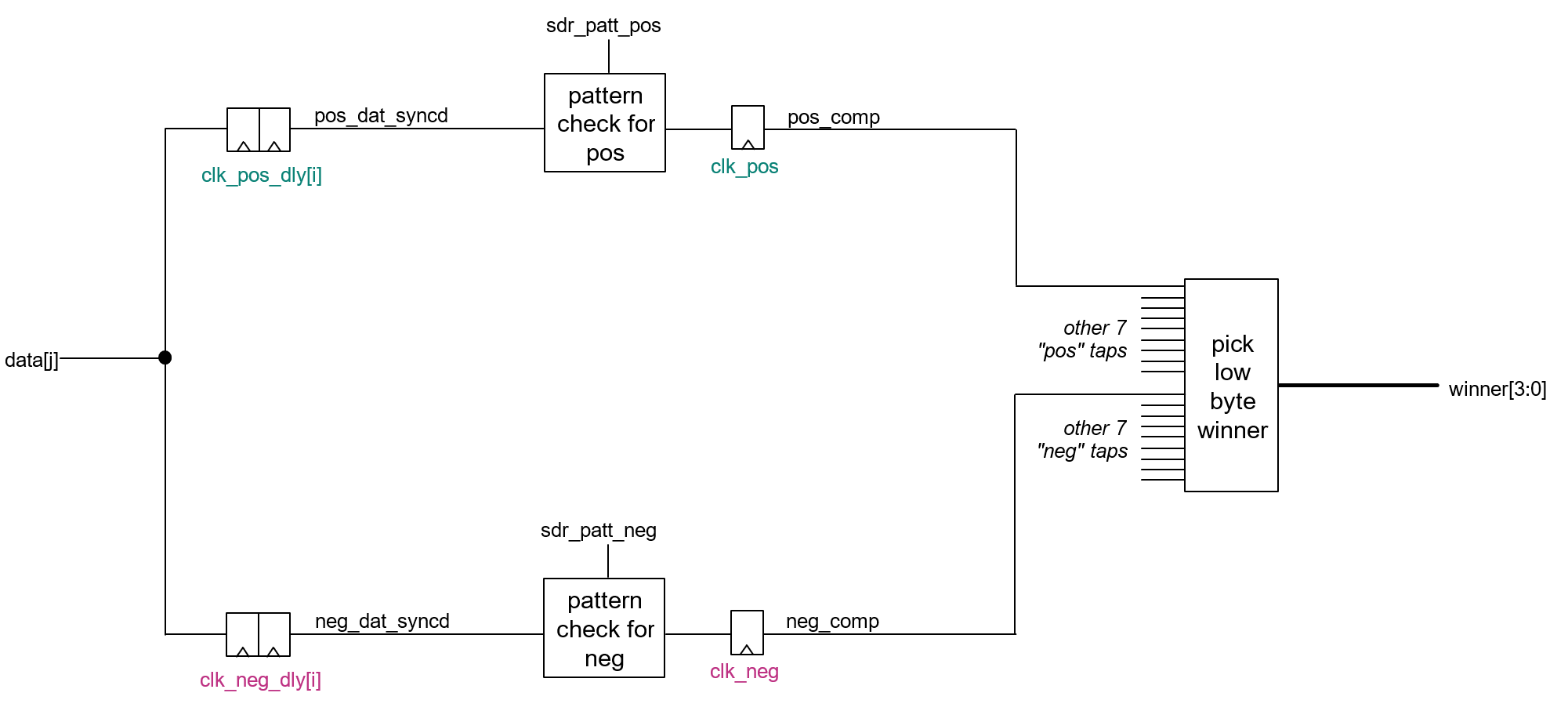
For the “pos” case,
Figure 323
shows the waveforms. Let us assume a 4-bit DLP pattern to keep the comparison short. Note that the data valid window is shown as a full cycle for simplicity, so it does not quite match the tap evaluation example above, which uses a shortened data valid window. Therefore, p7 will be the winner instead of p5, and n5 will be valid instead of invalid by focusing on tap pair 5.
Figure 323.
DLP SDR preamble phase timing, “pos” case
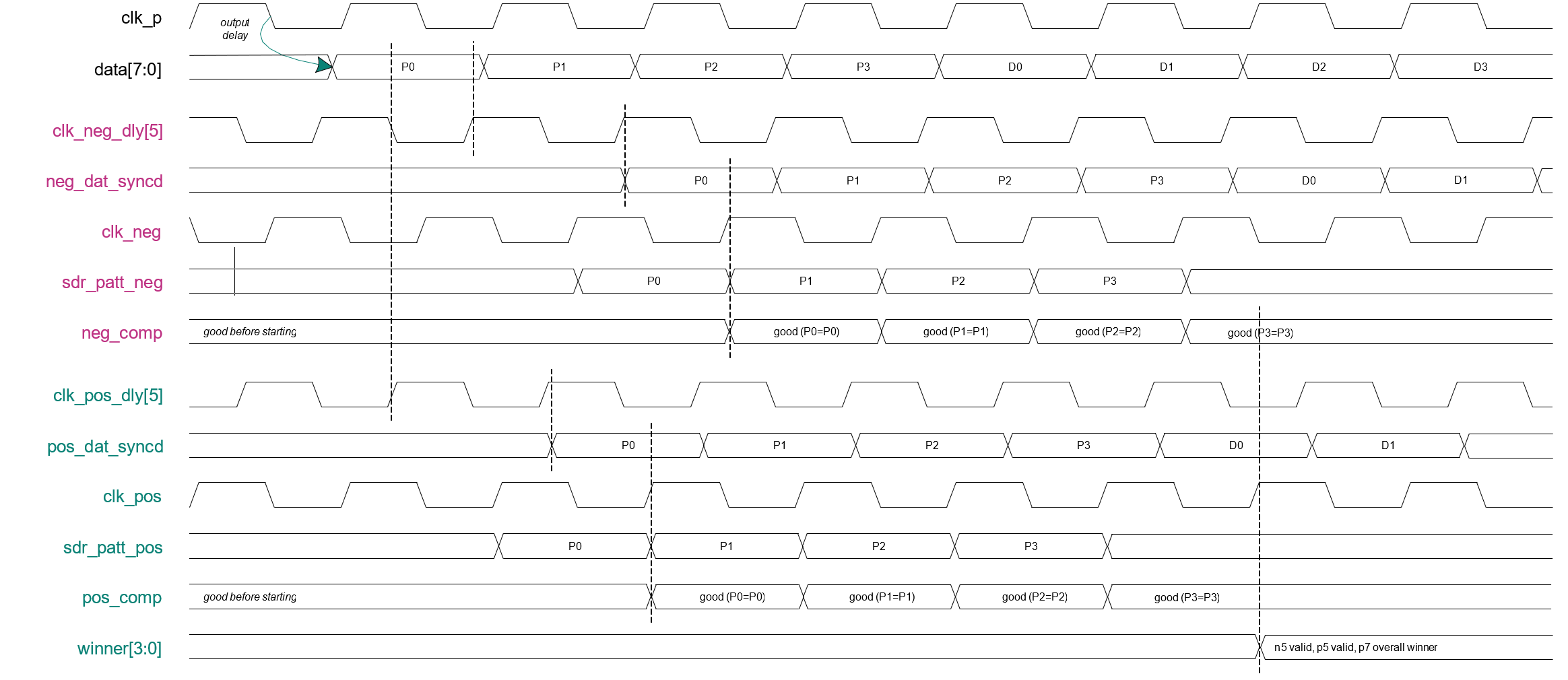
Note that the sdr_pat_* signals serialize differently from DDR.
Figure 324
shows the waveforms for the “neg” case.
Figure 324.
DLP SDR preamble phase timing, “neg” case
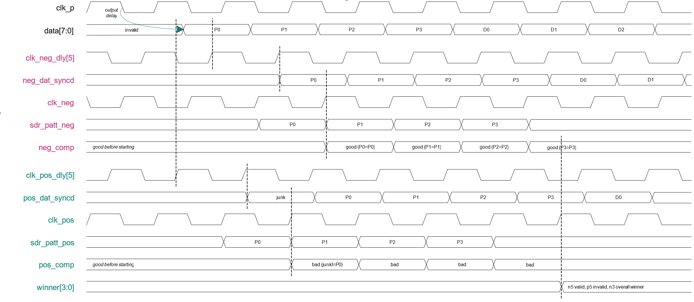
Once the preamble comparison phase is over and the data phase commences, the interface effectively looks like
Figure 325
for the pos case.
Figure 325.
DLP SDR data phase focus, “pos” case
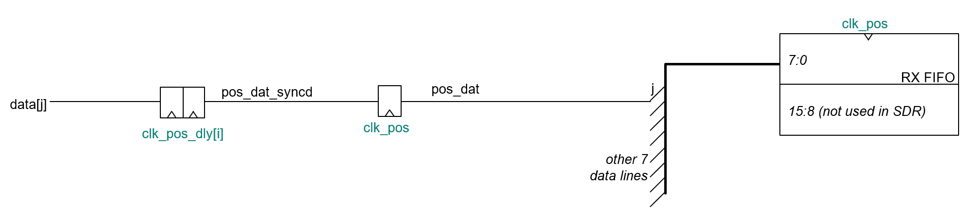
The "pos" case data waveforms are as shown in
Figure 326
for positive tap i, assuming it wins.
Figure 326.
DLP SDR data phase timing, “pos” case
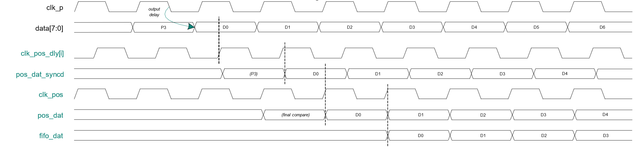
The italicized P3 and “final compare” are only there to show how the comparison phase is finishing, as shown in the previous diagrams; these are not actually captured in the signals shown. For the neg case, the interface effectively looks like
Figure 327
for the data phase.
Figure 327.
DLP SDR data phase focus, “neg” case
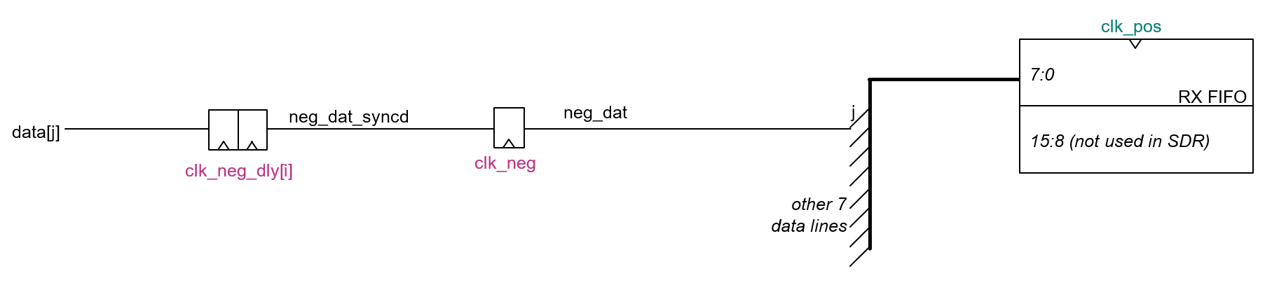
The data phase waveforms for the neg case look like
Figure 328
.
Figure 328.
DLP SDR data phase timing, “neg” case
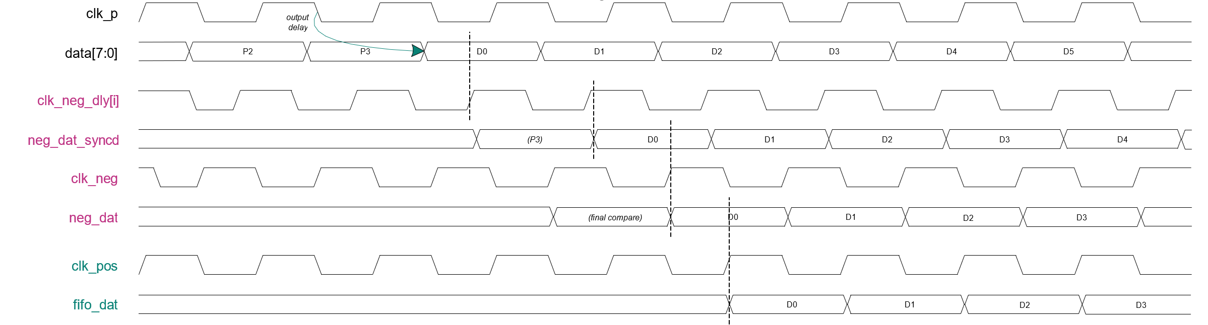
DLL open loop mode
SMIF DLL does not lock to input frequencies below 150 MHz. This means to support memory interface below 75 MHz (in case of CTL2.CLKOUT_DIV = 0) DLL should operate in open loop mode. In open loop mode, DLL does not lock to the frequency of the input clock. Instead, each delay line shifts the clock by a PVT, IDAC and speed mode setting dependent delay.
Open loop mode can be used with SPI SDR, SPI DDR and HYPERBUS™/xSPI modes.
Bypass mode
Bypass mode has been implemented outside of DLL inside SMIF. This mode provides the ability to switch off DLL and use the bypassed clock or inverted bypassed clock to launch the transmit clock and data as well as capture receive data. This optimization improves power consumption in lower frequencies where DLL is not needed.
Bypass mode can be used with SPI DDR and SPI SDR modes. It cannot be used with HYPERBUS™/xSPI DDR mode since the RWDS is used as receive data capture clock. Bypass mode uses the rising or falling edge of the clock without phase shifting. Since RWDS rising and falling edges are outside of the data eye, they cannot be used in bypass mode.
Bypass mode is enabled by setting CTL2.DLL_BYPASS_MODE = 1 and CTL.ENABLED = 1. Bypass mode cannot be used in HB/xSPI DDR mode.
MDL bypass mode
In high-performance modes, the MDL bypass mode can provide an advantage as it bypasses the MDL and therefore uncertainties on the transmit clock are reduced. In this mode PLL jitter and PLL duty cycle distortion contribute to the uncertainties. On the other hand, this mode does not provide the granularity and flexibility which MDL provides. STA results will determine in which modes and frequencies MDL bypass mode is recommended over MDL taps.
MDL bypass mode can be used with SPI SDR, SPI DDR and HYPERBUS™/xSPI modes
Software de-skewing mode
The serial memory devices use a source-synchronous interface where data strobe (RWDS) or output data clock sent by the memories are well aligned with the data used by memory controllers to capture the data.
The standard method of setting the data strobe in the center of the data valid window once at power-up does not always guarantee a robust design as voltage (V) and temperature (T) vary over time.
With higher data rates (i.e 200 MHz, DDR, 400 Mbps (bit period 2,5 ns), the data valid window at the memory controller during the read operation goes down to the 100-200 ps range or there is not even a positive window at all with certain timing uncertainties and variations.
This margin does not provide enough slack to account for VT variations that happen over time, which may cause the data valid window to shift in either direction and at the same time shrink as a percent of the bit period.
Hence there is a need to continuously calibrate the placement of the strobe, such that the strobe is always in the center of the data valid window.
This calibration maximizes the interface performance over all PVT conditions.
The need to place the strobe in the center of the data valid window is most important, but keeping it centered is equally important as voltage (V) and temperature (T) vary over time. Additionally, there is a need to reduce some of these uncertainties and improve the margin on the controller side to achieve and ensure the required performance.
One of the most difficult tasks in designing a memory subsystem is accurately estimating these uncertainties. Timing analysis is typically done by assuming worst case numbers for all parameters. With calibration, the internal timing is set up in real time in a real system environment to achieve optimum timing, highest performance, and a robust design.
The aim of data calibration is to determine and setup the optimum sampling phase of the capture and resynchronization clock.
Figure 329.
Data Valid Window Shifts due to VT Variations
The need to place the strobe in the center of the data valid window is most important, but keeping it centered is equally important as voltage (V) and temperature (T) vary over time. Additionally, there is a need to reduce some of these uncertainties and improve the margin on the controller side to achieve and ensure the required performance.
One of the most difficult tasks in designing a memory subsystem is accurately estimating these uncertainties. Timing analysis is typically done by assuming worst case numbers for all parameters. With calibration, the internal timing is set up in real time in a real system environment to achieve optimum timing, highest performance, and a robust design.
The aim of data calibration is to determine and setup the optimum sampling phase of the capture and resynchronization clock.
Figure 330.
Valid Data Window for 8 Bit Data Interface
Calibration
The calibration can be done either as a "Startup Calibration" or as a "Dynamic Calibration" between certain data transfers phases.
The calibration functionality allows to reduce the data delay uncertainties and to compensate the PVT variations of the critical data path.
There are two ways of calibration:
Startup calibration (eliminates design specific data delay uncertainties). Startup calibration is performed only once at power-up
Dynamic calibration between data transfers (eliminates Temperature variations). Dynamic calibration will be done continuously between defined data transfer phases
Calibration mode
The timing closure is critical for the “HYPERBUS™, xSPI, and Octal SPI w/DQS DDR 200 MHz” protocol, the SMIF has a new capture mode for this particular protocol. This mode is called the “Software de-skewing mode”.
When the software de-skewing mode is enabled, the SMIF logic supports a FW/SW controlled Rx-Capture Clock calibration when configured for “HYPERBUS™, xSPI, and Octal SPI w/DQS DDR” protocol transfers.
With the software de-skewing mode, the SMIF provides a tap delay setting for each bit. The individual data bits can be captured with each of the 16 taps of the slave delay lines. The optimal tap setting for each bit is defined with a FW-controlled calibration sequence. The de-skewing can be done for each data bit for the rising edge of the RWDS signal (clk_pos) and for the falling edge of the RWDS signal (clk_neg). This functionality allows to reduce the data delay uncertainties and to compensate the PVT variations of the critical data path.
Calibration sequence
Once the SMIF initialization is completed, the firmware writes predefined data (training pattern) to the attached memory. Following completion of the training pattern writes and enabling of the firmware Calibration Mode, the firmware starts with the calibration loop.
The SW/FW sets the initial values in the configuration registers for the Software De-skewing Mode to change the tap setting to select the data captured with the selected tap clock. The SW/FW reads the training pattern back from the memory.
The read data is compared against the training pattern written to the memory. Once a training pattern is read, and the comparison operation is complete, and the pass/fail result has been stored, the firmware continues the calibration loop by setting incremental delay values in the configuration registers for the Software De-skewing Mode, reads and compares the data again. This sequence continues until the taps have been swept through all 15 tap delay settings for the rising and falling edge.
The training pattern read comparison is done on a pin-by-pin basis. Once the data read and comparison has been done for all tap settings, the SW/FW calculates the optimal tap delay setting, which places the capture clock in the center of the data valid window and applies this setting to the configuration registers.
Configuration
SMIF provides the configuration register to enable the Software De-skewing Mode and to define the tap selection values for all data bits of all configured memory interfaces
The RX Capture Mode is selected and activated for all connected SMIF memory devices by setting RX_CAPTURE_MODE” in CTL2 Register.
Delay settings for all data bits and devices
The following registers have been added and defined for each of the configured memory devices:
Register: RX_CAPTURE_CONFIG
Bit [8]: FW_CALIBRATION_MODE
Setting: 1: Enabled
Register: HB_FW_DEL_TAP_SEL_0 (HB FW Calibration Delay Tap Select 0)
Bit 31:0: Defines 4 Bit “Tapsel_Pos” setting for Positive Clock and 4 Bit “Tapsel_Neg” for the negative Clock Capture phase.
2 x 4 Bit for Data Bits 0...3
i.e.
Bit [3:0] defines DATA_BIT0_TAP_SEL_POS for Data Bit 0
Bit [7:4] defines DATA_BIT0_TAP_SEL_NEG for Data Bit 0
Register: HB_FW_DEL_TAP_SEL_1 (HB FW Calibration Delay Tap Select 1)
Bit 31:0: defines 4 Bit “Tapsel_Pos” setting for Positive Clock and 4 Bit “Tapsel_Neg” for the negative Clock Capture phase.
2 x 4 Bit for Data Bits 4...7
Bit [3:0] defines DATA_BIT4_TAP_SEL_POS for Data Bit 4
Bit [7:4] defines DATA_BIT4_TAP_SEL_NEG for Data Bit 4
Example for configuration sequence
Configure Memory Interface Protocol:
Configure SMIF for "HYPERBUS™, xSPI, and Octal SPI w/DQS DDR"
Set Rx-Capture Mode:
Navigate to Registers: CTL2
Set RX_CAPTURE_MODE to 2 (for HYPERBUS™/xSPI/Octal SPI w/DQS) by modifying Bits [21:20]
Enable Software De-skewing Mode:
Navigate to Register: RX_CAPTURE_CONFIG
Enable FW_CALIBRATION_MODE by setting Bit [8] to 1
Initialize Memory
Loop from <Start Address> to <End Address>
Write <Pattern> to the <Address space>
Calibration to find optimal Tap Delay settings
//Pseudo Code for Calibration
// Loop through all devices
For i = 0 to 3
Device = i;
// Loop through all Tap Settings
For j = 0 to 15
Tap = j;
// Loop through all Data Bits
For k = 0 to 7
Bit = k;
TapSel_Pos(Bit) = tap;
TapSel_Neg(Bit) = tap;
End // k
// Set Tap delay for Bit 3:0
Write HB_FW_DEL_TAP_SEL_0[Device][31:0] [TapSel_Neg[3], TapSel_Pos[3], ..., TapSel_Neg[0], TapSel_Pos[0]];
// Set Tap delay for Bit 7:4
Write HB_FW_DEL_TAP_SEL_1[Device][31:0] [TapSel_Neg[7], TapSel_Pos[7], ..., TapSel_Neg[4], TapSel_Pos[4]];
// Read predefined data pattern from Address space
Read <Address space>;
// Compare Received Data with Data pattern
// Evaluate each individual Data Bit for each tap setting
End // j
End // i
// Analyze Results and Evaluate Optimal Tap Settings for All Bits
// Set Optimal Tap Values for All Interface Data Bits
For device = 0 to 3
// Set Optimal Tap delay for Bit 7:0
For j = 0 to 7
TapSel_Pos(j) = Opt_TapSel_Pos(j);
TapSel_Neg(j) = Opt_TapSel_Neg(j);
End // j
// Set Optimal Tap delay for Bit 3:0
Write HB_FW_DEL_TAP_SEL_0[Device][31:0] [TapSel_Neg[3], TapSel_Pos[3], ..., TapSel_Neg[0], TapSel_Pos[0]];
// Set Tap delay for Bit 7:4
Write HB_FW_DEL_TAP_SEL_1[Device][31:0] [TapSel_Neg[7], TapSel_Pos[7], ..., TapSel_Neg[4], TapSel_Pos[4]];
End // device
Secure digital host controller (SDHC)
The secure digital host controller (SDHC) in the
PSOC™ Edge E84
MCU allows interfacing with embedded multimedia card (eMMC) - based memory devices, secure digital (SD) cards, and secure digital input output (SDIO) cards. The block supports all the three interfaces - SD, SDIO, and eMMC. The block can also work with devices providing SDIO interface, such as Infineon Wi-Fi products (for example, CYW43439).
illustrates a typical application where there are two SDHC instances, one configured for SD/eMMC to communicate with an SD or eMMC card for mass storage while the other is configured for SDIO to communicate with an Infineon Wi-Fi chip. An example to illustrate this system is an audio application where music is stored locally after retrieving from the internet.
Figure 331.
Typical SDHC application
Features
Complies with eMMC 5.1, SD 6.0 and SDIO 4.10 standards
Supports Host Controller Interface (HCI) 4.2 shared by eMMC and SD
SD interface supports 1-bit and 4-bit bus interfaces, and the following speed modes. The specified data rate is for a 4-bit bus:
3.3-V signal voltage: Default speed (12.5 MB/s at 25 MHz) and High-speed (25 MB/s at 50 MHz)
UHS-I modes using 1.8-V signal voltage : SDR12 (12.5 MB/s at 25 MHz), SDR25 (25 MB/s at 50 MHz), SDR50 (50 MB/s at 100 MHz), and DDR50 (50 MB/s at 50 MHz)
eMMC interface supports 1-bit ,4-bit and 8-bit bus interfaces, and the following speed modes. The specified data rate is for an 8-bit bus
Legacy (26 MB/s at 26 MHz), High-speed SDR (52 MB/s at 52 MHz), and High-speed DDR (104 MB/s at 52 MHz)
Supports three DMA modes - SDMA, ADMA2, and ADMA3 - through a dedicated DMA engine
Supports Command Queuing Engine (CQE)
Provides 2 KB SRAM for buffering up to two 1 KB blocks
Provides I/O interfaces for bus interface voltage selection (3.3 V/1.8 V) and for power enable/disable
Provides I/O interfaces for functions such as card detection, mechanical write protection, eMMC card reset and LED control
Features not supported
The SDHC block does not support the following features:
SD/SDIO operation in UHS-II mode
eMMC boot operation in Dual Data Rate mode
Read wait operation by DAT2 signaling in an SDIO card
Suspend/resume operation in an SDIO card
Interrupt input pins for embedded SD systems
SPI protocol mode of operation
Block diagram
Figure 332.
SDHC Block diagram
The SDHC controller supports all three interfaces - SD, SDIO and eMMC. It supports up to 8-bit bus width. The AHB Master interface helps to transfer data to and fro the system memory and the AHB slave interface provides access to the Configurable registers. The master is security unaware. i.e., it does not generate its own attributes. In order to make it aware of the security, Master Security Controller (MSC) is present between the master port and the AHB bus which controls the access attributes. An asynchronous AHB bridge is present to enable connection to the AHB interconnect which is in different frequency than the AHB master. Command Queuing Engine (CQE) is present between the DMA engine and the Configuration registers. The CQE collects multiple commands and executes in the order of priority which increases the performance.
The register set comprises the standard SD Host Controller Interface (HCI) registers as specified in the SD specifications Part A2 SD Host Controller Standard specification. These registers are described in the
PSOC™ Edge E84
MCU registers reference manual. The DMA engine handles direct data transfer between the SDHC logic and the system memory. It supports SDMA, ADMA2 and ADMA3 modes based on the configuration.
The SDHC block complies with the following standards. For more information on the protocol and operations, see the specifications documents.
SD Specifications Part 1 Physical Layer Specification Version 6.00
SD Specifications Part A2 Host Controller Standard Specification Version 4.20
SD Specifications Part E1 SDIO Specifications Version 4.10
Embedded Multi-Media Card (eMMC) Electrical Standard 5.1
Clocking
lists the different clocks used in the SDHC block. While configuring the clock for SDHC, make sure that CLK_HF1 >= clk_sys >= clk_card.
Source | SDHC clock | Function |
|---|---|---|
Peri 1 Group 0 Clock (CLK_HF1) | AHB bridge clock | Input to the AHB bridge that connects the AHB master interface of the SDHC block to the PERI interconnect that is running at the frequency of CLK_HF1. |
Core SDHC Clock | Used for core SDHC functions including the packet buffer SRAM; it is clocked by the divided output of CLK_HF[i] (clk_sys or clk_peri); | |
AHB Master Interface Clock | Used by the AHB master interface; it is clocked by the divided output of CLK_HF[i] (clk_sys or clk_peri); | |
AHB Slave Interface Clock | Used by the AHB slave interface; it is clocked by the divided output of CLK_HF[i] (clk_sys or clk_peri); | |
Peri m Group n Clock (Peri 1 Group 2 Clock derived from CLK_HF[5] for SDHC0 and Peri 1 Group 3 Clock derived from CLK_HF[6] for SDHC1) | Base Clock/Card Clock | Used for sourcing the SD/eMMC interface clock (clk_card); it is the divided output of Peri m Group n Clock; it must be set to 100 MHz to be compatible with the Capabilities register. See Base clock configuration for details. |
Timer Clock | Used for command and data timeout functions; it is the divided output of Peri m Group n Clock. |
Clock gating
All the clocks except the slave interface clock can be gated internally to enter the Standby mode ( See
Device power modes
). In the Standby mode, the clocks are stopped externally, if required. The slave clock is not gated because it is used for wakeup logic ( Interrupts to CPU ) during the Standby mode.
The card clock is gated by clearing the SD_CLK_EN bit and other clocks are gated by clearing the INTERNAL_CLK_EN bit of the CLK_CTRL_R register. See
Clock setup
for the sequence to be followed while modifying the bit.
Base clock configuration
The HCI register (Capabilities) has a read-only field (BASE_CLK_FREQ) to indicate the base clock frequency so that an SD HCI-compatible driver can easily configure the divider for the required bus speed. This value is set to '0x64' (100 MHz) and hence the divided output of Peri m Group n Clock is set to 100 MHz. If this compatibility is not required, the divided output of Peri m Group n Clock can be set to any value. See
Timeout (TOUT) configuration
.
Card clock (SDCLK) configuration
The SDCLK or card clock frequency is set by configuring the 10-bit divider in the CLK_CTRL_R register and selecting the 10-bit divided Clock mode by clearing the CLK_GEN_SELECT bit of the same register. The default value of this bit is '0'. The UPPER_FREQ_SEL field holds the upper two bits (9:8) and the FREQ_SEL field holds the lower eight bits (7:0) of the divider. The base clock frequency is sourced from the divided output of Peri m Group n Clock as explained in
Table 396
. SDCLK frequency is equal to base clock frequency when the divider value is zero.
SDCLK frequency = Base clock frequency / (2 x 10-bit divider value)
These fields are set automatically, based on the selected Bus Speed mode, to a value specified in one of the preset registers when HOST_CTRL2_R.PRESET_VAL_ENABLE is set. The preset registers are selected according to
Table 397
.
Timeout (TOUT) configuration
An internal timer is used for the command and data timeouts. The timeout value is specified through the TOUT_CTRL_R.TOUT_CNT register field. The timer clock (TMCLK) frequency indicated by the read-only fields TOUT_CLK_FREQ and TOUT_CLK_UNIT of CAPABILITIES1_R register is 1 MHz. The timer clock is derived by dividing the divided output of Peri m Group n Clock, which means that the divided output of Peri m Group n Clock must be set to 100 MHz to be compatible with the Capabilities register.
Bus Speed modes
The SDHC block can operate in either SD/SDIO mode or in eMMC mode. The SDHC block operates in eMMC mode when the EMMC_CTRL_R.CARD_IS_EMMC bit is set; otherwise, it operates in SD/SDIO mode. The Speed mode is configured through HOST_CTRL1_R and HOST_CTRL2_R registers as per
Table 397
. The HOST_CTRL2_R.UHS2_IF_ENABLE bit should remain at its default value of '0' because the block does not support UHS-II mode. The card clock must be configured according to the selected Speed mode through the CLK_CTRL_R register. See
Card clock (SDCLK) configuration
for more information.
Bus Speed mode | HOST_CTRL1_R field | HOST_CTRL2_R fields | Selected Preset register | |
|---|---|---|---|---|
HIGH_SPEED_EN | SIGNALING_EN | UHS_MODE_SEL | ||
SD Default Speed (DS) | 0 | 0 | Don't care | PRESET_DS_R |
SD High- speed (HS) | 1 | 0 | Don't care | PRESET_HS_R |
SDR12/eMMC Legacy | Don't care | 1 | 000b | PRESET_SDR12_R |
SDR25/eMMC High- speed | Don't care | 1 | 001b | PRESET_SDR25_R |
SDR50 | Don't care | 1 | 010b | PRESET_SDR50_R |
DDR50/eMMC High- speed DDR | Don't care | 1 | 100b | PRESET_DDR50_R |
Power modes
The block can operate during the Active and Sleep system power modes. It does not support Deep Sleep mode and cannot wake up from events such as card insertion and removal when the system is in Deep Sleep. All the core registers except the packet buffer SRAM are retained when the system enters Deep Sleep mode and the SRAM is switched OFF to save power. Retention is performed, so that the block can resume operation immediately after wakeup from the Deep Sleep without reconfiguration. Ensure that no AHB traffic ( such as Register Read/Write and DMA operation) is present, the SD/SDIO/eMMC bus interface is idle, and no data packets are pending in the packet buffer SRAM when the system transitions into Deep Sleep mode. The control information is stored in the SRAM, as the CQE is present,. Hence Command Queue tasks should also be emptied from SRAM before entering Deep Sleep mode.
Standby mode
The block can be put into Standby mode to save power during the Active and Sleep system power modes by turning OFF the clocks. See
Clock gating
for more details. The block can detect wakeup interrupts (
Interrupts to CPU
) in the Standby mode.
Interrupts to CPU
The block provides two interrupt signals to CPUSS:
Wakeup interrupt signal - Triggered on events such as card insertion , removal, and SDIO card interrupt. This interrupt source cannot wake up the system from the Deep Sleep mode and is provided so that a host driver can take appropriate action on those events. For example, resuming operation from the Standby mode on card insertion. See Standby mode for more details. The card insertion and removal is not applicable to an embedded device, wakeup interrupt is not used. However, it can still be used for SDIO card interrupt
General interrupt signal - Triggered on all other events, in either normal conditions or error conditions
A host driver must not enable the wakeup and general interrupt signals at the same time.
To use only the wakeup interrupt signal, clear the NORMAL_INT_STAT_R and NORMAL_INT_SIGNAL_EN_R registers, and then set the enable bits of the required wakeup events in the WUP_CTRL_R and NORMAL_INT_STAT_EN registers.
To use only the general interrupt signal, clear the WUP_CTRL_R and NORMAL_INT_STAT_R registers. Then, set the required bits in NORMAL_INT_SIGNAL_EN_R and NORMAL_INT_STAT_EN registers.
These interrupts remain asserted until the CPU clears the interrupt status through one of the status registers - NORMAL_INT_STAT_R and ERROR_INT_STAT_R.
The SDIO card interrupt status bit, CARD_INTERRUPT, is a read-only bit. The host driver may clear the NORMAL_INT_STAT_EN_R.CARD_INTERRUPT_STAT_EN bit before servicing the SDIO card interrupt and may set this bit again after all interrupt requests from the card are cleared to prevent inadvertent interrupts.
shows the list of registers used in interrupt configuration.
Register | Description |
|---|---|
WUP_CTRL_R | Enables or disables different wakeup interrupts. Host driver must maintain voltage on the SD bus by setting PWR_CTRL_R.SD_BUS_PWR_VDD1 bit for these interrupts to occur. These interrupts cannot wakeup the device from the Deep Sleep. |
NORMAL_INT_STAT_R | Reflects the status of wakeup interrupts and non-error general interrupts. It also has a bit to indicate whether any of the bits in ERROR_INT_STAT_R is set. |
ERROR_INT_STAT_R | Reflects the status of general interrupts that are triggered by error conditions. |
NORMAL_INT_STAT_EN_R | Provides mask bits for wakeup interrupts and non-error general interrupts. |
ERROR_INT_STAT_EN_R | Provides mask bits for general interrupts that are trigerred by error conditions. |
NORMAL_INT_SIGNAL_EN_R | Setting any of these bits to '1' enables interrupt generation for wakeup interrupts and non-error general interrupts. |
ERROR_INT_SIGNAL_EN_R | Setting any of these bits to '1' enables interrupt generation for general interrupts that are triggered by error conditions. |
FORCE_ERROR_INT_STAT_R | Forces an error interrrupt to occur when the corresponding bit is set. |
SDIO interrupt
The SDIO interrupt function is supported on card_dat_3to01 line (SD pin 8). See the SDIO specifications for more details on this feature. The CARD_INTERRUPT_STAT_EN bit in the NORMAL_INT_STAT_EN_R register and the CARD_INTERRUPT_SIGNAL_EN bit in the NORMAL_INT_SIGNAL_EN_R register must be set to enable this interrupt. To use this interrupt as wakeup interrupt, use WUP_CTRL_R.WUP_CARD_INT instead of NORMAL_INT_SIGNAL_EN_R.
I/O interface
The SDHC block provides the signals shown in
Table 399
, which can be routed to pins through the I/O subsystem (IOSS).See
I/O Subsystem
to configure the I/Os, and the datasheet for specific pins available for each signal. The SDHC also supports SDIO interrupt on DAT1 line (card_data_3to01). The output signals must be configured in Strong Drive mode, bi-directional signals in strong drive with the input buffer ON, and the input pins in Hi-Z mode when an external pull-up resistor is available; otherwise, they must be configured in internal pull-up mode. The input buffer must be enabled for input pins. The drive mode of the DAT lines must be set to Hi-Z after card removal. See
Card detection
for more details. In addition to configuring the Drive mode and HSIOM registers in IOSS, the SDHC_CORE.GP_OUT_R register must be configured to enable the required signals. See
Table 399
. The card_detect_n and card_write_prot should be connected to ground if an eMMC or an embedded SDIO device is connected.
Signal | Function | Register configuration |
|---|---|---|
clk_card | Clock output | GP_OUT_R.CARD_CLOCK_OE |
card_cmd | Command (bi-directional) | Always enabled |
card_dat_3to0[3:0] | Data (bi-directional) | HOST_CTRL1_R.DAT_XFER_WIDTH |
card_detect_n | Card detect signal input, Active LOW | GP_OUT_R.CARD_DETECT_EN |
card_mech_write_prot | Mechanical write protect signal input, Active LOW | GP_OUT_R.CARD_MECH_WRITE_PROT_EN |
io_volt_sel | Signaling voltage select output (see Switching signaling Voltage from 3.3 V to 1.8 V section) | GP_OUT_R.IO_VOLT_SEL_OE |
card_if_pwr_en | Card interface power enable output | GP_OUT_R.CARD_IF_PWR_EN_OE |
Switching signaling Voltage from 3.3 V to 1.8 V
The I/Os operate at the voltage level supplied through the external VDDIO pin. The SD mode supports switching the signaling voltage from 3.3 V to 1.8 V after negotiation with the SD card. The block sets the HOST_CTRL2_R.SIGNALING_EN bit to indicate the switch. This value is reflected on the io_volt_sel pin, which is connected to an external regulator powering VDDIO to switch between 3.3 V and 1.8 V.
Note:
PSOC™ Edge E84
MCU does not provide an internal regulator to power the SD interface I/Os.
Packet buffer SRAM
SRAM that is internal to the SDHC block is used as a packet buffer to store data packets while carrying out data transfer to and from the card. The size of the SRAM is 2 KB to support buffering of two 1- KB blocks. Also an additional 128 bytes are available for command queuing. The write and read transfers to the cards do not occur simultaneously, a single shared buffer is used to read and write operations. During the data transfer command handshake, the read or write bit of the Command register is sampled and stored. This internal bit defines whether the SDHC is in Read or Write mode.
shows how data flows from the card interface to the AHB master interface through the packet buffer for a card read transfer. The data received from the card interface is written into packet buffer. When one block of data is received, DMA starts transmitting that data to the system by reading it from the packet buffer. For a card write transfer, data flows in the reverse direction. DMA writes data into a packet buffer that is subsequently read by the card interface logic. The DMA and card interface logic can work simultaneously because read and write to packet buffer can be interleaved. For card read, DMA can send out the previous block while card interface logic is receiving the current block. For card write, DMA can write the current block into packet buffer while card interface logic is sending out for the previous block.
Figure 333.
Data flow in a read transfer
Packet buffer full or empty
When the packet buffer becomes full in card read, the clock to the card is stopped to prevent the card from sending the next data block. When packet buffer is empty, data block is not sent. In both the cases, card interface logic is IDLE. The SDHC does not support SDIO Read Wait Signalling through DAT2. Therefore, the I/O command (CMD52) cannot be performed during multiple read cycle because the card clock is stopped.
DMA engine
DMA engine handles the data transfer between SDHC and system memory. Following are the features of this unit:
Supports SDMA, ADMA2, and ADMA3 modes based on the configuration
The same DMA engine is used to interleave data transfer and descriptor fetch. This enables new task descriptor fetches (for CMD44 and CMD45) while DMA is moving data during task execution (for CMD46 and CMD47)
Prefetches data for back-to-back eMMC Write commands
Writes back the received data packets to the system memory
shows the data flow between the host driver and the SD bus. The host driver can transfer data using either a programmed I/O (PIO) method in which the internal buffer is accessed through the Buffer Data Port (BUF_DATA_R) register or using any of the defined DMA methods. The PIO mode is slow and burdens the processor. Do not use the PIO mode for large transfers.
Figure 334.
Data flow
DMA supports both single block and multi-block transfers. The control bits in the Block Gap Control (BGAP_CTRL_R) register is used to stop and restart a DMA operation. The SDMA mode is used for short data transfer because it generates interrupts at page boundaries. These interrupts disturb the CPU to reprogram the new system address. For every SDMA operation, only one SD command transaction is executed.
ADMA2 and ADMA3 are used for long data transfers. They adopt scatter gather algorithm so that higher data transfer speed is available. The host driver can program a list of data transfers between system memory and SD card to the descriptor table. ADMA2 performs one read or write SD command operation at a time. ADMA3 can program multiple read or write SD command operation in descriptor table.
In the SDMA and ADMA2 modes, writing the CMD_R register triggers the DMA operation. In ADMA3 mode, writing ADMA_ID_LOW_R register triggers the DMA operation.
The SD mode commands are generated by writing into the following registers - system address (SDMASA_R), block size (BLOCKSIZE_R), block count (BLOCKCOUNT_R), transfer mode (XFER_MODE_R), and command (CMD_R). When HOST_CTRL2_R.HOST_VER4_EN=0, SDMA uses SDMASA_R as system address register and hence Auto CMD23 is not used with SDMA because the register is assigned as a 32-bit block count for Auto CMD23 . When HOST_CTRL2_R.HOST_VER4_EN=1, SDMA uses ADMA_SA_LOW_R as system address register and SDMASA_R is reassigned to 32-bit block count and hence SDMA uses Auto CMD23.
To use the 32-bit block count register when HOST_CTRL2.HOST_VER4_EN=1, it must be programmed with a non-zero value and the value of the 16-bit block count register BLOCK_COUNT_R must be '0'.
See the respective specifications documents listed in
Figure 332
for more information about DMA operation.
Initialization sequence
shows the sequence for initializing the SDHC to work with SD/SDIO/eMMC cards. Subsequent sections describe each step. After initialization, the SDHC is ready to communicate with the card. See the corresponding specifications document for information on other sequences such as card initialization and identification, changing Bus Speed mode, signal voltage switch procedure, transaction generation, and an error recovery.
Figure 335.
SDHC programming sequence
Enabling SDHC
Ensure clk_sys is configured to be greater than or equal to clk_card and is running. Then, follow the sequence in
Figure 336
to enable the block. The internal clock can also be enabled later the clock setup. It must be enabled to detect card insertion or removal through general interrupts when SDHC is not in the Standby mode. See
Card detection
for more details.
Figure 336.
SDHC enable sequence
Card detection
Ensure the card is already inserted by following the sequence in
Figure 337
.This step is required for a removable card. After the card is detected , the host driver can supply power and clock to the card. If the card is inserted, then proceed with SDHC initialization. To detect card insertion or removal through interrupt when the internal clock is already enabled, follow the sequence shown in
Figure 338
. To detect the card status through interrupt when the internal clock is disabled (when SDHC is in the Standby mode), the bits in the WUP_CTRL_R register are cleared. See
Interrupts to CPU
for more details. To detect SDIO card interrupt on DAT1 line, a separate bit is provided in these registers, which must be configured.
SDHC clears the PWR_CTRL_R.SD_BUS_PWR_VDD1 bit when the card is removed and drives the DAT lines LOW. Therefore , the drive mode of the DAT lines must be changed from STRONG (with input buffer ON) to HI-Z when the card is removed to keep the lines pulled HIGH. After detecting card insertion, the drive mode must be configured back to STRONG (with input buffer ON) mode only after PWR_CTRL_R.SD_BUS_PWR_VDD1 is set to '1'.
Figure 337.
Card status check sequence
Figure 338.
Card detection through interrupt
SDHC initialization
To initialize SDHC, configure the basic settings as shown in
Figure 339
.This step is executed immediately after enabling SDHC.
Figure 339.
SDHC setup
Clock setup
Enable the internal clock followed by the card clock (SD clock) by following the sequence shown in
Figure 340
. The SD clock frequency must be 100 kHz to 400 KHz during the card initialization. See
Card clock (SDCLK) configuration
for more details. The SD clock is started and stopped by toggling the CLK_CTRL_R.SD_CLK_EN bit. The same sequence excluding the step of enabling the internal clock is used to change the SD clock frequency. The SD clock is stopped before changing its frequency. Note that GP_OUT_R.CARD_CLOCK_OE should be set to '1' for the card clock to appear on the pin.
Figure 340.
SDHC clock setup
Error detection
SDHC can detect different types of errors in the SD and eMMC transactions. An Error is detected in either the command or data portion of the transaction. When an error is detected, the ERR_INTERRUPT bit in the NORMAL_INT_STAT_R register is set. The exact error can then be identified through the ERROR_INT_STAT_R register. The Abort command is used to recover from an error detected during data transfer. In addition to these two registers, SDHC has two other error status registers - Auto CMD Error Status (AUTO_CMD_STAT_R) and ADMA Error Status (ADMA_ERR_STAT_R). The following table lists the errors detected by SDHC.
Type | Error |
|---|---|
Command errors | Command timeout error Command CRC error Command End Bit error Command Index error Command Conflict error Response error |
Auto Command errors | Command not issued by Auto CMD12 Error Auto command timeout error Auto command CRC Error Auto command End Bit error Auto command index error Auto command conflict error Auto CMD response Error |
Data errors | Data timeout error Data CRC error Data end bit error ADMA error Tuning error |
Registers summary
Some important SDHC registers are listed below. For mode details, see Register reference manual.
Symbol | Register name | Description |
|---|---|---|
SDMASA_R | SDMA System Address Register | Configures a 32-bit Block Count or an SDMA system address-based on the Host v4 Enable bit in the Host Control 2 register. |
BLOCKSIZE_R | Block Size Register | Configures an SDMA buffer boundary and the number of bytes in a data block. |
BLOCKCOUNT_R | 16-bit Block Count Register | Configures the number of data blocks. |
XFER_MODE_R | Transfer Mode Register | Controls the operation of data transfers for an SD/eMMC mode. |
CMD_R | Command Register | Provides the information related to a command and a response packet. |
HOST_CTRL1_R | Host Control Register | Controls the operation of the Host Controller. |
HOST_CTRL2_R | ||
PWR_CTRL_R | Power Control Register | Controls the power of the Card. |
CLK_CTRL_R | Clock Control Register | Controls SDCLK (card clock) in an SD/eMMC mode. |
EMMC_CTRL_R | eMMC Control Register | Controls eMMC operation |
BGAP_CTRL_R | Block Gap Control Register | Used by the host driver to control any operation related to block gap. |
WUP_CTRL_R | Wake Control Register | Wakesup an idle Host driver. |
Universal serial bus - high speed (USBHS)
Note:
The portions of USBHS section copyrighted ©2023 by Synopsys, Inc. All rights reserved. Used with permission.
The USB high speed (USBHS) block is designed to enable fast data transfers of up to 480 Mbps. It comprises of a USB controller (USB CTRL) and USB physical layer (USB PHY) and can act as either a host or device at a particular time. It is compliant with the USB 2.0 specification, including provision for device enumeration, configuration, and control, as well as data transfer mechanisms such as bulk, interrupt, and isochronous transfer modes.
Features
Complies with USB 2.0 specification
Can be configured as USB Host or USB Device (one at a time)
Supports the following speed modes:
High-speed (HS): 480 Mbps
Full-speed (FS): 12 Mbps
Low-speed (LS): 1.5 Mbps [only as host]
Supports up to 9 bidirectional endpoints (EP0 - EP8), where EP0 is a control endpoint and EP1 to EP8 are data endpoints
Supports up to 16 host channels
Supports AHB5 master and slave interface for accessing the data FIFO, queues, and its Memory Mapped Input/Output (MMIO) control and status registers, respectively
Supports all 4 types of USB data transfers (control, bulk, isochronous, and interrupt)
Includes a dedicated Scatter/Gather DMA interface to avoid using CPU for packet transfers
Includes a 6912x35-KB SRAM buffer for both Host and Device mode operations
Supports high-bandwidth multimedia, isochronous data transfers that can store up to 3*1 KB packet per endpoint
Supports remote wakeup, host, or device-initiated resumes
Supports Link Power Management (LPM) suspend and sleep modes
Architecture
illustrates the architecture of the USBHS block. It consists of the USB physical layer (USB_PHY), the USB controller (USB_CTRL), and the USBHS subsystem (USBHSSS) integration components.
Figure 341.
USBHS block diagram
USB physical layer
The USB PHY allows physical layer communication between the USB device and USB host through the DP and DM pins. It handles low-level USB protocol and signaling and supports SYNC detection, data serialization and deserialization, and data recovery.
The USB PHY consists of three basic components: the common block, transceiver block, and the VREG block.
Common block
The USB PHY common block contains circuitry that provides biasing and reference clocks for each transceiver block. It contains the phase-locked loop (PLL), Bias, and REFCLK_LOGIC blocks.
The PLL takes a reference clock from the REFCLK_LOGIC block and outputs equally-spaced (in time) phases that are propagated to the digital core.
The bias block provides bias references to the analog circuitry in both the command and transceiver blocks.
The REFCLK_LOGIC block performs all mode control, multiplexing, and division of core clock sources.
Transceiver
The USB PHY transceiver block contains circuitry for data processing and transfers. It comprises of a digital core and analog block, which control the transmit, receive, disconnect detection, squelch detection, and automatic tuning functions.
The transmitter block contains drivers for all three speed modes in the USB protocol: HS mode at 480 Mbps, FS mode at 12 Mbps, and LS mode at 1.5 Mbps. That includes automatically tuning the input and output impedance based on the speed.
Internal 1.8-V regulator
The Vreg18 block is an internal 1.8-V regulator that generates a 1.8-V supply for the USB PHY.
USB Controller
The USB Controller is responsible to interface the USB PHY through the USB Transceiver Macro-cell Interface (UTMI+). The CPU has no direct access to the USB PHY. All interfacing with the USBHS goes through its 32-bit AHB5 Master for data transfer and to the System Peripheral Interconnect (SPERI) through AHB5 Slave for both subsystem-level MMIO and the USB Controller’s internal Control and Status (CSR) registers programming.
AHB bus interface unit
There are two AHB buses to interface the USB controller and USB subsystem:
AHB5 master interface:
It operates typically at 400 MHz, which is the native speed of the APPCPUSS. The signals are synchronized to 100 MHz internally, as the USB controller operates at 100 MHz to reduce area and power consumption. The AHB5 Master interface supports only non-sequential transactions as the bridge supports only non-sequential transactions.
AHB5 slave interface:
It operates typically at 100 MHz from SPERI. It interfaces with the MMIO registers of the USB controller and USB subsystem
Control and status registers
The control and status registers (CSR) block resides in the AHB clock domain (100 MHz) and incorporates most of the MMIO registers related to the USB controller. The AHB5 slave interface unit can write and read registers, and the USB controller can set or reset the interrupt and status bits.
Application interface unit
The application interface unit (AIU) is responsible for the following functions:
Generating and writing the delimiter (byte enables and last DWORD indicator) into the transmit FIFOs (based on the FIFO number) for transmit packets in Device (IN) and Host (OUT) modes
Writing a token into the request queue (periodic/non-periodic) for transmit transactions in Device and Host modes
Writing a token into the Request Queue for receive (IN) transactions (only in Host mode)
Selecting the periodic or non-periodic request queue based on the type of transaction. The periodic queue is selected when the channel or endpoint indicates the type of transaction.
Generating interrupts for both transmit and receive operations in Device and Host modes
Address decoding for selecting the appropriate transmit FIFOs and queues
Generating DMA interface signals to access an internal DMA controller for data transfers
Round-robin arbitration among periodic and non-periodic channels and endpoints. Higher priority is always given to periodic channels or endpoints
Transmit/receive threshold handling when Tx thresholding is enabled
Rewinding logic for DMA address and transfer size during an Underrun/Overflow condition when thresholding is enabled
Packet FIFO controller
Several FIFOs are used in Device and Host modes to store data inside the controller before transmitting it on either the AHB or the USB. The FIFOs can store periodic and non-periodic transmit data. The FIFOs are configured to be dedicated to an endpoint.
It also manages the interface to a single-port synchronous SRAM. The address, write data, and control outputs are driven by this block.
Media access controller
The Media access controller (MAC) module handles USB transactions. It performs the following functions:
Handles the speed enumeration, suspend, resume, and remote wakeup functions
Responsible for token, data, and handshake packet generation and reception, and PID and CRC checking and generation
Tracks SOF packets and generates SOF interrupts in Device mode
In Host mode, it is responsible for connect and disconnect detection and USB reset
Converts data widths for the 8-bit PHY interface and multiplexes output signals to the PHY from multiple blocks
PHY interface unit
This block manages the connection between the USB controller and USB PHY through the UTMI+ interface.
Wake-up and power controller
When the USB is suspended or the session is not valid, the PHY is driven into suspend mode and the PHY clock is stopped to reduce PHY and USB controller power consumption. To reduce power consumption further, the USB controller also supports AHB clock gating and partial power-down.
USB subsystem
The USB subsystem is responsible to connect the USB controller with other parts of the device, such as the APPCPUSS, SRSS and SPERI.
AHB interface
The SPERI provides a 32-bit AHB5 slave interface for MMIO register access.
The APPCPUSS provides an 8/32-bit AHB5 master interface for data transfer between the application and USB.
Refer to the
AHB bus interface unit
section for additional description.
Qchannel
Qchannel interface is a simple handshake between APPCPUSS and the USBHS subsystem via SPERI for power or clock controlling.
Clock and resets
The USBHS controller typically runs at 100 MHz. This clock can be synchronized internally from a 400-MHz clock from SRSS.
The block also has an asynchronous active low asserted reset at the 100-MHz clock domain with synchronous de-assertion.
Interrupts
The USBHS controller has one synchronous level sensitive, active high interrupt. None of the interrupts from the USBHS subsystem are used.
Operation
Subsystem modes
The USB subsystem can be configured either in device or host mode. This is controlled by the USB_MODE bit of the SUBSYSTEM_CTL register. This bit should be set HIGH for host mode and LOW for device mode.
The SS_ENABLE bit from SUBSYSTEM_CTL register indicates if the USBHS block is enabled or disabled. The USBHS block shall be only enabled when both analog and digital power supplies, all the high frequency clocks, and reset signals are stable.
Clocking settings
When the device core operates in high-performance mode at 0.9V, the USB controller typically runs at 100-MHz clock. This clock can be derived from the 400 MHz from APPCPUSS (CLK_HF1). If the CLK_HF1 is set to 100 MHz, it does not require any synchronization. The AHB_MASTER_SYNC bit of the SUBSYSTEM_CTL register enables/disables the synchronization with the CLK_HF1. Set this bit LOW to disable synchronization (when CLK_HF1 = 100 MHz) and HIGH to enable it (when CLK_HF1 = 400 MHz).
When the device core operates in low-power mode at 0.8V, the clock frequencies are scaled down by 2.5, and hence the USB subsystem will operate at 40 MHz. The CLK_HF1 can also be scaled down from 400 MHz to 160 MHz.
When the device core operates in ultra low power mode at 0.7V, the USBHS block cannot operate.
The USB PHY requires a PLL reference clock frequency (CLK_HF8), which has to be set to 9.6, 10, 12 or 50 MHz through the PLL_FSEL bits from the PHY_FUNC_CTL_1 register. If the PLL_B_TUNE bit is set HIGH, the three first frequencies can be tuned to double their value to 19.2, 20 and 24 MHz. The current version of this hardware only allows a 50-MHz PLL reference clock frequency; therefore, the PLL_FSEL and PLL_B_TUNE must be set to 3'b111 and 1'b0, respectively.
The 50-MHz PLL reference shall have a tolerance of +/-400 ppm, a peak jitter of +/-100 ps, duty cycle between 40/60 and 60/40 at 0.9V nominal. A few possible combinations to achieve such accuracy are:
ECO > PLL250 > CLK_HF8
ECO > PLL500 > CLK_HF8
EXTCLK > CLK_HF8
Reset recovery
The USB recovery can be initiated by the USB controller using the PORT_RESET bit from the PHY_FUNC_CTL_1 register at any point of time during the normal mode of operation: transmission or reception. On its assertion, the PHY’s transmit and receive logic are reset while the PLL remains locked to ensure synchronization with the USB controller.
The only requirement is that within 100 ns of PORT_RESET assertion, the USB controller should set PHY inputs appropriately to bring the latter into a safe status as follows:
When a host, set the SUBSYSTEM_CTL.USB_MODE to 1’b1 and set DCTL.SftDiscon to 1’b1
When a device, set the SUBSYSTEM_CTL.USB_MODE to 1’b0 and set DCTL.SftDiscon to 1’b1
The PORT_RESET de-assertion is equally important and should meet the following required conditions:
On reception, a minimum of 150 µs after asserting PORT_RESET
On transmission, a minimum of 150 µs after the DCTL.SftDiscon is set to 1’b1
Note:
PORT_RESET is generally used in multi-port applications. Its usage requires enough statistics for the USB controller and/or subsystem to initiate the reset.
When the USB controller throws multiple packet error interrupts, after polling its status registers, memory should be forced to flush, disable the USB subsystem through the SS_ENABLE bit. Then re-enable it and reconfigure the required controller registers.
PHY tuning
The USB PHY uses an internal resistor method to calibrate the DP and DM 45-Ω source impedance. The RES_TUNING_SEL and EFUSE_SEL bits from PHY_FUNC_CTL_2 should always be set to 1’b1. The RES_TUNING_CODE will be set based on the impedance measured during bench testing. Its value will be enforced automatically during boot time. The user shall not change the value of this field.
Other tuning settings shall be kept to their default values:
Bits from PHY_FUNC_CTL_1 | Default values |
|---|---|
DISCONNECT_THRESHOLD | 3’b011 (0%) |
SQUELCH_THRESHOLD | 3’b010 (0%) |
CHARGER_TYPE_DETECTION | 2’b01 (0%) |
TX_HS_CROSSOVER | 2’b11 (0mV) |
FS_LS_SOURCE_IMPENDANCE | 4’b0011 (0%) |
HS_DC_VOLTAGE | 4’b0011 (0%) |
HS_TX_RISETUNE | 2’b01 (0%) |
USB_SOURCE_IMPEDANCE | 2’b01 (0 Ohms) |
HS_TX_PRE_EMPHASIS_CURRENT | 2’b00 (0) |
HS_TX_PRE_EMPHASIS_DURATION | 1’b0 (2x long pre-emphasis) |
PLL_I_TUNE | 2’b00 (1x) |
Interrupt settings
The current interrupt registers from the USBHS subsystem, including the INTR_SS, INTR_SS_SET, INTR_SS_MASK and INTER_SS_MASKED registers, are unused. Use the GINTSTS register for system-level events in the current mode (Device or Host mode). Use the GINTMSK register to mask the desired interrupt events.
Controller initialization
If the cable is connected during power-up, the current mode of operation bit in the Controller Interrupt register (GINTSTS.CurMod) reflects the mode. The USB controller enters Host mode when an "A" plug is connected, or Device mode when a "B" plug is connected.
This section explains the initialization of the USB controller after power-on. The application must follow this initialization sequence irrespective of whether the USB controller is going to be configured in Host or Device mode of operations. All controller global registers are initialized according to the controller's configuration. The parameters referred to in this section are the USBHS configuration parameters defined in the USBHS chapter in the
PSOC™ Edge E84
MCU Registers Reference manual.
Read the User Hardware Configuration registers (GHWCFG1, 2, 3, and 4) to find the configuration parameters selected for the USB controller
Program the following fields in the Global AHB Configuration (GAHBCFG) register
DMA Mode bit
AHB Burst Length field
Global Interrupt Mask bit = 1
Program the following field in the Global Interrupt Mask (GINTMSK) register
GINTMSK.RxFLvIMsk = 1'b0
Program the following fields in the GUSBCFG register.
The USB turnaround time (USBTrdTim) field
HS/FS TimeOUT time-out calibration (TOutCal) field
The software must unmask the following bits in the GINTMSK register
OTG Interrupt Mask
Mode Mismatch Interrupt Mask
The software can read the GINTSTS.CurMod bit to determine whether the USB controller is operating in Host or Device mode. The software then follows either the Host or Device initialization
Note:
The controller is designed to be interrupt-driven. The polling interrupt mechanism is not recommended as this may result in undefined resolutions.
Note:
In device mode, just after Power-On Reset or a Soft Reset, the GINTSTS.Sof bit is set to 1'b1 for debug purposes. This status must be cleared and can be ignored.
Data FIFO RAM allocation
If Dynamic FIFO sizing is enabled in the controller, the external RAM must be allocated among different FIFOs in the controller before any transactions can start. The application must follow this procedure every time it changes the controller FIFO RAM allocation.
The application must allocate data RAM per FIFO based on the following criteria:
AHB's operating frequency
PHY clock frequency
Available AHB bandwidth
Performance required on the USB
Based on the above criteria, the application must provide a table with RAM sizes for each FIFO. The USBHS block shares a single SPRAM between transmit FIFO(s) and receive FIFO.
In the Scatter Gather DMA mode, the base descriptor address, the current buffer address, and the descriptor status quadlet information for each endpoint/channel are stored in the SPRAM. This register information is stored at the end of the SPRAM after the space allocated for receive and Transmit FIFO. These register space must also be taken into account when calculating the total FIFO depth of the controller.
In addition, the DIEPDMAn/DOEPDMAn registers are maintained in RAM regardless of using Dynamic FIFO sizing.
Use the rules listed in
Table 403
to calculate the RAM space that must be allocated to store these registers.
Mode | RAM space allocation |
|---|---|
Host | Four locations per channel as follows:
|
Device | Four locations per endpoint direction as follows:
|
Device mode RAM allocation
The considerations for allocation of data RAM for Device Mode FIFO are listed here:
Receive FIFO RAM allocation
RAM for SETUP packets: 10 locations must be reserved in the RxFIFO to receive a SETUP packet on the control endpoint. The controller does not use these locations, which are Reserved for SETUP packets, to write any other data
One location for Global OUT NAK
Status information is written to the FIFO along with each received packet. Therefore, a minimum space of (Large Packet Size/4)+1 must be allotted to receive packets. If a high-bandwidth endpoint is enabled, or multiple isochronous endpoints are enabled, then at least two (Largest Packet Size/4)+1 spaces must be allotted to receive back-to-back packets. Typically, two (Largest Packet Size/4)+1 spaces are recommended so that when the previous packet is being transferred to AHB, the USB can receive the subsequent packet. If AHB latency is high, you must allocate enough space to receive multiple packets. This is critical to prevent dropping of any isochronous packets
Along with the last packet of each endpoint, information on transfer complete status is also pushed in to the FIFO
An additional location for EPDisable status for each endpoint is also required
Typically, two locations for each OUT endpoint is recommended
Transmit FIFO RAM allocation
The minimum RAM space required for each IN endpoint Transmit FIFO is the maximum packet size for the particular IN endpoint
More space allocated in the transmit IN endpoint FIFO results in a better performance on the USB and can hide latencies on the AHB
FIFO name | Data RAM size |
|---|---|
Receive data FIFO | rx_fifo_size. This must include RAM for setup packets, OUT endpoint control information and data OUT packets |
Transmit FIFO 0 | tx_fifo_size0 |
Transmit FIFO 1 | tx_fifo_size1 |
Transmit FIFO 2 | tx_fifo_size2 |
... | ... |
Transmit FIFO i | tx_fifo_size[i] |
With this information, program the following registers:
Receive FIFO Size register (GRXFSIZ)
GRXFSIZ.Receive FIFO depth = rx_fifo_size;
Device IN endpoint transmit FIFO0 size register (GNPTXFSIZ)
GNPTXFSIZ.non-periodic transmit FIFO depth = tx_fifo_size0;
GNPTXFSIZ.non-periodic transmit RAM start address = rx_fifo_size;
Device IN endpoint transmit FIFO#1 size register (DIEPTXF1)
DIEPTXF1.Transmit RAM start address = GNPTXFSIZ.FIFO0.Transmit RAM start address + tx_fifo_size0;
Device IN endpoint transmit FIFO#2 size register (DIEPTXF2)
DIEPTXF2.Transmit RAM start address = GNPTXFSIZ.FIFO1.Transmit RAM start address + tx_fifo_size1;
Device IN endpoint transmit FIFO#i size register (DIEPTXFi)
DIEPTXFi.Transmit RAM start address = GNPTXFSIZ.FIFOi-1.Transmit RAM start address + tx_fifo_size[i-1];
The TxFIFOs and the RxFIFO must be flushed after the RAM allocation is done, for proper functioning of the FIFOs
GRSTCTL.TxFNum = 5'h10
GRSTCTL.TxFFlush = 1'b1
GRSTCTL.RxFFlush = 1'b1
The application must wait until the TxFFlush bit and the RxFFlush bits are cleared before performing any operation on the controller
Host mode RAM allocation
The considerations for allocating data RAM for Host Mode FIFOs are listed here:
Receive FIFO RAM allocation
Status information is written to the FIFO along with each received packet. Therefore, a minimum space of (Largest Packet Size/4)+2 must be allotted to receive packets. If a high-bandwidth channel is enabled, or multiple isochronous channels are enabled, then at least two (Largest Packet Size/4)+2 spaces must be allotted to receive back-to-back packets. Typically, two (Largest Packet Size/4)+2 spaces are recommended so that when the previous packet is being transferred to AHB, the USB can receive the subsequent packet. If AHB latency is high, you must allocate enough space to receive multiple packets
Along with each host channel's last packet, information on transfer complete status and channel halted is also pushed to the FIFO. So two locations must be allocated for this
Transmit FIFO RAM allocation
The minimum amount of RAM required for the host non-periodic transmit FIFO is the largest maximum packet size among all supported non-periodic OUT channels
More space allocated in the Transmit non-periodic FIFO results in better performance on the USB and can hide AHB latencies. Typically, two largest packet sizes' worth of space is recommended, so that when the current packet is under transfer to the USB, the AHB can get the next packet. If the AHB latency is large, then you must allocate enough space to buffer multiple packets
The minimum amount of RAM required for host periodic transmit FIFO is the largest maximum packet size among all supported periodic OUT channels. If there is at least one high-bandwidth isochronous OUT endpoint, then the space must be at least two times the maximum packet size of that channel
Internal register storage space allocation
When operating in Scatter/Gather DMA mode, four locations per channel must be reserved
Table 405.
Host mode FIFO and RAM size
FIFO name
Data RAM size
Receive Data FIFO
rx_fifo_size
Non-periodic transmit FIFO
tx_fifo_size0
IN endpoint transmit FIFO
tx_fifo_size1
With this information, program the following registers:
Receive FIFO size register (GRXFSIZ)
GRXFSIZ.RxFDep = rx_fifo_size;
Non-periodic transmit FIFO size register (GNPTXFSIZ)
GNPTXFSIZ.NPTxFDe = tx_fifo_size0;
GNPTXFSIZ.NPTxFStAddr = rx_fifo_size;
Host periodic transmit FIFO size register (HPTXFSIZ)
The TxFIFOs and RxFIFO must be flushed after RAM allocation for proper FIFO functioning
GRSTCTL.TxFNum = 5'h10
GRSTCTL.TxFFlush = 1'b1
GRSTCTL.RxFFlush = 1'b1
The application must wait until the TxFFlush bit and the RxFFlush bits are cleared before performing any operating on the controller
Host programming overview
This section discusses how to program the USBHS block when it is in Host mode.
Host initialization
To initialize the controller as host, the application must perform the following steps.
Program GINTMSK.PrtInt to unmask
Program the HCFG register to select full-speed host or high-speed host
Program the HPRT.PrtPwr bit to 1'b1. This drives VBUS on the USB
Wait for the HPRT.PrtConnDet interrupt. This indicates that a device is connected to the port
Program the HPRT.PrtRst bit to 1'b1. This starts the reset process
Wait at least 10 ms for the reset process to complete
Program the HPRT.PrtRst bit to 1'b0
Wait for the HPRT.PrtEnChng interrupt
Read the HPRT.PrtSpd field to get the enumerated speed
Program the HFIR register with a value corresponding to the selected PHY clock
32
Program the RXFSIZE register to select the size of the RxFIFO
Program the GNPTXFSIZ register to select the size and the start address of the non-periodic transmit FIFO for non-periodic transactions
Program the HPTXFSIZ register to select the size and start address of the periodic transmit FIFO for periodic transactions
To communicate with devices, the application must initialize and enable at least one channel, as described in
Initializing channels
.
Host connection
The following steps explain the host connection flow:
When the USB cable is plugged to the Host port, the controller triggers the GINTSTS.ConIDStsChng interrupt
When the Host application detects the GINTSTS.ConIDStsChng interrupt, the application can turn on VBUS by setting HPRT.PrtPwr = 1'b1
The PHY indicates VBUS power-on by asserting utmi_vbusvalid
When the Host controller detects the device connection, it triggers the host port interrupt (GINTSTS.PrtInt) to the application
When GINTSTS.PrtInt is triggered, the application reads the HPRT register to check if the HPRT.PrtConnDet (port connect detected) bit is set or not
Host disconnection
The host disconnect flow is as follows:
When the device is disconnected from the USB cable (but the cable is still connected to the USB host), the controller triggers the GINTSTS.DisconnInt (Disconnect Detected) interrupt
Note:
If the USB cable is disconnected from the Host port without removing the device, the controller generates an additional interrupt - GINTSTS.ConIDStsChng (Connector ID status change)
The controller does not switch off VBUS because the VBUS is controlled externally
Initializing channels
The application must initialize one or more channels before it can communicate with connected devices. To initialize and enable a channel, the application must perform the following steps.
Program the periodic frame list array (for periodic channels)
Program the HFLBAddr register with the base address of the periodic frame list array (for periodic channels)
Program the HCFG register with PerSchedEn bit set
Program at least one transfer descriptor in the system memory
Program the HCDMAn with the pointer to the corresponding descriptor
Program the GINTMSK register to unmask the channel interrupts
Program the HAINTMSK register to unmask the selected channels' interrupts
Program the HCINTMSK register to unmask the ChHalt, XferCompl, and BNA
Program the HCTSIZn register with initial data PID and SCHED_INFO (for periodic channels)
Program the HCCHARn register with the device's endpoint characteristics, such as type, speed, direction, and so on (the channel can be enabled by setting the channel enable bit to 1'b1 only when the application is ready to transmit or receive any packet)
Halting a channel
The application can disable any channel by programming the HCCHARn register with the HCCHARn.ChDis and HCCHARn.ChEna bits set to 1’b1. This enables the USB host to flush the posted requests (if any) and generates a channel halted interrupt. The application must wait for the HCINTn.ChHltd interrupt before reallocating the channel for other transactions. The USB host does not interrupt the transaction that has already started on the USB.
The controller generates a RxFLvl interrupt when there is an entry in the queue. The application must read/pop the GRXSTSP register to generate the channel halted interrupt.
To disable a channel in the DMA mode operation, the application does not have to check for space in the request queue. The USB host checks for space in which to write the disable request on the disabled channel’s turn during arbitration. Meanwhile, all posted requests are dropped from the request queue when the HCCHARn.ChDis bit is set to 1’b1.
The application is expected to disable a channel under any of the following conditions:
When a GINTSTS.DisconnInt (Disconnect device) interrupt is received. The application must check for the HPRT.PrtConnSts, because when the device directly connected to the host is disconnected, HPRT.PrtConnSts is reset. The application must issue a soft reset to ensure that all channels are cleared. When the device is reconnected, the host must issue a USB reset
When the application aborts a transfer before normal completion
Host descriptor memory structures
In the scatter/gather DMA mode, the controller implements a true scatter-gather memory distribution in which data buffers are scattered over the system memory. However, the descriptors themselves are continuous. Each channel memory structure is implemented as a contiguous list of descriptors; each descriptor points to a data buffer of a predefined size. In addition to the buffer pointer (1 DWORD), the descriptor also has a status quadlet (1 DWORD). When the list is implemented as a ring buffer, the list processor switches to the first element of the list when it encounters the last bit. All channels (control, bulk, interrupt, and isochronous) implement these structures in memory.
Note:
The descriptors are stored in continuous locations. For example, descriptor 1 is stored in 32’h0000_0000, descriptor 2 is stored in 32’h0000_0008, descriptor 3 in 32’h0000_0010, and so on. The descriptors are always DWORD aligned
The descriptor memory structures are displayed in
Figure 342
Figure 342.
Descriptor memory structures
All channels must implement the following memory structure:
Each channel has one memory structure
Each data buffer must have a descriptor associated with it to provide the status of the buffer. The buffer itself contains only raw data
Each buffer descriptor is two quadlets long. When the descriptor is ready, the DMA fetches and processes its data buffer. The buffers to which the descriptor points hold packet data for non-isochronous channels and packet data corresponding to the frame (FS)/microframe (HS) data for isochronous channels
The handshake between the application and controller is accomplished by the Active bit field in the status quadlet of the descriptor as described below:
A = 1 indicates that the descriptor is ready
A = 0 indicates that the descriptor is not ready
The IN and OUT data memory structures and the definition of status quadlet bits for non-ISO and ISO channels. are shown in
Figure 343
.
Figure 343.
Memory structure
In addition, a frame list in memory for isochronous and interrupt channels contains information on the channels that need to be scheduled in a frame. For periodic channels, the USBHS block reads the list corresponding to the frame number and schedules the channel that has Ch_sch = 1 in the appropriate frame.
Figure 344.
Frame list for periodic channels
IN memory structure
All channels that support IN direction transactions (channels that receive data from the USB device) must implement a memory structure with the following characteristics:
Each data buffer must have a descriptor associated with it to provide the status of the buffer. The buffer itself contains only raw data
Each buffer descriptor is two quadlets long
displays the IN data memory structure fields.
Bit | Bit ID | Description | |
|---|---|---|---|
A 31 | Active bit | This 1-bit value indicates whether the descriptor is ready. For non-isochronous channels, this bit indicates the following:
For isochronous channels, this bit indicates the following:
The application sets this bit when the descriptor is ready. The USB block resets this bit while closing the descriptor. The application needs to set this bit as a last step after the entire descriptor is ready. The controller resets this bit as a final step of processing the descriptor. This bit is accessed by both the controller and the application | |
Rx sts 29:28 | Receive status | This 2-bit field describes the status of the received data. The controller updates this field when the descriptor is closed. PKTERR is set by the controller when there was an error while receiving the packet. When updated with PKTERR, it is an indication that IN data has been received with errors. The error includes Xact_err scenarios. BUFERR is set by the controller when AHB error is encountered during buffer access. The possible combinations are:
This field has to be initialized to 2’b00 by the application and updated by the controller subsequently | |
EoL [26] | End of List | For non-isochronous, it indicates that this is the last descriptor in the list, if set. The controller does not generate a BNA interrupt for the next descriptor, if it is unavailable. For isochronous, this field is reserved. This field is controlled by the application | |
IOC [25] | Interrupt on complete | Set by the application, this bit indicates that the controller must generate a transfer complete interrupt (XferCompl) after this descriptor is finished | |
[24] † | † Varies | Non-isochronous reserved | Isochronous Bit: [24:23] |
[23] † | † Varies | Non-isochronous IN Bit: [23] Bit ID: AQTD_VALID Alternate Queue Transfer Descriptor Valid. When set by the application, if a short packet is received, the controller jumps to a new descriptor in the same list. The new descriptor address is obtained by replacing the CTD value of the corresponding channel with the AQTD value. When the application resets this bit, the controller ignores AQTD. | Bit ID: R: reserved |
[22:17] † | † Varies | Non-isochronous IN Bit: [23] Bit ID: AQTD_VALID Alternate Queue Transfer Descriptor Valid. This is valid only if AQTD_VALID is set. This field gives the offset value in DWORDS. The controller will use this offset to jump to a new descriptor address in the same list. | Isochronous IN bit Bit: [22:12] Bit ID: R reserved |
[16:12] † | † Varies | Non-isochronous IN | |
[11] † | † Varies | Bit: [16:0] Bit ID: Total bytes to transfer This 17-bit value can take values from 0 to 128K-1 bytes, depending on the transfer size of data received from the USB device | Isochronous IN Bit: [11:0] Bit ID: received |
[10:0] † | † Varies | The application programs the expected transfer size. When the descriptor is closed, this indicates remainder of the transfer size. This field must be in multiple of MPS for the corresponding end point. The MPS for various packet types are as follows:
| Isochronous IN Bit: [11:0] Bit ID: Total bytes to transfer This 11-bit value can take values from 0 to 4K bytes, depending on the packet size of data received from the USB host. The application programs the expected transfer size. When the descriptor is closed, it indicates remainder of the transfer size. The maximum payload size of each ISO packet as per USB specification 2.0 is as follows.
Note: A value of 0 indicates zero bytes of data, 1 indicates 1 byte of data, and so on. |
Following is the OUT buffer pointer field description: | |||
Buf addr 31:0 | Buffer address | The buffer pointer field in the descriptor is 32 bits wide and contains the address where the received data is to be stored in the system memory. | |
† The meaning of this field varies. See description. | |||
OUT memory structure
All channels that support OUT direction transactions (channels that transmit data to the USB device) must implement the following memory structure:
Each buffer must have a descriptor associated with it
The application fills the data buffer, updates its status in the descriptor, and enables the channel
The DMA fetches this descriptor and processes it, moving on in this manner until it reaches the end of the descriptor chain
The buffer to which the descriptor points to hold packet data for non-isochronous channels and frame (FS)/microframe (HS) data for isochronous channels.
displays the OUT data memory structure fields.
Bits that are not present are reserved to be set to zero by the application for writes and ignored during reads.
Bit | Bit ID | Description | |
|---|---|---|---|
A 31 | Active bit | This 1-bit value indicates whether the descriptor is ready. For non-isochronous channels, this bit indicates the following:
For isochronous channels, this bit indicates the following:
The application sets this bit when the descriptor is ready. The USB block resets this bit while closing the descriptor. The application needs to set this bit as a last step after the entire descriptor is ready. The controller resets this bit as a final step of processing the descriptor | |
Tx sts 29:28 | Transmit status | The status of the transmitted data. This reflects if the OUT data has been transmitted correctly or with errors. BUFERR is set by the controller when there is an AHB error during buffer access along with asserting the AHBERR interrupt (HCINTn register) for the corresponding channel. PKTERR is set by the controller when there is an error while transmitting the packet. The error includes Xact_err scenarios. Following are the possible combinations:
This field has to be initialized to 2’b00 by the application and updated by the controller subsequently. | |
EoL [26] | End of list | For non-isochronous, it indicates that this is the last descriptor in the list, if set. The controller does not generate a BNA interrupt for the next descriptor, if it is unavailable. For isochronous, this field is reserved. This field is controlled by the application. | |
IOC [25] | Interrupt on complete | Set by the application, this bit indicates that the controller must generate a transfer complete interrupt after this descriptor is finished. | |
[24] † | SuP | Non-isochronous OUT Setup packet When set, it indicates that the buffer data pointed by this descriptor is a setup packet of 8 bytes | Isochronous Reserved: [24:12] |
[24] † | R | Non-isochronous OUT Bit: Reserved [23] Bit ID: Reserved | |
[22:17] † | † Varies | Non-isochronous OUT Bit: Reserved [22:17] Bit ID: Reserved | |
[16:12] † | † Varies | Non-isochronous OUT Bit: Reserved [16:0] Bit ID: Total bytes to transfer This 17-bit value can take values from 0 to 128K-1 bytes, indicating the number of bytes of data to be transmitted to the USB device. Note: A value of 0 indicates zero bytes of data, 1 indicates 1 byte of data and so on. | |
[11:0] † | † Varies | Isochronous OUT Bit: [11:0] Bit ID: Total bytes to transfer This 12-bit value can take values from 0 to 4K bytes, indicating the number of bytes of data to be trv Note: A value of 0 indicates zero bytes of data, 1 indicates 1 byte of data, and so on. | |
Following is the OUT buffer pointer field description: | |||
Buf addr 31:0 | Buffer address | The buffer pointer field in the descriptor is 32 bits wide and contains the address where the transmit data is to be stored in the system memory. | |
† The meaning of this field varies. See description. | |||
Asynchronous transfers
When the application enables an asynchronous (bulk and control) channel by writing into the HCCHARn register, the host controller begins servicing the asynchronous channel. It reads the referenced (CTD) transfer descriptor qTDn (pointed to by the HCDMAn register). If the read qTDn is active, the host controller caches the qTDn and then schedules a transaction. If the read qTDn is inactive, the host controller disables the channel and generates a Buffer Not Available (BNA) interrupt.
If multiple asynchronous channels are enabled simultaneously, the host controller caches the referenced transfer descriptor of the entire enabled channels. The host controller schedules transactions for each enabled channel in round-robin fashion.
When the host controller completes the transfer for a channel, it updates the status quadlet of the processed qTDn in the system memory.
For a normal completion, the host controller updates the qTDn status with no errors. The host controller completes a transfer normally if one of the following events occurs:
Short or zero-length packet is received for an IN channel
The allocated buffer is fulfilled with the received data packets for an IN channel
The allocated buffer is fully transferred to the device for an OUT channel
When a transfer is completed normally, the host controller attempts to process the next qTDn from the descriptor list, if the End of List (EOL) bit is not set in the completed qTDn.
where m = AQTD (if IN channel with AQTD_VLD = 1 received a short packet) or m = (n + 1) mod (NTD + 1)
If EOL is set, the host controller disables the channel and generates a Channel Halt interrupt. The transfer complete interrupt is generated for the following conditions.
IOC is set
Short or zero-length packet is received for an IN channel
EOL is set
For an abnormal completion, the host controller updates the status of the qTDn with PKT_ERR. The host controller completes a transfer abnormally if one of the following events occurs:
STALL response is received from the device
Excessive transaction errors occurred
Babble detected
When a transfer completes abnormally, the host controller disables the channel and then generates a channel halt interrupt with the appropriate status in the HCINT register.
Asynchronous transfer descriptor
The application must use separate qTD for different stages of control transfers. A three-stage control transfer uses three qTDs. The same qTD can be reused for performing different stages of control transfer. The combination of EPType, EPDir fields of the HCCHARn register, and the SuP flag of the qTD decides the stage of the control transfer. See
Table 408
.
HCCHARn.EP Type | HCCHARn.EP Dir | qTD.SuP | Control Stage |
|---|---|---|---|
2'b00 | 0 | 1 | SETUP |
2'b00 | 0 | 0 | Data stage OUT/Status stage OUT |
2'b00 | 1 | 0 | Data stage IN/Status stage IN |
2'b00 | 1 | 1 | Invalid |
The host controller executes a zero-length OUT transaction if the “Num bytes to transfer” field of the qTD is initialized to zero for an OUT channel. For an IN channel, the “Num of bytes received” field of the qTD must be always initialized to an integer multiple of the maximum packet size.
The application can use one or multiple qTDs for bulk IN and OUT transfers. The number of qTDs depends on the available consecutive data buffer space and the size of the transfer. Each qTD can support up to 64KB of consecutive data buffer space.
The host controller handles the ping protocol when it operates in high speed.
Periodic transfers
The periodic schedule is used to manage all isochronous and interrupt transfer streams. The base of the periodic schedule is the periodic frame list. The periodic schedule is referenced from the register space using the HFLBAddrBase and the HFNUM registers. The periodic schedule is based on an array of scheduled channels called the periodic frame list. The periodic frame list implements a sliding window of transactions over time. When the application enables the periodic schedule (PerSchedEna) in the HCFG register, the host controller attempts to read an entry from the frame list that corresponds to the next running frame number at the beginning of each frame.
The periodic frame list can be programmed to 8, 16, 32, or 64 elements. The size of the periodic frame list should be large enough to support the required b-interval of the least frequent channel. The least significant bits 15:0 in the periodic frame list elements are used to identify the scheduled periodic channels (0 through 15) for that corresponding frame. For example, if channel 2 and 6 are periodic channels scheduled for a frame, then the corresponding entry in the periodic frame list will be 32’h0000_0044.
For high speed, the host controller uses SCHED_INFO of the HCTSIZn register as a sliding window for micro-frame scheduling within the scheduled frame (periodic frame list). Even though the micro-frame scheduling is done through the descriptor list, SCHED_INFO is used to restrict the descriptor fetches for isochronous channels.
The host controller should program the SCHED_INFO to 8’b1111_1111 when operating in full speed for all the enabled periodic channels.
Isochronous transactions
When the application enables an isochronous channel by writing into the HCCHARn register, the host controller begins servicing the isochronous channel based on the programmed scheduling (periodic frame list and SCHED_INFO). The application must use a separate qTD for each micro-frame (or frame for FS). Each qTD handles a micro-frame (or frame in FS) of transactions. The application is expected to allocate a qTD with active bit zero even if no transaction is scheduled for a micro-frame (or frame). The position of the active qTD determines the b-interval of the isochronous channel.
The host controller supports high-bandwidth isochronous transfer via the multi-count (MC) field of the HCCHARn register. The multi-count represents a transaction count per micro-frame for the endpoint. If the multi- count is zero, the operation of the host controller is undefined. Multi-count greater than one is not applicable for the FS host.
For OUT transfers, the value of the “Num bytes to transfer” field represents the total bytes to be sent during the micro-frame. The application is expected to program the multi-count field to be the maximum number of packets to be sent in any micro-frame. The host controller automatically selects the number of packets and its data PID based on the programmed Xfer size.
For IN transfers, the host controller issues multi-count transactions. The application is expected to initialize the “Num bytes received” field to (MC * MaxPktSize).
The host controller does not execute all multi-count transactions if:
The channel is an OUT and the “Num bytes to transfer” field goes to zero before all the multi-count transactions have executed (ran out of transmit data) or
The channel is an IN and the endpoint delivers a short packet, or an error occurs on a transaction before all the multi-count transaction have been executed
The channel is an IN and the endpoint delivers a packet with DATA0 PID before all the multi-count transaction have been executed
Each transfer descriptor (qTD) describes one micro-frame (HS) or one frame of transactions. The host controller will cache one transfer descriptor in a micro-frame (or frame) prior to the scheduled micro-frame (or frame).
When the application is adding new isochronous transactions to the schedule, it always performs a read of the HFNUM register to determine the current frame and micro-frame the host is currently executing. Because there is no information about where in the micro-frame (or frame) the host controller is, a constant uncertainty factor of one micro-frame for HS and one frame for FS is assumed.
The end of micro-frame (HS) or frame (FS) may occur before all of the transaction opportunities are executed. When this happens, the host controller closes the corresponding descriptor and proceeds to processing the next scheduled descriptor. If the scheduled descriptor is not fetched by the host controller due to high system latency, the host controller does not execute any transaction for that scheduled micro-frame (or frame) and will skip the descriptor without any update (that is, without clearing the active bit).
When a transfer is completed normally, the host controller generates the transfer complete interrupt only if IOC is set in the completed qTD.
When a transfer is completed abnormally (STALL response or Babble), the host controller disables the channel and then generates a channel halt interrupt with the appropriate status in HCINT register. The host controller updates the status of the qTD with PKT_ERR if one of the following conditions occurs:
STALL response is received from the device
Error packet received
Babble detected
Unable to complete all the transactions in the scheduled micro-frame/frame
An example for the HS isochronous scheduling is shown in
Figure 345
. In this figure, channels 2 and 15 are isochronous channels with b-intervals of 125μs and 4ms respectively. The host controller fetches only the qTDs that correspond to the SCHED_INFO within the scheduled frame (Periodic Frame List entry). The host controller initiates the qTD fetch in the micro-frame prior to the scheduled micro-frame. If the qTD is active and belongs to an OUT channel, the host controller also fetches the corresponding data in the previous micro-frame. If this qTD is not active, the host controller ignores the qTD and does not generate any BNA interrupt.
Figure 345.
High-speed isochronous transfer scheduling
Interrupt transactions
When the application enables an interrupt channel by writing into the HCCHARn register, the host controller begins servicing the interrupt channel based on the programmed scheduling (periodic frame list and SCHLD_INFO). It reads the referenced (CTD) transfer descriptor qTDn (pointed by the HCDMAn register) in the micro-frame (or frame for FS) prior to the scheduled micro-frame (or frame).
If the read qTDn is active, the host controller caches the qTDn and then schedules a transaction. If the read qTDn is inactive, the host controller disables the channel and generates a Buffer Not Available (BNA) interrupt.
When the host controller completes the transfer, it updates the status quadlet of the processed qTDn in the system memory.
For a normal completion, the host controller updates the status of the qTDn with no errors. The host controller completes a transfer normally if one of the following events occurs:
Short or zero length packet is received for an IN channel
The allocated buffer is fulfilled with the received data packets for an IN channel
The allocated buffer is fully transferred to the device for an OUT channel
When a transfer completes normally, the host controller attempts to process the next qTDm from the descriptor list if the End of List (EOL) bit is not set in the completed qTDn.
Where m = (n + 1) mod (NTD + 1)
If EOL is set, the host controller disables the channel and generates a channel halt interrupt. The transfer complete interrupt will be generated for the following conditions.
IOC is set
Short or zero length packet is received for an IN channel
EOL is set
For an abnormal completion, the host controller updates the status of the qTDn with PKT_ERR. The host controller completes a transfer abnormally if one of the following events occurs:
STALL response is received from the device
Excessive transaction errors occurred
Babble detected
When a transfer completes abnormally, the host controller disables the channel and then generates a channel halt interrupt with the appropriate status in the HCINT register.
The host controller supports a high-bandwidth interrupt transfer through the multi-count (MC) field of HCCHARn register. The multi-count represents a transaction count per micro-frame for the endpoint. If the multi-count is zero, the operation of the host controller is undefined. Multi-count greater than one is not applicable for FS host.
The host controller does not execute all multi-count transactions in a micro-frame if:
The channel is an OUT and the “Num bytes to transfer” field goes to zero before all the multi-count transactions have executed (ran out of transmit data) or
The channel is an IN and the endpoint delivers a short packet, or an error occurs on a transaction before all the multi-count transaction have been executed
The channel is an IN and the “Num bytes received” goes to zero before all the multi-count transaction are executed (ran out of receive buffer space)
Device programming overview
This section discusses how to program the USBHS block when it is in Device mode.
Device initialization
As prerequisites, the application must set up the device controller to handle traffic by masking the GINTMSK.NPTxFEmpMsk and GINTMSK.RxFLvlMsk interrupts.
The application must perform the following steps to initialize the controller at device on, power on, or after a mode change from Host to Device.
Program the following fields in the DCFG register:
DescDMA bit
Device speed
Non-zero length status OUT handshake
Periodic frame interval
Inter-packet gap ISOC OUT worst-case support (ipgisocSupt)
Clear the DCTL.SftDiscon bit. The controller issues a connect after this bit is cleared
If the device is using ADP probing, wait for 20 PHY clocks and activate PMU GPWRDN.PMUActiv =1'b1
Program the GINTMSK register to unmask the following interrupts:
USB reset
Enumeration done
Early suspend
USB suspend
SOF
Wait for the GINTSTS.USBReset interrupt, which indicates a reset has been detected on the USB and lasts for about 10 ms. On receiving this interrupt, the application must perform the steps listed in
Initialization on USB reset
At this point, the device is ready to accept SOF packets and perform control transfers on control endpoint 0.
Device connection
If VBUS is on when the device is connected to the USB cable, the device connection flow is as follows:
The device triggers the GINTSTS.SessReqInt [bit 30] interrupt bit
When the device application detects the GINTSTS.SessReqInt interrupt, it programs the required bits in the DCFG register
When the Host drives Reset, the Device triggers GINTSTS.USBRst [bit 12] on detecting the reset. The host then follows the USB 2.0 enumeration sequence
If VBUS is off when the device is connected to the USB cable, the device needs to wait till VBUS is on.
Device disconnection
The device session ends when the USB cable is disconnected or if the VBUS is switched off by the Host. The device disconnect flow is as follows:
When the USB cable is unplugged or when the VBUS is switched off by the Host, the device controller triggers GINTSTS.USBRst [bit 12] interrupt bit
When the device application detects GINTSTS.USBRst, the application sets a time-out check for SETADDRESS Control Xfer from the Host
If the application does not receive SET ADDRESS Control Xfer from the Host before the time-out period, it is treated as a device disconnection
Device soft disconnection
The application can also perform a soft disconnect by setting the soft disconnect bit (SftDiscon) in the device control register (DCTL). The sequence of operations depends on the USB state at the moment of disconnection:
Send/Receive USB transfers → Soft disconnect → Soft reset → USB device enumeration
The application configures the device to send or receive transfers
The application sets SftDiscon in DCTL
The application sets the soft reset bit (CSftRst) in the reset register (GRSTCTL)
Poll the GRSTCTL register until the controller sets the soft reset done bit (CSftRstDone), which ensures soft reset is completed properly
The application clears CSftRst and CSftRstDone in the reset register GRSTCTL
Initialize the controller according to the instructions in
Device initialization
Suspend → Soft disconnect → Soft reset → USB device enumeration
The USB controller detects a USB suspend and generates a suspend detected interrupt
The application sets the stop PHY clock bit in the power and clock gating control register, the controller asserts suspend_n to the PHY, and the PHY clock stops
The application clears the stop PHY clock bit in the power and clock gating control register, and waits for the PHY clock to come back. The controller de-asserts suspend_n to the PHY, and the PHY clock comes back
The application sets SftDiscon in DCTL
The application sets CSftRst in GRSTCTL
Poll the GRSTCTL register until the controller sets CSftRstDone, which ensures that the soft reset is completed properly
The application clears CSftRst and CSftRstDone in GRSTCTL
Initialize the controller according to the instructions in
Device initialization
LPM → Soft disconnect → Soft reset → USB device enumeration
Program the GLPMCFG register before the USB controller receives LPM transactions (according to the instructions in
Entering sleep with utmi_sleep_n assertion
from section
LPM when in device mode
)
If the device responds with an ACK, the device controller automatically puts the device port into sleep mode
Clear the following register bits (if they are set to 1’b1):
GLPMCFG.EnblSlpM
GLPMCFG.HIRD_Thres[4]
The application sets SftDiscon in the DCTL register and CSftRst in the GRSTCTL register
Poll the GRSTCTL register until the controller sets CSftRstDone, which ensures soft reset is completed properly
The application clears CSftRst and CSftRstDone in the reset register GRSTCTL
Initialize the controller according to the instructions in
Device initialization
Endpoint initialization
Initialization on USB reset
This section describes what the application must do when it detects a USB reset.
Set the NAK bit for all OUT endpoints:
DOEPCTLn.SNAK = 1 (for all OUT endpoints)
Unmask the following interrupt bits:
DAINTMSK.INEP0 = 1 (control 0 IN endpoint)
DAINTMSK.OUTEP0 = 1 (control 0 OUT endpoint)
DOEPMSK.SETUP = 1
DOEPMSK.XferCompl = 1
DIEPMSK.XferCompl = 1
DIEPMSK.TimeOut = 1
To transmit or receive data, the device must initialize more registers as specified in
Device initialization
Set up the Data FIFO RAM for each of the FIFOs
Program the GRXFSIZ Register, to be able to receive control OUT data and setup data. If thresholding is not enabled, at a minimum, this must be equal to 1 maximum packet size of control endpoint 0 + 2 DWORDs (for the status of the control OUT data packet) + 10 DWORDs (for setup packets). If thresholding is enabled, at a minimum, this must be equal to 2 * (DTHRCTL.RxThrLen/4 + 1) + 2 DWORDs (for the status of the control OUT data packet) + 10 DWORDs (for setup packets)
Program the GNPTXFSIZ register in dedicated FIFO size register (depending on the FIFO number chosen) in dedicated FIFO operation, to be able to transmit control IN data. At a minimum, this must be equal to 1 maximum packet size of control endpoint 0. If thresholding is enabled, this can be programmed to less than one maximum packet size
Reset the device address field in device configuration register (DCFG)
At this point, all initialization required to receive SETUP packets is done, except for enabling control OUT endpoint 0 in DMA mode.
Initialization on enumeration completion
This section describes what the application must do when it detects an Enumeration Done interrupt.
On the enumeration done interrupt (GINTSTS.EnumDone), read the DSTS register to determine the enumeration speed
Program the DIEPCTL0.MPS field to set the maximum packet size. This step configures control endpoint 0. The maximum packet size for a control endpoint depends on the enumeration speed
In DMA mode, program the DOEPCTL0 register to enable control OUT endpoint 0, to receive a SETUP packet. In Scatter/Gather DMA mode, the descriptors must be set up in memory before enabling the endpoint
DOEPCTL0.EPEna = 1
Unmask the SOF interrupt
At this point, the device is ready to receive SOF packets and is configured to perform control transfers on control endpoint 0.
Note:
Unless an intentional software/driver is recommended to clear the STALL bit DIEPCTLn/DOEPCTLn.Stall, whenever it performs a read, modify the write operation to this endpoint register. During the initialization phase, it is recommended to clear the Stall bit appropriately during the endpoint configuration stage
Initialization on SetAddress command
This section describes what the application must do when it receives a SetAddress command in a SETUP packet.
Program the DCFG register with the device address received in the SetAddress command
Program the controller to send out a status IN packet
Initialization on SetConfiguration or SetInterface command
This section describes what the application must do when it receives a SetConfiguration or SetInterface command in a SETUP packet.
When a SetConfiguration command is received, the application must program the endpoint registers to configure them with the characteristics of the valid endpoints in the new configuration
When a SetInterface command is received, the application must program the endpoint registers of the endpoints affected by this command
Some endpoints that were active in the prior configuration or alternate setting are not valid in the new configuration or alternate setting. These invalid endpoints must be deactivated
For details on a particular endpoint’s activation or deactivation, see
Activating an endpoint
and
Deactivating an endpoint on the USB MAC
Unmask the interrupt for each active endpoint and mask the interrupts for all inactive endpoints in the DAINTMSK register
Set up the Data FIFO RAM for each FIFO (only if dynamic FIFO sizing is enabled). See
Data FIFO RAM allocation
for more information
After all required endpoints are configured, the application must program the controller to send a status IN packet
At this point, the device controller is configured to receive and transmit any type of data packet.
Activating an endpoint
This section describes the steps required to activate a device endpoint or to configure an existing device endpoint to a new type.
Program the characteristics of the required endpoint into the following fields of the DIEPCTLn register (for IN or bidirectional endpoints) or the DOEPCTLn register (for OUT or bidirectional endpoints)
Maximum packet size
USB Active Endpoint = 1
Endpoint Start Data Toggle (for interrupt and bulk endpoints)
Endpoint type
TxFIFO number
Once the endpoint is activated, the controller starts decoding the tokens addressed to that endpoint and sends out a valid handshake for each valid token received for the endpoint
Deactivating an endpoint on the USB MAC
This section describes the steps required to deactivate an existing endpoint.
Before you deactivate an endpoint, you must first stop any pending transfers. For more information on stopping transfers, see
Transfer stop programming for OUT endpoints
or
Transfer stop programming for IN endpoints
.
In the endpoint to be deactivated, clear the USB Active Endpoint bit in the DIEPCTLn register (for IN or bidirectional endpoints) or the DOEPCTLn register (for OUT or bidirectional endpoints)
Once the endpoint is deactivated, the controller ignores tokens addressed to that endpoint, resulting in a time-out on the USB
Programming OUT endpoint features
Disabling an OUT endpoint
The application must use this sequence to disable an OUT endpoint that it has enabled.
Before disabling any OUT endpoint, the application must enable the Global OUT NAK mode in the controller, as described in
Setting global OUT NAK
DCTL.DCTL.SGOUTNak = 1’b1
Wait for the GINTSTS.GOUTNakEff interrupt
Disable the required OUT endpoint by programming the following fields
DOEPCTLn.EPDisable = 1’b1
DOEPCTLn.SNAK = 1’b1
Wait for the DOEPINTn.EPDisabled interrupt, which indicates that the OUT endpoint is completely disabled. When the EPDisabled interrupt is asserted, the controller also clears the following bits
DOEPCTLn.EPDisable = 1’b0
DOEPCTLn.EPEnable = 1’b0
The application must clear the Global OUT NAK bit to start receiving data from other non-disabled OUT endpoints
DCTL.CGOUTNak = 1'b1
DCTL.SGOUTNak = 1'b0
Stalling an non-isochronous OUT endpoint
This section describes how the application can stall a non-isochronous endpoint.
Put the controller in the Global OUT NAK mode, as described in
Setting global OUT NAK
Disable the required endpoint, as described in
Disabling an OUT endpoint
When disabling the endpoint, instead of setting the DOEPCTL.SNAK bit, set DOEPCTL.STALL = 1
The Stall bit always takes precedence over the NAK bit
When the application is ready to end the STALL handshake for the endpoint, the DOEPCTLn.STALL bit must be cleared
If the application is setting or clearing a STALL for an endpoint due to a SetFeature.Endpoint halt or ClearFeature.Endpoint halt command, the stall bit must be set or cleared before the application sets up the status stage transfer on the control endpoint.
Setting global OUT NAK
Internal data flow
When the application sets the Global OUT NAK (DCTL.SGOUTNak), the controller stops writing data, except SETUP packets, to the receive FIFO. Irrespective of the space availability in the receive FIFO, non-isochronous OUT tokens receive a NAK handshake response, and the controller ignores isochronous OUT data packets
The controller writes the Global OUT NAK pattern to the receive FIFO. The application must reserve enough receive FIFO space to write this data pattern. See
Data FIFO RAM allocation
When the controller pops the Global OUTNAK pattern DWORD from the receive FIFO, the controller sets the GINTSTS.GOUTNakEff interrupt
Once the application detects this interrupt, it can assume that the controller is in Global OUT NAK mode. The application can clear this interrupt by clearing the DCTL.SGOUTNak bit
Application programming sequence
To stop receiving any kind of data in the receive FIFO, the application must set the Global OUT NAK bit by programming the following field
DCTL.SGOUTNak = 1’b1
Wait for the assertion of the interrupt GINTSTS.GOUTNakEff. When asserted, this interrupt indicates that the controller has stopped receiving any type of data except SETUP packets
The application can receive valid OUT packets after it has set DCTL.SGOUTNak and before the controller asserts the GINTSTS.GOUTNakEff interrupt
The application can temporarily mask this interrupt by writing to the GINTMSK.GOUTNakEffMsk bit
GINTMSK.GINNakEffMsk = 1’b0
Whenever the application is ready to exit the Global OUT NAK mode, it must clear the DCTL.SGOUTNak bit. This also clears the GINTSTS.GOUTNakEff interrupt
DCTL.CGOUTNak = 1’b1
DCTL.SGOUTNak = 1'b0
If the application has masked this interrupt earlier, it must be unmasked as follows:
GINTMSK.GOUTNakEffMsk = 1’b1
Note:
The Global OUT NAK feature does not apply to LPM tokens. Irrespective of the Global OUT NAK setting, the LPM token response is based on programming in GLPMCFG register. Even if Global OUT NAK is set, the controller processes the LPM token and action is taken based on the response set in the GLPMCFG register. The data received in the LPM token is not put into the RX FIFO. LPM token fields, such as bRemoteWake and HIRD are directly reflected in the GLPMCFG register.
Transfer stop programming for OUT endpoints
When the USB controller is operating as a device, use the following programing sequence if you want to stop any transfers (because of an interrupt from the host, typically a reset).
Note:
The RxFIFO is common for OUT endpoints, therefore there is only one transfer stop programming flow for OUT endpoints.
Sequence of operations:
Enable all OUT endpoints by setting DOEPCTL.EPEna = 1'b1
Flush the RxFIFO as follows:
Poll GRSTCTL.AHBIdle until it is 1. This indicates that AHB master from USB controller is idle
Perform read modify write operation on GRSTSCTL.RXFFlsh =1
Poll GRSTSCTL.RXFFlsh until it is 0. This indicates that the RxFIFO flush is successful
Note:
Normally, RxFIFO flushing is not recommended because, due to application latencies RxFIFO flush may not finish within the Reset duration. This causes the SETUP packet that comes after the USB reset (as a part of the enumeration process) to also get flushed.
The application must complete flushing the RxFIFO within the USB reset duration (minimum 10ms according to the USB2.0 specification)
Before disabling any OUT endpoint, the application must enable Global OUT NAK mode in the controller, according to the instructions in
Setting global OUT NAK
. This ensures that data in the RX FIFO is sent to the application successfully. Set DCTL.DCTL.SGOUTNak = 1'b1
Wait for the GINTSTS.GOUTNakEff interrupt
Disable all active OUT endpoints by programming the following register bits:
DOEPCTL.EPEna = 1'b1
DOEPCTLn.EPDisable = 1'b1
DOEPCTLn.SNAK = 1'b1
Wait for the DOEPINTn.EPDisabled interrupt for each OUT endpoint programmed in the previous step. The DOEPINTn.EPDisabled interrupt indicates that the corresponding OUT endpoint is completely disabled. When the EPDisabled interrupt is asserted, the USB controller clears the following bits:
DOEPCTL.EPEna = 1'b0
DOEPCTLn.EPDisable = 1'b0
DOEPCTLn.EPEnable = 1'b0
Note:
Flushing the RxFIFO (step 2) is useful in babble scenarios. If babble occurs and if the host drives reset before babble packet completion (corner scenario), the application is left with USB reset interrupt without the knowledge that a babble packet is blocking the RxFIFO.
Programming IN endpoint features
Setting IN endpoint NAK
Internal data flow
When the application sets the IN NAK for a particular endpoint, the controller stops transmitting data on the endpoint, irrespective of data availability in the endpoint’s transmit FIFO
Non-isochronous IN tokens receive a NAK handshake reply
Isochronous IN tokens receive a zero-data-length packet reply
The controller asserts the DIEPINTn.IN NAK effective interrupt in response to the DIEPCTL.Set NAK bit
Once this interrupt is seen by the application, the application can assume that the endpoint is in IN NAK mode. This interrupt can be cleared by the application by setting the DIEPCTLn. Clear NAK bit
Application programming sequence
To stop transmitting any data on a particular IN endpoint, the application must set the IN NAK bit. To set this bit, the following field must be programmed
DIEPCTLn.SetNAK = 1’b1
Wait for assertion of the DIEPINTn.NAK effective interrupt. This interrupt indicates the controller has stopped transmitting data on the endpoint
The controller can transmit valid IN data on the endpoint after the application has set the NAK bit, but before the assertion of the NAK effective interrupt
The application can mask this interrupt temporarily by writing to the DIEPMSK.NAK Effective bit
DIEPMSK.NAK effective = 1’b0
To exit Endpoint NAK mode, the application must clear the DIEPCTLn.NAK status. This also clears the DIEPINTn.NAK effective interrupt
DIEPCTLn.ClearNAK = 1’b1
If the application masked this interrupt earlier, it must be unmasked as follows:
DIEPMSK.NAK effective = 1’b1
Disabling IN endpoints in dedicated FIFO operation
Use the following sequence to disable a specific IN endpoint (periodic/non-periodic) that was previously enabled in a dedicated FIFO operation.
Application programming sequence:
The application must set the endpoint in NAK mode. See
Setting IN endpoint NAK
DIEPCTLn.SetNAK = 1’b1
Wait for DIEPINTn.NAK effective interrupt
Set the following bits in the DIEPCTLn register for the endpoint that must be disabled
DIEPCTLn.Endpoint Disable = 1
DIEPCTLn.SetNAK = 1
Assertion of DIEPINTn.Endpoint disabled interrupt indicates that the controller has completely disabled the specified endpoint. Along with the assertion of the interrupt, the controller also clears the following bits
DIEPCTLn.EPEnable = 1’b0
DIEPCTLn.EPDisable = 1’b0
The application must read the DIEPTSIZn register for the periodic IN EP, to calculate how much data on the endpoint was transmitted on the USB
The application must flush the data in the endpoint transmit FIFO, by setting the following fields in the GRSTCTL register
GRSTCTL.TxFIFONum = Endpoint Transmit FIFO Number
GRSTCTL.TxFFlush = 1
The application must poll the GRSTCTL register until the TxFFlush bit is cleared by the controller, which indicates the end of the flush operation. To transmit new data on this endpoint, the application can re-enable the endpoint at a later point.
Transfer stop programming for IN endpoints
When the USB controller is operating as a device, use the following programing sequence if you want to stop any transfers (because of an interrupt from the host, typically a reset).
Disable the IN endpoint by programming DIEPCTLn.EPDis = 1'b1
Wait for the DIEPINTn.EPDisabled interrupt, which indicates that the IN endpoint is completely disabled. When the EPDisabled interrupt is asserted, the USB controller clears the following bits:
DIEPCTL.EPDisable = 1'b0
DIEPCTL.EPEnable = 1'b0
Flush the TX FIFO by programming the following bits:
GRSTCTL.TxFFlsh = 1'b1
GRSTCTL.TxFNum = <FIFO number specific to endpoint>
The application can start polling till GRSTCTL.TXFFlsh is cleared. When this bit is cleared, it ensures that there is no data left in the TX FIFO
Non-periodic IN endpoint sequencing
The DIEPCTLn.NextEp value programmed controls the order in which the controller fetches non-periodic data for IN endpoints.
If the application requires the controller to fetch data for the non-periodic IN endpoints in a certain endpoint order, it must program the DIEPCTLn.NextEP field accordingly before enabling the endpoints. To enable a single endpoint at a time, the application must set the DIEPCTLn.NextEP field to the endpoint number itself. The controller uses the NextEP field irrespective of the DIEPCTLn.EPEna bit.
Configuring FIFO thresholding
The application can program the USB controller to perform RAM allocation activities (such as FIFO thresholding) when the controller is operating as a device.
Note:
FIFO thresholding is not supported when the controller is operating as a host.
With threshold support, the controller can be configured to operate with less than maximum packet size FIFOs for a particular endpoint. This results in a smaller FIFO requirement when compared to non-thresholding mode. When the application is setting up multiple transfers with one packet data scattered in more than one buffer, the application disables thresholding, to avoid reverting updated pointers in more than one descriptor on an underrun.
When FIFO thresholding is enabled, the USB controller FIFO thresholding functionality is as follows:
The controller allows both receive and transmit FIFO thresholding
Device threshold control register bit DTHRCTL.RxThrRn must be set to enable receive thresholding. DTHRCTL.RxThrLen specifies the receive threshold size
Transmit uses separate threshold enable controls for isochronous and non-isochronous endpoints. Bits DTHRCTL.NonISOThrEn and DTHRCTL.ISOThrEn specify these threshold enable controls
The DTHRCTL.TxThrLen register field specifies the transmit threshold length the MAC uses to start transmitting data on the bus and is common for isochronous and non-isochronous endpoints. The minimum threshold length the controller supports is 8 DWORDs
The DTHRCTL.AHBThrRatio register field specifies the ratio between AHB TxThreshold and the USB TxThreshold. This ratio allows better use of AHB bandwidth. The following are the programmable values and their resultant AHB TxThreshold values
2'b00: AHB threshold = MAC threshold
2'b01: AHB threshold = MAC threshold/2
2'b10: AHB threshold = MAC threshold/4
2'b11: AHB threshold = MAC threshold/8
If the derived AHB threshold is not DWORD-aligned, the controller automatically aligns it to the lower DWORD value
The application must program the threshold value such that the derived AHB threshold does not go below the minimum supported threshold value of four DWORDs
Threshold enable controls cannot be changed randomly. The application can set or reset the threshold enable bits only after ensuring that the controller is not programmed to do any transfers (FIFOs are flushed, NAK bits are set, all endpoints are disabled)
One of the limitations of the thresholding mode is a possible violation of the PING protocol. A PING token produces an ACK handshake, and the following OUT token can result in a NAK handshake. This behavior is a result of receive FIFO overflow, and cannot be avoided in the thresholding mode. This scenario does not occur when there are no overflows
When transmit thresholding is enabled, the controller starts transmitting data on the USB for a particular endpoint when there is threshold amount of data available in the corresponding transmit FIFO
When receive thresholding is enabled, the controller starts transferring data from the receive FIFO to the system memory as soon as there is threshold amount of data available in the receive FIFO. The controller handles any underrun or overflow conditions internally
Note:
If the device is operated in threshold mode, the application must ensure that the programmed FIFO sizes are less than or equal to the MaxPacketSize for the corresponding endpoint. If the threshold mode is enabled with FIFO size greater than the MaxpacketSize of the endpoint, the device may misbehave. This restriction is applicable for both single and two threshold modes of operation
Worst-case response time
When the USB controller acts as a device, there is a worst-case response time for a receive followed by a receive, as per the UTMI specification. This worst-case response time depends on the AHB clock frequency.
The controller registers are in the AHB domain, and the controller does not accept another token before updating these register values. This worst-case value is seven PHY clocks when the AHB clock is the same as the PHY clock. When AHB clock is faster, this value is smaller.
The following scenarios are for a receive followed by a receive:
Any response token from host (ACK/NAK/NYET/STALL) followed by a token
As a special case, ISOC OUT data packet followed by the next token
If the worst-case condition occurs,
For non-isochronous tokens (including SETUP token), the controller responds with a NAK or may drop the tokens without responding. The host interprets this as a timeout condition and retries
For isochronous transfers, the controller sets the incomplISOCIN and incomplISOCOUT interrupts to inform the application that isochronous IN/OUT packets were dropped
At the system level, this limitation can reduce the performance of the device controller because the controller drops or sends NAK to the token, which is sent by the host too close to the end of the preceding token. For bulk, interrupt and control transactions, the system recovers as the host retires the token, and the transactions will eventually complete. For isochronous transactions, the host proceeds to the next transaction scheduled for the next bInterval.
A significant performance degradation occurs in the following cases:
The device is connected to a host, which is capable of consistently sending a token within 88-96 bit times, that is, six to seven PHY clocks from the end of the preceding ISOC OUT token
The device is connected to a host through multiple layers of hubs such that the inter-packet gap between an ISOC OUT token and the following token shrinks to less than seven PHY clocks
However, the system does not stop responding or enters an unrecoverable state in either of these cases, .
Choosing the value of GUSBCFG.USBTrdTim
The value in GUSBCFG.USBTrdTim register field is the time (in terms of PHY clocks) taken by the MAC from when it receives an IN token to when it gets the FIFO status and hence the first data from the packet FIFO controller (PFC) block. Once the MAC receives an IN token, the following sequence of events happen:
The information (token received) is synchronized to the AHB clock by the PFC (the PFC runs on the AHB clock)
The PFC reads the data from the SPRAM and writes it into the dual-clock source buffer
The MAC reads the data out of the source buffer (4 deep)
The GUSBCFG.USBTrdTim value involves the synchronization delay between the PHY and AHB clocks.
The worst-case value for GUSBCFG.USBTrdTim is when both the AHB and PHY clock frequencies are the same (30 MHz), in which case the value is 7 clocks
If the PHY clock is running at 60 MHz and the AHB is running at 30 MHz, this value is 12 clocks
Note:
If the AHB is running at a higher frequency than the PHY, the application can use a smaller value for GUSBCFG.USBTrdTim
The application can use the following formula to calculate the GUSBCFG.USBTrdTim value.
GUSBCFG.USBTrdTim =(2 AHB clocks for 2-FF synchronizer
+ 1.5 AHB clock for missampling during synchronization from PHY to AHB
+ 1 AHB clock for memory address access
+ 1 AHB clock for data from the RAM)
+ 1 PHY Clock (so that data is available in the 2-clock FIFO output)
= 5.5 * AHB Clock + 1 PHY Clock
Note:
If there is any decimal value in the GUSBCFG.USBTrdTim calculation, round it to the nearest integer.
Handling babble conditions
If the USB block receives a packet that is larger than the maximum packet size for that endpoint, the controller stops writing data to the Rx buffer and waits for the end of packet (EOP). When the controller detects the EOP, it flushes the packet in the Rx buffer and does not send any response to the host.
If the controller continues to receive data at the EOF2 (the end of frame 2, which is very close to SOF), the controller generates an early suspend interrupt (GINTSTS.ErlySusp). On receiving this interrupt, the application must check the erratic error status bit (DSTS.ErrticErr). If this bit is set, the application must take it as a long babble and perform a soft reset.
Device descriptor memory structures
OUT data memory structure
All endpoints that support OUT direction transactions (endpoints that receive data from the USB host), must implement a memory structure with the following characteristics:
Each data buffer must have a descriptor associated with it to provide the status of the buffer. The buffer itself contains only raw data
Each buffer descriptor is two quadlets in length
When the buffer status of the first descriptor is host ready, the DMA fetches and processes its data buffer. If the first descriptor is not host ready, the DMA skips to the next descriptor until it reaches the end of the descriptor chain. The buffers to which the descriptor points hold packet data for non-isochronous endpoints and frame (FS)/microframe (HS) data for isochronous endpoints.
The following list provides different buffer status messages:
Host ready — indicates that the descriptor is available for the DMA to process
DMA busy — indicates that the DMA is still processing the descriptor
DMA done — indicates that the buffer data transfer is complete
Host busy — indicates that the application is processing the descriptor
The OUT data memory structure is shown in
Figure 347
, which shows the definition of the status quadlet bits for non-isochronous and isochronous endpoints.
Figure 347.
Out data memory structure
The status quadlet interpretation depends on the endpoint type field (DOEPCTLn.EPType) for the corresponding endpoint. For example, if an endpoint is OUT and periodic, then the status quadlet is interpreted as a status quadlet for isochronous OUT.
displays the OUT data memory structure fields.
Some fields may vary depending on the mode.
Bit | Bit ID | Description | |
|---|---|---|---|
BS 31:30 | Buffer status | This 2-bit value describes the data buffer status. Possible options are:
The application sets to host ready if the descriptor is ready or to host busy if the descriptor is not ready. Controller sets to DMA busy if the descriptor is being serviced or to DMA done if the transfer finished associated with the descriptor. The application needs to make these bits as 2’b00 (host ready) as a last step after preparing the entire descriptor ready. Once the software makes these bits as host ready, then it must not alter the descriptor until DMA completes. | |
Rx Sts 29:28 | Receive status | This 2-bit value describes the status of the received data. Controller updates this when the descriptor is closed. This reflects whether OUT data is received correctly or with errors. BUFERR is set by the controller when AHB error is encountered during buffer access. BUFERR is set by the controller after asserting AHBErr for the corresponding endpoint. The possible combinations are:
| |
L [27] | Last | Set by the application, this bit indicates that this descriptor is the last one in the chain. Note: The L Bit is interpreted by the controller even when the BS value is something other than host ready. For example, if BNA is set, the controller keeps traversing all the descriptors until it encounters a descriptor whose L bit is set after which the controller disables the corresponding endpoint. | |
SP [26] | Short packet | Set by the controller, this bit indicates that this descriptor closed after short packet. When reset, it indicates that the descriptor is closed after the requested amount of data is received. | |
IOC [25] | Interrupt on complete | Set by the application, this bit indicates that the controller must generate a transfer complete interrupt (XferCompl) after this descriptor is finished. | |
[24] † | † Varies | Non-isochronous out Bit : SR[24] Bit ID : Setup packet received Set by the controller, this bit indicates that this buffer holds 8 bytes of setup data. There is only one setup packet per descriptor. On reception of a setup packet, the descriptor is closed and the corresponding endpoint is disabled after the SETUP_COMPLETE status is seen in the Rx FIFO. The controller puts a SETUP_COMPLETE status into the RxFIFO when it sees the first IN/OUT token after the setup packet for that particular endpoint. However, if the L bit of the descriptor is set, the endpoint is disabled and the descriptor is closed irrespective of the SETUP_COMPLETE status. The application has to re-enable for receiving any OUT data for the control transfer. (It must also reprogram the descriptor start address). Note: Because of the above behavior, the controller can receive any number of back-to-back setup packets and one descriptor for every setup packet is used | Isochronous out Bit : PID[24:23] Bit ID: Isochronous received data PID Set by the controller, this field is only for high-speed isochronous transactions, and indicates the data PID for an isochronous receive packet.
For full-speed transactions, this field is reserved and the controller writes 2’b00. |
[23] † | † Varies | Non-isochronous out Bit: MTRF[24] Bit ID : Multiple transfer Set by the application, this bit indicates the controller can continue processing the list after it encountered the last descriptor. This is to support multiple transfers without application intervention. Reserved for isochronous OUT and control OUT endpoints. | |
[22:16] † | † Varies | Non-isochronous out Bit: [22:16] Bit ID: R Reserved | Isochronous out Bit: Frame number [22:12] Bit ID : Frame number The 11-bit frame number in which the current ISO-OUT packet is received. For HS, the 11-bit is the concatenation of [7:0] of 1 ms frame number and 2:0 of microframe number, that is, ([7:0],2:0). For FS, the 11-bit corresponds to full speed frame number. Note: After exiting L1/L2, the host and device micro frame numbers do not match until the next frame number change. |
† Varies | Non-isochronous out The application can use this bit to set NAK after the DMA has completed processing this descriptor | ||
[15:12] † | † Varies | Non-isochronous out Bit: Rx bytes 15:0 Bit ID: Received number of bytes remaining This 16-bit value can take values from 0 to (64K-1) bytes, depending on the transfer size of data received from the USB host. Note: Internally, the hardware rounds it off (DWORD-aligned) to 65536 and proceeds with the transfer. The transfer proceeds normally if the buffer allocated is 65536 The application programs the expected transfer size. When the descriptor is done, this indicates remainder of the transfer size. The Rx bytes must be in terms of multiple of MPS for the corresponding endpoint. The MPS for the various packet types are as follows:
Note: For Interrupt packets, the MPS may not be a multiple of 4. If the MPS in an interrupt packet is not a multiple of 4, a single interrupt packet corresponds to a single descriptor. If MPS is a multiple of 4 for an interrupt packet, a single descriptor can have multiple MPS packets. | |
[11] † | † Varies | Isochronous out Bit: [11] Bit ID : Reserved | |
[10:0] † | † Varies | Isochronous out Bit: Rx bytes [10:0] Bit
ID : Received number of bytes This 11-bit value can take values from 0 to (2K-1) bytes, depending on the packet size of data received from the USB host. Application programs the expected transfer size. When the descriptor is done, this indicates remainder of the transfer size. The maximum payload size of each ISO packet as per USB specification 2.0 is as follows.
Note: A value of 0 indicates zero bytes of data, 1 indicates 1 byte of data, and so on. | |
† The meaning of this field varies. See description. | |||
displays the matrix of L bit and MTRF bit options.
L bit | MTRF bit | Functionality |
|---|---|---|
1 | 1 | Continue to process the list after the last descriptor encountered. Use DOEPDMAn as next descriptor. The Endpoint is not disabled. |
1 | 0 | For non-Isochronous endpoints, Stop processing list after last descriptor encountered. The application intervenes and programs the list pointer into DOEPDMAn register when a list is created in a new location otherwise enables the endpoint. Start processing when the endpoint is enabled again with DOEPDMAn register pointing to start of list. For isochronous endpoints, the DMA engine always goes back to the base descriptor address after the last descriptor. |
0 | 1 | If a short packet is received or expected transfer is done, close the current descriptor, continue with the next descriptor. If a short packet or Zero length packet is received, the corresponding endpoint is not disabled. |
0 | 0 | After processing the current descriptor, go to the next descriptor. If a short packet OR zero length packet is received, disable the endpoint and a transfer complete interrupt is generated irrespective of the IOC bit setting for that descriptor. |
displays the out buffer pointer field description.
Note:
For Bulk and Interrupt endpoints, if the MTRF bit is set for the last descriptor in a list, then the MTRF bit must be set in all the descriptors in that list.
Buf addr31:0 | Buffer address | The buffer pointer field in the descriptor is 32 bits wide and contains the address where the received data is to be stored in the system memory. |
Handling non-DWORD aligned periodic OUT endpoint
When creating an OUT descriptor for a periodic endpoint (EP), the RxBytes field of the descriptor status quadlet should always be a multiple of 4 (i.e DWORD aligned). Even in the case where the MPS for the EP is not a multiple of 4, the Rxbytes field should be rounded up to the nearest multiple of 4. Even if the RXBytes field is updated with a non-DWORD aligned value, the device controller will write all the actual bytes received from the host to the system memory and so no data sent from the Host is lost.
The following scenarios are possible for an OUT periodic endpoint which has an MPS which is not a multiple of 4 and if the RxBytes field was updated as MPS bytes and an MPS bytes packet was received from the host:
Case1: If mod(MPS,4) = 1
If the number of bytes received from host is MPS, then the device controller will update the remaining bytes in the descriptor status quadlet as 3 instead of 0. Here the short packet (SP) field in the status quadlet will not be set
Case2: If mod(MPS,4) = 2
If the number of bytes received from host is MPS, then the controller will update the remaining bytes in the descriptor status quadlet with 2 instead of 0. Here the short packet (SP) field in the status quadlet will not be set
If the number of bytes received from host is (MPS - 1), then the controller updates the remaining bytes in the descriptor status quadlet with 3 instead of 1. Here the short packet (SP) field in the status quadlet will be set
Case2: If mod(MPS,4) = 3
If the number of bytes received from the host is MPS, the controller updates the remaining bytes in the descriptor status quadlet with 1 instead of 0. Here the short packet (SP) field in the status quadlet will not be set
Isochronous OUT
The application must create one descriptor per packet
Endpoint is not disabled by the controller based on the L bit. The DMA always goes back to the base descriptor address after the last descriptor
The bit MTRF is not applicable
Non-isochronous OUT
The controller uses one descriptor per setup packet
The controller closes the descriptor after receiving a short packet
Bit combinations for L and MTRF appear in Table 410
Multiple interrupt packets in the same buffer is allowed only if the MPS is multiple of 4
IN data memory structure
All endpoints that support IN direction transactions (transmitting data to the USB host) must implement the INdata memory structure described in this section. Each buffer must have a descriptor associated with it. The application fills the data buffer, updates its status in the descriptor, and enables the endpoint. The DMA fetches this descriptor and processes it, moving on in this fashion until it reaches the end of the descriptor chain. The buffer to which the descriptor points to holds packet data for non-isochronous endpoints and frame (FS)/microframe (HS) data for isochronous endpoints.
The definition of status quadlet bits for non-periodic and periodic endpoints are as shown in
Figure 348
. The status quadlet interpretation depends on the endpoint type field (DIEPCTLn.EPType) for the corresponding endpoint. For example, if an endpoint is IN and periodic, then the status quadlet is interpreted as “status quadlet for isochronous IN”.
The IN data memory structure is shown in
Figure 348
.
Figure 348.
IN data memory structure
Table 412
displays the IN data memory structure fields.
Note:
Some fields may vary depending on the mode.
Bit | Bit ID | Description | |
|---|---|---|---|
BS 31:30 | Buffer status | This 2-bit value describes the status of the data buffer. The possible options are:
The application needs to make these bits as 2’b00 (host ready) as a last step after preparing the entire descriptor. Once the software makes these bits as host ready, then it must not alter the descriptor until DMA done | |
TxSts 29:28 | Transmit status | This field is updated by the controller. The status of the transmitted data. This reflects if the IN data has been transmitted correctly or with errors. BUFERR is set by controller when there is an AHB error during buffer access. When IgnrFrmNum is not set, BUFFLUSH is set by the controller during the following scenarios:
The possible combinations are:
Note: Also, irrespective of the IgnrFrmNum value, in case of isochronous IN endpoints, when the threshold is enabled, if an underflow occurs when the corresponding buffer data is accessed, the current descriptor is closed with a BUFFLUSH status. | |
L [27] | Last | When set by the application, this bit indicates that this descriptor is the last one in the chain. | |
SP [26] | Short packet | When set, this bit indicates that this descriptor points to a short packet or a zero length packet. If there is more than one packet in the descriptor, it indicates that the last packet is a short packet or a zero length packet. | |
IOC [25] | Interrupt on complete | When set by the application, this bit indicates that the controller must generate a transfer complete interrupt after this descriptor is finished. | |
[24:23] † | † Varies | Non-isochronous IN Bit: Reserved[24:16] Bit
ID : Reserved | Isochronous IN Bit: PID[24:23] Bit ID : Number of packets per frame This 2-bit value indicates the number of packets per µSOF (microframe) for isochronous IN transfers during high-speed operation. The application must program these bits in the descriptor (these bits must be the same for all descriptors of the same µSOF) such that the controller returns an isochronous packet with an appropriate data PID per frame.
These bits are reserved for full-speed operation. |
[22:16] † | † Varies | Non-isochronous IN Bit: Reserved[24:16] Bit
ID : Reserved | Isochronous IN Bit: PID[22:12] Bit ID : Frame number Frame number in which the current packet must be transmitted. The 11-bit is the concatenation of [7:0] of 1 ms frame number and 2:0 of microframe number, that is, ([7:0],2:0). For FS, this field must correspond to the 11-bit full speed frame number. In the Service Interval mode, this field contains the last frame number of the corresponding service internal. Note: After exiting L1/L2, the host and device microframe numbers do no match until the next frame number change. Because of this, the controller may not fetch the descriptor, or may send delayed data for the mismatch duration. |
[15:12] † | † Varies | Non-isochronous IN Bit: Reserved15:0 Bit ID : Number of bytes to be transmitted This 16-bit value can take values from 0 to (64K-1) bytes, indicating the number of bytes of data to be transmitted to the USB host. Note: A value of 0 indicates zero bytes of data, 1 indicates 1 byte of data, and so on. | |
[11:0] † | † Varies | Isochronous IN Bit: Tx bytes [11:0] Bit ID : Number of bytes to transmit This 12-bit value can take values from 0 to (4K-1) bytes, indicating the number of bytes of data to be transmitted to the USB host. Note: A value of 0 indicates zero bytes of data,1 indicates 1 byte of data, and so on. | |
† The meaning of this field varies. See description. | |||
displays the matrix of IN - L bit, SP bit and Tx bytes options.
L bit | SP bit | Tx bytes | Functionality |
|---|---|---|---|
0 | 1 | Multiple of endpoint maximum packet size | Transmit a zero length packet after the last packet |
0 | 1 | Not multiple of maximum packet size | Send the short packet at the end, after the normal packets are sent out. Then move on to the next descriptor |
0 | 1 | 0 | Transmit zero length packet. Then move on to the next descriptor |
0 | 0 | Multiple of endpoint maximum packet size | Send normal packets and then move to the next descriptor |
0 | 0 | Not a multiple of maximum packet size | Transmit the normal packets and concatenate the remaining bytes with the next buffer from the next descriptor. This combination is valid only for bulk endpoints |
0 | 0 | 0 | Invalid. The behavior of the controller is undefined. |
1 | 1 | Multiple of endpoint maximum packet size | Transmit a zero length packet after the last packet. If this IN descriptor is for an ISO endpoint, then move on to the first descriptor in the list. If this IN descriptor is for a non-ISO endpoint, stop processing this list and disable the corresponding endpoint |
1 | 1 | Not multiple of maximum packet size | Send a short packet after sending the normal packets. If this IN descriptor is for an ISO endpoint, move on to the first descriptor in the list. If this IN descriptor is for a non-ISO endpoint, stop processing this list and disable the corresponding endpoint. |
1 | 1 | 0 | Transmit zero length packet. If this IN descriptor is for an ISO endpoint, move on to the first descriptor in the list. If this IN descriptor is for a non-ISO endpoint, stop processing this list and disable the corresponding endpoint. |
1 | 0 | Multiple of endpoint maximum packet size | Send normal packets. If this IN descriptor is for an ISO endpoint, move on to the first descriptor in the list after current transfer done. If this IN descriptor is for a non-ISO endpoint, stop processing the list and disable the corresponding endpoint. |
1 | 0 | Not multiple of maximum packet size | Invalid. The behavior of the controller is undefined for these values. |
1 | 0 | 0 | Invalid. The behavior of the controller is undefined for these values. |
The descriptions provided for the different combinations in
Table 413
depend on the previous descriptor L, SP, and Tx bytes values. Consider the example in
Table 414
where MPS is 512.
Desc No. | L bit | SP bit | TxBytes | Description |
|---|---|---|---|---|
1 | 0 | 0 | 520 | Send a normal packet of size 512, and concatenate the remaining 8 bytes with the next descriptor’s buffer data |
2 | 0 | 1 | 512 | For this combination of L, SP, and TxBytes, as per the above table, send a zero length packet instead of a short packet. However, a normal packet followed by a short packet of length 8-bytes is sent. This is to illustrate the context dependency based on the previous descriptor L, SP, and TxByte combinations. |
displays the IN buffer pointer field description.
Bit | Bit ID | Description |
|---|---|---|
Buf adddr 31:0 | Buffer address | The buffer pointer field in the descriptor is 32 bits wide and contains the address where the transmit data is stored in the system memory. |
Descriptor update interrupt enable modes
If the IOC bit is set for a descriptor and if the corresponding transfer completed interrupt Mask (XferComplMask) is unmasked, this interrupt (DIOEPINTn.XferCompl) is asserted while closing that descriptor.
DMA arbitration in scatter/gather DMA mode
The arbiter grants receive higher priority than transmit.
Within transmit, the priority is as follows:
The highest priority is given to periodic endpoints. The periodic endpoints are serviced in a round robin fashion
The non-periodic endpoints are serviced after the periodic scheduling interval has elapsed. The duration of the periodic scheduling interval is programmable, and is specified by the DCFG[25:24] register bits. When the periodic interval is active, the periodic endpoints are given priority
Among the non-periodic endpoints, the global multi-count field in the device control register (DCTL) specifies the number of packets that need to be serviced for a particular endpoint before moving to the next endpoint
For all types of endpoints, the arbiter disables an endpoint and moves on to the next endpoint in the following scenarios:
Descriptor fetch and AHB error occurs
Buffer not available (BNA), such as when buffer status is host busy
AHB Error during descriptor update stage and data transfer stage
Buffer data access on AHB in scatter/gather DMA mode
The buffer address whose data needs to be accessed in the system memory can be non-DWORD aligned for transmit.
For buffer data read, the controller arranges the buffer data to form a quadlet internally before populating the TxFIFO within the controller as per the following scenarios:
The packet starts in a non-DWORD aligned address, the controller performs two read operations on AHB before appending the relevant bytes to form a quadlet internally. Hence the controller stores the bytes before pushing to the TxFIFO
The packet ends in a non-DWORD aligned address and if it is not the end of the buffer or expected transfer, the controller may switch to service another endpoint and come back to service the initial endpoint. In this case, the controller reads the same DWORD location again and then samples only the relevant bytes. This eliminates the storage of the bytes for the initial endpoint
For buffer data write, the controller always performs DWORD accesses.
Control transfers
This section describes the application programming sequence to take care of normal and abnormal control transfer scenarios.
All the control transfer cases can be handled by five separate descriptor lists. The descriptor lists are shown in
Figure 349
.
Three lists are for setup. The setup descriptors also take data for the status stage of control read
The first two (index 0 and 1) act in a ping-pong fashion
The third list is an empty list, linked to one of the OUT descriptors when premature setup comes during the data/status phase
Two lists are for IN and OUT data respectively
displays setup_index 0, 1, and 2 as elements of array of pointers called setup_index. The first two elements of this array point to setup descriptors. The third element of this array is initially a NULL pointer, but is eventually linked to a setup descriptor. These array elements can also point to a descriptor for control read status phase.
Figure 349.
Descriptor lists for handling control transfers
There are three types of control transfers:
Control write transfer (Ctrl_Wr)
Control read transfer (Ctrl_Rd)
2-Stage control transfer
Each control transfer consists of three distinct stages:
Setup stage
Data stage
Status stage
Interrupt handling
The application checks the following OUT interrupts status bits for the proper decoding of control transfers:
DIEPINTn.XferCompl (Transfer complete, based on IOC bit in the descriptor)
DIEPINTn.InTknTxfEmp (IN token received when TxFIFO is empty)
DOEPINTn.XferCompl (Transfer complete, based on IOC bit in the descriptor)
DOEPINTn.SetUp (Setup Complete interrupt, generated when the controller receives IN or OUT token after a Setup packet
DOEPINTn.StsPhseRcvd (Status phase received interrupt (Also called SI), generated when host has switched to status phase of a Control Write transfer)
The controller performs some optimization of these interrupt settings, when it sees multiple interrupt bits need to be set for OUT endpoints. This reduces the number of valid combinations of interrupts and simplifies the application.
The controller prioritizes DOEPINTn.XferCompl over DOEPINTn.SetUp and DOEPINTn.StsPhseRcvd (SI)interrupts. The controller prioritizes DOEPINTn.SI interrupt over DOEPINTn.SetUp.
Based on this, the application needs only to decode the combinations of interrupts for OUT endpoints shown in
Table 416
.
Scenario name | StsPhseRcvd (SI) | SetUp (SPD) | XferCompl (IOC) | Description |
|---|---|---|---|---|
Case A | 0 | 0 | 1 | The USB controller has updated the OUT descriptor. Check the SR (setup received) bit in the descriptor to see if the data is for a setup or OUT transaction |
Case B | 0 | 1 | 0 | Setup phase done interrupt for the previously decoded Setup packet |
Case C | 0 | 1 | 1 | The USB controller has updated the OUT descriptor for a setup packet. In addition, the controller is indicating a setup complete status |
Case D | 1 | 0 | 0 | Host has switched to status phase of a control OUT transfer |
Case E | 1 | 0 | 1 | The USB controller has updated the OUT descriptor. Check the SR (setup received) bit in the descriptor to see if the data is for a setup or OUT transaction. In addition, the host has switched to control write status phase |
Control write transfers
Most control write transfers are normal; however, exceptional scenarios exist. This section documents both the normal and the exceptional scenarios.
Normal control write transfers
Normal control write transfers go through the stages illustrated in
Figure 350
.
Figure 350.
Different stages in a normal control write transfer
Setup stage for normal control write transfers
Create a descriptor list in the system memory consisting of one OUT descriptor and prepare two more OUT descriptors for back-to-back SETUP packets.
Program each descriptor field as follows:
Rx_bytes = Max packet size (MPS) of the control endpoint
IOC = 1, MTRF = 0, L = 1
Program the base address of the descriptor list to the DOEPDMAn register of the corresponding OUT endpoint
Enable DMA as follows:
DOEPCTLn.MPS = Max packet size of the control endpoint
DOEPCTLn.EPEna = Set to 1 to enable the DMA for the endpoint
Wait for an interrupt on the OUT endpoint
When the USB controller receives and accepts a Setup token, it generates an interrupt, decodes the interrupt bit(s) set in DOEPINTn based on Table 416
If DOEPINTn.XferComp = 1 and DOEPINTn.SetUp = 0 (Case A in Table 416 ), then the application must read the SR bit set in the descriptor.
If SR = 1, the setup token is received indicating the start of a new control transfer. The application must decode the setup data and determine the type of control transfer initiated by the USB Host. The application must then proceed to the data stage for normal control write transfers
If DOEPINTn.XferComp = 1 and DOEPINTn.SetUp = 1 (Case C in Table 416 ), then the application must read the SR bit set in the descriptor
If SR = 1, the setup token is received indicating the start of a new control transfer. The application must decode the setup data and determine the type of control transfer initiated by the USB host. The application must then proceed to the data stage for normal control write transfers. DOEPINTn.SetUp = 1 indicates an OUT token for the data stage of this control write transfer has been sent by the host
Data stage for normal control write transfers
In the data stage, the USB host is supposed to send 'wlength' bytes of data as specified in the setup packet
Create n descriptors to receive the 'wlength' bytes of data so that each descriptor contains only one data packet. [n = wlength/MPS + wlength MOD(MPS)].
For all the n descriptors, program the descriptor fields as follows:
Rx_bytes = Max packet size (MPS) of the control endpoint
Set IOC = 1, MTRF = 0, and L = 1 for all descriptors
Program the base address of the corresponding descriptor to the DOEPDMAn register of the corresponding OUT endpoint
Enable DMA as follows:
DOEPCTLn.MPS = Max packet size of the control endpoint
DOEPCTLn.EPEna = Set to 1 to enable the DMA for the endpoint
Note:
If after receiving the setup token in the previous stage, the DOEPINTn.XferComp and DOEPINTn.SetUp interrupts were set (case C in
Table 416
), program DOEPCTLn.CNAK = 1 to clear the NAK. The interrupts generated in the previous stage should be cleared by this time
Wait for an interrupt on the OUT endpoint
When the USB controller receives an OUT Token, it generates one of the following interrupt combinations (for more information see Table 416 ):
If DOEPINTn.XferComp = 0 and DOEPINTn.SetUp = 1 (Case B in Table 416 ), then the USB controller NAKs the OUT token sent by the host to indicate the start of the data stage of the corresponding setup token. Program DOEPCTLn.CNAK = 1 to clear the NAK. If this is not the last descriptor, then go to step 3 to accept the next OUT token of the data stage. After processing the last OUT token, the application must proceed to the
status stage for normal control write transfers
If DOEPINTn.XferComp = 1 and DOEPINTn.SetUp = 0 (Case A in Table 416 ), then read the SR bit set in the descriptor.
If SR = 0, the OUT token is received corresponding to the data stage of this control write transfer.
The application prepares the number of descriptors depending on the W_LENGTH received in SETUP Stage. If all prepared descriptors are not serviced, go to step 2 to re-enable the DMA and endpoint, and wait for interrupt. If all prepared descriptors are serviced, program DOEPCTLn.Stall = 1 so that the USB controller can STALL any further (extra) OUT tokens from the host. The application can proceed to the
status stage for normal control write transfers
If DOEPINTn.XferComp = 1 and DOEPINTn.StsPhseRcvd = 1 (Case E in Table 416 ), the DOEPINTn.XferComp interrupt corresponds to the OUT token accepted by the controller as part of the data stage and the DOEPINTn.StsPhseRcvd interrupt indicates that the host has sent an IN token to indicate the start of the status stage for this transfer. After processing the last OUT token, the application must proceed to the
status stage for normal control write transfers
Status stage for normal control write transfers
Program the IN endpoint.
Create a descriptor list in the system memory consisting of one IN descriptor. Program the descriptor fields as follows:
Tx_bytes = 0 (to send a zero-length data-packet)
IOC = 1, SP = 0, L = 1
Flush the corresponding TX_FIFO by programming the following bits:
GRSTCTL.TxFNum = Corresponding FIFO Number
GRSTCTL.TxFFlush = 1’b1
After programming these bits, the application must wait for the TxFFlush bit to be cleared before performing any operation
Program the base address of the corresponding descriptor to the DIEPDMAn register of the corresponding IN endpoint
Enable DMA as follows:
DIEPCTLn.MPS = Max packet size of the control endpoint
DIEPCTLn.EPEna = Set to 1 to enable the DMA for the endpoint
Note:
If DOEPINTn.StsPhseRcvd interrupt was set during the Data stage (case D or E in
Table 416
), set DIEPCTLn.CNAK = 1. The interrupt generated during data stage should have been cleared by this time
If DOEPINTn.StsPhseRcvd interrupt is not set, wait for that interrupt to be set, clear the interrupt, and then set DIEPCTLn.CNAK = 1
Wait for an interrupt on the IN direction for this Control endpoint.
If DIEPINT.XferCompl = 1, the USB controller generates an interrupt only on the IN endpoint. This indicates that the DMA has processed the IN descriptor for the zero-length data packet and pushed an entry into the corresponding TxFIFO. The application can prepare for the next control transfer
Exceptional control write transfers
The following control write transfers can be considered as "exceptional" control transfers.
Figure 351.
Back to back setups in an exceptional control write transfer
Figure 352.
Data stage started and terminated in an exceptional control write transfer
Figure 353.
Status stage started and terminated in an exceptional control write transfer
Figure 354.
Premature status stage during the data stage in an exceptional control write transfer
Setup stage for exceptional control write transfers
Same steps applied from
setup stage for normal control write transfers
Data stage for exceptional control write transfers
Follow steps 1 to 4 from
data stage for normal control write transfers
.
Depending on the type of token received by the USB controller, it generates one of the following interrupt combinations:
If DOEPINTn.XferComp = 0 and DOEPINTn.SetUp = 1 (Case B in Table 416 ), the USB controller NAKs the OUT token sent by the Host to indicate the start of the data stage of the corresponding setup token. Program DOEPCTLn.CNAK = 1 to clear the NAK. Then go to step 3
If DOEPINTn.XferComp = 1 and DOEPINTn.SetUp = 0 (Case A in Table 416 ), then read the SR bit set in the descriptor
If SR = 0, the DWC_otg controller has received an OUT token corresponding to the data stage of this transfer.
The application prepares number of descriptors depending on the W_LENGTH received in the setup stage. If all prepared descriptors are not serviced, go to step 2 to re-enable the DMA and endpoint, and wait for interrupt. If all prepared descriptors are serviced, program DIEPCTLn.Stall = 1 so that the USB controller can STALL any further (extra) IN tokens from the host. The application can move to the status stage for exceptional control write transfers
If SR = 1, the USB controller has received a Setup token indicating the start of a new control transfer. The application must decode the setup data and determine the type of control transfer initiated by the USB host
If DOEPINTn.XferComp = 0 and DOEPINTn.StsPhseRcvd = 1 (Case D in Table 416 ), it indicates the host prematurely terminated the data stage of this transfer and has sent an IN token to indicate the start of the status stage. The application must now proceed to the status stage of this control write transfer
Note:
When the host switches to the status stage prematurely, the OUT endpoint remains enabled and when the next setup token is received for this endpoint, it is populated to the current descriptor in the descriptor list created for the data stage. After this, the endpoint is disabled and the application must decode the new setup data and determine the type of control transfer being initiated by the USB host
If DOEPINTn.XferComp = 1 and DOEPINTn.StsPhseRcvd = 1 (Case E in Table 416 ), the DOEPINTn.XferComp interrupt corresponds to the OUT token accepted by the controller as part of the Data Stage and the DOEPINTn.StsPhseRcvd interrupt indicates that the Host has sent an IN token to indicate the start of the Status stage for this transfer. After processing the last OUT token, the application must proceed to the status stage for exceptional control write transfers
Status stage for exceptional control write transfers
In the status stage, the USB host sends an IN token to which the device must respond with a zero-length packet
Create a descriptor list in the system memory consisting of one IN descriptor.
Program the descriptor fields as follows:
Tx_bytes = 0 (to send a zero-length data-packet)
IOC = 1, L = 1
Follow step 2 from
status stage for normal control write transfers
Follow step 3 from
status stage for normal control write transfers
Follow step 4 from
status stage for normal control write transfers
Program the OUT endpoint to accept a new setup token by creating a descriptor list in the system memory consisting of one OUT descriptor.
Program the descriptor fields as follows:
Rx_bytes = Max Packet Size (MPS) of the control endpoint
IOC = 1, MTRF = 0, L = 1
Program the base address of the corresponding descriptor to the DOEPDMAn register of the corresponding OUT endpoint
Enable DMA as follows:
DOEPCTLn.MPS = Max packet size of the control endpoint
DOEPCTLn.EPEna = Set to 1 to enable the DMA for the endpoint
Wait for an interrupt on both IN and OUT directions for this control endpoint
Depending on the type of token received by the DWC_otg controller, it generates one of the following interrupt combinations:
If DIEPINT.XferCompl = 1, interrupt is generated only on the IN endpoint. This indicates that the DMA has processed the IN descriptor for the zero-length data packet and pushed an entry in to the corresponding TxFIFO. Proceed with the new control transfer
If DOEPINTn.StsPhseRcvd = 1 (Case D in Table 416 ), interrupt is generated only on the OUT endpoint. In this scenario, program DIEPCTLn.CNAK = 1 to accept the IN status token. Go to step 7
If DOEPINT.XferCompl = 1, interrupt is generated only on the OUT endpoint. This indicates that the USB host has sent a setup token which indicates the start of a new Control transfer. Decode the interrupt bits set in DOEPINTn register according to Table 416 ). Because the host started a new control transfer, disable the IN endpoint programmed for the status phase of the current control transfer, and discard the IN descriptor corresponding to it
If DOEPINTn.XferComp = 1 and DOEPINTn.SetUp = 0 (Case A in
Table 416
), read the SR bit set in the descriptor.
If SR = 1, the USB controller has received a Setup token indicating the start of a new control transfer. The application must decode the setup data and determine the type of control transfer initiated by the USB host. The application must then proceed to the next stage to process the new transfer
If DOEPINTn.XferComp = 1 and DOEPINTn.SetUp = 1 (Case C in
Table 416
), read the SR bit set in the descriptor.
If SR = 1, the USB controller has received a setup token indicating the start of a new control transfer. The application must decode the setup data and determine the type of control transfer initiated by the USB host.
DOEPINTn.SetUp = 1 can indicate that the USB host has sent one of the following:
An OUT token for the data stage of a control write transfer
An IN token for the data stage of a control read transfer
An IN token for the status stage of a 2-stage control transfer
The application must then proceed to the next stage to process the new transfer
Control read transfers
Most Control Read transfers are normal; however, exceptional scenarios exist. This section documents both the normal and the exceptional scenarios.
Normal control read transfers
Normal control Read transfers go through the stages illustrated in
Figure 355
.
Figure 355.
Different stages in a normal control read transfer
Setup stage for normal control read transfers
Follow the steps 1 to 4 from the
setup stage for normal control write transfers
in
Control write transfers
When the USB controller receives and accepts a Setup token, it generates an interrupt and decodes the interrupt bit(s) set in DOEPINTn based on Table 416 .
If DOEPINTn.XferComp = 1 and DOEPINTn.SetUp = 0 (Case A in Table 416 ), read the SR bit set in the descriptor.
If SR = 1, the setup token is received indicating the start of a new control transfer. The application must decode the setup data and determine the type of control transfer initiated by the USB host. The application must then proceed to the data and status stages for normal Control read transfers
If DOEPINTn.XferComp = 1 and DOEPINTn.SetUp = 1 (Case C in Table 416 ), reads the SR bit set in the descriptor. DOEPINTn.SetUp = 1 indicates an IN token for the data stage of this control write transfer has been sent for the data stage of a control read transfer. The application must then proceed to the data and status stages for normal control read transfers
Data and status stages for normal control read transfers
During the data stage, the USB host must send IN tokens corresponding to 'wlength' bytes of data as specified in the setup packet
Create a descriptor list in the system memory consisting of one or more IN descriptors.
Program the descriptor fields as follows:
Tx_bytes = Multiple of MPS bytes
Set IOC = 1 and L = 1 for the last descriptor in the list
Flush the corresponding TX_FIFO by programming the following bits:
GRSTCTL.TxFNum = Corresponding FIFO Number
GRSTCTL.TxFFlush = 1’b1
After programming these bits, the application must wait for the TxFFlush bit to be cleared before performing any operation
Program the base address of the corresponding descriptor to the DIEPDMAn register of the corresponding IN endpoint
Enable DMA as follows:
DIEPCTLn.MPS = Max packet size of the control endpoint
DIEPCTLn.EPEna = Set to 1 to enable the DMA for the endpoint
Note:
If after receiving the Setup token in the previous stage, the DOEPINTn.XferComp and DOEPINTn.SetUp interrupts are set (case C in Table 416 ), then program DIEPCTLn.CNAK = 1 to clear the NAK, and accept IN tokens for the Data stage. The interrupts generated during the previous stage should be cleared by this time
Program the OUT endpoint to accept the control read transfer status stage. Create a descriptor list in the system memory consisting of one OUT descriptor.
Program the descriptor fields as follows:
Rx_bytes = Max packet size (MPS) of the control endpoint
IOC = 1, MTRF = 0, L = 1
Program the base address of the corresponding descriptor to the DOEPDMAn register of the corresponding OUT endpoint
Enable DMA as follows:
DOEPCTLn.MPS = Max packet size of the control endpoint
DOEPCTLn.EPEna = Set to 1 to enable the DMA for the endpoint
Note:
If, after receiving the setup token in the previous stage, the DOEPINTn.XferCompand DOEPINTn.SetUp interrupts are set (case C in Table 416 ), then program DOEPCTLn.CNAK = 1 to clear the NAK, and accept OUT tokens for the status stage. The interrupt received during the previous stage should be cleared by this time
Wait for an interrupt on both the IN and OUT directions for this control endpoint
Depending on the type of token received by the USB controller, it generates one of the following interrupt combinations:
If DOEPINT.SetUp = 1 (Case B in Table 416 ), an interrupt is generated only on the OUT endpoint. This indicates that the host has sent an IN token to start the data stage of this transfer. Program DIEPCTLn.CNAK = 1 to clear the NAK and accept IN tokens for the data stage of this transfer. Program DOEPCTLn.CNAK = 1 to clear the NAK and accept the OUT token for the status stage of this transfer, and go to step 8.
The application prepares the number of descriptors depending on the W_LENGTH received in the SETUP stage. Do one of the following:
If all the prepared descriptors are not serviced, repeat steps 3 and 4 to re-enable the DMA and endpoint, and then go to step 8 to wait for the interrupt
If all prepared descriptors are serviced, program DIEPCTLn.Stall = 1 so that the USB controller can STALL any further (extra) IN tokens from the host. Go to step 8 to follow the status stage
If DOEPINT.XferCompl = 1, an interrupt is generated only on the OUT endpoint. If DOEPINTn.XferComp = 1 and DOEPINTn.SetUp = 0 (Case A in Table 416 ), read the SR bit set in the descriptor.
If SR = 0, the OUT token is received corresponding to the Status stage of this transfer. The application can prepare for the next control transfer
Exceptional control read transfers
The following control read transfers can be considered as "exceptional" control transfers:
Figure 356.
Back to back setups in an exceptional control read transfer
Figure 357.
Data stage started then terminated in an exceptional control read transfer
Figure 358.
Status stage terminated in an exceptional control read transfer
Figure 359.
Premature status stage during the data stage in an exceptional control read transfer
Setup stage for exceptional control read transfers
Follow the steps applied from
setup stage for normal control read transfers
Data and status stages for normal control read transfers
Follow steps 1 to 8 from
data and status stage for normal control read transfers
.
Depending on the type of token received by the USB controller, it generates one of the following interrupt combinations:
If DOEPINT.Setup = 1 (Case B in Table 416 ), an interrupt is generated only on the OUT endpoint. This indicates that the host has sent an IN token to start the data stage of this transfer. Program DIEPCTLn.CNAK = 1 and DOEPCTLn.EpEna = 1 to clear the NAK and enable the OUT endpoint to accept IN tokens for the data stage of this transfer. Program DOEPCTLn.CNAK = 1 to clear the NAK and accept the OUT token for the status stage of this transfer. Go to step 7
If DIEPINT.XferCompl = 1, an interrupt is generated only on the IN endpoint. This indicates that the DMA has processed the IN descriptor for the data corresponding to the descriptor that has been pushed into the corresponding TxFIFO.
The application prepares number of descriptors depending on the W_LENGTH received in the setup stage. Do one of the following:
If all prepared descriptors are not serviced, repeat steps 3 and 4 to re-enable the DMA and endpoint, and then go to step 8 to wait for the interrupt
If all prepared descriptors are serviced, program DIEPCTLn.Stall = 1 so that the USB controller can STALL any further (extra) IN tokens from the host. Go to step 8 to wait for status stage for exceptional control read transfers
If DOEPINT.XferCompl = 1, an interrupt is generated only on the OUT endpoint. If the data stage is not completed by this time, disable the IN endpoint programmed for the data phase of the current control transfer, and discard the IN descriptors corresponding to it
If DOEPINTn.XferComp = 1 and DOEPINTn.SetUp = 0 (Case A in Table 416 ), read the SR bit set in the descriptor.
If SR = 1, the USB controller has received a setup token indicating the start of a new control transfer. The application must decode the setup data and determine the type of control transfer initiated by the USB host.
If SR = 0, the USB controller has received an OUT token corresponding to the status stage of this transfer. The application must prepare a descriptor to handle the next control transfer
If DOEPINTn.XferComp = 1 and DOEPINTn.SetUp = 1 (Case C in Table 416 ), read the SR bit set in the descriptor. If the data stage is not completed by this time, disable the IN endpoint programmed for the data phase of the current control transfer, and discard the IN descriptors corresponding to it.
DOEPINTn.SetUp = 1 can indicate that the USB host has sent one of the following:
An OUT token for the data stage of a control write transfer
An IN token for the data stage of a control read transfer
An IN token for the status stage of a two-stage control transfer
The application must decode the setup data and determine the type of control transfer initiated by the USB host
Two-stage control transfers
Most two-stage control transfers are normal; however, exceptional scenarios exist. This section documents both the normal and the exceptional scenarios.
Normal two-stage control transfers
Normal two-stage transfers go through the stages illustrated in
Figure 360
. These transfers only have setup and status stages. No data stage is present.
Figure 360.
Different stages in a normal two-stage transfer
Setup stage for normal two-stage control transfers
Follow the steps 1 to 4 from the
setup stage for normal control write transfers
in
Control write transfers
.
When the USB controller receives and accepts a Setup token, it generates an interrupt. The application must decode the interrupt bit(s) set in DOEPINTn based on the guidelines outlined in Table 416
If DOEPINTn.XferComp = 1 and DOEPINTn.SetUp = 0 (Case A in Table 416 ), read the SR bit set in the descriptor. The application must then proceed to the Status stage of this transfer.
If SR = 1, the USB controller has received a setup token indicating the start of a new control transfer. The application must decode the setup data and determine the type of control transfer initiated by the USB host. The application must then proceed to the
status stage for normal two-stage control transfers
If DOEPINTn.XferComp = 1 and DOEPINTn.SetUp = 1 (Case C in Table 416 ), read the SR bit set in the descriptor.
If SR = 1, the USB controller has received a setup token indicating the start of a new control transfer. DOEPINTn.SetUp = 1 indicates that the USB host has sent an IN token for the status stage of this two-stage control transfer
Status stage for normal two-stage control transfers
During the status stage, the USB host must send an IN token to which the device must respond with a zero-length packet.
Create a descriptor list in the system memory consisting of one IN descriptor.
Program the descriptor fields as follows:
Tx_bytes = 0 (to send a zero-length data-packet)
Set IOC = 1 and L = 1 for the last descriptor in the list
Flush the corresponding TX_FIFO by programming the following bits:
GRSTCTL.TxFNum = Corresponding FIFO Number
GRSTCTL.TxFFlush = 1’b1
After programming these bits, the application must wait for the TxFFlush bit to be cleared before performing any operation
Program the base address of the descriptor list to the DIEPDMAn register of the corresponding OUT endpoint
Enable DMA as follows:
DIEPCTLn.MPS = Max packet size of the control endpoint
DIEPCTLn.EPEna = Set to 1 to enable the DMA for the endpoint
Note:
If after receiving the setup token in the previous stage, the DOEPINTn.XferComp and DOEPINTn.SetUp interrupts are set (case C in
Table 416
), then program DIEPCTLn.CNAK = 1 to clear the NAK, and accept IN tokens for the status stage. The interrupts generated in the previous stage should be cleared by this time
Wait for an interrupt on both the IN and OUT directions for this control endpoint
Depending on the type of token received by the USB controller, it generates one of the following interrupt combinations:
If DIEPINT.XferCompl = 1, an interrupt is generated only on the IN endpoint. This indicates that the DMA has processed the IN descriptor for the zero-length data packet and pushed an entry into the corresponding TxFIFO
If DOEPINTn.Setup = 1 (Case B in Table 416 ), an interrupt is generated only on the OUT endpoint. Program DIEPCTL.CNAK = 1 to clear the NAK and accept the IN token for the status stage of this transfer
If DIEPINT.XferCompl = 1 and DOEPINTn.Setup = 1 is not yet set, go to step 5. Otherwise, the application can prepare for the next control transfer
Exceptional two-stage control transfers
The following two-stage control transfers can be considered as “exceptional” control transfers.
Figure 361.
Back to back setups in exceptional two-stage control transfer
Figure 362.
Status stage started then terminated in exceptional two-stage control transfer
Setup stage for exceptional two-stage control transfers
Same steps applied from
setup stage for normal two-stage control transfers
Status stage for exceptional two-stage control transfers
Same step from
status stage for normal two-stage control transfers
Same step from
status stage for normal two-stage control transfers
Same step from
status stage for normal two-stage control transfers
Same step from
status stage for normal two-stage control transfers
Program the OUT endpoint to accept a new setup token that can be received during the status stage by creating a descriptor list in the system memory consisting of one OUT descriptor.
Program the descriptor fields as follows:
Rx_bytes = Max Packet Size (MPS) of the control endpoint
IOC = 1, MTRF = 0, L = 1
Program the base address of the corresponding descriptor to the DOEPDMAn register of the corresponding OUT endpoint
Enable DMA as follows:
DOEPCTLn.MPS = Max Packet Size of the control endpoint
DOEPCTLn.EPEna = Set to 1 to enable the DMA for the endpoint
Wait for an interrupt on both the IN and OUT directions for this control endpoint
Depending on the type of token received by the DWC_otg controller, it generates one of thefollowing interrupt combinations:
If DOEPINT.Setup = 1 (Case B in Table 416 ), an interrupt is generated only on the OUT endpoint. Program DIEPCTLn.CNAK = 1 to clear the NAK and accept the IN token for the status stage of this transfer. Go to step 8
If DIEPINT.XferCompl = 1, an interrupt is generated only on the IN endpoint. This indicates that the DMA has processed the IN descriptor for the zero-length data packet and pushed an entry into the corresponding TxFIFO. The application can proceed to a new transfer
If DOEPINT.XferCompl = 1, an interrupt is generated only on the OUT endpoint. Decode the interrupt bit(s) set in DOEPINTn based on the guidelines outlined in Table 416 . If the status stage is not completed by this time, disable the IN endpoint programmed for the status phase of the current control transfer, and discard the IN descriptors corresponding to it
If DOEPINTn.XferComp = 1 and DOEPINTn.SetUp = 0 (Case A in Table 10-7), read the SR bit set in the descriptor.
If SR = 1, the USB controller has received a setup token indicating the start of a new control transfer. The application must decode the setup data and determine the type of control transfer initiated by the USB host. The application must then process the new control transfer
If DOEPINTn.XferComp = 1 and DOEPINTn.SetUp = 1 (Case C in
Table 416
), read the SR bit set in the descriptor.
If SR = 1, the setup token is received indicating the start of a new control transfer. DOEPINTn.SetUp = 1 can indicate that the USB host has sent one of the following:
An OUT token for the data stage of a control write transfer
An IN token for the data stage of a control read transfer
An IN token for the status stage of a 2-stage control transfer
The application must decode the setup data and determine the type of control transfer initiated by the USB host, and then process the next stage of this transfer
Bulk transfer handling
The following sections describe the bulk transfer handling in scatter/gather DMA mode.
Bulk IN transfer data transaction
Interrupt usage
The following interrupts are important:
DIEPINTn.XferCompl (Transfer complete, based on the IOC bit in the descriptor)
DIEPINTn.BNA (Buffer Not Available)
Application programming sequence
This section describes the application programming sequence for Bulk IN transfer scenarios.
Figure 363.
IN descriptor list
Prepare descriptor(s):
The application creates descriptor list(s) in the system memory pertaining to an endpoint
Each descriptor list may have up to
n
descriptors and there may be up to
m
descriptor lists
The application may choose to set the IOC bit of the corresponding descriptor. If the IOC is set for the last descriptor on the list, the controller generates the DIEPINTn.XferCompl interrupt after the entire list is processed
Program DIEPDMAn:
Application programs the base address of the descriptor in the corresponding IN Endpoint DIEPDMAn register
Enable DMA:
Application programs the corresponding endpoint DIEPCTLn register with the following
DIEPCTLn.MPS—Max packet size of the endpoint
DIEPCTLn.CNAK—Set to 1 to clear the NAK
DIEPCTLn.EPEna—Set to 1 to enable the DMA for the endpoint
Wait for Interrupt:
On reception of DIEPINTn.XferCompl, the application must check the buffer status and Tx status field of the descriptor to ascertain that the descriptor closed normally
The DIEPINTn.BNA interrupt gets generated by the controller when it encounters a descriptor in the list whose buffer status field is not host ready. In this case, the application is supposed to read the DIEPDMAn register to ascertain the address for which the BNA interrupt is asserted to take corrective action.
It is possible that the descriptor pointed by DIEPDMAn or the next descriptor in the list is the cause of the BNA interrupt.
Note:
The first descriptor in the descriptor list must be always ready when the endpoint is enabled for the DIEPDMAn register to ascertain the address for which BNA interrupt is asserted.
Bulk IN transfers internal flow
The controller handles Bulk IN transfers internally as functionally depicted in
Figure 364
.
Figure 365
depicts this flow.
Figure 364.
Non ISO IN descriptor/data processing
Figure 365.
Bulk IN transfers
When a BULK IN token is received on an endpoint before the corresponding DMA is enabled, (DIEPCTLn.EPEna = 1'b0), it is NAKed on USB
Since the application enables the DMA for the corresponding endpoint (DIEPCTLn.EPEna = 1), the controller fetches the descriptor and processes it
The DMA fetches the data from the system memory and populates its internal FIFO with this data
After fetching all the data from a descriptor, the controller closes the descriptor with a DMA_DONE status
On reception of BULK IN tokens on USB, data is sent to the USB host
After the last descriptor in the chain is processed, the controller generates DIEPINTn.XferComplinterrupt if the IOC bit for the last descriptor is set
Bulk OUT transfer data transaction
Interrupt usage
The following interrupts are important:
DOEPINTn.XferCompl (Transfer complete, based on IOC bit in the descriptor)
DOEPINTn.BNA (Buffer Not Available)
Application programming sequence
This section describes the application programming sequence to handle bulk OUT transfer scenarios.
Figure 366.
OUT descriptor list
Prepare descriptor(s):
The application creates descriptor list(s) in the system memory pertaining to an endpoint
Each descriptor list may have up to n descriptors and there may be up to m descriptor lists
The application may choose to set the IOC bit of the corresponding descriptor. If the IOC is set for the last descriptor of the list, the controller generates the DOEPINTn.XferCompl interrupt after the entire list is processed
Based on the L bit and MTRF bit combinations, the controller may disable the endpoint. Refer to
Table 409
for bit field descriptions
If the application programs the NAK bit, the controller sets NAK for the endpoint after the descriptor is processed by the DMA. The application must do DIEPCTLn.CNAK to clear the NAK
Program DOEPDMAn:
The application programs the base address of the descriptor in the corresponding OUT endpoint DOEPDMAn register
Enable DMA:
The application programs the corresponding endpoint DOEPCTLn register with the following:
DOEPCTL.MPS—Max packet size of the endpoint
DOEPCTL.CNAK—Set to 1 to clear the NAK
DOEPCTL.EPEna—Set to 1 to enable the DMA for the endpoint
Wait for interrupt:
On receiving DOEPINTn.XferCompl, the application must check the buffer status and Rx status field of the descriptor to ascertain that the descriptor closed normally
On receiving the DOEPINTn.BNA interrupt (generated by the controller when it encounters a descriptor in the list whose buffer status field is not Host Ready), the application must read the DOEPDMAn register to ascertain the address for which the BNA interrupt is asserted to take one of the following corrective actions.
It is possible that the descriptor pointed by DIEPDMAn or the next descriptor in the list is the cause of BNA interrupt
If the application has programmed DCTL. EnContOnBNA = 1'b1, then the application must read the DOEPDMA register, identify which descriptor received BNA status, process the descriptor, and re-enable the endpoint. The controller continues to process descriptors from the descriptor which received BNA status
If the application has programmed DCTL. EnContOnBNA = 1'b1, then every time the endpoint is disabled, the controller automatically sets the NAK for the endpoint, the application must set DIEPCTLn.CNAK = 1 while enabling the endpoint. This ensures that the controller does not accept packets when the DMA is disabled for an endpoint
If the application has programmed DCTL. EnContOnBNA = 1'b0, then the application must read the DOEPDMA register, identify which descriptor received BNA status, process the descriptor, and re-enable the endpoint. The controller continues to process descriptors from the start of the descriptor chain (that is, the descriptor programmed in the DOEPDMAn register)
Note:
The first descriptor in the descriptor list must be always ready when the endpoint is enabled for the DIEPDMAn register to ascertain the address for which BNA interrupt is asserted
Bulk OUT transfers internal flow
The controller handles bulk OUT transfers internally as depicted in
Figure 367
.
Figure 368
also depicts this flow.
Figure 367.
Non ISO OUT descriptor/data buffer processing
Figure 368.
Bulk OUT transfers
When a bulk OUT token is received on an endpoint, the controller stores the received data internally in a FIFO
As a result of application enabling the DMA for the corresponding endpoint (DOEPCTLn.EPEna = 1), the controller fetches the descriptor and processes it
If the descriptor buffer status is HOST_READY:
The DMA transfers the data from the internal FIFO to system memory
After transferring all the data from the FIFO, the controller closes the descriptor with a DMA_DONE status
After the last descriptor in the chain is processed, the controller generates DOEPINTn.XferCompl interrupt provided the IOC bit for the last descriptor is set
If the descriptor buffer status is not HOST_READY:
The DMA generates buffer not available (BNA) interrupt
Even after the endpoint is disabled due to BNA, the controller keeps polling the descriptor and generates BNA continuously until the endpoint is re-enabled with a valid descriptor (see
Controller behavior on BNA for an OUT endpoint
)
After the application re-enables the corresponding endpoint (DOEPCTLn.EPEna = 1), the controller does the following:
Fetches the base descriptor from DOEPDMAn (DCTL.EnContOnBNA = 1'b0)
Fetches the descriptor that received the BNA interrupt is (DCTL.EnContOnBNA = 1'b1)
Interrupt transfer handling
Interrupt IN data transaction
Application programming for interrupt IN transfers is identical to the bulk IN transfer sequence. The controller handles interrupt IN transfers internally in the same way it handles the bulk IN transfers
Interrupt OUT transfer
Application programming for interrupt OUT transfers is identical to the bulk OUT transfer sequence. The controller handles interrupt OUT transfers internally in the same way it handles the bulk OUT transfers
Isochronous transfer handling
The following sections describe the isochronous transfer handling in scatter/gather DMA mode.
Isochronous IN transfer
The application programming for isochronous IN (ISO IN) transfers is identical to the bulk IN transfer sequence.
The following behavior is of importance while working with isochronous IN endpoints.
→ DCTL.IgnrFrmNum = 1'b1 and DCTL.ServInt = 1'b0 (Ignore Frame Number Mode)
The controller handles isochronous IN transfers internally in the same way as it handles bulk IN transfers.
→ DCTL.IgnrFrmNum = 1'b0 and DCTL.ServInt = 1'b0 (Non-Ignore Frame Number Mode)
In the non-ignore frame number scatter/gather (descriptor DMA) mode, the controller flushes the fetched data from the FIFO at the end-of-periodic-frame boundary (EOPF). The EOPF depends on the value in the PerFrInt Field of the DCFG register. In the non-ignore frame number mode, the controller performs the following additional operations:
Read flush
The controller checks for pending packets corresponding to the current microframe in the FIFO at the EOPF. If a pending packet is available, the controller initiates read flush and updates the read pointer to the starting location of the following microframe packet. Otherwise, no actions are taken by the controller
Write flush
If the controller continues fetching the current microframe data at the EOPF, it stops pushing the data into the TXFIFO, but keeps fetching the complete packet from the System Memory. After fetching the scheduled packet, the controller updates the status quadlet fields (transmit status to BUFFLUSH) and closes the descriptor. While closing the descriptor the controller initiates write flush and updates the write pointer to the starting location of the following microframe packet. The write flush is performed, because no packets are pushed into the TXFIFO after the end of the EOPF.
→ DCTL.IgnrFrmNum = 1'b0 and DCTL.ServInt = 1'b0 (Service Interval Mode)
The controller closes the descriptor and clears the corresponding fetched data in the FIFO, if the service interval to which the descriptor belongs is elapsed
Note:
DCTL.IgnrFrm = 1'b1 and DCTL.ServInt = 1'b1 is invalid and the controller behavior is undefined
In the case of ISO IN, the frame number field
M
(status quadlet [22:12] bits) is compared to the controllers' internal (current) USB frame number
N
(LSB 11 Bits) after the descriptor is fetched. Depending on the controller and descriptor frame number field values, the controller behaves as follows:
Case1:
If the value of the frame number field
M
in the descriptor is elapsed, for example M<N, the controller will close the descriptor by updating the status quadlet fields, such as buffer status to DMA done, transmit status to BUFFLUSH
Case2:
If the value of the frame number field
M
in the descriptor is, for example, M>N+1, the descriptor is maintained unchanged. The controller keeps polling this descriptor during each frame or micro-frame until the frame number equals to M=N+1. Then, the controller processes the contents of the buffer in accordance with the flow chart illustrated in
Figure 370
Case3:
If the value of the frame number field
M
for the current or the following frame or microframe in the descriptor is equal to M=N+1, or N=M, the controller will process the contents in the buffer according to the flow chart in
Figure 370
BUFFLUSH scenarios:
Scenario1: In Case1 , the controller always closes the descriptor by updating the status quadlet fields such as buffer status to DMA done, transmit status to BUFFLUSH
Scenario2: Even in Case2 and Case3 , if the controller cannot fetch the complete Packet (TX Bytes in status quadlet fields) before the EOPF of the Scheduled (M) frame or microframe, it closes the descriptor by updating the status quadlet fields (for example, buffer status to DMA done, transmit status to BUFFLUSH).
In general, the number endpoints enabled, AHB latency, AHB throughput, and enabling of endpoints should be taken care such that BUFFLUSH scenarios do not occur
When the controller is operating in the non-ignore frame number scatter/gather (descriptor DMA) mode, follow the following recommendations:
Scheduling
The application must enable the endpoint and schedule the descriptor one microframe before the intended microframe is started
The application should not schedule two descriptors (D1, D2) for the same endpoint in the same microframe (N)
If two descriptors (D1, D2) are scheduled for the same endpoint in the same microframe (N), make sure that the number of total packets scheduled for the microframe does not exceed 3 (high bandwidth)
For ISO IN, the application creates a series of descriptors (D, D+1, D+2......) for the given periodic endpoint corresponding to successive frames (N, N+1, N+2.....)
Note:
The series of descriptors does not correspond to the series of frames in the same order
For example, D and D + 1 may correspond to N, D + 2 may correspond to N + 1, and so on except in the case where the application can create more than one descriptor for the same microframe. The controller fetches the descriptor and compares the frame/microframe number field with the current frame/microframe number.
If the fetched descriptor corresponds to a frame which has already elapsed, the controller updates the descriptor with DMA done buffer status and proceeds to the next descriptor.
If the next descriptor fetched indicates that it corresponds to frame number N or N + 1, it services it. In the process of fetching the descriptors, if the controller determines that the descriptor corresponds to a future frame/microframe (> N + 1), it does not service the descriptor in that frame/microframe. Instead, it moves on to the next periodic endpoint or non-periodic endpoint without disabling the current periodic endpoint. It revisits this endpoint in the next frame/microframe and repeats the process.
Figure 369.
Isochronous IN data flow
Isochronous IN service interval mode distinctive
features
Data can be fetched any number of uFs before the uF in the descriptor. However, software should not schedule descriptors more than 2048 uFs in advance for binterval less than 13
The descriptor corresponding to an elapsed service interval (for example, the elapsed uF number in the descriptor) is not handled and is closed (DMA done) with BUFFLUSH
Data is not flushed until the last uF of the service interval (the uF number in the descriptor)
Only packets corresponding to the current service interval are flushed in case of a missed or corrupted token in a service interval
Controller will fetch only two service intervals data in advance; however, software can maintain the descriptor list with data for more than two service intervals
Note:
If the Host is polling at a faster rate than the specified binterval:
binterval < 12: the controller can send the data of the next service interval if data is fetched
binterval > 12: the controller can send the data of current service interval because multiple descriptors are prepared with same data
Isochronous IN transfers internal flow
The controller handles isochronous IN transfers internally as functionally depicted in
Figure 370
.
Figure 371
also depicts this flow.
Figure 370.
Isochronous IN descriptor/data processing
Figure 371.
Isochronous IN transfers
When an isochronous IN token is received on an endpoint before the corresponding DMA is enabled, (DIEPCTLn.EPEna = 1'b0), a zero length packet is sent on USB
Since the application enables the DMA for the corresponding endpoint (DIEPCTLn.EPEna = 1), the controller fetches the descriptor. If the descriptor belongs to the current or the next USB frame number, the controller processes it
The DMA fetches the data pointed by the above descriptor from the system memory and populates its internal FIFO with this data
After fetching all the data, the controller closes the descriptor with a DMA done status
On reception of isochronous IN tokens on USB, data is sent to the USB Host
After the last descriptor in the chain is processed, the controller generates the DIEPINTn.XferCompl interrupt if the IOC bit for the last descriptor is set
When the DMA fetches a descriptor whose USB frame number has already elapsed, it closes that descriptor with a DMA done status without fetching the data for that descriptor
When the DMA fetches a descriptor which has a future USB frame number, it does not service it in the current context. It services it in the future
Isochronous OUT transfer
The application programming for isochronous out transfers is identical to the bulk OUT transfer sequence, except that the application creates only 1 packet per descriptor for an isochronous OUT endpoint. The controller handles isochronous OUT transfers internally in the same way it handles bulk OUT transfers.
If the transfers are for a high-bandwidth endpoint (more than one MPS per microframe), create as many descriptors as the number of packets in a microframe (number of descriptors = number of packets per microframe). The maximum number of descriptors per microframe per endpoint is three.
For isochronous OUT transactions, the controller transfers the packets from the Rx FIFO to the system memory and updates the frame number field of the descriptor with the frame number in which the packet was received. The frame number for which data is received is extracted from the receive status queue and written back to the descriptor.
Figure 372.
Isochronous OUT data flow
Note:
Incomplete isochronous interrupt (GINTSTS.incomplete) is not generated in scatter/gather DMA mode. Received isochronous packets are sent unmodified to the application memory, with the corresponding frame number updated in the descriptor status
Controller behavior on BNA for an OUT endpoint
When an endpoint is enabled, and a data packet is received in the RXFIFO, the controller initiates the DMA transfer, in order to write it into the system memory. If the controller finds out that the descriptor is not ready, it will disable the endpoint and generate a BNA interrupt, but the controller’s DMA scheduler cannot process the next endpoint until the current DMA is transferred. The controller will continuously try to fetch the descriptor for the transfer of the current DMA and check whether the descriptor is available, or not. A new descriptor list will be generated by the software to enable the endpoint to proceed with this transfer. Actually, this option is excluded, since the software provides sufficient number of descriptors when the endpoint is enabled.
Power management
When the USBHS is in Suspend or Sleep mode, the user can indicate the state of the Bias, PLL, and REFCLK logic blocks from the USB PHY through the USB_PHY_POWER_DOWN bit from the SUBSYSTEM_CTL register. Set this bit to 1’b0 to keep all these blocks powered. If the USBHS is unused or disabled, set this bit to 1’b1 to keep them powered off and minimize any current leakage.
Currently, the IP does not support the option to force the USBHS subsystem shutdown by setting the SS_FORCED_SHUTDOWN bit from the SUBSYSTEM_CLT register. Keep this register at 1’b0.
The USB_CTRL_SCALE_DOWN_MODE shall be set to 2’b00 during all times. A different value is only used for simulation purposes.
Link power management
The following low-power option bits are available for programming the link power management (LPM) entry and exit:
GLPMCFG.HIRD_Thres[4] = 1 to enable Deep Low-Power mode
Device mode:
utmi_l1_suspend_n is asserted when the received HIRD value carried in the TOKEN is greater than or equal to GLPMCFG.HIRD_Thres[3:0]. The GLPMCFG.HIRD_Thres[4] must be set to 1'b1
Host mode:
utmi_l1_suspend_n is automatically asserted
GLPMCFG.EnblSlpM to enable PHY Shallow Low-Power mode
Host and device Mode:
utmi_sleep_n is asserted when utmi_l1_suspend_n cannot be asserted, either because the software has disabled the HIRD_Thres[4] bit or the received HIRD is too small
PCGCCTL.Enbl_L1Gating to enable controller PHY clock gating
Host and device Mode:
The controller initiates PHY clock gating automatically when utmi_l1_suspend_n cannot be asserted, either because software has disabled the HIRD_Thres[4] bit or the received HIRD is too small
GLPMCFG20
Device Mode:
The controller responds with ACK for LPM tokens, even if any of the controller INTR Transmit FIFOs and Receive FIFO are not empty
GLPMCFG21
Device Mode:
The controller responds with NYET response for LPM tokens, if the controller is in between any incomplete control transfer stages (Setup, Data, and Status)
GLPMCFG22
Device Mode:
The controller responds with ACK for LPM tokens, even if any of the controller ISOC Transmit FIFOs and Receive FIFO are not empty
GLPMCFG23
Device Mode:
The controller responds with ACK for LPM tokens, even if any of the controller BULK Transmit FIFOs and Receive FIFO are not empty
LPM when in host mode
Entering sleep
Before the USB controller sends an LPM transaction, program the GLPMCFG register appropriately, and then program the following register bits as follows depending on the condition:
With utmi_sleep_n assertion
GLPMCFG.HIRD_Thres[4]= 1'b1
GLPMCFG.EnblSlpM = 1'b1
With utmi_l1_suspend assertion
GLPMCFG.HIRD_Thres[4]= 1'b1
GLPMCFG.EnblSlpM = 1'b0
With L1 gating
GLPMCFG.HIRD_Thres[4]= 1'b0
GLPMCFG.EnblSlpM = 1'b0
The application programs GLPMCFG.SndLPM = 1’b1
The USB controller issues LPM transactions to the device until it either receives a valid response from the device, or until the total number of retries is reached
If the device responds with an ACK, the host controller automatically puts the host port into Sleep mode and an interrupt is raised. An interrupt is not raised if GINTMSK.LPM_IntMsk is not set
To verify that the host controller has correctly entered the sleep state, check the following bits in the GLPMCFG register:
GLPMCFG.CoreL1Res: The controller must have responded with an ACK
GLPMCFG.SlpSts: This bit must read 1'b1 indicating that the controller has transitioned into Sleep state
GLPMCFG.SndLPM bit: This bit must be cleared after receiving a valid response from the device (for the control channel connected to the local port)
If entering sleep with L1 gating, program PCGCCTL by performing read-modify-write operation to set PCGCCTL.Enbl_L1Gating=1
Exiting sleep with host initiated L1 exit
If the following bits are set to 1'b1, clear them:
GLPMCFG.EnblSlpM
GLPMCFG.HIRD_Thres[4]
Wait for GLPMCFG. L1ResumeOK must be set before programming the HPRTO.PrtRes bit
Program the following bits to drive resume:
HPRTO.PrtRes = 1’b1
HPRT0.PrtEna = 1'b0
The host controller then drives an L1 resume signal on the USB for a duration specified by GLPMCFG.HIRD_Thres[3:0] and brings the device out of Sleep.
Wait for the GINTSTS.WkUpInt interrupt to be set in GINTSTS register
The host exits the Sleep state.
Exiting Sleep with device initiated resume
The controller monitors the device as long as it is in the Sleep state and the GLPMCFG.L1ResumeOK bit is set. The controller responds automatically to the device-initiated Resume by sending a Resume signal for the duration defined in GLPMCFG.HIRD and brings the device port out of Sleep
Wait for GINTSTS.WkUpInt interrupt to be set in GINTSTS register
An interrupt is not raised if GINTMSK.LPM_IntMsk is set
If the following bits are set to 1'b1, clear them:
GLPMCFG.EnblSlpM
GLPMCFG.HIRD_Thres[4]
The host exits the Sleep state.
Exiting sleep verification
To verify that the host controller correctly exits Sleep state, check the following bits in the CLPMCFG register:
GLPMCFG.CoreL1Res = 2'b00
GLPMCFG.SlpSts = 1'b0
GLPMCFG.L1ResumeOK = 1'b0
Note:
The controller provides the GLPMCFG.L1ResumeOK status bit, which, when set, indicates that the T L1Residency Sleep state has elapsed
Based on SlpSts bits, the application may take further action, such as stopping some other hardware controller linked to the USB controller operation. This decision may be based on HIRD and bRemoteWake bits
The application software must ensure that the SlpSts bit is 1’b0 before initiating a USB 2.0 suspend/resume. Initiating USB 2.0 suspend/resume when SlpSts is 1’b1 results in undefined hardware behavior
The application software must not issue a global suspend/resume if any device connected to it is in Sleep mode
LPM when in device mode
Entering sleep
Before the USB controller receives an LPM transaction, program the GLPMCFG register appropriately, and then program the following register bits as follows depending on the condition:
With utmi_sleep_n assertion
GLPMCFG.HIRD_Thres[4]= 1'b1
GLPMCFG.EnblSlpM = 1'b1
GLPMCFG.AppL1Res = 2'b1 (for an ACK response)
With utmi_l1_suspend_n assertion
GLPMCFG.HIRD_Thres[4]= 1'b1
GLPMCFG.HIRD_Thres[3:0] (The programmed value should satisfy the HIRD value condition received in the LPM packet > = GLPMCFG.HIRD_Thres[3:0], in order to assert utmi_l1_suspend_n for UTMI)
GLPMCFG.EnblSlpM = 1'b0
GLPMCFG.AppL1Res = 2'b1 (for ACK response)
With L1 gating
GLPMCFG.HIRD_Thres[4]= 1'b0
GLPMCFG.EnblSlpM = 1'b0
GLPMCFG.AppL1Res = 2'b1 (for an ACK response)
Wait for an interrupt from the device controller and read the GINTSTS register. Check that GINTSTS.LPM_Int is set to 1
After receiving the LPM_int interrupt, the application software must examine the required bits in the GLPMCFG register, and then clear the interrupt
If entering sleep with L1 gating, program PCGCCTL by performing the read-modify-write operation to set PCGCCTL.Enbl_L1Gating = 1
Note:
The LPM_int interrupt assertion indicates to the device application driver that an LPM transaction was received by the device successfully. LPM_int is asserted as soon as the device sends a response for LPM transaction. It is recommended using this interrupt to read the contents of the GLPMCFG register contents to verify that there was an LPM transaction on the BUS and to check the response of the device.
The USB device asserts an early suspend interrupt during the LPM entry. The early suspend interrupt assertion indicates that TL1TokenMinRetryTimer(8.5us) timer has expired (in case of LPM). It is not recommended using this interrupt to read the contents of the GLPMCFG register. The device MAC enters L1 state only after the expiry of TL1TokenMin(8.5us) + the expiry of TL1Residencytimer (50 µs).
Exiting Sleep with host initiated L1 exit
Wait for the GINTSTS.WkUpInt interrupt to be set in the GINTSTS register
An interrupt is not raised if GINTMSK.LPM_IntMsk is set
If the following bits are set to 1’b1, clear them:
GLPMCFG.EnblSlpM
GLPMCFG.HIRD_Thres[4]
The device exits the Sleep state
Exiting Sleep with device initiated resume
If the following bits are set to 1’b1, clear them:
GLPMCFG.EnblSlpM
GLPMCFG.HIRD_Thres[4]
If GLPMCFG.EnBESL is set, program GLPMCFG.RstrSlpSts = 1’b1
Wait for GLPMCFG. L1ResumeOK to be set
Program DCTL.RmtWkUpSig = 1 to drive resume
Wait for GINTSTS.WkUpInt interrupt to be set in GINTSTS register
Note:
An interrupt is not raised if GINTMSK.LPM_IntMsk is set
The device exists the Sleep state
Exiting Sleep verification
To verify that the device controller correctly exits Sleep state, check the following bits in the GLPMCFG register:
GLPMCFG.CoreL1Res = 2'b00
GLPMCFG.SlpSts = 1'b0
GLPMCFG.L1ResumeOK = 1'b0
Entering Deep Sleep (partial power down)
Before the USB controller receives an LPM transaction, program the GLPMCFG register appropriately, and then program the following register bits as follows to assert utmi_l1_suspend_n/utmi_sleep_n:
GLPMCFG.EnBESL_mode = 1'b1
GLPMCFG.HIRD_Thres[4] = 1'b1
GLPMCFG.HIRD_Thres[3:0]
GLPMCFG.EnblSlpM = 1'b1
GLPMCFG.AppL1Res = 2'b1 (for ACK response)
Wait for an interrupt from the device controller and read the GINTSTS register. Check that GINTSTS.LPM_Int is set to 1
After receiving the LPM_Int interrupt, the application software must examine the required bits in the GLPMCFG register, and then clear the interrupt
If the application wants to enter Deep Sleep (with partial power down) based on the received HIRD value read from the GLPMCFG register,
The application must program HIRDThresh[4] = 1’b0 and EnblSlpM = 1’b0
This results in de-assertion of the utmi_l1_suspend_n/utmi_sleep_n if already asserted by the controller before these bits are programmed
Wait till PHY clock is available (PLL recovery time, 30μs approximately)
The application can continue with steps 4 through 10 to enter L1 with partial power down
If the application does not want to enter Deep Sleep (with partial power down) based on the received HIRD value read from the GLPMCFG register, the software should skip steps 4 through 10
The application should wait for the GLPMCFG.SlpSts bit to be set to 1'b1. When this bit is set, it indicates that the controller has entered FS terminations for SUSPEND
Back up the essential registers of the controller. Read and store the following controller registers:
GOTGCTL, DPTXFSIZn, GINTMSK, DCFG, GAHBCFG, DIEPMSK, GUSBCFG, DOEPMSK, GLPMCFG, DAINTMSK, GRXFSIZ, DIEPCTLn, GNPTXFSIZ, DOEPCTLn
The application sets the power clamp bit in the power and clock gating control (PCGCCTL) register, and the controller clamps the signals between the internal modules on different power rails
Wait for 10 cycles of the corresponding PHY clock used
The application sets the PCGCCTL.RstPdwnModule bit
Wait for 10 cycles of the corresponding PHY clock used
The application sets the PCGCCTL.StopPclk bit
The USB controller asserts utmi_suspend_n to the PHY and the PHY clock stops
Exiting Deep Sleep (partial power down) with host initiated
L1 exit
Wait for the GINTSTS.WkupInt interrupt to be set in the GINTSTS register
Note:
An interrupt is not raised if GINTMSK.LPM_IntMsk is set
If the following bits are set to 1'b1, clear them:
GLPMCFG.EnblSlpM
GLPMCFG.HIRD_Thres[4]
The application clears the PCGCCTL.StopPclk bit using the write-only operation
Wait for 10 cycles of the corresponding PHY clock used
The application clears the PCGCCTL.PwrClmp bit by using the write-only operation, and the controller clamps the signals between the internal modules on different power rails
Wait for 10 cycles of the corresponding PHY clock used
The application clears the PCGCCTL.RstPdwnModule bit by using the write-only operation
Wait for 10 cycles of the corresponding PHY clock used
Restore the following controller registers with the values stored during the save operation while entering Deep Sleep:
GOTGCTL, DPTXFSIZn, GINTMSK, DCFG, GAHBCFG, DIEPMSK, GUSBCFG, DOEPMSK, GRXFSIZ, DIEPCTLn, GNPTXFSIZ, DOEPCTLn, GLPMCFG (set GLPMCFG.RstrSlpSts to 1'b1 while restoring this register)
The application programs DCTL.PwrOnPrgDone to 1'b1
Wait for 20 PHY Clocks
The application programs DCTL.PwrOnPrgDone to 1'b0
The device exits the Deep Sleep state
Exiting Deep Sleep (partial power down) with device
initiated remote wakeup
The application clears the PCGCCTL.StopPclk bit using write-only operation
Wait for 10 cycles of the corresponding PHY clock used
The application clears the PCGCCTL.PwrClmp bit using the write-only operation and the controller unclamps the signals between the internal modules on different power rails
On clearing the PCGCCTL.PwrClmp bit, the device controller will start signaling a Line K on the USB serial lines indicating a remote wakeup from the device, irrespective of the DCTL.RmtWkUpSigbit being 1'b0
The application is required to complete the subsequent steps, program DCTL.RmtWkUpSig = 1'b1 such that the device can drive the minimum 50μs (tL1DevDrvResume) of resume signaling before the host completes its resume signaling (tL1HubDrvResume2) whose duration is specified by HIRD
Wait for 10 cycles of the corresponding PHY clock used
The application clears the PCGCCTL.RstPdwnModule bit using write-only operation
Wait for 10 cycles of the corresponding PHY clock used
Restore the following controller registers with the values stored during the save operation while entering Deep Sleep:
GOTGCTL, DPTXFSIZn, GINTMSK, DCFG, GAHBCFG, DIEPMSK, GUSBCFG, DOEPMSK, GRXFSIZ, DIEPCTLn, GNPTXFSIZ, DOEPCTLn, GLPMCFG (set GLPMCFG.RstrSlpSts to 1'b1 while restoring this register)
The application programs DCTL.PwrOnPrgDone to 1'b1
Wait for 20 PHY Clocks
The application programs DCTL.PwrOnPrgDone to 1'b0
If the following bits are set, clear them:
GLPMCFG.EnblSlpM
GLPMCFG.HIRD_Thres[4]
Wait for GLPCFG.L1ResumeOK to be set
Program DCTL.RmtWkUpSig = 1 to drive resume
Wait for GINSTS.WkUpInt interrupt to be set in GINTSTS register
Note:
An interrupt is not raised if GINTMSK.LPM_IntMsk is set
The device exits the Deep Sleep state
Ethernet
Overview
The Ethernet Media Access Controller (EMAC) module in the device implements a 10/100Mbps Ethernet MAC compatible with the IEEE 802.3 standard, supporting MII, and RMII PHY. It has a full-duplex operation with a maximum packet size of 1536, and DMA with AHB interface for external queue memory access.
Features
Full Store and Forward mode
10Mbps or 100Mbps operation
MII and RMII PHY interface modes
1536 bytes of maximum frame length
Three transmit and receive priority queues
IEEE Std 802.1Qav – Forwarding and queuing enhancements for time-sensitive streams
IEEE Std 802.1AS – Timing and synchronization for time-sensitive application in bridged LANs
IEEE Std 1588 – Precision time protocol
IEEE Std 802.1Qbb – Priority-based flow control
16 of each Screening Type 1 and Type 2 registers
IEEE 802.3 Pause frame and MAC PFC priority-based pause frame support
Receive and transmit IP, TCP, and UDP checksum offload
Automatic pad and CRC generation on transmitted frames
MDIO interface for PHY management
Strict priority, DWRR, or enhanced transmission selection (ETS – 802.1Qaz) on transmit queues
Support for 802.3az EEE
AHB DMA Master Interface
8k TX and 4k RX package buffer
Block diagram
Figure 373.
Ethernet MAC block diagram
PHY interfaces
EMAC supports two interfaces: media-independent interface (MII) and reduced media-independent interface (RMII). Both the interfaces help to interface with the external PHY.
Table 417
shows the required settings to select the two interfaces.
Ethernet interface setting ETH_CTL.ETH_MODE[1:0] | Speed setting ETH_network_config.speed0 | PHY mode |
|---|---|---|
00b | 0 | MII - 10 Mbps |
00b | 1 | MII – 100 Mbps |
11b | 0 | RMII – 10 Mbps |
11b | 1 | RMII – 100 Mbps |
Media-independent interface (MII)
The media-independent interface (MII) is used to connect between the MAC and the PHY for 10/100 Mbps data rate. Both TX and RX clocks are supplied from the external PHY.
Signal name | Description | Direction |
|---|---|---|
ETH_TXD | 4x transmit data lines | MAC to PHY |
ETH_TX_ER | Transmit error | MAC to PHY |
ETH_TX_CTL | Transmit enable | MAC to PHY |
ETH_TX_CLK | Transmit clock 25 MHz for 100 Mbps operation 2.5 MHz for 10 Mbps operation | PHY to MAC for MII [10/100 Mbps] |
ETH_RXD | 4x Receive data lines for MII | PHY to MAC |
ETH_RX_CTL | Receive data valid | PHY to MAC |
Reduce media-independent interface (RMII)
Reduced media independent interface (RMII) communicates data to PHY through lower number of pins compared to MII. Transmit and receive data lines are reduced from four to two, and the clock is doubled. The clock source for RMII can be selected either from an internal PLL source or external high-precision clock through the clock line, ETH_REF_CLK; the required clock for transmit and receive operations is generated internally from this reference clock.
Signal name | Description | Direction |
|---|---|---|
ETH_TXD | 2 transmit data lines | MAC to PHY |
ETH_TX_CTL | Transmit enable | MAC to PHY |
ETH_TX_CLK | Reference clock to PHY when internal reference clock is selected | PHY to MAC for MII [10/100 Mbps] |
ETH_RXD | 2 Receive data lines | PHY to MAC |
ETH_RX_CTL | Receive data valid | PHY to MAC |
ETH_RX_ER | Receive error | PHY to MAC |
ETH_REF_CLK | External 50 MHz reference clock | Input to MAC |
Management data input/output (MDIO) interface
MDIO is a serial bus defined by IEEE 802.3 standards for PHY management interface. MDIO is used for the MAC to configure the PHY and monitor the link status by reading and writing the PHY control and status registers. The MDIO has two signals:
Signal name | Description | Direction |
|---|---|---|
MDC | MDIO clock signal driven by MAC to one or more PHYs | MAC to PHY |
MDIO | Bidirectional data signal for the MAC to write the PHY register | MAC to/from PHY |
The PHY maintenance register (ETH_PHY_MANAGEMENT) is implemented as a shift register. Writing to the register starts a shift operation, which is signaled as complete when bit 2 is set in the network status register (ETH_NETWORK_STATUS.MAN_DONE). It takes about 2000 pclk cycles to complete, when MDC is set for pclk divide by 32 in the network configuration register (ETH_NETWORK_CONFIG.MDC_CLOCK_DIVISION). An interrupt is generated upon completion. During this time, the MSB of the register is output on the MDIO pin and the LSB updated from the MDIO pin with each MDC cycle. This causes transmission of a PHY management frame on MDIO.
At the end of the management operation, the bits will have shifted back to their original locations. For a read operation, the data bits will be updated with data read from the PHY. It is important to write the correct values to the register to ensure a valid PHY management frame is produced.
Clock sources for PHY interface
Clock requirements and configurations are different for each interface. Following are the required clocks and source of clocks:
MII
TX and RX clocks are supplied from external PHY
RMII
Both TX and RX clocks can be supplied from either the internal reference clock or from the external clock source
ETH_CTL.REFCLK_SRC_SEL must be used to select the reference clock source from on-chip system resource or from HSIO
Clock out will be enabled internally when the internal clock source is selected; TX reference clock to PHY can be provided through ETH_TX_CLK
ETH_CTL.REFCLK_DIV must be used to divide the reference clock and generate the required frequency of 50 MHz
Ethernet MAC operation
DMA interface
Ethernet MAC accesses data from other available system memory through the DMA interface and stores fetched data in the dedicated local TX/RX packet buffer. DMA is attached to the Ethernet MAC external FIFO interface to provide a scatter gather type capability for packet data storage. Configured for packet buffering mode, DMA uses dual port memory to store fetched data. This configuration makes the application use Full Store and Forward mode.
In Full Store and Forward mode, a packet is automatically replayed directly from the packet buffer memory rather than having to re-fetch from the system memory through AHB. If transmission fails, received erroneous packets are automatically dropped before they are sent to the system memory, thereby reducing AHB activity.
The following features are also available due to this approach:
Transmit TCP/IP checksum offload
Priority queuing
Support for TCP/IP advanced offloads to reduce CPU overhead
Supports manual RX packet flush capabilities
Optional RX packet flush when there is lack of resource
Optional burst padding at end of packet and end of buffer to maximize AHB efficiency
TX/RX timestamp capture to Buffer Descriptor entry
AHB interface
There are two AHB interfaces: AHB slave and AHB master.
The AHB Slave interface is used to program the MAC-related registers. The interface go through a decoder internally to identify if the access is targeted for MMIO or MAC.
The AHB master interface attached to the Ethernet MAC supports the transaction of an address phase and a data phase via the built-in DMA controller that will fetch and store packet data and descriptors.
EMAC requires to store configuration parameters for each transmit and receive frame through descriptors.
TX and RX descriptor reads are issued up-front and stored in a local buffer to feed the underlying DMA when required. This optimizes performance and avoids the need for the underlying DMA to pause while new descriptor fetches are sent to the system bus.
TX and RX descriptor writes issued by the underlying DMA are buffered locally to avoid holding up the underlying DMA when the system delays the completion of descriptor writes
The maximum burst lengths the DMA can use are programmable. Single accesses and bursts with up to 16 beats can be selected. With 32-bit data path and a burst length setting of 4, 16 bytes transfers can be made with a single request. The burst length is controlled via the ETH_DMA_CONFIG register.
Full Store and Forward mode using packet buffer DMA
In Full Store and Forward mode, the entire frame is fully buffered before being passed between the DMA and MAC. A packet is automatically replayed directly from the packet buffer memory rather than having to re-fetch from the system memory through the AHB master. If transmission fails, received erroneous packets are automatically dropped before they are sent to system memory, so this helps to reduce AHB activity.
In the transmit process, MAC only starts transmission when the complete transmit frame is written into the local TX buffer. It will be flushed from the local buffer only after MAC completes the transmission and TX BD is updated with the status fields.
In the receive process, DMA starts forwarding data to the configured memory address only after the entire frame is received and does not contain any error. The received frame is flushed from the local packet buffer only after the frame is copied and RX BD is updated with the status.
When the receive packet buffer memory is full, or because an AHB error occurred, this creates an over run condition. For a receive over run condition, the receive over run interrupt is asserted and the buffer being written is recovered. The next frame that is received, whose address is recognized, reuses the buffer.
The benefits of the Full Store and Forward mode are:
Discard packets that are received with errors before they are partially written out of DMA, hence saving AHB bandwidth and driver processing overhead
Retry failed transmit frames from the packet buffer itself, hence saving AHB bus bandwidth
Implement transmit IP/TCP/UDP checksum offload
Allows multi-buffer frame
All read operations are routed to the AHB read channel and all write operations to the AHB write channel. Both read and write channels may operate simultaneously. Arbitration logic is used when multiple requests are active on the same channel. For example, when transmit DMA requests a transmit data read, and at the same time the receive DMA requests a receive descriptor read, the receive DMA is granted the bus before the transmit DMA. However, a majority of requests are either receive data writes or transmit data reads, both of which can operate in parallel and can execute simultaneously. The transfer size is set to 64-bit words by default in the ETH_NETWORK_CONFIG register and the burst length can be programmed in the range from single access up to 16 accesses per burst using the ETH_DMA_CONFIG register. It is recommended to set the burst length maximum to 4 to have quicker arbitration for all masters accessing the bus.
DMA transaction
EMAC DMA uses separate transmit and receive lists of buffer descriptors, with each descriptor describing a buffer area in system memory. This allows the Ethernet packets to be broken up and scattered around the system memory.
The DMA controller performs four types of operation on the AHB bus. In order of priority these are:
Receive buffer manager write/read
Transmit buffer manager write/read
Receive data DMA write
Transmit data DMA read
The transfer size is set to 64-bit words by default in the ETH_NETWORK_CONFIG.DATA_BUS_WIDTH[1:0] and the burst length can be programmed in the range from single access up to 16 accesses per burst using the ETH_DMA_CONFIG.AMBA_BURST_LENGTH[4:0]. It is recommended to set the burst length maximum to 4 to have quicker arbitration for all masters accessing the bus.
Receiver buffers
Received frames, optionally including the Frame Check Sequence (FCS), are written to receive buffers located in system memory. The receive buffer depth is programmable in the range of 64 bytes to 16KB in ETH_DMA_CONFIG. RX_BUF_SIZE[7:0], with the default being 1536 bytes. If received frames are being routed to different priority queues via 16 registers for each of the two screening type registers (ETH_SCREENING_TYPE_ [1-2] REGISTER[0-16] registers. It is possible to program different receive buffer depths for each queue.
For queue 0, the receive buffer depth is programmed through the DMA configuration register (ETH_DMA_CONFIG). For the other queues, they are programmed through specific queue configuration registers (ETH_DMA_RXBUF_SIZE_Q[1-3]). The default is 128 bytes.
The Start address for each receive buffer is stored in system memory in a list of receive buffer descriptors at an address location described by the receive buffer queue pointer. The base address of the receive buffer queue pointer (also referred as list of buffer descriptors) must be configured by the software using the receive buffer queue base address registers (ETH_RECEIVE_Q_PTR, ETH_RECEIVE_Q1_PTR, ETH_RECEIVE_Q2_PTR).
Each buffer descriptor can be either two or four words, depending on the configured buffer descriptor (BD) mode (ETH_DMA_CONFIG.RX_BD_EXTENDED_MODE_EN), whereas word is defined as 32 bits. The first two words (Word 0 and Word 1) are used in both BD modes.
In the Extended Buffer Descriptor mode (ETH_DMA_CONFIG.RX_BD_EXTENDED_MODE_EN = 1), two BD words (Word 2 and Word 3) are added for timestamp capture if the timestamp Capture mode is enabled (ETH_RX_BD_CONTROL. RX_BD_TS_MODE [0:1] > 0h). Therefore, BD modes will be either two- or four-words size and each BD will have the same size. To summarize,
Each BD must be of 64 bits when the Descriptor Time Capture mode is disabled
Each BD must be of 128 bits when the Descriptor Time Capture mode is enabled
The following are description details about Word 0 and Word 1 of each BD:
Word 0 contains the start location of the receive buffer
Word 1 contains the receive status
If the length of a received frame exceeds the DMA buffer length, the status word (Word 1) in the relevant BD is written with zeros except for the start of the frame bit, which is always set for the first BD in a frame. Bit zero of the address field is set to ‘1’ to show that the buffer has been used. The receive buffer manager then reads the location of the next receive buffer and fills that with the next part of the received frame data. The Receive buffers are filled until the frame is complete, and the final buffer descriptor status word contains the complete frame status. See
Table 422
for details of the receive buffer descriptor list.
When using the receive descriptor timestamp capture (ETH_DMA_CONFIG.RX_BD_EXTENDED_MODE_EN = 1), bit 2 of Word 0 is used to indicate that a valid timestamp is captured in the BD. The use of bit 2 for this purpose also necessitates the data buffer being located on a 64-bit address boundary (EMAC only supports 32-bit address).
Each receive buffer start location is a word address. The start of the first buffer in a frame can be offset by up to three bytes depending on the value written to bits 15 and 14 of the network configuration register (ETH_NETWORK_CONFIG.RECEIVE_BUFFER_OFFSET[1:0]) and bit 2 of Word 0.
Receive buffer offset Configuration Bit 2 of Word 0 | RECEIVE_BUFFER_OFFSET1 | RECEIVE_BUFFER_OFFSET0 | Number of Bytes Offset |
|---|---|---|---|
0 | 0 | 0 | 0 |
0 | 0 | 1 | 1 |
0 | 1 | 0 | 2 |
0 | 1 | 1 | 3 |
If the start location of the buffer is offset, the available length of the first buffer is reduced by the corresponding number of bytes.
Bit | Function |
|---|---|
Word 0 | |
31:3 | Address [31:3] of beginning of buffer |
2 | Address 2 of beginning of buffer or In Extended Buffer Descriptor Mode, indicates a valid timestamp in the BD entry. |
1 | Wrap - marks last descriptor in receive buffer descriptor list. |
0 | Ownership - needs to be "0" for the MAC to write data to the receive buffer. The MAC sets this to "1" once it has successfully written a frame to memory. Software has to clear this bit before the buffer can be used again. |
Word 1 | |
31 | Global all ones broadcast address detected. |
30 | Multicast hash match. |
29 | Unicast hash match. |
28 | External address match. |
27 | Unused. |
26:25 | Specific Address register match. Encoded as follows: 00 - Specific Address 1 register match (lowest priority) 01 - Specific Address 2 register match 10 - Specific Address 3 register match 11 - Specific Address 4 register match (highest priority) If more than one specific address is matched only one of them is indicated with priority 4 down to 1. |
24 | This bit has a different meaning depending on whether the RX checksum offloading is enabled (network_configuration[24] = 1). With RX checksum offloading disabled: Type ID register match found, bit 22 and bit 23 indicate which Type ID register causes the match. With RX checksum offloading enabled: 0- The frame was not SNAP encoded and/or had a VLAN tag with the CFI bit set. 1- The frame was SNAP encoded and had either no VLAN tag or a VLAN tag with the CFI bit not set. |
23:22 | This bit has a different meaning depending on whether RX checksum offloading is enabled. With RX checksum offloading disabled: Type ID register match. Encoded as follows: 00 - Type ID Match 1 register 01 - Type ID Match 2 register 10 - Type ID Match 3 register 11 - Type ID Match 4 register If more than one Type ID is matched only one of them is indicated with priority 4 down to 1. With RX checksum offloading enabled: 00 - Neither the IP header checksum nor the TCP/UDP checksum was checked. 01 - The IP header checksum was checked and was correct. Neither the TCP nor UCP checksum was checked. 10 - Both the IP header and TCP checksum were checked and were correct. 11 - Both the IP header and UDP checksum were checked and were correct. |
21 | VLAN tag detected - Type ID of 8100h. For packets incorporating the stacked VLAN processing feature, this bit will be set if the second VLAN tag has a Type ID of 8100h. |
20 | Priority tag detected - Type ID of 8100h and null VLAN identifier. For packets incorporating the stacked VLAN processing feature, this bit will be set if the second VLAN tag has a Type ID of 8100h and a null VLAN identifier. |
19:17 | VLAN priority - only valid if bit 21 is set. 000 - Priority 0 (lowest) BK Background 001 - Priority 1 BE Best Effort 010 - Priority 2 EE Excellent Effort 011 - Priority 3 CA Critical Applications 100 - Priority 4 VI Video, <100ms latency and jitter 101 - Priority 5 VO Voice, <10ms latency and jitter 110 - Priority 6 IC Internetwork Control 111 - Priority 7 (highest) NC Network Control |
16 | Canonical Format Indicator (CFI) bit - only valid if bit 21 is set. |
15 | End of Frame - when set, the buffer contains the end of a frame. If End of Frame is not set, then the only valid status bit is Start of Frame (bit 14). |
14 | Start of Frame - when set, the buffer contains the start of a frame. If both bits 15 and 14 are set, the buffer contains a whole frame. |
13 | This bit has a different meaning depending on whether jumbo frames and ignore FCS mode are enabled (network_configuration3, network_configuration[26]). If neither mode is enabled this bit will be "0". With jumbo frame mode enabled: Additional bit for length of frame (bit 13), that is concatenated with bits [12:0] With ignore FCS mode enabled and jumbo frames disabled: This indicates the per frame FCS status as follows: 0 -Frame had good FCS 1 -Frame had bad FCS, but was copied to memory as ignore FCS is enabled. |
12:0 | These bits represent the length of the received frame which may or may not include FCS depending on whether FCS discard mode is enabled (network_configuration17 = 1). With FCS discard mode disabled: Least significant 12 bits for length of frame including FCS. If jumbo frames are enabled, these 12 bits are concatenated with bit 13 of the descriptor. With FCS discard mode enabled: Least significant 12 bits for length of frame excluding FCS. If jumbo frames are enabled, these 12 bits are concatenated with bit 13 of the descriptor. |
To receive frames, the receive buffer descriptors must be initialized by writing an appropriate address to bits [31:2] (or [31:3] for timestamp capture mode) in the Word 0 of each BD. Bit 0 must be written as ‘0’. Bit 1 is the wrap bit and indicates the last entry in the buffer descriptor list.
The start location of the receive buffer descriptor list must be written with the receive buffer queue base address before reception is enabled (ETH_NETWORK_CONTROL.ENABLE_RECEIVE =1). When reception is enabled, any writes to the receive buffer queue base address register are ignored.
Note:
Writing the receive buffer queue base address register may require three AHB clock cycles to take effect. Therefore, reception cannot be enabled until three AHB clock cycles after the receive buffer queue base address register is updated. This restriction needs to be taken care by the firmware.
The receive buffer queue pointer increments by two or four words after each buffer is used. It re-initializes to the receive buffer queue base address if any descriptor has its wrap bit set. When the receive buffer queue base address register is read, it returns the current pointer position in the descriptor list, though this is only valid and stable when receive is disabled.
If the filter block indicates that a frame should be copied to memory, the receive data DMA operation starts writing data into the receive buffer. As receive buffers are used, the receive buffer manager sets bit 0 of the first word of the descriptor to ‘1’ indicating the buffer has been used. Software should search through the “Used” bits in the buffer descriptors to find out how many frames are received, checking the Start of Frame and End of Frame bits.
If Full Store and Forward mode is configured, only good received frames are written to the receive buffers, so no fragments will exist in the local packet buffers due to EMAC receiver errors. However, there is still possibility of fragments due to EMAC DMA errors; for example, used bit read on the second buffer of a multi-buffer frame.
If bit 0 in Word 0 of the receive BD is already set when the receive buffer manager reads the BD, then the buffer has already been used and cannot be used again until software has processed the frame and clear bit 0. In this case, the “buffer not available” bit in the receive status register is set and an interrupt triggered. The Receive Resource Errors statistics register is also incremented.
When MAC DMA is configured in the full store and forward mode, it can be selected to indicate whether received frames should be automatically discarded when no buffer resource is available; that is, “Used” bit is set for all receive BDs. This feature is selected via bit 24 of the DMA Configure register (ETH_DMA_CONFIG.FORCE_DISCARD_ON_ERR). By default, the received frames are not automatically discarded. If this feature is off, then received packets will remain stored in the RX packet buffer memory until system memory resource becomes available again. This may lead to packet buffer overflow if packets continue to be received and still bit 0 (“Used” bit) of the receive BD remains set. Note that after a “Used” bit is read, the receive buffer manager will re-read the receive BD every time a new packet is received.
When the DMA is configured for packet buffer mode, the upper bits of the data buffer address stored in bits [31:2] in the first word of each list entry can be dynamically altered in real-time without physically changing the system memory holding the list entry. This feature is useful if the destination must be selected based on CPU usage or other flow control hardware. It is achieved using a mux structure whereby it can be defined whether the upper four bits of the 32-bit data-buffer AXI address should come from the descriptor list entry or from a programmable register. See the Receive DMA Data Buffer Address Mask register for further details. Note that any changes to this register will be ignored while the Ethernet MAC DMA is processing a receive packet. It will only affect the next full packet to be written to system memory.
Transmit buffers
Frames to be transmitted can be stored in one or more transmit buffers. Transmit frames can be between 1 and 1536 bytes long. Note that zero length buffers are allowed and the maximum number of buffers permitted for each transmit frame is 128.
The start addresses of each transmit buffer is stored in system memory in a list of transmit buffer descriptors located at the transmit buffer queue pointer. The base addresses of the transmit BD list must be configured by software using the transmit buffer queue base address registers (ETH_TRANSMIT_Q_PTR, ETH_TRANSMIT_Q1_PTR, ETH_TRANSMIT_Q2_PTR).
Each buffer descriptor can be either two or four words, depending on the configured BD mode, whereas a word is defined as 32 bits. The first two words (Word 0 and Word 1) are used in both BD modes.
In the Extended Buffer Descriptor mode (ETH_DMA_CONFIG.TX_BD_EXTENDED_MODE_EN = 1), two BD words (Word 2 and Word 3) are added for timestamp capture if the timestamp capture mode is enabled (ETH_TX_BD_CONTROL. TX_BD_TS_MODE [0:1] > 0h). Therefore, Transmit BDs will be either two or four words size and each BD will have the same size. To summarize,
Each transmit BD must be of 64 bits when the descriptor time capture mode is disabled
Each transmit BD must be of 128 bits when the descriptor time capture mode is enabled
The following description details Word 0 and Word 1 of TX BD. Word 0 of each transmit BD is the start address of the transmit buffer and the Word 1 consists of transmit control and status bits. For the packet buffer DMA, the start location for each transmit buffer is a byte address, the bottom bits of the address being used to offset the start of the data from the data-word boundary (that is, bits 2, 1, and 0 are used to offset the address for 64-bit data paths).
Frames can be transmitted with or without automatic CRC generation. If it is configured to generate CRC automatically, pad bytes will also be automatically generated to take frames to a minimum length of 64 bytes. If it is not configured to generate CRC automatically (as defined in Word 1 of the transmit buffer descriptor), the frame is assumed to be at least 64 bytes long and pad bytes are not generated.
Bit | Function |
|---|---|
Word 0 | |
31:0 | Byte address of buffer |
Word 1 | |
31 | Used - must be "0" for the MAC to read data to the transmit buffer. The MAC sets this to "1" for the first buffer of a frame once it has been successfully transmitted. Software must clear this bit before the buffer can be used again. |
30 | Wrap - marks last descriptor in transmit buffer descriptor list. This can be set for any buffer within the frame. |
29 | Retry limit exceeded, transmit error detected |
28 | Unused |
27 | Transmit frame corruption due to AXI error - set if an error occurs whilst midway through reading a transmit frame from the AXI, including RRESP/BRESP errors and buffers exhausted mid frame (if the buffers run out during transmission of a frame then transmission stops, FCS shall be bad and TX_ER asserted). Also set if single frame is too large for the transmit packet buffer memory size. |
26 | Transmit error detected. |
25:24 | Reserved |
23 | For Extended Buffer Descriptor Mode, this bit indicates that a timestamp is captured in the BD. Otherwise unused. |
22:20 | Transmit IP/TCP/UDP checksum generation offload errors: 000: No error 001: The packet was identified as a VLAN type, but the header was not fully complete, or had an error in it. 010: The packet was identified as a SNAP type, but the header was not fully complete, or had an error in it. 011: The packet was not of an IP type, or the IP packet was invalidly short, or the IP was not of type IPv4/IPv6 100: The packet was not identified as VLAN, SNAP or IP. 101: Non-supported packet fragmentation occurred. For IPv4 packets, the IP checksum was generated and inserted. 110: Packet type detected was not TCP or UDP, TCP/UDP checksum was therefore not generated. For IPv4 packets, the IP checksum was generated and inserted. 111: A premature end of packet was detected and the TCP/UDP checksum could not be generated. |
19:17 | Reserved |
16 | No CRC to be appended by MAC. When set, this implies that the data in the buffers already contains a valid CRC and hence no CRC or padding is to be appended to the current frame by the MAC. This control bit must be set for the first buffer in a frame and will be ignored for the subsequent buffers of a frame. Note that this bit must be “0” when using the transmit IP/TCP/UDP checksum generation offload, otherwise checksum generation and substitution will not occur. Note: This bit must also be “0” when TX Partial Store and Forward mode is active. |
15 | Last buffer, when "1" this bit will indicate the last buffer in the current frame has been reached. |
14 | Reserved |
13:0 | Length of buffer. |
When Descriptor Timestamp Capture mode is enabled, the
Table 423
identifies the added descriptor words.
Bit | Function |
|---|---|
Word 2 | |
31:30 | Timestamp seconds [1:0] * |
29:0 | Timestamp nanoseconds [29:0] * |
Word 3 | |
31:10 | Unused |
9:0 | Timestamp seconds [11:2] (see Note1) |
* The Timestamp mode is controlled using the TX BD register (ETH_TX_BD_CONTROL). After transmission, the Timestamp bits are written back only to the first buffer descriptor.
To transmit frames, the buffer descriptors must be initialized by writing the start address of the buffers to bits 31:0 in the first word (Word 0) of each descriptor.
Word 1 of the transmit buffer descriptor must be initialized with control information that indicates the length of the frame, whether the MAC is required to append CRC and whether the buffer is the last buffer in the frame.
After transmission, the status bits of Word 1 of the first BD for a frame are updated by MAC along with the “Used” bit. The “Used” bit is written to ‘1’, after the frame is transmitted. Bits[29:20] indicate various transmit error conditions. Bit 23 indicates a valid timestamp is captured in the BD. Bit 30 is the “Wrap” bit, which can be set for any buffer within a frame. If no wrap bit is encountered the queue pointer continues to increment to fetch next BD.
The transmit buffer queue base address register can only be updated whilst transmission is disabled or halted; otherwise any attempted write will be ignored.
When transmission is halted, the transmit buffer queue pointer maintains its value. Therefore, when transmission is restarted the next descriptor read from the queue will be from the frame immediately after the last successfully transmitted frame
When transmit is disabled (ETH_NETWORK_CONTROL.ENABLE_TRANSMIT = 0), the transmit buffer queue pointer resets to point to the address indicated by the transmit buffer queue base address register
Note that disabling receive does not have the same effect on the receive buffer queue pointer. After the transmit queue is initialized, transmit is activated by writing to the transmit start bit (ETH_NETWORK_CONTROL.TX_START_PCLK). Transmit is halted when a buffer descriptor with its “Used” bit set is read or a transmit error occurs, or by writing to the transmit halt bit of the network control register (ETH_NETWORK_CONTROL.TX_HALT_PCLK). Transmission is suspended if a pause frame is received while the pause enable bit is set in the network control register (ETH_NETWORK_CONFIG.PAUSE_ENABLE). Rewriting the start bit while transmission is active is allowed. ETH_TRANSMIT_STATUS.TRANSMIT_GO bit reset under following conditions:
Transmit is disabled
A buffer descriptor with its ownership bit set is read
Bit 10, TX_HALT_CLK, of the network control register is written
There is a transmit error such as too many retries or a transmit under run
When TRANSMIT_GO is cleared, DMA will stop to fetch a new packet from system memory and MAC will not complete transmission until packet buffer is empty.
To set TRANSMIT_GO write to ‘1’ to
ETH_NETWORK_CONTROL.TX_START_PCLK
. Transmit halt does not take effect until any ongoing transmit finishes.
If the transmit BD list is incorrectly set up, for example a “used” bit set is read mid-way through a multi-buffer frame, transmission will stop. If cut-through is in operation and the MAC has actually started transmitting the frame that has its used bit set, the MAC treats it as a transmit error, and asserts TX_ER truncates the frame and corrupts the FCS.
DMA burst
When performing data transfers, the burst length used can be programmed using bits [4:0] of the DMA configuration register (ETH_DMA_CONFIG.AMBA_BURST_LENGTH). Either single accesses (burst length = 1) or incrementing bursts of up to 4 can be used.
When there is sufficient space and enough data to be transferred, the burst of programmed length will be used. If there is not enough data or space available, for example when at the end of a packet or buffer, burst lengths of less than the programmed burst length value will be issued. Single accesses will be used when a 1024-byte boundary will be crossed by the burst to not violate the AHB specification.
EMAC DMA can also be configured to pad the remaining bursts at the end of a buffer to the programmed burst length value available via DMA Configuration Register bits [26:25]. Bit 26 (ETH_DMA_CONFIG.FORCE_MAX_AMBA_BURST_TX) will control the transactions for TX and bit 25 (ETH_DMA_CONFIG.FORCE_MAX_AMBA_BURST_RX) for RX. For RX, the data to burst is padded with “0”s up to the burst boundary defined by burst length. For TX, the extra data that is read is ignored by the DMA. This feature is included for performance reasons when AXI slaves that are being accessed by EMAC perform better when accessed using fixed length bursts.
EMAC DMA will not terminate fixed length bursts early if receive/transmit operation is disabled by writing to Network Control register bit 2/3 (ETH_NETWORK_CONTROL.[ENABLE_RECEIVE/ENABLE_TRANSMIT]).
DMA packet buffer
The packet buffer DMA mode allows multiple packets to be buffered in both transmit and receive directions and allows the DMA to withstand variable levels of access latencies on the AHB fabric. Using packet buffers, the AHB bandwidth has been used most efficiently in the device.
Figure 374.
EMC data path structure
In the transmit direction, the DMA continues to fetch packet data up to a limit of 256 packets, or until the TX Packet Buffer Memory is full. In the receive direction, if the RX Packet Buffer Memory becomes full, then an overflow will occur. An overflow will also occur if the limit of 256 packets is reached.
Transmit packet buffer
The transmit packet buffer (TX packet buffer) will continue attempting to fetch frame data from the system memory through DMA until the TX packet buffer memory is full or up to a limit of 256 packets, at which point it will attempt to maintain its full level. To accommodate the status and statistics associated with each frame, two words per packet are reserved at the end of the packet data. If the packet was bad and requires to be dropped, the status and statistics are the only information held on that packet. Storing the status in the packet buffer is required to decouple the TX DMA interface of the buffer from the MAC transmitter interface, to update the MAC status/statistics and to generate interrupts in the order in which the packets that they represent were fetched from the system memory.
If any errors occur on the AHB while reading the transmit frame, then fetching of packet data from memory is halted. The MAC transmitter continues to fetch packet data, emptying the TX packet buffer memory and allowing any good non-erroneous frames to be transmitted successfully. When these are fully transmitted, the status/statistics for the erroneous frame are updated and the software is informed via an interrupt that an AHB error occurred. This way, the error is reported in the correct packet order.
The TX packet buffer only attempts to read more frame data from the system memory when space is available in the TX packet buffer memory. If space is not available, it must wait until a packet fetched by the MAC transmitter completes transmission and is subsequently removed from the TX packet buffer memory. Note that if full store and forward mode is active and if a single frame is fetched that is too large for the TX packet buffer memory, the frame is flushed, and the TX DMA halted with an error status. This is because a complete frame must be written into the TX packet buffer memory before transmission can begin (if the frame is split into multiple buffers, DMA will measure the buffer length against the available TX packet buffer room to decide if it will keep fetching).
In Full Store and Forward mode, after the complete transmit frame is written into the TX packet buffer memory, a trigger is sent across to the MAC transmitter, which will then begin reading the frame from the TX packet buffer memory.
Because the whole frame is present and stable in the TX packet buffer memory, an underflow of the MAC transmitter is not possible. The frame is kept in the TX packet buffer memory until notification is received from the MAC transmitter that the frame data has either been successfully transmitted or can no longer be re-transmitted. When this notification is received, the frame is flushed from the TX packet buffer memory to make room for a new frame to be fetched from system memory. The frame is removed from the packet buffer on the fly after the frame is successfully transmitted.
Receive packet buffer
The Receive Packet Buffer (RX Packet Buffer) stores frames from the MAC receiver along with their status and statistics. Frames with errors are flushed from the RX packet buffer memory, while good frames are pushed to the AHB master interface.
If the frame has an error when programmed in the Full Store and Forward mode, the frame data is immediately flushed from the RX packet buffer memory allowing subsequent frames to use the freed-up space. The status and statistics for bad frames are still used to update the EMAC registers.
To accommodate the status and statistics associated with each frame, up to two words per packet (one for the descriptor timestamp capture when enabled) are reserved at the end of the packet data. If the packet is bad and requires to be dropped, the status and statistics are the only information held on that packet.
The RX packet buffer also indicates a full condition such that an overflow condition can be detected. If this occurs, subsequent packets will be dropped, and an RX overflow interrupt is raised.
For the Full Store and Forward mode, the RX DMA only begins packet fetches when the status and statistics for a frame are available. If the frame has a bad status due to a frame error, the status and statistics are passed on to the EMAC registers. If the frame has a good status, the information is used to read the frame from the RX packet buffer memory and burst on to the AHB master interface using the DMA buffer management protocol.
Priority queuing in EMAC DMA
Ethernet MAC supports three transmit and receive priority queues. Each queue has an independent list of buffer descriptors pointing to separate data streams. By default, each queue is active. Queues can be disabled by setting bit 0 of the Transmit or Receive Buffer Queue Base Address registers:
ETH_TRANSMIT_Q_PTR. DMA_TX_DIS_Q
ETH_TRANSMIT_Q[1-2]_PTR. DMA_TX_DIS_Q
ETH_RECEIVE_Q_PTR. DMA_RX_DIS_Q
ETH_RECEIVE_Q[1-2]_PTR. DMA_RX_DIS_Q
Note that at least one queue must always remain enabled and only the top indexed queues may ever be disabled. For example, if only two queues are being used, the user will disable Queue 2 by setting bit 0 of the Transmit or Receive Buffer Queue Base Address register.
In the transmit direction, higher priority queues are always serviced before lower priority queues. This strict priority scheme requires the user to ensure that high-priority traffic is constrained such that lower priority traffic will have the required bandwidth. The DMA will determine the next queue to service by initiating a sequence of buffer descriptor reads interrogating the ownership bits of each.
The buffer descriptor corresponding to the highest priority queue is read first. If the ownership bit of this descriptor is set, then the DMA will progress to reading the second highest priority queue's descriptor. If ownership bit of the second highest priority queue is also set, then the DMA will read the third highest priority queue's descriptor. If all the descriptors return an ownership bit set, then a resource error occurs, an interrupt is generated, and transmission is automatically halted.
Transmission can only be restarted by setting the START bit in the Network Control register (ETH_NETWORK_CONTROL.TX_START_PCLK). The DMA will identify the highest available queue to transmit from when the START bit is written to and the TX is in a halted state, or when the last word of any packet has been fetched from external memory. The transmit DMA will maximize the effectiveness of priority queuing by ensuring that high priority traffic be transmitted as early as possible after being fetched from external memory.
For each queue, there is an associated Transmit Buffer Queue Base Address register. For the lowest priority queue (or the only queue when a single queue is selected), the Transmit Buffer Queue Register (ETH_TRANSMIT_Q_PTR) Address is located at offset address of 0x1C, and the higher priority queue, the Transmit Buffer Queue registers (ETH_TRANSMIT_Q1_PTR, ETH_TRANSMIT_Q2_PTR
)
address is located at starting address offset 0x440.
In the receive direction, each data packet is written to the internal packet buffer in the order that it is received. For each queue, there is an independent set of receive buffers. Therefore, a separate Receive Buffer Queue Base Address register for each queue is allocated. For the lowest priority queue, the Receive Buffer Queue register (ETH_RECEIVE_Q_PTR) address is located at address offset of 0x18, and the higher priority queue, the Receive Buffer Queue registers (ETH_RECEIVE_Q1_PTR and ETH_RECEIVE_Q2_PTR) address is located at starting address offset 0x480. Every received packet will pass through a programmable screening algorithm, which will allocate that frame to a specific queue. The user interface to the screener is via two banks of programmable screener registers and there are 16 registers for each screener type – ETH_SCREENER_TYPE_[1-2]_REGISTER[0-15].
Screener type 1 registers allow routing the received frames based on IP and UDP fields extracted from the received frames. Specifically, these fields are DS (differentiated services field of IPv4 frames), TC (traffic class field of IPv6 frames), and/or the UDP destination port. These fields are compared against the values stored in each of the screener type 1 match registers. If the result of this comparison is positive, then the received frame is routed to the priority queue specified in that screener type 1 register. Screener type 2 match registers operate independent of screener type 1 registers and offer additional match capabilities, extending the capabilities into vendor-specific protocols. The type 2 screening registers allow configuring a screen, which is a combination of all or any of the following comparisons:
An enabled VLAN Priority: A VLAN priority match is performed if the VLAN priority enable is set. The extracted priority field in the VLAN header is compared against three bits within the screener type 2 register
An enabled etherType: The ethertype field inside the screener type 2 register maps to one of the eight ethertype match registers. The extracted ethertype is compared against the ethertype register designated by this ethertype field
An enabled Field Compare A
An enabled Field Compare B
An enabled Field Compare C
Compare A, B, and C fields of the screener type 2 match register are pointers to a pool of up to 32 compare registers (ETH_type2_compare_x_word_0/ETH_type2_compare_x_word_1). When enabled, the compare is true if the data at the OFFSET into the frame ANDed with the MASK value (if the mask is enabled) is equal to the COMPARE value. Either a 16-bit comparison or a 32-bit comparison is done. This selection is made via a control bit in the associated compare word1. If a 16-bit comparison is selected, then a 16-bit mask is also available to the user to select which bits should be compared. If the 32-bit compare option is selected, then no mask is available. The byte at the OFFSET number of bytes from the index start is compared through bits 7:0 of the configured VALUE. The byte at the OFFSET number of bytes + 1 from the index start is compared through bits 15:8 of the configured VALUE, and so on. The OFFSET can be configured to be from 0 to 127 bytes from either the start of the frame, the byte following the ethertype field, the byte following the end of the IP header (IPv4 or IPv6), or the byte following the end of the TCP/UDP header. Note that the logic to decode the IP header or the TCP/UDP header is reused from the TCP/UDP/IP checksum offload logic and has the same restrictions on use (the main limitation is that IP fragmentation is not supported). See Checksum Offload for IP, TCP, and UDP on page 578 for further details. The Compare Register field points to a single pool of 32 compare registers. Compare A, B, and C use a common set of compare registers.
Note:
Compare A, B, and C together allow matching an arbitrary 48 bits of data; therefore, they can be used to match a MAC address.
All enabled comparisons are ANDed together to form the overall type 2 screener match.
Each screener register is programmable. Although it is not recommended, it is possible that more than one screener register can be programmed to match against a single frame. If this happens, consider the following:
If a received frame matches multiple screeners of the same type, then the frame will route to the queue mapped by the screener located at the lowest numeric APB address. For example, if screener type 2 #0 and screener type 2 #1 both matches, then the frame will route to the queue identified in bits [3:0] of the screener type 2 #0 register
If a received frame matches a type 2 screener and a type 1 screener, then the type 1 screener will take precedence
When a screener is matched, the received frame will be routed to a queue defined inside bits 3:0 of the type 1 screener register (ETH_SCREENING_TYPE_1_REGISTER_[0-15].QUEUE_NUMBER. Unmatched frames are routed to queue 0.
The interrupt outputs from the Ethernet MAC match the number of supported priority queues. Only Ethernet MAC DMA related events are reported using the individual interrupt outputs, because the Ethernet MAC can relate these events to specific queues. All other events generated within the Ethernet MAC are reported in the interrupt associated with the lowest priority queue (Queue 0). For the lowest priority queue (ETH_RECEIVE_Q_PTR
)
, the Interrupt Status register (ETH_INT_STATUS) is located at offset address 0x024. For higher priority queues (ETH_RECEIVE_Q1_PTRand ETH_RECEIVE_Q2_PTR), interrupt status registers (ETH_INT_Q1_STATUS and ETH_INT_Q2_STATUS) is located at starting address off 0x400.
Transmit scheduling algorithm
When multiple priority queues are selected, the transmit scheduler is automatically included in the design and is responsible for selecting the next queue to be serviced from the attached DMA. There are four scheduling algorithms available to the user; with some exceptions detailed below. Select one of the following four modes by setting the ETH_TX_SCHED_CTRL.TX_SCHED_QX bits.
Credit Base Shaping (CBS)
Fixed priority
Deficit Weighted Round Robin (DWRR) Enabled
Enhanced Transmission Selection (ETS) Enabled
802.1Qav Support - Credit-based shaping (CBS)
A credit-based shaping algorithm is available on the two highest priority active queues and is defined in 802.1Qav: Forwarding and Queuing Enhancements for Time-Sensitive Streams. Traffic shaping is enabled via the ETH_CBS_CONTROL register (0x4bc) or the ETH_T_SCHED_CTRL register (offset 0x580). These two registers are aliased, so updating one register will automatically update the other. Note that it is permitted to enable CBS only on the second-highest-priority queue and not on the highest, in which case the highest-priority queue would always take precedence.
Enabling CBS on a queue will enable a counter, which stores the amount of transmit ‘credit’, measured in bytes, that a queue has. A queue may only transmit if it has non-negative credit.
If a queue has data to send but is held off from doing so because another queue is transmitting, then credit accumulates in the credit counter at the rate defined in the IdleSlope register (ETH_CBS_IDLESLOPE_Q_X) for that queue. IdleSlope is the rate of change of credit when waiting to transmit and must be less than the value of the
portTransmitRate
. When this queue is transmitting, the credit counter is decremented at the rate of sendslope, which is defined as the porttransmitrate -IdleSlope. A queue can accumulate negative credit when transmitting, which holds off any other transfers from that queue until credit returns to a non-negative value. No transfers are halted when a queue's credit becomes negative; it will accumulate negative credit until the transfer completes.
To ensure that the CBS scheduling is completely accurate, a single transmit buffer should be used per Ethernet frame (rather than multi-buffer transmit frames).
Fixed priority
Any of the active queues can be selected as fixed priority; this is the default mode of operation for all queues. The queue index is used as the priority, where a higher index will have a higher priority than a lower index. The scheduler always attempts to transmit from fixed-priority queues with the highest priority. This means that a fixed-priority queue with a high queue index always takes precedence over a priority queue with a lower index.
Deficit weighted round robin (DWRR)
Any of the active queues can be selected as DWRR. If DWRR is required, then at least two of the active queues should be selected as DWRR. It should not be used in conjunction with ETS, as both algorithms operating together is not practical. A DWRR-enabled queue has lower priority than a CBS-enabled queue or a fixed-priority queue with a higher index.
The DWRR algorithm works by scanning all non-empty queues in sequence. Each queue is allocated a deficit counter’ and an 8-bit weighting (or quantum) value. The value of the deficit counter is the maximum number of bytes that can be sent at the current time. If the deficit counter of the scanned queue is greater than the length of the packet waiting for transmission, then the packet will be transmitted and the value of the deficit counter is decremented by the packet size. If it is not greater, the scheduler will skip to the next DWRR-enabled queue. If there is insufficient credit to transmit, the queue is simply skipped. If the queue is empty, the value of the deficit counter is reset to ‘0’. If all queues have insufficient credit, at each tx_clk cycle, every queue's deficit counter is incremented by its quantum value until a queue's deficit counter obtains sufficient credit to transmit its first queued frame. The higher the quantum value chosen, the quicker the deficit counter reaches the required value. If all DWRR queues have the same weighting, then all queues are granted the same overall bandwidth. The weighting value for queues 0, 1, and 2 is stored registers (BW_RATE_LIMIT_Q0TO3) at address offset 0x590.
Note that if fixed-priority queues are to be used in conjunction with DWRR, the fixed-priority queues must be at a higher index value than the DWRR queues. A consequence of this is that the enabled DWRR queues will form a contiguous set of queues starting from queue 0.
If CBS is also used in conjunction with DWRR, the DWRR queues will share the remaining bandwidth after the CBS allocation is deducted.
Enhanced transmission selection (ETS)
The ETS algorithm is defined in 802.1Qaz: Enhanced Transmission Selection for Bandwidth Sharing between Traffic, and allows traffic on specific queues to be bandwidth limited. Any of the active queues can be selected as ETS. If ETS is required, then at least two of the active queues should be selected as ETS. It should not be used in conjunction with DWRR as both algorithms operating together is not practical. An ETS-enabled queue has a lower priority than a CBS-enabled queue or a fixed-priority queue with a higher index.
The three ETS queues' bandwidth requirement can be set in the two 8-bit settings in the bandwidth register (BW_RATE_LIMIT_Q0TO3) at the offset address, 0x590 - this is the same register used for DWRR. Each queue has as a percentage of the total bandwidth (an 8-bit register is used and the sum of values programmed should not exceed decimal 100). This is the maximum bandwidth to be granted to that queue. The actual scheduling algorithm operates in a round-robin style from the lowest indexed queues up to the highest indexed queue in sequence. If CBS is also used in conjunction with ETS, the sum of the ETS queue percentages should equal the remaining bandwidth after the CBS allocation is deducted.
MAC transmitter
The MAC transmitter operates in full-duplex and transmits frames in accordance with the Ethernet IEEE 802.3 standard.
A small input buffer receives data through the DMA, which, depending on the ETH_NETWORK_CONFIG.DATA_BUS_WIDTH control bits, will extract data in 128-bit form. All subsequent processing before the final output is performed in bytes.
Transmit data can be output using one of two PHY interface – MII, and RMII.
Frame assembly starts by adding preamble and the start frame delimiter (SFD). Data is taken from the TX packet buffer a word at a time. If necessary, padding is added to take the frame length to 60 bytes. CRC is calculated using an order 32-bit polynomial. This is inverted and appended to the end of the frame taking the frame length to a minimum of 64 bytes. If the “No CRC” bit (bit 16) is set in the second word (Word 1) of the last buffer descriptor of a transmit frame neither pad nor CRC are appended.
In full-duplex mode, frames are transmitted immediately. Back-to-back frames are transmitted 96-bit times apart to guarantee the Inter-packet Gap. In all modes of operation, if the TX DMA under runs, a bad CRC is automatically appended using the same mechanism as jam insertion and the TX_ER signal is asserted. For a properly configured system this should never happen, as the complete frame is buffered in TX Packet Buffer Memory.
MAC receiver
The MAC receiver block checks for valid preamble, FCS, alignment, and length, presents received frames to the DMA and, stores the frame destination address for use by the address checking block. Ethernet frames are normally stored in the receive buffer in the AHB memory complete with the FCS. Setting bit 17 in the network configuration register (ETH_NETWORK_CONFIG.FCS_REMOVE) causes frames to be stored without their corresponding FCS. The reported frame length field is reduced by four bytes to reflect this operation. The MAC Receive block signals to the register block to increment the alignment, CRC (FCS), short frame, long frame, jabber, or receive symbol errors when any of these exception conditions occur.
If bit 26 is set in the network configuration register (ETH_NETWORK_CONFIG.IGNORE_RX_FCS), CRC errors will be ignored, and CRC erroneous frames will not be discarded, though the FCS Error Register counter (ETH_FCS_ERRORS.COUNT_FCS_ERR) will still be incremented. Additionally, if configured to use the DMA and not enabled for jumbo frames mode, then bit 13 of the receive buffer descriptor word 1 will be updated to indicate the FCS validity for the particular frame. This is useful for applications such as EtherCAT whereby individual frames with FCS errors must be identified.
Received frames can be checked for length field error by setting bit 16 in the Network Configuration register (ETH_NETWORK_CONFIG.LENGTH_FIELD_ERROR_FRAME_DISCARD). When this bit is “1”, the receiver compares a frame’s measured length with the length field (bytes 13 and 14) extracted from the frame. The frame is discarded if the measured length is shorter. This checking procedure is for received frames between 64 bytes and 1518 bytes in length.
Each discarded frame is counted in the 10-bit length field FCS Error Register counter (ETH_FCS_ERRORS.COUNT_FCS_ERR). Frames where the length field value is greater than or equal to 0600h (1536) will not be checked.
Checksum offload for IP, TCP, and UDP
Ethernet IP can be programmed to perform IP, TCP, and UDP checksum offloading in both receive and transmit directions, by respectively set ETH_NETWORK_CONFIG .RECEIVE_CHECKSUM_OFFLOAD_ENABLE bits and ETH_DMA_CONFIG.TX_PBUF_TCP_EN
IPv4 packets contain a 16-bit checksum field, which is the 16-bit 1's complement of the 1's complement sum of all 16- bit words in the header. TCP and UDP packets contain a 16-bit checksum field, which is the 16-bit1's complement of the 1's complement sum of all 16-bit words in the header, the data, and a conceptual IP pseudo header.
To calculate these checksums in software requires processing each byte of the packet. For TCP and UDP this can use a large amount of processing power. Offloading the checksum calculation to hardware can result in significant performance improvements.
For IP, TCP, and UDP checksum offload to be useful, the operating system containing the protocol stack must be aware that this offload is available so that it can make use of the fact that the hardware can either generate or verify the checksum.
Receive checksum offload
When receive checksum offloading is enabled in the Ethernet IP, the IPv4 header checksum is checked as per RFC791, where the packet meets the following criteria:
If present, the VLAN header must be four octets long and the CFI bit must not be '1'. (for receive, one stacked VLAN is supported.)
Encapsulation must be RFC 894 Ethernet Type Encoding or RFC 1042 SNAP Encoding or PPPoE Encoding
IPv4 packet
IP header is of valid length
IP options are supported
The Ethernet IP also checks the TCP checksum as per RFC 793, or UDP checksum as per RFC 768, if the following criteria are met:
IPv4 or IPv6 packet
IP options and all IPv6 extension headers (hop-by-hop, routing, and destination) are supported (except fragmentation headers)
Good IP header checksum (if IPv4)
IP fragmentation is not supported. (If a packet is fragmented, then the checksum will not be checked.)
TCP or UDP packet
When an IP, TCP, or UDP frame is received, the receive buffer descriptor gives an indication if the Ethernet IP was able to verify the checksums. There is also an indication if the frame had SNAP encapsulation. These indication bits will replace the Type ID match indication bits when the receive checksum offload is enabled. For details of these indication bits, refer to the
Table 421
If any of the checksums are incorrectly verified by the Ethernet IP, the packet is discarded, and the appropriate statistics counter is incremented.
Transmit checksum offload
The transmit checksum offload is only available if Ethernet IP is configured to use the DMA in packet buffer mode, and Full Store and Forward mode is enabled. This is because the complete frame to be transmitted must be read into the TX Packet Buffer Memory before the checksum can be calculated and written back into the headers at the beginning of the frame.
Transmit checksum offload is enabled by setting bit ETH_DMA_CONFIG.TX_PBUF_TCP_EN. When enabled, it will monitor the frame as it is written into the TX Packet Buffer Memory to automatically detect the protocol of the frame. Protocol support is identical to the receiver checksum offload.
For transmit checksum generation and substitution to occur, the protocol of the frame must be recognized, and the frame must be provided without the FCS field, by making sure that bit 16 of the transmit descriptor Word 1 is clear (VLAN tagged frames will be recognized but stacked VLAN tagged frames will not be recognized). If the frame data already had the FCS field, this would be corrupted by the substitution of the new checksum fields.
If these conditions are met, the transmit checksum offload engine calculates the IP, TCP, and UDP checksums as appropriate. When the full packet is completely written into the TX Packet buffer memory, the checksums will be valid and the relevant memory locations will be updated for the new checksum fields per standard IP/TCP and UDP packet structures.
If the transmit checksum engine is prevented from generating the relevant checksums, bits [22:20] of the Transmit Buffer Descriptor Entry is updated to identify the reason for the error. Note that the frame will still be transmitted but without the checksum substitution; this is because, the reason the substitution did not occur is typically because the protocol was not recognized.
Jumbo frame support
EMAC can receive jumbo frames up to a software-configurable number of bytes in size. The jumbo frames can be enabled by setting ETH_NETWORK_CONFIG.JUMBO_FRAMES. This operation is not part of IEEE Std 802.3 specification and is by default disabled. When jumbo frames are enabled, frames received with a frame size greater than the configured value are discarded.
The number of oversized frames received are counted in the ETH_EXCESSIVE_RX_LENGTH register
The jumbo frames maximum length can be controlled using the ETH_JUMBO_MAX_LENGTH register. In EMAC, the maximum length of jumbo frame is 1536 bytes.
If jumbo frame is enabled (ETH_NETWORK_CONFIG.JUMBO_FRAMES is set):
The ETH_JUMBO_MAX_LENGTH register has a default value 1536; there is no need to set it for a 1536-byte transfer
The user can modify the ETH_JUMBO_MAX_LENGTH register, and the maximum length of the frame received is determined by this register
The value of ETH_receive_1536_byte_frames does not matter
If jumbo_frame is disabled (ETH_NETWORK_CONFIG. JUMBO_FRAMES is clear as default):
If ETH_NETWORK_CONFIG.RECEIVE_1536_BYTE_FRAMES is set, maximum length will be 1518
If ETH_NETWORK_CONFIG.RECEIVE_1536_BYTE_FRAMES is set, maximum length will be 1518
If ETH_NETWORK_CONFIG.RECEIVE_1536_BYTE_FRAMES is clear as default, maximum length will be 1500
The value of ETH_JUMBO_MAX_LENGTH does not matter
In EMAC, the maximum length of jumbo frame is 1536 bytes. The TX and RX buffer size does not allow longer frames to be transmitted or received in full store and forward mode.
MAC filtering block
This filtering block determines which frames should be written to the EMAC DMA
Whether a frame is passed or not depends on what is enabled in the ETH_NETWORK_CONFIG register. The following registers are used to filter the frame's destination or source address:
Specific address (ETH_SPEC_ADD[0-3]_TOP, ETH_SPEC_ADD[0-3]__BOTTOM)
Specific type ID Match (ETH_SPEC_TYPE[1-4])
Hash address (ETH_HASH_TOP, ETH_HASH_BOTTOM) registers
Ethernet frames are transmitted one byte at a time, least significant bit first. The first six bytes of an Ethernet frame make up the destination address. The first bit of the destination address, which is the LSB of the first byte of the frame, is the group or individual bit:
1: Multicast addresses
0: Unicast address
An address with all ones is the broadcast address and a special case of multicast.
Specific address filter
The EMAC supports recognition of specific source or destination addresses. The number of specific source or destination address filters is four. Each specific address filter consists of two registers: ETH_SPEC_ADD[1-4]_TOP AND ETH_SPEC_ADD[1-4]_BOTTOM). Specific Address Bottom registers store the first four bytes of the compare source or destination address and Specific Address Top register contains the last two bytes of this address, and a control bit 16 (FILTER_TYPE) to select between source or destination address filtering, and a 6-bit (FILTER_BYTE_MASK) is byte mask field to allow masking certain bytes during the comparison.
The first filter (ETH_SPEC_ADD1_TOP and ETH_SPEC_ADD1_BOTTOM)) is slightly different to filter 2 to 4 in that there is no byte mask. Instead address comparison against individual bits of Specific Address 1 register can be masked using the unique Specific Address Mask 1 register. The addresses stored in all filters can be specific (unicast), group (multicast), local, or universal.
The destination or source address of received frames is compared against the data stored in the Specific Address registers after they are activated. The addresses are deactivated at reset or when their corresponding Specific Address Bottom registers are written. They are activated when the corresponding Specific Address Top register are written. If a receive frame address matches an active address, the frame is written to the DMA memory if used.
Specific Type ID filter
Frames may be filtered using the Type ID field for matching. Four Type ID Match registers exist and each can be enabled for matching by writing a “1” to bit 31 (ENABLE_COPY) of the respective register. When a frame is received, the matching is implemented as an OR function of the various types of match.
The content of each Type ID register (when enabled) is compared against the length/Type ID of the frame being received (for example, bytes 13 and 14 in non-VLAN and non-SNAP encapsulated frames) and copied to system memory if a match is found. The encoded Type ID match bits (Word 0, bit 22, and bit 23) in the receive buffer descriptor status are set indicating which Type ID match register generated the match, if the receive checksum offload is disabled.
The reset state of the Type ID match registers is "0"; hence each is initially disabled.
The following example illustrates the use of the address and Type ID match registers for filtering destination MAC address of 21:43:65:87:A9:CB:
Type | Value | Description |
|---|---|---|
Preamble | 55h | |
Start Frame Delimiter (SFD) | D5h | |
DA (Octet 0 - LSB) | 21h | Destination address bottom 4-byte ETH_spec_add1_bottom = 0x87654321 |
DA (Octet 1) | 43h | |
DA (Octet 2) | 65h | |
DA (Octet 3) | 87h | |
DA (Octet 4) | A9h | MAC destination addresses top 2-byte ETH_spec_add1_top = 0x0000CBA9 |
DA (Octet 5 - MSB) | CBh | |
SA (Octet 0 - LSB) | XXh | MAC Source address bottom 4-byte |
SA (Octet 1) | XXh | |
SA (Octet 2) | XXh | |
SA (Octet 3) | XXh | |
SA (Octet 4) | XXh | MAC Source address top 2-byte |
SA (Octet 5 - MSB) | XXh | |
Type ID (MSB) | 43h | Type ID, the Specific Address 1 filter ETH_spec_type1 = 0x80004321:
|
The sequence above shows the beginning of an Ethernet frame. Byte order of transmission is from top to bottom as shown. For a successful match to Specific Address 1, the following address match registers must be set up:
ETH_SPEC_ADD1_BOTTOM 87654321h
ETH_spec_add1_top 0000CBA9h
And for a successful match to the Type ID, the Specific Address 1 register must be set up:
ETH_SPEC_TYPE1 80004321h
Broadcast address
When EMAC receives frames with the broadcast address of FF-FF-FF-FF-FF-FF, the frame data are written to receive the package buffer only if ETH_NETWORK_CONFIG. NO_BROADCAST bit is set to ‘0’.
If ETH_NETWORK_CONFIG.NO_BROADCAST bit is set to ‘1’, then the receive broadcast frame will not be written to receive package buffer.
Hash addressing
The 64-bit hash register (ETH_HASH_TOP/ETH_HASH_BOTTOM) takes up two locations in the memory map. The least significant bits are stored in the ETH_HASH_BOTTOM register and the most significant bits in the ETH_HASH_TOP register.
Hash matching is enabled by setting “1’ to bit 6 (MULTICAST_HASH_ENABLE) or bit-7 (UNICAST_HASH_ENABLE) in register ETH_NETWORK_CONFIG. to respectively enable multicast or unicast matching.
The destination address is reduced to a 6-bit index into the 64-bit Hash register using the following hash function ((ETH_HASH_TOP,ETH_HASH_BOTTOM)[2hash_index5:0]). The hash function is an XOR of every sixth bit of the destination address.
hash_index[05] = da[05] ^ da[11] ^ da17 ^ da[23] ^ da29 ^ da[35] ^ da[41] ^ da[47]
hash_index[04] = da[04] ^ da[10] ^ da16 ^ da[22] ^ da[28] ^ da[34] ^ da[40] ^ da[46]
hash_index[03] = da[03] ^ da[09] ^ da[15] ^ da[21] ^ da[27] ^ da[33] ^ da[39] ^ da[45]
hash_index[02] = da[02] ^ da[08] ^ da[14] ^ da20 ^ da[26] ^ da[32] ^ da[38] ^ da[44]
hash_index[01] = da[01] ^ da[07] ^ da[13] ^ da19 ^ da[25] ^ da31 ^ da[37] ^ da[43]
hash_index[00] = da[00] ^ da[06] ^ da[12] ^ da18 ^ da[24] ^ da30 ^ da[36] ^ da[42]
da[00] represents the least significant bit of the first byte received, that is, the multicast/unicast indicator, and da[47] represents the most significant bit of the last byte received
If the hash index points to a bit that is set in the Hash register, then the frame will be matched according to whether the frame is multicast or unicast
A multicast match will be signaled if the multicast hash enable bit is set, da[00] is ‘1’ and the hash index points to a bit set in the Hash register
A unicast match will be signaled if the unicast hash enable bit is set, da[00] is ‘1’ and the hash index points to a bit set in the Hash register
To receive all multicast frames, the Hash register must be set with all ‘1’ and ETH_NETWORK_CONFIG.MULTICAST_HASH_ENABLE bit must be set to ‘1’
Copy all frames
The EMAC accepts all valid frames if the ETH_NETWORK_CONFIG.COPY_ALL_FRAMES bit is set in. All frames (except those that are too long, too short, have FCS errors, or have RX_ER asserted during reception) will be copied to memory. Frames with FCS errors will be copied if the ETH_NETWORK_CONFIG.IGNORE_RX_FCS bit is set.
Disable copy of pause frames
Pause frames can be prevented from being written to memory by setting the ETH_NETWORK_CONFIG.DISABLE_COPY_OF_PAUSE_FRAMES bit. When set, pause frames are not copied to system memory regardless of the copy all frames bit, whether a hash match is found, a type ID match is identified, or if a destination address match is found.
Virtual local area network (VLAN) support
The Ethernet support encoded IEEE 802.1Q VLAN tag. The VLAN tag is an identifier that is inserted to an Ethernet frame at the thirteenth byte of the frame as shown below
Destination address | Source address | VLAN tag | Length type | Data | FCS |
|---|---|---|---|---|---|
6 bytes | 6 bytes | 4 bytes | 2 bytes | 46-1500 bytes | 4 bytes |
Tag protocol identifier (TPID): 8100h | Tag control information (TCI) 16 bits | ||
|---|---|---|---|
16 bits | PCP | DEI (CFI) | VID |
3 bits | 1 bits | 12 bits | |
To support these extra four bytes, the EMAC can accept frame lengths up to 1536 bytes by setting ETH_NETWORK_CONFIG.RECEIVE_1536_BYTE_FRAMES BIT. If the VID (VLAN identifier) is null (000h) this indicates a priority-tagged frame.
The following bits in the receive buffer descriptor status word give information about VLAN tagged frames:
Bit 21 set if receive frame is VLAN tagged (Type ID of 8100h)
Bit 20 set if receive frame is priority tagged (Type ID of 8100h and null VID). If bit 20 is set bit 21 will also be set
Bit 19, 18, and 17 set to priority if bit 21 is set
Bit 16 set to CFI if bit 21 is set
EMAC can be configured to reject all frames except VLAN-tagged frames by setting the ETH_NETWORK_CONFIG.DISCARD_NON_VLAN_FRAMES bit.
Precision timestamp protocol support IEEE 1588 and IEEE 802.1AS
EMAC supports IEEE Std 1588 standard for precision time synchronization in local area networks. It works with the exchange of special Precision Time Protocol (PTP) frames. The PTP messages can be transported over IEEE Std 802.3/Ethernet, over Internet Protocol Version 4 (IPv4) or over Internet Protocol Version 6 (IPv6) as described in the annex of IEEE Std 1588-2008.
The Ethernet MAC recognizes the following encapsulations for PTP event messages for both with and without VLAN Tag:
IEEE Std 1588 version 1 (UDP/IPv4 multicast)
IEEE Std 1588 version 2 (UDP/IPv4 multicast)
IEEE Std 1588 version 2 (UDP/IPv4 unicast)
IEEE Std 1588 version 2 (UDP/IPv6 multicast)
IEEE Std 1588 version 2 (Ethernet multicast)
Note:
IEEE Std 1588 version 1 (IEEE Std 1588-2002)
Unicast PTP frame recognition setting ‘1’ to via ETH_NETWORK_CONFIG. PTP_UNICAST_ENA bit. The unicast addresses themselves are programmable via the PTP Unicast IP Destination Address (ETH_RX_PTP_UNICAST/ETH_TX_PTP_UNICAST) register. The first holds the RX unicast IP destination address and the other, the TX unicast destination address. The PTP Unicast IP Destination Address register should only be changed when the unicast PTP frame recognition is disabled.
PTP frame header
The following
Table 427
shows the PTP frame header to be used for all PTP messages. It is to be inserted after UDP header. Refer to IEEE Std 1588 for more on detail PTP message description.
Bits | Octets | Offset | |||||||
7 | 6 | 5 | 4 | 3 | 2 | 1 | 0 | ||
TransportSpecific | messageType | 1 | 0 | ||||||
Reserved | versionPTP | 1 | 1 | ||||||
messageLength | 2 | 2 | |||||||
domainNumber | 1 | 4 | |||||||
reserved | 1 | 5 | |||||||
flages | 2 | 6 | |||||||
correctionField | 8 | 8 | |||||||
reserved | 4 | 16 | |||||||
sourcePortIdentify | 10 | 20 | |||||||
SequenceId | 2 | 30 | |||||||
Control | 1 | 32 | |||||||
logMeanMessageInterval | 1 | 33 | |||||||
Time synchronization
Most IEEE Std 1588 functionality can be implemented in software but for greatest accuracy, EMAC contains a timestamp unit (TSU) that is necessary that detect when PTP event messages pass the MII interface to assist in synchronizing between master and slave clocks. TSU consists of a timer and registers to capture the time at which PTP event frames cross the message timestamp point. The registers are accessible through the EMAC's AHB slave interface. An interrupt is issued when a capture register is updated. The synchronization is a two-stage process
First, the offset between the master and slave clocks is corrected by the master sending a Sync frame to the slave with a follow-up frame containing the exact time the Sync frame was sent. Hardware assist modules at the master and slave side detect exactly when the Sync frame was sent by the master and received by the slave. The slave then corrects its clock to match the master clock.
Second, the transmission delay between the master and slave is corrected. The slave sends a delay request frame to the master, which sends a delay response frame in reply. Hardware assist modules at the master and slave side detect exactly when the delay request frame was sent by the slave and received by the master. The slave will now have enough information to adjust its clock to account for delay. For example, if the slave assumes zero delay the actual delay will be half the difference between transmit and receive time of the delay request frame (if transmit and receive times are equal) because the slave clock will be lagging the master clock by the delay time already.
For hardware assist, it is necessary to timestamp when Sync and Delay_Req messages are sent and received. The timestamp is taken when the message timestamp point passes the clock timestamp point. For Ethernet, the message timestamp point is the SFD and the clock timestamp point is the MII interface. (The IEEE Std 1588 specification refers to Sync and Delay_Req messages as event messages because these require time stamping. Follow up, delay response, and management messages do not require time stamping and are referred to as general messages.)
IEEE Std 1588 version 1 - Sync or Delay_Req event messages
For IEEE Std 1588 version 1 messages Sync and Delay_Req frames are indicated by the EMAC if the frames type field indicates TCP/IP, UDP protocol is indicated, the destination IP address is 224.0.1.129/130/131/132 (E0000181h/82h/83h/84h), the destination UDP port is 319, and the control field has the following value to indicate the event or general messages.
00-Sync
01-Delay_Req
02-Follow_up
03-Delay_Resp
04-Management
Note:
The IEEE Std 1588 specification refers to Sync and Delay_Req messages as event messages because these require time stamping. Follow up, delay response, and management messages do not require time stamping and are referred to as general messages
Frame Segment | Offset | Octets | Value (Hex) | |
|---|---|---|---|---|
Preamble/SFD | - | 8 | 55555555555555D5 | |
Header | DA | 8 | 6 | - |
SA | 14 | 6 | - | |
Type | 20 | 2 | 0800 | |
IPv4 Header | IP stuff | 22 | 9 | - |
UDP | 31 | 1 | 11 | |
IP stuff | 32 | 6 | - | |
IP DA | 38 | 3 | E00001 | |
IP DA | 41 | 1 | 81 or 82 or 83 or 84 | |
UDP Header | Source IP Port | 42 | 2 | - |
Destination IP Port | 44 | 2 | 013F | |
Length | 46 | 2 | - | |
Checksum | 48 | 2 | - | |
PTP Header | Message Type | 50 | 1 | - |
version PTP | 51 | 1 | 01 | |
other stuff | 52 | 30 | - | |
control | 82 | 1 | 01-Delay_Req | |
logMessageInterval | 83 | 1 | - | |
Time Stamp | 84 | 10 | ||
Note:
For packets with VLAN tag, 4 octets are to be added after SA field.
IEEE Std 1588 version 2 - Pdelay_Req and Pdelay_Req event messages
IEEE Std 1588 version 2 (IEEE Std 1588-2008) defines two additional PTP event messages. These are the peer delay request (Pdelay_Req) and peer delay response (Pdelay_Resp) messages. These messages are used to calculate the delay on a link. Nodes at both ends of a link send both types of frames (regardless of whether they contain a master or slave clock). The Pdelay_Resp massage contains the time at which a Pdelay_Req was received and is itself an event message. The time at which a Pdelay_Resp message is received is returned in a Pdelay_Resp_Follow_Up message.
IEEE Std 1588 version 2 introduces two kinds of transparent clocks, peer-to-peer (P2P) and end-to-end (E2E). Transparent clocks measure the transit time of event messages through a bridge and amend a correction field within the message to allow for the transit time. P2P transparent clocks additionally correct the delay in the receive path of the link using the information gathered from the peer delay frames. With P2P transparent clocks Delay_Req messages are not used to measure link delay. This simplifies the protocol and makes larger systems more stable.
IEEE Std 1588 version 1 and version 2 PTP frames is determined by the versionPTP field in the second byte. In version 2, the type of frame is determined by the messageType field in the first byte of the PTP frame, the following shows the event message types, see IEEE Std 1588 version 2 for addition general message types:
00-Sync
01-Delay_Req
02- Pdelay_Req
03-Delay_Resp
Frame segment | Offset | Octets | Value (Hex) | |
|---|---|---|---|---|
Preamble/SFD | - | 8 | 55555555555555D5 | |
Header | DA | 0 | 6 | - |
SA | 6 | 6 | - | |
Type | 12 | 2 | 0800- IPv4 | |
IPv4 Header | IP stuff | 14 | 9 | - |
UDP | 15 | 1 | 11 | |
IP stuff | 16 | 6 | - | |
IP DA | 22 | 3 | E0000181 | |
IP DA | 25 | 1 | 81h or 82h or 83h or 84h | |
UDP Header | Source IP Port | 26 | 2 | - |
Destination IP Port | 28 | 2 | 013F | |
Length | 30 | 2 | - | |
Checksum | 32 | 2 | ||
PTP Header 34 bytes | messageType | 34 | 1 | 0-Sync |
versionPTP | 35 | 1 | 02 | |
other stuff | 36 | 30 | - | |
control | 66 | 1 | -- | |
logMessageInterval | 67 | 1 | - | |
Time Stamp | 68 | 10 | ||
Frame segment | Offset | Octets | Value (Hex) | |
|---|---|---|---|---|
Preamble/SFD | - | 8 | 55555555555555D5 | |
Header | DA | 0 | 6 | - |
SA | 6 | 6 | - | |
Type | 12 | 2 | 08DD-IPv6 | |
IPv6 Header | IP stuff | 14 | 9 | - |
UDP | 23 | 1 | 11 | |
IP stuff | 24 | 6 | - | |
IP DA | 30 | 16 | FF0X000000000181 | |
UDP Header | Source IP Port | 46 | 2 | - |
Destination IP Port | 48 | 2 | 013F | |
Length | 50 | 2 | - | |
Checksum | 52 | 2 | ||
PTP Header 34 bytes | Message Type | 54 | 1 | 01-Delay_Req |
version PTP | 55 | 1 | 02 | |
other stuff | 56 | 30 | - | |
control | 86 | 1 | -- | |
logMessageInterval | 87 | 1 | - | |
Time Stamp | 88 | 10 | ||
For the multicast address 011B19000000h Sync and Delay_Req frames are recognized depending on the message type field, 00h for Sync, and 01h for Delay_Req:
Frame segment | Offset | Octets | Value (Hex) | |
|---|---|---|---|---|
Preamble/SFD | - | 8 | 55555555555555D5 | |
Header | DA | 0 | 6 | 011B19000000 multicast address |
SA | 6 | 6 | - | |
Type | 12 | 2 | 88F7- PTP over Ethernet | |
PTP Header 34 bytes | Message Type | 14 | 1 | 00-Delay_Req |
version PTP | 15 | 1 | 02 | |
other stuff | 16 | 30 | - | |
control | 94 | 1 | -- | |
logMessageInterval | 95 | 1 | - | |
Time Stamp | 96 | 10 | - | |
Pdelay_Req frame in the IEEE Std 1588 version 2 (Ethernet multicast) format is given here. These need a special multicast address so they can get through ports blocked by the spanning tree protocol. For the multicast address 0180C200000Eh Sync, Pdelay_Req, and Pdelay_Resp frames are recognized depending on the message type field, 00h for Sync, 02h for Pdelay_Req, and 03h for Pdelay_Resp:
Frame segment | Offset | Octets | Value (Hex) | |
|---|---|---|---|---|
Preamble/SFD | - | 8 | 55555555555555D5 | |
Header | DA | 0 | 6 | 0180C200000E multicast address |
SA | 6 | 6 | - | |
Type | 12 | 2 | 88F7- PTP over Ethernet | |
PTP Header 34 bytes | Message Type | 14 | 1 | 00-Delay_Req |
version PTP | 15 | 1 | 02 | |
other stuff | 16 | 30 | - | |
control | 46 | 1 | - | |
logMessageInterval | 47 | 1 | - | |
Time Stamp | 48 | 10 | - | |
Single-step time stamping
The MAC has the responsibility of sampling the TSU timer value when the TX or RX SOF event of the frame passes the MII boundary. This event is an existing signal synchronous to MAC TX/RX clock domains. The MAC uses the sampled timestamp to insert the timestamp into transmitted PTP Sync frames (if one step sync feature is enabled), to pass to the Ethernet MAC's register block to capture the timestamp (TS) in registers, or to pass to the Ethernet MAC DMA to insert into TX or RX buffer descriptors. For each of these, the SOF event, which is captured in the TX and RX clock domains respectively, is synchronized to the TSU clock domain and the resulting signal is used to sample the TSU count value. This value will be kept stable for an entire frame, or specifically at least 64 TX/RX clock cycles, because the minimum frame size in Ethernet is 64 bytes and worst case is a transfer rate of one byte per cycle. It is used as the source for all the components within the Ethernet MAC that require the timestamp value. The SOF event must pass a clock boundary and there may be a degree of inaccuracy in the captured timestamp. The level of inaccuracy depends on the frequency of the TSU clock (clk_tsu). There will be no more than one clock cycle of inaccuracy.
In the best case, the SOF event (which is in the TX/RX clock domain) just meets the setup time of the TSU clock domain at the input to the first synchronization flip-flop. The captured TS is N+2, but it really should be N+1. In the worst case, the captured TS is also N+2, but it really should be N.
Support of one step clock for TX Sync frames can be enabled by setting the ETH_NETWORK_CONTROL.ONE_STEP_SYNC_MODE register bit. In this mode, the timestamp field within the IEEE Std 1588 version 2 Sync frame, is replaced by the TSU timestamp value at the time the Sync frame SOF passes the MII interface. To use single step time stamping, the sampled timestamp must be stable before the point at which EMAC requires to insert the timestamp. This can be guaranteed by enforcing a rule that TSU clock (clk_tsu) is greater than one-eighth the frequency of TX clock (TX_CLK) or RX clock (RX_CLK).
Timestamp Capture registers
Four 80-bit timestamp status registers, capture the time at which PTP event frames are transmitted and received.
ETH_TSU_PTP_RX_MSB_SEC, ETH_TSU_PTP_RX_SEC, ETH_TSU_PTP_RX_NSEC
ETH_TSU_PTP_TX_MSB_SEC, ETH_TSU_PTP_TX_SEC, ETH_TSU_PTP_TX_NSEC
ETH_TSU_PEER_RX_MSB_SEC, ETH_TSU_PEER_RX_SEC, ETH_TSU_PEER_RX_NSEC
ETH_TSU_PEER_TX_MSB_SEC, ETH_TSU_PEER_TX_SEC, ETH_TSU_PEER_TX_NSEC
An interrupt is issued when these registers are updated.
Timestamp Capture in DMA descriptors
The TX and RX timestamp can optionally be captured in an extended buffer descriptor when configured setting ETH_DMA_CONFIG. (RX_BD_EXTENDED_MODE_EN/TX_BD_EXTENDED_MODE_EN) register bits. The timestamp can be captured for a number of frame types (PTP event, PTP general, all frames, or none as defined in the ETH_TX_BD_CONTROL/ETH_RX_BD_CONTROL registers) and a bit within Buffer Descriptor Word 0/1 is used to indicate that the timestamp is present.
Controlling Timestamp unit
The timer is implemented as a 102-bit register with the upper 48 bits counting seconds, the next 30 bits counting nanoseconds, and the lowest 24 bits counting sub-nanoseconds. The lower 54 bits roll over when they have counted to one second. An interrupt is generated when the seconds increment. The timer value can be read, written, and adjusted through the AHB slave interface. The timer is clocked with TSU clock (clk_tsu).
The two operation modes that control the way the timer varies over time are:
Increment mode:
Increments the timer by a fixed value every TSU clock
Alternative increment mode;
Increments the timer by a fixed value for a fixed number of clocks, followed by an alternative increment value for a single clock. This is the legacy mode and is not recommended for use
The timer count value can be compared to a programmable comparison value. For the comparison, the 48 bits of the seconds value and the upper 22 bits of the nanoseconds value are used. A signal is output from the core to indicate when the TSU timer count value is equal to the comparison value stored in the TSU timer comparison value registers (0x0DC, 0x0E0, and 0x0E4). An interrupt can be issued when the timer count value and the comparison value in the IEEE 1588 Timer Comparison Value registers (ETH_TSU_MSB_SEC_CMP, ETH_TSU_SEC_CMP and ETH_TSU_NSEC_CMP) are equal. The interrupt can be enabled by setting ETH_INT_ENABLE.ENABLE_TSU_TIMER_COMPARISON_INTERRUPT bit.
EMAC is designed to recognize Sync frames with both IEEE Std 1588 and IEEE Std 802.1AS addresses, and can support their frame recognition simultaneously.
Increment mode
The amount by which the timer increments each clock cycle is controlled by the timer increment (ETH_TSU_TIMER_INCR) register. ETH_TSU_TIMER_INCR. NS_INCREMENT [7:0] bits are the default increment value in nanoseconds and an additional 16 bits of sub-nanosecond resolution are available using the timer increment ETH_TSU_TIMER_INCR_SUB_NSEC.SUB_NS_INCR15:0. If the rest of the timer increment register is written with ‘0’ the timer increments by the value in bits [7:0] and the value in timer increment ETH_TSU_TIMER_INCR_SUB_NSEC. SUB_NS_INCR_LSB[7:0] , each clock cycle.
Alternate Increment mode
Bits ETH_TSU_TIMER_INCR. ALT_NS_INCR[7:0] of the timer increment register are the alternative increment value in nanoseconds and bits ETH_TSU_TIMER_INCR.NUM_INCS [7:0] are the number of increments after which the alternative increment value is used. If bits ETH_TSU_TIMER_INCR.NUM_INCS [7:0] are 00h, then the alternative increment value will never be used.
MAC 802.3 pause frame support
The EMAC supports both hardware-controlled pause of the transmitter upon reception of a pause frame and hardware generated pause frame transmission.
IEEE Std 802.3 Pause frame reception
Bit 13 of the ETH_NETWORK_CONFIG register is the pause enable control for reception. If this bit is set, transmission will pause when a non-zero pause quantum frame is received.
If a valid pause frame is received, then the Receive Pause Quantum (ETH_PAUSE_TIME) register is updated with the new frame's pause time regardless of whether a previous pause frame is active. An interrupt (either bit 12 or 13 of the ETH_INT_STATUS register) is triggered when a pause frame is received, but only if the interrupt is enabled. Pause frames received with non-zero quanta are indicated through the interrupt bit 12 of the Interrupt Status (ETH_INT_STATUS) register. Pause frames received with zero quanta are indicated on bit 13 of ETH_INT_STATUS.
After the Receive Pause Quantum (ETH_PAUSE_TIME) is loaded and the frame currently being transmitted is sent, no new frames are transmitted until the pause time reaches zero. The loading of a new pause time, and hence pausing of transmission, occurs because the EMAC is operating in full duplex mode. A valid pause frame is defined as having a destination address that matches either the address stored in Specific Address 1 register or the reserved address of 0180C2000001h. It must also have the MAC control frame Type ID of 8808h and the pause opcode of 0001h, and follow by the pulse quantum (time)
Frame Segment | Offset | Octets | Value (Hex) | |
|---|---|---|---|---|
Preamble/SFD | - | - | 8 | 55555555555555D5 |
Header | DA | 0 | 6 | 0180C2000001 |
SA | 6 | 6 | - | |
Type | 20 | 2 | 8808- MAC Control frame | |
MAC Control | Opcode | 62 | 2 | 0x0001-Pause control function |
Pause Frame Time (46 Octets) | Parameter | 64 | 2 | Pulse Quantum (Time) |
Padding | 66 | 42 | 0x00 | |
FCS | 108 | 4 | CRC |
Pause frames that have FCS or other errors will be treated as invalid and will be discarded. IEEE Std 802.3 pause frames that are received after priority-based flow control (PFC) is negotiated will also be discarded. Valid pause frames received will increment the Pause Frames Received statistics register.
The Receive Pause Quantum (ETH_PAUSE_TIME) register decrements every 512-bit times when transmission stops. A single pause quantum is 5,120ns and 51200ns at 100 Mb/s and 10 Mb/s respectively.
For test purposes, the retry test bit can be set in ETH_NETWORK_CONFIG.RETRY_TEST bit, which causes the Receive Pause Quantum (ETH_PAUSE_TIME) register to decrement every TX_CLK cycle after transmission has stopped.
The interrupt ETH_INT_STATUS.PAUSE_TIME_ELAPSED bit is asserted whenever the Receive Pause Quantum register decrements to zero and it is enabled. This interrupt is also set when a zero quantum pause frame is received.
IEEE Std 802.3 pause frame transmission
Automatic transmission of pause frames is supported through the transmit pause frame bits of the ETH_NETWORK_CONTROL register. If either bit TX_PAUSE_FRAME_REQ or TX_PAUSE_FRAME_ZERO of ETH_NETWORK_CONTROL is set to ‘1’, an IEEE Std 802.3 pause frame will be transmitted, provided the ETH_NETWORK_CONTROL.ENABLE_TRANSMIT is enabled.
Pause frame transmission will happen immediately if transmit is inactive or if transmit is active between the current frame and the next frame due to be transmitted. Transmitted pause frames comprise of the following:
Frame Segment | Offset | Octets | Value (Hex) | |
|---|---|---|---|---|
Preamble/SFD | - | - | 8 | 55555555555555D5 |
Header | DA | 0 | 6 | 0180C2000001 |
SA | 6 | 6 | Specific Address 1 registers spec_add1_bottom/spec_add1_top | |
Type | 12 | 2 | 8808- MAC Control frame | |
MAC Control | Opcode | 14 | 2 | 0x0001-Pause control function |
Pause Frame Time (46 Octets) | Parameter | 16 | 2 | pause quantum register x_pause_quantum.quantum |
Padding | 18 | 42 | 0x00 | |
FCS | - | 60 | 4 | CRC |
The pause quantum used in the generated frame will depend on the trigger source for the frame as follows:
If bit ETH_NETWORK_CONTROL.TX_PAUSE_FRAME_REQ is written with ‘1’, the pause quantum will be taken from the Transmit Pause Quantum (ETH_TX_PAUSE_QUANTUM) register. This register resets to a value of 0xFFFF giving maximum pause quantum as the initial value
If bit ETH_NETWORK_CONTROL.TX_PAUSE_FRAME_ZERO is written with ‘1’, the pause quantum will be zero
After transmission, a pause frame transmitted interrupt will be generated (ETH_INT_STATUS.PAUSE_FRAME_TRANSMITTED is set) and the only statistics register that will be incremented will be the Pause Frames Transmitted (ETH_PAUSE_FRAME_TXED) register. Pause frames can also be transmitted by the MAC using normal frame transmission methods.
MAC PFC priority-based pause frame support
EMAC supports PFC priority-based pause transmission and reception. Before PFC pause frames can be received, ETH_NETWORK_CONTROL.PFC_ENABLE BIT must be set to '1'.
PFC pause frame reception
The ability to receive and decode priority-based pause frames is enabled by setting ETH_NETWORK_CONTROL.PFC_ENABLE bit. When this bit is set, EMAC will match either classic IEEE Std 802.3 pause frames or PFC priority-based pause frames. After a priority-based pause frame is received and matched, the EMAC will only match priority-based pause frames (this is IEEE Std 802.1Qbb requirement, known as PFC negotiation). When a priority-based pause is negotiated, any received IEEE Std 802.3x format pause frames will not be acted upon.
If a valid priority-based pause frame is received, then EMAC will decode the frame and determine which, if any, of the eight priorities require to be paused. Up to eight pause time registers are then updated with the eight pause times extracted from the frame regardless of whether a previous pause operation is active. An interrupt (ETH_INT_STATUS.PAUSE_FRAME_WITH_NON_ZERO_PAUSE_QUANTUM_RECEIVED) is triggered when a non-zero PFC pause frame is received, but only if the interrupt is enabled (ETH_INT_MASK. PAUSE_FRAME_WITH_NON_ZERO_PAUSE_QUANTUM_INTERRUPT_MASK is set) ). Pause frames received with non-zero quantum are indicated through the interrupt bit ETH_INT_STATUS.PAUSE_FRAME_WITH_NON_ZERO_PAUSE_QUANTUM_RECEIVED. PFC pause frames received with zero quantum cannot trigger an interrupt; that is, ETH_INT_STATUS.PAUSE_TIME_ELAPSED bit is never set for PFC pause frames. The loading of a new pause time occurs because the EMAC is operating in full duplex mode. A valid pause frame is defined as having a destination address that matches either the address stored in Specific Address 1(ETH_SPEC_ADD1_BOTTOM/ETH_SPEC_ADD1_TOP) registers or if it matches the reserved address of 0180C2000001h. It must also have the MAC control frame Type ID of 8808h and the pause opcode 0101h.
Pause frames that have FCS or other errors will be treated as invalid and will be discarded. Valid pause frames received will increment the Pause Frames Received statistic register.
The Receive Pause Quantum (ETH_PAUSE_TIME) register decrement every 512 bit times immediately, following the PFC frame reception. For test purposes, the ETH_NETWORK_CONFIG.RETRY_TEST bit can be set ETH, which causes the Receive Pause Quantum (ETH_PAUSE_TIME) register to decrement every RX_CLK cycle when transmission has stopped.
PFC pause frame transmission
Automatic transmission of pause frames is supported through the transmit priority-based pause frame bit of the Network Control (ETH_NETWORK_CONTROL) register. If ETH_NETWORK_CONTROL.TRANSMIT_PFC_PRIORITY_BASED_PAUSE_FRAME is set to ‘1’, a PFC pause frame will be transmitted, provided the
ETH_NETWORK_CONTROL.ENABLE_TRANSMIT set to ‘1’. When ETH_NETWORK_CONTROL. TRANSMIT_PFC_PRIORITY_BASED_PAUSE_FRAME bit is set to ‘1’, the fields of the priority base pause frame will be built using the values stored in the Transmit PFC Pause (ETH_TX_PFC_PAUSE) register.
Pause frame transmission happens immediately if transmit is inactive or if transmit is active between the current frame and the next frame due to be transmitted.
Transmitted pause frames comprise of the following:
A destination address of 0180C2000001h
A source address taken from Specific Address 1 register
A Type ID of 8808h (MAC control frame)
A pause opcode of 0101h
A priority enable vector taken from the Transmit PFC Pause (ETH_TX_PFC_PAUSE) register
Eight pause quanta in four registers
ETH_TX_PAUSE_QUANTUM
ETH_TX_PAUSE_QUANTUM[1:3]
Fill of 00h to take the frame to minimum frame length
Valid FCS
The pause quantum registers used in the generated frame will depend on the trigger source for the frame as follows:
If ETH_NETWORK_CONTROL.TRANSMIT_PFC_PRIORITY_BASED_PAUSE_FRAME bit is set to ‘1’, the priority enable vector of the priority-based pause frame will be equal to the value stored in the Transmit PFC Pause (ETH_TX_PFC_PAUSE.VECTOR_ENABLE[7:0]. For each entry equal to ‘0’ in ETH_TX_PFC_PAUSE.VECTOR[7:0], the pause quantum field of the pause frame associated with that entry will be taken from the Transmit Pause Quantum (ETH_TX_PAUSE_QUANTUM) register. For each entry equal to ‘1’ in ETH_TX_PFC_PAUSE.VECTOR[7:0], the pause quantum associated with that entry will be ‘0’. The ETH_TX_PAUSE_QUANTUM register resets to a value of FFFFh giving maximum pause quantum as the initial value
The pause quantum registers are classified as static and these registers should be updated only when no PFC frame is transmitted
To use the eight priority pause quanta stored in the four ETH_TX_PAUSE_QUANTUM registers, set ETH_NETWORK_CONTROL.PFC_CTNL bit to ‘1’
Frame segment | Offset | Octets | Value (Hex) | |
|---|---|---|---|---|
Preamble/SFD | - | - | 8 | 55555555555555D5 |
Header | DA | 0 | 6 | 0180C2000001 |
SA | 6 | 6 | Specific Address 1 registers ETH_SPEC_ADD1_BOTTOM/ETH_SPEC_ADD1_TOP | |
Type | 12 | 2 | 8808- MAC Control frame | |
MAC Control | Opcode | 14 | 2 | 0x0101-Pause control function |
Pause Frame Time | Priority Enable Vector | 16 | 2 | |
Pause time 0 | 18 | 2 | pause quanta | |
Pause time 1 | 20 | 2 | pause quanta 1 | |
Pause time 2 | 22 | 2 | pause quanta 2 | |
Pause time 3 | 24 | 2 | pause quanta 3 | |
Pause time 4 | 26 | 2 | pause quanta 4 | |
Pause time 5 | 28 | 2 | pause quanta 5 | |
Pause time 6 | 30 | 2 | pause quanta 6 | |
Pause time 7 | 32 | 2 | pause quanta 7 | |
Padding | 34 | 28 | 0x00 | |
FCS | 62 | 4 | Valid FCS |
After transmission, a pause frame transmit interrupt will be issued (ETH_INT_STATUS.PAUSE_FRAME_TRANSMITTED set to ‘1’) and the only statistics register that will be incremented will be the Pause Frames Transmitted (ETH_PAUSE_FRAME_TXED) counter register. PFC Pause frames can also be transmitted by the MAC using normal frame transmission methods.
Energy-efficient Ethernet support
IEEE Std 802.3az adds energy-efficiency support to Ethernet (EEE). These are the key features of IEEE Std 802.3az:
Allows a system's transmit path to enter a low-power mode if there is nothing to transmit
Allows a PHY to detect whether its link partner's transmit path is in low-power mode, therefore allowing the system's receive path to enter low-power mode
Link remains up during low-power mode and no frames are dropped
Asymmetric, one direction can be in low-power mode while the other is transmitting normally
Low-power idle (LPI) signaling is used to control entry and exit to and from low-power modes LPI signaling can only take place if both sides have indicated support for it through auto-negotiation
IEEE Std 802.3az operation:
Low-power control is done at MII (reconciliation sublayer)
As an architectural convenience in writing the 802.3az, it is assumed that transmission is deferred by asserting carrier sense; in practice it will not be done this way. This system will know when it has nothing to transmit and only enter low-power mode when it is not transmitting
LPI should not be requested unless the link has been up for at least one second
LPI is signaled on the GMII transmit path by asserting 0x01 on TXD with TX_EN low and TX_ER high
A PHY on seeing LPI requested on MII will send the sleep signal before going quiet. After going quiet, it will periodically emit refresh signals
The sleep, quiet, and refresh periods are defined in Table 78-2 of the IEEE Std 802.3az. For 100BASE-TX, the sleep period (Ts) is 100 microseconds, the quiet period is (Tqt)/(Tqr) are 20/24 milliseconds, and the refresh period (Tr) is 100microseconds. 10BASE-T is not supported
100BASE-TX is required to go quiet after sleep is signaled
LPI mode ends by transmitting normal idle for the wake time. This has a default time, which can be adjusted in software using the Link Layer Discovery Protocol (LLDP) described in Clause 79 of IEEE Std 802.3az
LPI is indicated at the receive side when sleep and refresh signaling is detected
LPI operation in EMAC
Auto-negotiation:
Indicate EEE capability using auto-negotiation.
For the transmit path:
If the link has been up for 1 second and nothing is being transmitted, write ‘1’ to ETH_NETWORK_CONTROL.TX_LPI_EN to immediately transmit. LPI is transmitted even if bit 3 transmit enable is disabled. Setting this bit also sends a pause signal to the transmit data path
Wake up by clearing the LPI bit in the Network Control register
For the receive path:
Wait for an interrupt to indicate that LPI is received
Wait for an interrupt to indicate that regular idle is received and then re-enable the receive path
Interrupts
Several interrupt conditions can be enabled in EMAC. The interrupt outputs from the Ethernet MAC match the number of supported priority queues. Only EMAC DMA related events are reported using the individual interrupt outputs, as the Ethernet MAC can relate these events to specific queues. All other events generated within the Ethernet MAC are reported in the interrupt associated with the lowest priority queue (Queue 0). For the lowest priority queue, the interrupt status (ETH_INT_STATUS) register is located at offset address 0x024. For all other priority queues, this register is located at sequential offset addresses starting at 0x400.
At reset all interrupts are disabled. To enable an interrupt, write to interrupt enable register with the pertinent interrupt bit set to 1. To disable an interrupt, write to interrupt disable register with the pertinent interrupt bit set to 1. To check whether an interrupt is enabled or disabled, read interrupt mask register: if the bit is set to 1, the interrupt is disabled
Minimum clocks
EMAC requires clocks to perform internal operation such as buffer data transfers or TSU operations. To perform those operations
Table 436
details required minimum operating frequencies for all possible configurations and MAC speeds:
Description | Source | Minimum clock specification |
|---|---|---|
AHB Slave operation | CPUSS | 10 MHz |
TSU clock for TSU timer | clk_hf | 5 MHz |
AHB Master operation. | clk_hf | 15 Mhz for 100 Mbps 10 MHz for 10 Mbps |
Power modes
The EMAC locates in active power domain and works in Active, LPActive, Sleep, and DeepSleep modes. Power modes cannot be changed in the block. The retention registers outside EMAC will be still powered in DeepSleep mode to keep state for MMIO register which need to retain the value. The SRAM in the block does not retain the value in DeepSleep mode.
Device power mode | IP status |
|---|---|
Active | EMAC is fully operational in Active power mode with power on and clocks running. |
LPActive | EMAC is fully operational in LPActive power mode with power on and clocks running; clocks can be limited to save some power during LPActive mode. |
Sleep | EMAC is fully operational in Sleep power mode |
LPSleep | EMAC is fully operational in LPSleep power mode with power on and clocks running; clocks can be limited to save some power during LPSleep mode. |
Deep sleep | No clock is provided during DeepSleep power mode, hence the logic is not functional. All retention registers will hold the values in deep sleep mode. |
Hibrernate | Entire EMAC including retention register are not functional during hibernate power mode. |
Registers summary
Controller area network flexible data-rate (CAN-FD)
Overview
The CAN FD controller complies with the ISO11898-1 (CAN specification Rev. 2.0 parts A and B). In addition, it supports the Time-Triggered CAN (TTCAN) protocol defined in ISO 11898-4.
All message handling functions are implemented by the RX and TX handlers. The RX handler manages message acceptance filtering, transfer of received messages from the CAN core to a message RAM, and receive message status information. The TX handler transfers transmit messages from the message RAM to the CAN core and provides transmit status information.
Two separate clocks are provided to the CAN FD controller: CAN clock (CANFD0.CLOCK_CAN_EN[0:1]) for CAN operation and system clock (SYSCPUSS/clk_hf0) for internal block operation. Acceptance filtering is implemented by a combination of up to 192 filter elements, where each can be configured as a range, bit mask, or dedicated ID filter.
The CAN FD controller functions only in Active and Sleep power modes. In DeepSleep mode, it is not functional but is fully retained.
Features
The CAN FD controller has the following features:
Flexible data-rate (FD) (ISO 11898-1: 2015)
Up to 64 data bytes per message
Supports maximum 8 Mbps
Time-Triggered (TT) communication on CAN (ISO 11898-4: 2004)
TTCAN protocol level 1 and level 2 completely in hardware
AUTOSAR support
Acceptance filtering
Two channels; each channel includes the following:
Up to 64 dedicated receive buffers per channel
Two configurable receive FIFOs (up to 64 buffers each) with acceptance filters
Up to 32 dedicated transmit buffers
Configurable transmit FIFO
Configurable transmit queue
Configurable transmit event FIFO
Programmable loop-back test mode
Power-down support
Shared message 8-KB RAM
Receive FIFO top pointer logic
Enables DMA access on the FIFO
DMA for debug message and received FIFOs
Shared-time stamp counter
Features not supported
Asynchronous serial communication (ASC)
Interrupt of Bit Error Corrected (IR.BEC) in M_TTCAN
This bit is fixed at ‘0'
Architecture
Block diagram
Figure 375.
Block Diagram
Dual clock sources
The TTCAN channel has two clock inputs: clk_can and clk_sys.
The clk_can, derived from the system peripheral clock dividers, is used for the CAN (or CAN FD) operation. It is recommended to use 20 MHz, 40 MHz, or 80 MHz.
The clk_sys is used for everything except CAN operation;for example, register accesses, SRAM accesses and so on. clk_sys must run equal to or faster than clk_can, and it is allowed to be derived from a spread-spectrum PLL to minimize EMC unlike clk_can.
See the
Clocking system
section for more details about clock configuration.
Interrupt line
The M_TTCAN channel provides two interrupt lines: interrupt0 and interrupt1. Interrupts from any source within the M_TTCAN channel can be routed either to interrupt0 or interrupt1 by using the ILS and TTILS registers. By default, all interrupts are routed to interrupt0. By programming Enable Interrupt Line 0 (ILE.EINT0) and Enable Interrupt Line 1 (ILE.EINT1), the interrupt lines can be enabled or disabled separately for each interrupts source.
Functional description
Modes of operation
Software initialization
This refers to setting or resetting the initialization bit (CCCR.INIT). The CCCR.INIT bit is set based on the following:
Either by software or hardware reset
When an uncorrected bit error is detected in MRAM
By choosing Bus Off
While the CCCR.INIT is set:
Message transfer from and to the CAN bus is stopped
The status of the CAN bus output canfd0.ttcan_tx[0:1] is recessive (high)
The protocol error counters are unchanged
Setting CCCR.INIT does not change any configuration register.
Resetting CCCR.INIT finishes the software initialization. The CAN FD controller then synchronizes itself to the data transfer on the CAN bus by waiting for the occurrence of a sequence of 11 consecutive recessive bits (Bus Idle) before it can take part in bus activities and start the message transfer. Access/Set/Reset Properties of Registers Affected by Configuration Change Enable (CCCR.CCE) Access to the configuration registers is only enabled when both bits, CCCR.INIT and CCCR.CCE, are set (write protected). CCCR.CCE can only be set/reset while CCCR.INIT is 1. CCCR.CCE is automatically reset when CCCR.INIT is reset.
The following registers are reset when CCCR.CCE is set
HPMS - High Priority Message Status
RXF0S - RX FIFO 0 Status
RXF1S - RX FIFO 1 Status
TXFQS - TX FIFO/Queue Status
TXBRP - TX Buffer Request Pending
TXBTO - TX Buffer Transmission Occurred
TXBCF - TX Buffer Cancellation Finished
TXEFS - TX Event FIFO Status
TTOST - TT Operation Status
TTLGT - TT Local and Global Time, only Global Time TTLGT.GT is reset
TTCTC - TT Cycle Time and Count
TTCSM - TT Cycle Sync Mark
In addition
Timeout Counter value (TOCV.TOC15:0) is preset to the value configured by the Timeout Period(TOCC.TOP15:0) when CCCR.CCE is set
State machines of TX and RX handlers are held in idle state while CCCR.CCE is 1
The following registers are only writable while CCCR.CCE is 0.
TXBAR - TX Buffer Add Request
TXBCR - TX Buffer Cancellation Request
Test Mode Enable (CCCR.TEST) and Bus Monitoring mode(CCCR.MON) can only be set by the CPU while CCCR.INIT is 1 and CCCR.CCE is 1. Both bits may be reset at any time.
Disable Automatic Retransmission (CCCR.DAR) can only be set/reset while CCCR.INIT is 1 and CCCR.CCE is 1.
Message RAM initialization
Each MRAM word should be reset by writing 0x00000000 before the CAN FD controller configuration. This prevents MRAM bit errors when reading uninitialized words, and also avoids unexpected filter element configurations in MRAM.
Normal operation
The M_TTCAN's default operating mode after hardware reset is event-driven CAN communication without time triggers (TTOCF.OM = 00). Both CCCR.INIT and CCCR.CCE must be set before the TT operation mode is changed.
When M_TTCAN is initialized and CCCR.INIT is reset to zero, M_TTCAN synchronizes itself to the CAN bus and is ready for communication.
After passing the acceptance filtering, received messages including Message ID and DLC are stored into a dedicated RX buffer or into RX FIFO 0 or RX FIFO 1.
For messages to be transmitted, dedicated TX buffers and a TX FIFO/TX queue can be initialized or updated. Automated transmission on reception of remote frames is not implemented.
CAN FD operation
The two variants in CAN FD frame transmission are:
CAN FD frame without bit rate switching
CAN FD frame where the control, data, and CRC fields are transmitted with a higher bit rate than the beginning and end of the frame
The previously reserved bit in CAN frames with 11-bit identifiers and 29-bit identifiers will now be decoded as the FDF bit.
FDF = recessive signifies a CAN FD frame
FDF = dominant signifies a classic CAN frame
In a CAN FD frame, the two bits following FDF, reserved bits (RES), and bit rate switch (BRS) decide whether the bit rate inside the CAN FD frame is switched. A CAN FD bit rate switch signified by res is dominant and BRS is recessive. The coding of RES as recessive is reserved for future expansion of the protocol. If the M_TTCAN receives a frame with FDF and res as recessive, it will signal a Protocol Exception Event by setting the PSR.PXE bit. When Protocol Exception Handling is enabled (CCCR.PXHD = 0), it causes the operation state to change from Receiver (PSR.ACT =10) to Integrating (PSR.ACT = 00) at the next sample point. If Protocol Exception Handling is disabled (CCCR.PXHD =1), the M_TTCAN will treat a recessive res bit as a form error and respond with an error frame.
CAN FD operation is enabled by programming CCCR.FDOE. If CCCR.FDOE is '1', transmission and reception of CAN FD frames is enabled. Transmission and reception of classic CAN frames is always possible. Whether a CAN FD frame or a classic CAN frame is transmitted can be configured via the FDF bit in the respective TX buffer element. With CCCR.FDOE as '0', received frames are interpreted as classic CAN frames, which leads to the transmission of an error frame when receiving a CAN FD frame. When CAN FD operation is disabled, no CAN FD frames are transmitted even if the FDF bit of a TX buffer element is set. CCCR.FDOE and CCCR.BRSE can only be changed while CCCR.INIT and CCCR.CCE are both set.
With CCCR.FDOE as '0', the setting of FDF and BRS is ignored and frames are transmitted in classic CAN format. When CCCR.FDOE = 1 and CCCR.BRSE = 0, only FDF of a TX buffer element is evaluated. When CCCR.FDOE = 1 and CCCR.BRSE = 1, transmission of CAN FD frames with bit rate switching is enabled. All TX buffer elements with FDF and BRS bits set are transmitted in CAN FD format with bit rate switching.
A mode change during CAN operation is only recommended under the following conditions:
The failure rate in the CAN FD data phase is significantly higher than in the CAN FD arbitration phase. In this case, disable the CAN FD bit rate switching option for transmissions
During system startup, all nodes transmit classic CAN messages until it is verified that they can communicate in CAN FD format. If this is true, all nodes switch to CANFD operation
Wake-up messages in CAN partial networking must be transmitted in classic CAN format
End-of-line programming occurs in case all nodes are not CAN FD capable. Non-CAN FD nodes are held in Silent mode until programming is completed. Then all nodes switch back to classic CAN communication
In the CAN FD format, the coding of the DLC differs from the standard CAN format. The DLC codes 0 to 8 have the same coding as in standard CAN, codes 9 to 15, which in standard CAN have a data field of 8 bytes, are coded according to
Table 438
:
DLC | 9 | 10 | 11 | 12 | 13 | 14 | 15 |
|---|---|---|---|---|---|---|---|
Number of data bytes | 12 | 16 | 20 | 24 | 32 | 48 | 64 |
In CAN FD frames, the bit timing is switched inside the frame after the BRS bit, if this bit is recessive. Before the BRS bit, in the CAN FD arbitration phase, the nominal CAN bit timing is used as defined by the Nominal Bit Timing and Prescaler Register (NBTP). In the following CAN FD data phase, the data phase bit timing is used as defined by the Data Bit Timing and Prescaler Register (DBTP). The bit timing is switched back from the data phase timing at the CRC delimiter or when an error is detected, which ever occurs first.
The maximum configurable bit rate in the CAN FD data phase depends on the CAN clock frequency (clk_can). For example, with a CAN clock frequency of 20 MHz and the shortest configurable bit time of 4 tq, the bit rate in the data phase is 5 Mbps.
In both data frame formats, CAN FD and CAN FD with bit rate switching, the value of the bit ESI (Error Status Indicator) is determined by the transmitter's error state at the start of the transmission. If the transmitter is error passive, ESI is transmitted recessive, else it is transmitted dominant.
Transmitter delay compensation
During the data phase of a CAN FD transmission, only one node is a transmitter; all others are receivers. The length of the bus line has no impact. When transmitting via pin canfd0.ttcan_tx[0:1], the M_TTCAN receives the transmitted data from its local CAN transceiver via pin canfd0.ttcan_rx[0:1]. The received data is delayed by the transmitter delay. In case this delay is greater than TSEG1 (time segment before sample point), a bit error is detected. To enable a data phase bit time that is even shorter than the transmitter delay, the delay compensation is introduced. Without transmitter delay compensation, the bit rate in the data phase of a CAN FD frame is limited by the transmitter delay.
Description
The M_TTCAN's protocol unit has implemented a delay compensation mechanism to compensate the transmitter delay. This enables transmission with higher bit rates during the CAN FD data phase, independent of the delay of a specific CAN transceiver.
To check for bit errors during the data phase of transmitting nodes, the delayed transmit data is compared against the received data at the Secondary Sample Point (SSP). If a bit error is detected, the transmitter will react on this bit error at the next following regular sample point. During the arbitration phase the delay compensation is always disabled.
The transmitter delay compensation enables configurations where the data bit time is shorter than the transmitter delay. It is described in detail in the new ISO 11898-1:2015. It is enabled by setting bit DBTP.TDC.
The received bit is compared against the transmitted bit at the SSP. The SSP position is defined as the sum of the measured delay from the M_TTCAN's transmit output canfd0.ttcan_tx[0:1] through the transceiver to the receive input RX plus the transmitter delay compensation offset as configured by TDCR.TDCO. The transmitter delay compensation offset is used to adjust the position of the SSP inside the received bit (for example, half of the bit time in the data phase). The position of the secondary sample point is rounded down to the next integer number of mtq (clk_can period).
PSR.TDCV shows the actual transmitter delay compensation value. PSR.TDCV is cleared when CCCR.INIT is set and is updated at each transmission of an FD frame while DBTP.TDC is set.
The following boundary conditions must be considered for the transmitter delay compensation implemented in the M_TTCAN:
The sum of the measured delay from canfd0.ttcan_tx[0:1] to canfd0.ttcan_rx[0:1] and the configured transmitter delay compensation offset TDCR.TDCO must be less than 6 bit times in the data phase
The sum of the measured delay from canfd0.ttcan_tx[0:1] to canfd0.ttcan_rx[0:1] and the configured transmitter delay compensation offset TDCR.TDCO should be less than or equal 127 mtq. In case this sum exceeds 127 mtq, the maximum value of 127 mtq is used for transmitter delay compensation
The data phase ends at the sample point of the CRC delimiter that stops checking of receive bits at the SSPs
Transmitter delay compensation measurement
If transmitter delay compensation is enabled by programming DBTP.TDC = 1, the measurement is started within each transmitted CAN FD frame at the falling edge of bit FDF to bit res. The measurement is stopped when this edge is seen at the receive input canfd0.ttcan_rx[0:1] of the transmitter. The resolution of this measurement is one MTQ (minimum time quanta).
Figure 376.
Transmitter delay measurements
A dominant glitch inside the received FDF bit ends the delay compensation measurement before the falling edge of the received res bit, resulting in an early SSP position. The use of a transmitter delay compensation filter window can be enabled by programming TDCR.TDCF. This defines a minimum value for the SSP position. Dominant edges on canfd0.ttcan_rx[0:1], that results in an earlier SSP position are ignored for transmitter delay measurement. The measurement is stopped when the SSP position is at least TDCR.TDCF and canfd0.ttcan_rx[0:1] is low.
Restricted Operation mode
In Restricted Operation mode, the node is able to receive data and remote frames and acknowledge valid frames, but it does not send data frames, remote frames, active error frames, or overload frames. In case of an error or overload condition, it does not send dominant bits; instead it waits for the occurrence of a bus idle condition to resynchronize itself to the CAN communication. The error counters (ECR.REC and ECR.TEC) are frozen while Error Logging (ECR.CEL) is active.
The CPU can set the CAN FD controller into Restricted Operation mode by setting the Restricted Operation mode bit (CCCR.ASM). CCCR.ASM can only be set by the CPU when both CCCR.CCE and CCCR.INIT are set to ‘1‘.CCCR.ASM can be reset by the CPU at any time.
The CAN FD controller enters Restricted Operation mode automatically when the TX handler is not able to read data from the MRAM in time. To leave this mode, the CPU should reset CCCR.ASM.
The Restricted Operation mode can be used in applications that adapt themselves to different CAN bit rates. In this case, the application tests different bit rates and leaves the mode after it has received a valid frame.
Note:
The Restricted Operation mode must not be combined with the Loop Back mode (internal or external).
Bus Monitoring mode
The M_TTCAN is set in Bus Monitoring mode by programming CCCR.MON to ‘1’ or when error level S3(TTOST.EL = 11) is entered. In Bus Monitoring mode, the M_TTCAN is able to receive valid data frames and valid remote frames, but cannot start a transmission. In this mode, it sends only recessive bits on the CAN bus, if the M_TTCAN is required to send a dominant bit (ACK bit,overload flag, or active error flag), the bit is rerouted internally so that the M_TTCAN monitors this dominant bit, although the CAN bus may remain in recessive state. In Bus Monitoring mode, the TXBRP register is held in reset state.
The Bus Monitoring mode can be used to analyze the traffic on a CAN bus without affecting it by the transmission of dominant bits.
Figure 377
shows the connection of signals canfd0.ttcan_tx[0:1] and canfd0.ttcan_rx[0:1] to the M_TTCAN in Bus Monitoring mode.
Figure 377.
Pin control in Bus Monitoring mode
Disable automatic retransmission
M_TTCAN supports automatic retransmission of frames that have lost arbitration or have been disturbed by errors during transmission. By default, automatic retransmission is enabled. To support time-triggered communication (as described in ISO 11898-1:2015, chapter 9.2), the automatic retransmission may be disabled via CCCR.DAR.
In DAR mode, all transmissions are automatically canceled after they are started on the CAN bus. The TX Request Pending bit TXBRP.TRPx is reset after successful transmission, when a transmission has not yet started at the point of cancellation, is aborted due to lost arbitration, or when an error occurred during frame transmission.
Successful transmission: Corresponding TX Buffer Transmission Occurred bit TXBTO.TOx set Corresponding TX Buffer Cancellation Finished bit TXBCF.CFx not set
Successful transmission in spite of cancellation: Corresponding TX Buffer Transmission Occurred bit TXBTO.TOx set Corresponding TX Buffer Cancellation Finished bit TXBCF.CFx set
Arbitration lost or frame transmission disturbed: Corresponding TX Buffer Transmission Occurred bit TXBTO.TOx not set Corresponding TX Buffer Cancellation Finished bit TXBCF.CFx set
In successful frame transmissions, and if storage of TX events is enabled, a TX Event FIFO element is written with Event Type ET = 10 (transmission despite cancellation).
Power Down (Sleep mode)
The M_TTCAN channel can be set into power down mode via Clock Stop Request (CTL.STOP_REQ). As long as clock stop request is active, the STOP_REQ bit is read as one.
When all pending transmission requests have completed,the M_TTCAN waits until bus idle state is detected. Then, the M_TTCAN sets CCCR.INIT to one to prevent any further CAN transfers. Now the M_TTCAN acknowledges that it is ready for power down by setting Clock Stop Acknowledge(STATUS.STOP_ACK). Upon receiving ACK from the channel, the hardware automatically switches off the clock to their respective channels.
To leave power down mode, the application must reset CTL.STOP_REQ. The M_TTCAN acknowledges this by resetting STATUS.STOP_ACK. Later, the application can restart CAN communication by resetting bit CCCR.INIT.
When the clock stop request is triggered through CTL.STOP_REQ, it must not be cleared before STATUS.STOP_ACK bit is set.
Note:
Do not use the TTCAN CCCR.CSR register for the power down control; instead, use CTL.STOP_REQ. Similarly, avoid using CCCR.CSA; instead, use STATUS.STOP_ACK.
Test mode
To enable write access to the TEST register, Test Mode Enable bit (CCCR.TEST) must be set to one. This allows the configuration of the test modes and test functions.
Four output functions are available for the CAN transmit pin, canfd0.ttcan_tx[0:1], by programming TEST.TX. Apart from its default function of serial data output, it can drive the CAN Sample Point signal to monitor the M_TTCAN's bit timing; it can also drive constant dominant or recessive values. The actual value at the canfd0.ttcan_rx[0:1] pin can be read from TEST.RX. Both functions can be used to check the CAN bus physical layer.
Due to the synchronization mechanism between the CAN clock and host clock domain, there may be a delay of several host clock periods between writing to TEST.TX until the new configuration is visible at the output pin, canfd0.ttcan_tx[0:1].This applies also when reading the input pin canfd0.ttcan_rx[0:1] via TEST.RX.
External Loop Back mode
The M_TTCAN can be set in External Loop Back mode by programming TEST.LBCK to one. In Loop Back mode, the M_TTCAN treats its own transmitted messages as received messages and stores them (if they pass acceptance filtering) into an RX buffer or an RX FIFO.
Figure 378
shows the connection of signals canfd0.ttcan_tx[0:1] and canfd0.ttcan_rx[0:1] to the M_TTCAN in External Loop Back mode.
This mode is provided for hardware self-test. To be independent from external stimulation, the M_TTCAN ignores acknowledge errors (recessive bit sampled in the acknowledge slot of a data/remote frame) in Loop Back mode. In this mode, the M_TTCAN performs an internal feedback from its TX output to its RX input. The actual value of the canfd0.ttcan_rx[0:1] input pin is disregarded by the M_TTCAN. The transmitted messages can be monitored at the canfd0.ttcan_tx[0:1] pin.
Internal Loop Back mode
Internal Loop Back mode is entered by programming the TEST.LBCK and CCCR.MON bits to one. This mode can be used for a “Hot Selftest”, meaning the M_TTCAN can be tested without affecting a running CAN system connected to the canfd0.ttcan_tx[0:1] and canfd0.ttcan_rx[0:1] pins. In this mode, the canfd0.ttcan_rx[0:1] pin is disconnected from the M_TTCAN and canfd0.ttcan_tx[0:1] pin is held recessive.
Figure 378
shows the connection of canfd0.ttcan_tx[0:1]and canfd0.ttcan_rx[0:1] to the M_TTCAN in Internal Loop Back mode.
Figure 378.
Pin control in Loop Back modes
Application watchdog
The application watchdog is served by reading the TTOST register. When the application watchdog is not served in time, the TTOST.AWE bit is set, all TTCAN communication is stopped, and the M_TTCAN is set into Bus Monitoring mode.
The TT application watchdog can be disabled by programming the Application Watchdog Limit TTOCF.AWL to 0x00. The TT application watchdog should not be disabled in a TTCAN application program.
Timestamp generation
The M_TTCAN channel uses a 16-bit counter to record when messages are sent or received. This allows the application software to know the order in which events occurred.
The timestamp counter is configured through the TS_CTL register. The TS_CTL.ENABLED bit will enable the counter. Upon enabling, it will start incrementing according to the TS_CTL.PRESCALE 15:0. The application can read the counter value through the TS_CNT register. Write access to the TS_CNT register will clear the TS_CNT.
When the timestamp counter is enabled, internal counter for prescaler counts with every cycle of clk_sys; when the counter value reaches the prescaler value, the timestamp counter increments by one and internal prescaler counter is cleared. When TS_CTL.PRESCALE changes, TS_CNT should be written to reset them. This can make the internal prescaler counter follow a new value of TS_CTL.PRESCALE immediately.
The shared timestamp counter is a wrap-around counter. When the counter wraps around, IR.TSW for the M_TTCAN channel will be raised.
On start of frame reception/transmission, the timestamp counter value is captured and stored into the timestamp section of an RX buffer/RX FIFO (RXTS 15:0) or TX Event FIFO (TXTS 15:0) element.
Note:
The counter value TS_CNT is not retained in Deep Sleep mode whereas the TS_CTL is retained.
Timeout counter
To signal timeout conditions for RX FIFO 0, RX FIFO 1, and the TX Event FIFO, the M_TTCAN supplies a 16-bit Timeout Counter. It operates as down-counter and uses the same prescaler controlled by TSCC.TCP as the timestamp Counter. A prescaler TSCC.TCP should be configured to clock the timeout counter in multiples of CAN bit times (1…16). The timeout counter is configured via register TOCC. The actual counter value can be read from TOCV.TOC.
The timeout counter can only be started while CCCR.INIT =0. It is stopped when CCCR.INIT = 1; for example, when the M_TTCAN enters Bus_Off state.
The operation mode is selected by TOCC.TOS. When operating in Continuous mode, the counter starts when CCCR.INIT is reset. A write to TOCV presets the counter to the value configured by TOCC.TOP and continues down counting.
When the timeout counter is controlled by one of the FIFOs, an empty FIFO presets the counter to the value configured by TOCC.TOP. Down-counting is started when the first FIFO element is stored. Writing to TOCV has no effect.
When the counter reaches zero, interrupt flag IR.TOO is set. In Continuous mode, the counter is immediately restarted at TOCC.TOP.
Note:
The clock signal for the timeout counter is derived from the CAN Core's sample point signal. Therefore, the time the Timeout Counter is decremented may vary due to the synchronization/resynchronization mechanism of the CAN Core. If the bit rate switch feature in CAN FD is used, the timeout counter is clocked differently in the arbitration and data fields.
Receive handling
The RX handler controls acceptance filtering, transfer of received messages to the RX buffers, or to one of the two RX FIFOs, as well as RX FIFO's Put and Get Indices.
Acceptance filtering
The M_TTCAN offers the possibility to configure two sets of acceptance filters, one for standard identifiers and one for extended identifiers. These filters can be assigned to an RX buffer or to RX FIFO 0,1. For acceptance filtering, each list of filters is executed from element #0 until the first match element. Acceptance filtering stops at the first matching element. The following filter elements are not evaluated for this message.
The main features are:
Each filter element can be configured as
Range filter (from - to)
Filter for one or two dedicated IDs
Classic bit mask filter
Each filter element is configurable for acceptance or rejection filtering
Each filter element can be enabled/disabled individually
Filters are checked sequentially; execution stops with the first matching filter element
Related configuration registers are:
Global Filter Configuration (GFC)
Standard ID Filter Configuration (SIDFC)
Extended ID Filter Configuration (XIDFC)
Extended ID AND Mask (XIDAM)
Depending on the configuration of the filter element (SFEC/EFEC) a match triggers one of the following actions:
Store received frame in FIFO 0 or FIFO 1
Store received frame in RX buffer
Store received frame in RX buffer and generate pulse at filter event pin
Reject received frame
Set High-Priority Message interrupt flag IR.HPM
Set High-Priority Message interrupt flag IR.HPM and store received frame in FIFO 0 or FIFO 1
Acceptance filtering is started after the complete identifier is received. After acceptance filtering has completed, if a matching RX buffer or RX FIFO is found, the message handler starts writing the received message data in portions of 32 bits to the matching RX buffer or RX FIFO. If the CAN protocol controller has detected an error condition (such as CRC error), this message is discarded with the following impact on the affected RX buffer or RX FIFO:
RX buffer
New data flag of the matching RX buffer is not set, but RX buffer is (partly) overwritten with received data. For error type, see PSR.LEC and PSR.DLEC, respectively.
RX FIFO
Put index of matching RX FIFO is not updated, but related RX FIFO element is (partly) overwritten with received data. For error type, see PSR.LEC and PSR.DLEC, respectively. If the matching RX FIFO is operated in overwrite mode, the boundary conditions described in RX FIFO Overwrite Mode should be considered.
Note:
When an accepted message is written to one of the two RX FIFOs, or into an RX buffer, the unmodified received identifier is stored independent of the filter(s) used. The result of the acceptance filter process depends on the sequence of configured filter elements.
Range filter
The filter matches for all received frames with Message IDs in the range defined by SF1ID/SF2ID resp. EF1ID/EF2ID.
The two possibilities when range filtering is used with extended frames are:
EFT = 00: The Message ID of received frames is ANDed with the XIDAM before the range filter is applied
EFT = 11: The XIDAM is not used for range filtering
Filter for specific IDs
A filter element can be configured to filter one or two specific Message IDs. To filter a specific Message ID, the filter element should be configured with SF1ID = SF2ID andEF1ID = EF2ID, respectively.
Classic bit mask filter
Classic bit mask filtering is intended to filter groups of Message IDs by masking single bits of a received Message ID. With classic bit mask filtering, SF1ID/EF1ID is used as a Message ID filter, while SF2ID/EF2ID is used as filter mask.
A zero-bit at the filter mask will mask the corresponding bit position of the configured ID filter; for example, the value of the received Message ID at that bit position is not relevant for acceptance filtering. Only those bits of the received Message ID where the corresponding mask bits are one are relevant for acceptance filtering.
If all mask bits are one, a match occurs only when the received Message ID and the Message ID filter are identical. If all mask bits are zero, all Message IDs match.
Standard Message ID filtering
shows the flow for standard Message ID (11-bit Identifier) filtering. The Standard Message ID Filter element is described in
Standard message ID filter element
.
Controlled by the GFC and SIDFC Message IDs, the Remote Transmission Request bit (RTR) and the Identifier Extension bit (IDE) of received frames are compared against the list of configured filter elements.
Figure 379.
Standard Message ID filter flow diagram
Extended Message ID filtering
shows the flow for extended Message ID (29-bit Identifier) filtering. The Extended Message ID filter element is described in
Extended message ID filter element
. Controlled by the GFC and XIDFC Message IDs, the RTR bit, and IDE bit of received frames are compared against the list of configured filter elements. The Extended ID AND Mask XIDAM[28:0] is ANDed with the received identifier before the filter list is executed.
Figure 380.
Extended Message ID filter flow diagram
Receive FIFOs
RX FIFO 0 and RX FIFO 1 can be configured to hold up to 64 elements each. The two RX FIFOs are configured via the RXF0C and RXF1C registers.
Received messages that pass acceptance filtering are transferred to the RX FIFO as configured by the matching filter element. For a description of the filter mechanisms available for RX FIFO 0 and RX FIFO 1, see
Acceptance filtering
. The RX FIFO element is described in
RX buffer and FIFO element
.
To avoid an RX FIFO overflow, the RX FIFO watermark can be used. When the RX FIFO fill level reaches the RX FIFO watermark configured by RXFnC.FnWM, interrupt flag IR.RFnW is set. When the RX FIFO Put Index reaches the RX FIFO Get Index, an RX FIFO Full condition is signaled by RXFnS.FnF. In addition, interrupt flag IR.RFnF is set. The FIFO watermark interrupt flags can be used to trigger the DMA. DMA request for FIFO will remain set until there respective trigger is cleared by software. Software can clear the trigger by clearing the watermark flag.
Figure 381.
RX FIFO status
When reading from an RX FIFO, RX FIFO Get Index RXFnS.FnGI x FIFO element size has to be added to the corresponding RX FIFO start address RXFnC.FnSA. RXFIFO Top pointer logic is added to the CAN FD controller to make reading faster. See RX FIFO Top Pointer on
RX FIFO
.
Data field [bytes] | FIFO Element Size [RAM words] | |
|---|---|---|
000 | 8 | 4 |
001 | 12 | 5 |
010 | 16 | 6 |
011 | 20 | 7 |
100 | 24 | 8 |
101 | 32 | 10 |
110 | 48 | 14 |
111 | 64 | 18 |
RX FIFO Blocking mode
The RX FIFO blocking mode is configured by RXFnC.FnOM= 0. This is the default operation mode for RX FIFOs.
When an RX FIFO full condition is reached (RXFnS.FnPI = RXFnS.FnGI), no further messages are written to the corresponding RX FIFO until at least one message is read and the RX FIFO Get Index is incremented. An RX FIFO full condition is signaled by RXFnS.FnF = 1. In addition, the interrupt flag IR.RFnF is set.
If a message is received while the corresponding RX FIFO is full, this message is discarded and the message lost condition is signaled by RXFnS.RFnL = 1. In addition, the interrupt flag IR.RFnL is set.
RX FIFO Overwrite mode
The RX FIFO overwrite mode is configured by RXFnC.FnOM = 1. When an RX FIFO full condition (RXFnS.FnPI =RXFnS.FnGI) is signaled by RXFnS.FnF = 1, the next message accepted for the FIFO will overwrite the oldest FIFO message. Put and Get indices are both incremented by one.
When an RX FIFO is operated in overwrite mode and an RXFIFO full condition is signaled, reading of the RX FIFO elements should start at least at Get Index + 1. This is because a received message may be written to the MRAM (Put Index) while the CPU is reading from the MRAM (GetIndex). In this case, inconsistent data may be read from the respective RX FIFO element. Adding an offset to the GetIndex when reading from the RX FIFO avoids this problem. The offset depends on how fast the CPU accesses the RXFIFO.
Figure 382
shows an offset of two with respect to the Get Index when reading the RX FIFO. In this case, the two messages stored in element 1 and 2 are lost.
Figure 382.
RX FIFO overflow handling
After reading from the RX FIFO, the number of the last element read must be written to the RX FIFO Acknowledge Index RXFnA.FnA. This increments the Get Index to that element number. If the Put Index is not incremented to this RX FIFO element, the RX FIFO full condition is reset(RXFnS.FnF = 0).
RX FIFO top pointer
M_TTCAN supports two receive FIFOs. Reading from these FIFOs requires application to go through following steps:
Retrieve read pointer
Calculate correct MRAM address
Read the data from MRAM
Update the read pointer
To avoid all these steps, RX FIFO Top Pointer logic has been integrated in the CAN FD controller. It provides a single MMIO location (RXFTOPn_DATA; n = 0,1) to read the data from. Using such hardware logic has the following benefits:
Higher performance data access
Less bus traffic
Reduced CPU load
Reduced power
Enables DMA access to FIFO
This logic is enabled when RXFTOP_CTL.FnTPE is set. Setting this bit enables the logic to set the FIFO top address(FnTA) and internal message word counter. Receive FIFO in the top status register (RXFTOPn_STAT) shows the respective FIFO top address and RXFTOPn_DATA provides the data located at the top address. Refer to register definitions for more details on both registers.
If RXFTOPn_DATA is read, the top pointer logic also updates the RX FIFO Acknowledge Index (RXFnA.FnA) in TTCAN channel.
Note:
Top pointer logic is disabled when the channel is being configured (CCCR.CCE = 1). Reading RXFTOPn_DATA while the logic is disabled will return the invalid data.
Note:
When RX FIFO size is set to 1, do not use the RXFIFO top pointer function. Instead, read the received messages from MRAM directly. When RX FIFO size is set to or more, there are no limitations.
Dedicated RX buffers
The M_TTCAN supports up to 64 dedicated RX buffers. The start address of the dedicated RX buffer section is configured via RXBC.RBSA.
For each RX buffer, a Standard or Extended Message ID Filter Element with SFEC/EFEC = 111 and SFID2/EFID2[10:9] = 00 must be configured (see
Standard message ID filter element
. and
Extended message ID filter element
).
After a received message is accepted by a filter element, the message is stored into the RX buffer in the message RAM referenced by the filter element. The format is the same as for an RX FIFO element. In addition, the flag IR.DRX (message stored in a dedicated RX buffer) in the interrupt register is set.
Filter Element | SFID1[10:0] EFID1[28:0] | SFID2[10:9] EFID2[10:9] | SFID25:0 EFID25:0 |
|---|---|---|---|
0 | ID message 1 | 00 | 00 0000 |
1 | ID message 1 | 00 | 00 0001 |
2 | ID message 1 | 00 | 00 0010 |
After the last word of a matching received message is written to the message RAM, the respective New Data flag in NDAT1 and 2 registers is set. As long as the New Data flag is set, the respective RX buffer is locked against updates from received matching frames. The New Data flags should be reset by the host by writing a '1' to the respective bit position.
While an RX buffer's New Data flag is set, a Message ID Filter Element referencing the specific RX buffer will not match, causing the acceptance filtering to continue. The following Message ID Filter Elements may cause the received message to be stored into another RX buffer, or into an RX FIFO, or the message may be rejected, depending on the filter configuration.
Reset interrupt flag IR.DRX
Read New Data registers
Read messages from message RAM
Reset New Data flags of processed messages
Debug on CAN support
Debug messages are stored into RX buffers; three consecutive RX buffers (for example, #61, #62, and #63) should be used to store debug messages A, B, and C. The format is the same for RX buffer and RX FIFO elements.
To filter debug messages Standard/Extended Filter Elements with SFEC/EFEC = 111 should be set up. Messages that match these filter elements are stored into the RX buffers addressed by SFID2/EFID25:0.
After message C is stored, the DMA request is activated and the three messages can be read from the message RAM under DMA control. The RAM words holding the debug messages will not be changed by the M_TTCAN while DMA request is activated. The behavior is similar to that of an RX buffer with its New Data flag set.
After the DMA transfer is completed, an acknowledge from DMA resets the DMA request. Now the M_TTCAN is prepared to receive the next set of debug messages.
Filtering debug messages
Debug messages are filtered by configuring one Standard/Extended Message ID filter element for each of the three debug messages. To enable a filter element to filter debug messages, SFEC/EFEC should be programmed to “111”. Int his case the SFID1/SFID2 and EFID1/EFID2 fields have a different meaning (see Standard Message ID Filter Element on page 374 and Extended Message ID Filter Element on page 375). While SFID2/EFID2[10:9] controls the debug message handling state machine, SFID2/EFID25:0controls the storage location of a received debug message.
When a debug message is stored, neither the respective New Data flag nor IR.DRX are set. The reception of debug messages can be monitored via RXF1S.DMS.
Filter element | SFID1[10:0] EFID1[28:0] | SFID2[10:9] EFID2[10:9] | SFID25:0 EFID25:0 |
|---|---|---|---|
0 | ID debug message A | 01 | 11 1101 |
1 | ID debug message B | 10 | 11 1110 |
2 | ID debug message C | 11 | 11 1111 |
Debug message handling
The debug message handling state machine assures that debug messages are stored to three consecutive RX buffers in the correct order. If there are missing messages, the process is restarted. The DMA request is activated only when all three debug messages A, B, and C are received incorrect order.
The status of the debug message handling state machine is signaled via RXF1S.DMS.
Figure 383.
Debug message handling state machine
Transmission handling
The TX handler handles transmission requests for the dedicated TX buffers, TX FIFO, and TX Queue. It controls the transfer of transmit messages to the CAN Core, the Put and Get Indices, and the TX Event FIFO. Up to 32 TX buffers can be set up for message transmission. The CAN mode for transmission (Classic CAN or CAN FD) can be configured separately for each TX buffer element. The TX buffer element is described in
TX buffer element
.
Table 442
describes the possible configurations for frame transmission.
CCR | TX buffer element | Frame transmission | ||
|---|---|---|---|---|
BRSE | FDOE | FDF | BRS | |
ignored | 0 | ignored | ignored | Classic CAN |
0 | 1 | 0 | ignored | Classic CAN |
0 | 1 | 1 | ignored | FD without bit rate switching |
1 | 1 | 0 | ignored | Classic CAN |
1 | 1 | 1 | 0 | FD without bit rate switching |
1 | 1 | 1 | 1 | FD with bit rate switching |
The TX handler starts a TX scan to check for the highest priority pending TX request (TX buffer with lowest Message ID) when the TX Buffer Request Pending register (TXBRP) is updated, or when a transmission is started.
Transmit pause
The transmit pause feature is intended for use in CAN systems where the CAN message identifiers are (permanently) assigned to specific values and cannot be changed easily. These message identifiers may have a higher CAN arbitration priority than other defined messages, while in a specific application, their relative arbitration priority should be inverse. This may lead to a case where one Electronic Control Unit (ECU) sends a burst of CAN messages that cause another ECU's CAN messages to be delayed because the other messages have a lower CAN arbitration priority.
For example, if CAN ECU-1 has the transmit pause feature enabled and is requested by the application software to transmit four messages, it will, after the first successful message transmission, wait for two nominal bit times of bus idle before it is allowed to start the next requested message. If there are other ECUs with pending messages, those messages are started in the idle time, they will not need to arbitrate with the next message of ECU-1. After having received a message, ECU-1 is allowed to start its next transmission as soon as the received message releases the CAN bus.
The transmit pause feature is controlled by the Transmit Pause bit (CCCR.TXP). If the bit is set, the M_TTCAN controller will, each time it has successfully transmitted a message, pause for two nominal bit times before starting the next transmission. This enables other CAN nodes in the network to transmit messages even if their messages have lower prior identifiers. Default is transmitted pause disabled(CCCR.TXP = 0).
This feature loses burst transmissions coming from a single node and protects against “babbling idiot” scenarios where the application program erroneously requests too many transmissions.
Dedicated TX buffers
Dedicated TX buffers are intended for message transmission under complete control of the CPU. Each dedicated TX buffer is configured with a specific Message ID. If multiple TX buffers are configured with the same Message ID, the TX buffer with the lowest buffer number is transmitted first.
If the data section is updated, a transmission is requested by an Add Request via TXBAR.ARn. The requested messages arbitrate internally with messages from an optional TX FIFO or TX Queue and externally with messages on the CAN bus, and are sent out according to their Message ID.
Addressing dedicated TX buffers
A dedicated TX buffer allocates an element size of 32-bit words in the message RAM as shown in the
Table 443
. Therefore, the start address of a dedicated TX buffer in the message RAM is calculated by (transmit buffer index (0 to 31) × Element Size) + TX Buffers Start Address (TXBC.TBSA[15:2]).
TXESC.TBDS | Data field [bytes] | Element size [RAM words] |
|---|---|---|
000 | 8 | 4 |
001 | 12 | 5 |
010 | 16 | 6 |
011 | 20 | 7 |
100 | 24 | 8 |
101 | 32 | 10 |
110 | 48 | 14 |
111 | 64 | 18 |
Transmit FIFO
TX FIFO operation is configured by programming TXBC.TFQM to '0'. Messages stored in the TX FIFO are transmitted starting with the message referenced by the Get Index TXFQS.TFGI. After each transmission, the Get Index is incremented cyclically until the TX FIFO is empty. The TXFIFO enables transmission of messages with the same Message ID from different TX buffers in the order these messages are written to the TX FIFO. The M_TTCAN calculates the TX FIFO Free Level TXFQS.TFFL as the difference between Get and Put Index. It indicates the number of available (free) TX FIFO elements.
New transmit messages must be written to the TX FIFO starting with the TX buffer referenced by the Put Index TXFQS.TFQPI. An Add Request increments the Put Index to the next free TX FIFO element. When the Put Index reaches the Get Index, TX FIFO Full (TXFQS.TFQF = 1) is signaled. In this case, no further messages should be written to the TX FIFO until the next message is transmitted and the Get Index is incremented.
When a single message is added to the TX FIFO, the transmission is requested by writing a '1' to the TXBAR bit related to the TX buffer referenced by the TX FIFO's Put Index.
When multiple (n) messages are added to the TX FIFO, they are written to n consecutive TX buffers starting with the Put Index. The transmissions are then requested via TXBAR. The Put Index is then cyclically incremented by n. The number of requested TX buffers should not exceed the number of free TX buffers as indicated by the TX FIFO Free Level.
When a transmission request for the TX buffer referenced by the Get Index is canceled, the Get Index is incremented to the next TX buffer with pending transmission request and the TX FIFO Free Level is recalculated. When transmission cancellation is applied to any other TX buffer, the Get Index and the FIFO Free Level remain unchanged.
A TX FIFO element allocates Element Size 32-bit words in the message RAM as shown in
Table 443
. Therefore, the start address of the next available (free) TX FIFO buffer is calculated by adding TX FIFO/Queue Put Index TXFQS.TFQPI (0…31) × Element Size to the TX buffer Start Address TXBC.TBSA.
TX queue
TX Queue operation is configured by programming TXBC.TFQM to '1'. Messages stored in the TX Queue are transmitted starting with the message with the lowest Message ID (highest priority). If multiple queue buffers are configured with the same Message ID, the queue buffer with the lowest buffer number is transmitted first.
New messages must be written to the TX buffer referenced by the Put Index TXFQS.TFQPI. An Add Request cyclically increments the Put Index to the next free TX buffer. If the TX Queue is full (TXFQS.TFQF = 1), the Put Index is not valid and no further message should be written to the TX Queue until at least one of the requested messages is sent out or a pending transmission request is canceled.
The application may use the TXBRP register instead of the Put Index and may place messages to any TX buffer without pending transmission requests.
A TX Queue buffer allocates element size of 32-bit words in the message RAM as shown in
Table 443
. Therefore, the start address of the next available (free) TX Queue buffer is calculated by adding TX FIFO/Queue Put Index TXFQS.TFQPI (0…31) × Element Size to the TX buffer Start Address TXBC.TBSA.
Mixed dedicated TX buffers/TX FIFO
In this case, the TX buffers section in the MRAM is subdivided into a set of dedicated TX buffers and a TX FIFO. The number of dedicated TX buffers is configured by TXBC.NDTB. The number of TX buffers assigned to the TX FIFO is configured by TXBC.TFQS. If TXBC.TFQS is programmed to zero, only the dedicated TX buffers are used.
Figure 384.
Example of mixed configuration dedicated TX buffers/TX FIFO
TX prioritization:
Scan dedicated TX buffers and oldest pending TX FIFO buffer (referenced by TXFS.TFGI)
Scan dedicated TX buffers and oldest pending TX FIFO buffer (referenced by TXFS.TFGI)
Mixed dedicated TX buffers/TX queue
In this case, the TX Buffers section in the MRAM is subdivided into a set of dedicated TX buffers and a TX Queue. The number of dedicated TX buffers is configured by TXBC.NDTB. The number of TX Queue buffers is configured by TXBC.TFQS. In the case TXBC.TFQS is programmed to zero, only dedicated TX buffers are used.
Figure 385.
Example of mixed configuration dedicated TX buffers/TX queue
TX prioritization:
Scan all TX buffers with the activated transmission request
TX buffer with the lowest Message ID gets the highest priority and is transmitted next
Transmit cancellation
The M_TTCAN supports transmit cancellation. This feature is especially intended for gateway applications and AUTOSAR based applications. To cancel a requested transmission from a dedicated TX buffer or a TX Queue buffer the host must write a '1' to the corresponding bit position (number of TX buffers) of the TXBCR register. Transmit cancellation is not intended for TX FIFO operation.
Successful cancellation is signaled by setting the corresponding bit of the TXBCF register to '1'.
In case a transmit cancellation is requested while transmission from a TX buffer is ongoing, the corresponding TXBRP bit remains set as long as the transmission is in progress. If the transmission was successful, the corresponding TXBTO and TXBCF bits are set. If the transmission was not successful, it is not repeated and only the corresponding TXBCF bit is set.
Note:
If a pending transmission is canceled immediately before this transmission is started, there follows a short time window where no transmission is started even if another message is also pending in this node. This may enable another node to transmit a message, which may have a lower priority than the second message in this node.
Transmit event handling
To support TX event handling, the M_TTCAN has implemented a TX Event FIFO. After the M_TTCAN has transmitted a message on the CAN bus, the Message ID and time stamp are stored in a TX Event FIFO element. To link a TX event to a TX Event FIFO element, the Message Marker from the transmitted TX buffer is copied into the TX Event FIFO element.
The TX Event FIFO can be configured to a maximum of 32 elements. The TX Event FIFO element is described in TX Event FIFO Element on page 373.
The purpose of the TX Event FIFO is to decouple handling transmit status information from transmit message handling; that is, a TX buffer holds only the message to be transmitted, while the transmit status is stored separately in the TX Event FIFO. This has the advantage, especially when operating a dynamically managed transmit queue, that a TX buffer can be used for a new message immediately after successful transmission. There is no need to save transmit status information from a TX buffer before overwriting that TX buffer.
When a TX Event FIFO full condition is signaled by IR.TEFF, no further elements are written to the TX Event FIFO until at least one element is read out and the TX Event FIFO Get Index is incremented. In case a TX event occurs while the TX Event FIFO is full, this event is discarded and interrupt flag IR.TEFL is set.
To avoid a TX Event FIFO overflow, the TX Event FIFO watermark can be used. When the TX Event FIFO fill level reaches the TX Event FIFO watermark configured by TXEFC.EFWM, interrupt flag IR.TEFW is set.
When reading from the TX Event FIFO, the TX Event FIFO Get Index TXEFS.EFGI must be added twice to the TX Event FIFO start address TXEFC.EFSA.
FIFO acknowledge handling
The Get indices of RX FIFO 0, RX FIFO 1, and the TX Event FIFO are controlled by the corresponding FIFO Acknowledge Index.
When RX FIFO top pointer hardware logic is used, it updates the RX FIFO Acknowledge Index. After RXFTOPn_DATA is read, the Acknowledge Index(RXFnA.FnA) is updated automatically, which will eventually set the FIFO Get Index to the FIFO Acknowledge Index plus one and thereby updates the FIFO Fill Level.
When the application does not use RX FIFO top pointer logic, the Acknowledge Index must be updated. This can be done using one of the following two use cases:
When only a single element is read from the FIFO (the one being pointed to by the Get Index), the Get Index value is written to the FIFO Acknowledge Index
When a sequence of elements is read from the FIFO, it is sufficient to write the FIFO Acknowledge Index only once at the end of that read sequence (value is the index of the last element read), to update the FIFO's GetIndex
Because the CPU has free access to the M_TTCAN's message RAM, take care when reading FIFO elements in an arbitrary order (Get Index not considered). This may be useful when reading a high-priority message from one of the two RX FIFOs. In this case the FIFO Acknowledge Index should not be written because this will set the Get Index to a wrong position and alter the FIFO's Fill Level. Some older FIFO elements are lost.
Note:
The application must ensure that a valid value is written to the FIFO Acknowledge Index. The M_TTCAN does not check for erroneous values.
Configuring the CAN bit timing
Each node in the CAN network has its own clock generator (usually a quartz oscillator). The time parameter of the bit time can be configured individually for each CAN node. Even if each CAN node's oscillator has a different period, a common bit rate can be generated.
The oscillator frequencies vary slightly because of changes in temperature or voltage, or deterioration of components. As long as the frequencies vary only within the tolerance range of the oscillators, the CAN nodes can compensate for the different bit rates by resynchronizing to the bit stream.
CAN bit timing
The CAN FD operation defines two bit times – nominal bit time and data bit time. The nominal bit time is for the arbitration phase. The data bit time has an equal or shorter length and can be used to accelerate the data phase (see
CAN FD operation
).
The basic construction of a bit time is shared with both the nominal and data bit times. The bit time can be divided into four segments according to the CAN specifications (see
Figure 386
: the synchronization segment (Sync_Seg), the propagation time segment (Prop_Seg), the phase buffer segment 1 (Phase_Seg1), and the phase buffer segment 2(Phase_Seg2). The sample point at which the bus level is read and interpreted as the value of that respective bit, is located at the end of Phase_Seg1.
Figure 386.
Bit time construction
Each segment consists of a programmable number of time quanta, which is a multiple of the time quantum that is defined by clk_can and a prescaler. The values and prescalers used to define these parameters differ for the nominal and data bit times, and are configured by NBTP (Nominal Bit Timing and Prescaler Register) and DBTP (Data Bit Timing and Prescaler Register) as shown in
Table 444
.
Parameter | Description |
|---|---|
Time quantum tq (nominal) and tqd (data) | Time quantum. Derived by multiplying the basic unit time quanta (the clk_can period) with the respective prescaler. The time quantum is configured by the CAN FD controller as nominal: tq = (NBTP.NBRP[8:0] +1) × clk_can period data: tqd = (DBTP.DBRP[4:0] + 1) × clk_can period |
Sync_Seg | Sync_Seg is fixed to one time quantum as defined by the CAN specifications and is not configurable (inherently built into the CAN FD controller). nominal: 1 tq data: 1 tqd |
Prop_Seg | Prop_Seg is the part of the bit time that is used to compensate for the physical delay times within the network. The CAN FD controller configures the sum of Prop_Seg and Phase_Seg1 with a single parameter: nominal: Prop_Seg + Phase_Seg1 = NBTP.NTSEG1[7:0] + 1 data: Prop_Seg + Phase_Seg1 = DBTP.DTSEG1[4:0] + 1 |
Phase_Seg1 | Phase_Seg1 is used to compensate for edge phase errors before the sampling point. Can be lengthened by the resynchronization jump width. The sum of Prop_Seg and Phase_Seg1 is configured by the CAN FD controller as nominal: NBTP.NTSEG1[7:0] + 1 data: DBTP.DTSEG1[4:0] + 1 |
Phase_Seg2 | Phase_Seg2 is used to compensate for edge phase errors after the sampling point. Can be shortened by the resynchronization jump width. Phase_Seg2 is configured by the CAN FD controller as nominal: NBTP.NTSEG2[6:0] + 1 data: DBTP.DTSEG2[3:0] + 1 |
SJW | Resynchronization Jump Width. Used to adjust the length of Phase_Seg1 and Phase_Seg2. SJW will not be longer than either Phase_Seg1 or Phase_Seg2. SJW is configured by the CAN FD controller as nominal: NBTP.NSJW[6:0] + 1 data: DBTP.DSJW[3:0] + 1 |
These relations result in the following equations for the nominal and data bit times:
Nominal bit time
= [Sync_Seg + Prop_Seg + Phase_Seg1 + Phase_Seg2] × tq
= [1 + (NBTP.NTSEG1[7:0] + 1) + (NBTP.NTSEG2[6:0] + 1)] × [(NBTP.NBRP[8:0] +1) × clk_can period]
Data bit time
= [1 + (DBTP.DTSEG1[4:0] + 1) + (DBTP.DTSEG2[3:0] + 1)] × [(DBTP.DBRP[4:0] +1) × clk_can period]
Note:
The Information Processing Time (IPT) of the CAN FD controller is zero; this means that the data for the next bit is available at the first CAN clock edge after the sample point. Therefore, the IPT does not have to be accounted for when configuring Phase_Seg2, which is the maximum of Phase_Seg1 and the IPT.
CAN bit rates
The bit rate is the inverse of bit time; therefore, the nominal bit rate is
1 / [(1 + (NBTP.NTSEG1[7:0] + 1) + (NBTP.NTSEG2[6:0] + 1)) × ((NBTP.NBRP[8:0] +1) × clk_can period)]
and the data bit rate is
1 / [(1 + (DBTP.DTSEG1[4:0] + 1) + (DBTP.DTSEG2[3:0] + 1)) × ((DBTP.DBRP[4:0] +1) × clk_can period)]
From these formulas, we can see that the bit rates of the CAN FD controller depends on the CAN clock (clk_can) period, and the range each parameter can be configured to. The following tables list examples of the configurable bit rates at varying CAN clock frequencies. Empty boxes indicate that the desired bit rate cannot be configured at the specified input CAN clock frequency.
Figure 387.
Example configuration for nominal bit rates
Figure 388.
Example configuration for data bit rates
Note:
The user must configure the CAN bit timings to comply with the corresponding CAN standards to ensure proper communication on the CAN bus.
Message RAM
The MRAM stores RX/TX messages and filter configurations.
Note:
The MRAM should be made zero before configuration of the CAN FD controller to prevent bit errors when reading uninitialized words and to avoid unexpected filter element configurations in the MRAM
Unused MRAM cannot be used for general purposes
Message RAM configuration
The message RAM has a width of 32 bits. The CAN FD controller can be configured to allocate up to 4480 words in the MRAM (note that the number of words that can be used will be limited by the size of the actual MRAM). It is not necessary to configure each of the sections listed in
Figure 389
, nor is there any restriction with respect to the sequence of the sections.
Figure 389.
Message RAM configuration
The CAN FD controller addresses the message RAM in 32-bit words, not single bytes. The configurable start addresses are 32-bit word addresses – only bits 15 to 2 are evaluated, the two least significant bits are ignored.
Note:
The CAN FD controller does not check for erroneous configuration of the message RAM. The configuration of the start addresses of different sections and the number of elements of each section should be done carefully to avoid falsification or loss of data
Message RAM is accessible by both M_TTCAN and CPU. Dynamic round-robin scheme is implemented to allocate access
RX buffer and FIFO element
An RX buffer and FIFO element is a block of 32-bit words, which holds the data and status of a received frame that was stored in the message RAM.
Up to 64 RX buffers and two RX FIFOs can be configured in the message RAM. Each RX FIFO section can be configured to store up to 64 received messages. The structure of an RX buffer and FIFO element is shown in
Figure 390
. The element size can be configured to store CAN FD messages with up to 64 bytes data field via register RXESC (RX buffer/FIFO element size configuration).
Figure 390.
RX Buffer and FIFO
Bit | Description |
|---|---|
0 | Transmitting node is error active |
1 | Transmitting node is error passive |
Signals to the CPU whether the received frame has a standard or extended identifier.
Bit | Description |
|---|---|
0 | 11-bit standard identifier |
1 | 29-bit extended identifier |
Signals to the CPU whether the received frame is a data frame or a remote frame.
Bit | Description |
|---|---|
0 | Received frame is a data frame. |
1 | Received frame is a remote frame. |
Note:
There are no remote frames in CAN FD format. In CAN FD frames (FDF = 1), the dominant RRS (Remote Request Substitution) bit replaces bit RTR (Remote Transmission Request).
R0 [bit28:0] ID[28:0]: Identifier
Standard or extended identifier depending on bit XTD. A standard identifier is stored into ID[28:18].
Bit | Description |
|---|---|
0 | Received frame matching filter index FIDX. |
1 | Received frame did not match any RX filter element. |
Acceptance of non-matching frames may be enabled via GFC.ANFS[1:0] (Accept Non-matching Frames Standard) and GFC.ANFE[1:0] (Accept Non-matching Frames Extended).
FIDX[6:0] | Description |
|---|---|
0-127 | Index of matching RX acceptance filter element (invalid if ANMF = 1). Range is 0 to List Size Standard/Extended minus 1(SIDFC.LSS - 1 resp. XIDFC.LSE - 1). |
R1 [bit23:22] Reserved: Reserved bits
When writing, always write ‘0’. The read value is undefined.
Bit | Description |
|---|---|
0 | Classic CAN frame format. |
1 | CAN FD frame format. |
Bit | Description |
|---|---|
0 | Frame received without bit rate switching. |
1 | Frame received with bit rate switching. |
DLC[3:0] | Description |
|---|---|
0-8 | Classic CAN + CAN FD: received frame has 0-8 data bytes. |
9-15 | Classic CAN: received frame has 8 data bytes. CAN FD: received frame has 12/16/20/24/32/48/64 data bytes. See Table 438 for details. |
R1 [bit15:0] RXTS15:0: RX Timestamp
Timestamp counter value captured on start of frame reception. Resolution depending on configuration of the Shared Timestamp Counter Pre-scaler TS_CTL.PRESCALE15:0.
R2 [bit31:24] | DB3[7:0] : | Data Byte 3 |
R2 [bit23:16] | DB2[7:0] : | Data Byte 2 |
R2 [bit15:8] | DB1[7:0] : | Data Byte 1 |
R2 [bit7:0] | DB0[7:0] : | Data Byte 0 |
R3 [bit31:24] | DB7[7:0] : | Data Byte 3 |
R3 [bit23:16] | DB6[7:0] : | Data Byte 2 |
R3 [bit15:8] | DB5[7:0] : | Data Byte 1 |
R3 [bit7:0] | DB4[7:0] : | Data Byte 0 |
- - - | - - - | - - - |
Rn [bit31:24] | DBm[7:0] : | Data Byte m |
Rn [bit23:16] | DBm-1[7:0] : | Data Byte m-1 |
Rn [bit15:8] | DBm-2[7:0] : | Data Byte m-2 |
Rn [bit7:0] | DBm-3[7:0] : | Data Byte m3 |
Note:
Depending on the configuration of the element size(defined by RX buffer/FIFO Element Size Configuration(RXESC)), Rn will vary from n = 3 to 17
m is a function of n, m = (n - 1) × 4 - 1
The number of valid data bytes are defined by the Data Length Code
TX buffer element
A TX buffer element is a block of 32-bit words stored in the message RAM that holds data and control information of a frame to be transmitted by the CAN FD controller.
The TX buffers section can be configured to hold dedicated TX buffers and a TX FIFO/TX queue. If the TX buffers section is shared by dedicated TX buffers and a TX FIFO/TX queue, the dedicated TX buffers start at the beginning of the TX buffers section followed by the buffers assigned to the TX FIFO or TX Queue. The TX handler distinguishes between dedicated TX buffers and TX FIFO/TX queue by evaluating the TX buffer configuration TXBC.TFQS5:0(Transmit FIFO/Queue Size) and TXBC.NDTB5:0 (Number of Dedicated Transmit Buffers). The element size can be configured to store CAN FD messages with up to 64 bytes data field via register TXESC (TX Buffer Element Size Configuration).
Figure 391.
TX buffer element
Bit | Description |
|---|---|
0 | ESI bit in CAN FD format depends only on error passive flag. |
1 | ESI bit in CAN FD format transmitted recessive.. |
Note:
The ESI bit of the transmit buffer is ORed with the error passive flag to decide the value of the ESI bit in the transmitted FD frame. As required by the CAN FD protocol specification, an error active node may optionally transmit the ESI bit recessive, but an error passive node will always transmit the ESI bit recessive.
Bit | Description |
|---|---|
0 | 11-bit standard identifier |
1 | 29-bit extended identifier. |
Signals to the CPU whether the received frame has a standard or extended identifier.
Bit | Description |
|---|---|
0 | Transmit data frame. |
1 | Transmit remote frame. |
Note:
When RTR = 1, the CAN FD controller transmits a remote frame according to ISO11898-1, even if FD Operation Enable (CCCR.FDOE) enables the transmission in CAN FD format.
T0 [bit28:0] ID[28:0]: Identifier
Standard or extended identifier depending on bit XTD. A standard identifier has to be written to ID[28:18].
T1 [bit31:24] MM[7:0]: Message Marker
Written by CPU during TX buffer configuration. Copied into TX Event FIFO element for identification of TX message status.
Bit | Description |
|---|---|
0 | Don't store TX events. |
1 | Store TX events. |
T1 [bit22] Reserved: Reserved Bit
When writing, always write ‘0’. The read value is undefined.
Bit | Description |
|---|---|
0 | Frame transmitted in Classic CAN format. |
1 | Frame transmitted in CAN FD format. |
Bit | Description |
|---|---|
0 | CAN FD frames transmitted without bit rate switching.. |
1 | CAN FD frames transmitted with bit rate switching. |
Note:
Bits ESI, FDF, and BRS are only evaluated when CAN FD operation is enabled CCCR.FDOE = 1. Bit BRS is only evaluated when in addition CCCR.BRSE = 1. See
Table 442
for details of bits FDF and BRS.
DLC[3:0] | Description |
|---|---|
0-8 | Classic CAN + CAN FD: transmit frame has0-8 data bytes. |
9-15 | Classic CAN: transmit frame has 8 databytes. |
CAN FD: transmit frame has 12/16/20/24/32/48/64 data bytes.
T1 [bit15:0] Reserved: Reserved Bits
When writing, always write ‘0’. The read value is undefined.
T2 [bit31:24] | DB3[7:0] : | Data Byte 3 |
T2 [bit23:16] | DB2[7:0] : | Data Byte 2 |
T2 [bit15:8] | DB1[7:0] : | Data Byte 1 |
T2 [bit7:0] | DB0[7:0] : | Data Byte 0 |
T3 [bit31:24] | DB7[7:0] : | Data Byte 3 |
T3 [bit23:16] | DB6[7:0] : | Data Byte 2 |
T3 [bit15:8] | DB5[7:0] : | Data Byte 1 |
T3 [bit7:0] | DB4[7:0] : | Data Byte 0 |
- - - | - - - | - - - |
Tn [bit31:24] | DBm[7:0] : | Data Byte m |
Tn [bit23:16] | DBm-1[7:0] : | Data Byte m-1 |
Tn [bit15:8] | DBm-2[7:0] : | Data Byte m-2 |
Tn [bit7:0] | DBm-3[7:0] : | Data Byte m3 |
Note:
Depending on the configuration of the element size(TXESC), Tn will vary from n = 3 to 17
m is a function of n: m = (n – 1) × 4 – 1
TX event FIFO element
Each TX Event FIFO Element stores information about transmitted messages. By reading the TX Event FIFO, the CPU gets this information in the order the messages were transmitted. Status information about the TX Event FIFO can be obtained from register TXEFS (TX Event FIFO Status).
Figure 392.
TX Event FIFO Element
Bit | Description |
|---|---|
0 | Transmitting node is error active. |
1 | Transmitting node is error passive. |
Bit | Description |
|---|---|
0 | 11-bit standard identifier. |
1 | 29-bit extended identifier. |
Bit | Description |
|---|---|
0 | Data frame transmitted. |
1 | Remote frame transmitted. |
E0 [bit28:0] ID[28:0]: Identifier
Standard or extended identifier depending on bit XTD. A standard identifier is stored into ID[28:18].
E1 [bit31:24] MM[7:0]: Message Marker
Copied from TX buffer into TX Event FIFO element for identification of TX message status.
ET[1:0] | Description |
|---|---|
00 | Reserved. |
01 | TX event. |
10 | Transmission in spite of cancellation. Always set for transmissions in DAR mode(Disable Automatic Retransmission mode). |
11 | Reserved. |
Bit | Description |
|---|---|
0 | Classic CAN frame format. |
1 | CAN FD frame format (new DLC-coding and CRC). |
Bit | Description |
|---|---|
0 | Frame transmitted without bit rate switching. |
1 | Frame transmitted with bit rate switching. |
DLC[3:0] | Description |
|---|---|
0-8 | Classic CAN + CAN FD: frame with 0-8 data bytes transmitted. |
9-15 | Classic CAN: frame with 8 data bytes transmitted. CAN FD: frame with 12/16/20/24/32/48/64data bytes transmitted. See Table 438 for details |
E1 [bit15:0] TXTS15:0: TX Timestamp
Timestamp Counter value captured on start-of-frame transmission. The resolution depends on the configuration of the Shared Timestamp Counter Pre-scaler TS_CTL.PRESCALE15:0.
Standard message ID filter element
A Standard Message ID Filter Element consists of a single 32-bit word, and can be configured as a range filter, dual filter, classic bit mask filter, or filter for a single dedicated ID, for messages with 11-bit standard IDs.
Up to 128 filter elements can be configured for 11-bit standard IDs. When accessing a Standard Message ID Filter element, its address is the Filter List Standard Start Address (SIDFC.FLSSA[15:2]) +index of the filter element (0 to 127).
Figure 393.
Standard Message ID filter
SFT[1:0] | Description |
|---|---|
00 | Range filter from SFID1[10:0] to SFID2[10:0] (SFID2[10:0] ≥ received ID ≥ SFID1[10:0]) |
01 | Dual ID filter for SFID1[10:0] or SFID2[10:0]. |
10 | Classic filter: SFID1[10:0] = filter, SFID2[10:0] = mask Only those bits of SFID1[10:0] where the corresponding SFID2[10:0] bits are 1 are relevant |
11 | Filter element disabled. |
Note:
With SFT = 11, the filter element is disabled and the acceptance filtering continues (same behavior as with SFEC =000).
S0 [bit29:27] SFEC2:0: Standard filter element configuration
All enabled filter elements are used for acceptance filtering of standard frames. Acceptance filtering stops at the first matching enabled filter element or when the end of the filter list is reached.
If SFEC2:0 = 100, 101, or 110 a match sets interrupt flag IR.HPM (High Priority Message) and, if enabled, an interrupt is generated. In this case register HPMS (High Priority Message Status) is updated with the status of the priority match.
SFC2:0 | Description |
|---|---|
000 | Disable filter element. |
001 | Store in RX FIFO 0 if filter matches. |
100 | Store in RX FIFO 1 if filter matches. |
011 | Reject ID if filter matches. |
100 | Set priority if filter matches. |
101 | Set priority and store in RX FIFO 0 if filter matches. |
110 | Set priority and store in RX FIFO 1 if filter matches. |
111 | Store into dedicated RX buffer or as debug message, configuration of SFT[1:0] ignored. |
S0 [bit26:16] SFID1[10:0]: Standard Filter ID 1
This bit field has a different meaning depending on the configuration of SFEC2:0:
SFEC2:0 = 001 to 110
Set SFID1[10:0] according to the SFT[1:0] setting
SFEC2:0 = 111
SFID1[10:0] defines the ID of a standard dedicated RX buffer or debug message to be stored. The received identifiers must match, no masking mechanism is used.
S0 [bit15:11] Reserved: Reserved Bits
When writing, always write ‘0’. The read value is undefined.
S0 [bit10:0] SFID2[10:0]: Standard Filter ID 2
This bit field has a different meaning depending on the configuration of SFEC2:0:
SFEC2:0 = 001 to 11
Set SFID2[10:0] according to the SFT[1:0] setting
SFEC2:0 = 111
Filter for dedicated RX buffers or for debug messages SFID2[10:9] decides whether the received message is stored into a dedicated RX buffer or treated as message A,B, or C of the debug message sequence.
SFID[10:9] | Description |
|---|---|
00 | Store message into a dedicated RX buffer. |
01 | Debug Message A. |
10 | Debug Message B. |
11 | Debug Message C. |
SFID2[8:6] are reserved bits. When writing, always write ‘0’.The read value is undefined. SFID25:0 defines the offset to the RX buffer Start Address RXBC.RBSA[15:2] to store a matching message.
Note:
Debug message is used to debug on CAN feature.
Extended message ID filter element
bit words, and can be configured as a range filter, dual filter,classic bit mask filter, or filter for a single dedicated ID, for messages with 29-bit extended IDs.
Up to 64 filter elements can be configured for 29-bitextended IDs. When accessing an Extended Message ID Filter element, its address is Filter List Extended Start Address (XIDFC.FLESA[15:2]) + 2× index of the filter element (0 to 63).
Figure 394.
Extended Message ID Filter
F0 [bit31:29] EFEC2:0: Extended Filter Element Configuration All enabled filter elements are used for acceptance filtering of extended frames. Acceptance filtering stops at the first matching enabled filter element or when the end of the filter list is reached.
If EFEC2:0 = 100, 101, or 110 a match sets interrupt flag IR.HPM (High Priority Message) and, if enabled, an interrupt is generated. In this case register HPMS (High Priority Message Status) is updated with the status of the priority match.
EFEC2:0 | Description |
|---|---|
000 | Disable filter element. |
001 | Store in RX FIFO 0 if filter matches. |
010 | Store in RX FIFO 1 if filter matches. |
011 | Reject ID if filter matches. |
100 | Set priority if filter matches. |
101 | Set priority and store in RX FIFO 0 if filter matches. |
110 | Set priority and store in RX FIFO 1 if filter matches. |
111 | Store into dedicated RX buffer or as debug message, configuration of EFT[1:0] ignored. |
F0 [bit28:0] EFID1[28:0]: Extended Filter ID 1
This bit field has a different meaning depending on the configuration of EFEC2:0.
EFEC2:0 = 001 to 110
Set EFID1[28:0] according to the EFT[1:0] setting.
EFEC2:0 = 11
EFID1[28:0] defines the ID of an extended dedicated RX buffer or debug message to be stored. The received identifiers must match, only XIDAM masking mechanism is used.
F1 [bit31:30] EFT[1:0]: Extended Filter Type
EFT2:0 | Description |
|---|---|
00 | Range filter from EFID1[28:0] to EFID2[28:0] (EFID2[28:0] ≥ received ID ANDed with XIDAM ≥ EFID1[28:0]). |
01 | Dual ID filter Matches when EFID1[28:0] or EFID2[28:0] is equal to received ID ANDed with XIDAM. |
10 | Classic filter: EFID1[28:0] = filter, EFID2[28:0] = mask. Only those bits of EFID1[28:0] where the corresponding EFID2[28:0] bits are 1 are relevant. Matches when the received ID ANDed with XIDAM is equal to EFID1[28:0] masked by EFID2[28:0]. |
11 | Range filter from EFID1[28:0] to EFID2[28:0] (EFID2[28:0] ≥ EFID1[28:0]), XIDAM mask not applied. |
F1 [bit29] Reserved: Reserved Bit
When writing, always write ‘0’. The read value is undefined.
F1 [bit28:0] EFID2[28:0]: Extended Filter ID 2
This bit field has a different meaning depending on the configuration of EFEC2:0:
EFEC2:0 = 001 to 110
Set EFID2[28:0] according to the EFT[1:0] setting
EFEC2:0 = 111
EFID2[28:0] is used to configure this filter for dedicated RX buffers or for debug messages
EFID2[28:11] are reserved bits. When writing, always write‘0’. The read value is undefined.
EFID2[10:9] decides whether the received message is stored into a dedicated RX buffer or treated as message A,B, or C of the debug message sequence.
EFID2[10:9] | Description |
|---|---|
00 | Store message into a dedicated RX buffer. |
01 | Debug Message A. |
10 | Debug Message B. |
11 | Debug Message C. |
EFID2[8:6] are reserved bits. When writing, always write ‘0’.The read value is undefined.
EFID25:0 defines the offset to the RX Buffer Start Address
RXBC.RBSA[15:2] to store a matching message.
Note:
Debug message is used to debug on CAN feature.
Trigger memory element
Up to 64 trigger memory elements can be configured. When accessing a trigger memory element, its address is the Trigger Memory Start Address TTTMC.TMSA plus the index of the trigger memory element (0…63).
Figure 395.
Trigger memory element
T0 Bit 31:16 TM15:0: Time Mark
Cycle time for which the trigger becomes active.
CC[6:0] | Description |
|---|---|
000000x | Valid for all cycles. |
000001c | Valid every second cycle at cycle count mod2= c. |
00001cc | Valid every fourth cycle at cycle count mod4 =cc. |
0001ccc | Valid every eighth cycle at cycle count mod8 =ccc. |
001cccc | Valid every sixteenth cycle at cycle countmod16 = cccc. |
01ccccc | Valid every thirty-second cycle at cycle countmod32 = ccccc. |
1cccccc | Valid every sixty-fourth cycle at cycle countmod64 = cccccc. |
Cycle count for which the trigger is valid. Ignored for trigger types Tx_Ref_Trigger, Tx_Ref_Trigger_Gap,Watch_Trigger, Watch_Trigger_Gap, and End_of_List.
ASC[1:0] | Description |
|---|---|
00 | No ASC operation. |
01 | Reserved, do not use. |
10 | Node is ASC receiver. |
11 | Node is ASC transmitter. |
Note:
ASC functionality is not supported.
TMIN | Description |
|---|---|
0 | No action. |
1 | TTIR.TTMI is set when trigger memory element becomes active. |
TYPE [3:0] | Description |
|---|---|
0000 | Tx_Ref_Trigger - valid when not in gap. |
0001 | Tx_Ref_Trigger_Gap - valid when in gap. |
0010 | Tx_Trigger_Single - starts a single transmission in an exclusive time window. |
0011 | Tx_Trigger_Continous - starts continuous transmission in an exclusive time window. |
0100 | Tx_Trigger_Arbitration - starts a transmission in an arbitrating time window. |
0101 | Tx_Trigger_Merged - starts a merged arbitration window. |
0110 | Watch_Trigger - valid when not in gap. |
0111 | Watch_Trigger_Gap - valid when in gap. |
1000 | Rx_Trigger - check for reception. |
1001 | Time_Base_Trigger - only control TMIN,TMEX, and ASC. |
1010 … 1111 | End_of_List - illegal type, causes config error. |
Note:
For ASC operation (ASC = 10, 11) only trigger types Rx_Trigger and Time_Base_Trigger should be used
ASC operation is not supported in this device
FTYPE | Description |
|---|---|
0 | 11-bit standard message ID. |
1 | 29-bit extended message ID. |
T1 Bit 22:16 MNR[6:0]: Message number
Transmission: Trigger is valid for configured TX buffer number. Valid values are 0 to 31.
Reception: Trigger is valid for standard/extended message ID filter element number. Valid values are 0 to 63 and 0 to127.
T1 Bits 2:0 MSC2:0: Message Status Count
Counts scheduling errors for periodic messages in exclusive time windows. It has no function for arbitrating messages and in event-driven CAN communication (ISO 11898-1:2015).
Note:
The trigger memory elements should be written when the M_TTCAN is in INIT state. Write access to the trigger memory elements outside INIT state is not allowed
There is an exception for TMIN and TMEX when they are defined as part of a trigger memory element of TYPETx_Ref_Trigger. In this case they become active at the time mark modified by the actual Reference Trigger Offset (TTOST.RTO)
RAM watchdog (RWD)
The RAM watchdog monitors the READY output of the Message RAM. A Message RAM access starts the Message RAM watchdog counter with the value configured by RWD.WDC. The counter is reloaded with RWD.WDC when the Message RAM signals successful completion by activating its READY output. In case there is no response from the Message RAM until the counter has counted down to zero, the counter stops and interrupt flag IR.WDI is set. The RAM watchdog counter is clocked by the host clock(clk_sys). Refer to the registers TRM for information about the RWD register.
Time trigger CAN
Reference message
A reference message is a data frame characterized by a specific CAN identifier. It is received and accepted by all nodes except the time master (sender of the reference message).
For Level 1, the data length must be at least one. For Level 0 and Level 2, the data length must be at least four; otherwise, the message is not accepted as a reference message. The reference message may be extended by other data up to the sum of eight CAN data bytes. All bits of the identifier except the three LSBs characterize the message as a reference message. The last three bits specify the priorities of up to eight potential time masters. Reserved bits are transmitted as logical 0 and are ignored by the receivers. The reference message is configured using the TTRMC register.
The time master transmits the reference message. If the reference message is disturbed by an error, it is retransmitted immediately. In a retransmission, the transmitted Master_Ref_Mark is updated. The reference message is sent periodically, but it is allowed to stop the periodic transmission (Next_is_Gap bit). It can initiate event synchronized transmission at the start of the next basic cycle by the current time master or by one of the other potential time masters.
The node transmitting the reference message is the current time master. The time master is allowed to transmit other messages. If the current time master fails, its function is replicated by the potential time master with the highest priority. Nodes that are neither time master nor potential time master are time-receiving nodes.
Level 1
Level 1 operation is configured via TTOCF.OM = 01 and TTOCF.GEN. External clock synchronization is not available in Level 1.
The information related to the reference message is stored in the first data byte as shown in
Table 478
. Cycle_Count is optional.
Bits | 7 | 6 | 5 | 4 | 3 | 2 | 1 | 0 |
|---|---|---|---|---|---|---|---|---|
First Byte | Next_is_Gap | Reserved | Cycle_Count5:0 | |||||
Level 2
Level 2 operation is configured via TTOCF.OM = 10 and TTOCF.GEN.
The information related to the reference message is stored in the first four data bytes as shown in
Table 479
. Cycle_Count and the lower four bits of NTU_Res are optional. The M_TTCAN does not evaluate NTU_Res[3:0] from received reference messages, it always transmits these bits as zero.
Bits | 7 | 6 | 5 | 4 | 3 | 2 | 1 | 0 |
|---|---|---|---|---|---|---|---|---|
First Byte | Next_is_Gap | Reserved | Cycle_Count5:0 | |||||
Second Byte | NTU_Res[6:4] | NTU_Res[3:0] | Disc_Bit | |||||
Third Byte | Master_Ref_Mark[7:0] | |||||||
Fourth Byte | Master_Ref_Mark15:8 | |||||||
Level 0
Level 0 operation is configured via TTOCF.OM = 11. External event-synchronized time-triggered operation is not
available in Level 0.
The information related to the reference message is stored in the first four data bytes as shown in
Table 480
. In Level 0, Next_is_Gap is always zero. Cycle_Count and the lower four bits of NTU_Res are optional. The M_TTCAN does not evaluate NTU_Res[3:0] from received reference messages; it always transmits these bits as zero.
Bits | 7 | 6 | 5 | 4 | 3 | 2 | 1 | 0 |
|---|---|---|---|---|---|---|---|---|
First Byte | Next_is_Gap | Reserved | Cycle_Count5:0 | |||||
Second Byte | NTU_Res[6:4] | NTU_Res[3:0] | Disc_Bit | |||||
Third Byte | Master_Ref_Mark[7:0] | |||||||
Fourth Byte | Master_Ref_Mark15:8 | |||||||
TTCAN configuration
TTCAN timing
The Network Time Unit (NTU) is the unit in which all times are measured. The NTU is a constant of the whole network and is defined by the network system designer. In TTCAN Level 1, the NTU is the nominal CAN bit time. In TTCAN Level 0 and Level 2, the NTU is a fraction of the physical second.
The NTU is the time base for the local time. The integer part of the local time (16-bit value) is incremented once for each NTU. Cycle time and global time are both derived from local time. The fractional part (3-bit value) of local time, cycle time, and global time is not readable.
In TTCAN Level 0 and Level 2, the length of the NTU is defined by the Time Unit Ratio (TUR). The TUR is a non\u0002integer number given by the formula TUR = TURNA.NAV/TURCF.DC. The length of the NTU is given by the formula NTU = CAN Clock Period × TUR.
The TUR Numerator Configuration NC is an 18-bit number, TURCF.NCL15:0 can be programmed in the range 0x0000-0xFFFF. TURCF.NCH17:16 is hard-wired to 0b01. When the number 0xnnnn is written to TURCF.NCL15:0, TURNA.NAV starts with the value 0x10000 + 0x0nnnn = 0x1nnnn. The TUR Denominator Configuration TURCF.DC is a 14-bit number. TURCF.DC may be programmed in the range 0x0001 -0x3FFF; 0x0000 is an illegal value.
In Level 1, NC must be ≥ 4 × TURCF.DC. In Level 0 and Level 2 NC must be ≥ 8 × TURCF.DC to allow the 3-bit resolution for the internal fractional part of the NTU.
A hardware reset presets TURCF.DC to 0x1000 and TURCF.NCL to 0x10000, resulting in an NTU consisting of 16 CAN clock periods. Local time and application watchdog are not started before either the CCCR.INIT is reset or TURCF.ELT is set. TURCF.ELT may not be set before the NTU is configured. Setting TURCF.ELT to '1' also locks the write access to register TURCF.
At start-up TURNA.NAV is updated from NC (= TURCF.NCL +0x10000) when TURCF.ELT is set. In TTCAN Level 1 there is no drift compensation. TURNA.NAV does not change during operation, it always equals NC.
In TTCAN Level 0 and Level 2, there are two possibilities for TURNA.NAV to change. When operating as time slave or backup time master, and when TTOCF.ECC is set, TURNA.NAV is updated automatically to the value calculated from the monitored global time speed, as long as the M_TTCAN is in synchronization states In_Schedule or In_Gap. When it loses synchronization, it returns to NC. When operating as the actual time master, and when TTOCF.EECS is set, the host may update TURCF.NCL. When the host sets TTOCN.ECS, TURNA.NAV will be updated from the new value of NC at the next reference message. The status flag TTOST.WECS is set when TTOCN.ECS is set and is cleared when TURNA.NAV is updated. TURCF.NCL is write-locked while TTOST.WECS is set.
In TTCAN Level 0 and Level 2, the clock calibration process adapts TURNA.NAV in the range of the synchronization deviation limit (SDL) of NC ± 2 (TTOCF.LDSDL+5). TURCF.NCL should be programmed to the largest applicable numerical value to achieve the best accuracy in the calculation of TURNA.NAV.
The synchronization deviation (SD) is the difference between NC and TURNA.NAV (SD = |NC - TURNA.NAV|). It is limited by the SDL, which is configured by its dual logarithm TTOCF.LDSDL (SDL = 2 (TTOCF.LDSDL+5)) and should not exceed the clock tolerance given by the CAN bit timing configuration. SD is calculated at each new basic cycle. When the calculated TURNA.NAV deviates by more than SDL from NC, or if the Disc_Bit in the reference message is set, the drift compensation is suspended, TTIR.GTE is set, and TTOSC.QCS is reset; if Disc_Bit = 1, TTIR.GTD is set. TUR configuration examples are shown in
Table 481
TUR | 8 | 10 | 24 | 50 | 510 | 12500 | 32.5 | 100/12 | 529/17 |
|---|---|---|---|---|---|---|---|---|---|
NC | 0x1FFF8 | 0x1FFFE | 0x1FFF8 | 0x1FFEA | 0x1FFFE | 0x1FFE0 | 0x1FFE0 | 0x19000 | 0x10880 |
TURCF.DC | 0x3FFF | 0x3333 | 0x1555 | 0x0A3D | 0x0101 | 0x0001 | 0xFC0 | 0x3000 | 0x0880 |
TTOCN.ECS schedules NC for activation by the next reference message. TTOCN.SGT schedules TTGTP.TP for activation by the next reference message. Setting of TTOCN.ECS and TTOCN.SGT requires TTOCF.EECS to be set (external clock synchronization enabled) while the M_TTCAN is actual time master.
The M_TTCAN module provides an application watchdog to verity the function of the application program. The host has to serve this watchdog regularly, else all CAN bus activity is stopped. The Application Watchdog Limit TTOCF.AWL specifies the number of NTUs the watchdog has to be served. The maximum number of NTUs is 256. The Application Watchdog is served by reading register TTOST. TTOST.AWE indicates whether the watchdog is served in time. In case the application failed to serve the application watchdog, interrupt flag TTIR.AW is set. For software development, the application watchdog may be disabled by programming TTOCF.AWL to 0x00 (see
Application watchdog
).
Message scheduling
TTOCF.TM controls whether the M_TTCAN operates as a potential time master or as a time slave. If it is a potential time master, the three LSBs of the reference message identifier TTRMC.RID define the master priority, 0 being the highest and 7 the lowest priority. Two nodes in the network may not useg the same master priority. TTRMC.RID is used for recognition of reference messages. TTRMC.RMPS is not relevant for time slaves.
The Initial Reference Trigger Offset TTOCF.IRTO is a 7-bit value that defines (in NTUs) how long a backup time master waits before it starts the transmission of a reference message, when a reference message is expected but the bus remains idle. The recommended value for TTOCF.IRTO is the master priority multiplied with a factor depending on the expected clock drift between the potential time masters in the network. The sequential order of the backup time masters, when one of them starts the reference message if the current time master fails, should correspond to their master priority, even with maximum clock drift.
TTOCF.OM decides whether the node operates in TTCAN Level 0, Level 1, or Level 2. In one network, all potential time masters should operate on the same level. Time slaves may operate on Level 1 in a Level 2 network, but not vice versa. The configuration of the TTCAN operation mode via TTOCF.OM is the last step in the setup. When TTOCF.OM = 00 (event-driven CAN communication), the M_TTCAN operates according to ISO 11898-1:2015, without time triggers. When TTOCF.OM = 01 (Level 1), the M_TTCAN operates according to ISO 11898-4, but without the possibility to synchronize the basic cycles to external events, the Next_is_Gap bit in the reference message is ignored. When TTOCF.OM = 10 (Level 2), the M_TTCAN operates according to ISO 11898-4, including the event\u0002synchronized start of a basic cycle. When TTOCF.OM = 11 (Level 0), the M_TTCAN operates as event-driven CAN but maintains a calibrated global time base similar to Level 2.
TTOCF.EECS enables the external clock synchronization, allowing the application program of the current time master to update the TUR configuration during time-triggered operation, to adapt the clock speed and (in Level 0,2 only) the global clock phase to an external reference.
TTMLM.ENTT in the TT Matrix Limits register specifies the number of expected Tx_Triggers in the system matrix. This is the sum of Tx_Triggers for exclusive single arbitrating and merged arbitrating windows, excluding the Tx_Ref_Triggers.
Note:
This is usually not the number of Tx_Trigger memory elements; the number of basic cycles in the system matrix and the trigger's repeat factors must be taken into account. An inaccurate configuration of TTMLM.ENTT will result in either a TX Count Underflow (TTIR.TXU = 1 and TTOST.EL = 01, severity 1) or in a TX Count Overflow (TTIR.TXO = 1 and TTOST.EL = 10, severity 2).
Note:
In case the first reference message seen by a node does not have Cycle_Count zero, this node may finish its first matrix cycle with its TX count resulting in a TX Count Underflow condition. As long as a node is in state, synchronizing its Tx_Triggers will not lead to transmissions.
TTMLM.CCM specifies the number of the last basic cycle in the system matrix. The counting of basic cycles starts at 0. In a system matrix consisting of eight basic cycles TTMLM.CCM would be 7. TTMLM.CCM is ignored by time slaves, a receiver of a reference message considers the received cycle count as the valid cycle count for the actual basic cycle.
TTMLM.TXEW specifies the length of the TX enable window in NTUs. The TX enable window is the period at the beginning of a time window where a transmission may be started. If the sample point of the first bit of a transmit message is not inside the TX enable window, the transmission cannot be started in that time window at all. An example is because of an overlap from the previous time window's message. TTMLM.TXEW should be chosen based on the network's synchronization quality and the relation between the length of the time windows and the length of messages.
Trigger memory
The trigger memory is part of the message RAM. It stores up to 64 trigger elements. A trigger memory element consists of Time Mark TM, Cycle Code CC, Trigger Type TYPE, Filter Type FTYPE, Message Number MNR, Message Status Count MSC, Time Mark Event Internal TMIN, Time Mark Event External TMEX, and Asynchronous Serial Communication ASC (see
Trigger memory element
).
The time mark defines at which cycle time a trigger becomes active. The trigger elements in the trigger memory must be sorted by their time marks. The trigger element with the lowest time mark is written to the first trigger memory word. Message number and cycle code are ignored for triggers of type Tx_Ref_Trigger, Tx_Ref_Trigger_Gap, Watch_Trigger, Watch_Trigger_Gap, and End_of_List.
When the cycle time reaches the time mark of the actual trigger, the FSE switches to the next trigger and starts to read it from the trigger memory. For a transmit trigger, the TX handler starts to read the message from the message RAM as soon as the FSE switches to its trigger. The RAM access speed defines the minimum time step between a transmit trigger and its preceding trigger, the TX handler should be able to prepare the transmission before the transmit trigger's time mark is reached. The RAM access speed also limits the number of non-matching (with regard to their cycle code) triggers between two matching triggers, the next matching trigger must be read before its time mark is reached. If the reference message is n NTU long, a trigger with a time mark less than n will never become active and will be treated as a configuration error.
The starting point of cycle time is the sample point of the reference message's start-of-frame bit. The next reference message is requested when cycle time reaches the Tx_Ref_Trigger's time mark. The M_TTCAN reacts to the transmission request at the next sample point. A new Sync_Mark is captured at the start-of-frame bit, but the cycle time is incremented until the reference message is successfully transmitted (or received) and the Sync_Mark is taken as the new Ref_Mark. At that point, cycle time is restarted. As a consequence, cycle time can never (with the exception of initialization) be seen at a value less than n, with n being the length of the reference message measured in NTU.
Length of a basic cycle: Tx_Ref_Trigger time mark + 1 NTU + 1 CAN bit time
The trigger list will be different for all nodes in the TTCAN network. Each node knows only the Tx_Triggers for its own transmit messages, the Rx_Triggers for the receive messages that are processed by this node, and the triggers concerning the reference messages.
Trigger types
Tx_Ref_Trigger (TYPE = 0000) and Tx_Ref_Trigger_Gap (TYPE = 0001) cause the transmission of a reference message by a time master. A configuration error (TTOST.EL = 11, severity 3) is detected when a time slave encounters a Tx_Ref_Trigger(_Gap) in its trigger memory. Tx_Ref_Trigger_Gap is only used in external event\u0002synchronized time-triggered operation mode. In that mode, Tx_Ref_Trigger is ignored when the M_TTCAN synchronization state is In_Gap (TTOST.SYS = 10).
Tx_Trigger_Single (TYPE = 0010), Tx_Continous (TYPE = 0011), Tx_Trigger_Arbitration (TYPE = 0100), and Tx_Trigger_Merged (TYPE =0101) cause the start of a transmission. They define the start of a time window.
Tx_Trigger_Single starts a single transmission in an exclusive time window when the message buffer's Transmission Request Pending bit is set. After successful transmission, the Transmission Request Pending bit is reset.
Tx_Trigger_Continuous starts a transmission in an exclusive time window when the message buffer's transmission Request Pending bit is set. After successful transmission, the Transmission Request Pending bit remains set, and the message buffer is transmitted again in the next matching time window.
Tx_Trigger_Arbitration starts an arbitrating time window, Tx_Trigger_Merged a merged arbitrating time window. The last Tx_Trigger of a merged arbitrating time window must be of type Tx_Trigger_Arbitration. A Configuration Error (TTOST.EL = 11, severity 3) is detected when a trigger of type Tx_Trigger_Merged is followed by any other Tx_Trigger than one of type Tx_Trigger_Merged or Tx_Trigger_Arbitration. Several Tx_Triggers may be defined for the same TX message buffer. Depending on their cycle code, they may be ignored in some basic cycles. The cycle code should be considered when the expected number of Tx_Triggers (TTMLM.ENTT) is calculated.
Watch_Trigger (TYPE = 0110) and Watch_Trigger_Gap (TYPE = 0111) check for missing reference messages. They are used by both time masters and time slaves. Watch_Trigger_Gap is only used in external event-synchronized time-triggered operation mode. In that mode a Watch_Trigger is ignored when the M_TTCAN synchronization state is In_Gap (TTOST.SYS = 10).
Rx_Trigger (TYPE = 1000) is used to check for the reception of periodic messages in exclusive time windows. Rx_Triggers are not active until state In_Schedule or In_Gap is reached. The time mark of an Rx_Trigger should be placed after the end of that message transmission, independent of time window boundaries. Depending on their cycle code, Rx_Triggers may be ignored in some basic cycles. At the Rx_Trigger time mark, it is checked whether the last received message before this time mark and after start of cycle or previous Rx_Trigger matches the acceptance filter element referenced by MNR. Accepted messages are stored in one of two receive FIFOs, according to the acceptance filtering, independent of the Rx_Trigger. Acceptance filter elements that are referenced by Rx_Triggers should be placed at the beginning of the filter list to ensure that the filtering is finished before the Rx_Trigger time mark is reached.
Time_Base_Trigger (TYPE = 1001) is used to generate internal/external events depending on the configuration of ASC, TMIN, and TMEX.
End_of_List (TYPE = 1010…1111) is an illegal trigger type, a configuration error (TTOST.EL = 11, severity 3) is detected when an End_of_List trigger is encountered in the trigger memory before the Watch_Trigger or Watch_Trigger_Gap.
Restrictions for the node's trigger list
Two triggers may not be active at the same cycle time and cycle count, but triggers that are active in different basic cycles (different cycle code) may share the same time mark.
Rx_Triggers and Time_Base_Triggers may not be placed inside the TX enable windows of Tx_Trigger_Single/Continuous/Arbitration, but they may be placed after Tx_Trigger_Merged.
Triggers that are placed after the Watch_Trigger (or the Watch_Trigger_Gap when TTOST.SYS = 10) will never become active. The watch triggers themselves will not become active when the reference messages are transmitted on time.
All unused trigger memory words (after the Watch_Trigger or after the Watch_Trigger_Gap when TTOST.SYS = 10) must be set to trigger type End_of_List.
A typical trigger list for a potential time master will begin with a number of Tx_Triggers and Rx_Triggers followed by the Tx_Ref_Trigger and Watch_Trigger. For networks with external event-synchronized time-triggered communication, this is followed by the Tx_Ref_Trigger_Gap and the Watch_Trigger_Gap. The trigger list for a time slave will be the same but without the Tx_Ref_Trigger and the Tx_Ref_Trigger_Gap.
At the beginning of each basic cycle, that is at each reception or transmission of a reference message, the trigger list is processed starting with the first trigger memory element. The FSE looks for the first trigger with a cycle code that matches the current cycle count. The FSE waits until cycle time reaches the trigger's time mark and activates the trigger. Later, the FSE looks for the next trigger in the list with a cycle code that matches the current cycle count.
Special consideration is needed for the time around Tx_Ref_Trigger and Tx_Ref_Trigger_Gap. In a time master competing for master ship, the effective time mark of a Tx_Ref_Trigger may be decremented to be the first node to start a reference message. In backup time masters the effective time mark of a Tx_Ref_Trigger or Tx_Ref_Trigger_Gap is the sum of its configured time mark and the Reference Trigger Offset TTOCF.IRTO. If error level 2 is reached (TTOST.EL = 10), the effective time mark is the sum of its time mark and 0x127. No other trigger elements should be placed in this range; otherwise, the time marks may appear out of order and are flagged as a configuration error. Trigger elements that are coming after Tx_Ref_Trigger may never become active as long as the reference messages come in time.
There are interdependencies between the following parameters:
Host clock frequency
Speed and waiting time for Trigger RAM accesses
Length of the acceptance filter list
Number of trigger elements
Complexity of cycle code filtering in the trigger elements
Offset between time marks of the trigger elements
Examples of trigger handling
The following example shows how the trigger list is derived from a node's system matrix. Assume that node A is a first time master; a section of the system matrix shown in
Table 482
below.
Cycle Count | Time Mark1 | Time Mark2 | Time Mark3 | Time Mark4 | Time Mark5 | Time Mark6 | Time Mark7 |
|---|---|---|---|---|---|---|---|
0 | Tx7 | TxRef | Error | ||||
1 | Rx3 | Tx2, Tx4 | TxRef | Error | |||
2 | TxRef | Error | |||||
3 | Tx7 | Rx5 | TxRef | Error | |||
4 | Tx7 | Rx6 | TxRef | Error |
The cycle count starts with 0 – 0, 1, 3, 7, 15, 31, 63 (the number of basic cycles in the system matrix is 1, 2, 4, 8, 16, 32, 64). The maximum cycle count is configured by TTMLM.CCM. The Cycle Code (CC) is composed of repeat factor (value of most significant '1') and the number of the first basic cycle in the system matrix (bit field after most significant '1').
Example: When CC is 0b0010011 (repeat factor: 16, first basic cycle: 3) and maximum cycle count of TTMLM.CCM = 0x3F, matches occur at cycle counts 3, 19, 35, 51.
A trigger element consists of Time Mark (TM), Cycle Code (CC), Trigger Type (TYPE), and Message Number (MNR). For transmission, MNR references the TX buffer number (0..31). For reception, MNR references the number of the filter element (0..127) that matched during acceptance filtering. Depending on the configuration of the Filter Type FTYPE, the 11-bit or 29-bit message ID filter list is referenced.
In addition, a trigger element can be configured for Asynchronous Serial Communication (ASC), generation of Time Mark Event Internal (TMIN), and Time Mark Event External (TMEX). The Message Status Count (MSC) holds the counter value (0..7) for scheduling errors for periodic messages in exclusive time windows when the time mark of the trigger element becomes active.
Trigger | Time Mark TM15:0 | Cycle Code CC[6:0] | Trigger Type TYPE[3:0] | Mess. No. MNR[6:0] |
|---|---|---|---|---|
0 | Mark1 | 0000100 | Tx_Trigger_Single | 7 |
1 | Mark1 | 1000000 | Rx_Trigger | 3 |
2 | Mark1 | 1000011 | Tx_Trigger_Single | 7 |
3 | Mark3 | 1000001 | Tx_Trigger_Merged | 2 |
4 | Mark3 | 1000011 | Rx_Trigger | 5 |
5 | Mark4 | 1000001 | Tx_Trigger_Arbitration | 4 |
6 | Mark5 | 1000100 | Rx_Trigger | 6 |
7 | Mark6 | N/A | Tx_Ref_Trigger | 0(Ref) |
8 | Mark7 | N/A | Watch_Trigger | N/A |
9 | N/A | N/A | End_of_List | N/A |
Tx_Trigger_Single, Tx_Trigger_Continous, Tx_Trigger_Merged, Tx_Trigger_Arbitration, Rx_Trigger, and Time_Base_Trigger are only valid for the specified cycle code. For all other trigger types the cycle code is ignored.
The FSE starts the basic cycle by scanning the trigger list starting from zero until a trigger with time mark that is greater than the cycle time is reached, CC matches the actual cycle count, or a trigger of type Tx_Ref_Trigger, Tx_Ref_Trigger_Gap, Watch_Trigger, or Watch_Trigger_Gap is encountered.
When the cycle time reaches TM, the action defined by TYPE and MNR is started. There is an error in the configuration when it reaches End_of_List. At Mark6, the reference message (always TxRef) is transmitted. After transmission, the FSE returns to the beginning of the trigger list. When it reaches Watch Trigger at Mark7, the node is unable to transmit the reference message; error treatment is then started.
Detection of configuration errors
A configuration error is signaled via TTOST.EL = 11 (severity 3) when:
The FSE comes to a trigger in the list with a cycle code that matches the current cycle count but with a time mark that is less than the cycle time
The previous active trigger was a Tx_Trigger_Merged and the FSE comes to a trigger in the list with a cycle code that matches the current cycle count but that is neither a Tx_Trigger_Merged nor a Tx_Trigger_Arbitration nor a Time_Base_Trigger nor an Rx_Trigger
The FSE of a node with TTOCF.TM = 0 (time slave) encounters a Tx_Ref_Trigger or a Tx_Ref_Trigger_Gap
Any time mark placed inside the TX enable window (defined by TTMLM.TXEW) of a Tx_Trigger with a matching cycle code
A time mark is placed near the time mark of a Tx_Ref_Trigger and the Reference Trigger Offset TTOST.RTO causes a reversal of their sequential order measured in cycle time
TTCAN schedule initialization
The synchronization to the M_TTCAN message schedule starts when CCCR.INIT is reset. The M_TTCAN can operate time-triggered (TTOCF.GEN = 0) or external event\u0002synchronized time-triggered (TTOCF.GEN = 1). All nodes start with cycle time zero at the beginning of their trigger list with TTOST.SYS = 00 (out of synchronization); no transmission is enabled with the exception of the reference message. Nodes in external event-synchronized time\u0002triggered operation mode will ignore Tx_Ref_Trigger and Watch_Trigger and use Tx_Ref_Trigger_Gap and Watch_Trigger_Gap instead until the first reference message decides whether a gap is active.
Time slaves
After configuration, a time slave will ignore its Watch_Trigger and Watch_Trigger_Gap when it does not receive any message before reaching the Watch_Triggers. When it reaches Init_Watch_Trigger, interrupt flag TTIR.IWT is set, the FSE is frozen, and the cycle time will become invalid. However, the node will still be able to take part in CAN bus communication (to give acknowledge or to send error flags). The first received reference message will restart the FSE and the cycle time.
Note:
Init_Watch_Trigger is not part of the trigger list. It is implemented as an internal counter that counts up to 0xFFFF = maximum cycle time.
When a time slave receives any message but the reference message before reaching the Watch_Triggers, it will assume a fatal error (TTOST.EL = 11, severity 3), set interrupt flag TTIR.WT, switch off its CAN bus output, and enter the bus monitoring mode (CCCR.MON set to '1'). In the bus monitoring mode, it is still able to receive messages, but cannot send any dominant bits and therefore, cannot acknowledge.
Note:
To leave the fatal error state, the host must set CCCR.INIT = 1. After reset of CCCR.INIT, the node restarts TTCAN communication.
When no error is encountered during synchronization, the first reference message sets TTOST.SYS = 01 (synchronizing), the second sets the TTCAN synchronization state (depending on its Next_is_Gap bit) to TTOST.SYS = 11 (In_Schedule) or TTOST.SYS = 10 (In_Gap), enabling all Tx_Triggers and Rx_Triggers.
Potential time master
After configuration, a potential time master will start the transmission of a reference message when it reaches its Tx_Ref_Trigger (or its Tx_Ref_Trigger_Gap when in external event-synchronized time-triggered operation). It will ignore its Watch_Trigger and Watch_Trigger_Gap when it does not receive any message or transmit the reference message successfully before reaching the Watch_Triggers (the reason assumed is that all other nodes still in reset or configuration and does not acknowledge). When it reaches Init_Watch_Trigger, the attempted transmission is aborted, interrupt flag TTIR.IWT is set, the FSE is frozen, and the cycle time will become invalid, but the node will still be able to take part in CAN bus communication (to acknowledge or send error flags). Resetting TTIR.IWT will re-enable the transmission of reference messages until the next time Init_Watch_Trigger condition is met, or another CAN message is received. The FSE will be restarted by the reception of a reference message.
When a potential time master reaches the Watch_Triggers after it has received any message but the reference message, it will assume a fatal error (TTOST.EL = 11, severity 3), set interrupt flag TTIR.WT, switch off its CAN bus output, and enter the bus monitoring mode (CCCR.MON set to ‘1’). In bus monitoring mode, it is still able to receive messages, but it cannot send any dominant bits and therefore, cannot acknowledge.
When no error is detected during initialization, the first reference message sets TTOST.SYS = 01 (synchronizing), the second sets the TTCAN synchronization state (depending on its Next_is_Gap bit) to TTOST.SYS = 11 (In_Schedule) or TTOST.SYS = 10 (In_Gap), enabling all Tx_Triggers and Rx_Triggers.
A potential time master is current time master (TTOST.MS = 11) when it is the transmitter of the last reference message; otherwise, it is the backup time master (TTOST.MS = 10).
When all potential time masters have finished configuration, the node with the highest time master priority in the network will become the current time master.
TTCAN gap control
All functions related to gap control apply only when the M_TTCAN is operated in external event-synchronized time-triggered mode (TTOCF.GEN = 1). In this operation mode the TTCAN message schedule may be interrupted by inserting gaps between the basic cycles of the system matrix. All nodes connected to the CAN network should be configured for external event-synchronized time-triggered operation.
During a gap, all transmissions are stopped and the CAN bus remains idle. A gap is finished when the next reference message starts a new basic cycle. The gap starts at the end of a basic cycle that was started by a reference message with bit Next_is_Gap = 1; for example, gaps are initiated by the current time master.
The current time master has two options to initiate a gap. A gap can be initiated under software control when the application program writes TTOCN.NIG = 1. The Next_is_Gap bit will be transmitted as ‘1’ with the next reference message. A gap can also be initiated under hardware control when the application program writes TTOCN.GCS = 1. When a reference message is started and TTOCN.GCS is set, Next_is_Gap = 1 will be set.
As soon as that reference message is completed, the TTOST.WFE bit will announce the gap to the time master and slaves. The current basic cycle will continue until its last time window. The time after the last time window is the gap time.
For the actual time master and the potential time masters, TTOST.GSI will be set when the last basic cycle has finished and the gap time starts. In nodes that are time slaves, the TTOST.GSI bit will remain at '0'.
When a potential time master is in synchronization state In_Gap (TTOST.SYS = 10), it has four options to intentionally finish a gap:
Under software control by writing TTOCN.FGP = 1
Under hardware control (TTOCN.GCS = 1), TTOCN.FGP will automatically be set when an edge from HIGH to LOW at the internal event trigger input pin is detected and restarts the schedule
The third option is a time-triggered restart. When TTOCN.TMG = 1, the next register time mark interrupt (TTIR.RTMI = 1) will set TTOCN.FGP and start the reference message
Any potential time master will finish a gap when it reaches its Tx_Ref_Trigger_Gap, assuming that the event to synchronize to did not occur on time
None of these options can cause a basic cycle to be interrupted with a reference message.
Setting TTOCN.FGP after the gap time has started will start the transmission of a reference message immediately and will thereby synchronize the message schedule. When TTOCN.FGP is set before the gap time has started (while the basic cycle is still in progress), the next reference message is started at the end of the basic cycle, at the Tx_Ref_Trigger – there will be no gap time in the message schedule.
In time-triggered operation, bit Next_is_Gap = 1 in the reference message will be ignored, and the bits TTOCN.NIG, TTOCN.FGP, and TTOCN.TMG will be considered.
Stop watch
The stop watch function enables capturing of M_TTCAN internal time values (local time, cycle time, or global time) triggered by an external event.
To enable the stop watch function, the application program must first define local time, cycle time, or global time as stop watch source via TTOCN.SWS. When TTOCN.SWS is not equal to ‘00’ and TT Interrupt Register flag TTIR.SWE is ‘0’, the actual value of the time selected by TTOCN.SWS will be copied into TTCPT.SWV on the next rising/falling edge (as configured via TTOCN.SWP) on Stop Watch Trigger. This will set interrupt flag TTIR.SWE. After the application program has read TTCPT.SWV, it may enable the next stop watch event by resetting TTIR.SWE to '0'.
Local time, cycle time, global time, and external clock synchronization
There are two possible levels in time-triggered CAN: Level 1 and Level 2. Level 1 provides only time-triggered operation using cycle time. Level 2 additionally provides increased synchronization quality, global time, and external clock synchronization. In both levels, all timing features are based on a local time base – the local time.
The local time is a 16-bit cyclic counter, it is incremented once each NTU. Internally the NTU is represented by a 3-bit counter, which can be regarded as a fractional part (three binary digits) of the local time. Generally, the 3-bit NTU counter is incremented eight times each NTU. If the length of the NTU is shorter than eight CAN clock periods (as may be configured in Level 1, or as a result of clock calibration in Level 2), the length of the NTU fraction is adapted, and the NTU counter is incremented only four times each NTU.
describes the synchronization of the cycle time and global time, performed in the same manner by all TTCAN nodes, including the time master. Any message received or transmitted invokes a capture of the local time taken at the message's frame synchronization event. This frame synchronization event occurs at the sample point of each Start-of-Frame (SoF) bit and causes the local time to be stored as Sync_Mark. Sync_Marks and Ref_Marks are captured including the 3-bit fractional part.
Whenever a valid reference message is transmitted or received, the internal Ref_Mark is updated from the Sync_Mark. The difference between Ref_Mark and Sync_Mark is the Cycle Sync Mark (Cycle Sync Mark = Sync_Mark – Ref_Mark) stored in register TTCSM. The most significant 16 bits of the difference between Ref_Mark and the actual value of the local time is the cycle time (Cycle Time = Local Time – Ref_Mark).
Figure 396.
Cycle time and global time synchronization
The cycle time that can be read from TTCTC.CT is the difference of the node's local time and Ref_Mark, both synchronized into the host clock domain and truncated to 16 bits.
The global time exists for TTCAN Level 0 and Level 2 only, in Level 1 it is invalid. The node's view of the global time is the local image of the global time in (local) NTUs. After configuration, a potential time master will use its own local time as global time. This is done by transmitting its own Ref_Marks as Master_Ref_Marks in the reference message (bytes 3 and 4). The global time that can be read from TTLGT.GT is the sum of the node's local time and its local offset, both synchronized into the host clock domain and truncated to 16 bit. The fractional part is used for clock synchronization only.
A node that receives a reference message calculates its local offset to the global time by comparing its local Ref_Mark with the received Master_Ref_Mark (see
Figure 396
). The node's view of the global time is local time + local offset. In a potential time master that has never received another time master's reference message, Local_Offset will be zero. When a node becomes the current time master after having received other reference messages first, Local_Offset will be frozen at its last value. In the time receiving nodes, Local_Offset may be subject to small adjustments, due to clock drift, when another node becomes time master, or when there is a global time discontinuity, signaled by Disc_Bit in the reference message. With the exception of global time discontinuity, the global time provided to the application program by register TTLGT is smoothed by a low-pass filtering to have a continuous monotonic value.
Figure 397.
TTCAN Level 0 and Level 2 drift compensation
illustrates how in TTCAN Level 0 and Level 2 the receiving node compensates the drift between its own local clock and the time master's clock by comparing the length of a basic cycle in local time and in global time. If there is a difference between the two values, and the Disc_Bit in the reference message is not set, a new value for TURNA.NAV is calculated. If the synchronization deviation (SD) = |NC – TURNA.NAV| ≤ SDL, the new value for TURNA.NAV takes effect. Otherwise, the automatic drift compensation is suspended.
In TTCAN Level 0 and Level 2, TTOST.QCS indicates whether the automatic drift compensation is active or suspended. In TTCAN Level 1, TTOST.QCS is always '1'.
The current time master may synchronize its local clock speed and the global time phase to an external clock source. This is enabled by bit TTOCF.EECS. The stop watch function (see
Stop watch
) may be used to measure the difference in clock speed between the local clock and the external clock. The local clock speed is adjusted by first writing the newly calculated Numerator Configuration Low to TURCF.NCL (TURCF.DC cannot be updated during operation). The new value takes effect by writing TTOCN.ECS to '1'.
The global time phase is adjusted by first writing the phase offset into the TT Global Time Preset register (TTGTP). The new value takes effect by writing TTOCN.SGT to '1'. The first reference message transmitted after the global time phase adjustment will have the Disc_Bit set to '1'.
TTOST.QGTP shows whether the node's global time is in phase with the time master's global time. TTOST.QGTP is permanently '0' in TTCAN Level 1 and when the SDL is exceeded in TTCAN Level 0,2 (TTOST.QCS = 0). It is temporarily '0' while the global time is low-pass filtered to supply the application with a continuous monotonic value. There is no low-pass filtering when the last reference message contains a Disc_Bit = 1 or when TTOST.QCS = 0.
TTCAN error level
The ISO 11898-4 specifies four levels of error severity:
Level | Severity | Description |
|---|---|---|
S0 | No Error | |
S1 | Warning | Only notification of application, reaction application-specific. |
S2 | Error | Notification of application. All transmissions in exclusive or arbitrating time windows are disabled (that is, no data or remote frames may be started). Potential time mas\u0002ters still transmit reference messages with the Reference Trigger Offset TTOST.RTO set to the maximum value of 127. |
S3 | Severe Error | Notification of application. All CAN bus operations are stopped; that is, transmission of dominant bits is not allowed, and CCCR.MON is set. The S3 error condition remains active until the application updates the configuration (set CCCR.CCE). |
If several errors are detected at the same time, the highest severity prevails. When an error is detected, the application is notified by TTIR.ELC. The error level is monitored by TTOST.EL.
The M_TTCAN signals the following error conditions as required by ISO 11898-4:
Error Condition | Description |
|---|---|
Config_Error (S3) | Sets error level TTOST.EL to ‘11’ when a merged arbitrating time window is not properly closed or when there is a Tx_Trigger with a time mark beyond the Tx_Ref_Trigger. |
Watch_Trigger_Reached (S3) | Sets error level TTOST.EL to ‘11’ when a watch trigger is reached because the reference message is missing. |
Application_Watchdog (S3) | Sets error level TTOST.EL to ‘11’ when the application fails to serve the application watchdog. The application watchdog is configured via TTOCF.AWL. It is served by reading the TTOST register. When the watchdog is not served in time, bit TTOST.AWE and interrupt flag TTIR.AW are set, all TTCAN communication is stopped, and the M_TTCAN is set into bus monitoring mode (CCCR.MON set to '1'). |
CAN_Bus_Off (S3) | Entering CAN_Bus_Off state sets error level TTOST.EL to‘11’. CAN_Bus_Off state is signaled by PSR.BO = 1 and CCCR.INIT = 1. |
Scheduling_Error_2 (S2) | Sets error level TTOST.EL to ‘10’ if the MSC of one Tx_Trigger has reached 7. In addition, interrupt flag TTIR.SE2 is set. TTOST.EL is reset to 00 at the beginning of a matrix cycle when no Tx_Trigger has an MSC of 7 in the preceding matrix cycle. |
Tx_Overflow (S2) | Sets error level TTOST.EL to ‘10’ when the TX count is equal or higher than the expected number of Tx_Triggers TTMLM.ENTT and a Tx_Trigger event occurs. In addition, interrupt flag TTIR.TXO is set. TTOST.EL is reset to 00 when the TX count is no more than TTMLM.ENTT at the start of a new matrix cycle. |
Scheduling_Error_1 (S1) | Sets error level TTOST.EL to ‘01’ if within one matrix cycle the difference between the maximum MSC and the minimum MSC for all trigger memory elements (of exclusive time windows) is larger than 2, or if one of the MSCs of an exclusive Rx_Trigger has reached 7. In addition, interrupt flag TTIR.SE1 is set. If within one matrix cycle none of these conditions is valid, TTOST.EL is reset to 00. |
Tx_Underflow (S1) | Sets error level TTOST.EL to ‘01’ when the TX count is less than the expected number of Tx_Triggers TTMLM.ENTT at the start of a new matrix cycle. In addition, interrupt flag TTIR.TXU is set. TTOST.EL is reset to 00 when the TX count is at least TTMLM.ENTT at the start of a new matrix |
TTCAN message handling
Reference message
For potential time masters, the identifier of the reference message is configured via TTRMC.RID. No dedicated TX buffer is required for transmission of the reference message. When a reference message is transmitted, the first data byte (TTCAN Level
- and the first four data bytes (TTCAN Level 0 and Level 2) will be provided by the FSE.
If the Payload Select reference message TTRMC.RMPS is set, the rest of the reference message's payload (Level 1: bytes 2-8, Level 0 and Level 2: bytes 5-6) is taken from TX Buffer 0. In this case, the data length DLC code from message buffer 0 is used.
TTRMC.RMPS | TXBRP.TRP0 | Level 0 | Level 1 | Level 2 |
|---|---|---|---|---|
0 | 0 | 4 | 1 | 4 |
0 | 1 | 4 | 1 | 4 |
1 | 0 | 4 | 1 | 4 |
1 | 1 | 4 + MB0 | 1 + MB0 | 4 + MB0 |
To send additional payload with the reference message in Level 1, a DLC > 1 should be configured. For Level 0 and Level 2 a DLC > 4 is required. In addition, the transmission request pending bit TXBRP.TRP0 of message buffer 0 must be set (see
Table 486
). If TXBRP.TRP0 is not set when a reference message is started, the reference message is transmitted with the data bytes supplied by the FSE only.
For acceptance filtering of reference messages, the Reference Identifier TTRMC.RID is used.
Message reception
Message reception is done via the two RX FIFOs in the same way as for event-driven CAN communication.
The MSC is part of the corresponding trigger memory element and must be initialized to zero during configuration. It is updated while the M_TTCAN is in synchronization states In_Gap or In_Schedule. The update happens at the message's Rx_Trigger. At this point, it is checked at which acceptance filter element the latest message received in this basic cycle is matched. The matching filter number is stored as the acceptance filter result. If this is the same as the filter number defined in this trigger memory element, the MSC is decremented by one. If the acceptance filter result is not the same filter number as defined for this filter element, or if the acceptance filter result is cleared, the MSC is incremented by one. At each Rx_Trigger and at each start of cycle, the last acceptance filter result is cleared.
The time mark of an Rx_Trigger should be set to a value that ensures reception and acceptance filtering for the targeted message is completed. This should consider the RAM access time and the order of the filter list. It is recommended, that filters used for Rx_Triggers are placed at the beginning of the filter list. It is not recommended to use an Rx_Trigger for the reference message.
Message transmission
For time-triggered message transmission, the M_TTCAN supplies 32 dedicated TX buffers (see TTCAN Configuration on page 379). A TX FIFO or TX queue is not available when the M_TTCAN is configured for time-triggered operation (TTOCF.OM = 01 or 10).
Each Tx_Trigger in the trigger memory points to a particular TX buffer containing a specific message. There may be more than one Tx_Trigger for a given TX buffer if that TX buffer contains a message that is to be transmitted more than once in a basic cycle or matrix cycle.
The application program must update the data regularly and on time, synchronized to the cycle time. The host CPU should ensure that no partially updated messages are transmitted. To assure this the host should proceed in the following way:
Tx_Trigger_Single/Tx_Trigger_Merged/Tx_Trigger_Arbitration:
Check whether the previous transmission has completed by reading TXBTO
Update the TX buffer's configuration and/or payload
Issue an Add Request to set the TX Buffer Request Pending bit
Tx_Trigger_Continous:
Issue a cancellation request to reset the TX Buffer Request Pending bit
Check whether the cancellation has finished by reading TXBCF
Update TX buffer configuration and/or payload
Issue an Add Request to set the TX Buffer Request Pending bit
The message MSC stored with the corresponding Tx_Trigger provides information on the success of the transmission.
The MSC is incremented by one when the transmission cannot be started because the CAN bus was not idle within the corresponding transmit enable window or when the message was started but could not be completed successfully. The MSC is decremented by one when the message is transmitted successfully or when the message could have been started within its transmit enable window but was not started because transmission was disabled (M_TTCAN in Error Level S2 or host has disabled this particular message).
The TX buffers may be managed dynamically – several messages with different identifiers may share the same TX buffer element. In this case the host must ensure that no transmission request is pending for the TX buffer element to be reconfigured by checking TXBRP.
If a TX buffer with pending transmission request should be updated, the host must first issue a cancellation request and check whether the cancellation has completed by reading TXBCF before it starts updating.
The TX handler will transfer a message from the message RAM to its intermediate output buffer at the trigger element, which becomes active immediately before the Tx_Trigger element that defines the beginning of the transmit window. During and after transfer time, the transmit message may not be updated and its TXBRP bit may not be changed. To control this transfer time, an additional trigger element may be placed before the Tx_Trigger. An example is a Time_Base_Trigger, which does not cause any other action. The difference in time marks between the Tx_Trigger and the preceding trigger should be large enough to guarantee that the TX handler can read four words from the message RAM even at high RAM access load from other modules.
Transmission in exclusive time windows
A transmission is started time-triggered when the cycle time reaches the time mark of a Tx_Trigger_Single or Tx_Trigger_Continous. There is no arbitration on the bus with messages from other nodes. The MSC is updated according the result of the transmission attempt. After successful transmission started by a Tx_Trigger_Single, the respective TX Buffer Request Pending bit is reset. After successful transmission started by a Tx_Trigger_Continous the respective TX Buffer Request Pending bit remains set. When the transmission is not successful due to disturbances, it will be repeated the next time one of its Tx_Triggers becomes active.
Transmission in arbitrating time windows
A transmission is started time-triggered when the cycle time reaches the time mark of a Tx_Trigger_Arbitration. Several nodes may start to transmit at the same time. In this case the message has to arbitrate with the messages from other nodes. The MSC is not updated. When the transmission is not successful (lost arbitration or disturbance), it will be repeated the next time one of its Tx_Triggers becomes active.
Transmission in merged arbitrating time windows
The purpose of a merged arbitrating time window is to enable multiple nodes to send a limited number of frames, which are transmitted in immediate sequence, the order given by CAN arbitration. It is not intended for burst transmission by a single node. Because the node does not have exclusive access within this time window, all requested transmissions may not be successful.
Messages that have lost arbitration or were disturbed by an error, may be retransmitted inside the same merged arbitrating time window. The retransmission will not be started if the corresponding Transmission Request Pending flag was reset by a successful TX cancellation.
In single transmit windows, the TX handler transmits the message indicated by the message number of the trigger element. In merged arbitrating time windows, it can handle up to three message numbers from the trigger list. Their transmissions will be attempted in the sequence defined by the trigger list. If the time mark of a fourth message is read before the first is transmitted (or canceled by the host), the fourth request will be ignored.
The transmission inside a merged arbitrating time window is not time-triggered. The transmission of a message may start before its time mark, or after the time mark if the bus was not idle.
The messages transmitted by a specific node inside a merged arbitrating time window will be started in the order of their Tx_Triggers. Therefore, a message with low CAN priority may prevent the successful transmission of a following message with higher priority, if there is competing bus traffic. This should be considered for the configuration of the trigger list. Time_Base_Triggers may be placed between consecutive Tx_Triggers to define the time until the data of the corresponding TX buffer needs to be updated.
TTCAN interrupt and error handling
The TT Interrupt Register TTIR consists of four segments. Each interrupt can be enabled separately by the corresponding bit in the TT Interrupt Enable register TTIE. The flags remain set until the host clears them. A flag is cleared by writing a '1' to the corresponding bit position.
The first segment consists of flags CER, AW, WT, and IWT. Each flag indicates a fatal error condition where the CAN communication is stopped. With the exception of IWT, these error conditions require a reconfiguration of the M_TTCAN module before the communication can be restarted.
The second segment consists of flags ELC, SE1, SE2, TXO, TXU, and GTE. Each flag indicates an error condition where the CAN communication is disturbed. If they are caused by a transient failure, such as by disturbances on the CAN bus, they will be handled by the TTCAN protocol's failure handling and do not require intervention by the application program.
The third segment consists of flags GTD, GTW, SWE, TTMI, and RTMI. The first two flags are controlled by global time events (Level 0 and Level 2 only) that require a reaction by the application program. With a Stop Watch Event, internal time values are captured. The Trigger Time Mark Interrupt notifies the application that a specific Time_Base_Trigger is reached. The Register Time Mark Interrupt signals that the time referenced by TTOCN.TMC (cycle, local, or global) equals time mark TTTMK.TM. It can also be used to finish a gap.
The fourth segment consists of flags SOG, CSM, SMC, and SBC. These flags provide a means to synchronize the application program to the communication schedule.
Level 0
TTCAN Level 0 is not part of ISO11898-4. This operation mode makes the hardware, that in TTCAN Level 2 maintains the calibrated global time base, also available for event\u0002driven CAN according to ISO 11898-1:2015.
Level 0 operation is configured via TTOCF.OM = 11. In this mode, M_TTCAN operates in event-driven CAN communication; there is no fixed schedule, the configuration of TTOCF.GEN is ignored. External event-synchronized operation is not available in Level 0. A synchronized time base is maintained by transmission of reference messages.
In Level 0 the trigger memory is not active and need not be configured. The time mark interrupt flag (TTIR.TTMI) is set when the cycle time has reached TTOCF.IRTO × 0x200. It reminds the host to set a transmission request for message buffer 0. The Watch_Trigger interrupt flag (TTIR.WT) is set when the cycle time has reached 0xFF00. These values were chosen to have enough margin for a stable clock calibration. There are no further TT-error-checks. Register time mark interrupts (TTIR.RTMI) are also possible.
The reference message is configured as for Level 2 operation. Received reference messages are recognized by the identifier configured in register TTRMC. For the transmission of reference messages only message buffer 0 may be used. The node transmits reference messages any time the host sets a transmission request for message buffer 0; there is no reference trigger offset.
Level 0 operation is configured via:
TTRMC
TTOCF except EVTP, AWL, GEN
TTMLM except ENTT, TXEW
TURCF
Level 0 operation is controlled via:
TTOCN except NIG, TMG, FGP, GCS, TTMIE
TTGTP
TTTMK
TTIR excluding bits CER, AW, IWT SE2, SE1, TXO, TXU, SOG (no function)
TTIR – the following bits have changed function:
TTMI not defined by trigger memory - activated at cycle time TTOCF.IRTO × 0x200
WT not defined by trigger memory - activated at cycle time 0xFF00
Level 0 operation is signaled via:
TTOST excluding bits AWE, WFE, GSI, GFI, RTO (no function
Synchronizing
describes the states and state transitions in TTCAN Level 0 operation. Level 0 has no In_Gap state.
Figure 398.
Level 0 Schedule Synchronization State Machine
Handling error levels
During Level 0 operation only the following error conditions may occur:
Watch_Trigger_Reached (S3), reached cycle time 0xFF00
CAN_Bus_Off (S3)
Because S1 and S2 errors are not possible, the error level can only switch between S0 (No Error) and S3 (Severe Error). In TTCAN Level 0 an S3 error is handled differently. When S3 error is reached, both TTOST.SYS and TTOST.MS are reset, and interrupt flags TTIR.GTE and TTIR.GTD are set.
When S3 (TTOST.EL = 11) is entered, bus monitoring mode is, contrary to TTCAN Level 1 and Level 2, not entered. S3 error level is left automatically after transmission (time master) or reception (time slave) of the next reference message.
Master slave relation
describes the master slave relation in TTCAN Level 0. In case of an S3 error, the M_TTCAN returns to state aster_Off
Figure 399.
Level 0 Master to Slave Relation
Synchronization to external time schedule
This feature can be used to synchronize the phase of the M_TTCAN's schedule to an external schedule (for example, that of a second TTCAN network). It is applicable only when the M_TTCAN is current time master (TTOST.MS = 11).
External synchronization is controlled by the TTOCN.ESCN bit. If TTOCN.ESCN is set, at rising edge of the internal event trigger pin, the M_TTCAN compares its actual cycle time with the target phase value configured by TTGTP.CTP.
Before setting TTOCN.ESCN, the host should adapt the phases of the two time schedules, for example, by using the TTCAN gap control (see TTCAN Gap Control on page 384). When the host sets TTOCN.ESCN, TTOST.SPL is set.
If the difference between the cycle time and target phase value TTGTP.CTP at the trigger is greater than 9 NTU, the phase lock bit TTOST.SPL is reset, and interrupt flag TTIR.CSM is set. TTOST.SPL is also reset (and TTIR.CSM is set), when another node becomes time master.
If both TTOST.SPL and TTOCN.ESCN are set, and if the difference between the cycle time and the target phase value TTGTP.CTP is less or equal 9 NTU, the phase lock bit TTOST.SPL remains set, and the measured difference is used as reference trigger offset value to adjust the phase at the next transmitted reference message.
Note:
The rising edge detection at the internal pin is enabled at the start of each basic cycle. The first rising edge triggers the compare of the actual cycle time with TTGTP.CTP. All further edges until the beginning of the next basic cycle are ignored.
Setup procedures
This section provides example procedures for configurations of the M_TTCAN channel.
General program flow
This is a general flow to configure the M_TTCAN module.
Figure 400.
General program flow
Clock stop request
To save power, the application can stop providing clock to the unused M_TTCAN channel by following these steps.
Figure 401.
Clock stop request procedure
To resume providing clock, the CTL.STOP_REQ bit should be reset.
MRAM OFF operation
Figure 402.
Message RAM OFF operation
MRAM ON operation
Figure 403.
Message RAM On procedure
After switching MRAM ON again, software needs to allow a certain power-up time before MRAM can be used; that is, before STOP_REQ can be de-asserted. The power-up time is equivalent to the system SRAM power-up time specified in the CPUSS.RAM_PWR_DELAY_CTL register.
Procedures specific to M_TTCAN channel
This section describes sample procedure for the M_TTCAN channel.
Figure 404
shows the general program flow.
Figure 404.
Configuration sequence specific to channel
CAN Bus configuration
Figure 405.
Configuration required for CAN bus
Message RAM configuration
The following flow chart shows an overview of the message RAM configuration.
Figure 406.
Message RAM configuration overview
Each configuration mentioned in the overview is detailed in the following figures.
Figure 407.
ID filter list configuration
Figure 408.
RX FIFO and RX buffer configuration
Figure 409.
TX Buffer and TX FIFO/Queue configuration
Figure 410.
ID filter configuration
Interrupt configuration
Figure 411.
Interrupt configuration
Transmit frame configuration
Figure 412.
Transmit frame configuration
Interrupt handling
shows a general interrupt handling flow chart.
Figure 413.
Interrupt handling
Figure 414.
Bus OFF error handling
Figure 415.
Message RAM access failure handling
Figure 416.
TX Event FIFO handling
Figure 417.
Dedicated RX buffer handling
Figure 418.
High-priority message handling
Figure 419.
RX FIFO top pointer handling
Graphics subsystem
Note:
The portions of Graphics subsystem section copyrighted ©2023 by Synopsys, Inc. All rights reserved. Used with permission.
Introduction
The graphics subsystem contains an independent 2.5D graphics processing unit (GPU), a display controller (DC), and a MIPI DSI host controller with D-PHY hard macro (MIPI DSI). It supports displays up to 1024 x 768 with a maximum of 60 frames/second rate. It is a full graphic subsystem for high performance and low power for Human Machine Interface (HMI) applications. For graphical data, the block interfaces with the system via two AXI ports. The interfacing with the display is done via MIPI DSI, or DBI (Type A, Type B and Type C).
The GPU supports vector graphics (draw circles, rectangles, quadratic curves) and font support. Operations such as rotate/scale, color fill, and color conversion are provided. The GPU can operate on a command list to reduce CPU intervention and partial screen updates to reduce power. It also has an autonomous operation mode where the CPU is not used. Frames rendered by the GPU are transferred to the MIPI display serial interface (DSI) host controller by the DC. Both DBI (command mode) and DPI (video mode) standards are supported over the DSI interface per the MIPI standards specification. In addition, MIPI DBI Types A, B, and C modes are also provided in their standard forms (i.e. not using DSI). DBI assumes that there is memory in the display. It consists of a series of commands to update the frame buffer that is resident in the display chip. The output is 2‑lane MIPI DSI; or MIPI DBI type A, B, or C; depending on the type of display. MIPI DSI is the lowest pin count and the lowest energy; it provides two lanes at up to 1500 Mbps per lane. DSI PHY calibration requires the DSI.REXT pin to be connected to a 200-Ω resistor to ground. The graphics block supports 2x frame buffer compression for 24‑bit RGB pixels via on-the-fly color space conversion from pixels stored in YUV 4:2:0 (12 bits per pixel) format. Up to 4‑layer alpha blending is supported by the display controller. It is optimized for smaller displays and low power.
Features
The graphics subsystem has the following features:
Supports display sizes up to 1024 x 768 pixels @ 60 Hz (64 MHz) with 24-bit color resolution (all modes)
DPI up to 64-MHz pixel clock, for example 1024 x 768 @ 60 Hz (Via MIPI-DSI)
DBI up to 16 bits @ 50 MHz (GPIO) or 37.5 MHz (MIPI-DSI)
Independent GPU
MIPI display compatibility
MIPI-DSI, D-PHY
MIPI Display Bus Interface (DBI) Type C, Type B
The graphics subsystem consists of three blocks:
GPU block
Display controller
MIPI DSI host controller
GPU block
It consists of a high-performance UI graphics core for hardware acceleration from Vivante the GCNanoUltraV. It is designed for highly memory and compute resource constrained MCU/MPU solutions. The GPU contains the following functional blocks:
Host interface: Allows the GPU to communicate with external memory and the CPU through the AXI or AHB bus. In this block, the data crosses clock domain boundaries
Memory controller: Internal memory management unit that controls the block-to-host memory request interface
Graphics pipeline front end: Inserts high-level primitives and commands into the graphics pipeline
Tessellation engine: Transforms vertices and control points. Tessellates lines, quadratic and cubic Bezier curves
Vector graphics engine: Rasterizer that converts primitives to pixels
Imaging engine: Paint and image generator that colors each pixel
Pixel engine: Renderer that combines different sources into the final pixel value
Display controller
The display controller consists of the Vivante DC8000Nano - display controller. The display controller can be used for reading rendered images from the frame buffer to the display. In addition to providing hardware cursor patterns, the display controller performs format conversions, dithering, and gamma corrections. At the output, the controller includes support for Display Pixel Interface (DPI) and for Display Bus Interface (DBI). The DC contains the following functional blocks:
Host interface: The core to communicate with external memory and the CPU through the AXI and AHB buses. In this block, data crosses clock domain boundaries
Front end and pixel pipeline: Single display pipeline supports linear frame buffers for RGB and YUV inputs
Cursor: Provides hardware cursor functionality
Dither: Provides an indexable look-up-table (LUT)
Gamma correction: Provides a gamma correction SRAM
Display interface: Supports parallel pixel output with 24-bit Data, HSync, VSync and data enable. Easily adapted to external serialization logic
The output of the DC is either directly available at the IOSS pins (DBI or SPI) or on the MIPI DSI PHY. For more information on the MIPI DSI host controller and DPHY, refer to the
MIPI display serial interface (MIPI DSI)
chapter.
MIPI DSI host controller
The MIPI DSI host controller has a Synopsys DWC MIPI DSI host controller.
DPI and DBI interface: To receive pixel data from DC
Pattern generator: To generate test pattern
Packet handler: To interface with the D-PHY
D-PHY: Includes a dedicated PLL that generates a MIPI-DSI output stream, supporting one clock lane and two data lanes
GPU
Functional description
The GPU block is a stand-alone functional block. It does not directly interface with other blocks within the graphics subsystem. The GPU is controlled by software commands in a FIFO buffer.
Figure 420.
GPU block
The GPU block has the following features:
Display list command processing
2D geometry processing with perspective correction and no depth coordinate (= 2.5D)
Tessellation of line, quad, and Bezier curve primitives
Vector graphics rasterization for linear and curved paths
Textured, solid, and linear fill pattern
8 Porter Duff blending modes
Various ARGB formats for textures and destination buffers (8, 16 or 32 bpp)
Color palette for textures (1, 2, 4 or 8 index bpp)
Chroma sub-sampled destination buffers (YUV 4:2:2 or 4:2:0 with 16 or 12 bpp)
Note:
Alpha blending with YUV destinations is not supported.
Format support
Feature | GPU support | ||||||||||||||||||||||||||||||||||||||||||||||||||||||||||||||||||||||||||||
|---|---|---|---|---|---|---|---|---|---|---|---|---|---|---|---|---|---|---|---|---|---|---|---|---|---|---|---|---|---|---|---|---|---|---|---|---|---|---|---|---|---|---|---|---|---|---|---|---|---|---|---|---|---|---|---|---|---|---|---|---|---|---|---|---|---|---|---|---|---|---|---|---|---|---|---|---|---|
Image formats The GPU supports these formats for source image and destination render targets. The destination format cannot support YUV formats unless double image is applied. Double image is a GPU image mode. It uses two image sources as input to GPU at the same time, performs blending, then outputs the result to the destination. | With hardware V 1.0.x
| ||||||||||||||||||||||||||||||||||||||||||||||||||||||||||||||||||||||||||||
Color component swizzle support | Supported color component swizzles are: SWIZZLE_ABGR, SWIZZLE_ARGB, SWIZZLE_BGRA, SWIZZLE_RGBA SWIZZLE_UV, SWIZZLE_VU |
Operating modes
MMIO
The GPU address map splits into two sub address maps:
One is mapped to the registers of the GPU core.
The other implements configuration for the rest of the GPU block:
IP enable (clock gating and software reset)
Interrupt control (status, set and mask fields)
Clock control (divider configuration)
Reset status
When the block is disabled via CTL.ENABLED, MMIO in the block is still accessible. For access to the GCNANO map, however, the block logic must respond with an AHB error, because the 3PIP core requires the core clock to be accessible to the configuration registers.
Special attention is required for GCNANO.AQINTRACKNOWLEDGE, which has a clear-by-read functionality. Consequently, read access to this register must not be routed to the core when it comes from a debugger. Instead, the block logic must generate the read response value, which is provided by the core with a dedicated hardware port. Debugger requests are identified by HMASTER0 == 1.
Clock control
The clk_hf input is gated when the GPU is disabled. That turns off the bus interface and core logic. clk_sys domain is still active then.
The GPU has an internal clock gate for frequency down-scaling and a DIV2 for generation of the actual core clock (clk_2d). Some of the memory logic has to operate at full clk_hf speed (clk2x_2d).
Reset control
The GPU has two reset inputs, rst_sys_act_n and rst_hf_act_n, which are asynchronous in assertion and synchronous to the respective clock signal in de-assertion.
The GPU core is reset by two inputs:
HRESETn (AHB logic)
ARESETn (AXI and core logic)
Both are set by either rst_sys_act_n or rst_hf_act_n, because the GPU does not support partial resetting. If only rst_hf_act_n is active, bus access to the GPU results in an error response.
The resets have to be synchronous to the respective clocks and require active clocks to change the reset state. The GPU block has synchronization logic and a MMIO status bit to indicate a completion of the reset change (STATUS.CORE_RESET).
Disabling the GPU via MMIO bit CTL.ENABLED will reset the clk_hf domain, which includes configuration registers of the GCNano core. This is due to unsupported partial reset. MMIO in the block remains unaffected and is kept accessible. During the reset synchronization (as described above), it is necessary to de-activate the related clock gate, regardless of the value of CTL.ENABLED.
Interrupt control
The GPU block has one interrupt output signal,
INTR.CORE
, which is level-sensitive, active high, and synchronous to clk_sys. The following causes can trigger it:
AXI error response
There are additional causes that are not documented and are instead managed by the driver software
Note:
Partial hardware or software reset of the hf domain (rst_hf_act_n, CTL.ENABLED) clears the status bits in the INTR register and by that, deactivates an active interrupt signal.
Power off and power on sequences
To properly power off and power on (wake-up) the GPU, both the GPU driver API and
PSOC™ Edge
software must follow a pre-defined protocol and sequence as defined in the following sections. For the following, the SoC software is the
PSOC™ Edge
driver and software.
Power off
The power-off sequence for the GPU is as follows:
The PSOC™ software issues a request to go into "OFF" state, or the GPU internal timer triggers a transition into the “OFF” state
The GPU software performs all the necessary preliminary steps required to put the GPU into the “OFF” state
The GPU software issues a callback to gate the GPU clock and GPU power
The PSOC™ software initiates a power down sequence to the PSOC™ controller hardware
The PSOC™ hardware asserts an isolation signal to turn on isolation from the GPU
The PSOC™ hardware asserts a power gate signal to turn off power to the GPU
Upon return of the hardware acknowledgement, the PSOC™ software returns call-back status to the GPU software
Upon receipt of a successful callback, the GPU software puts the GPU into the "OFF" state
Power on
The power-on sequence of the GPU is as follows:
The PSOC™software requests a transition from the "OFF" to the "ON" power state
GPU software issues a call-back to enable clock and power for the GPU
The PSOC™ software initiates a power-up sequence to the SoC controller hardware
The PSOC™ hardware de-asserts the power gate signal to turn on power to the GPU
Upon hardware acknowledgment, the PSOC™ hardware turns on the clocks to the GPU
The PSOC™ software performs an AHB domain reset
The PSOC™ hardware de-asserts the isolation signal to turn off isolation from the GPU
The PSOC™ software returns call-back status to the Vivante software
Upon a successful return, the GPU software performs an AHB write that soft resets the core and AXI domains
The GPU software enables FE and waits for commit
Software API for GPU
Infineon PDL is used to set up and initialize the Graphics subystem including the GPU. The VGLite Graphics API (Application Programming Interface) is the method for controlling and sending commands to the GPU after initialization.
The VGLite Graphics API is designed to support menu-driven user interfaces optimized for a system’s overall resource requirements. Its goal is to provide maximum performance, while keeping the memory footprint to a minimum. The VGLite Graphics API allows for fine granularity in memory usage and is appropriate for use in cases where only one of the available rendering classes is used.
For more details, refer to the Infineon
PSOC™ Edge
PDL Reference Guide and VGLite Graphics API Reference.
Display controller
Features
Figure 421.
Graphics subsystem overview
In addition to the GPU, the graphics subsystem has:
Display controller (DC) consisting of DC8000Nano
MIPI DSI host controller consisting of a DWC MIPI DSI host controller
The display controller reads rendered images from the frame bufferand outputs to the display. In addition to providing hardware cursor patterns, the display controller performs format conversions, dithering, and gamma corrections. At the output, the controller includes support for Display Pixel Interface (DPI) and for Display Bus Interface (DBI). Only DBI is pinned out on
PSOC™ Edge
, the DPI connection is internal to the MIPI DSI host controller. The DC contains the following functional blocks:
Host interface: Communicates with external memory and the CPU through the AXI and AHB buses.
Front end and pixel pipeline: Single display pipeline supports linear frame buffers for RGB and YUV inputs
Cursor: Provides hardware cursor functionality
Dither: Provides an indexable look-up-table (LUT)
Gamma correction: Provides a gamma correction SRAM
The DC output is either directly available at the GPIO pins (DBI) or on the MIPI DSI PHY
Configuration of the display controller and the MIPI DSI controller is done via the host interface. Pixel data is read in from memory via a separate bus interface
The GPU and the DC/MIPI DSI are independent. It is possible that the GPU is used independent from the DC/MIPI DSI, and vice versa
The following diagram shows the possible pixel data flows.
Figure 422.
Graphics pixel data flow
The GPU autonomously reads the pixel data from memory, processes it, and writes the processed pixel data back into memory.
There are two possible data paths for the pixel data to be sent to the display.
From the memory via the DC controller to the DBI interface to the display
From the memory via the DC controller and the MIPI DSI interface to the display.
Only one display at a time is supported.
Operating modes
Configuration
Typically, the display controller and the rest of the graphics pipeline are configured using provided APIs. This section shows a lower-level view of how to configure the DC.
Before configuring the DC register, execute the full graphics subsystem reset sequence and then poll the STATUS.CORE_RST register until it becomes 0.
Note:
GPU (GCNANO) and DC (DCNANO) registers are not accessible (neither readable nor writable) as long as CTL.ENABLED = 0.
Enable the required modules by setting the corresponding CTL.ENABLED bit to 1.
The following flow diagram shows the sequence for configuring the display controller.
Figure 423.
DC configuration
Reset
The Graphics blocks are reset with their corresponding system reset (rst_sys_*_act_n). While the reset is active, it is impossible to interact with the blocks.
If the corresponding reset rst_sys_*_act_n is deasserted, it is possible to access some of the module AHB register and configure the blocks.
For starting the functional operation, the reset signal rst_hf_act_n is also deasserted and all clocks need to run.
Operating
The GPU and the DC/MIPIDSI are completely independent. It is possible that the GPU is used completely independent from the DC/MIPIDSI and vice versa. The operation of the Display controller is setup by the graphic API.
The following diagram shows the possible pixel data flows.
Figure 424.
DC
Recovery
In case of an unexpected state, use a reset to bring the whole Graphics subsystem into a defined state again. The following two resets are available.
rst_sys_act_n: Resets the system clock domain which includes also the AHB interfaces
rst_hf_act_n: High frequency clock domain which includes all AXI related functionality and the GPU, DC and MIPI DSI related functionality
In addition, it is possible to disable each block (GPU, DC and MIPI DSI) with a dedicated CTL.ENABLED register. By setting CTL.ENABLED = 0, all functionality is reset. For the behavior of the AHB register, refer to the corresponding sub module documentation.
Some of the blocks provide the option to perform a full or partial soft reset via AHB register access.
Input formats
The display controller supports various RGB and YUV input formats in the input frame buffers. Data from the frame buffers are read either linearly or tile by tile. Overlay 1 does not support the tiled mode. The following table lists the supported input formats and their layouts.
Linear read is reading the buffer from left to right and from top to bottom, line by line
For data arrangement of this mode, see Data Arrangement of Linear Input Formats
Tiled read is reading the buffer tile by tile. This mode optimizes space and data readability
For details on formats, see the following:
§ Data Arrangement of ARGB8888 Tiled and YUY2 Tiled Formats
§ Data Arrangement of NV12 Tiled Y Buffer and NV12 Tiled UV Buffer Formats
Figure 425.
Input formats and layouts
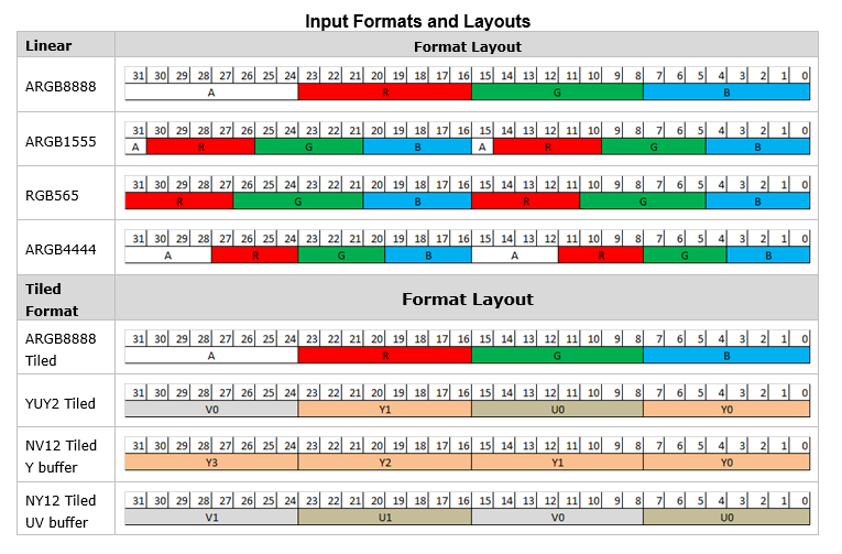
Data arrangement of linear input formats
Pixel data in linear format is stored in frame buffer memory, line by line, from left to right and from top to bottom.
Only the RGB format supports the linear mode. The linear burst size is fixed at 128 bytes.
Figure 426.
Pixel data arrangement - 64x1 linear mode

For the 32-bpp RGB format data, 128 bytes are stored in 32x1 linear mode.
Figure 427.
Pixel data arrangement - 32x1 linear mode

Data arrangement of ARGB8888 tiled and YUY2 tiled
The ARGB8888 and YUY2 tiled formats use a 4x4 tile. The data burst size is 64 bytes for both formats. For the ARGB8888 tiled format, one burst fetches one tile. For the YUY2 tiled format, one burst fetches two continuous tiles in the horizontal direction.
Figure 428.
Request burst size for ARGB8888 tiled format

Figure 429.
Request burst size for YUY2 tiled format

Note:
The horizontal tile number for one frame of the YUY2 tiled format must be an even number.
The pixel data arrangement inside the tile, and tile data arrangement among tiles, for the two formats are shown in the following figures.
Figure 430.
Pixel data arrangement inside the tile
Figure 431.
Tiled data arrangement among tiles
Data arrangement of NV12 tiled Y buffer and NV12 tiled UV
The NV12 tiled format uses an 8x8 tile for Y planar, and a 4x4 tile for UV planar. The burst size is 32 bytes for both the Y and UV data. For Y planar, one burst fetches half the Y tile (8x4). For UV planar, one burst fetches one UV tile.
One 8x8 tile for Y planar needs to be fetched by two bursts: one is the upper 8x4 part; the other is the lower 8x4 part, as shown in the following figure.
Figure 432.
Burst division of one 8x8 tile for Y planar
Figure 433.
Request burst size in one tile line for Y planar
The pixel data arrangement inside the tile and tile data arrangement among tiles for the two formats are shown in the following figures.
Figure 434.
Pixel data arrangement inside the tile for Y planar
Figure 435.
Pixel data arrangement inside the tile for UV planar
Figure 436.
Tile data arrangement among tiles for Y planar
Figure 437.
Tile data arrangement among tiles and request burst size for UV planar
Alignments and maximum read OTs
Different input formats may require varied AXI burst lengths. Stride and base addresses must be aligned to the burst length. The base address and stride for linear data must be 128-byte aligned.
The input format of a video/graphic or overlay layer also affects the maximum number of read outstanding transactions (OTs) for the layer. One layer supports 2K-byte requests before data is returned. The total number of read OTs for all the video/graphic and overlay layers cannot exceed 64.
The following table provides the alignments of stride and base address, and the maximum read OTs for one layer in different input formats.
Linear/Tiled | Input format | AXI burst length (Bytes) | Maximum read OTs per layer | Stride alignment (Bytes) | Base address alignment (Bytes) |
|---|---|---|---|---|---|
Linear | ARGB8888 | 128 | 16 | 128 | 128 |
ARGB1555 | 128 | 16 | 128 | 128 | |
RGB565 | 128 | 6 | 128 | 128 | |
ARGB4444 | 128 | 16 | 128 | 128 | |
Tiled | ARGB8888 Tiled | 64 (4 bytes x 16 pixels) | 32 | 128 | 128 |
YUY2 Tiled | 64 [2 bytes x (16+16) pixels] | 32 | 64 | 64 | |
NV12 Tiled | 32 | 64 | Y:64 UV:32 | Y:64 UV:32 |
Stride alignment examples
Stride alignment adds bytes to the end of each pixel line or tile line to ensure the data pattern meets the hardware request.
For linear format data, the stride is used to align each pixel line. If one frame in linear format is not aligned to 128 bytes in width, software pads dummy data after each pixel line to make it aligned to 128 bytes.
Figure 438.
Stride alignment example for frame in linear mode
For the tiled format data, the stride is used to align each tile line. If one frame in tiled format is not aligned to the requested stride in tile line, software pads dummy data after each tile line to align it to the requested value.
Figure 439.
Stride alignment for frame in tiled mode
Output formats
The display controller can use either the MIPI display pixel interface (DPI) or display bus interface (DBI) for output. Both the DPI and DBI support RGB formats as listed in the following table. Note that the DPI interface is not available on PSOC™ Edge GPIOs. It is only an internal connection to the MIPI DSI controller.
Interface | Output format |
|---|---|
DPI |
|
DBI Type A and DBI Type B |
|
DBI Type C | RGB565 and RGB888
|
DBI interface
The display bus interface (DBI) is the default interface. The display controller can output either DBI Type A Fixed E, Type A Clocked E, Type B, or Type C. All these DBI types support RGB formats.
The following table describes the signals applicable to different DBI types and provides signal mapping between MIPI DBI specifications and the display controller.
Signal | DC DBI Signal | Width | I/O | Description |
|---|---|---|---|---|
CSX | dbiTypeab_csx | 1 | OUT | Chip Select for DBI Type A or B. Display module is selected when low. It is tied to 0 for DBI Type A in Clocked E mode. |
dbiTypecCsx | 1 | OUT | Chip Select for DBI Type C. Display module is selected when low. | |
D15:0 | dbiTypeab_data | 8 | OUT | Information signal for DBI Type A or B |
D/CX | dbiTypeab_dcx | 1 | OUT | Data/Command indicator for DBI Type A or B Command is active when low. |
dbiTypecDcx | 1 | OUT | Data/Command indicator for DBI Type C option 3. Command is active when low. | |
R/WX for Type A RDX for Type B | dbiTypeab_rwx_or_rdx | 1 | OUT | For DBI Type A, specifies whether the current cycle is for read (1) or write (0) and tied to 0. For DBI Type B, specifies whether the current cycle is for read (0) or write (1) and tied to 1. For DBI Type A and Type B, read is not supported. |
WRX | dbiTypeab_wrx | 1 | OUT | Write signal for DBI Type B. Host processor writes data at falling edge. |
E | dbiTypeaE | 1 | OUT | E clock for DBI Type A. It is tied to 1 for DBI Type A in Fixed E mode. |
/ | sdaClk | 1 | IN | Input clock for DBI Type C, used to generate the dbiTypecScl signal. (not a standard signal defined for MIPI DBI) |
SCL | dbiTypecScl | 1 | OUT | Serial clock for DBI Type C. Host processor writes information or reads information at rising edge. It is tied to 0 if unused. |
DOUT | dbiTypecSdo | 1 | OUT | Information signal output for DBI Type C. For DBI Type C, read is not supported. |
/ | dbiTypecSdoEn | 1 | OUT | Output enable signal for dbiTypecSdo (not a standard signal defined for MIPI DBI) |
Note:
The RESX, TE, DIN, and SDA signals are not supported in the DC8000Nano design.
DBI type A and type B format setting
The DBI Type A and Type B support multiple RGB formats as listed in the following table.
To enable DBI output, set the register field gcregDbiConfig.BUS_OUTPUT_SEL = 1.
The register field gcregDbiConfig.DBI_DATA_FORMAT serves to set an output format for DBI Type A and Type B, whose values include:
0: (Default) Represents D8R3G3B2, an RGB332 format
1: Represents D8R4G4B4, an RGB444 format
2: Represents D8R5G6B5, an RGB565 format
3: Represents D8R6G6B6, an RGB666 format
4: Represents D8R8G8B8, an RGB888 format
5: Represents D9R6G6B6, an RGB666 format
6: Represents D16R3G3B2, an RGB332 format
7: Represents D16R4G4B4, an RGB444 format
8: Represents D16R5G6B5, an RGB565 format
9: Represents D16_R6_G6_B6_OP1, an RGB666 format
A: Represents D16_R6_G6_B6_OP2, an RGB666 format
B: Represents D16_R8_G8_B8_OP1, an RGB888 format
C: Represents D16_R8_G8_B8_OP2, an RGB888 format
Figure 440.
RGB formats for DBI Type A and Type B output
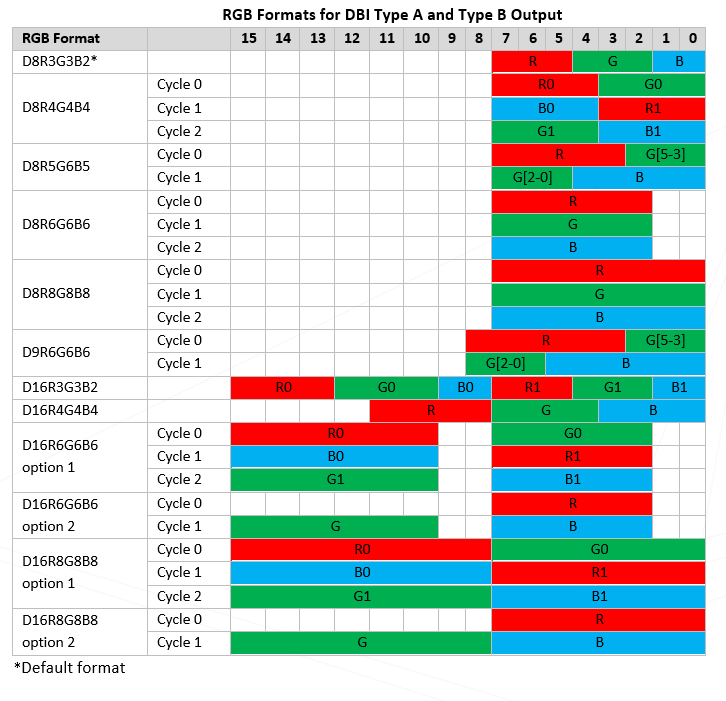
DBI type C format setting
The DBI Type C supports three output options for every 8-bit RGB data: option 1 for 9-bit output, option 2 for 16-bit output, and option 3 for 8-bit output.
The following three tables list the output cycles for RGB formats of the three DBI Type C options, respectively.
To enable DBI output, set the register field gcregDbiConfig.BUS_OUTPUT_SEL = 1.
The register field gcregDbiConfig.DBI_DATA_FORMAT serves to set an output format for DBI Type C, whose values include:
D: Represents D1R5G6B5, an RGB565 format
E: Represents D1R8G8B8, an RGB888 format
The register field gcregDbiConfig.DBI_TYPEC_OPT serves to set a DBI Type C output option for every 8-bit RGB data, whose values are:
0:Represents option 1
Figure 441. 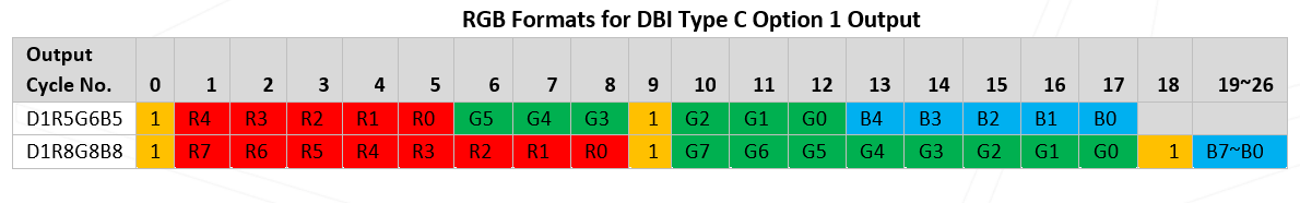
1: Represents option 2
Figure 442. 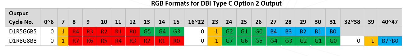
2: Represents option 3
Figure 443. 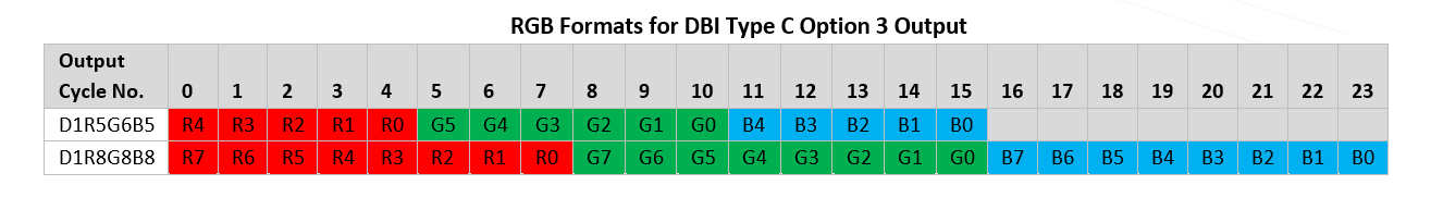
Note:
The value 1 in the orange box is an indicator bit for data transmission.
The method of programming DBI timing varies with the DBI type. The DBI Timing Configuration Register Fields table lists the timing registers used to set AC information (such as when to assert/de-assert a signal) for each DBI type. The Display Controller uses t
unit
to drive control and data signals and calculate the write period time, which defines:
Time unit of the ACLK cycle number for DBI Type A and Type B
Time unit of the sdaClk cycle number for DBI Type C
t
unit
=gcregDbiConfig.AC_TIME_UNIT+1 and the minimum value of the register field is 0.
MIPI DBI has defined different AC characteristics for each DBI type and the timing register configuration must follow corresponding AC characteristics. The following sections describe the output timing configuration and constraints for each DBI type.
Timing Register Field | DBI Type A Fixed E Mode | DBI Type A Clocked E Mode | DBI Type B | DBI Type C |
|---|---|---|---|---|
gcregDbiConfig.AC_TIME_UNIT | Time unit factor of the ACLK cycle number | Time unit factor of the ACLK cycle number | Time unit factor of the ACLK cycle number | Time unit factor of the sdaClk cycle number |
gcregDbiWrChar1.DBI_WR_CS_ASSERT | CSX assert timing | |||
gcregDbiWrChar1.DBI_WR_EOR_WR_ASSERT | D15:0 assert timing | E and D15:0 assert timing | WRX and D15:0 assert timing | |
gcregDbiWrChar1.DBI_WR_PERIOD | Total ACLK cycle number in a single write period = Register field value x t unit | |||
gcregDbiWrChar2.DBI_WR_EOR_WR_DE_ASRT | E de-assert timing | WRX de-assert timing | ||
gcregDbiWrChar2.DBI_WR_CS_DE_ASRT | CSX de-assert timing | |||
gcregDbiTypecCfg.TAS | SCL and DOUT assert timing | |||
gcregDbiTypecCfg.SCL_TWRL | sdaClk cycles during which SCL stays low in a single write period = Register field value x t unit | |||
gcregDbiTypecCfg.SCL_TWRH | sdaClk cycles during which SCL stays high in a single write period = Register field value x t unit | |||
Figure 444.
Output Timing Definition for DBI Type A Fixed E Mode
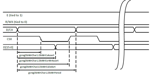
Figure 445.
Output Timing Definition for DBI Type A Clocked E Mode
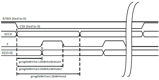
The following table describes the timing registers used for DBI Type A (see
Figure 444
and
Figure 445
).
DBI Type A Timing Register Field | Description for Fixed E Mode | Description for Clocked E Mode |
|---|---|---|
gcregDbiWrChar1.DBI_WR_CS_ASSERT | CSX assert timing | |
gcregDbiWrChar1.DBI_WR_EOR_WR_ASSERT | D15:0 assert timing | E and D15:0 assert timing |
gcregDbiWrChar2.DBI_WR_EOR_WR_DE_ASRT | E de-assert timing | |
gcregDbiWrChar2.DBI_WR_CS_DE_ASRT | CSX de-assert timing | |
gcregDbiWrChar1.DBI_WR_PERIOD | Single write period duration |
The assert and de-assert register fields, together with t unit , decide the ACLK cycle duration after which the corresponding signals are asserted or de-asserted.
n For Fixed E mode:
If gcregDbiWrChar1.DBI_WR_CS_ASSERT = 4, ACLK cycle number =4x t unit . This means the CSX signal is asserted after (4x t unit ) ACLK cycles.
n For Clocked E mode:
If gcregDbiWrChar1.DBI_WR_EOR_WR_ ASSERT = 4, ACLK cycle number = 4x t unit . This means the E or D15:0 signal is asserted after (4x t unit ) ACLK cycles.
gcregDbiWrChar1.DBI_WR_PERIOD decides the total ACLK cycle number in a single write period.
Total ACLK cycle numbers in a single write period = gcregDbiWrChar1.DBI_WR_PERIOD x t unit
The display controller includes a write period counter to manage signal driving. This register field configures the maximum value of this counter.
The write period counter starts from 0 for each signal. When it increments to the assert or de-assert timing configured by the assert or de-assert timing register fields, the corresponding signal is asserted or de-asserted.
DBI Type A Output Timing Constraints
The following figures show the AC characteristics of DBI Type A defined in MIPI DBI.
Figure 446.
AC characteristics of DBI Type A Fixed E Mode
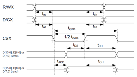
Figure 447.
AC characteristics of DBI Type A Clocked E Mode
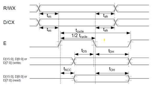
Figure 448.
AC characteristics description of DBI Type A
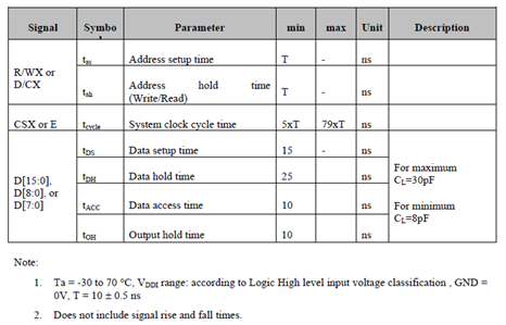
The timing register configuration for DBI Type A must meet the following requirements to ensure that its output timing follows the defined AC characteristics:
For Fixed E mode:
gcregDbiWrChar1.DBI_WR_CS_ASSERT >= 1
The time when the CSX signal is asserted is calculated using the following formula:
gcregDBIWrChar1.DBI_WR_CS_ASSERT x t unit x Single ACLK cycle duration
As required by AC characteristics for DBI Type A Fixed E mode in
Figure 446
and
Figure 448
, CSX should be asserted after one t
as
. One t
as
lasts one T with 10 ns as the time unit for T.
Therefore, the calculated CSX assert timing must be greater than or equal to 10 ns.
gcregDbiWrChar1.DBI_WR_CS_ASSERT < gcregDbiWrChar2.DBI_WR_CS_DE_ASRT < gcregDbiWrChar1.DBI_WR_PERIOD
gcregDbiWrChar1.DBI_WR_PERIOD >= 3
If the value of gcregDbiWrChar1.DBI_WR_PERIOD is less than 3, the display controller always changes it to 3.
For Clocked E mode:
gcregDbiWrChar1.DBI_WR_EOR_WR_ASSERT >= 1
The time when the E signal is asserted is calculated using the following formula:
grecgDbiWrChar1.DBI_WR_EOR_WR_ASSERT x t
unit
x Single ACLK Cycle duration
As required by AC characteristics for DBI Type A Clocked E mode in
Figure 447
and
Figure 448
, E should be asserted after one t
as
. One t
as
lasts one T with 10 ns as the time unit for T.
Therefore, the calculated E assert timing must be greater than or equal to 10 ns.
gcregDbiWrChar1.DBI_WR_EOR_WR_ASSERT < gcregDbiWrChar2.DBI_WR_EOR_WR_DE_ASRT < gcregDbiWrChar1.DBI_WR_PERIOD
gcregDbiWrChar1.DBI_WR_PERIOD >= 3
If the value of gcregDbiWrChar1.DBI_WR_PERIOD is less than 3, the display controller always changes it to 3.
Figure 449.
Output Timing Definition for DBI Type B
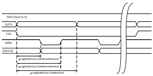
DBI Type B Timing Register Field | Description for DBI Type B |
|---|---|
gcregDbiWrChar1.DBI_WR_EOR_WR_ASSERT | WRX and D15:0 assert timing |
gcregDbiWrChar2.DBI_WR_EOR_WR_DE_ASRT | WRX de-assert timing |
gcregDbiWrChar1.DBI_WR_PERIOD | Single write period duration |
The assert and de-assert register fields together with t unit decide the ACLK cycle duration after which the corresponding signals are asserted or de-asserted.
If gcregDbiWrChar1.DBI_WR_EOR_WR_ASSERT = 4, the WRX or D15:0 signal is asserted after (4xt unit ) ACLK cycles.
gcregDbiWrChar1.DBI_WR_PERIOD decides the ACLK cycle number in a single write period.
Total ACLK cycle number in a single write period = gcregDbiWrChar1.DBI_WR_PERIOD x t unit
The display controller includes a write period counter to manage signal driving. This register field configures the maximum value of this counter.
The write period counter starts from 0 for each signal. When it increments to the assert or de-assert timing configured by the assert or de-assert timing register fields, the corresponding signal is asserted or de-asserted.
The following figures show the AC characteristics of DBI Type B defined in MIPI DBI.
Figure 450.
AC characteristics of DBI Type B
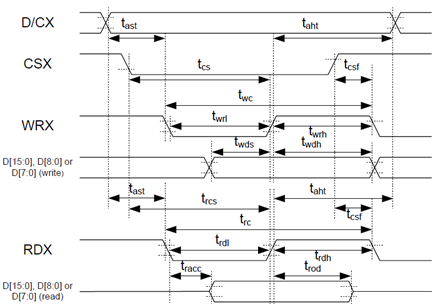
Figure 451.
AC characteristics description of DBI Type B
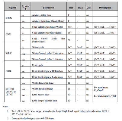
The timing register configuration for DBI Type B must meet the following requirements to ensure that its output timing follows the defined AC characteristics:
gcregDbiWrChar1.DBI_WR_EOR_WR_ASSERT >= 1
The time when the WRX signal is asserted is calculated using the following formula:
gcregDbiWrChar1.DBI_WR_EOR_WR_ASSERT x t unit x Single ACLK cycle duration
As required by AC characteristics for DBI Type B in Figure 9 and Figure 10, WRX should be asserted after one t
ast
. One t
ast
lasts one T with 10 ns as the time unit for T.
Therefore, the calculated WRX assert timing must be greater than or equal to 10 ns.
gcregDbiWrChar1.DBI_WR_EOR_WR_ASSERT < gcregDbiWrChar2.DBI_WR_EOR_DE_ASRT < gcregDbiWrChar1.DBI_WR_PERIOD
gcregDbiWrChar1.DBI_WR_PERIOD >= 3
If the value of gcregDbiWrChar1.DBI_WR_PERIOD is less than 3, the display controller always changes it to
DBI Type C Output Timing Configuration
Figure 452.
Output timing definition for DBI Type C
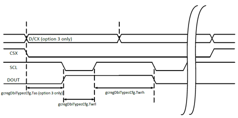
The following table describes the timing registers used for DBI Type C.
DBI Timing Register Field | Description for DBI Type C |
|---|---|
gcregDbiTypecCfg.TAS | SCL and DOUT assert timing |
gcregDbiTypecCfg.SCL_TWRL | sdaClk cycles during which SCL stays low in a single write period = Register field value x t unit |
gcregDbiTypecCfg.SCL_TWRH | sdaClk cycles during which SCL stays high a single write period = Register field value x t unit |
These timing registers, together with t unit , decide the sdaClk cycle duration after which the corresponding signals are asserted or de-asserted.
gcregDbiTypecCfg.TAS together with t unit decides the sdaClk cycle duration after which the SCL or DOUT signal is asserted.
The sum of gcregDbiTypecCfg.SCL_TWRL and gcregDbiTypecCfg.SCL_TWRH decides the total sdaClk cycle number in a single write period.
Total sdaClk cycle number in a single write period = (gcregDbiTypecCfg.SCL_TWRL + gcregDbiTypecCfg.SCL_TWRH) x t unit
The display controller includes a write period counter to manage signal driving. The sum result decides the maximum value of this counter.
The write period counter starts from 0 for each signal. When it increments to the assert timing configured by the assert timing register field, the corresponding signal is asserted.
DBI Type C Output Timing Constraints
The following figures show the AC characteristics of DBI Type C defined in MIPI DBI.
Figure 453.
AC characteristics of DBI Type C
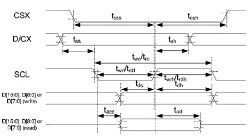
Figure 454.
AC characteristics description of DBI Type C
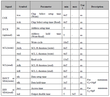
The timing register configuration for DBI Type C must meet the following requirements to ensure that its output timing follows the defined AC characteristics:
gcregDbiTypecCfg.SCL_TAS >= 1
The time when the SCL signal is asserted is calculated using the following formula:
gcregDbiTypeCfg.SCL_TAS x t unit x Single sdaClk cycle duration
As required by AC characteristics for DBI Type C in Figure 12 and Figure 13, SCL should be asserted after T when D/CX is asserted. One t
as
lasts one T with 10 ns as the time unit for T.
Therefore, the calculated SCL assert timing must be greater than or equal to 10 ns.
gcregDbiTypecCfg.SCL_TWRL >= 1 and gcregDbiTypecCfg.SCL_TWRH >= 1
As required by AC characteristics for DBI Type C in Figure 13, SCL must stay high or low for more than 4T. 10 ns is the time unit for T. SCL high or low duration must be greater than or equal to 40 ns.
Single write period duration is calculated as follows:
(gregDbiTypecCfg.SCL
TWRL
= gcregDbiTypeCfg.SCL
TWRH
) x t
unit
x Single sdaClk cycle duration
DBI frame transfer action flows
The following sections provide the basic steps to set the display output and frame data for DBI mode transfer for:
Initialization
Refresh of panel frame buffer
Partial refresh of panel frame buffer
The display controller design assumes that, for a display module with DBI, a display controller software driver provides the command file for initializing the control registers in the display module.
Initialization
Initialization should be done after the display is powered on. The following figure shows the DBI initialization timing.
Figure 455.
DBI Initialization timing
Set gcregPanelConfig.CLOCK=0 (DISABLED). This setting is mandatory for DBI mode. In DBI mode, the display controller ignores the values of any other bits in the gcregPanelConfig register
Set the DBI type for output. gcregDbiConfig.DBI_TYPE=Type A Fixed E, Type A Clocked E, or Type B, or Type C. For DBI Type C, you must also set the option; gcregDbiConfig.DBI_TYPEC_OPT = Option 1, Option 2, or Option 3.
Set the DBI bus in idle state. gcregDbiIfReset.DBI_IF_LEVEL_RESET=1[RESET]
Set the DBI output timing parameters and the AC timing specifications of the panel.
Registers for DBI Type A or Type B:
gcregDbiWrChar1
gcregDbiWrChar2
Register for DBI Type C:
gcregDbiTypecCfg
Set the output bus mode to DBI. gcregDbiConfig.BUS_OUTPUT_SEL=1
Write the gcregDbiCmd register to send configuration data. Commands must be entered one by one.
gcregDbiCmd.DBI_COMMANDFLAG=00 indicates an address is to be written. The address to be sent to the DBI port is stored in gcregDbiCmd.DBI_COMMAND_WORD
gcregDbiCmd.DBI_COMMANDFLAG=10 indicates writing one parameter to the display. The parameter is stored in gcregDbiCmd.DBI_COMMAND_WORD
Refresh of panel frame buffer (single frame example)
Set timing parameters according to the actual panel specifications
Parameters are set before the first frame refresh, and then are ignored after that.
gcregHDisplay.TOTAL = gregHDisplay.DISPLAY_END = panel width size
gcregHSync.START = 0
gcregHSync.END = panel width
gcregVDisplay.TOTAL = panel height + 1
The extra value
1
is used for waiting for the data FIFO to be filled. This extra value should be 2 for the tile data format.
gcregVDisplay.DISPLAY_END = panel height
gcregVSync.START=0
gcregVSync.END = panel height
Set the registers for the cursor, gamma, or dither function (if required)
gcregCursor*
gcregGamma*
gcregDisplayDither*
gcregPanelFunction.GAMMA
gcregPanelFunction.Dither
Set the frame buffer address or overlay address, stride, layer size, and location
gcregFrameBufferAddress
gcregOverlayAddress
gcregOverlayAddress1
gcregFrameBufferStride
gcregOverlayStride
gcregOverlayStride1
gcregDcTileUvFrameBufferAdr
gcregDcTileUvFrameBufferStr
gcregDcTileUvOverlayAdr
gcregDcTileUvOverlayStr
gcregVideoTL
gcregFrameBufferSize
gcregOverlayTL
gcregOverlaySize
gcregOverlayTL1
gcregOverlaySize1
For tiled formats, any of the following stride register values = one-line stride x tile height:
gcregFrameBufferStride
gcregOverlayStride
gcregOverlayStride1
gcregDcTileUvFrameBufferStr
gcregDcTileUvOverlayStr
Configure the data format of the frame buffer and enable the layer
gcregPanelFunction.OUTPUT=1 indicates the output panel is enabled.
gcregFrameBufferConfig.Enable=1 indicates the video/graphic layer is enabled.
gcregOverlayConfig.Enable=1 indicates overlay layer 0 is enabled.
gcregOverlayConfig1.Enable=1 indicates overlay layer 1 is enabled.
Registers used to indicate tiled ARGB8888, YUY2, and NV12 formats:
gcregDcTileIncfg
gcregDcOverlayTileIncfg
When the linear ARGB8888, ARGB1555, RGB565, or ARGB4444 format is expected, the tiled format fields of these registers must be set to none.
Registers used to indicate the linear ARGB8888, ARGB1555, RGB565, and ARGB4444 formats:
gcregFrameBufferConfig.Format
gcregOverlayConfig.Format
gcregOverlayConfig1.Format
Write the gcregDbiCmd register to send configuration data. Commands are entered one by one.
gcregDbiCmd.DBI_COMMAND.FLAG=1[WRITE_MEM_START] indicates writing to the DBI bus. For this flag setting, the value of gcregDbiCmd.DBI_COMMAND_WORD is ignored.
Use the interrupt registers to wait for the signal of which the write is completed, or check the interrupt status.
gcregDisplayIntr
gcregDisplayIntrEnable
Repeat the preceding steps for each succeeding frame as needed
Partial refresh of panel frame buffer (single frame example)
Set timing parameters according to the actual panel specifications.
Parameters are set before the first frame refresh, and then ignored after that.
gcregHDisplay.TOTAL = gregHDisplay.DISPLAY_END = partial window width size
gcregHSync.START = actual clipped window x start
gcregHSync.END = actual clipped window x end
gcregVDisplay.TOTAL = partial window height + 1
ixia_locid="1102">The extra value 1 is used for waiting for the data FIFO to be filled. This extra value should be 2 for tile data format.
gcregVDisplay.DISPLAY_END = partial window height
gcregVSync does not require setting for the linear format.
For tiled data: gcregVSync.START = actual clipped window y start
gcregVSync.END = actual clipped window y end
Set the registers for the cursor, gamma, or dither function (if required).
gcregCursor*
gcregGamma*
gcregDisplayDither*
gcregPanelFunction.GAMMA
gcregPanelFunction.Dither
Set the frame buffer address, overlay address, stride, layer size, and location
gcregFrameBufferAddress
gcregOverlayAddress
gcregOverlayAddress1
gcregFrameBufferStride
gcregOverlayStride
gcregOverlayStride1
gcregDcTileUvFrameBufferAdr
gcregDcTileUvFrameBufferStr
gcregDcTileUvOverlayAdr
gcregDcTileUvOverlayStr
gcregVideoTL
gcregFrameBufferSize
gcregOverlayTL
gcregOverlaySize
gcregOverlayTL1
gcregOverlaySize1
For tiled formats, any of the following stride register values = one-line stride x tile height:
gcregFrameBufferStride
gcregOverlayStride
gcregOverlayStride1
gcregDcTileUvFrameBufferStr
gcregDcTileUvOverlayStr
Configure the data format of the frame buffer and enable the layer
gcregPanelFunction.OUTPUT=1 indicates output panel is enabled.
gcregFrameBufferConfig.Enable=1 indicates the video/graphic layer is enabled.
gcregOverlayConfig.Enable=1 indicates overlay layer 0 is enabled.
gcregOverlayConfig1.Enable=1 indicates overlay layer 1 is enabled.
Registers used to indicate the tiled ARGB8888, YUY2, and NV12 formats:
gcregDcTileIncfg
gcregDcOverlayTileIncfg
When the linear ARGB8888, ARGB1555, RGB565, or ARGB4444 format is expected, the tiled format fields of these registers must be set to none.
Registers used to indicate the linear ARGB8888, ARGB1555, RGB565, and ARGB4444 formats: gcregFrameBufferConfig.Format
gcregOverlayConfig.Format
gcregOverlayConfig1.Format
Write the gcregDbiCmd register to send configuration data for the partial window. Commands are entered one by one
gcregDbiCmd.DBI_COMMANDFLAG=1[WRITE_MEM_START] indicates writing to the DBI bus.
For this flag setting, the value of gcregDbiCmd.DBI_COMMAND_WORD is ignored.
Use the interrupt registers to wait for the signal that the write is completed, or check the interrupt status
gcregDisplayIntr
gcregDisplayIntrEnable
Repeat the preceding steps for each succeeding frame as needed
DPI interface
When the display controller uses the display pixel interface (DPI) as the output interface, the DPI supports RGB formats in 24-bit data signals.
Note:
The DPI interface is not available on PSOC™ Edge GPIOs. It is only an internal connection to the MIPI DSI controller.
The following table lists the signals applicable to DPI. They reside in the pixel clock domain.
Signal | Width | I/O | Description |
|---|---|---|---|
displayColor | 24 | OUT | Display color |
displayClk | 1 | OUT | Display pixel clock |
displayEn | 1 | OUT | Display enable |
displayHsync | 1 | OUT | Display horizontal synchronization |
displayVsync | 1 | OUT | Display vertical synchronization |
dispReady | 1 | IN | Display ready |
pixelClk | 1 | IN | Display clock |
DPI output format setting
The DPI interface supports multiple RGB formats as listed in the following table.
To enable DPI output, set the register field gcregDbiConfig.BUS_OUTPUT_SEL = 0.
The register field gcregDpiConfig.DPI_DATA_FORMAT serves to set a DPI output format, whose values are:
0: Represents D16CFG1, an RGB565 format
1: Represents D16CFG2, an RGB565 format
2: Represents D16CFG3, an RGB565 format
3: Represents D18CFG1, an RGB666 format
4: Represents D18CFG2, an RGB666 format
5: (Default) Represents D24, an RGB888 format
Figure 456.
RGB formats for DPI output
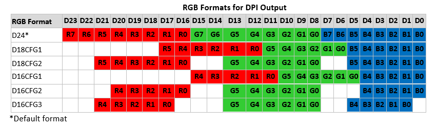
DPI output timing
The following figure shows the timing diagram for the display Hsync and displayVsyn signals and the associated configuration registers.
The display Hsync related timing parameters are
H Sync pulse
,
H Front porch
, and
H Back porch
as shown in the following figure. The associated timing register settings are as follows:
gcregHSync.Start = gcregHDisplay.DisplayEnd + H Front porch
gcregHSync.End = gcregHSync.Start + H Sync pulse
gcregHDisplay.Total = gcregHSync.End + H Back porch
The displayVsync related timing parameters are
V Sync pulse
,
V Front porch
, and
V Back porch
as shown in the following figure. The associated timing register settings are as follows:
gcregVSync.Start = gcregVDisplay.DisplayEnd + V Front porch
gcregVSync.End = gcregVSync.Start + V Sync pulse
gcregVDisplay.Total = gcregVSync.End + V Back porch
For more details about these registers, see the Registers documentation.
When the DPI mode starts working, output timing keeps working unless it is stopped manually. In this case, only double-buffered registers can be updated between frames.
Figure 457.
Timing diagram osf displayHsync and displayVsync
DPI timing configuration example
This section uses the display resolution, 640x480@60 Hz, as an example to describe the timing register setting. The following tables provide the industry-standard horizontal and vertical timing parameters for this display resolution.
Horizontal timing (line): Polarity of horizontal sync pulse is negative
Scanline part | Pixels |
|---|---|
Visible area | 640 |
Front porch | 16 |
Sync pulse | 96 |
Back porch | 48 |
Whole line | 800 |
According to the parameter values in the table above, if the visible area indicates the value of gcregHDisplay.DisplayEnd, then:
gcregHSync.Start = gcregHDisplay.DisplayEnd + H Front porch = 640 + 16 = 656
gcregHSync.End = gcregHSync.Start + H Sync pulse =656 + 96 = 752
gcregHDisplay.Total = gcregHSync.End + H Back porch = 752 + 48 = 800
Vertical timing (frame): Polarity of vertical sync pulse is negative.
Frame part | Lines |
|---|---|
Visible area | 480 |
Front porch | 10 |
Sync pulse | 2 |
Back porch | 33 |
Whole frame | 525 |
According to the parameter values in the table above, if the visible area indicates the value of gcregVDisplay.DisplayEnd, then:
gcregVSync.Start = gcregVDisplay.DisplayEnd + V Front porch = 480 + 10 = 490
gcregVSync.End = gcregVSync.Start + V Sync pulse = 490 + 2 = 492
gcregVDisplay.Total = gcregVSync.End + V Back porch = 492 +33 = 525
DPI frame
This section describes the basic steps to set the display output and frame data for DPI mode transfer. The register documentation includes additional detail on the registers referenced below.
Set the timing parameters according to the specifications for the target panel.
See Section: DPI Output Timing for the timing register configuration.
gcregHDisplay
gcregHSync
gcregVDisplay
gcregVSync
Set registers for the cursor, gamma, or dither function (if required)
gcregCursor*
gcregGamma*
gcregDisplayDither*
gcregPanelFunction.GAMMA
gcregPanelFunction.Dither
Set the frame buffer address, overlay address, stride, layer size, and location
gcregFrameBufferAddress
gcregOverlayAddress
gcregOverlayAddress1
gcregFrameBufferStride
gcregOverlayStride
gcregOverlayStride1
gcregDcTileUvFrameBufferAdr
gcregDcTileUvFrameBufferStr
gcregDcTileUvOverlayAdr
gcregDcTileUvOverlayStr
gcregVideoTL
gcregFrameBufferSize
gcregOverlayTL
gcregOverlaySize
gcregOverlayTL1
gcregOverlaySize1
For tiled formats, any of the following stride register values = one-line stride x tile height:
gcregFrameBufferStride
gcregOverlayStride
gcregOverlayStride1
gcregDcTileUvFrameBufferStr
gcregDcTileUvOverlayStr
Set the output bus mode to DPI
gcregDbiConfig.BUS_OUTPUT_SEL=0
Configure the panel and panel timing requirements
n gcregPanelConfig
Configure the data format of the frame buffer and enable the layer
gcregPanelFunction.OUTPUT=1 indicates output panel is enabled.
gcregFrameBufferConfig.Enable=1 indicates the video/graphic layer is enabled.
gcregOverlayConfig.Enable=1 indicates overlay layer 0 is enabled.
gcregOverlayConfig1.Enable=1 indicates overlay layer 1 is enabled.
Registers used to indicate the tiled ARGB8888, YUY2, and NV12 formats:
gcregDcTileIncfg
gcregDcOverlayTileIncfg
When the linear ARGB8888, ARGB1555, RGB565, or ARGB4444 format is expected, the tiled format field of these registers must be set to NONE.
Registers used to indicate the linear ARGB8888, ARGB1555, RGB565, and ARGB4444 formats:
gcregFrameBufferConfig.Format
gcregOverlayConfig.Format
gcregOverlayConfig1.Format
Start the interface mode transfer
gcregPanelWorking.WORKING=1
Update parameters for the next frame
gcregPanelControl.VALID=1 indicates the next frame configuration is completed.
Use the interrupt registers to wait for the signal of which the transfer is completed, or check the interrupt status
gcregDisplayIntr
gcregDisplayIntrEnable
Repeat the preceding steps for each succeeding frame as needed
Layer features
Hardware cursor
Cursor formats
The Display Controller supports both the ARGB8888 format and the mask format for the hardware cursor. The cursor size is 32x32.
In the ARGB8888 cursor format, the color of the cursor is decided by the ARGB values fetched from the memory.
In the masked cursor format, the mask values of the
AND
and
XOR
bits decide the color of one cursor pixel. The following table lists the color values for different bit configurations. The foreground and background colors are configured through the gcregCursorForeground and gcregCursorBackground registers, respectively.
Bit AND | Bit XOR | Color Value |
|---|---|---|
0 | 0 | Background color |
0 | 1 | Foreground color |
1 | 0 | Not used |
1 | 1 | Bit inversed foreground color |
Cursor position
The position of a cursor is tracked as follows:
The top-left point is used as the base address for the cursor
Hot spot is used in a search for a corresponding screen coordinate when a selection is made by pressing the "Enter" key or clicking the left mouse button
Figure 458.
Cursor Bounding Box

Figure 459.
Cursor hot spot

The position configured for a cursor through registers is the position of the hot spot in the display window.
Figure 460.
Cursor positions in a display window
Swizzle
One color format may be stored in different orders in the memory. To accommodate this possibility, the display controller can swizzle an input pixel at the video/graphic and overlay layers to switch the component position in the pixel data.
For RGB formats, the input pixel may be in any of the ARGB, RGBA, ABGR, and BGRA format orders. The display controller assumes the initial input of ARGB data is in ARGB order, which means A is in the upper bits while B is in the lowest bits. If the input is not in ARGB order, the display controller uses swizzle to reshape the data. For example, if the input format is in BGRA order, the swizzle must be configured to handle the BGRA format.
For YUV formats, especially for UV mixed formats, the U and V pixels may be placed in different positions. The display controller assumes that for each UV pair, U is in the lower bits while V is in the upper bits. If the input in not in this order, the display controller uses UV-swizzle to reshape the input data.
The following figure shows the expected input orders for the RGB format. If the input RGB data is not in these orders, swizzle is required.
Expected input organization for RGB format
32-bit formats
31
First Pixel=31:0
24
23
16
15
8
7
0
A8R8G8B8
A
A
A
A
A
A
A
A
R
R
R
R
R
R
R
R
G
G
G
G
G
G
G
G
B
B
B
B
B
B
B
B
16-bit Formats
31
First Pixel=15:0
Second Pixel=31:16
24
23
16
15
8
7
0
A1R5G5B5
A
R
R
R
R
R
G
G
G
G
G
B
B
B
B
B
A
R
R
R
R
R
G
G
G
G
G
B
B
B
B
B
A4R4G4B4
A
A
A
A
R
R
R
R
G
G
G
G
B
B
B
B
A
A
A
A
R
R
R
R
G
G
G
G
B
B
B
B
R5G6B5
R
R
R
R
R
G
G
G
G
G
G
B
B
B
B
B
R
R
R
R
R
G
G
G
G
G
G
B
B
B
B
B
Color space conversion
The display controller supports color space conversion of YUV2RGB for the video/graphic and overlay 0 layers. Either BT.601 YUV2RGB or BT.709 YUV2RGB can be used, which is configurable using the gcregDcTileInCfg and gcregDcOverlayTileInCfg registers.
In the YUV-to-RGB conversion, the display controller uses an 8-bit pipeline to convert the YUV data into an RGB format with 8 bits for each of the R, G, and B components.
Color keying
The Display Controller provides for overlay and transparency effects by using color keys at the video/graphic and overlay layers. Color keying enables the display controller to filter out a special color in a source image and replace it with another designated color of the destination image.
Color keying is usually performed before alpha blending and is supported only for the ARGB format.
Typical application scenarios include:
Display of an interesting scene behind people such as a weather map
Provision of special effects such as floating a car on the ocean
Color keying process
The Display Controller performs color keying on every two video/graphic layers and overlay layers, together with one background layer, in an ascending order. If any video/graphic or overlay layer is disabled, color keying is not applied to the disabled layer.
By default, overlay layer 1 has the highest order, overlay layer 0 the second, video/graphic layer the second lowest, and the background layer the lowest, as shown in the following figure. The stack order of the video/graphic and overlay layers is configurable.
The color of the background layer is configured using the gcregFrameBufferBackground register.
Figure 461.
Default lay order for color keying
When color keying is enabled and the default layer order is used, the display controller performs color keying on the paired layers in the following sequence:
Color keying for background and video/graphic layers:
The video/graphic layer is the source layer and the background layer is the destination layer. The Display Controller replaces the selected color of the video/graphic layer with the background color. The color-keyed video/graphic layer is then regarded as the destination layer for the color keying of overlay 0 and video/graphic layers.
Color keying for video/graphic and overlay 0 layers:
Overlay layer 0 is the source layer and the color-keyed video/graphic layer is the destination layer. The Display Controller replaces the selected special color of overlay layer 0 with the pixel color of the color-keyed video/graphic layer. The color-keyed overlay layer 0 is then regarded as the destination layer for the color keying of overlay 1 and overlay 0 layers.
Color keying for overlay 0 and overlay 1 layers:
Overlay layer 1 is the source layer and the color-keyed overlay layer 0 is the destination layer. The Display Controller replaces the selected special color of overlay layer 1 with the pixel color of the color-keyed overlay layer 0.
Color keying implementation
In a typical case, there is at least one source layer (foreground) and one destination layer (background), with the source layer displayed in front of the destination layer. The source layer contains a solid color (typically, blue or green).
The Display Controller performs color keying as follows:
Compare the component value of each pixel color of the source layer (R, G, B, or A of the color) with the color key range defined in the following registers, which are 32 bits of the ARGB8888 format:
gcregFrameBufferColorKey
gcregFrameBufferColorKeyHigh
gcregOverlayColorKey
gcregOverlayColorKeyHigh
gcregOverlayColorKey1
gcregOverlayColorKeyHigh1
Table 495.
Configuration for ColorKey and ColorKeyHigh Registers
Color Format
31
24
23
16
15
8
7
0
A8R8G8B8
A
A
A
A
A
A
A
A
R
R
R
R
R
R
R
R
G
G
G
G
G
G
G
G
B
B
B
B
B
B
B
B
When all of the components of the pixel color are in the range, the Display Controller regards it as a special color and filters it out
When the two layers are blended, the Display Controller uses the color of the destination layer to replace the special solid color in the source layer
The following figure shows an example of the blending result after color keying:
Figure 462.
Color Keying
RLAD
The Run-Length Adaptive Dithering (RLAD) decoder decodes compressed images on the fly. Using compressed images reduces the memory footprint for image storage.
The images must be encoded in one of the following formats:
Run-Length Adaptive Dithering (lossy format).
RLAD with uniform package size (less efficient, but can force a consistent read bandwidth if needed)
Run-Length Adaptive (lossless)
Standard Run-Length (lossless)
The RLAD format is a proprietary compression format optimized for low-complexity hardware decoding.
As an additional feature, the RLAD can be used for RGB packaging. It can read images stored in RGB888 or RGB666 format and provide it to the Display Controller (DC) in 32-bit frame buffer layout, resulting in a memory footprint reduction.
There is no hardware support for encoding imaging, hence it is required that encoding is done by software.
The following is the high-level block diagram of the RLAD.
Figure 463.
RLAD high-level block diagram
The RLAD block is fully transparent to the DC. The AXI read port is connected on the input side directly to the DC and on the output side to the AXI bridge. It handles all AXI read requests coming from the DC.
The decoding can be enabled for one specific layer. Only the selected layer is then automatically routed via the RLAD decoder block. All other layers are bypassing the RLAD decoder block. The layers are identified by their AXI read address ID provided by the DC.
The AXI read transactions must use the following configuration:
ARLEN[3:0] = 4’b1111 (16 beats per burst)
ARSIZE2:0 = 3’b011 (8bytes per beat)
ARBURST[1:0] = 2’b01 (incremental burst)
Resulting in bursts of 128 bytes. If the configuration does not match the defined criteria, the RLAD module raises an interrupt and enters the fail state.
The following diagram depicts the details of the AXI routing for the read address and the read data channel.
Figure 464.
RLAD AXI routing
To enable the block register, RLAD_ENABLE must be set to 1. All registers inside the RLAD block are shadowed and taken over via a pulse on input pin shadow_load_i. The input shadow_load_i is expected to be driven by the DC. The DC also uses a shadow mechanism. First, all configuration settings for the next frame must be updated for the DC as well as for the RLAD block. As a last command, the GCREGPANELCONTROL_VALID flag inside the DC must be set. Once this flag is set and the active display frame buffer is completed, the update of the shadow registers occurs. This mechanism allows to synchronize the configuration of the RLAD block with operation of the DC.
The decoding of an image is started if the base address of the image is seen on the read address channel together with is selected layer (read address ID). The base address is defined via the RLAD_ADRESS register. The detection is done in the RLAD block. To indicate the start of a new image, a trigger pulse is applied on the signal rlad_start.
The RLAD block always provides the data in ARGB8888 format to the DC. Each AXI burst contains 128 bytes representing the data for 32 pixels.
If the decoding is started, the RLAD block generates AXI read requests. It always requests 128-byte bursts. If the size of the encoded image is not a multiple of 128, the RLAD block continues to read until it reaches the subsequent 128-byte boundary. The size of the encoded image in number of 32-bit words minus one is defined in the RLAD_SIZE register.
The AXI master also uses the same AXI burst configuration as expected from DC on the input side resulting in bursts of 128 bytes.
ARLEN[3:0] = 4’b1111 (16 beats per burst)
ARSIZE2:0 = 3’b011 (8bytes per beat)
ARBURST[1:0] = 2’b01 (incremental burst)
Note:
Although the AXI configuration for DC read and RLAD block is the same, it is expected that the number of AXI transfers from the memory to the RLAD block is significantly lower than the number of AXI transfers between DC and RLAD. This is because the memory footprint of the encoded image is significantly smaller than the memory footprint of the original image.
The RLAD block fills an adjacent FIFO, which can take up to two 128-byte bursts. This is done to avoid any back pressure on the AXI bus when receiving a burst. A new burst is requested by the RLAD block when the FIFO can take at least one full 128-byte burst.
The output of the FIFO contains a data bit width conversion from 64- to 32-bit. This is required as the RLAD decoding block works with 32-bit data words.
For handling even and odd number of 32-bit data words for one image, add one bit of information into the FIFO. This bit indicates if both 32-bit data words or only one 32-bit data word is valid in the actual 64-bit FIFO entry. This bit can only be zero in the last FIFO entry of an encoded image. As a result, the FIFO has a bit width of 65 bits.
The following registers are used to define the behavior of the RLAD.
RLAD_WIDTH: Width of the image in number of pixels minus one. The DC layer must be setup for the same width
RLAD_HEIGHT: Height of the image in number of lines minus one. The DC layer must be setup for the same height
RLAD_MODE: Encoding mode
RLAD_BITS_R: Max number of red channel bits (used for RLAD modes only)
RLAD_BITS_G: Max number of green channel bits (used for RLAD modes only)
RLAD_BITS_B: Max number of blue channel bits (used for RLAD modes only)
RLAD_BITS_A: Max number of alpha channel bits (used for RLAD modes only)
The values of these registers must fit to the settings of the encoded image.
The encoded image data must be stored in the memory in the following way:
Figure 465.
RLAD encoded data byte order

The output of the RLAD block (o_rlad_red[7:0], o_rlad_green[7:0], o_rlad_blue[7:0] and o_rlad_alpha[7:0]) depends on the used settings. Therefore, you must adapt the RLAD output format to the format expected by the DC. The DC also requires an ARGB8888 format using 32 bits per pixel. Hence 2 pixels are provided per AXI beat. The following format is used:
Figure 466.
AXI data output format
The color format conversion and the combination of two 32-bit words to one 64-bit word is done in the RLAD colconv block. If the RLAD core can provide 1 pixel per clock cycle, new data can be provided on the AXI read data port every second clock cycle. The expected pixel rate on the RLAD output is approximately 8/9 pixels per clock.
The color conversion is defined via the RLAD_FORMAT and the RLAD_MODE registers .
Encoding mode (RLAD_MODE)
The following input encoding mode are available.
RLAD_MODE | Encoding mode |
|---|---|
0 | RLAD - Run-Length Adaptive Dithering (lossy). |
1 | RLAD_UNIFORM - RLAD with uniform package size (less efficient, but can force a consistent read bandwidth if needed). |
2 | RLA - Run-Length Adaptive (lossless). |
3 | RL - Standard Run-Length (lossless). |
Supported encoding modes
The configuration of the RLAD inputs a_width_wd, r_width_wd, g_width_wd, and b_width_wd are handled in the color conversion block and depend on the settings of the RLAD_MODE and RLAD_FORMAT registers. In all non RL modes, the values are directly derived out of the number of bits per pixel defined in the corresponding RLAD_FORMAT setting. For RL mode, the whole pixel is encoded at once which requires an additional encoding step.
The inputs a_width_wd, r_width_wd, g_width_wd and b_width_wd must be set based on the following scheme:
Bit per pixel | r_width_wd | g_width_wd | b_width_wd | a_width_wd |
|---|---|---|---|---|
4 | 0 | 0 | 0 | 4 |
6 | 0 | 0 | 0 | 6 |
8 | 0 | 0 | 0 | 8 |
12 | 0 | 0 | 4 | 8 |
16 | 0 | 0 | 8 | 8 |
18 | 0 | 2 | 8 | 8 |
24 | 0 | 8 | 8 | 8 |
32 | 8 | 8 | 8 | 8 |
RLAD configuration based on bits per pixel
The data coming out of the RLAD must also be rearranged. The data is not split per pixel anymore, and is represented as a whole pixel word instead. It has to be taken from that pixel word at the bit position that corresponds to the encoded color format.
Example for RGB565
pixel_word31:0 = [o_rlad_red[7:0], o_rlad_green[7:0], o_rlad_blue[7:0], o_rlad_alpha[7:0]]
red = pixel_word[15:11]
green = pixel_word[10:6]
blue = pixel_word5:0
alpha = 255
This step is done before the upscaling is applied.
The color format RGB444 is an exception. It has a different mapping which shown below.
red = pixel_word[7:4]
green = pixel_word[3:0]
blue = pixel_word[11:8]
alpha = 255
Color formats (RLAD_FORMAT)
The following input color formats options are available.
RLAD_FORMAT | Color format |
|---|---|
1 | ARGB4444 |
2 | ARGB1555 |
3 | RGB565 |
4 | ARGB8888 |
5 | RGB888 |
6 | RGB666 |
7 | RGB444 |
8 | GRAY8 |
9 | GRAY6 |
10 | GRAY4 |
Supported color formats
The output format is always an ARGB8888 format. For GRAY formats, the green channel is used for decoding the gray value from the RLAD core. The green channel is then replicated on the red and green channel and the alpha value is set to 0xFF to achieve a proper ARGB8888 format.
If the input format has less then 8 pixels, an upscaling must be done. This is done by using the following equation.
val_out = round(val_in * 255 / (2^bpc_in - 1))
To minimize the calculation effort, the following approximation is used.
val_out[i] = val_in[bpc_in - 1 - (bpc_out - i) % bpc_in], with i = 0 .. bpc_out – 1
The following drawing shows the algorithm for an input bit width of 3:
Figure 467.
Format conversion example
Line stride padding
The number of bytes per line must be a multiple of the burst length of 128 bytes. This alignment restriction of the Display Controller (DC) is handled by the RLAD rdata block by inserting padding data (value: 0x000000) at the end of the line in case the end of line is reached before the actual burst is finished. The pixel data of the next line starts then with the beginning of the next burst. The configuration of the line length is done via register RLAD_WIDTH.
Outstanding read requests
The RLAD rdata block collects a maximum number of eight outstanding read requests. As the addresses are assumed to be continuously ascending, it is not required to store the address value. To detect the error condition of a wrongly received start address (RLAD_ADDRESS), the information regarding if the address matches the start address or not is stored in a single-bit FIFO.
Error handling
The purpose of the error detection is to identify forbidden configurations and states within the RLAD blocks. Error conditions are flagged via the Display Controller (DC) interrupt. There is a general interrupt status flag INTR.RLAD_ERROR to indicate that the RLAD decode has entered its fail state. More detailed information about the root cause of the RLAD fail state is in register RLAD_STATUS.RLAD_FAILED. If there is more than one error condition, the first error condition is the one which is stored. If two or more error conditions occur exactly within the same clock cycle, prioritization is done based on the RLAD_FAILED value. The lower the number the higher the priority.
The following error conditions trigger the transition into the fail state.
RLAD_FAILED | Name | Description |
|---|---|---|
0 | OFF | No fail state (normal operation) |
1 | AXI_ERROR | An AXI error response was received when reading compressed image data. |
2 | BUF_TOO_SMALL | The RLAD_SIZE setting is inconsistent with the compressed image data (image decompression not complete when end of buffer was reached). |
3 | BUF_TOO_LARGE | The RLAD_SIZE setting is inconsistent with the compressed image data (image decompression completed before end of buffer was reached). |
4 | DC_INVALID_SIZE | The DC was reading the first pixel of a frame when it was not expected. This means an inconsistent setup of RLAD and DC configuration. |
5 | DC_INVALID_FORMAT | The DC was reading data with an unexpected burst length. This means an invalid buffer format was configured. |
RLAD fail states
If an error condition occurs, the decoding process is stopped, and the RLAD returns null data to the Display Controller (DC) whenever new data is requested. No more read accesses (AXI read address transfers) are requested anymore by the RLAD MST block. The pending data is still accepted by the master to avoid back pressure on the AXI interconnect. The RLAD interrupt is generated once all pending read transactions are completed by the AXI master. The arbitration for the layers not using RLAD encoding is still working.
The read data unit RLAD RDATA block still provides data to read requests from the DC but only provides null data. The read response always provides OKAY (slv_rresp_o = 2’b00).
To not influence non RLAD related image data reads in fail state, the AXI switch also works in RLAD fail state.
To leave the fail state, it is required to disable the RLAD block by setting RLAD.RLAD_ENABLE=0 and restart the RLAD block again. As all RLAD registers are shadowed, it is required that the DC generates the required update pulses for the loading the shadow register.
Synchronization
The output signal stat_rlad_failed_o representing the content of register RLAD_FAILED and the output signal interrupt_rlad_error_o for setting the RLAD interrupt are synchronized to clock clk_ahb_i.
All other signals are synchronous to clk_hf_core.
The configuration inputs cfg_rlad_XXX_i are assumed to be stable while they are taken over with the the pulse on input shadow_load_i.
Synchronous reset
Besides the asynchronous resets (rst_sys_n and rst_hf_n), the RLAD also supports a synchronous reset (sw_reset_hf_i). It is used to reset the whole RLAD synchronously. Within the Display Controller (DC) wrapper, this is done whenever the CTL.ENABLED register bit is set to 0. The synchronous reset is assumed to be synchronous to clk_hf. The registers in the clk_sys clock domain do not need a synchronous reset as they only transfer single pulses from the clk_hf to the clk_sys domain.
RVALID RREADY handshake latency
RVALID RREADY handshake latency
The max latency between RVALID and RREADY is:
1 clock cycle (clk_hf) if CLK_CTL.CLK_CORE=0
2 clock cycles (clk_hf) if CLK_CTL.CLK_CORE=1
Display controller outputs and interconnects
Display controller, MIPI DSI interconnects and shared
The MIPI DSI host controller gets pixel and data from the Display Controller. This section outlines the connections and shared resources.
Pixel interface (DC to MIPI DSI)
The DPI link from the Display Controller (DC) to the MIPI-DSI host controller is a unidirectional, continuous video timing protocol.
Display controller | DWC_mipi_dsi_host | |
|---|---|---|
displayClk (out) | dpipclk (in) | Pixel clock. |
displayVsync (out) | dpivsync (in) | Vertical synchronization. |
displayHsync (out) | dpihsync (in) | Horizontal synchronization. |
dpipixdata[29:24] (in) | N/A (tie to 0). | |
displayRed[7:0] (out) | dpipixdata[23:16] (in) | Pixel data (red). |
displayGreen[7:0] (out) | dpipixdata15:8 (in) | Pixel data (green). |
displayBlue[7:0] (out) | dpipixdata[7:0] (in) | Pixel data (blue). |
displayEn (out) | dpidataen (in) | Data enable (active pixels). |
dispReady (in) | N/A (tie to 1). | |
dpishutdn (in) | Internally connected to MMIO of MIPIDSI. | |
dpicolorm (in) | Internally connected to MMIO of MIPIDSI. | |
dpiupdatecfg (in) | N/A (tie to 0). 1 | |
edpihalt (out) | Internally connected to DPI_HALT interrupt of MIPIDSI. | |
Polarity of the control signals (hsync, vsync, en) and color mapping is configurable on both sides. The supported color mappings are as follows:
RGB888 (DPI-24bit)
RGB666 (DPI-18-bit Configuration 2)
RGB565 (DPI-16-bit Configuration 2)
Note:
The signal triggers the load of a DPI shadow configuration, for example, when a dynamic change of display resolution is required. However, this trigger can also be initiated by software via MMIO
Configurations 1 and 3 must not be used as they require a different interconnection scheme.
Bus interface (DC to MIPI DSI)
Since the DBI link from the Display Controller to the MIPI-DSI host controller is unidirectional, it does not support read cycles.
The interface is using the DBI Type B protocol with 8, 9, or 16-bit transmission. For more detail on the DBI Type B protocol, refer to the MIPI Standard for Display Bus Interface v2.0 (DBI-2) specifications document.
Supported color formats
8-bit: RGB 332, 444, 565, 666, 888
9-bit: RGB 666
16-bit: RGB 332, 444, 565, 666 (2 options), 888 (2 options)
Display Controller | MIPI DSI host controller | |
|---|---|---|
dbiresn (in) | Display reset. Internally connected to MMIO of MIPIDSI. | |
dbiTypeab_dcx (out) | dbidcn (in) | Data/Command select (1/0). |
dbiTypeab_csx (out) | dbicsn (in) | Chip select (active low). |
dbite (out) | Internally connected to DBI_TE interrupt of MIPIDSI. | |
dbiTypeab_data15:0 (out) | dbidatain15:0 (in) | Write data bus. |
dbidataout15:0 (out) | Read data bus (N/A). | |
dbiTypeaE (out) | E clock Type A (N/A). | |
dbiTypeab_wrx (out) | dbirwrck (in) | Write clock. |
dbirdck (in) | Read clock (N/A). Tied to constant high. | |
dbiTypeab_rwx_or_rdx (out) | Read/Write clock Type A (N/A). | |
MIPI display serial interface (MIPI DSI)
Introduction
The PSOC™ Edge graphics block has a dedicated MIPI DSI host controller and associated D-Phy. The controller gets image information from the Display Controller in a DPI or DBI format depending on your end display setup. The pixel flow diagram is shown in the following figure. The controller can drive displays with built-in memory (Command mode) and without built-in memory (Video mode).
Up to 2 data lanes, max 1.5 Gbps per lane
PLL for high-speed clock generation
Generic command interface (DCS and proprietary read & write)
Video pattern generator
Ultra-Low-Power mode with disabled PLL
Tearing effect interrupt for DBI displays
Shutdown and Color Mode control for DPI displays
Figure 468.
Graphics flow
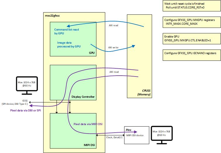
MIPI DSI host controller
The MIPI DSI host controller takes input from the display controller in the form of DPI or DBI signals. This is translated into the standard MIPI DSI format to be sent to the MIPI DPHY.
Reset
Rstz input to PHY - This is used to place the digital section of the PHY in reset state
Shutdownz input to PHY - This is used to place the PHY in shutdown. All analog blocks are in shutdown mode and the digital logic is reset.
Clocks
Clock | Frequency | Usage |
|---|---|---|
rxclkesc | 20 MHz (Max) | Provided by the connected DSI device via data lane 0. Domain for RX Escape Mode logic |
txclkesc | 20 MHz (Max) | TX escape mode clock. Divided version of lanebyteclk |
lanebyteclk | 187.5 MHz | Internally generated from PLL. Domain for the DSI Host Controller core logic. Frequency is 1/8 of the bit rate on MIPI-DSI data lanes in high-speed mode (1.5Gbps) |
pclk | 100 MHz | Connected to APB interface of DSI controller |
dbiclk | 37.5 MHz (Max) | Data clock for DBI Type B via MIPI-DSI. |
dpiclk | 1-64 MHz | Pixel clock for DPI via MIPI-DSI. |
clk_ref_mipidsi | 1/8 bit rate of the MIPI-DSI data lanes in high-speed mode | Lane Byte Clock |
MIPI DPHY
PSOC™ Edge
has a built-in MIPI DPHY with 2 TX lanes that implement the physical layer. The PHY has two data lanes and one clock lane. The effective bit rate of the two lanes is 1.5 Gbps per lane. Each of the clock and data lines are a differential pair of positive and negative lines.
Physical I/O connections
The DPHY has two TX lanes and a clock lane coming from the PLL. . The signals are listed in the following table (refer to the
data sheet
for specific pin numbers):
Port name | Description |
|---|---|
DSI.REXT | External resistor connection Use a 200 ohm resistor to ground |
DSI.CLKP | Positive D-PHY Differential Clock Line |
DSI.CLKN | Negative D-PHY Differential Clock Line |
DSI.DATA0P | Positive D-PHY Differential Data Line, Lane 0 |
DSI.DATA0N | Negative D-PHY Differential Data Line, Lane 0 |
DSI.DATA1P | Positive D-PHY Differential Data Line, Lane 1 |
DSI.DATA1N | Negative D-PHY Differential Data Line, Lane 1 |
External reference resistor:
The usage of the external termination resistor is mandatory. The termination resistor is used on the calibration procedures during D-PHY start-up—for smaller TX termination value spread after calibration—and it can be disconnected after calibration. Connect the DSI.REXT pin to a 200 Ω resistor to ground.
Features
DPI-2 and DBI-2 Type B displays via DSI
Up to 2 data lanes, maximum 1.5 Gbps per lane
PLL for high-speed mode clock generation
Generic command interface (DCS and proprietary read & write)
Video pattern generator
Ultra-Low-Power mode with disabled PLL
Tearing effect interrupt for DBI displays
Shutdown and Color Mode control for DPI displays. The DSI host controller and DPHY conforms to the following standards:
MIPI Alliance Specification for Display Serial Interface (DSI) Version 1.2
- 16 June 2014
MIPI Alliance Standard for Display Bus Interface v2.00 (DBI-2) - 16 Nov 2005
MIPI® Alliance Specification for Display Command Set (DCS) Version 1.3 - 5 October 2015
MIPI Alliance Standard for Display Pixel Interface v2.00 (DPI-2) - 15 September 2005
MIPI Alliance Specification for Stereoscopic Display Formats (SDF) v1.0 - 22 November 2011
MIPI Alliance Specification for D-PHY v1.2, 01 August 2014
MIPI Alliance Specification for C-PHY v1.0, October 2014
AMBA 2.0 Specification (APB) from Arm®
VESA Display Stream Compression (DSC) Standard Version 1.1 - 1 August 2014
Host controller
The MIPI DSI host controller takes input from the display controller in the form of a DPI or DBI signal. This is translated into the standard MIPI DSI format to be sent to the MIPI DPHY.
Figure 469
shows the layout of the block along with its internal connects from the Display Controller (DC), internal connections to the host bus, and the external connects to a display.
Figure 469.
MIPI DSI host block
Initialization
The initialization of the MIPI DSI host controller is done using the MIPI DSI Driver APIs. The API Cy_MIPIDSI_Init is used to initialize the MIPI DSI host and the attached DPHY. The CY_GFFXSS_Init function initializes the entire graphics pipeline including the host controller and DPHY. Refer to the API Reference guide for more information on the APIs. The DCNANO APIs are lower level than the Infineon-provided APIs, and these can be used to configure the block directly. But it is recommended to use the high-level APIs provided by Infineon.
Reset
Rstz
input to PHY:
This is used to place the digital section of the PHY in reset state
Shutdownz input to PHY:
This is used to place the PHY in shutdown. All analog blocks are in shutdown mode and the digital logic is reset.
Testclr:
DPHY Test and Control Interface clear
Clocks
Clock | Frequency | Usage |
|---|---|---|
rxclkesc | 20 MHz (Max) | Provided by the connected DSI device via data lane 0. Domain for RX Escape Mode logic |
txclkesc | 20 MHz (Max) | TX escape mode clock. Divided version of lanebyteclk |
lanebyteclk | 187.5 MHz | Internally generated from PLL. Domain for the DSI Host Controller core logic. Frequency is 1/8 of the bit rate on MIPI-DSI data lanes in high-speed mode (1.5 Gbps) |
pclk | 100 MHz | Connected to APB interface of DSI controller |
DPHY
PSOC™ Edge
has a built-in MIPI DPHY with 2 TX lanes that implements the physical layer. The PHY has two data lanes and one clock lane. The effective bit rate of the two lanes is 1.5 Gbps per lane. Each of the clock and data lines are a differential pare.
Initialization
Initializing D-PHY
This process is based on the APB register interface access, and it is only valid when used with the D-PHY.
Figure 470.
DPHY initialization flow
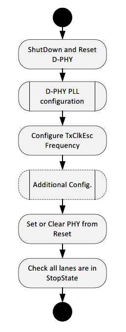
Power-up and reset the PHY using “PHY_RSTZ” register
TxClkEsc frequency must be configured between 2 to 20 MHz. This is done by writing into the tx_esc_clk_division field of the CLKMGR_CFG register. The tx_esc_clk_division field divides the byte clock, and generates a TX_ESC clock for the D-PHY. Figure 471 describes how txclkesc is obtained.
Figure 471.
DPHY clock generation
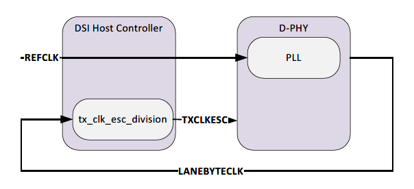
Clear phy_shutdownz (PHY_RSTZ0) and phy_rstz (PHY_RSTZ1) to put the PHY in the reset state. Set phy_shutdownz (PHY_RSTZ0) and phy_rstz (PHY_RSTZ1) to remove the PHY from reset state
Verify that D-PHY active lanes are in Stop state:
q PHY_STATUS2 = 1'b1
q PHY_STATUS[4] = 1'b1
q PHY_STATUS[7] = 1'b1 – if Lane 2 active
q PHY_STATUS[9] = 1'b1 – if Lane 3 active
q PHY_STATUS[11] = 1'b1 – if Lane 4 active
Video mode pattern generator
The MIPI DSI host can transmit a color bar pattern without horizontal or vertical color bar and D-PHY BER testing pattern without any kind of stimulation. Follow the programming sequence shown in the following figure to send a test pattern.
Video mode pattern generator flow diagram
Configure the MODE_CFG register to enable video mode. Configure the video mode type using VID_MODE_CFG[1:0] configuration pins
Configure the DPI_COLOR_CODING register
Configure the frame using the registers shown in the Figure 473 figure
Configure the pattern generation mode (VID_MODE_CFG20) and pattern orientation (VID_MODE_CFG[24]) and enable it (VID_MODE_CFG16)
Figure 472.
DPHY video mode pattern generator flow
Figure 473.
Configuring the Frame
Physical I/O connections
The DPHY has two TX lanes and a clock lane coming from the PLL. All of these lanes are differential. The signals are listed in the following figure (refer to the data sheet for specific pin numbers).
Port name | Description |
|---|---|
pad_dphy_rext | External resistor connection Use a 200-ohm resistor to ground |
pad_dphy_atb | Analog test bus pin |
pad_dphy_clk_p | Positive D-PHY Differential Clock Line |
pad_dphy_clk_n | Negative D-PHY Differential Clock Line |
pad_dphy_data0_n | Positive D-PHY Differential Data Line, Lane 0 |
pad_dphy_data0_p | Negative D-PHY Differential Data Line, Lane 0 |
pad_dphy_data1_n | Positive D-PHY Differential Data Line, Lane 1 |
pad_dphy_data1_p | Negative D-PHY Differential Data Line, Lane 1 |
External reference resistor
The usage of the external termination resistor is mandatory. The termination resistor is used on the calibration procedures during D-PHY start-up—for smaller TX termination value spread after calibration—and it can be disconnected after calibration.
Autonomous analog
Introduction
Autonomous Analog is a low-power, reconfigurable, mixed-signal, sensing, conditioning, and response system that operates independently of the CPU.
Features
Two continuous-time blocks (CTBs), each consisting of two opamp circuits that can perform analog front-end functions such as:
Programmable Gain Amplifier (PGA)
Transimpedance Amplifier (TIA)
Pseudo-Differential Amplifier
Unity Gain Buffer (Voltage Follower)
Open Loop Opamp
Comparator
One SAR ADC with
12- to 20-bit (with accumulation) results
5-Msps sample rate at 12 bits or 250 ksps at 16 bits in System High Performance mode
200-ksps sample rate at 12 bits or 12.5 ksps at 16 bits in System Deep-Sleep mode
Buffered Inputs
Inputs from 16 pins or 7 internal signals (from opamps, DACs, temperature sensor etc.)
Simultaneous sampling of as many as 10 inputs
32 logical channels
Post processing and storage
Accumulation and averaging – 2x,4x, 8x … 256x
Two 64-tap FIR filters
A 512-entry FIFO that can subdivided into 2, 4 or 8 FIFOs
Limit detection
Offset and gain calibration
Two 12-bit DACs with
1-μS refresh time
Buffered outputs (Sample and Hold capable)
A 512-entry waveform table
Automatic waveform generation
Two Programmable Threshold Comparators (PTComps) with post‑processing that supports Audio Activity Detection (AAD) and Motor Control
Two 4-bit Programmable Reference Blocks (PRB)
A Finite-State Machine (FSM) sequencer called the Autonomous Controller that works with a 64-entry State Transition Table (STT), to transition appropriately through various pre-defined states, based on Timer, and/or Events. The Autonomous Controller can perform the following functions in Device DeepSleep Mode:
Power cycling of individual blocks
Listen to/send triggers to individual blocks
Send triggers and/or interrupts to the CPU
Change the connections between blocks using dynamic configurations of individual blocks
Digital output to as many as four GPIOs
Architecture
Figure 474.
Autonomous analog block diagram
shows the overall block diagram of the Autonomous Analog. Note that the run-time control activities such as enabling or disabling blocks, changing the power modes of the blocks, switching inputs/routing, waiting for ADC scan to finish, and triggering the DAC etc are done by the Always-On Autonomous Controller independent of the CPU. For this purpose, most analog blocks in Autonomous Analog have a static configuration (unchanged by the Autonomous Controller during run-time) and a Dynamic Configuration (can be changed by the Autonomous Controller during run-time). The details of Autonomous Analog Configuration options are given in
Table 499
.
Configuration | Registers | Number of maximum configurations | Comments |
|---|---|---|---|
Static configuration | <block>STA_CFG Registers In the case of SAR ADC, FIR configuration registers are included in the static configuration structures. | 1 | Configuration that is set before starting the Autonomous Control. These settings cannot be changed during Deep Sleep and requires the autonomous controller to be stopped by the CPU before reconfiguring. |
Dynamic configuration | <block>DYN_CFG registers | 4-8 | Configuration that can be switched dynamically (during the run time) by the Autonomous Controller. These settings can be switched in the Deep Sleep power mode. |
SAR Sequencer Table | SAR_STT_HS/LS_DATA registers | 32 | SAR sequencer tables |
State Transition Table | ACTRLR _TIMER_TABLE_STRUCT registers | 64 | State Transition Table controls the states and transitions of the Autonomous Controller. Several block settings are available in the State Transition Table bit fields itself so that these can be changed without loading a new dynamic configuration. |
The firmware is expected to configure the Autonomous Analog in the following order:
Enable the system and peripheral clocks required for the Autonomous Analog
Enable the Autonomous Analog using the ACTRLR_CTRL register
Set up Static Configurations for each block, including DAC waveform tables, FIR filters, FIFOs etc
Set up Dynamic Configurations that control inputs/outputs and routing during the run-time
Set up State Transition Table and the SAR Sequencer Table. Enabling/Disabling individual blocks, controlling PGA/TIA gain, triggering ADC/DAC etc must be set up in the State Transition Table
Run the Autonomous Controller using ACTRLR_CMD register
Once the Autonomous Controller starts running, it takes over the control the individual blocks and sequences through the states defined in the State Transition Table. The firmware can interact with the Autonomous Controller using triggers and interrupts. The firmware can also read the results produced by the individual blocks, independent of the Autonomous Controller.
For more details, see
Figure 501
Continuous time block (CTB)
Continuous-Time Blocks (CTB) consist of opamp circuits that can perform analog front-end functions.
Autonomous-Analog in this product line has two CTBs, each consisting of two opamps, feedback resistor networks, and multiplexers that can form topologies such as:
Programmable Gain Amplifier (PGA)
Trans-impedance Amplifier (TIA)
Pseudo-Differential Amplifier
Unity Gain Buffer (Voltage Follower)
Open Loop Opamp
Comparator
Static configuration
, which uses CTB0 as an example, shows the static configuration options available for the CTB, controlled by the bit-fields in CTBLx_STAT_CFG_CFG register. See the device datasheet for exact pin connections.
Figure 475.
CTB static configuration
The bit field OAx_PWR_MODE controls the current consumption, gain-bandwidth, input range, and drive strength of the opamps as
Table 500
shows. The opamp specifications in the following table provide guidelines to choose a specific power mode. See the device datasheet for the exact opamp specifications in each power mode.
OAx_PWR_MODE Value | Power Mode | Opamp specifications | ||||
|---|---|---|---|---|---|---|
Current Consumption (I DD ) | Unity-Gain Bandwidth (GBW) | Input Range | Max Output Current (Output to Pin) | |||
Output to Pin | Internal Drive | |||||
1 | ULTRA_LOW | 15 µA | 100 kHz | 30 kHz | 0 to V DDA -1 V | 10 µA |
2 | ULTRA_LOW_RAIL | 35 µA | 100 kHz | 30 kHz | 0 to V DDA -0.2 V | 10 µA |
4 | LOW_RAIL | 150 µA | 1.2 MHz | 350 kHz | 0 to V DDA -0.2 V | 100 µA |
6 | MEDIUM_RAIL | 300 µA | 2.4 MHz | 700 kHz | 0 to V DDA -0.2 V | 1 mA |
8 | HIGH_RAIL | 800 µA | 6 MHz | 1.75 MHz | 0 to V DDA -0.2 V | 1 mA |
10 | ULTRA_HIGH_RAIL | 1.3 mA | 7.5 MHz | 2.8 MHz | 0 to V DDA -0.2 V | 10 mA |
The bit field OAx_TOPO controls the topology of the opamp as
Table 501
shows. The gain of topologies such as PGA, TIA, and the differential amplifier are set directly from the State Transition Table of the
Autonomous controller
.
OAx_TOPO Field Value | Topology | Description | Gain |
|---|---|---|---|
0 | Comparator | Comparator with no hysteresis Comparator can generate a trigger that can be polled by the Autonomous Controller or routed to other peripherals. Comparator can also generate interrupts to the CPU. OAx_COMP_OUT field controls the nature of interrupt/trigger generation. | N/A |
1 | PGA | Programmable Gain Amplifier (PGA) | Inverting gain: 0.42 to 31 Non-inverting gain: 1.42 to 32 Set by the Autonomous Controller during run-time (CTBLx_OAx_GAIN fields in the State Transition Table register TT_CFG2) |
2 | TIA | Trans-impedance Amplifier (TIA) | 57kΩ to 186kΩ Set by the Autonomous Controller during run-time (CTBLx_OAx_GAIN fields in the State Transition Table register TT_CFG2) |
3 | Open-Loop Opamp | Open-Loop Opamp (topology set by external feedback circuit) | Set by external feedback circuit |
4 | Differential Amplifier | Pseudo-Differential Amplifier (first stage of an instrumentation amplifier). Same topology and gain must be set for both opamps. | 0.42 to 31 Set by the Autonomous Controller during run-time (CTBLx_OAx_GAIN fields in the State Transition Table register TT_CFG2) |
5 | Hysteric Comparator | Comparator with hysteresis. See the device datasheet for hysteresis value. Comparator can generate a trigger that can be polled by the Autonomous Controller or routed to other peripherals. Comparator can also generate interrupts to the CPU. OAx_COMP_OUT field controls the nature of interrupt/trigger generation. | N/A |
6 | Buffer | Unity-gain buffer (voltage-follower) | 1 |
See the CTBLx_STAT_CFG_CFG register in the Registers TRM for additional details of CTB static configuration.
Dynamic configuration
The input and output connections of the CTBs are controlled by multiplexers (muxes) that are available as dynamic configurations.
Figure 476
which uses CTB0 OA0 as an example, shows the dynamic configurations of a CTB opamp. Eight dynamic configurations can be created
on a per-opamp basis
and switched at run-time by the
Autonomous controller
(CTBLx_OAx_CFG fields in the State Transition Table register TT_CFG2) .
Figure 476
also shows the bit fields in the CTBLx_DYN_CFG_STRUCT_OA_MUX_CFG registers that set up the dynamic configuration of the opamps.
Figure 476.
Dynamic configuration of Opamp (1/2 of CTB)
See the corresponding register descriptions in the Registers Technical Manual for more information. See the device datasheet for exact pin connections.
The following figures show the valid dynamic configurations for each opamp topology.
Figure 477.
PGA dynamic configuration
All the muxes are valid in a PGA dynamic configuration. However, in a typical PGA circuit, the inverting terminal of the opamp is left unconnected. Other input terminals are connected as follows:
Non-Inverting PGA:
Input is connected to the non-inverting terminal using OA_INP_DIRECT, OA_INP_REF, or CTBBUS_MUX_IN/CTBBUS_MUX_OUT muxes. The resistor terminal is connected to the analog ground (typically V DDA /2, to get equal positive and negative output swings), which can be supplied from:
A pin, routed using the OA_RES_DIRECT or CTBBUS_MUX_IN/CTBBUS_MUX_OUT muxes
Buffered DAC0 or DAC1 output, routed using the OA_RES_REF mux.
Do not connect an unbuffered DAC output
to the resistor terminal of the PGA
PRB_OUT0, PRB_OUT1, VBGR(0.9V) or an external voltage buffered by one of the opamps in the other CTB, routed using OA_RES_REF mux
Inverting PGA:
Input is connected to the resistor terminal using OA_RES_DIRECT, OA_RES_REF, or CTBBUS_MUX_IN/CTBBUS_MUX_OUT muxes.
Do not connect an unbuffered DAC output
to the resistor terminal of the PGA. Non-inverting terminal is connected to the analog ground (typically V DDA /2, to get equal positive and negative output swings), which can be supplied from:
A pin, routed using the OA_INP_DIRECT or CTBBUS_MUX_IN/CTBBUS_MUX_OUT muxes
PRB_OUT0, PRB_OUT1, VBGR(0.9V), DAC0, or DAC1 routed using the OA_INP_REF mux
Figure 478.
TIA dynamic configuration
TIA is a current to voltage converter. Input current is supplied from a pin to the inverting terminal using OA_INM_DIRECT,or CTBBUS_MUX_IN/CTBBUS_MUX_OUT muxes. A non-inverting terminal is connected to the analog ground (typically V
DDA
/2, to get equal positive and negative output swings), which can be supplied from:
A pin, routed using the OA_INP_DIRECT or CTBBUS_MUX_IN/CTBBUS_MUX_OUT muxes
PRB_OUT0, PRB_OUT1, VBGR(0.9V), DAC0, or DAC1 routed using the OA_INP_REF mux
Figure 479.
Buffer dynamic configuration
In a typical unity gain buffer/voltage-follower application, an inverting terminal is unconnected and the input is connected to the non-inverting terminal using OA_INP_DIRECT, OA_INP_REF or CTBBUS_MUX_IN/CTBBUS_MUX_OUT muxes.
Figure 480.
Open-loop dynamic configuration
This topology is an open-loop opamp without internal feedback (resistor ladder is disconnected). Use the available muxes to provide inputs and feedback. Always connect the output to a pin by setting the OA_TO_PIN field to '1'.
Figure 481.
Comparator dynamic configuration
Figure 482.
Hysteric Comparator dynamic configuration
Comparator and Hysteric Comparator topologies have no analog output. These topologies produce a digital output in the form of a Trigger/Interrupt. These topologies are used to compare an input with another input or a reference.
Figure 483.
Differential dynamic configuration
The pseudo-differential amplifier is a differential-input/differential output topology. Therefore, it uses both the CTB opamps. It can be used to form the first stage of an instrumentation amplifier or to add gain to a differential input of the ADC. In a typical application, inverting and resistor terminals of both the opamps are left unconnected. The differential input is connected between the non-inverting terminals of OA0 and OA1 via the OA_INP_DIRECT, OA_INP_REF or CTBBUS_MUX_IN/CTBBUS_MUX_OUT muxes of each opamp. Creating separate dynamic configurations for each opamp is required if OA_INP_REF or CTBBUS_MUX_IN/CTBBUS_MUX_OUT muxes are used to route the inputs.
Opamp compensation
To ensure the stability of the opamp circuits, compensate the opamps with the following:
Enable the internal compensation capacitor (CC) of the opamps by setting the OA0_CC_ENABLE/OA1_CC_ENABLE bits in the CTBLx_STAT_CFG_CFG register to "ENABLE"
Set proper CC values using CTBL_TRIM_STRUCTx.OAx_COMP_TRIM registers
PGA and differential topologies have an additional feedback compensation capacitor (C_FB) that is controlled by the C0_FB/C1_FB bit fields in the CTBLx_STAT_CFG_CFG registers. The following tables show the recommended CC and C_FB settings based on the topology, power mode, output to pin, and gain settings.
Uncompensated/under-compensated opamps may offer higher GBW than the typical values in
Table 500
. However, it is important to test and verify the stability of the opamp circuit as unity-gain stability is not guaranteed for uncompensated/under-compensated opamps.
Output to pin | Power mode | Compensation setting CC |
|---|---|---|
Yes/Dynamic Maximum load capacitance = 50pF | ULTRA_LOW, ULTRA_LOW_RAIL, LOW_RAIL, or MEDIUM_RAIL | 2 |
HIGH_RAIL or ULTRA_HIGH_RAIL | 5 | |
No | ULTRA_LOW, ULTRA_LOW_RAIL, LOW_RAIL, or MEDIUM_RAIL | 4 |
HIGH_RAIL or ULTRA_HIGH_RAIL | 5 |
Output to pin | Power mode | Lowest gain setting in the State Transition Table (Non-inverting) | Compensation settings | |
|---|---|---|---|---|
CC | C_FB | |||
Yes/Dynamic Maximum load capacitance = 50pF | ULTRA_HIGH_RAIL | >=8 | 2 | 1 |
<8 | 2 | 2 | ||
HIGH_RAIL | >=16 | 2 | 1 | |
<16 | 2 | 2 | ||
MEDIUM_RAIL, LOW_RAIL, ULTRA_LOW, or ULTRA_LOW_RAIL | >=4 | 2 | 1 | |
<4 | 2 | 4 | ||
No | ULTRA_HIGH_RAIL or HIGH_RAIL | >=4 | 6 | 1 |
<4 | 6 | 4 | ||
MEDIUM_RAIL or LOW_RAIL | >=4 | 5 | 1 | |
<4 | 5 | 4 | ||
ULTRA_LOW, or ULTRA_LOW_RAIL | >=4 | 3 | 1 | |
<4 | 3 | 4 | ||
SAR ADC
Autonomous analog in this product line has a SAR ADC with the following features:
12- to 20-bit (with accumulation) results
5-Msps sample rate at 12 bits or 250-ksps at 16 bits in System High Performance mode (HS mode ADC)
200-ksps sample rate at 12 bits or 12.5-ksps at 16 bits in System Deep Sleep mode (LP mode ADC)
Buffered Inputs
Inputs from 16 pins or 7 internal signals (from opamps, DACs, temperature sensor etc.)
Simultaneous sampling of as many as 10 inputs
32 logical channels
Post processing and storage
Accumulation and averaging – 2x,4x, 8x … 256x
Two 64-tap FIR filters
A 512-entry FIFO that can be subdivided into 2, 4, or 8 FIFOs
Limit detection
Offset and gain calibration
Static configuration
The SAR ADC has two operating modes: a differential, Deep-Sleep capable, Low-Power (LP) mode and a single-ended High-Speed (HS) mode that's available only in System High Performance mode. The LP ADC is limited to 200 ksps while the HS ADC can achieve 5 Msps. Only one of these cores are active at a time, based on the LP/HS mode selection at the Autonomous Analog level. The ADC's operating mode is controlled by the
Autonomous controller
's LP/HS mode selection in the State Transition table. This mode selection must be done in the first state of the State Transition table - run-time switching between LP and HS modes is not supported.
Static configuration of the ADC is controlled by the LPPASS_SAR_STA_CFG registers.
Figure 484.
SAR ADC static configuration in LP mode
The LP mode uses a fully-differential, Deep-Sleep capable, Low-Power (LP) ADC core that runs from the 4-MHz Low Power Oscillator (LPOSC) inside the Autonomous Analog. This mode can achieve a maximum sample rate of 200 ksps at 12 bits.
The LP ADC also supports single-ended operation with CTRL.LP_DIFFERENTIAL_EN bit set to "DISABLED". In this configuration, the V
MINUS
(non-inverting ADC input) is connected to the reference voltage V
REF
(LP) of the ADC as
Figure 485
shows.
Figure 485.
SAR ADC static configuration in LP mode, single-ended
Figure 486.
SAR ADC static configuration in HS mode
The HS mode uses a single-ended, High-Performance (HP) ADC core that runs from the 80-MHz CLK_HF9 from the system resources. This mode can achieve a maximum sample rate of 5 Msps at 12 bits.
Note:
The HS core is always single-ended and behaves differently to the LP core in single-ended mode for the V
REF
. See
Output data format
for more details.
The CTRL.LP_VREF_SEL and HS_VREF_SEL bit fields set the reference voltage of LP ADC and HS ADC respectively.
LP_VREF_SEL/HS_VREF_SEL | Reference Name | Description |
|---|---|---|
0 | V DDA | The analog-supply voltage of the device. Do not use this option in LP ADC's single-ended operation |
1 | External V REF | External reference voltage from the VREF pin of the device In the HS mode, connect a bypass capacitor to this pin if external V REF is not used See the device datasheet for the exact location of this pin and the capacitance value |
2 | VBGR | Internal 0.9-V bandgap reference |
3 | V DDA /2 | Half the analog-supply voltage of the device |
4 | PRB_OUT0 | Outputs of the Programmable reference block (PRB) (PRB) |
5 | PRB_OUT1 |
The LP and HS ADC can take inputs from one of the 16 mux channels – channels that are configured using a pair of input muxes and buffers. CTRL.BUF0_PWR_MODE/BUF1_PWR_MODE bit fields set the power and bandwidth of these buffers. As many as 16 Mux channels can be defined using the registers MUX_CHAN_CFG0-15.
Mux channels can take inputs from the following list of 24 signals:
Eight dedicated GPIO pins
Eight CTB0/1 port pins
Four opamp outputs
Two DAC outputs
Internal temperature sensor
V SSA
POS_MUX_SEL/NEG_MUX_SEL | Input | Description |
|---|---|---|
0 | CTB0 PIN 1 | Input from CTB0 Port Pin 1 (aanalog.ctb0.1) |
1 | CTB0 PIN 4 | Input from CTB0 Port Pin 4 (aanalog.ctb0.4) |
2 | CTB0 PIN 6 | Input from CTB0 Port Pin 6 (aanalog.ctb0.6) |
3 | CTB0 PIN 7 | Input from CTB0 Port Pin 7 (aanalog.ctb0.7) |
4 | CTB1 PIN 1 | Input from CTB1 Port Pin 1 (aanalog.ctb1.1) |
5 | CTB1 PIN 4 | Input from CTB1 Port Pin 4 (aanalog.ctb1.4) |
6 | CTB1 PIN 6 | Input from CTB1 Port Pin 6 (aanalog.ctb1.6) |
7 | CTB1 PIN 7 | Input from CTB1 Port Pin 7 (aanalog.ctb1.7) |
8 | CTB0 OA0 OUT | CTB0 Opamp 0's output |
9 | CTB0 OA1 OUT | CTB0 Opamp 1's output |
10 | CTB1 OA0 OUT | CTB1 Opamp 0's output |
11 | CTB1 OA1 OUT | CTB1 Opamp 1's output |
12 | DAC0 | DAC0's output |
13 | DAC1 | DAC1's output |
14 | TEMP SENSOR+/- | Internal temperature sensor's output |
15 | SAR PIN 0 | Input from SAR Port Pin 0 (aanalog.sar0) |
16 | SAR PIN 1 | Input from SAR Port Pin 1 (aanalog.sar1) |
17 | SAR PIN 2 | Input from SAR Port Pin 2 (aanalog.sar2) |
18 | SAR PIN 3 | Input from SAR Port Pin 3 (aanalog.sar3) |
19 | SAR PIN 4 | Input from SAR Port Pin 4 (aanalog.sar4) |
20 | SAR PIN 5 | Input from SAR Port Pin 5 (aanalog.sar5) |
21 | SAR PIN 6 | Input from SAR Port Pin 6 (aanalog.sar6) |
22 | SAR PIN 7 | Input from SAR Port Pin 7 (aanalog.sar7) |
24 | VSSA | Ground from V SSA |
See the Device Datasheet for the exact location of SAR and CTB pins.
MUX_CHAN_CFG0-15 also contains an option to bypass the buffers for a specific channel using the BUF_BYPASS bit field. If this option is enabled for a specific channel, the user must make sure that the respective input has enough drive strength to directly drive the ADC input.
The HS ADC can additionally take inputs from GPIO channels - 8 dedicated single-ended input channels directly connected to 8 dedicated samples, allowing simultaneous sampling. As many as 8 GPIO channels can be defined using the registers GPIO_CHAN_CFG0-7.
POS_PIN/NEG_PIN | Input | Description |
|---|---|---|
0 | SAR PIN 0 | Input from SAR Port Pin 0 (aanalog.sar0) |
1 | SAR PIN 1 | Input from SAR Port Pin 1 (aanalog.sar1) |
2 | SAR PIN 2 | Input from SAR Port Pin 2 (aanalog.sar2) |
3 | SAR PIN 3 | Input from SAR Port Pin 3 (aanalog.sar3) |
4 | SAR PIN 4 | Input from SAR Port Pin 4 (aanalog.sar4) |
5 | SAR PIN 5 | Input from SAR Port Pin 5 (aanalog.sar5) |
6 | SAR PIN 6 | Input from SAR Port Pin 6 (aanalog.sar6) |
7 | SAR PIN 7 | Input from SAR Port Pin 7 (aanalog.sar7) |
Combined with two samplers for mux channels, the HS mode can simultaneously sample 10 inputs.
The ADC does not have dynamic configurations. Instead, the channel settings using MUX_CHAN_CFG0-15 and/or GPIO_CHAN_CFG0-7 registers, together with the sequencer table entries in SEQ_LP_DATA or SEQ_HS_DATA registers, control the input muxing and scanning during run-time.
Post-processing and storage
shows the digital post-processing and data storage options available for both the LP and HS ADCs. For the LP ADC, these options are available in the device Deep Sleep mode.
Post-Processing/Storage option | Description | Configuration | How to enable for a specific channel |
|---|---|---|---|
Accumulation and averaging | Accumulate or average (accumulate and shift) several conversions to increase the numerical/effective resolution of the ADC | SAR sequencer table enables and selects the number of samples to be accumulated. See Output data format Shifting is controlled by the following bit fields of Mux/GPIO channels
| |
Sign extension | Select signed or unsigned result for a given channel | N/A - depends on the ADC and input mode. See Output data format | Controlled by the following bit fields of Mux/GPIO channels
|
Offset and Gain Correction | Add offset and gain correction for a given channel | Set up as many as 8 offset and gain coefficients using CHAN_COEFF0-7 registers | By selection one of the 8 coefficients using the following bit fields of Mux/GPIO channels
|
Limit Detection | Generates triggers/interrupts when a channel or FIR result is above/below a threshold or inside/outside two thresholds | STATUS_CFG0-3 registers select Above,Below,Inside or Outside conditions. STATUS_RANGE_LOW0-3 and STATUS_RANGE_HIGH0-3 registers select corresponding thresholds | By selecting one of the STATUS_STRUCT_x options for the following bit fields of mux/GPIO channels or FIR filter
|
Channel ID | Include channel number identifier in the most significant byte of channel results (31:24) stored in FIFO. See Output data format | CTRL.CHAN_ID_EN bit field | N/A - all mux and GPIO channels are affected |
FIR filtering | Finite impulse response (FIR) filtering of channel results with as many as 64 taps | Set up the number of taps and data format using FIR_CONFIG0/1 registers Load the filter coefficients to SAR_FIR0_STRUCT0-63 and/or SAR_FIR1_STRUCT0-63 registers | Select one of the channels as the input of the filter using FIR_CONFIGx.CHANNEL_SEL fields |
FIFO Storage | Store channel results to FIFO memory | Configure the number of FIFOs using LPPASS_MMIO_FIFO_STA_CFG registers | By selecting one of the FIFOs using the following bit fields of Mux/GPIO channels or FIR filter
|
See the corresponding register descriptions in the Registers reference manual for more information.
Low-Power (LP) ADC sampling and scan
The LP ADC is limited to 200 ksps. However, the LP ADC can scan and process data in the device Deep Sleep power mode.
To set up the LP ADC, follow these steps:
Choose the LP mode of operation for the Autonomous controller (LP/HS mode selection in the State Transition table). Select this mode in the first state of the State Transition table - run-time switching between LP and HS modes is not supported
Set up Static configuration for the LP ADC, including the following:
16 mux channels using MUX_CHAN_CFG0-15 registers
Four global sample times using the LP_SAMPLE_TIME field in registers SAMPLE_TIME0-3. Minimum sample time is 6 cycles
Optional: Post-processing and storage (Accumulation, FIR, FIFO etc)
Create 32 sequencer table entries using SEQ_LP_DATA0-31 registers, depending on the application. In each sequencer table entry, do the following:
Set LP_CHAN_EN bit
Select one of the mux channels to scan using the CHAN_SEL field
Select one of the four global sample times using SAMPLE_TIME_SEL, and set SAMPLE_TIME_EN bit
Optional: Set up Accumulation using AVG_CNT and AVG_EN fields (See Output data format )
Select an action using the NEXT_ACTION field
If additional channels need to be scanned sequentially, set NEXT_ACTION to “GO_TO_NEXT”. In this case, follow the above step to set up subsequent SEQ_LP_DATA registers for additional scans
If this is the final SEQ_LP_DATA register entry, select “NEXT_ACTION” as “STOP” for a single (one-shot) scan or “GO_TO_ENTRY_ADDR” for continuous scans
The ADC starts scanning once it receives a trigger from the
Autonomous controller
’s State Transition table. Make sure that the correct entry address (SEQ_LP_DATA register index) is selected in the State Transition table.
Figure 487.
SAR ADC Timing - LP
shows the timing of the LP ADC scanning a single channel continuously or multiple channels sequentially. The LP ADC requires a minimum of 6 cycles for sampling and 14 cycles for conversion. Therefore,
The maximum throughput of LP ADC = 4.096 MHz / (14+6 cycles) = 204.8 ksps
Note:
Accumulating "N" samples reduces the throughput by a factor of N. For example, accumulating 16 samples to get 4 extra bits of numerical resolution (resolution increases from 12-bits to 16-bits) reduces the throughput to (204.8/16) = 12.8 ksps.
High-Speed (HS) ADC sampling and scan
The HS Mode can reach 5 Msps with simultaneous sampling or 4 Msps with sequential sampling. However, with HS Mode, the ADC can scan and process data only in the device Active power mode.
To set up the HS ADC, follow these steps:
Choose HS mode of operation for the Autonomous controller (LP/HS mode selection in the State Transition table). Select this mode in the first state of the State Transition table - run-time switching between LP and HS modes is not supported
Set up Static configuration for the HS ADC, including the following features:
Eight GPIO channels using GPIO_CHAN_CFG0-7 registers and/or 16 mux channels using MUX_CHAN_CFG0-15 registers
Four global sample times using the HS_SAMPLE_TIME field in registers SAMPLE_TIME0-3. Minimum sample time is 6 cycles for GPIO channels or a single, static mux channel. If multiple mux channels are included in a scan, then the sampling time of the mux channels must be at least 32 cycles
Optional: Post-processing and storage (Accumulation, FIR, FIFO etc)
Create 32 sequencer table entries using SEQ_HS_DATA0-31 registers, depending on the application. In each sequencer table entry, do the following:
If required, enable one or more GPIO channels to be scanned using the HS_GPIO_CHAN_EN field
Note:
If multiple channels are enabled, these are sampled simultaneously
If required, enable a mux channel using the HS_MUX_CHAN_EN_SEL bit field and select the inverting and non-inverting mux channels using MUX0_CHAN_SEL and MUX1_CHAN_SEL fields
Select one of the four global sample times using SAMPLE_TIME_SEL, and set SAMPLE_TIME_EN bit
Optional: Set up Accumulation using the AVG_CNT and AVG_EN fields (See
Output data format
)
Select an action using the NEXT_ACTION field
If additional channels need to be scanned sequentially, set NEXT_ACTION to “GO_TO_NEXT”. In this case, follow the above step to set up subsequent SEQ_HS_DATA registers for additional scans
If this is the final SEQ_HS_DATA register entry, select “NEXT_ACTION” as “STOP” for a single (one-shot) scan or “GO_TO_ENTRY_ADDR” for continuous scans
The ADC starts scanning once it receives a trigger from the
Autonomous controller
’s State Transition table. Make sure that the correct entry address (SEQ_LP_DATA register index) is selected in the State Transition table.
Figure 488.
SAR ADC Timing - HS, Sequential
shows the timing of the HS ADC scanning a single channel continuously, or sequentially scanning multiple channels. For sequential scanning, the HS ADC requires a minimum of 4 cycles for sampling and 16 cycles for conversion. Therefore,
The maximum throughput of HS ADC for sequential sampling = 80 MHz / (16+4 cycles) = 4 Msps
Note:
Accumulating "N" samples reduces the throughput by a factor of N. For example, accumulating 16 samples to get 4 extra bits of numerical resolution (resolution increases from 12-bits to 16-bits) reduces the throughput to (4000/16) = 250 ksps.
Figure 489.
SAR ADC Timing - HS, Simultaneous
shows the timing of the HS ADC scanning multiple channels sequentially. For sequential scanning, the HS ADC also requires a minimum of 4 cycles for sampling and 16 cycles for conversion. However, sampling of one channel can overlap with the conversion of other channels. Therefore, if a minimum of two channels are scanned sequentially, and the sampling times of both the channels are equal to or below 16 cycles,
The maximum throughput of HS ADC for simultaneous sampling = 80 MHz/16 cycles = 5 Msps
Output data format
Result registers and FIFO entries are always 32-bit (zero or sign-extended, depending on the signed/unsigned result settings respectively). If the CHAN_ID_EN bit field in the CTRL register is set, then the MSB of FIFO data (31:24) contains the Channel ID. In this case, the remaining 24 bits contain zero or the sign-extended ADC result.
Accumulation enabled? AVG_EN in SEQ_LP_DATA or SEQ_HS_DATA | Number of samples accumulated 1<<(AVG_CNT+1) in SEQ_LP_DATA or SEQ_HS_DATA | Shifting enabled? AVG_SHIFT in MUX_CHAN_CFGx or GPIO_CHAN_CFGx | Shift mode CTRL.SHIFT_MODE | Corresponding numerical resolution (bits) |
|---|---|---|---|---|
False | X | X | X | 12 |
X | X | True | TWELVE | 12 |
True | 2-16 | X | SIXTEEN | 13-16 |
32-256 | True | SIXTEEN | 16 | |
32-256 | False | X | 17-20 |
Numerical resolution (bits) | Single ended, V MINUS = V SSA (HS ADC Only) | Single ended, V MINUS = V REF (LP ADC Only) | Differential (LP ADC Only) | ||||||
|---|---|---|---|---|---|---|---|---|---|
Input voltage | Unsigned result | Signed result | Input voltage | Unsigned result | Signed result | Input voltage | Unsigned result | Signed result | |
12 | V PLUS = V REF | 0x00000FFF | 0x000007FF | V PLUS = 2V REF | 0x00000FFF | 0x000007FF | V PLUS – V MINUS = V REF | 0x00000FFF | 0x000007FF |
V PLUS = V REF /2 | 0x00000800 | 0x00000000 | V PLUS = V REF | 0x00000800 | 0x00000000 | V PLUS – V MINUS = 0 | 0x00000800 | 0x00000000 | |
V PLUS = 0 | 0x00000000 | 0xFFFFF800 | V PLUS = 0 | 0x00000000 | 0xFFFFF800 | V PLUS – V MINUS = -V REF | 0x00000000 | 0xFFFFF800 | |
13 | V PLUS = V REF | 0x00001FFF | 0x00000FFF | V PLUS = 2V REF | 0x00001FFF | 0x00000FFF | V PLUS – V MINUS = V REF | 0x00001FFF | 0x00000FFF |
V PLUS = V REF /2 | 0x00001000 | 0x00000000 | V PLUS = V REF | 0x00001000 | 0x00000000 | V PLUS – V MINUS = 0 | 0x00001000 | 0x00000000 | |
V PLUS = 0 | 0x00000000 | 0xFFFFF000 | V PLUS = 0 | 0x00000000 | 0xFFFFF000 | V PLUS – V MINUS = -V REF | 0x00000000 | 0xFFFFF000 | |
16 | V PLUS = V REF | 0x0000FFFF | 0x00007FFF | V PLUS = 2V REF | 0x0000FFFF | 0x00007FFF | V PLUS – V MINUS = V REF | 0x0000FFFF | 0x00007FFF |
V PLUS = V REF /2 | 0x00008000 | 0x00000000 | V PLUS = V REF | 0x00008000 | 0x00000000 | V PLUS – V MINUS = 0 | 0x00008000 | 0x00000000 | |
V PLUS = 0 | 0x00000000 | 0xFFFF8000 | V PLUS = 0 | 0x00000000 | 0xFFFF8000 | V PLUS – V MINUS = -V REF | 0x00000000 | 0xFFFF8000 | |
20 | V PLUS = V REF | 0x000FFFFF | 0x0007FFFF | V PLUS = 2V REF | 0x000FFFFF | 0x0007FFFF | V PLUS – V MINUS = V REF | 0x000FFFFF | 0x0007FFFF |
V PLUS = V REF /2 | 0x00080000 | 0x00000000 | V PLUS = V REF | 0x00080000 | 0x00000000 | V PLUS – V MINUS = 0 | 0x00080000 | 0x00000000 | |
V PLUS = 0 | 0x00000000 | 0xFFF80000 | V PLUS = 0 | 0x00000000 | 0xFFF80000 | V PLUS – V MINUS = -V REF | 0x00000000 | 0xFFF80000 | |
Note:
For HS ADC in the pseudo-differential mode, the differential result is simply V
PLUS
channel result -
V
MINUS
channel result.
PTComp
Programmable-Threshold Comparators (PTComp) are used to compare an input with another input or a reference.
Autonomous analog in this product line has two PTComps with the following features:
Programmable power and response times
Selectable inputs from as many as 16 GPIOs and eight internal signals
A 30-mV hysteresis option
Rising edge, falling edge, and combined rising and falling edge detection at the comparator output
Post-processing to detect comparator activity - used for applications such as acoustic activity detect and Motor Control
Static configuration
, which uses Comparator 0 (COMP0) as an example, shows the static configuration options available for the PTComp, controlled by the bit-fields in the PTC_STA_CFG_CFG register.
Figure 490.
PTComp static configuration
Static configuration contains the following setup options:
Power mode (which also controls the response time) using COMP0_MODE/COMP1_MODE field as Table 510 shows. The Comparator specifications in the following table provide guidelines to choose a specific power mode. See the device datasheet for the exact Comparator specifications in each power mode
Enable a 30-mV hysteresis using the COMP0_HYST/COMP0_HYST field
Enable asynchronous edge detections (rising, falling, or both) using the COMP0_EDGE/COMP1_EDGE field
See the corresponding bit fields in the Registers Reference Manual for more information.
COMPx_MODE Value | Power mode | Comparator specifications | |
|---|---|---|---|
Current Consumption (I DD ) | Response time for 100mV overdrive | ||
1 | ULP | < 300 nA | 7 µS |
2 | LP | < 10 µA | 1 µS |
3 | NORMAL | < 150 µA | 0.1 µS |
Dynamic configuration
shows the dynamic configurations of a Comparator that control the input connections. As many as eight dynamic configurations can be created
on a per-comparator basis
using PTC_DYN_CFG_STRUCT0-7 registers and switched at run-time by the Autonomous Controller (PTC_CMPx_CFG fields in the State Transition Table register TT_CFG3).
Figure 491.
PTComp dynamic configuration
Dynamic configurations provide the following input options:
Compare two voltages from pins
Compare a voltage from a pin against an internally generated reference from
PRB_OUT0 or PRB_OUT1 from the Programmable reference block (PRB) (PRB)
- DAC
VBGR (0.9 V) routed and buffered by a Continuous time block (CTB) opamp
Compare two internal voltages from opamp outputs
Compare a voltage from an opamp output against an internally generated reference
Compare a voltage from an external pin against an internal opamp output
The INP_MUX_SEL and INN_MUX_SEL bit fields in the PTC_PTC_DYN_CFG_STRUCTx registers select the non-inverting and inverting inputs to the PTComp respectively.
INP_MUX_SEL/INN_MUX_SEL | Input | Description |
|---|---|---|
0 | CTB0 PIN 1 | Input from CTB0 Port Pin 1 (aanalog.ctb0.1) |
1 | CTB0 PIN 4 | Input from CTB0 Port Pin 4 (aanalog.ctb0.4) |
2 | CTB0 PIN 6 | Input from CTB0 Port Pin 6 (aanalog.ctb0.6) |
3 | CTB0 PIN 7 | Input from CTB0 Port Pin 7 (aanalog.ctb0.7) |
4 | CTB1 PIN 1 | Input from CTB1 Port Pin 1 (aanalog.ctb1.1) |
5 | CTB1 PIN 4 | Input from CTB1 Port Pin 4 (aanalog.ctb1.4) |
6 | CTB1 PIN 6 | Input from CTB1 Port Pin 6 (aanalog.ctb1.6) |
7 | CTB1 PIN 7 | Input from CTB1 Port Pin 7 (aanalog.ctb1.7) |
8 | CTB0 OA0 OUT | CTB0 Opamp 0's output |
9 | CTB0 OA1 OUT | CTB0 Opamp 1's output |
10 | CTB1 OA0 OUT | CTB1 Opamp 0's output |
11 | CTB1 OA1 OUT | CTB1 Opamp 1's output |
12 | DAC0 | DAC0's output |
13 | DAC1 | DAC1's output |
14 | PRB_OUT0 | Output 0 of the PRB |
15 | PRB_OUT1 | Output 0 of the PRB |
16 | SAR PIN 0 | Input from SAR Port Pin 0 (aanalog.sar0) |
17 | SAR PIN 1 | Input from SAR Port Pin 1 (aanalog.sar1) |
18 | SAR PIN 2 | Input from SAR Port Pin 2 (aanalog.sar2) |
19 | SAR PIN 3 | Input from SAR Port Pin 3 (aanalog.sar3) |
20 | SAR PIN 4 | Input from SAR Port Pin 4 (aanalog.sar4) |
21 | SAR PIN 5 | Input from SAR Port Pin 5 (aanalog.sar5) |
22 | SAR PIN 6 | Input from SAR Port Pin 6 (aanalog.sar6) |
23 | SAR PIN 7 | Input from SAR Port Pin 7 (aanalog.sar7) |
Post-processing
PTComp contains two digital post-processing blocks with programmable counters and logic that can be used for applications such as Audio Activity Detect and Motor Control. These post processing blocks are set-up using the PTC_PP_STRUCT0 and PTC_PP_STRUCT1 register groups. The PP_CFG0 and PP_CFG1 registers in the static configuration are used to enable and select the inputs to the post-processing. See the corresponding registers in the Registers Reference Manual for more information.
DAC
Autonomous Analog in this product line has two digital-to-analog converters (DACs) with the following features:
12-bit continuous time output
1-µs settling time
Waveform generation using a 512-entry waveform data memory
Buffers with sample and hold support
16 input channels (15 hardware and 1 firmware)
Selectable voltage reference:
VDDA
VDDA/2
Internal 0.9-V band-gap reference
External VREF buffered through CTB opamps
Static configuration
, which uses DAC0 as an example, shows the static configuration options available for the DAC, controlled by the DACx_STA_CFG group of registers.
Figure 492.
DAC static configuration
CTRL.TOPO | SAMPLE_AND_HOLD_EN in channel configuration CHAN_CFGx | Topology | Description |
|---|---|---|---|
DIRECT | Not Available | Unbuffered | Unbuffered DAC output (internal drive only, sample and hold unsupported) |
DIRECT_WITH_TRACK_CAP | Not Available | Unbuffered with Track capacitor | Unbuffered DAC output with a Track capacitor always connected (internal drive only, sample and hold unsupported) |
DIRECT_WITH_TRACK_HOLD_CAP | Not Available | Unbuffered with Track and Hold capacitors | Unbuffered DAC output with a Track and Hold capacitor always connected (internal drive only, sample and hold unsupported) |
BUFFERED_INTERNAL | False | Buffered internal drive | Buffered DAC output (internal drive only, sample and hold disabled by the channel) |
True | Buffered internal drive with sample and hold | Buffered DAC output (internal drive only, sample and hold enabled by the channel) | |
BUFFERED_EXTERNAL | False | Buffered pin drive | Buffered DAC output (internal and pin drive only, sample and hold disabled by the channel) |
True | Buffered pin drive with sample and hold | Buffered DAC output (internal and pin drive only, sample and hold enabled by the channel) |
The following figures show the available DAC topologies.
Figure 493.
DAC Topology - Unbuffered
Figure 494.
DAC Topology - Unbuffered with Track cap
Figure 495.
DAC Topology - Unbuffered with Track and Hold caps
Figure 496.
DAC Topology - Buffered Internal
Figure 497.
DAC Topology - Buffered Internal with Sample and Hold
Figure 498.
DAC Topology - Buffered Pin drive
Figure 499.
DAC Topology - Buffered Pin drive with Sample and Hold
DACs do not have dynamic configurations. Instead, the state transition table selects the channel and sends the DAC trigger, increment or decrement commands.
To set up the DAC, follow these steps:
Set up static configuration using the CTRL, SAMPLE_TIME, DEGLITCH_TIME registers
Set up channels using the CHAN_CFG and STEP_VAL registers
Create State Transition table entries that enable/disable the DAC, sends trigger, increment or decrement commands
Channels and waveform generation
DAC supports 16 input channels:
Channels 0 to 14 are hardware channels that make use of the 512-entry LUT (DAC_SRAM registers) to automatically output waveforms, once triggered by the autonomous controller. CHAN_CFG0-14 registers are used to setup the hardware channels. START_ADDR and END_ADDR fields of the CHAN_CFGx registers point to the starting and ending address of the DAC_SRAM registers that store the waveform. MODE field of the CHAN_CFGx registers control how the DAC output is automated. LUT_OS modes produce a single cycle of the waveform once triggered (one-shot). LUT_CONT modes produce continuous waveforms once triggered, until the DAC is disabled by the autonomous controller. These continuous modes have different quadrant options to reduce the waveform storage size for symmetrical waveforms. See the registers TRM for details. In addition to the LUT modes, the DAC also supports ADDR and DATA modes. In these modes, the autonomous controller either increments or decrements the address and the data respectively to control the waveform
Channel 15 is the firmware channel. Once triggered by the autonomous controller, the firmware mode outputs the value written into the FW_DAC_VAL_NEXT register
Programmable reference block (PRB)
The programmable reference block (PRB) is 4-bit reference voltage generator. There are two independent resistor ladders in PRB, connected either to V
DDA
or VBGR (0.9 V). There are two output reference voltages that can select one of the 16 hardwired voltages per resistor string. Each resistor string has two 16:1 muxes. This 16:1 mux selects one of the 16 voltages from the resistor string. The lowest selectable tap of the PRB is 1/16th of the value at the top of the ladder.
Static configuration
shows the static configuration options available for the PRB. The INFRA_PRB_VREFx_CTRL register can enable/disable the PRB outputs and select the reference voltage configuration. The State Transition table can select between firmware or State Transition table control of the 4-bit output voltages. If firmware control is selected, the VAL bitfield in the INFRA_PRB_VREFx_CTRL controls the output voltage. PRB is recommended for generating low-resolution, DC or low-frequency voltages. If the generated voltage requires precise and faster control, use the DACs instead.
Figure 500.
PRB Static Configuration
Autonomous controller
Figure 501.
Autonomous controller
The Autonomous Controller is a Finite-State Machine (FSM) sequencer that works on a 64-entry State Transition Table (STT). The run-time control of Autonomous Analog, such as enabling or disabling blocks, changing the power modes of the blocks, switching inputs/routing, waiting for ADC scan to finish, triggering the DAC etc are done by the Always-On Autonomous Controller independent of the CPU. The Autonomous Controller can also generate digital waveforms directly to the GPIOs (using the DOUT field) and notify the CPU through an interrupt/trigger interface.
The firmware is expected to configure the Autonomous Analog in the following order:
Enable the system and peripheral clocks required for the Autonomous Analog
Enable the Autonomous Analog using ACTRLR_CTRL register
Set up Static Configurations for each block, including DAC waveform tables, FIR filters, FIFOs etc
Set up Dynamic Configurations that control inputs/outputs and routing during the run-time
Set up the SAR Sequencer table
Set up the State Transition table using TIMER_TABLE_STRUCT registers . Enabling/dsabling individual blocks, controlling PGA/TIA gain, triggering ADC/DAC etc must be set up in the State Transition table. The first state of the State Transition table should also select the HS or LP mode of operation. It is not recommended to switch the modes in subsequent states
Run the Autonomous Controller using ACTRLR_CMD register
Decision making/state transitions
Each TIMER_TABLE_STRUCT contains four TT_CFGx registers. The COND and ACTION fields allow decision making and transition to another state. The list of available actions are listed in
Table 513
.
ACTION Field Value | Action | Description | Usage |
|---|---|---|---|
0 | STOP | Stop and stay in the current state. Firmware override is required to change states. | Used for firmware-only control of Autonomous Analog |
1 | NEXT | Stay in the current state for one cycle and then unconditionally go to the next state | Used when the Autonomous controller is expected to take an action without waiting/checking for a response |
2 | WAIT_FOR | Wait for the Condition (COND) to be True, then go to the next state | Typical usage is INTERVAL_TIMER_DONE and SAR_EOS |
3 | BRANCH_IF_TRUE | Go to BR_ADDR if the Condition (COND is True, else go to the next state This action should not be used to branch out of a loop. Use BRANCH_ IF_TRUE_CLR instead. | Typically used for implementing programming loop constructs using the CNT_DONE condition. It can also be used to check for conditions that cause a branch, such as SAR_RANGE |
4 | BRANCH_IF_FALSE | Go to BR_ADDR if the Condition (COND) is False, else go to the next state This action should not be used to branch out of a loop. Use BRANCH_ IF_FALSE_CLR instead. | Typically used for implementing programming loop constructs using the CNT_DONE condition. It can also be used to check for conditions that cause a branch, such as SAR_RANGE |
5 | BRANCH_IF_TRUE_CLR | Go to BR_ADDR if the Condition (COND) is True, Clear the Loop Counter, else go to the next state If the condition is set to CNT_DONE, then the action reverts to BRANCH_IF_TRUE and the Loop Counter is not cleared | Typically used to check for conditions that cause a branch, such as SAR_RANGE, while inside of a programming loop construct |
6 | BRANCH_IF_FALSE_CLR | Go to BR_ADDR the Condition (COND) is False, Clear the Loop Counter, else go to the next state If the condition is set to CNT_DONE, then the action reverts to BRANCH_IF_FALSE and the Loop Counter is not cleared | Typically used to check for conditions that cause a branch, such as SAR_RANGE, while inside of a programming loop construct |
BR_ADDR is a 6-bit branch address value to support branching to any of the 64 State Transition Table states. This is the absolute address of the state to branch to.
The CNT field stores the period value for the Autonomous Controller interval/loop counters. The Autonomous Controller only uses this field if the following criteria are met:
The ACTION field is set to WAIT_FOR or any of the BRANCH_IF actions
The COND field is set to CNT_DONE
No counters are assigned to the present Timer Table state and a counter is available or the counter assigned to the present timer table state is at Terminal Count (CNT_DONE is asserted)
The COND field can select from a wide range of internal and external conditions. This field defines the condition used by the Autonomous Controller for the given state. The condition field is only used if the action is set to WAIT_FOR or any of the BRANCH_IF actions. Registered conditions are cleared by the Autonomous Controller when:
A state uses the Condition with a WAIT_FOR or any of the BRANCH_IF actions
The Autonomous Controller wake up from sleep
The Autonomous Controller is paused
The Autonomous Controller is disabled
The IP sub-block that generated the condition is disabled
COND Field Value | Condition | Description | Notes |
|---|---|---|---|
0 | FALSE | Always "False" | |
1 | TRUE | Always "True" | This condition (along with a BRANCH_IF_TRUE) can be used to implement an endless loop. |
2 | BLOCK_READY | The blocks enabled in this state are ready for use | This condition (along with a WAIT_FOR action) must be used whenever enabling one or more sub-blocks |
3 | CNT_DONE | If ACTION is WAIT_FOR, this is an interval counter that is used for staying in a given state for a programmed amount of time (set by CNT). If the ACTION is BRANCH_IF, this is a loop counter that is used for generating programming loop constructs. | If no counters are available, then the Autonomous Controller does the following:
|
4 | SAR_DONE | SAR Done Trigger. This trigger is generated whenever the SAR finishes a scan and returns to an IDLE state. | This trigger is not generated if the SAR is configured for Continuous operation. This trigger is registered by the Autonomous Controller. This trigger does not indicate that the SAR data has been written to the FIFO. |
5 | SAR_EOS | SAR End of Scan Trigger. This trigger is generated whenever the SAR finishes a scan and either returns to an IDLE state (single shot mode) or starts the same scan over again (continuous mod). | This trigger is registered by the Autonomous Controller. This trigger does not indicate that the SAR data has been written to the FIFO. |
6-9 | SAR_RANGE(0-3) | SAR Limit Detections. These triggers are generated whenever the RANGE condition is met for a given channel with the range status enabled. | This trigger is registered by the Autonomous Controller. |
10 | SAR_BUSY | SAR Busy. This is set whenever the SAR is running a scan. | |
11-12 | SAR_FIR(0-1)_DONE | SAR FIR DONE Triggers. These triggers are generated whenever the corresponding FIR produces valid output data. | This trigger is registered by the Autonomous Controller. This trigger does not indicate that the FIR data has been written to the FIFO. |
13 | SAR_FIFO_DONE | SAR FIFO Done Trigger. This trigger is generated whenever the SAR has finished a scan (SAR_DONE) AND SAR data has finished writing to the FIFO. | This trigger is not generated if the SAR is configured for Continuous operation. This trigger is registered by the Autonomous Controller. |
14-15 | SAR_FIR(0-1)_FIFO_DONE | SAR FIR FIFO Done Triggers. These triggers are generated whenever the SAR has finished a scan (SAR_DONE) AND the FIR has finished writing to the FIFO. | This trigger is not generated if the SAR is configured for Continuous operation. This trigger is registered by the Autonomous Controller. |
16-17 | PTC_STROBE(0-1) | PTComp Strobe Triggers. These triggers are generated by the PTComp post processors to indicate that the PTC_RANGE triggers are valid. | These triggers must be polled before checking either of the PTC_RANGE triggers. |
18-19 | PTC_COMP(0-1) | PTComp Comparator Triggers. These triggers are generated by the PTComp whenever the PTComp Comparator conditions are met. | These triggers are registered by the Autonomous Controller. |
20-21 | PTC_RANGE(0-1) | PTComp Limit Triggers. These triggers are generated by the PTComp post processors whenever their conditions are met. | The user must poll the PTComp Strobe triggers before checking these triggers. These triggers are registered by the Autonomous Controller. |
22-25 | CTBL(0-1)_CMP(0-1) | CTBL Comparator Triggers. These triggers are generated by the CTBLs whenever the CTBL Comparator conditions are met. | These triggers are registered by the Autonomous Controller. |
26-31 | RESERVED | Do not use . | |
32 | CHIP_ACTIVE_MODE | Chip Active mode status. This status is set whenever the system is operating in Active Mode (this includes all Low Power active modes). | |
33 | CHIP_DEEPSLEEP_MODE | Chip Deepsleep status. This status is set whenever the system is operating in Deepsleep Mode (this includes all RAM power modes in deepsleep). | |
34-37 | TR_LPPASS_IN(0-3) | External Autonomous Analog Triggers. These triggers are generated from either the Autonomous Analog external triggers or the Autonomous Analog firmware triggers. | These triggers are registered by the Autonomous Controller. |
38 | TR_LPPASS_IN_WAKE | External Autonomous Analog Trigger Wakeup condition. This condition is used for putting the Autonomous Controller to sleep and waking the Autonomous Controller whenever an external trigger is generated. | The Autonomous Controller also wakes if any Autonomous Controller command or firmware trigger is generated. |
39 | TIMER_DONE_WAKE | Timer Done Wakeup Condition. This condition is used for putting the Autonomous Controller to sleep and waking the Autonomous Controller on Timer Done (Terminal Count). | The Autonomous Controller also wakes if any Autonomous Controller command or firmware trigger is generated. Using this condition requires proper configuration and enabling of the Wakeup Timer. |
40-43 | CTBL(0-1)_CMP(0-1)_WAKE | CTBL Comparator Wakeup conditions. These conditions are used for putting the Autonomous Controller to sleep and waking the Autonomous Controller whenever the CTBL Comparator Wakeup triggers are generated. | The Autonomous Controller also wakes if any Autonomous Controller command or firmware trigger is generated. |
44-45 | PTC_COMP(0-1)_WAKE | PTComp Comparator Wakeup Conditions. These conditions are used for putting the Autonomous Controller to sleep and waking the Autonomous Controller whenever the PTComp Comparator Wakeup triggers are generated. | The Autonomous Controller also wakes if any Autonomous Controller command or firmware trigger is generated. |
46-53 | FIFO_LEVEL(0-7) | FIFO Level Triggers. These triggers are generated whenever the FIFO Level conditions are met. | |
54-56 | DAC0_RANGE(0-2) | DAC0 Limit Triggers. These triggers are generated whenever the Limit condition is met for a given channel with range status enabled. | These triggers are registered by the Autonomous Controller. |
57 | DAC0_EPOCH | DAC0 Epoch Trigger. This trigger is generated whenever DAC0 finishes outputting a waveform. | This trigger is registered by the Autonomous Controller. |
58 | DAC0_STROBE | DAC0 Strobe. This trigger is generated whenever DAC0 finishes outputting a waveform. | This trigger is registered by the Autonomous Controller. |
59-61 | DAC1_RANGE(0-2) | DAC1 Limit Triggers. These triggers are generated whenever the Limit condition is met for a given channel with range status enabled. | These triggers are registered by the Autonomous Controller. |
62 | DAC1_EPOCH | DAC1 Epoch Trigger. This trigger is generated whenever DAC1 finishes outputting a waveform. | This trigger is registered by the Autonomous Controller. |
63 | DAC1_STROBE | DAC1 Strobe. This trigger is generated whenever DAC1 finishes outputting a waveform. | This trigger is registered by the Autonomous Controller. |
Block-level controls
Each State Transition Table entry contains bit fields for enabling/disabling individual blocks, controlling PGA/TIA gain, triggering ADC/DAC etc.
Block | Control | Bit Field | Description |
|---|---|---|---|
CTB0/1 | Unlock CTB block-level controls | TT_CFG0.CTBL0_UNLOCK, TT_CFG0.CTBL1_UNLOCK | Unlocks the block-level controls for the current state. If set to false, other controls for this block are ignored. |
Enable Opamp | TT_CFG2.CTBL0_OA0_EN, TT_CFG2.CTBL0_OA1_EN, TT_CFG2.CTBL1_OA0_EN, TT_CFG2.CTBL1_OA1_EN | Enable/disable the opamp. If enabled, the current state must wait for the block to be ready. | |
Select dynamic configuration | TT_CFG2.CTBL0_OA0_CFG, TT_CFG2.CTBL0_OA1_CFG, TT_CFG2.CTBL1_OA1_CFG, TT_CFG2.CTBL1_OA1_CFG | Selects one of the eight dynamic configurations of the opamp. The opamp must be enabled in a prior state. | |
Set Gain | TT_CFG2.CTBL0_OA0_GAIN, TT_CFG2.CTBL0_OA1_GAIN, TT_CFG2.CTBL1_OA0_GAIN, TT_CFG2.CTBL1_OA1_GAIN | Sets the gain of PGA, TIA or differential topologies. Opamp must be enabled in a prior state. | |
DAC0/1 | Unlock DAC block-level controls | TT_CFG0.DAC0_UNLOCK, TT_CFG0.DAC1_UNLOCK | Unlocks the block-level controls for the current state. If set to false, other controls for this block are ignored. |
Enable DAC | TT_CFG3.DAC0_EN, TT_CFG3.DAC1_EN | Enable/disable the DAC. If enabled, the current state must wait for the block to be ready. | |
Trigger DAC | TT_CFG3.DAC0_TR, TT_CFG3.DAC1_TR | Trigger the DAC. DAC must be enabled in a prior state and a channel must be selected in the current state. | |
Select channel | TT_CFG3.DAC0_CHANNEL, TT_CFG3.DAC1_CHANNEL | Selects one of the 15 hardware channels or the firmware channel. DAC must be enabled in a prior state. | |
Send increment/decrement command | TT_CFG3.DAC0_INC, TT_CFG3.DAC1_INC, TT_CFG3.DAC0_DEC, TT_CFG3.DAC1_DEC | Sends an Increment/Decrement command to the DAC. Current state must wait for a DC strobe before issuing further commands. | |
SAR ADC | Unlock SAR ADC block-level controls | TT_CFG0.SAR_UNLOCK | Unlocks the block-level controls for the current state. If set to false, other controls for this block are ignored. |
Enable ADC | TT_CFG3.SAR_EN | Enable/Disable the ADC. If enabled, the current state must wait for the block to be ready. | |
Trigger ADC | TT_CFG3.SAR_TR, | Trigger the ADC. ADC must be enabled in a prior state and an entry address must be selected in the current state. | |
Select Entry-address | TT_CFG3.SAR_ENTRY_ADDR | Select the address of the SAR Sequencer Table entry | |
PTComp | Unlock PTComp block-level controls | TT_CFG0.PTC_UNLOCK | Unlocks the block level controls for the current state. If set to false, other controls for this block are ignored. |
Enable PTComp comparator | TT_CFG3.PTC_CMP0_EN, TT_CFG3.PTC_CMP1_EN | Enable/Disable the Comparator. If enabled, the current state must wait for the block to be ready. | |
Select dynamic configuration | TT_CFG3.PTC_CMP0_CFG, TT_CFG3.PTC_CMP1_CFG | Selects one of the eight dynamic configurations of the Comparator. Comparator must be enabled in a prior state. | |
PRB | Unlock PRB block-level controls | TT_CFG0.PRB_UNLOCK | Unlocks the block-level controls for the current state. If set to false, other controls for this block are ignored. |
Select firmware/hardware mode | TT_CFG4.PRB_VREF0_FW_MODE, TT_CFG4.PRB_VREF1_FW_MODE | Selects firmware or hardware mode. If firmware mode is enabled, PRB_VREFx_VAL fields are ignored. | |
Sets the PRB_OUT0/PRB_OUT0 values | TT_CFG4.PRB_VREF0_VAL, TT_CFG4.PRB_VREF1_VAL | Sets the PRB_OUT0/PRB_OUT0 output voltages. Hardware mode must be selected for this setting to take effect. |
Note:
The block-level controls are executed irrespective of the decision making/state transition related bit field entries explained in
Decision making/state transitions
.
Configuration
The firmware is expected to configure the Autonomous Analog in the following order:
Enable the system and peripheral clocks required for the Autonomous Analog
Enable the Autonomous Analog using the ACTRLR_CTRL register
Set up Static Configurations for each block, including DAC waveform tables, FIR filters, FIFOs etc
Set up Dynamic Configurations that control inputs/outputs and routing during the run-time
Set up State Transition Table and the SAR Sequencer Table. Enabling/Disabling individual blocks, controlling PGA/TIA gain, triggering ADC/DAC etc must be set up in the State Transition Table
Run the Autonomous Controller using ACTRLR_CMD register
Once the Autonomous Controller starts running, it takes over the control the individual blocks and sequences through the states defined in the State Transition Table. The firmware can interact with the Autonomous Controller using triggers and interrupts. The firmware can also read the results produced by the individual blocks, independent of the Autonomous Controller.
Low-power comparator (LPCOMP)
The PSOC™™ Edge E84 MCU has two low-power comparators, which can perform fast analog signal comparison of external analog signals in all system power modes. Low-power comparator output can be inspected by the CPU, utilizing it as an interrupt or wakeup source in CPU sleep , CPU Deep Sleep, System Deep Sleep, and System Hibernate modes. Additionally, the output can be fed to a dedicated GPIO pin and to a trigger multiplexer, as an asynchronous or synchronous (level or pulse) signal.
Features
The PSOC™™ Edge E84 MCU comparators have the following features:
Programmable power and speed
Ultra low-power mode support
Each comparator features a one-sided hysteresis option
Rising edge, falling edge, combined rising, and falling edge detection at the comparator output
Local reference voltage generation
Wakeup source from low-power modes
Architecture
Figure 502.
Low-power comparator block diagram
The following sections describe the operation of the PSOC™™ Edge E84 MCU low-power comparator, including input configuration, power and speed modes, output and interrupt configuration, hysteresis, and wakeup from low-power modes.
Input configuration
Low-power comparators can operate with the following input options:
Compare two voltages from external pins (lpcomp0.in+, lpcomp0.in-, lpcomp1.in+ and lpcomp1.in- ). See device datasheet for the details on these pins
Compare external signals with a locally-generated reference voltage. Note that this voltage is not a precision reference and can vary from 0.4 V - 0.8 V
Refer to the LPCOMP_CMP0_SW, LPCOMP_CMP1_SW, LPCOMP_CMP0_SW_CLEAR, and CLPCOMP_CMP1_SW_CLEAR registers in the registers reference manual to understand how to control the internal routing switches shown in
Figure 502
.
If the inverting input of the comparator is routed to a local voltage reference, the LPREF_EN bit in the LPCOMP_CONFIG register must be set to enable the voltage reference.
Output and interrupt configuration
Each comparator's output can be routed directly to a dedicated GPIO pin (lpcomp.dsi_comp0 and lpcomp.dsi_comp1) through the HSIOM and to the TCPWM (Timer Counter Pulse Width Modulation) block through the trigger multiplexer. See the device datasheet for the location of the GPIO pins.
The LPCOMP output mode can be selected to be asynchronized by writing '1' to the DSI_BYPASS bit or can be selected to be synchronized by writing '0' to the DSI_BYPASS bit in the CMP_CTRL register. When the output configuration is set to be synchronous, then it can be selected to be 'pulse' by writing '0' or can be selected to be 'level' by writing '1' to the DSI_LEVEL bit of the CMP_CTRL register. By default, the output configuration is set to synchronous pulse. Note that in System Deep Sleep mode, the DSI_BYPASS bit of the CMP_CTRL register needs to be set to observe the output on the dedicated pin.
Firmware readout of Comparator0 and Comparator1 outputs are available at the OUT0 and OUT1 bits of the LPCOMP_STATUS register (
Table 516
). The output of each comparator is connected to a corresponding edge detector block. This block determines the edge that triggers the interrupt. The edge selection and interrupt enable is configured using the INTTYPE0 and INTTYPE1 bitfields in the LPCOMP_CMP0_CTRL and LPCOMP_CMP1_CTRL registers for Comparator0 and Comparator1, respectively. Using the INTTYPE0 and INTTYPE1 bits, the interrupt type can be selected to disabled, rising edge, falling edge, or both edges, as described in
Table 516
.
During an edge event , the comparator will trigger an interrupt. The interrupt request is registered in the COMP0 bit and COMP1 bit of the LPCOMP_INTR register for Comparator0 and Comparator1, respectively. Both Comparator0 and Comparator1 share a common interrupt signal output (see
Figure 502
), which is logical OR of the two interrupts and mapped as the low-power comparator block's interrupt in the CPU NVIC. Refer to the interrupts section for details. If both the comparators are used in a design, the COMP0 and COMP1 bits of the LPCOMP_INTR register must be read in the interrupt service routine to know which one triggered the interrupt. Alternatively, COMP0_MASK bit and COMP1_MASK bit of the LPCOMP_INTR_MASK register can be used to mask the Comparator0 and Comparator1 interrupts to the CPU. Only the unmasked interrupts will be serviced by the CPU. After the interrupt is processed, the interrupt should be cleared by writing a '1' to the COMP0 and COMP1 bits of the LPCOMP_INTR register in firmware. If the interrupt to the CPU is not cleared, it says active regardless of the next compare events and interrupts the CPU continuously. Refer to the interrupt section for details.
LPCOMP_INTR_SET register bits [1:0] can be used to assert an interrupt for firmware debugging.
In System Deep Sleep mode, the wakeup interrupt controller (WIC) can be activated by a comparator edge event, which then wakes up the CPU. Similarly in System Hibernate mode, the LPCOMP can wake up the system resources sub-system. Thus, the LPCOMP has the capability to monitor a specified signal in low-power modes. See the
Power supply and monitoring
and the
Device power modes
chapters for more details.
Register[Bit_Pos] | Bit_Name | Description |
|---|---|---|
LPCOMP_STATUS0 | OUT0 | Current/instantaneous output value of Comparator0 |
LPCOMP_STATUS16 | OUT1 | Current/instantaneous output value of Comparator1 |
LPCOMP_CMP0_CTRL[10] | DSI_BYPASS0 | Asynchronous: bypass comparator0 output synchronization: 0: pulse 1: level Default Value: 0 |
LPCOMP_CMP1_CTRL[10] | DSI_BYPASS1 | Asynchronous: bypass comparator1 output synchronization: 0: pulse 1: level Default Value: 0 |
LPCOMP_CMP0_CTRL[11] | DSI_LEVEL0 | Synchronous comparator0 output (trigger): 0: pulse 1: level default value: 0 |
LPCOMP_CMP1_CTRL[11] | DSI_LEVEL1 | Synchronous comparator1 output (trigger): 0: pulse 1: level default value: 0 |
LPCOMP_CMP0_CTRL[7:6] | INTTYPE0 | Sets on which edge Comparator0 will trigger an IRQ 00: Disabled 01: Rising edge 10: Falling edge 11: Both rising and falling edges |
LPCOMP_CMP1_CTRL[7:6] | INTTYPE1 | Sets on which edge Comparator1 will trigger an IRQ 00: Disabled 01: Rising edge 10: Falling edge 11: Both rising and falling edges |
LPCOMP_INTR0 | COMP0 | Comparator0 Interrupt: hardware sets this interrupt when Comparator0 triggers. Write a '1' to clear the interrupt |
LPCOMP_INTR1 | COMP1 | Comparator1 Interrupt: hardware sets this interrupt when Comparator1 triggers. Write a '1' to clear the interrupt. |
LPCOMP_INTR_SET0 | COMP0 | Write a '1' to trigger the software interrupt for Comparator0 |
LPCOMP_INTR_SET1 | COMP1 | Write a '1' to trigger the software interrupt for Comparator1 |
Power mode and speed configuration
The low-power comparators can operate in three power modes:
Normal
Low-power
Ultra low-power
The power or speed setting for Comparator0 is configured using the MODE0 bitfield of the LPCOMP_CMP0_CTRL register. Similarly, the power or speed setting for Comparator1 is configured using the MODE1 bitfield of the LPCOMP_CMP1_CTRL register. The power consumption and response time vary depending on the selected power mode; power consumption is highest in normal mode and lowest in ultra-low-power mode, response time is fastest in normal mode and slowest in ultra-low-power mode. Refer to the device datasheet for specifications for the response time and power consumption for various power settings.
The comparators can also be enabled or disabled using these bitfields, as described in
Table 517
Note:
The output of the comparator may glitch when the power mode is changed while comparator is enabled. To avoid this, disable the comparator before changing the power mode and enable again after power mode transition completes.
Register[Bit_Pos] | Bit_Name | Description |
|---|---|---|
LPCOMP_CMP0_CTRL[1:0] | MODE 0 | Comparator0 power mode selection 00: Off 01: Ultra low-power operating mode. This mode must be used when the device is in Deep Sleep or Hibernate mode. 10: Low-power operating mode 11: Normal, full speed, full power operating mode See the datasheet for electrical specifications in each power mode. |
LPCOMP_CMP1_CTRL[1:0] | MODE 1 | Comparator1 power mode selection 00: Off 01: Ultra low-power operating mode. This mode must be used when the device is in Deep Sleep or Hibernate mode. 10: Low-Power operating mode 11: Normal, full-speed, full-power operating mode. See the datasheet for electrical specifications in each power mode |
Additionally, the entire Low-power comparator system can be enabled or disabled globally using the LPCOMP_CONFIG31 bit. See the registers reference manual for details of these bitfields.
Hysteresis
For applications that compare signals close to each other and slow changing signals, hysteresis helps to avoid oscillations at the comparator output when the signals are noisy. For such applications, a fixed hysteresis may be enabled in the comparator block. See the device datasheet for the hysteresis voltage range.
The hysteresis level is enabled/disabled by using the HYST0 and HYST1 bitfields in the LPCOMP_CMP0_CTRL and LPCOMP_CMP1_CTRL registers for Comparator0 and Comparator1 as described in
Hysteresis Control Bits.
Register[Bit_Pos] | Bit_Name | Description |
|---|---|---|
LPCOMP_CMP0_CTRL[5] | HYST0 | Enable/disable hysteresis to Comparator0 1: Enable hysteresis 0: Disable hysteresis See the datasheet for hysteresis voltage range |
LPCOMP_CMP1_CTRL[5] | HYST1 | Enable/disable hysteresis to Comparator1 1: Enable hysteresis 0: Disable hysteresis See the datasheet for hysteresis voltage range. |
Wakeup from low-power modes
The comparator is operational in the device's low power modes, including CPU Sleep, CPU Deep Sleep, System Deep Sleep and System Hibernate modes. The comparator output can wake the device from all four power modes. The comparator output can generate interrupts in Deep Sleep mode when enabled in the LPCOMP_CONFIG register, the INTTYPEx bits in the LPCOMP_CMPx_CTRL register should not be set to disabled, and the INTR_MASKx bit should be set in the LPCOMP_INTR_MASK register for the corresponding comparator to wake the device from low-power modes. If the comparator is required in System Deep Sleep or System Hibernate modes, then it must be configured into Ultra low-power mode, by configuring the LPCOMP_CMPx_CTL..MODE0 field, before the device is put into Deep Sleep or Hibernate mode.
In the Deep Sleep and Hibernate power modes, a comparator event on either Comparator0 or Comparator1 output will generate a wakeup interrupt. The INTTYPEx bits in the LPCOMP_CONFIG register should be properly configured. The mask bits in the LPCOMP_INTR_MASK register is used to select whether one or both of the comparator's interrupt is serviced by the CPU.
Comparator clock
The comparator uses peri0 clock group1 which is the divided output of Clk_HF[10] for interrupt and output synchronization. See the
Clocking system
for more details.
Offset trim
The low-power comparator block provides the ability to trim the offset by using the CMP0_OFFSET_TRIM and CMP1_OFFSET_TRIM registers for Comparator0 and Comparator1 as shown in
Table 519
.
Offset trim can be enabled/disabled by using the CMP0_EN and CMP1_EN bit fields of the CMP0_OFFSET_TRIM and CMP1_OFFSET_TRIM registers. Similarly the polarity of the offset trim can be made positive or negative by using the CMP0_POLARITY and CMP1_POLARITY bit fields of the CMP0_OFFSET_TRIM and CMP1_OFFSET_TRIM registers. Also the magnitude of the OFFSET trim can be set using the CMP0_MAGNITUDE and CMP1_MAGNITUDE bit fields of the same register where 1mV offset shift is set per bit. See the register TRM for more details on offset trim registers.
Register[Bit_Pos] | Bit_Name | Description |
|---|---|---|
LPCOMP_CMP0_OFFSET_TRIM[3:0] | CMP0_MAGNITUDE | Magnitude of CMP0 offset trim. 1 mV offset per shift |
LPCOMP_CMP1_OFFSET_TRIM[3:0] | CMP1_MAGNITUDE | Magnitude of CMP1 offset trim. 1 mV offset per shift |
LPCOMP_CMP0_OFFSET_TRIM[4] | CMP0_POLARITY | Polarity of CMP0 offset trim. 0=negative 1=positive |
LPCOMP_CMP1_OFFSET_TRIM[4] | CMP1_POLARITY | Polarity of CMP1 offset trim. 0=negative 1=positive |
LPCOMP_CMP0_OFFSET_TRIM[5] | CMP0_EN | Enables CMP0 offset trim 0=disabled 1=enabled |
LPCOMP_CMP1_OFFSET_TRIM[5] | CMP1_EN | Enables CMP1 offset trim 0=disabled 1=enabled |
Register list
Register | Function |
|---|---|
LPCOMP_CONFIG | LPCOMP configuration register |
LPCOMP_INTR | LPCOMP interrupt request register |
LPCOMP_INTR_SET | LPCOMP interrupt set register |
LPCOMP_INTR_MASK | LPCOMP interrupt request mask register |
LPCOMP_INTR_MASKED | LPCOMP interrupt request masked register |
LPCOMP_STATUS | LPCOMP status register |
LPCOMP_COMP0_CTRL | Comparator0 control register |
LPCOMP_COMP1_CTRL | Comparator1 control register |
LPCOMP_CMP0_SW | Comparator0 switch control register |
LPCOMP_CMP1_SW | Comparator1 switch control register |
LPCOMP_CMP0_SW_CLEAR | Comparator0 switch control clear register |
LPCOMP_CMP1_SW_CLEAR | Comparator1 switch control clear register |
LPCOMP_CMP0_OFFSET_TRIM | Comparator0 offset trim register |
LPCOMP_CMP1_OFFSET_TRIM | Comparator1 offset trim register |
Revision history
Document revision | Date | Description of changes |
|---|---|---|
** | 2025-09-04 | Release to web |
*A | 2025-11-18 | Added Neural network lite (NNLite) section Updated the following sections: |
Trademarks
PSOC™, formerly known as PSoC™, is a trademark of Infineon Technologies. Any references to PSoC™ in this document or others shall be deemed to refer to PSOC™.
1
Describes access type during program execution in Thread mode and Handler mode. Debug access can differ.
2
An entry of Either means privileged and unprivileged software can access the register.
3
Soft reset to the value retrieved by the reset handler.
6
"-" = No connection
7
"x" = Connection, aliased address path
8
"X" = Connection
11
"-" = No connection
12
"X" = Connection
14
"x" = Connection, aliased address path
15
Start address = CM33_S_VECTOR_TABLE_BASE on reset and can be later modified by firmware by updating the CM33’s Armv8-M VTOR_S register.
16
Secure HardFault can change its priority base on the BFHFNMINS bit in the Armv8-M AIRCR register
17
Start address = CM33_NS_VECTOR_TABLE_BASE on reset and can be later modified by firmware by updating the CM33’s Armv8-M VTOR_NS register
18
Start address = CM55_NS_VECTOR_TABLE_BASE on reset and can be later modified by firmware by updating the CM55’s Armv8-m VTOR register
19
HardFault is a banked exception when the BFHFNMINS bit is set to 1. When BFHFNMINS bit is set to 0, all HardFaults go to the secure handler.
20
Represents TCPWM, PASS, PERI, SRSS_WDT, SRSS_MCWDT, and so on.
21
SYSCPUSS refers to Arm®Cortex®-M33
22
APPCPUSS refers to Arm®Cortex®-M55
23
Partial MCU reset allows firmware to save key information in System SRAM, enabling the application to restore its previous state more quickly than a cold boot
24
A complete reset of a MCU that occurs when it is powered on from a complete power-down state.
25
It preserves sufficient state to restore the domain to its previous operating mode, typically with minimal software or performance impact
26
Choosing CLK_RTC is not recommended for applications that rely upon the watchdog timer for safety or security, unless the product supports clock supervision of CLK_RTC (CSV_RTC). Generation of CLK_RTC is not protected by WDT_LOCK and is in a different memory region with potentially different security attributes
27
Reset asserts if the source triggers during DEEPSLEEP
28
PWMx_M_y: 16-bit PWM with SMC support, x: TCPWM block (
PSOC™ Edge E84
has 32 TCPWM blocks), y and z: TCPWM counter number (in
PSOC™ Edge E84
, 8 TCPWM blocks have 32-bit counters and 24 have 16-bit counters)
29
In System Deep Sleep mode the external-clocked logic can handle slave address matching, it then triggers an interrupt to wake up the CPU.
30
In System Deep Sleep mode the external-clocked logic can handle slave selection detection, it then triggers an interrupt to wake up the CPU. Writes will be ignored and reads will return 0xFF until internal logic takes over. This applies only to the System Deep Sleep-capable SCB
31
In SPI slave FIFO mode, the externally-clocked logic does selection detection, then triggers an interrupt to wake up the CPU. Writes will be ignored and reads will return 0xFF until the CPU is ready and the FIFO is populated
32
At this point, the host is up and running and the port register begins to report device disconnects, etc. The port is active with SOFs occurring down the enabled port