Tabs
Routing tab
The
Routing
tab is used to define the general settings and the routing configuration of the Smart I/O.
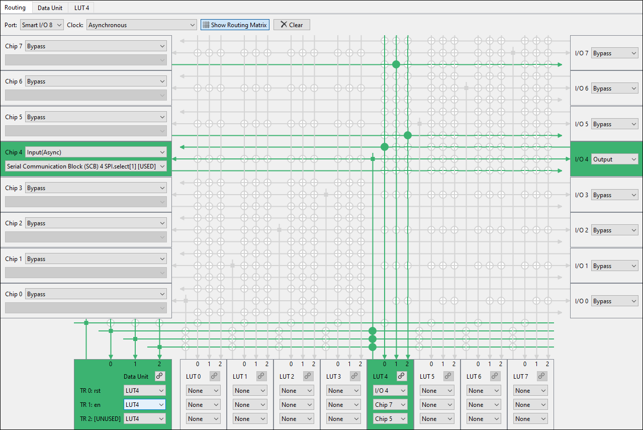
This tab contains the following parameters:
Port
Valid peripheral connections of a Smart I/O are port- and device-specific. This parameter allows selecting a port that supports Smart I/O.
Clock
Selects the clock source used to drive all sequential logic in the block. This clock is global within the Smart I/O and has differing constraints suited to different applications. Refer to the
Functional Description
section for more information.
Signal on I/O terminal 7…0
– Uses the selected I/O signal as the clock source. This signal may not be used in LUT inputs if used as the clock source.
Signal on Chip terminal 7…0
– Uses the selected Chip (peripheral or UDB) signal as the clock source. This signal may not be used in LUT inputs if used as the clock source. This clock can only be used during chip active and sleep modes.
Peripheral clock divider (Active)
– Divided clock from HFCLK. This clock is operational only in chip Active and Sleep modes. Sequential elements will be reset when entering Deep-Sleep or Hibernate mode and at POR.
Peripheral clock divider (Deep-Sleep)
– Divided clock from HFCLK. This clock is operational only in chip Deep Sleep modes. Sequential elements will be reset when entering Hibernate mode and at POR.
Peripheral clock divider (Hibernate)
– Divided clock from HFCLK. This clock is operational only in chip Hibernate modes. Sequential elements will be reset only at POR.
Clk_LF
– Low Frequency clock (either from ILO or WCO). This clock operates during chip Active, Sleep and Deep-sleep and allows the Smart I/O sequential logic to be clocked during those power modes.
Asynchronous
– If the Smart I/O is used purely for combinatorial logic, this option allows the block to conserve power by not using a clock. There are no constraints to power modes with this selection.
Show Routing Matrix
This button hides or displays the Smart I/O routing matrix. If the routing matrix is shown, you may click on the switches in the fabric to make input connections to the LUTs.
Clear
Click on this button to reset the routing matrix. All DU and LUT inputs will be cleared and the Chip and I/O terminal directions will become bypassed.
Chip configuration
There are eight
Chip
signals that can be configured. Each has two pull-down menus; one to select the direction of the signal and the other to select the connection.

Chip 7…0 direction
Defines the direction of the specified Chip terminal. Valid options include:
Bypass
– The line is bypassed and do not go through the Smart I/O routing fabric. That is, the Connection between the chip resource and the pin are directly connected.
Bypass
option frees this line and allows ModusToolbox™ to use this pin location for placing resources not meant to be used in the Smart I/O fabric.
Input (Sync/Async)
– Changes the direction of the terminal to be input type and allows connecting the matching peripheral/UDB signal to it. Input signals can be used as inputs to the LUTs. These can be either synchronized to the clock or remain asynchronous.
Output
– Changes the direction of the terminal to be output type and allows connecting the matching peripheral/UDB signal to it. Output signals can only be driven by the corresponding LUT outputs.
None
– The Chip terminal is consumed and cannot be used for connecting chip resources to it. This option is chosen automatically if the corresponding I/O terminal on the channel is specified as either
Input
or
Output
. You may use the terminal if the direction is set to Output or Input (only allowed if corresponding
I/O
is
Output
).
Chip 7…0 connection
When a
Port
is specified, these parameters allow each of the
Chip
terminals to connect to another peripheral on the chip.
I/O configuration
There are eight
I/O
signals that can be configured. Each has a pull-down menu to select the direction of the signal.

I/O 7…0 direction
Defines the direction of the specified I/O terminal. Valid options are:
Bypass
– The line is bypassed and do not go through the Smart I/O fabric. That is, the Connection between the chip resource and the pin are directly connected.
Bypass
option frees this line and allows ModusToolbox™ to use this pin location for placing resources not meant to be used in the Smart I/O fabric.
Input (Sync/Async)
– Changes the direction of the terminal to be input type and allows connecting an input I/O pin to it. Input signals can be used as inputs to the LUTs. These can be either synchronized to the clock (
Sync
) or remain asynchronous (
Async
).
Output
– Changes the direction of the terminal to be output type and allows connecting an output I/O pin to it. Output signals can only be driven by the corresponding LUT outputs.
None
– The I/O terminal is consumed and cannot be used for connecting a pin to it. This option is chosen automatically if the corresponding Chip terminal on the channel is specified as either
Input
or
Output
. You may use the terminal if the I/O direction is set to
Output
or
Input
(only allowed if corresponding
Chip
is
Output
).
Data Unit input configuration
The
Data Unit
configuration section contains three pull-down menus to select inputs. As you make various selections, the
Data Unit tab
becomes available for selection. You can also click the link icon to access the tab.

DU TR0, TR1, TR2
Defines the inputs for Data Unit triggers TR0, TR1 and TR2. The purpose of the triggers are dependent on the chosen Opcode as specified in the
Data Unit tab
. The triggers are active high.
Constant 0
– Default input selection. This effectively makes the trigger input to not perform any operation on the DU.
Constant 1
– Ties the trigger high, which activates and maintains the chosen DU operation.
DU
– Feeds back the single 1-bit DU output.
LUT 0…7
– Accepts any of the LUT outputs as an input.
LUT input configuration
There are eight
LUT
signals that can be configured. Each LUT configuration section contains three pull-down menus to select inputs from
Chip
,
I/O
, and
DUT
resources. As you make various selections, the corresponding
LUT tabs
becomes available for selection. You can also click the link icon to access the tab.

LUT 7…0, Input 0
Defines the input 0 of the specified LUT. The actual valid selection depends on the enabled/used resources and terminals in your design. The LUT input 0 may accept any LUT outputs as an input with the exception of LUT 0. Instead, it may accept the DU output as an input.
DU
– The 1-bit output from the DU.
LUT 1…7
– Accepts the outputs of LUT1 to LUT 7.
If using LUT 0…3, I/O / Chip 0…3 signals are allowed as potential inputs.
If using LUT 4…7, I/O / Chip 4…7 signals are allowed as potential inputs.
LUT 7…0, Input 1
Defines the input 1 of the specified LUT. The actual valid selection depends on the enabled/used resources and terminals in your design.
LUT 0…7
– Accepts the outputs of LUT0 to LUT 7.
If using LUT 0…3, I/O / Chip 0…3 signals are allowed as potential inputs.
If using LUT 4…7, I/O / Chip 4…7 signals are allowed as potential inputs.
LUT 7…0, Input 2
Defines the input 2 of the specified LUT. The actual valid selection depends on the enabled/used resources and terminals in your design.
LUT 0…7
– Accepts the outputs of LUT0 to LUT 7.
If using LUT 0…3, I/O / Chip 0…3 signals are allowed as potential inputs.
If using LUT 4…7, I/O / Chip 4…7 signals are allowed as potential inputs.
Data Unit tab
When the DU in the
Routing
tab is configured to accept an input other than a Constant 0, the corresponding
Data Unit
configuration tab will appear.
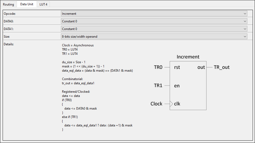
This tab contains the following parameters:
Opcode
Defines the Data Unit operation. Each opcode performs a unique function that can be controlled using the DU trigger inputs TR0, TR1 and TR2.
Note:
Not all trigger inputs are required for a chosen Opcode. Refer to the pseudo verilog code in the Details window and also to the Functional Description section for more information.
Increment
– Implements an 8-bit One-shot Up Counter. The DU output goes high when the internal DU working data register is equal to DU DATA1 value.
TR0 = reset signal that resets the working register to DU DATA0 value
TR1 = enable signal to start the increment operation
Decrement
– Implements an 8-bit One-shot Down Counter. The DU output goes high when the internal DU working data register is equal to 0.
TR0 = reset signal that resets the working register to DU DATA0 value
TR1 = enable signal to start the decrement operation
Increment and wrap
– Implements an 8-bit Up Counter that wraps when it reaches DU DATA1 value. The DU output is a single clock pulse when the internal DU working data register is equal to DU DATA1 value.
TR0 = reset signal that resets the working register to DU DATA0 value
TR1 = enable signal to start the increment operation
Decrement and wrap
– Implements an 8-bit Down Counter that wraps when it reaches 0. The DU output is a single clock pulse when the internal DU working data register is equal to 0.
TR0 = reset signal that resets the working register to DU DATA0 value
TR1 = enable signal to start the decrement operation
Increment/Decrement
– Implements an 8-bit Up/Down Counter. The DU output goes high when the internal DU working data register is equal to either DU DATA1 register or if it is equal to 0.
TR0 = reset signal that resets the working register to DU DATA0 value
TR1 = enable signal to start the increment operation
TR2 = enable signal to start the decrement operation
Increment/Decrement and wrap
– Implements an 8-bit Up/Down Counter that wraps when it reaches either DU DATA1 (count up) or when it reaches 0 (count down). The DU output goes high when the internal DU working data register is equal to either DU DATA1 register or if it is equal to 0.
TR0 = reset signal that resets the working register to DU DATA0 value
TR1 = enable signal to start the increment operation
TR2 = enable signal to start the decrement operation
Rotate Right
– Implements a right circular shift register. The DU output is the LSB of the working register, which also gets fed back to the MSB of the working register.
TR0 = load signal that loads the working register with DU DATA0 value
TR1 = enable signal to start the shift right and rotate operation
Shift Right
– Implements a right shift register. The DU output is the LSB of the working register.
TR0 = load signal that loads the working register with DU DATA0 value
TR1 = enable signal to start the shift right operation
TR2 = shift in value that gets inserted into the MSB of the working register
AND
,
OR
– Implements a bitwise AND operation on the DU working register and DU DATA1. The DU output is high if the result of the operation is true.
TR0 = load signal that loads the working register with DU DATA0 value
Shift right and Majority 3
– Implements a shift register with a majority 3 comparison. The DU output will go high if the contents of the working register is equal to 0x03, 0x05, 0x06 or 0x007.
TR0 = load signal that loads the working register with DU DATA0 value
TR1 = enable signal to start the shift right operation
TR2 = shift in value that gets inserted into the MSB of the working register
Shift right and Compare
– Implements a shift register with a match DU DATA1 value comparison. The DU output will go high if the contents of the working register is equal to DU DATA1.
TR0 = load signal that loads the working register with DU DATA0 value
TR1 = enable signal to start the shift right operation
TR2 = shift in value that gets inserted into the MSB of the working register
DATA0
Defines the DU DATA0 register source. This value is often used as the initial/reset value that is loaded into the DU working register when TR0 signal is high.
Constant 0
– Source is constant 0x00
Chip signal [7:0]
– Sourced from all 8 Chip terminals of the Smart I/O, allowing internal chip signals to be directly loaded into DATA0
I/O Signal [7:0]
– Sourced from all 8 I/O terminals of the Smart I/O, allowing external signals to be directly loaded into DATA0
DATA Register
– Sourced from the DU Register, which is accessible by the CPU
DATA1
Defines the DU DATA1 register source. This value is often used as the comparison value that gets applied to the DU working register.
Note:
DU DATA1 is not necessary for all Opcodes.
Constant 0
– Source is constant 0x00
Chip signal [7:0]
– Sourced from all 8 Chip terminals of the Smart I/O, allowing internal chip signals to be directly loaded into DATA1
I/O Signal [7:0]
– Sourced from all 8 I/O terminals of the Smart I/O, allowing external signals to be directly loaded into DATA1
DATA Register
– Sourced from the DU Register, which is accessible by the CPU
Register Value
Defines the 8-bit DU Reg value. This value is used as a source for DATA0 and/or DATA1.
Note:
DU Reg is available only if either DATA0 or DATA1 are configured to be sourced from it.
Size
Defines the bit size operation to be performed by the data unit. Valid range is from 1 to 8 bits.
LUT tabs
When a LUT in the
Routing
tab is configured to accept an input, the corresponding
LUT
configuration tab will appear.
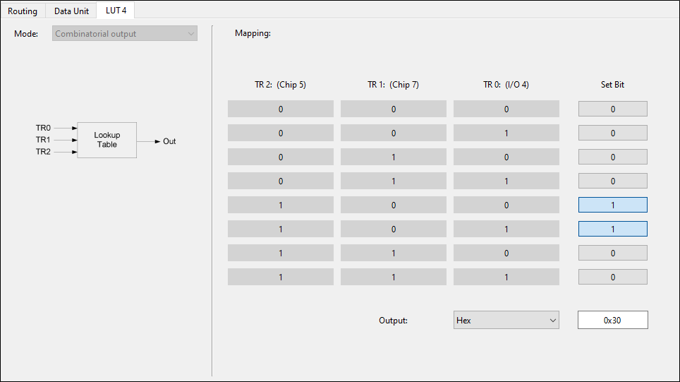
This tab contains the following parameters:
LUT 7…0 mode
The LUTs can be configured in one of four modes:
Combinatorial
– The LUT is purely combinatorial. The LUT output is the result of the LUT mapping truth table, and will only be delayed by the LUT combinatorial path.
TR2 gated, combinatorial output
– The LUT input 2 is registered. The other inputs are direct connects to the LUT. The LUT output is combinatorial. You may use the output to feed back into input 2.
Sequential (gated) output
– The inputs are direct connects to the LUT but the output is registered.
Asynchronous Set/Reset mode
– The inputs and the LUT truth table are used to control an asynchronous S/R flip-flop.
LUT 7…0 output mapping
Defines the look-up truth table of the 3-to-1 LUT. The state on the three inputs (input 0, 1 and 2) are translated to an output value according to this truth table.
Note:
If the LUT is used to operate on a single signal (for example, to invert a signal), then that signal must be connected to all 3 inputs of the LUT.
LUT 7…0 Notes
If visible, the
Notes
section allows you to document the interaction with the PSoC™ peripherals as you are setting up the logic for each of the LUTs. For example, a common use case might be to condition a signal before using it to trigger an internal peripheral. Having a comment about the logic setup provides a quick reference when reviewing the design at a later time.