AN221111 PSoC™ 6 MCU designing a custom secured system
About this document
Scope and purpose
This document teaches you what is required to create a secured system, from the boot process all the way to your application execution with PSoC™ 62/63 devices. The companion code example CE234992 PSoC™ 6 MCU: Security Application Template implements many of the topics described in this document.
Intended audience
This application note is intended for developers that want to learn more about the security features of the PSoC™ 62/63 family of devices.
More code examples? We heard you.
To access an ever-growing list of hundreds of PSoC™ code examples, please visit our code examples web page. You can also explore the video training library here.
Introduction
This application note teaches you about the security features of the Infineon PSoC™ 62/63 families and how to utilize these features to secure your application. Knowing this information will allow you to design a secure system that fits the needs of your application.
This is an advanced application note and assumes that you are familiar with the basic PSoC™ 6 MCU architecture described in the device datasheet and the technical reference manual (TRM).
This document will cover the following topics:
-
Assessing your security needs
-
Security Features of the PSoC™ 62/63
-
Understanding the PSoC™ 6 bootup sequence
-
What is a Chain of Trust (CoT) and do you need it?
-
What is and how to use a public/private key pair
-
Signing your application
This application note does not cover side channel attacks where an attacker tries to gain information from a microntroller by exploiting weaknesses in the device implementation, which includes timing, power-monitoring, electromagnetic attacks, and micro probing.
Use the code example CE234992 “PSoC6™ MCU: Security Application Template” as a companion document with this application note. Most code snippets in the application note are copied directly from CE234992. Also, CE234992 can be used as a template for a secured application. It supports the following features:
-
Secure boot
-
Bootloader (MCUboot)
-
Dual CPU (CM0+ and CM4) support
-
Real time RTOS (FreeRTOS)
-
Device firmware update (DFU)
-
1 M, 2 M, 512 K and 256 K PSoC™ 61/62/63 devices
There are two generations of PSoC™ 6 devices and they have some minor differences in the way they operate or how they are configured. The table below identifies the PSoC™ 6 families and which generation they belong. This document will refer to these parts as 1st and 2nd Generation PSoC™ 6 devices.
1st Generation PSoC™ devices | CY8C61x6, CY8C62x6, CY8C63x6 CY8C61x7, CY8C62x7, CY8C63x7 |
2nd Generation PSoC™ devices | CY8C61x4, CY8C62x4 CY8C61x5, CY8C62x5 CY8C61x8, CY8C62x8 CY8C61xA, CY8C62xA |
System security
Twenty-five years ago, few embedded system developers thought too much about security. Security meant that you did not release your source code to the public and you knew that few people would attempt to reverse engineer the binary code that was in your device. Also, the level of connectivity was almost non-existent, compared to today with the Internet of Things. Even the smallest electronic devices are wirelessly connected with either Wi-Fi or Bluetooth® LE. The other change is that most of the embedded devices on the market contain one of more Arm® processors and share a common SWD (Serial Wire Debugger) which makes it easy for a hacker to switch from one device to another without much of a learning curve.
At the start of any new project, security should be discussed and determine what needs to be protected. Usually the first thought is to protect the code and hardware from being hacked, but you should also consider any user data that may be collected or transmitted to the cloud or another location. It is not just that you are protecting code from being read but, protecting it from being modified or misused as well. The same goes for user data. Manipulating user data can be just as dangerous as reading the data. When evaluating what should be protected in your system, the list below is some of the items that should be considered. Not all the items in this list are required for every application, but you need to decide what is important.
-
Protect OEM IP (code/data/keys)
-
Protect end user data and keys
-
Confirm code integrity (CRC or hash)
-
Authenticate code origin (signing)
-
Authenticate firmware updates
-
Protect hardware from unauthorized usage
-
Isolate the two CPU’s memory space (dual core)
-
Protect data transmitted to and from the device
Protecting your firmware IP is probably the most obvious concern. If someone were to download and reverse engineer your code, they could more quickly get to market and pose direct competition. Although this is a valid threat, a security breach into your system could prove much more devastating to your product line than just added competition. If it was found that your device could be compromised, user data stolen, or taken control of, it could end the sales of the product overnight.
Most of the attacks usually come from outside the microcontroller, but there are attacks that can come from inside as well. Some attacks are accidental, for example, one CPU might crash due to a coding error and write data over the second CPUs stack or data area. Although this is not a malicious attack, the outcome can be just as serious.
When using two cores and code from multiple sources, without any protection applied, both CPUs have full access to the entire memory space. By isolating and protecting these CPUs from each other, you can guarantee that malicious or accidental failure does not cause system instability, failure, or misuse.
There are four main ways products can be hacked:
-
Direct access to the debug port. With the use of common debug tools and dongles, accessing or reprogramming firmware or examining internal data is easy. Most common CPUs are based on just a few architectures, so hacking or reverse engineering a product is easy if the device is left unsecured.
-
Direct connection to a communication port such as SPI, I2C, or a UART. Depending on the firmware, this connection may allow firmware to be read or updated with non-sanctioned software. If one person decodes the protocol and posts it on the internet, you can have many hackers gaining access.
-
Network connections such as Bluetooth®, Wi-Fi or ethernet. This has become the standard method of hacking because it does not require physical contact. The perpetrator can be out on the street or half way around the world via the internet. The firmware stacks to handle these interfaces are complex and difficult to fully test against all attacks.
-
Third-party code that’s installed in the device after it has been shipped. For example, the applications that you download into your smart phone. Malicious code in third-party applications can be dangerous because the code is already inside the device. This code must be kept inside a controlled environment with limited access to memory and system utilities.
Not all applications require the full gamut of security tools, you may not need to read all sections of this application note. Table 2 provides a few application examples and which sections of the Security features chapter you should consider reading.
| Example | Firmware updates | Intellectual property secure | Sections to read (Chapter 3) | Comment |
|---|---|---|---|---|
Simple toy #1 | No | No | NA | Device does not need to be secure. |
Simple toy #2 | No | Yes | Device lifecycle Debug ports | Device does not communicate with other devices or connect to the cloud. Disabling the debug ports is all that is required. |
Simple appliance | Yes | Yes | Device lifecycle Debug ports Authenticate CoT | Device is not connected to wireless devices. Code is updated with a dedicated link or device. Code requires authentication. |
Simple connected appliance | Yes | Yes | Device lifecycle Debug ports Authenticate CoT | This device may be connected wirelessly to cloud or other devices. Code updates need to be authenticated. |
Wi-Fi/Bluetooth® LE connected device | Yes | Yes | Device lifecycle Debug ports Authenticate CoT Protection units | Device is connected with a complex stack (Bluetooth® LE, Wi-Fi, etc.). The stacks should be protected/isolated. Also like the previous example, code should be authenticated. |
Security basics
A security plan is how you define access to your device. You can split this into two types, external and internal.
External access
By default, external access is only through the debug port unless the designer adds an additional communication port such as UART, I2C, SPI, Wi-Fi, Bluetooth® LE, and so on, which allows access to the memory. A bootloader can be used to update the firmware with your application using a communication interface of your choice. Unlike the debug ports, the developer can limit access to internal memory from the outside. It allows an alternate path to update the secured code and data but can be just as dangerous as the debug port if written incorrectly.
It is common and recommended that all debug ports are disabled, and firmware is updated only with a bootloader. How the data is transmitted to the device and whether it is encrypted or not is up to the designer. Listed below are four different secure system strategies for the external part of your security plan. Each of the pieces to implement these strategies are discussed in the Security features chapter.
-
Firmware updates with a hardware debugger: This is usually not thought of as a secure system, but if the hardware is installed such that a third party cannot get direct access, then it may be secure. Flash areas can be blocked from writing so that any internal hack could not change or replace the application. The device can be put in a SECURE lifecycle stage with the debug port open, which will force the firmware to be authenticated with a public key each time the device comes out of reset.
-
No access to debug port; bootloader for updates: The debug access ports are disabled so that after the initial programming, the only way to update the firmware is to provide a bootloader. The security level of the bootloader is determined by the implementation. The PSoC™ 6 family includes a Crypto block that can be used to generate the hash, encrypt, or decrypt to implement secured bootloader features. For systems that do not include an internal crypto block like in PSoC™ 6, Infineon OPTIGA™ embedded security products can provide a good alternative.
-
Lock down firmware; no updates: Debug access ports are disabled and there is no provision to allow for bootloading. This may be the most secure, but there is no way to perform bug fixes or add future enhancements.
-
Hybrid: A custom secure design that allows partial access to the memory via the debug port. This may fit your custom needs but will require more work and thought.
Internal access
The internal portion of your security plan is how the code and data are protected inside the device. Each application will be unique depending on how your CPUs are utilized, what the memory requirements are, and what is running on each CPU.
-
No protection: No protection or limits on the CPUs to access all data and code on the device. Because the code is all from the developer, it is assumed there is no malicious code. There also is no protection from one CPU firmware bug possibly corrupting the SRAM used by the other CPU.
-
Isolated CPUs: In this model, the two CPUs are totally isolated with perhaps one area of shared memory. Protection units are used to disallow any accidental reading/writing of data between CPUs. Communication between CPUs is achieved with shared memory or IPC hardware.
-
Secured CPU: This model uses the CM0+ CPU as the secured processor. In addition to being used for system calls, CM0+ will be used for all secure data and secure functions. Protection units are configured and owned by CM0+, so CM4 will not have access to secure data/code unless required by the system design. This is by far the most secured approach.
Basic definitions
Before continuing, you must understand some terms that will be used throughout this document. Many of these terms will be discussed in more detail in the following sections of this application note.
Chain of Trust (CoT) | Chain of Trust is established by validating the blocks of software starting from the root of trust located in the ROM. The root of trust begins with the Infineon code residing in the ROM that cannot be altered. |
Code signing | Process of calculating a hash of the code binary and encrypting the hash with a private key and appending this to the code binary. |
Dead access restrictions (DAR) | Determines what resources are accessible via the debug port when in DEAD mode. DEAD mode occurs if an error is found during the boot sequence. The DAR are stored in eFuse. |
Debug access port (DAP) | Interface between an external debugger/programmer and PSoC™ 6 MCU for programming and debugging. This allows connection to one of three access ports (AP), CM0_AP, CM4_AP, and System_AP (Sys_AP). The System_AP can access only the SRAM, flash, and MMIOs, not the CPU. |
Digest | The output of a cryptographic hash function is often called a message digest or digest. This digest is then encrypted with a private key to form a digital signature. |
Digital signature | Encrypting of the digest (hash of a data set). For example, the encrypted hash of the user application. |
Elliptic-curve cryptography (ECC) | ECC is an asymmetric encryption system that uses two keys. One key is private and should not be shared, and the other is public and can be read without loss of security. ECC is a more modern method than RSA and requires a smaller key than RSA for the same level of security. |
eFuse | One-time programmable (OTP) memory that by default is 0 and can be changed only from 0 to 1. eFuse bits may be programmed individually and cannot be erased. |
Factory hash | Calculated hash (SHA-256) of the system trim values and Flash boot. This hash is truncated to 128-bit (MSbs) and stored in the eFuse prior to leaving Infineon. This is used to validate that trim values and Flash boot (part of the boot sequence) have not been compromised. |
Flash boot | Part of the boot system that performs two basic tasks: Sets up the debug port based on the lifecycle stage. Validates the user application before executing it. Flash boot executes after ROM boot. |
Flash (User) | Flash memory that is used to store your application code. It is non-volatile by may be reprogrammed. |
Hash | A crypto algorithm that generates a repeatable but unique signature for a given block of data. This function is non-reversible. |
IP | Intellectual property. This can be both code and data stored in a device. |
Inter-process communication (IPC) | Inter-processor communication. Hardware used to facilitate communication between the two CPU cores. |
Lifecycle stage (LCS) | The LCS is the security mode in which the device is operating. To the user, it has only four stages of interest: NORMAL, SECURE, SECURE_WITH_DEBUG, and RMA. |
Memory protection unit (MPU) | The MPU is used to isolate memory sections from different bus masters. |
MMIO | Memory-mapped input/output, usually refers to registers that control the hardware I/O. |
Normal Access Restrictions (NAR) | Normal access restrictions determine what memory resources are accessible via the debug port when in NORMAL mode. The NAR is stored in SFlash. |
Protection context (PC) | The PC allows each bus master a security state level from 0 to 15. A bus master can be assigned a PC value that stays static or that is changed during application execution. PC provides a more precise way of applying memory restrictions. PC=0 is a special case which allows any bus master to have full access to the entire memory space including registers. The PC state works together with protection units. |
Protection units | Hardware blocks that are used to limit the bus master access to the memory (SRAM, ROM, flash) or hardware (peripheral) registers. They include MPU, PPU, and shared memory protection unit (SMPU). |
Peripheral protection unit (PPU) | PPUs are used to restrict access to a peripheral or set of peripherals to only one or a specific set of bus masters. |
Protection state | Three possible states: NORMAL, SECURE, and DEAD. Each state may be configured by the user. The NORMAL protection state configuration is stored in SFlash, but SECURE and DEAD state configurations are stored in the one-time programmable eFuse. |
Public-key cryptography (PKC) | Also known as asymmetrical cryptography. Public-key cryptography is an encryption technique that uses a paired public and private key (or asymmetric key) algorithm for secure data. It is used to secure a message or block of data. The private key is used to encrypt data and must be kept secured, and the public key is used to decrypt but can be disseminated widely. |
Public key | When using asymmetrical cryptography such as RSA or ECC, a public key is used to validate firmware that was signed by the private key. It can be shared, but it should be authenticated or secured so it cannot be modified. |
Private key | When using asymmetrical cryptography such as RSA or ECC, the private key is used to sign (encrypt the hash) of firmware after it is built but prior to being loaded into the device. It must be kept in a secure location, so it cannot be viewed or stolen. |
RMA | Return Merchandise Authorization |
ROM | Read-Only Memory is non-volatile and is programmed as part of the fabrication process and cannot be reprogrammed. |
ROM Boot | After a reset, the CM0+ starts executing code that has been programmed into ROM. This code cannot be altered. |
RSA-nnnn | An asymmetric encryption system that uses two keys. One key is private and should not be shared and the other is public and can be read without loss of security. The encryption/decryption is controlled by a key that is commonly 1024, 2048, or 4096 bits in length (RSA-1024, RSA-2048, or RSA-4096). |
Secure Access Restrictions (SAR) | Secure access restrictions determine what memory resources are accessible via the debug port when in SECURE mode. The SAR is stored in eFuse. |
Secure hash | Calculated hash (SHA-256) of the system trim values, Flash boot, TOCs, and user public key. This hash is generated during the transition to SECURE and stored in eFuse. This insures that the OEM’s public key has not be corrupted maliciously or accidentally. |
Security plan | The security plan is the set of rules that the designer imposes to determine what resources are protected from outside tampering or between the internal CPUs. |
Serial memory interface (SMIF) | A SPI (serial peripheral interface) communication interface to serial memory devices, including NOR flash, SRAM, and non-volatile SRAM. |
Supervisory Flash (SFlash) | Supervisor flash memory. This memory partition in flash contains several areas that include system trim values, Flash boot executable code, public key storage, etc. After the device transitions into a SECURE mode, it can no longer be modified. |
SHA-256 | SHA-256 is a common cryptographic hash algorithm used to create a signature for a block of data or code. This hash algorithm produces a 256-bit unique signature of the data no matter the size of the data block. |
Shared memory protection unit (SMPU) | SMPUs are used to allow access to a specific memory space (flash, SRAM, or registers) to only one or a specific set of bus masters. |
System calls | System calls are functions such as flash write commands that are executed by the Arm® Cortex® M0+ CPU (CM0+) from ROM. These system calls may be called from either the CM4 or CM0+ CPUs, or via the debug ports. |
Table of Contents1 | (TOC1) An area in SFlash that is used to store pointers to the trim values, Flash boot entry points, etc. It is used only by the boot code in the ROM and is not editable by the designer. |
Table of Contents2 | (TOC2) An area in SFlash of the PSoC™ 6 MCU that is used to store parameters and pointers to objects used for secure boot. Locations of two application pointers (Application1 and Application2) are stored here, but the second one is optional. The first pointer, Application1, must point to the first executable user code, which may be the bootloader or just the application. The table of contents also contains some boot parameters that are settable by the system designer. A duplicate of TOC2 is written in the adjacent page of flash for redundancy. This duplicate is called “RTOC2”. If TOC2 is found to be invalid for any reason, RTOC2 is evaluated. Both these structures are protected with a CRC, and are part of the Secure Hash. Definition of the TOC2 structure can be found in section 4.1. |
Security features
PSoC™ 6 MCUs has several security features that are used to build a custom secured system. In this chapter, each of these components will be described. The combination of these features can provide a secured system that meets most security requirements.
-
eFuse
-
Device lifecycle
-
Secured boot sequence
-
Chain of Trust (CoT)
-
Code signing
-
Protection units and protection context
-
Debug port configuration
The PSoC™ 62/63 family is a dual-core device with a CM0+ and a CM4 CPU. The CM0+ is usually considered the secured processor and is the one that performs all system calls and runs the secured boot sequence. The “main()” function in the user project enables CM4 only after CM0+ has run the boot process. The CM4 is usually considered the application processor because it can run faster and is more powerful than CM0+. The CM0+ is the logical choice to configure your secure elements, because it runs before CM4. This allows your application to have your secure configuration complete before enabling CM4.
It is also important to understand that in all but the simplest secure system, all these security features work together:
-
eFuse block: System hash values and security attributes are stored in the immutable efuse block.
-
Device lifecycle stage (LCS): The LCS dictates how the device boots up and which security attributes to enable, such as the SAR, NAR and DAR.
-
Chain of Trust: This dictates that the validation of the user application code is linked all the way back to the device ROM. The code verification is accomplished using the user’s public key stored in SFlash. A hash is calculated for the SFlash area and stored in eFuse. Any changes in the eFuse, public key, or user code will be detected and boot will fail.
-
Protection units: These protect or isolate the code and data from different bus masters. They are also used to secure the hardware such as flash and effuse programming. The user can also protect other hardware such as GPIOs or communications ports.
-
Debug port: The debug port is initially used for programming and debug of the user application, but should be disabled after the device is in SECURE lifecycle stage.
eFuse
eFuses are simple devices but an integral part of security for the PSoC™ 6 devices. There are 1024 eFuse bits which default to “0” and can only be programmed to a “1”. Once programmed, they cannot be erased back to “0” ever, not even by Infineon.
eFuse bits are stored in the programming file (intel hex) using the address range
0x9070_0000 to 0x9070_03FF. This range is virtual and
cannot be used for direct read or write operations. The eFuse library uses the offset
value to read 8 bits of eFuse data at a time.
Table 4 identifies the usage areas of interest in the eFuse block including the user area. Note that there is some difference in the eFuse usage between 1st generation and 2nd generation devices. Table 1 defines which family of parts belong to the 1st and 2nd generations devices
| Data | eFuse bit address in programming file | eFuse block byte offset (read) | Size | Notes |
|---|---|---|---|---|
Secure hash | 0x9070_00A0 | 0x14 | 16 bytes (128 fuses) | 128 bits of the MSbs of a 256-bit hash. Created when moving to SECURE mode. |
Secure hash zeros | 0x9070_0130 | 0x26 | 1 byte (8 fuses) | Number of zeros in the secure hash. This value is to ensure that the hash cannot be altered without being detected. |
DAR | 0x9070_0138 | 0x27 | 2 bytes (16 fuses) | Dead access restrictions |
SAR | 0x9070_0148 | 0x29 | 2 bytes (16 fuses) | Secure access restrictions |
Lifecycle | 0x9070_0158 | 0x2B | 1 Byte (8 fuses) | Lifecycle status |
Factory hash | 0x9070_0159 | 0x2C | 16 bytes (128 fuses) | 128 bits of the MSbs of the 256-bit hash. This is generated and stored before the device leaves the factory. |
Factory hash zeros | 0x9070_01E0 | 0x3C | 1 byte (8 fuses) | Number of zeros in the factory hash. Ensures that the hash cannot be altered without being detected. |
1st generation parts | ||||
User data | 0x9070_0200 | 0x40 | 64 bytes (512 fuses) | User eFuse area |
2nd generation parts | ||||
Asset hash | 0x9070_0200 | 0x40 | 16 bytes (128 fuses) | Similar to the factory hash, but it does not include trim values so it will be the same for all parts with the same silicon and firmware version. (This is generated and written to eFuse automatically) |
Asset hash zeros | 0x9070_0280 | 0x50 | 1 byte (8 fuses) | Number of zeros in the asset hash. Ensures that the hash cannot be altered without being detected. (This is calculated and written automatically) |
User data | 0x9070_0281 | 0x51 | 47 bytes (376 fuses) | User eFuse area |
Device lifecycle
The device lifecycle is a key aspect of the PSoC™ 6 MCU’s security. Lifecycle stages follow a strict irreversible progression
dictated by programming eFuses bits (changing a fuse’s value from ‘0’ to ‘1’). This system
is used to protect the internal device data and code at the level required by the customer.
Lifecycle stages are governed by the LIFECYCLE_STAGE
eFuses and can only be advanced to the next lifecycle state as shown in Figure 1. For example, once in the SECURE
lifecycle stage, the device can never return to the NORMAL or VIRGIN state.
Figure 1. Device lifecycle

VIRGIN
This is the initial lifecycle stage of the device when manufactured. During this stage, trim values and Flash boot are written into SFlash. Parts in this stage never leave the factory. Once all factory tests are passed and the factory hash is written, the device will be transitioned to the NORMAL lifecycle stage.
NORMAL
This is the lifecycle stage in which the parts are sent to customers. By default, users have full debug access and may program all user flash including certain areas in SFlash such as user SFlash, TOC2, and public key. To allow the OEM to check the data integrity of trims, Flash boot, and other objects from the factory, a hash (SHA-256 truncated to 128 bits) of these objects is stored in eFuse, called the “factory hash”. The factory hash is not verified during boot, but should be verified before moving to the SECURE lifecycle stage.
Normal access restrictions (NAR)
Access restrictions to the debug ports may be modified in the NORMAL lifecycle
state. Normal access restrictions (NAR) are located in SFlash
0x1600_1A00 and use the same format as the SARs in
eFuse. (See section Appendix C - Debug port access settings for NAR, SAR,
and DAR formats) Once set, they can be changed to be more restrictive, but not less, by
the flash write system call.
Note that the NAR settings are not considered secure because a user could alter the NAR by writing a custom flash write function instead of using the flash write system call. The system calls that write the flash memory will not allow erasing the bits in the NAR SFlash area.
Using NAR to secure a device
If you are considering using NAR to secure a device, you should set up the protection context registers and move all bus masters (CM0+ and CM4) to a protection context other than 0. This will disallow any direct access to the flash programming registers, other than the system call infrastructure that will not allow reducing the security of the normal access restrictions. This should be done preferably by CM0+ at the beginning of the CM0+ application (or bootloader) before running any user code in CM0+ or enabling CM4. This will effectively lock out any access to the registers required to program internal flash memory and force you to use flash write system calls to the program flash.
If you set the NAR to disable the debug ports and change the protection context to PC ≠ 0, you can protect access to your internal code and block anyone from accessing the code or debugging. This can be an attractive option for some applications. If you plan on upgrading your code in the future and have disabled the debug port, you will need a bootloader and a way to transfer the new code to the device other than the debug port before setting the NAR bits. One advantage of using NAR to lock out debug is that you can easily program the bits during runtime and it does not require the 2.5 volts connected to the VDDIO0 pin. One reason for programming the NAR values during runtime is that you could use your project application to disable the debug ports right before shipping the product after the device has been fully tested.
By default, in the NORMAL lifecycle stage, the user application code is not validated. There is an option to force your code to be validated with the public key while in NORMAL mode. This is a good way to validate that you have everything set up correctly before you advance to SECURE mode, because it boots the same way. If you move to the SECURE lifecycle stage and do not have the public key stored correctly or did not write the TOC2 properly, you can lock yourself out of the part and essentially “brick” the device so it is not usable, and there is no way to fix it. By using the NORMAL validation feature, you can continue to make changes until you have everything set up properly, and then you can feel more confident about advancing to the SECURE lifecycle stage. To force validation in the NORMAL LCS, you must populate the TOC2 structure and add the RSA public key, just as you would in the SECURE LCS. More details of the TOC2 structure are defined later in the application note.
SECURE
This is the lifecycle stage of a secured device. Before the transition to the SECURE lifecycle stage, the following tasks must be completed properly. Failure to do so could leave you with an inoperable device. The first five steps may occur in any order, but step six must be the last step. More information on performing these steps is provided later in this document.
-
Use the factory hash to verify that the device has not been tampered with since it left Infineon. The device programmer performs this check during the transition to the SECURE lifecycle stage. (See #6 below).
-
Fill in TOC2 including the CRC at the end (cymcuelftool which is included in the ModusToolbox™ install is used to fill in the CRC).
-
Write the public key into SFlash (See Appendix B - Creating crypto key pairs).
-
Set the SAR and DAR in the eFuse. Once in SECURE lifecycle stage, the access restrictions cannot be altered (See section Appendix C - Debug port access settings for NAR, SAR, and DAR formats).
-
Program an application into the user flash. Depending on the SARs, a bootloader may be required to update the code in the future.
-
Transition to the SECURE lifecycle stage by setting the SECURE Lifecycle stage bit. (The CYPRESS™ Programmer tool performs eFuse programming, but the user sets the values in his code.)
In the SECURE lifecycle stage, the protection state is set to SECURE and the SAR are deployed. A secured device will boot only when the authentication of its Flash boot and application code succeeds.
After an MCU is in the SECURE lifecycle stage, there is no going back. The debug ports may be disabled depending on your preferences, which means that there is no way to reprogram or erase the device with a hardware programmer/debugger. The only way to update the firmware at this point is to provide a bootloader as part of device firmware and provide a way to invoke it.
Code should be tested in NORMAL or SECURE_WITH_DEBUG
lifecycle stages before the move to the SECURE lifecycle stage. This is to prevent a
configuration error that could cause the part to be no longer accessible for device
programming and therefore unusable.
SECURE WITH DEBUG
This is the same as the SECURE lifecycle stage, except with NAR applied to
enable debugging. When in the SECURE_WITH_DEBUG lifecycle stage, the
access restrictions are taken from the NAR located in SFlash. Parts put in this stage
cannot be changed back to either SECURE or NORMAL stage; they are most likely discarded or
destroyed after testing. Devices should not be shipped in this stage because they are not
secure. It is not recommended to use this lifecycle stage during development; instead, use
the NORMAL lifecycle stage with the Validate App bits set in TOC2. Only use this Lifecycle
stage if you find that your device is not booting correctly in SECURE and you need to debug
the problem.
RMA
The RMA lifecycle stage is a mechanism to allow customers to return parts that are in the SECURE lifecycle stage back to Infineon to evaluate if a defect in the device is suspected. When in RMA mode, the debug ports will be open to allow Infineon to access all hardware and memory. Before switching the device to RMA, you should erase all proprietary and sensitive data and code in the device by means such as updating the firmware (with your bootloader).
See Appendix D - Transition to RMA for more details.
Protection state
Protection state and Lifecycle stage are the same unless there is an error during the boot process or the device is in the RMA Lifecycle. If there is an error during boot, the device will be moved to the “DEAD” protection state. Access to the debug ports in the DEAD protection state is defined by the Dead Access Restrictions (DAR).
Figure 2. Protection state transitions

CM0+ boot sequence
Only the CM0+ CPU is started after a reset. It is up to the OEM’s CM0+ code to enable the CM4 after the boot sequence, if the default CM0+ startup code is not used. The default CM0+ is a binary that is provided, if the user doesn’t need to use the CM0+. It is not recommended to use for a secure system. The boot sequence differs depending on which lifecycle stage the device is in. As expected, the SECURE lifecycle stage is the only boot sequence that maintains a Chain of Trust (CoT). Figure 3 shows the different paths of the four basic boot sequences.
-
NORMAL (no validation, no code security)
-
NORMAL with Validate (no code security)
-
SECURE_WITH_DEBUG (debug only, not intended for final product)
-
SECURE
Figure 3. PSoC™ 6 CM0+ boot sequence

NORMAL lifecycle boot
After reset and initial hardware configuration, Flash Boot (pre-programmed
into SFalsh) configures the DAP port with the NARs stored in the SFlash. The GPIOs used for
the debug interface are configured to interface with the debugger if any of the three debug
access ports are enabled (CM0+, CM4, System). By default, it is assumed that the user code
starts at 0x1000_0000 (beginning of user flash) and the first two vectors
are the stack pointer and the reset vector. These values are checked to verify that they
contain values that are in the available SRAM and flash respectively. If these values are
outside of these memory ranges, CM0+ will jump to DEAD mode and remain in an infinite loop,
and no (user) code will be executed.
SECURE lifecycle boot
When in the SECURE lifecycle stage, the following occur:
-
CM0+ validates the SFlash by calculating a hash of the trim values, Flash boot code, user public key, etc.
-
CM0+ compares this hash with the precalculated secure hash stored in the eFuse that was generated when the part was advanced from NORMAL to SECURE lifecycle stage by the OEM.
- The calculated SHA-256 hash (256 bits) is truncated to its most significant 128 bits which is the same as the stored hash in the eFuse.
-
If the calculated hash matches what is stored in the eFuse, the trim (calibration) values from the SFlash are used to configure the hardware for optimal operation.
-
CM0+ executes Flash boot (in the SFlash) and validates the Table of Contents2 (TOC2). The TOC2 contains information about the location of public key, start of user code, application format, user configuration options, etc. It also contains a 16-bit CRC for validation. One of the following occurs:
- If either the secure hash or TOC2 validation fails, CM0+ moves to DEAD protection state and remains in a continuous loop until the device is reset. This guaranties that only verified code will be executed, and no user code will be executed if there is a possibility that the device has been compromised.
- If the secure hash and TOC2 are validated, the debug access ports are configured to the values stored in the SARs bytes in the eFuse. The GPIO pins used for the debug port on the device are left in their default tristate mode and will not communicate to the debugger or programmer in this state, even if the SAR defines all ports to be open. The 1 M/512 K/256 K flash parts provide an option in the TOC2 to automatically configure the debug GPIO for debug operation. This allows you the flexibility to configure the secure hardware before the debug ports allow a connection. Your application can control the access dynamically if need be. Example code to enable the debug port is presented later in this document.
Note: The SAR bytes, public key, and TOC2 are written into the device prior to moving from NORMAL to SECURE lifecycle stage. Once in the SECURE lifecycle stage, these values cannot be modified.
-
The system has now been fully validated and the debug modes have been configured to the designer’s requirements. A header prefix (see section 4.2) was added to the user code that contains information such as number of CPUs (2 for PSoC™ 62/63) and the starting location for each CPU’s application code. Flash boot checks this header to determine the location where the user CM0+ code starts.
-
CM0+ jumps to the CM0+ user project.
The CM0+ user code that is first executed after Flash boot does not have to be the main application. It could in fact be a bootloader that manages updates for either CM4 or both CM0+ and CM4. Also, this may be a good place to implement your application-level security by programming protection units and the protection context. See Appendix E - Protection unit configuration for more details.
SECURE_WITH_DEBUG lifecycle stage
This lifecycle stage operates just as the SECURE lifecycle stage, except that it uses NARs so
that you can debug your device before moving to SECURE mode. Once you have moved to
SECURE_WITH_DEBUG mode, you CANNOT move back to NORMAL or to SECURE
lifecycle stage. Devices in this stage should never be shipped to the end customer.
NORMAL lifecycle stage with validate is a much better step to validate your key
generation and code signing. In SECURE_WITH_DEBUG, you can change your
application, but not SFlash which includes the private key and TOC2.
NORMAL lifecycle with validate
This is the NORMAL lifecycle stage with the option to validate the first code. It operates just as the SECURE lifecycle stage, but skips the secure hash validation, uses NAR instead of SAR, and configures the debug GPIOs for communication with the debug hardware before executing the user code.
This lifecycle stage is useful to verify that your key generation and code signing process is working properly. If you find a problem, it is easy to debug, and you can erase the entire device and start over if a problem is found. Make sure that you have not set the NAR to be too restrictive or enabled it at all so you can debug the problem. Once your key generation and code signing are validated, you are much less likely to have problems switching to the SECURE lifecycle stage. To enable code validation, you must create a valid TOC2 and set the appropriate bits in the Flash boot parameters. (See section 4.1 for details of TOC2.)
Debug boot errors
If there is an error during the boot sequence in NORMAL or SECURE lifecycle stage, the device will enter the DEAD state in which CM0+ stays in an endless loop. If the device was in the SECURE lifecycle stage, the device will change the protection context to PC=2. If in the NORMAL lifecycle stage, the PC value remains at PC=0.
Whether you can debug the device or not depends on your settings to access in the DEAD state. During debugging, you should leave full access to the debug ports. To determine what caused the boot sequence to fail and enter the DEAD state, read the value of IPC (#2) data register. An error code with the failure ID will be written into that register. See Appendix E - Protection unit configuration for boot sequence error table.
Chain of Trust (CoT)
At the beginning of the Chain of Trust, must be immutable code that cannot be altered. This first immutable code is referred to as the “Root of Trust” (RoT). The initial ROM code validates the Flash Boot code in SFlash to verify that it hasn’t been modified, prior to any code execution in SFlash.
Flash boot, trim constants, and the Table of Contents1 (TOC1) are located in SFlash (Supervisory Flash) and are restricted from being reprogrammed in either NORMAL or SECURE lifecycle stages.
The SFlash area is validated with a
Factory_HASH value stored in the eFuse. The
Factory_HASH code is not used during the boot sequence in
NORMAL or SECURE lifecycle stages, but is used to validate the part before moving to the
SECURE lifecycle stage. This ensures that the Flash boot code, trim values, and the TOC1
has not been tampered with after the MCU has left Infineon. If the
Factory_HASH has been corrupted, Infineon should be
contacted immediately. See Appendix F - Debug codes for failed boot sequences.
After the transition from NORMAL to SECURE lifecycle stage, all blocks in the SFlash,
including the public key area and the TOC2, are validated with the
Secure_HASH each time the device boots. This secure hash is stored in the
eFuse and cannot be changed without detection. If an error is found while validating the
SFlash, the device will abort the boot sequence and enter a DEAD state. Figure 4 shows the CoT from the perspective of data and
code validation.
Figure 4. Basic chain of trust

At this point, the entire SFlash is now trusted because its validation is based on the memory (eFuse) that cannot be modified without detection during SFlash validation in the ROM.
The (OEM) public key, which is locked into the SFlash, is secure and cannot be changed without being detected as well. It is used by Flash boot to validate the next step in the boot process. Flash boot validates the code in the user application block, which includes a digital signature at the end of the code block. Flash boot uses the SHA-256 hash function to calculate the digest of the user application. The digital signature attached to the user application is encrypted using a private key that is associated with the public key stored in the SFlash. The encrypted hash uses RSA 2048-bit encryption.
The calculated and the stored digest (decrypted digital signature) are then checked to see whether they match. If they match, the user application has been verified.
Code signing and verification
In the Chain of Trust (CoT) section, code verification was mentioned but with not much detail. In this section, we will dive into the process of signing a block of code so that it can be verified during runtime. Infineon supports the signing of application code using the CyMCUElfTool which is downloaded with ModusToolbox™ software.
The encryption method used is PKC (public key cryptography) that has a private and public key pair. You must ensure that the private key is kept in a secure location, so that it never gets into the public domain. If the private key is exposed, it will endanger your system’s security. Companies must create a method in which very limited access to the private key is allowed.
The public key, on the other hand, can be viewed by anyone. The only requirement is that the public key must be validated or locked in such a way that it cannot be changed, or so that any modification to the public key can be detected. In this example, the public key is stored in the SFlash and verified with the Secure_HASH as defined in the Chain of Trust (CoT) section. These private and public keys can be generated with common encryption libraries such as OpenSSL.
Do the following to transition a PSoC™ 62/63 device to the SECURE lifecycle stage and use code signing:
-
Fill in TOC2 and add the 16-bit CRC at the end of TOC2 (SFlash).
-
Fill in the RSA-2048 public key (SFlash).
-
Use standard CYPRESS™ application format (user flash) at the beginning of the application (See section 4.2 for definition).
-
Sign your application bundle and place the 256-byte (2048 bits) digital signature at the end of the code (user flash).
-
Enable NORMAL lifecycle code verification or move to SECURE lifecycle stage.
It is HIGHLY recommended to test the code verification in the NORMAL lifecycle stage before switching to the SECURE lifecycle stage. In the NORMAL lifecycle stage, if something is incorrect with the code signing process, you can reprogram the TOC2, public key, and update your application. Once you switch to the SECURE lifecycle stage, you cannot alter the TOC2 or update the public key. You may not be able to change your application with the programmer if you closed your debug ports and your bootloader is not yet implemented.
For more information on generating and using the private and public keys, see Appendix A - Code example of a security application template.
Code signing
To verify the user application, a digital signature is created and appended to the end of the code during build time. The code itself is not encrypted but the digital signature is the encrypted digest. The digital signature is generated by encrypting the digest with the RSA-2048-bit algorithm. The digest is generated by running the user application binary through a SHA-256 hash function. This type of code signing is used for both RSA and ECDSA algorithms, but PSoC™ 62/63 Flash boot code only supports RSA-2048. This method guarantees that a third-party without access to the OEM’s private key cannot properly sign the application code (see Figure 5Figure 5).
Figure 5. Generation of digital signature

Code verification
A secured system must be able to verify that its application code was indeed generated from a known source and detect if it has been modified by a third-party or corrupted. If the verification fails, the execution must take a known path to a safe state.
Parts of code validation
Verification requires three parts: application code, digital signature, and key pair (public and private). The application code and digital signature come as a pair; the public key is stored in the device such that it cannot be changed, without detection.
-
Application code: This includes both executable code and constants that makes up the firmware in an embedded system. This code usually resides in the flash memory that can be modified at one time or another. Therefore, you must be able to determine whether this code is from a known source (OEM) and has not been corrupted either by accident or by a malicious event.
-
Digital signature: A digital signature is the encrypted digest (hash) of the application code generated at the OEM. The digest of the application code is encrypted by the private key to generate the digital signature. The hash algorithm used in this case is SHA-256. The digital signature is then used to verify that the application before being executed.
-
Key pair: This asymmetric key pair contains both the private and public keys. In the system described in this application note, the public key is stored on the device and the private key is secured by the OEM. The public key must be secured in one of two ways (the second option is the most likely one for an embedded system):
- A method to verify the source of the key. This can be accomplished with some type of communication with a known source or server. This is not practical for devices that cannot easily communicate with a known server when required.
- Have the key protected such that it cannot be changed, or that you can determine if it has been modified. In the PSoC™ 6 devices, a hash is calculated from the areas containing the public key, Flash boot code, and trim values. This hash is then stored in one-time programmable eFuse and referred to as Secure_HASH. The hash is verified before the public keys is used.
Code verification used by PSoC 62/63 MCUs
The device bootup code “Flash boot” uses RSA to verify the first user code. The application binary code block (application bundle) includes a digital signature that is created during the build time. To verify the application code, a hash function (SHA-256) is calculated across the binary code block. Next, the digital signature is decrypted using the stored public key to reveal the original digest generated when the application was generated at the OEM location. The calculated digest and the decrypted digest (from digital signature) are compared to verify they are equal. If they are an exact match, the code is verified (see Figure 6).
ECDSA is another common algorithm used to verify application code. It is similar to RSA, but instead of decrypting the digital signature and comparing it to the calculated hash, the calculated digest, digital signature, and ECDSA public key are used to generate a pass or fail. This is a common method used by MCUboot to verify the application code. Figure 6 shows the comparison between RSA and ECDSA.
Figure 6. Application verification

Protection units
This section provides a brief description of how the protection units work and how to use them. For a more detailed description of protection units, read the “Protection Units” chapter in the PSoC™ 6 MCU Architecture TRM (Technical Reference Manual)for your device.
PSoC™ 6 has several bus masters that all share a single bus that interconnects the flash, SRAM, ROM, GPIOs, and peripheral control registers. The bus masters include the two CPUs (CM0+ and CM4), DMA controllers (Data Wire), crypto unit, and the test controller. Bus arbitration hardware keeps the bus masters from bumping into each other, but the protection units keep them from reading and writing into each other’s memory space.
Protection units can be programmed to allow only specific CPUs and other bus masters to access only predefined memory segments and peripherals. If a bus master attempts to use a section of memory not allowed by the protection unit, a bus fault will occur. Because the two CPUs (CM4 and CM0+) share the same memory space in the PSoC™ 6 MCUs, the protection units guarantee that one CPU cannot affect the memory or peripherals allocated to the other if needed. Not all memory or peripherals must be allocated to just one CPU; by default, the entire memory space is shared between the two CPUs and sections can remain that way if desired.
Protection units can also be used to isolate memory for different tasks that run concurrently in an RTOS. Different sections of a boot process may also be another example of securing sections of memory. For example, you may want your bootloader to have access to write to the flash in the user application area, but deny the user application from overwriting writing code that is executing. Protection units can be configured to do just that. Figure 7 shows how the different protection units (SMPU, MPU, PPU) are connected relative to the bus masters, peripherals and system bus (AHB).
Figure 7. Protection units with respect to the overall system

PSoC™ 6 has four types protections units:
-
SMPU – Shared memory protection units
-
MPU (Arm®) – Memory protection unit that are part of the CPU IP
-
MPU (Infineon) – Memory protection unit for test controller and crypto block
-
PPU – Peripheral protection unit (fixed and programmable)
SMPUs
The SMPUs are capable of protecting any section of the bus memory space, but they are meant to be used for segments of the ROM, SFlash, user flash, and SRAM. The CPUs (CM0+ and CM4) each contain an Arm® MPU that is part of the Arm® IP. The Arm® MPUs do not support protection context (will discuss this later), secure, or privileged modes. but they are primarily meant to be used in conjunction with an RTOS or other operating systems.
Two Infineon MPUs are used in the crypto block and the test controller (debug interface). For more information on these MPUs, see the Technical Reference Manual (TRM) for the device you are using.
PPUs
There are two different types of PPUs: fixed and programmable. Fixed PPUs are assigned a specific block of registers, usually for a single IP block such as a TCPWM, SCB, or SAR ADC. The address and region size are fixed and cannot be changed.
Programmable PPUs are similar to the SMPUs in that they can protect any region of peripheral device address space. They are meant to protect registers in a specific block that are not covered by the resolution of the fixed PPUs.
Protection unit configuration
Protection units have several parameters, besides just address and range. The following is a list of attributes that must be met when evaluating if the memory access is permitted by a bus master.
| Parameter | Description |
|---|---|
Address | Where the region starts. It must be aligned to the region size. |
Region size | Size of the region which is a power of 2 from 256 bytes to 4 GB. |
Sub regions | Disables any of 8 equal spaced regions. If Region size is 256, each sub region would be 32 bytes, each which can be disabled. |
User permission | Read/Write/execute for user level access. |
Privilege permission | Read/Write/Execute permission for CPU privilege mode. |
Secure | This bit is not directly associated with the NORMAL/SECURE lifecycle stage; it can be set for a bus master. You can use this bit to designate one of the bus masters as the “secure” processor, most likely the CM0+. This bit adds one more level of designation. For example, you could have two bus masters (CM0+ and CM4) both set to protection context equal 1, but only the designated secure bus master may have access to a region designated by a protection unit. |
PcMatch | This bit is valid only if two or more of the protection structures match the same address range that the bus master is attempting to address. If two or more protection structures match the bus master’s address request, the protection system will evaluate these structures from highest index (15) to lowest index (0). It will continue to evaluate these structures until if finds PC_MATCH = 0, at this point it will complete the evaluation of the present structure and not evaluate any further structures, even if the address or PC values match the request. If the present protection structures PC_MATCH = 1, it will continue to the next structure that has a valid address range. |
PcMask | Bitmap of what PC value may access memory region defined by this protection unit. |
All the protection units, except for the MPUs that are part of the Arm® CPUs, have a master protection structure associated with it. The master protects the PPU (slave) from being altered by any bus master that should not have access. In a sense, the master assigns an owner which is the protection context. See the next section for more information.
Although the two CPUs share the same bus, they run totally independent code. The code running in the two CPUs can even be written by two different companies, depending on how you structure your device. For example, the system calls in the PSoC™ 6 are written by Infineon, but the rest of the code will be written by the customer.
The bootup ROM enables protection units to protect the stack area and the registers that control writes to the flash and eFuse. This is important for the following reasons:
-
Prevent unintended modifications to the flash by the code in SECURE mode.
-
Protecting the flash control hardware forces the user to use systems calls to write to the flash which is guaranteed to optimize lifecycles with maximum retention.
-
Protected system calls adhere to the SMPU settings to determine who has permissions to change the flash in SECURE and NORMAL modes.
A common configuration for a secure system is to have CM0+ be the secure processor and CM4 be the main (non-secure) application processor. The two CPUs should operate independently of each other with only a controlled interface between them.
Using protection units, the memory spaces can be totally isolated from each other although they share the same memory bus. Peripherals and GPIOs, such as flash control, can be reserved by one CPU so it cannot be accessed by the other CPU. The controlled interface between the two CPUs as mentioned before can be the shared SRAM or in the case of system calls, a combination of shared SRAM and the IPC interface.
Bus masters
In PSoC™ 6 MCUs, a bus master is any block that can directly access the SRAM or flash without the aid of another bus master. There are at least six bus masters in the PSoC™ 6 MCUs, and maybe more in future devices. In this document, a mention of bus master includes the CM0+ and CM4 processors. Table 6 shows the bus masters and important configuration registers.
| Master # | Bus master | Master Protection Context Control register | Master Control register |
|---|---|---|---|
0 | CM0+ processor | PROT_SMPU_MS0_CTL | PROT_MPU0_MS_CTL |
1 | Crypto block | PROT_SMPU_MS1_CTL | PROT_MPU1_MS_CTL |
2 | DataWire 0 (DMA) | PROT_SMPU_MS2_CTL | Inherits settings from the CPU |
3 | DataWire 1 (DMA) | PROT_SMPU_MS3_CTL | Inherits settings from the CPU |
14 | CM4 processor | PROT_SMPU_MS14_CTL | PROT_MPU14_MS_CTL |
15 | Test controller | PROT_SMPU_MS15_CTL | PROT_MPU15_MS_CTL |
The Master Protection Context Control registers (PROT_SMPU_MSx_CTL) are key to making protection units function. They are used to configure each bus master with the appropriate attributes that the protection units use to determine access. The protection unit library contains the Cy_Port_ConfigBusMaster() function that can be used to configure these registers.
The Master Control register for each bus master controls the active protection context. The DataWire blocks do not have an associated register because they inherit their attributes from the CPU. The protection unit library (PROT) includes the Cy_Prot_SetActivePC() function to set the active protection context for the bus master. This function will only allow you to set a legal protection context for the device. Each device has a mask register that determines which PC (protection context) value can be assigned for that bus master. Documentation for all ModusToolbox™ (PDL) libraries may be found at PSoC™ 6 Peripheral Driver Library.
Protection contexts (PC)
Understanding how a protection context (PC) works is mandatory to configure the protection units. A protection context is similar to groups in a computer system while the bus masters are users in those groups. Each bus master (user) can belong to a subset of all possible PC values (groups), but can only be assigned one PC value at a time. PSoC™ 6 family devices support PC values of 0 through 7.
A bus master has a mask of what PC values it can be assigned, and the current PC value. At any time, the bus master can change its current PC value to one enabled in the mask, not to a PC value not in the mask. If a bus master’s PC mask enables PC values of 1, 2, and 3, and an attempt is made to change the PC value to PC=4, an error will occur and the PC value will not be changed. Without this feature, any bus master could just change its PC to any value.
A PC value of 0 is a special case. If a bus master has a PC=0, it may access any memory location without causing a page fault no matter how the protection units are configured. Think of it as super user mode. By default, all bus masters are set to PC=0 after reset. After all protection units are configured, all bus masters should be changed to a PC value other than 0 to make sure that the protection/security configuration cannot be altered.
Protection units are not assigned to bus masters, but instead you select which protection contexts are valid to access the region specified by the protection unit. Each protection unit has a PC mask that determines which PC values are accepted. During configuration, determine which PC values should have access to the region specified by the protection unit.
For example, if an SMPU was set up with a PC mask that allowed PC values of 4 and 5, bus masters with a PC value 4 or 5 that met all other criteria could access the region specified by the SMPU. A bus master with a PC=1 cannot access the region specified by this SMPU no matter it met all other criteria.
One or all bus masters can share the same protection context, or they may all be different. For example, sharing the SRAM with everyone but blocking any CPU from executing the code in the SRAM. A bus master with a PC=0, always has full read/write/execute to the entire memory space no matter the configuration of any protection units.
Although a bus master PC mask may allow several PC values, the currently selected PC value is the only one that matters when accessing a protected memory area. For example, CM4 (bus master) had a PC mask that allowed PC values 1, 2, and 3 and had a current PC value of 3. If it attempted to access a region protected by an SMPU that only allowed 1 or 2, the access would fail and cause a hard fault because the bus master’s current value was not 1 or 2. If CM4 had changed its protection context to 1 or 2 before accessing the region, the operation would work without error.
CM0+ is the only bus master that can switch back to PC=0. The system calls revert CM0+ back to PC=0 each time the system call ISR is executed. It does this by setting up CPUSS_CM0_PC0_HANDLER with the address of the system call ISR. When one of the three IPC channels (0, 1, or 2) causes an NMI (non-maskable interrupt) interrupt, CM0+ is automatically switched to PC=0, where it will execute the system call and then revert to the original PC value upon return of the of the interrupt. 1st generation parts can do this just for PC=0, but 2nd generation parts can be configured to automatically switch to PC values 1, 2, and 3 with an ISR.
See register description in the respective TRMs for CPUSS_CM0_PC1_HANDLER, CPUSS_CM0_PC2_HANDLER, and CPUSS_CM0_PC3_HANDLER.
SMPU/PPU master
Protection units are divided up into a slave and a master. The slave defines the memory or register space, protection parameters, and what PC values have access. The master protects the slave structure from accidental or intentional modification of the slave structure. There is always one master for each slave protection unit structure and therefore has a fixed address and region area that is only readable. After all slave structures are configured, it is best to own all masters by a single PC value, such as PC=0. This way after the bus masters have all be changed to PC ≠ 0, the system protection unit configuration is fixed.
Figure 8. Protection unit slave/master

Debug port configuration
See Appendix C - Debug port access settings for register and bit level definitions.
Debug port architecture
The physical interface to the debug port is the same as many other Arm®-based devices. It consists of either 3-pins for SWD, serial wire debugger (SWDCLK, SWDIO, nTRST) or 5-pins for JTAG (TMS, TCLK, TDI, TDO, nTRST). When the debugger is connected, it negotiates whether it will communicate via SWD or JTAG. Most of the development tools use the SWD interface.
There are three debug ports on the PSoC™ 62/63, CM4 CPU access port (CM4-AP), CM0+ CPU access port (CM0+_AP), and the system access port (SYS_AP). The CM4-AP and CM0+_AP are primarily used for debugging the individual CPU. When connecting to either of the CPU access ports, the debugger has access to the CPU’s debug registers such as the breakpoint registers and has full access to anything that the CPU has access to through the CPU. The SYS-AP does not have access to the CPU debug registers, but may access any memory or registers in the memory map. The debugger/programmer may connect to any of the three debug ports.
Figure 9. PSoC™ 6 debug port hardware

Any combination of these debug ports may be enabled or disabled. When talking about the debug ports, disabling the port is not the exactly the opposite of enabling the port. There are individual bits that control “Disabling” and “Enabling” the port. When a port is disabled, it is done during bootup in the ROM and the bit cannot be changed via the debug interface or the internal CPUs. This ensures that if a debug port is disabled, it cannot be re-enabled accidently or maliciously.
In the NORMAL lifecycle stage, if the ports are not disabled, they will be automatically enabled, and the GPIO pins will be configured to interface with a debugger. In the SECURE lifecycle stage, if you do not disable the debug ports, the debug ports will be enabled, but the GPIO pins used for debugging will not be configured to interface with a debugger, you must do that in the application code. The reason for this is so that the user application can determine during runtime, when or if the access ports will be available. This adds another level of flexibility to the SECURE lifecycle stage. There is an option for the 1st generation parts to automatically configure the GPIO pin, see section 4.1 Table of Contents2.
There are three different access port restriction settings:
-
Secure access restrictions (SAR)
-
Normal access restrictions (NAR)
-
Dead access restrictions (DAR)
The NAR and SAR are used to set up the debug port restrictions for SECURE and NORMAL lifecycle stages respectively. The DAR are used in the SECURE lifecycle stage if there is an error during the secure boot process. This could occur if the memory has been corrupted, an incorrect public key is used, the code is signed incorrectly, or the TOC2 is corrupted.
The SAR and DAR are stored in the eFuse which cannot be erased once set. These restrictions must be set before entering the SECURE lifecycle stage. Once in SECURE lifecycle stage, the SAR and DAR cannot be altered.
The NARs are stored in the SFlash and are protected only by the system call firmware which ALWAYS runs with a protection context equal 0. The system call functions allow you to increase the NAR security, but not to reduce it. It is possible to write code to bypass the system call functions to reprogram the SFlash where the NAR are stored. To prevent this, make sure that all bus masters, including CM0+ and CM4, have their protection context set to other than the default of 0. Protection units have already been configured to protect the Flash programming registers, so by changing the protection context to other than 0, only the system calls can modify the SFlash or flash, and these functions check protection unit settings.
NAR are not recommended for a truly secure system, but can be sufficient for many use cases if used correctly. One advantage to using the NAR is that it is stored in the SFlash, you do not need a 2.5 V supply on VDDIO0 to program them.
| Access restrictions | Where stored | Immutable? | Active lifecycle stage | Notes |
|---|---|---|---|---|
Normal (NAR) | Protected SFlash | No | NORMAL | May be altered with internal firmware but can be protected using protection context. |
Secure (SAR) | eFuse | Yes | SECURE | Cannot be altered. |
Dead (DAR) | eFuse | Yes | SECURE | Cannot be altered; not valid in NORMAL lifecycle stage These restrictions are implemented when the device does not boot properly, such as corrupt TOC2 CRC, or invalid application signature. |
System access port (SYS-AP)
The SYS-AP is notably different than the CM0-AP and CM4-AP. It provides direct access to all system memory and memory-mapped I/O (MMIO) by default. A programmable memory protection unit (MPU) is attached between the SYS-AP and the AHB. It can be configured to limit access to sections of the flash, SRAM, and MMIO registers.
By default, this MPU is disabled, but you can enable it and provide limited access to the memory instead of all or nothing. Both the flash and SRAM are configured the same way as a portion of the available memory range, starting at the lowest address. See Appendix C - Debug port access settings for register and bit level definitions.
Project configuration
As you see, building a fully secure system with a CoT is more complicated than generating a simple application. Instead of just the user code, the hex file must contain several other pieces of data/code normally not required in a simple (non-secure) system. The following are the memory sections that will need to be programmed when creating a secure system with application authentication.
-
Lifecycle stage and DAP configurations (eFuse)
-
Public key (SFlash)
-
TOC2 (SFlash)
-
CYPRESS™ application header (user flash)
-
User application block (user flash)
-
Digital signature (user flash)
Figure 10. Secure system hex file configuration

The linker files in ModusToolbox™ define the memory locations specifically for the public key and TOC2 as well as the NAR. This makes it easy to place the data where it is expected in memory. The code snippet below is from a GNUGCC linker file.
sflash_nar        (rx) : ORIGIN = 0x16001A00, LENGTH = 0x200 /* SFlash: Normal Access Restrictions (NAR) */
sflash_public_key (rx) : ORIGIN = 0x16005A00, LENGTH = 0xC00 /* SFlash: Public Key */
sflash_toc_2      (rx) : ORIGIN = 0x16007C00, LENGTH = 0x200 /* SFlash: Table of Content # 2 */
sflash_rtoc_2     (rx) : ORIGIN = 0x16007E00, LENGTH = 0x200 /* SFlash: Table of Content # 2 Copy */
Table of Contents2 (TOC2)
TOC2 is used to point to the location of the first and second executable applications. It has a redundant copy (RTOC2), each with its own CRC for validation. Each copy of TOC2 is on a separate flash page so that if one is corrupted during writing, it is unlikely that the other is corrupted. Flash boot uses the first one with a valid CRC. If both fail CRC validation, Flash boot will remain in a loop, ready to be reprogrammed if in the NORMAL lifecycle stage, or in a DEAD state if in the SECURE lifecycle stage. See the code snippet below for the definition of the TOC2 structure.
/* Table of Content structure */
typedef struct(
    volatile uint32_t objSize;     /* Object size (Bytes) */
    volatile uint32_t magicNum;    /* TOC ID (magic number = 0x01211220 ) */
    volatile uint32_t userKeyAddr; /* Secure key address in user Flash (optional) */
    volatile uint32_t smifCfgAddr; /* SMIF configuration structure (optional) */
    volatile uint32_t appAddr1;    /* First user application object address */
    volatile uint32_t appFormat1;  /* First user application format */
    volatile uint32_t appAddr2;    /* Second user application object address (optional) */
    volatile uint32_t appFormat2;  /* Second user application format (optional) */
    volatile uint32_t shashObj;    /* Number of additional objects to be verified(Secure-HASH) */
    volatile uint32_t sigKeyAddr;  /* Signature verification key address */
    volatile uint32_t addObj[116]; /* Additional objects to include in Secure-HASH */
    volatile uint32_t tocFlags;    /* Flags in TOC to control Flash boot options */
    volatile uint32_t crc;         /* CRC16-CCITT */
)cy_stc_ps_toc_t;
| Parameter | Size | Description |
|---|---|---|
objSize | 32-bit number | This is the flash row size (512 bytes) minus the size of the crc (4 bytes), which is 508. |
magicNum | 32-bit value | This is a magic number to help to verify the structure quickly. A valid TOC2 will always have the value 0x0121_1220. |
userKeyAddr (optional) | 32-bit value | This is a pointer to an optional area of additional key storage. This is optional and may be zero. If used to store keys that should not be changed, it should be added to the blocks that are hashed. |
smifCfgAddr | 32-bit Address | Null terminated table of pinters representing the SMIF configuration structure. |
appAddr1 | 32-bit Address | This is a pointer to the first user application. In the code example application associated with this application note, it will be the pointer to the bootloader project. If TOC2 is invalid, Flash boot assumes the starting code is at 0x1000_0000. |
appFormat1 | 32-bit value | This is the format of the header for the project pointed to with “appAddr1”. Use only CYPRESS™ application format, all other formats have been deprecated. |
appAddr2 (optional) | 32-bit Address | This points to an optional application address that Flash boot does not use. The user could have the bootloader refer to this address as where the actual application starts. In this example, this value is null. |
appFormat2 (optional) | 32-bit value | This defines the appFormat for the application pointed to by appAddr2. In this example, this value is null. |
shashObj | 32-bit number | The number of objects in addition to the objects included in the FACTORY_HASH, starting with “sigKeyAddr” that are listed in “addObj” that will be included in the SECURE_HASH. In the SECURE LCS all these items will be validated at boot time by default. The maximum number of items is 15. If no additional objects are hashed, this value should be “1” for the RSA public Key. |
sigKeyAddr | 32-bit Address | This is a pointer to the RSA public key that is used to validate the first project pointed to by “appAddr1”. |
addObj | [116] 32-bit Addresses | This is an array of pointers to objects, terminated by a null value, that will be added to the SECURE_HASH. This array may be up to 15 words long and the remaining values should be null. |
tocFlags | 32-bit value | Flash boot parameters defined in Table 9 and Table 10. |
crc | 32-bit value |
For a faster boot sequence, you can change the following two parameters:
-
Boot clock frequency parameter “IMO/FLL clock frequency”
-
Debug parameter “Wait Window Time”
Once in production, setting the wait window to 0 will speed up the overall boot time. These two parameters and others are part of the “tocFlags” variable in the cy_stc_ps_toc_t structure. Table 9 and Table 10 defines each of the parameters than can be set with the tocFlags element of the structure for the 1st generation and 2nd generation parts respectively.
| Parameter | Bits | Settings | Notes |
|---|---|---|---|
IMO/FLL clock frequency | [1:0] | 0 = 25 MHz (FLL) [Default] 1 = 8 MHz (IMO) 2 = 50 MHz (FFL) 3 = Reserved | CM0+ clock during boot. This clock will remain at this setting after Flash boot execution until the OEM firmware changes it. |
Wait window time | [4:2] | 0 = 20 ms 1 = 10 ms 2 = 1 ms 3 = 0 ms (No wait window) 4 = 100 ms 5-7 = Reserved | Determines the wait window to allow sufficient time to acquire the debug port. |
Reserved | [30:5] | Not used | |
VALIDATE_APP_NORMAL | [31] | 0 = No authentication 1 = Authentication | Setting this bit to 1 enables the authentication of the user code. The TOC2 must be complete and the public key must be written in to Sflash. |
| Parameter | Bits | Settings | Notes |
|---|---|---|---|
IMO/FLL clock frequency | [1:0] | 0 = 8 MHz, IMO, no FLL 1 = 25 MHz IMO + FLL 2 = 50 MHz IMO + FLL 3 = Use ROM boot clocks configuration (100 MHz) | CM0+ clock during boot. This clock will remain at this setting after Flash boot execution until the OEM firmware changes it. |
Wait window time | [4:0] | 0 = 20 ms 1 = 10 ms 2 = 1 ms 3 = 0 ms (No wait window) 4 = 100 ms 5-7 = Reserved | Determines the wait window to allow sufficient time to acquire the debug port. |
SWJ (debug) pin state | [6:5] | 0 = Do not enable SWJ pins 1 = Do not enable SWJ pins 2 = Enable SWJ pins 3 = Do not enable SWJ pins | Determines whether SWJ pins are configured in SWJ mode by Flash boot in SECURE LCS. Note: SWJ pins may be enabled later in the user code. |
App authenticate disable | [8:7] | 0 = Authentication is enabled 1 = Authentication is disabled 2 = Authentication is enabled 3 = Authentication is enabled | Determines whether the application image digital signature verification (authentication) is performed. |
Place the following code snippet in your CM0+ code (main.c) to generate the TOC2. There is also a redundant copy of the TOC2 that is an exact copy, RTOC2. You may need to make changes to this section of code to match your application.
/* Flashboot parameters stored in TOC2 for PSOC6ABLE2 devices */
#if defined(CY_DEVICE_PSOC6ABLE2)
#define CY_PS_FLASHBOOT_FLAGS ((CY_PS_FLASHBOOT_VALIDATE_YES << CY_PS_TOC_FLAGS_APP_VERIFY_POS)  \
		| (CY_PS_FLASHBOOT_WAIT_20MS << CY_PS_TOC_FLAGS_DELAY_POS) \
		| (CY_PS_FLASHBOOT_CLK_25MHZ << CY_PS_TOC_FLAGS_CLOCKS_POS))
#endif

/* Flashboot parameters stored in TOC2 for PSOC6A2M / PSoC6A512K devices */
#if defined(CY_DEVICE_PSOC6A2M) || defined(CY_DEVICE_PSOC6A512K)
#define CY_PS_FLASHBOOT_FLAGS ((CY_PS_FLASHBOOT_VALIDATE_YES << CY_PS_TOC_FLAGS_APP_VERIFY_POS)  \
		| (CY_PS_FLASHBOOT_WAIT_20MS << CY_PS_TOC_FLAGS_DELAY_POS) \
		| (CY_PS_FLASHBOOT_CLK_25MHZ << CY_PS_TOC_FLAGS_CLOCKS_POS) \
		| (CY_PS_FLASHBOOT_SWJ_PINS_ENABLE << CY_PS_TOC_FLAGS_SWJ_ENABLE_POS))
#endif

/* TOC2 in SFlash */
CY_SECTION(".cy_toc_part2") __USED static const cy_stc_ps_toc_t cy_toc2 =
(
	.objSize     = sizeof(cy_stc_ps_toc_t) - sizeof(uint32_t),  /* Object Size (Bytes) excluding CRC */
	.magicNum    = CY_PS_TOC2_MAGICNUMBER,                      /* TOC2 ID (magic number) */
	.userKeyAddr = (uint32_t)&CySecureKeyStorage,               /* User key storage address */
	.smifCfgAddr = 0UL,                                         /* SMIF config list pointer */
	.appAddr1    = CY_START_OF_FLASH,                           /* App1 (MCUBoot) start address */
	.appFormat1  = CY_PS_APP_FORMAT_CYPRESS,                    /* App1 Format */
	.appAddr2    = 0,                                           /* App2 (User App) start address */
	.appFormat2  = 0,                                           /* App2 Format */
	.shashObj    = 1UL,                                         /* Include public key in the SECURE HASH */
	.sigKeyAddr  = (uint32_t)&SFLASH->PUBLIC_KEY,               /* Address of signature verification key */
	.tocFlags    = CY_PS_FLASHBOOT_FLAGS,                       /* Flash boot flags stored in TOC2 */
	.crc         = 0UL                                          /* CRC populated by cymcuelftool at build time */
);

/* RTOC2 in SFlash, this is a duplicate of TOC2 for redundancy */
CY_SECTION(".cy_rtoc_part2") __USED static const cy_stc_ps_toc_t cy_rtoc2 =
(
	.objSize     = sizeof(cy_stc_ps_toc_t) - sizeof(uint32_t),  /* Object Size (Bytes) excluding CRC */
	.magicNum    = CY_PS_TOC2_MAGICNUMBER,                      /* TOC2 ID (magic number) */
	.userKeyAddr = (uint32_t)&CySecureKeyStorage,               /* User key storage address */
	.smifCfgAddr = 0UL,                                         /* SMIF config list pointer */
	.appAddr1    = CY_START_OF_FLASH,                           /* App1 (MCUBoot) start address */
	.appFormat1  = CY_PS_APP_FORMAT_CYPRESS,                    /* App1 Format */
	.appAddr2    = 0,                                           /* App2 (User App) start address */
	.appFormat2  = 0,                                           /* App2 Format */
	.shashObj    = 1UL,                                         /* Include public key in the SECURE HASH */
	.sigKeyAddr  = (uint32_t)&SFLASH->PUBLIC_KEY,               /* Address of signature verification key */
	.tocFlags    = CY_PS_FLASHBOOT_FLAGS,                       /* Flash boot flags stored in TOC2 */
	.crc         = 0UL                                          /* CRC populated by cymcuelftool at build time */
);
CYPRESS standard application
format
The initial project that is executed after Flash boot must be validated with a public RSA crypto key. To do this, the application must use the CYPRESS™ standard application format that includes a digital signature. This allows Flash boot to perform the validation during the boot process before the application is executed. The application format encapsulates the application binary, application metadata, and an encrypted digital signature. The user application includes both the CM0+ and CM4, see Figure 11.
Figure 11. CYPRESS™ standard application format

Table 11 provides the details of the header section. It defines the total size, the number of cores, the type of application, and the offset to each core application vector table.
| Offset | Size | Item | Description |
|---|---|---|---|
0x0 | 4 bytes | Application size | Flash image size in bytes |
0x4 | 4 bytes | Application ID word | Identifies the type of the flash image: Bit 31 – 28: Always 0 Bit 27 – 24: Major version (User defined) Bit 23 – 16: Minor version (User defined) Bit 15 – 0: Application ID. For example: 0x0000 – 07FFF User Application ID 0x8001 – Flash boot 0x8002 – Security Image (NA) 0x8003 – Bootloader Values between 0x8004 – 0xFFFF Reserved |
0x8 | 4 bytes | Attribute | Reserved for future use |
0xC | 4 bytes | Number of cores (N) | Number of cores used by the application |
0x10 + (4*i) | 4 bytes | Core(i) VT offset | Offset to vector table in Core(i) code segment |
0x10 + (4N) + (4i) | 4 bytes | Core(i) CPU ID/type | Customer-assigned CPU ID and core index: Bit 31 – 20: CPU ID. This is the part number value from the CPUID [15:4] register in an Arm® device. (See below) Bit 7 – 0: Core index The core index is used to distinguish between multiple cores of the same type. For example, consider a system consisting of M0+ and two M4s. The M0+ is identified by CPUID=0xC60 and Core Index=0. The first M4 is identified by CPUID=0xC24 and Core Index=0. The second M4 is identified by CPUID=0xC24 and Core Index=1. |
To generate proper values for the application header, an instance of the cy_stc_appheader_t structure must be included in the project. An example of this structure can be seen in the code example at proj_btldr_cm0p/main.c source file. Although the header supports images for multiple CPU images, the bootloader in the example only includes an image for the CM0+.
/***************************************
 *   Application header and signature
 ***************************************/
#define CY_PS_VT_OFFSET     ((uint32_t)(&__Vectors[0]) - CY_START_OF_FLASH \
        - offsetof(cy_stc_ps_appheader_t, core0Vt)) /* CM0+ VT Offset */
#define CY_PS_CPUID         (0xC6000000UL)          /* CM0+ ARM CPUID[15:4] Reg shifted to [31:20] */
#define CY_PS_CORE_IDX      (0UL)                   /* Index ID of the CM0+ core */

/** Secure Application header */
CY_SECTION(".cy_app_header") __USED
        static const cy_stc_ps_appheader_t cy_ps_appHeader = (
                .objSize        = CY_BOOT_BOOTLOADER_SIZE - CY_PS_SECURE_DIGSIG_SIZE,
                .appId          = (CY_PS_APP_VERSION | CY_PS_APP_ID_SECUREIMG),
                .appAttributes  = 0UL,                          /* Reserved */
                .numCores       = 1UL,                          /* Only CM0+ */
                .core0Vt        = CY_PS_VT_OFFSET,              /* CM0+ VT offset */
                .core0Id        = CY_PS_CPUID | CY_PS_CORE_IDX, /* CM0+ core ID */
);

/* Secure Digital signature (Populated by cymcuelftool) */
CY_SECTION(".cy_app_signature") __USED CY_ALIGN(4)
static const uint8_t cy_ps_appSignature[CY_PS_SECURE_DIGSIG_SIZE] = (0u);
You should update the MAJOR and MINOR version constants in the cy_ps_config.h file (see code example) to the required value. The CY_USERAPP_ID is up to you; it should be between 0x0000 and 0x7FFF.
To generate the digital signature in the code, use the following. It will place the signature in the last 256 bytes of the user code area. For a complete example of creating and adding the public key, see Appendix B - Creating crypto key pairs.
/* Secure digital signature (Populated by cymcuelftool) */
CY_SECTION(".cy_app_signature") __USED CY_ALIGN(4)
static const uint8_t cy_ps_appSignature[CY_PS_SECURE_DIGSIG_SIZE] = (0u);
Infineon secured boot RSA public key format
The SFlash region stores the public key. It is stored in a binary format, not the ASCII format generated by OpenSSL. The modulus, exponent, and three coefficients are pre-calculated to speed up the validation. Figure 12 shows the format.
Figure 12. Crypto key structures
The key is stored in three structures:
-
The first structure “Key” is stored as an object that can easily be included in the Secure_HASH calculation. The “Signature Scheme” defines the structure of the key.
-
This example uses RSASA-PKCS1-v1_5-2048. The “Object Size” contains the full size of the public key object, which contains the entire three structures.
-
The second structure contains the individual pieces of the public key: coefficients (K1, K2, K3), exponent (E), and modulus (N). These values must be stored in a little-endian list of bytes. OpenSSL generates these values in a big-endian format.
-
The third structure is a list of pointers to each piece of the public key, which is the format required for a call to the Crypto driver. The key is stored in this expanded to speed up the code verification process.
For the companion code example (CE234992), there is already a default key generated. This will work fine for development, but you should not use this for production. To generate a new custom key pair, see Appendix B - Creating crypto key pairs, section 8.1.
Programming eFuse to change the lifecycle stage
Attention: This is the most critical section to perform properly. The eFuse bits can be programmed only from 0 to 1. If you program these bits incorrectly, you will need to remove the device from the board and dispose of it. You should not proceed to this step until you have proven all other code is working properly. Also, the only way to update the code after entering the SECURE state and deisabling the debug ports is to have a proven bootloader working. The supply voltage on pin VDDIO0 must be set to 2.5 V to program eFuse. You can also power then entire device with 2.5 V if that is more convenient.
Code that is used to generate eFuse data can be found in companion code example (CE234992) at /proj_btldr_cm0p/source/cy_ps_efuse.c. This file contains the structures that compile and create the eFuse data. By default, no eFuse data will be generated, just in case the project is compiled and programmed by accident. To enable eFuse programming, a line in cy_ps_efuse.h must be changed from:
C “#define CY_EFUSE_AVAILABLE (0)”
to
C “#define CY_EFUSE_AVAILABLE (1)”.
A byte of data is required to program each bit of the eFuse. The following pattern is used to program, validate, or set as ‘don’t care’ each bit of eFuse.
/* EFUSE bit action macros */
#define CY_EFUSE_STATE_SET       (0x01U) /* Tell programmer to set the EFUSE bit */
#define CY_EFUSE_STATE_UNSET     (0x00U) /* Tell programmer to check that the EFUSE bit is not set */
#define CY_EFUSE_STATE_IGNORE    (0xffU) /* Tell programmer to ignore the EFUSE bit */
Find the section shown below in the file cy_ps_efuse.c. This is where you change the lifecycle to either SECURE_WITH_DEBUG or SECURE, you can only set one of these bits. If one of these two bits is already set, the programmer will not program the other. To program the SECURE or SECURE_WITH_DEBUG bit, change the constant CY_EFUSE_STATE_IGNORE to CY_EFUSE_STATE_SET. The NORMAL bit will already be set from the factory and should remain as “CY_EFUSE_STATE_IGNORE”.
    .LIFECYCLE_STAGE =
    (
        CY_EFUSE_STATE_IGNORE,        /* NORMAL lifecycle already set - ignore */
        CY_EFUSE_STATE_IGNORE,        /* SECURE_WITH_DEBUG lifecycle */
        CY_EFUSE_STATE_IGNORE,        /* SECURE life cycle */
        CY_EFUSE_STATE_IGNORE,        /* Infineon use only - ignore */
        CY_EFUSE_LIFECYCLE_RESERVED0  /* Reserved bits ignored */
    ),
Using CYPRESS™ Programmer
Important notes:
-
When using CYPRESS™ Programmer along with the Infineon MiniProg4 (CY8CKIT-005) to change the lifecycle stage to SECURE, it does more than just programming the eFuse bits. The following are the actual steps. Some programmers may not perform all three steps as outlined below.
-
Validates the SFlash area with the internal Factory_HASH to make sure the part has not been modified after leaving the factory. If an error is found, you should not advance to the SECURE lifecycles stage.
-
Generates Secure_HASH based on the TOC2 entries. By default, Secure_HASH includes all of SFlash. Additional areas from user flash may be included if additional entries are added in TOC2. This hash is written into the Secure_HASH area of the eFuse along with the number of zeros in the hash. This guarantees that the hash cannot be modified by simply changing zeros to ones.
-
Programs the eFuse bits for access restrictions and the lifecycle SECURE bit
-
Programming the EFuses is irreversible, and care should be taken to verify the settings before blowing them. Incorrect settings may brick the device permanently.
-
In SECURE lifecycle mode, if the secure access restrictions are set to enable the debug access ports, the GPIOs need to be configured by the user for the debugger to get access to the debug ports. This is demonstrated in the function configure_swj in file proj_btldr_cm0p/source/main.c. This function is disabled by default but can be enabled by setting the macro CONFIGURE_SWJ_PINS to 1.
Setting up CYPRESS Programmer
Use the following settings when programming the kit using CYPRESS™ Programmer.
-
Reset chip should be checked
-
Program Security Data should be un-checked (Note: When programming EFuse, this should be checked)
-
Voltage set to 3.3V (Note: When programming EFuse, set this to 2.5V)
-
Reset Type set to Soft
-
Sflash Restrictions set to "Erase/Program USER/TOC/KEY allowed"
Specify the hex file to be programmed and then click Connect and Program.
Figure 13. CYPRESS™ Programmer settings for EFuse programming
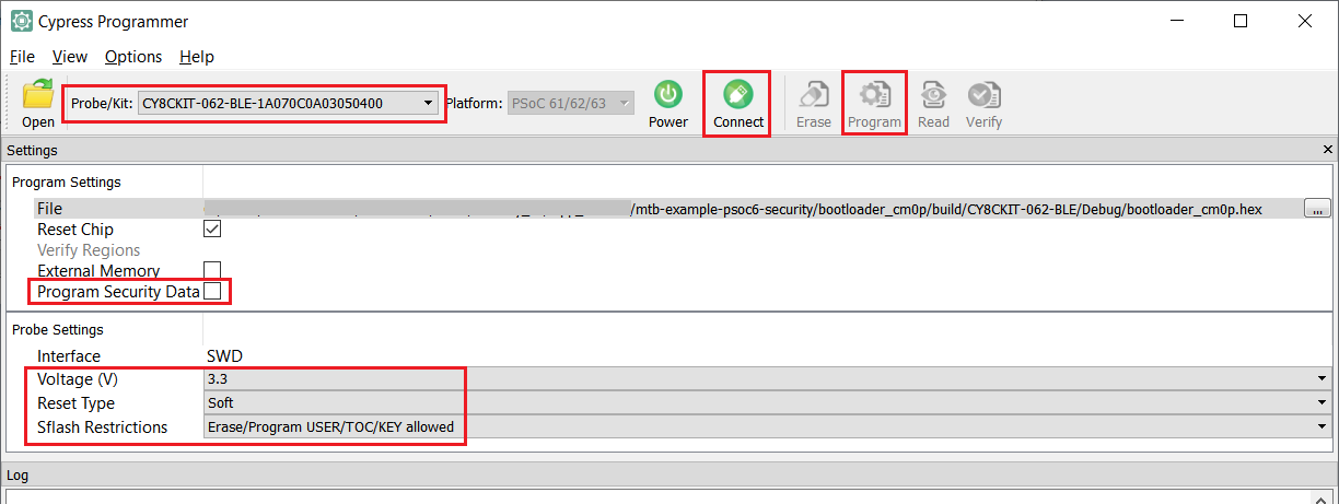
Dual CPU design considerations
Making use of the dual-CPU feature in the PSoC™ 62/63 adds yet another security option. Although the two CPUs share the same internal Flash and SRAM, the SMPUs allow you to isolate sections of memory as if each CPU had its own memory. The IPC block provides a convenient way to pass 32-bit words between the two CPUs. If large amounts of data need to be transferred between the two CPUs, a section of the SRAM can be configured to be accessible by both CPUs. This way you can pass a pointer to a structure that includes a large buffer of data.
One way to make use of the dual-CPU feature for added security is to divide your application between SECURE and NON-SECURE code. Run the SECURE code in CM0+ and the NON-SECURE part of the application on CM4. This way you can limit the SECURE code and more thoroughly test it. Also, you would run the more complicated software such was Wi-Fi or Bluetooth® stacks that are more difficult to test on CM4.
One example is a Wi-Fi enabled door lock with finger print sensor. The code that operates the SECURE part of the door lock such as the finger print sensor and the hardware mechanism would run on CM0+ and the Wi-Fi stack would run on CM4.
Summary
This application note has shown how the PSoC™ 6 MCU hardware can be used to create a secured system. Every application has different requirements and the flexibility of the PSoC™ security hardware can be used to adapt to those needs. As mentioned earlier, it is important to think about security from the beginning of your project and analyze each point of access to the code and data, do not let security be an afterthought. Determining up front what is required will reduce the chance that you will need to re-architect your project late in your project schedule.
Appendix A - Code example of a security application template in this document describes a code example that can be used as a template to implement what has been discussed in the application note.
Appendix A - Code example of a security application
template
This appendix explains a code example that demonstrates most of the topics discussed in this application note. The code example CE234992 PSoC™ 6 MCU: Security Template, includes all the source code, Makefiles, and scripts required to build, link, and sign the code. The following is a list of features demonstrated:
-
Bootloader based on the industry standard MCUboot (CM0+)
-
Bootloader is cryptographically signed
-
Dual-CPU operation; user applications for both CM0+ and CM4
-
Supports device firmware update (DFU) with the standard UART interface
-
FreeRTOS running on CM4
-
CM0+ and CM4 application bundle signed
-
Full Chain of Trust
-
Isolated CPUs using SMPUs
-
Communication between CM0+ and CM4
This code example consists of the following three projects:
-
proj_btldr_cm0p (MCUboot bootloader CM0+)
-
proj_cm0p (CM0+ user project)
-
proj_cm4 (CM4 user project)
Figure 14. Application file structure

Bootup flow
This flow assumes that the device has already been moved to the SECURE lifecycle stage.
-
CM0+ starts from reset.
-
CM0+ executes the internal ROM code that does the following:
- Loads the trim values
- Verifies that the second half of the boot code (Flash boot) and the user’s public key are intact
-
The Flash boot code verifies that the user’s bootloader (proj_btldr_cm0p) is signed by the owner of the public key (RSA-2048) and that the code has not been corrupted.
-
Jumps to the bootloader.Figure 15. Application boot flow
-
The bootloader configures the protection units to isolate CM0+ and CM4 projects.
-
Review the code in the /proj_btldr_cm0p/cy_ps_prot_units.c file to learn how the SMPUs and Protection Context registers are set up.
-
The code checks to see if there is a newer version of the user application bundle, which includes both the CM0+ and CM4 applications. If a newer version is available, the code does the following:
- Copies the new firmware image to the primary slot
- Validates the new firmware image with the ECC key
- If the image is verified, jumps to the user CM0+ project (proj_cm0p)
-
The CM0+ application enables CM4 and continues to execute its application.
-
In the associated code examples that is used to demonstrate the firmware flow, the CM0+ application is nothing more than a LED blink application. You can remove these two lines of code and replace it with your own application.
-
CM4 comes out of reset, and does the following:
- Configures the required hardware
- Initializes a few FreeRTOS tasks
One of these tasks is the DFU (device firmware upgrade), which listens on a serial port waiting for a command to start the download of a new version of the application bundle.
Application Chain of Trust (CoT)
The following diagram illustrates the Chain of Trust for this project. Note that there are two different types of crypto keys used to validate the full application. The PSoC™ 62/63 MCU natively uses an RSA-2048 key; the bootloader based on MCUboot uses ECC by default.
Figure 16. Chain of Trust

Project memory map
The memory map for the example project is shown below. The diagrams also show the access of the memory by the protection context.
The flash memory is broken up into four major areas:
-
Bootloader
-
Protected memory
-
Primary slot
-
Secondary slot
The bootloader area is not intended to be updated in the field and therefore must be thoroughly tested before release. Most of the code in the bootloader area is a port from MCUboot, the industry standard bootloader infrastructure.
The protected memory region contains the sensitive data; only CM0+ has direct access to it. While some of this data could be preprogrammed from the factory, other parts could be used for dynamic storage.
The primary slot is the area in which the application code is executed. Both CM0+ and CM4 execute code in this region. Only CM0+ can write to this area while executing the bootloader; CM4 cannot write to this region.
The secondary slot is the area used to store an updated project. In most applications, it is up to CM4 to perform the operation because it is most likely to be the CPU communicating to the outside world via Wi-Fi, Bluetooth®, or DFU. If required, the CM0+ application code can update the code in the secondary slot.
| Protection context (PC) | CPU access | Notes |
|---|---|---|
0 | CM0+ | Default state of CM0+. It is used to configure the protection units at the beginning of the bootloader code. All memory and registers are accessible in PC=0; all system calls operate at PC=0 as well. |
1 | CM0+ | The bootloader runs at Protection Context 1 after protection units have been configured. All areas that need to be accessed by the bootloader have PC=1 as part of their mask. |
2 | CM0+ | Reserved for the protected memory that could be used for secure storage. CM0+ must switch to PC=2 while accessing the area. |
4 | CM4 | Domain of the CM4 CPU. It must access its portion of the primary slot and all of the secondary flash area. The CM4 code is responsible for updating the code in the secondary slot. |
Figure 17. Project flash memory maps for 512K, 1M, and 2M flash parts

Figure 18. Project SRAM memory maps for 512K, 1M, and 2M flash parts

Appendix B - Creating crypto key pairs
The ModusToolbox™ software installation includes the tools required to generate and format the private/public key pairs, including OpenSSL. However, the Python 3.8.10 or later should be installed separately and added to the top of the system path in environmental variables. To access these tools without updating any system paths, use the “Modus Shell” command-line shell.
The PSoC™ 62/63 Flash boot code requires an RSA-2048 public key to be stored in SFlash, and the first user code to be signed with the corresponding private key to boot in the SECURE lifecycle stage. In the companion code example (CE234992), “proj_btldr_cm0p” is the first user code.
The proj_btldr_cm0p project is a port of the open source MCUboot project. This project boots the actual user project code; it also requires a crypto key pair to sign and validate the user project. MCUboot uses the ECDSA algorithm instead of RSA, so it cannot use the same RSA key that is used by Flash boot. This appendix provides details of what is required to generate the keys for both RSA and ECC.
Generating the RSA key pair
The companion code example (CE234992) includes a default key that is already generated. This key is sufficient for development, but do not use this for production. These steps will generate a custom private/public key pair in the keys directory and generate a C-compatible public key, but you must manually copy the generated C code to the cy_ps_keystorage.c file.
Do the following to generate a new custom key pair:
-
Start the “modus-shell” application that is installed along with ModusToolbox™ software.
-
Navigate to mtb-psoc6-example-security/proj_btldr_cm0p directory.
-
Execute the command make rsa_keygen.
-
This command creates a file in the keys subdirectory called rsa_to_c_generated.txt.
-
Copy the following arrays from the rsa_to_c_generated.txt file and replace those in cy_ps_keystorage.c. .moduleData[] .expData[] .barrettData[] .inverseModuleData[] .rBarData[]
Generating the ECC key pair
Generating the ECC key pair required for the bootloader (MCUboot) is similar to the RSA key pair generation but simpler.
-
Start the modus-shell application.
-
Navigate to the mtb-psoc6-example-security/bootloader_cmp0 directory.
-
Execute the command make ecc_keygen.
This will create the following files in the keys folder:
-
cypress-test-ec-p256.pem (private key)
-
cypress-test-ec-p256.pub (public key in a C-like array)
-
ecc-public-key-p256.h (public-key header file in C-like array)
The public key will automatically be incorporated into the MCUboot build, you do not need to edit the files.
Example RSA private/public key files
The “make rsa_keygen” command creates the following two other files in the keys directory:
-
rsa_private_generated.txt
-
rsa_public_generated.txt
These files are generated by OpenSSL and are used to create the rsa_to_c_generated.txt file.
The rsa_private_generated.txt private key file will look like as follows:
-----BEGIN RSA PRIVATE KEY-----
MIIEowIBAAKCAQEAt8ygBxZNdfUHz7m7sQXPYinpAuiO5aFoEJsiopNTScohuCGA
BTtReTI7V5x8h/etDrnWG+AhYNHKT+uh7O5ZFZU7MBd/69n9jBWFJDfbJhXfvv69
r7uPwVJK705GLkUnVNCxHiz6/CGCYs6RyWQ9xQxMuSqCCjKOxhk5x0SwjMeAh3Pm
MR+AZFd2W7fkADjFDODgb9mDGp+49zO+v/nGTgNR5PEbMbBwjAjcNyxeM5LrtzTz
8pongkeg/XBBsaDaZPpqHm67HknMAHUeTKACx9vLHHksjm8w6n55/QGwiGBUd1fk
zOgQii4rGluKoCfT76sqdpdCQuahF2EACTb0MwIDAQABAoIBAF6UUZTUCTA10rs1
3DuPvdPJtTnl6gKIOECzU/NM1IMYHJnfwzzt9VLkYl0HDZ35+XemcWMOxp5H1k+h
9UUysWzFyhtJPG5lUm+Pc1/bzk2e2/AwrfOMFMFqU10pbjvJIiAm872Pb+fmZm3p
1mNHzfFkDucJ1Ljio02VFYJQ+ni2IIJGi/QxRBOS0I5PAIUQCuLoiRx3mO61uJC5
DaZGZLmO/tpz1FNGNMHuP+iQH5UlwIRhqSnEH0dOUWikUhZU2d3MwEJqS0I/txl2
nsUqsxooG7FNrtvo2QzSXR0mYXJmloEuFJpwSrMsQnlq0uKl3SBXkfhoCojOwNrj
sZetAOECgYEA7ELrvtqC6fTQFiN49L3W+/WdMLMtPpguUhWGZB6A+/HaTM30OxMj
Ks9JXdeA+LMw9k3Q9ukAbisy/PphCShiHphbhzPzFQvluXXswh/kh82X+TFEs+jt
9ceAuA45cULZHPXSqljmHet4wXeiDH1tCufG6VP3JL9OhGkRqWZwJ30CgYEAxyep
qKNsdVzdAHFVcX2Wd7kUSbS2TrmIos1CmyjdfEtPbWjzWbRCFzAjpqVDjNA67ZeH
DBo68xjaNvOunKBj/Sc1FQXprPXbPc0T6W4n6J2w0C1jabnCiXamHKoaNenbze5+
K5nlLyuLnnyjWt8p63JvH1cUU61djq+M+VTnOW8CgYEAk7NmhANBMpfc+uokNQT1
gMDVC1wInggvdRuFz9OOGXPiYH+k/sWBB8Nc/3C5bUFBC8osKCAUJ8uT7bltrnbz
mGLxXX3pqq+sZxxE7jtX+FpcduoJJFwrX6rgWrBx0s/SwZsgn2RCQFQ0QubShPJo
mBe8L6RRbkS3BmpVI00qMlUCgYBfsstv4bfIXatE/zDTrEmVljYNhOzlv3nM4V1U
ObrUc0vjgz8Mp/XqNpOrDFb9X0Ix0VJvmlshXZveNBJ/6QKjLyfuxjyXhDyp4dXj
oa9DtCK2pljTARReAcmolISry4h32FaAlR7wH7ijm7jTfdEi9oY3RRzbaL9ARVM0
rHu/uQKBgB7cZeXHu2zPhKN91uuB5NI8N3SoGhWajjODM8Nb4MQdWFl6BHvGbl0Z
Ld12+nuRnzim7rpS8vNlVRS2KnmTvdpGEb8yW5hMxGN3J8yKg8GslbMaJ4rmlh7j
GBZrx4ttq9fjipfgTYqN1QTWabxRqG8S0LTIjWpiVZMZOGOfSOLt
-----END RSA PRIVATE KEY-----
The “rsa_public_generated.txt” public key file will look like as follows:
-----BEGIN PUBLIC KEY-----
MIIBIjANBgkqhkiG9w0BAQEFAAOCAQ8AMIIBCgKCAQEAt8ygBxZNdfUHz7m7sQXP
YinpAuiO5aFoEJsiopNTScohuCGABTtReTI7V5x8h/etDrnWG+AhYNHKT+uh7O5Z
FZU7MBd/69n9jBWFJDfbJhXfvv69r7uPwVJK705GLkUnVNCxHiz6/CGCYs6RyWQ9
xQxMuSqCCjKOxhk5x0SwjMeAh3PmMR+AZFd2W7fkADjFDODgb9mDGp+49zO+v/nG
TgNR5PEbMbBwjAjcNyxeM5LrtzTz8pongkeg/XBBsaDaZPpqHm67HknMAHUeTKAC
x9vLHHksjm8w6n55/QGwiGBUd1fkzOgQii4rGluKoCfT76sqdpdCQuahF2EACTb0
MwIDAQAB
-----END PUBLIC KEY-----
Editing the RSA key C file (cy_ps_keystorage.c)
The following is an example of the cy_ps_keystorage.c file. The sections shown in italics are areas that need to be replaced with the contents of the rsa_to_c_generated.txt file after running the make rsa_keygen command.
The final step to updating the public key in the secure image is to copy the code in the generated rsa_to_c_generated.txt file to the cy_keystorage.c source file, which is part of the secure image project.
An example of this file after being updated is shown below. The replacement code from the generated key data is shown below in italics.
/***************************************************************************//**
* \file cy_ps_keystorage.c
* \version 1.20
*
* \brief
* Secure key storage for application usage.
*
********************************************************************************
* \copyright
* Copyright 2017-2018, Cypress Semiconductor Corporation. All rights reserved.
* You may use this file only in accordance with the license, terms, conditions,
* disclaimers, and limitations in the end user license agreement accompanying
* the software package with which this file was provided.
*******************************************************************************/

#include <source/cy_ps_keystorage.h>

#if defined(__cplusplus)
extern "C" (
#endif

/* Secure Key Storage (Note: Ensure that the alignment matches the Protection unit configuration) */
CY_ALIGN(1024) __USED const uint8_t CySecureKeyStorage[CY_PS_SECURE_KEY_ARRAY_SIZE][CY_PS_SECURE_KEY_LENGTH] = (
    (0x00u), /* Insert user key #1 values */
    (0x00u), /* Insert user key #2 values */
    (0x00u), /* Insert user key #3 values */
    (0x00u)  /* Insert user key #4 values */
);

/* Public key in SFlash */
CY_SECTION(".cy_sflash_public_key") __USED const cy_ps_stc_public_key_t cy_publicKey =
(
    .objSize = sizeof(cy_ps_stc_public_key_t),
    .signatureScheme = CY_PS_PUBLIC_KEY_RSA_2048,
    .publicKeyStruct =
    (
        .moduloAddr         = (uint32_t)&(SFLASH->PUBLIC_KEY) + offsetof(cy_ps_stc_public_key_t, moduloData),
        .moduloSize         = CY_PS_PUBLIC_KEY_SIZEOF_BYTE * CY_PS_PUBLIC_KEY_MODULOLENGTH,
        .expAddr            = (uint32_t)&(SFLASH->PUBLIC_KEY) + offsetof(cy_ps_stc_public_key_t, expData),
        .expSize            = CY_PS_PUBLIC_KEY_SIZEOF_BYTE * CY_PS_PUBLIC_KEY_EXPLENGTH,
        .barrettAddr        = (uint32_t)&(SFLASH->PUBLIC_KEY) + offsetof(cy_ps_stc_public_key_t, barrettData),
        .inverseModuloAddr  = (uint32_t)&(SFLASH->PUBLIC_KEY) + offsetof(cy_ps_stc_public_key_t, inverseModuloData),
        .rBarAddr           = (uint32_t)&(SFLASH->PUBLIC_KEY) + offsetof(cy_ps_stc_public_key_t, rBarData),
    ),
    .moduloData =
    (
        0x33u, 0xF4u, 0x36u, 0x09u, 0x00u, 0x61u, 0x17u, 0xA1u,
        0xE6u, 0x42u, 0x42u, 0x97u, 0x76u, 0x2Au, 0xABu, 0xEFu,
        0xD3u, 0x27u, 0xA0u, 0x8Au, 0x5Bu, 0x1Au, 0x2Bu, 0x2Eu,
        0x8Au, 0x10u, 0xE8u, 0xCCu, 0xE4u, 0x57u, 0x77u, 0x54u,
        0x60u, 0x88u, 0xB0u, 0x01u, 0xFDu, 0x79u, 0x7Eu, 0xEAu,
        0x30u, 0x6Fu, 0x8Eu, 0x2Cu, 0x79u, 0x1Cu, 0xCBu, 0xDBu,
        0xC7u, 0x02u, 0xA0u, 0x4Cu, 0x1Eu, 0x75u, 0x00u, 0xCCu,
        0x49u, 0x1Eu, 0xBBu, 0x6Eu, 0x1Eu, 0x6Au, 0xFAu, 0x64u,
        0xDAu, 0xA0u, 0xB1u, 0x41u, 0x70u, 0xFDu, 0xA0u, 0x47u,
        0x82u, 0x27u, 0x9Au, 0xF2u, 0xF3u, 0x34u, 0xB7u, 0xEBu,
        0x92u, 0x33u, 0x5Eu, 0x2Cu, 0x37u, 0xDCu, 0x08u, 0x8Cu,
        0x70u, 0xB0u, 0x31u, 0x1Bu, 0xF1u, 0xE4u, 0x51u, 0x03u,
        0x4Eu, 0xC6u, 0xF9u, 0xBFu, 0xBEu, 0x33u, 0xF7u, 0xB8u,
        0x9Fu, 0x1Au, 0x83u, 0xD9u, 0x6Fu, 0xE0u, 0xE0u, 0x0Cu,
        0xC5u, 0x38u, 0x00u, 0xE4u, 0xB7u, 0x5Bu, 0x76u, 0x57u,
        0x64u, 0x80u, 0x1Fu, 0x31u, 0xE6u, 0x73u, 0x87u, 0x80u,
        0xC7u, 0x8Cu, 0xB0u, 0x44u, 0xC7u, 0x39u, 0x19u, 0xC6u,
        0x8Eu, 0x32u, 0x0Au, 0x82u, 0x2Au, 0xB9u, 0x4Cu, 0x0Cu,
        0xC5u, 0x3Du, 0x64u, 0xC9u, 0x91u, 0xCEu, 0x62u, 0x82u,
        0x21u, 0xFCu, 0xFAu, 0x2Cu, 0x1Eu, 0xB1u, 0xD0u, 0x54u,
        0x27u, 0x45u, 0x2Eu, 0x46u, 0x4Eu, 0xEFu, 0x4Au, 0x52u,
        0xC1u, 0x8Fu, 0xBBu, 0xAFu, 0xBDu, 0xFEu, 0xBEu, 0xDFu,
        0x15u, 0x26u, 0xDBu, 0x37u, 0x24u, 0x85u, 0x15u, 0x8Cu,
        0xFDu, 0xD9u, 0xEBu, 0x7Fu, 0x17u, 0x30u, 0x3Bu, 0x95u,
        0x15u, 0x59u, 0xEEu, 0xECu, 0xA1u, 0xEBu, 0x4Fu, 0xCAu,
        0xD1u, 0x60u, 0x21u, 0xE0u, 0x1Bu, 0xD6u, 0xB9u, 0x0Eu,
        0xADu, 0xF7u, 0x87u, 0x7Cu, 0x9Cu, 0x57u, 0x3Bu, 0x32u,
        0x79u, 0x51u, 0x3Bu, 0x05u, 0x80u, 0x21u, 0xB8u, 0x21u,
        0xCAu, 0x49u, 0x53u, 0x93u, 0xA2u, 0x22u, 0x9Bu, 0x10u,
        0x68u, 0xA1u, 0xE5u, 0x8Eu, 0xE8u, 0x02u, 0xE9u, 0x29u,
        0x62u, 0xCFu, 0x05u, 0xB1u, 0xBBu, 0xB9u, 0xCFu, 0x07u,
        0xF5u, 0x75u, 0x4Du, 0x16u, 0x07u, 0xA0u, 0xCCu, 0xB7u,
    ),
    .expData =
    (
        0x01u, 0x00u, 0x01u, 0x00u,
    ),
    .barrettData =
    (
        0xDCu, 0x40u, 0x33u, 0x8Au, 0x4Eu, 0xA6u, 0xF1u, 0x08u,
        0x2Au, 0x7Bu, 0x5Cu, 0x77u, 0xC9u, 0xB1u, 0x95u, 0x68u,
        0x94u, 0xF2u, 0x80u, 0x0Eu, 0xA7u, 0x99u, 0xE5u, 0xBDu,
        0x07u, 0x91u, 0x0Cu, 0x66u, 0x62u, 0x3Du, 0x1Eu, 0x02u,
        0x6Cu, 0x12u, 0x3Bu, 0x79u, 0xE0u, 0xB6u, 0x81u, 0xB4u,
        0xACu, 0x85u, 0x75u, 0x44u, 0x95u, 0x0Du, 0xC7u, 0xE9u,
        0x69u, 0x7Du, 0xD3u, 0x30u, 0x4Bu, 0x57u, 0x4Du, 0x2Fu,
        0x6Eu, 0x80u, 0x51u, 0xC0u, 0x72u, 0x4Bu, 0x23u, 0x76u,
        0x82u, 0x91u, 0x98u, 0x47u, 0xFEu, 0x4Fu, 0xBCu, 0xBFu,
        0xA5u, 0x84u, 0x26u, 0xF0u, 0x90u, 0x62u, 0xC1u, 0x0Fu,
        0xFAu, 0x81u, 0xBAu, 0x57u, 0xDFu, 0x98u, 0x00u, 0xE3u,
        0xC6u, 0xACu, 0x99u, 0x82u, 0xFAu, 0x29u, 0x61u, 0xF3u,
        0x37u, 0x7Au, 0x61u, 0x09u, 0x25u, 0x92u, 0xCFu, 0xDFu,
        0x17u, 0x20u, 0x46u, 0x8Du, 0xBFu, 0x88u, 0xE7u, 0x0Bu,
        0xB5u, 0xAFu, 0xCEu, 0x03u, 0x8Au, 0xEAu, 0x33u, 0xC4u,
        0x8Cu, 0x1Bu, 0x44u, 0x41u, 0xC6u, 0x9Au, 0xCDu, 0x57u,
        0x5Fu, 0x59u, 0x6Eu, 0x1Eu, 0x1Cu, 0xDBu, 0xD7u, 0x37u,
        0x38u, 0x98u, 0xF6u, 0x0Bu, 0x3Du, 0xCDu, 0x11u, 0xA5u,
        0xF0u, 0x1Fu, 0x13u, 0x3Eu, 0x46u, 0x0Bu, 0xADu, 0x07u,
        0xA3u, 0x6Fu, 0x8Fu, 0xD5u, 0xCEu, 0xD8u, 0xA6u, 0x36u,
        0x8Eu, 0x39u, 0xDCu, 0xDCu, 0x07u, 0x6Fu, 0xE8u, 0x3Au,
        0x64u, 0x71u, 0x10u, 0xE1u, 0xCDu, 0x20u, 0xDFu, 0x4Bu,
        0xC8u, 0xA3u, 0x1Bu, 0x89u, 0x20u, 0x35u, 0x51u, 0x8Fu,
        0xA6u, 0x48u, 0x1Au, 0xF5u, 0xD5u, 0xF2u, 0x65u, 0x8Fu,
        0x3Au, 0x55u, 0x3Fu, 0x7Eu, 0x4Bu, 0x44u, 0x7Fu, 0xBAu,
        0x27u, 0xF4u, 0x19u, 0x2Cu, 0x53u, 0x06u, 0x75u, 0xB8u,
        0xB8u, 0xC4u, 0x8Fu, 0xCBu, 0xC9u, 0xE5u, 0xFBu, 0x91u,
        0xAAu, 0x4Du, 0x3Bu, 0xD2u, 0xA3u, 0x2Au, 0x36u, 0x2Fu,
        0xC9u, 0xBFu, 0xCCu, 0x8Du, 0xF9u, 0x3Eu, 0x5Fu, 0x9Eu,
        0xEEu, 0x19u, 0xF0u, 0xD5u, 0x58u, 0xE0u, 0x07u, 0x1Bu,
        0xBDu, 0xF1u, 0x42u, 0xF9u, 0xB2u, 0xC9u, 0x07u, 0x3Cu,
        0x44u, 0x67u, 0xD5u, 0x32u, 0x00u, 0x14u, 0x90u, 0x64u,
        0x01u, 0x00u, 0x00u, 0x00u,
    ),
    .inverseModuloData =
    (
        0x05u, 0xD9u, 0x5Au, 0x11u, 0xBDu, 0x82u, 0x6Au, 0x74u,
        0x24u, 0x61u, 0xBBu, 0x30u, 0x03u, 0x6Du, 0x5Bu, 0xEDu,
        0x61u, 0xCEu, 0x5Cu, 0x32u, 0xBBu, 0x1Du, 0x3Fu, 0x38u,
        0xB8u, 0x75u, 0x36u, 0x1Au, 0x6Cu, 0x2Du, 0x46u, 0x3Cu,
        0x1Au, 0x61u, 0xE1u, 0x63u, 0x2Cu, 0x8Fu, 0x49u, 0x80u,
        0xCAu, 0xFFu, 0x51u, 0x5Fu, 0xC6u, 0x2Au, 0x2Au, 0x38u,
        0xCFu, 0x6Du, 0x35u, 0x87u, 0xBCu, 0x74u, 0x47u, 0x2Fu,
        0xE5u, 0x7Fu, 0xC3u, 0x18u, 0x8Du, 0x9Au, 0x60u, 0xCAu,
        0xEFu, 0x84u, 0x2Eu, 0xF2u, 0x6Eu, 0x8Du, 0x88u, 0xC3u,
        0x13u, 0x9Du, 0x4Eu, 0x81u, 0x34u, 0xFDu, 0x21u, 0x18u,
        0xDDu, 0xE7u, 0xD3u, 0x71u, 0x51u, 0x49u, 0x6Eu, 0xF9u,
        0x24u, 0xAFu, 0x4Eu, 0x94u, 0x23u, 0xD8u, 0x05u, 0x64u,
        0x42u, 0x74u, 0x48u, 0x02u, 0x54u, 0x8Bu, 0xE4u, 0x7Bu,
        0xA9u, 0x69u, 0x3Du, 0x56u, 0xF0u, 0xD1u, 0xA0u, 0x39u,
        0x86u, 0x11u, 0x1Eu, 0xEFu, 0x0Bu, 0x64u, 0x60u, 0x7Du,
        0x32u, 0x8Fu, 0x4Bu, 0x01u, 0xC6u, 0x8Eu, 0x84u, 0x8Du,
        0xAFu, 0xD6u, 0x1Du, 0x0Fu, 0x1Cu, 0x38u, 0x15u, 0x4Bu,
        0xF3u, 0x8Cu, 0xB1u, 0xF0u, 0x05u, 0x96u, 0xFAu, 0x97u,
        0x22u, 0x4Eu, 0x2Du, 0x6Bu, 0xDBu, 0x7Du, 0x31u, 0x92u,
        0x8Eu, 0x3Bu, 0x33u, 0x5Bu, 0xA2u, 0xFDu, 0xF8u, 0x12u,
        0x55u, 0x15u, 0xD3u, 0x39u, 0xE3u, 0x83u, 0x48u, 0xA8u,
        0x02u, 0x46u, 0x40u, 0x17u, 0x92u, 0x4Du, 0x89u, 0x6Du,
        0x86u, 0xCCu, 0x40u, 0x07u, 0x16u, 0x82u, 0x68u, 0xE7u,
        0x28u, 0xB6u, 0xF9u, 0x52u, 0xFCu, 0x8Fu, 0x84u, 0x84u,
        0x4Bu, 0xBBu, 0x7Bu, 0x20u, 0xEEu, 0x3Du, 0x14u, 0x26u,
        0x5Eu, 0x17u, 0xC7u, 0xFFu, 0x4Eu, 0xBAu, 0xAEu, 0x81u,
        0x36u, 0x1Du, 0x10u, 0xE1u, 0x37u, 0x25u, 0xBEu, 0x02u,
        0x84u, 0x09u, 0x54u, 0xC8u, 0xD5u, 0x09u, 0x78u, 0xD4u,
        0x34u, 0x4Au, 0x03u, 0x5Bu, 0xA3u, 0x6Du, 0xEEu, 0x36u,
        0xACu, 0xF2u, 0xE9u, 0x3Eu, 0x67u, 0xF4u, 0xD0u, 0xA5u,
        0x1Cu, 0x32u, 0xDEu, 0x56u, 0x84u, 0x5Cu, 0xB6u, 0xA7u,
        0xE3u, 0x3Du, 0xF6u, 0xC2u, 0x44u, 0xFDu, 0xFAu, 0xC0u,
    ),
    .rBarData =
    (
        0xCDu, 0x0Bu, 0xC9u, 0xF6u, 0xFFu, 0x9Eu, 0xE8u, 0x5Eu,
        0x19u, 0xBDu, 0xBDu, 0x68u, 0x89u, 0xD5u, 0x54u, 0x10u,
        0x2Cu, 0xD8u, 0x5Fu, 0x75u, 0xA4u, 0xE5u, 0xD4u, 0xD1u,
        0x75u, 0xEFu, 0x17u, 0x33u, 0x1Bu, 0xA8u, 0x88u, 0xABu,
        0x9Fu, 0x77u, 0x4Fu, 0xFEu, 0x02u, 0x86u, 0x81u, 0x15u,
        0xCFu, 0x90u, 0x71u, 0xD3u, 0x86u, 0xE3u, 0x34u, 0x24u,
        0x38u, 0xFDu, 0x5Fu, 0xB3u, 0xE1u, 0x8Au, 0xFFu, 0x33u,
        0xB6u, 0xE1u, 0x44u, 0x91u, 0xE1u, 0x95u, 0x05u, 0x9Bu,
        0x25u, 0x5Fu, 0x4Eu, 0xBEu, 0x8Fu, 0x02u, 0x5Fu, 0xB8u,
        0x7Du, 0xD8u, 0x65u, 0x0Du, 0x0Cu, 0xCBu, 0x48u, 0x14u,
        0x6Du, 0xCCu, 0xA1u, 0xD3u, 0xC8u, 0x23u, 0xF7u, 0x73u,
        0x8Fu, 0x4Fu, 0xCEu, 0xE4u, 0x0Eu, 0x1Bu, 0xAEu, 0xFCu,
        0xB1u, 0x39u, 0x06u, 0x40u, 0x41u, 0xCCu, 0x08u, 0x47u,
        0x60u, 0xE5u, 0x7Cu, 0x26u, 0x90u, 0x1Fu, 0x1Fu, 0xF3u,
        0x3Au, 0xC7u, 0xFFu, 0x1Bu, 0x48u, 0xA4u, 0x89u, 0xA8u,
        0x9Bu, 0x7Fu, 0xE0u, 0xCEu, 0x19u, 0x8Cu, 0x78u, 0x7Fu,
        0x38u, 0x73u, 0x4Fu, 0xBBu, 0x38u, 0xC6u, 0xE6u, 0x39u,
        0x71u, 0xCDu, 0xF5u, 0x7Du, 0xD5u, 0x46u, 0xB3u, 0xF3u,
        0x3Au, 0xC2u, 0x9Bu, 0x36u, 0x6Eu, 0x31u, 0x9Du, 0x7Du,
        0xDEu, 0x03u, 0x05u, 0xD3u, 0xE1u, 0x4Eu, 0x2Fu, 0xABu,
        0xD8u, 0xBAu, 0xD1u, 0xB9u, 0xB1u, 0x10u, 0xB5u, 0xADu,
        0x3Eu, 0x70u, 0x44u, 0x50u, 0x42u, 0x01u, 0x41u, 0x20u,
        0xEAu, 0xD9u, 0x24u, 0xC8u, 0xDBu, 0x7Au, 0xEAu, 0x73u,
        0x02u, 0x26u, 0x14u, 0x80u, 0xE8u, 0xCFu, 0xC4u, 0x6Au,
        0xEAu, 0xA6u, 0x11u, 0x13u, 0x5Eu, 0x14u, 0xB0u, 0x35u,
        0x2Eu, 0x9Fu, 0xDEu, 0x1Fu, 0xE4u, 0x29u, 0x46u, 0xF1u,
        0x52u, 0x08u, 0x78u, 0x83u, 0x63u, 0xA8u, 0xC4u, 0xCDu,
        0x86u, 0xAEu, 0xC4u, 0xFAu, 0x7Fu, 0xDEu, 0x47u, 0xDEu,
        0x35u, 0xB6u, 0xACu, 0x6Cu, 0x5Du, 0xDDu, 0x64u, 0xEFu,
        0x97u, 0x5Eu, 0x1Au, 0x71u, 0x17u, 0xFDu, 0x16u, 0xD6u,
        0x9Du, 0x30u, 0xFAu, 0x4Eu, 0x44u, 0x46u, 0x30u, 0xF8u,
        0x0Au, 0x8Au, 0xB2u, 0xE9u, 0xF8u, 0x5Fu, 0x33u, 0x48u,
    ),
);

#if defined(__cplusplus)
)
#endif
Appendix C - Debug port access settings
Table 13 shows the memory location for each of the three type of debug access restrictions (SECURE, DEAD, and NORMAL). SARs and DARs are stored in eFuse, but NARs are stored in SFlash. For eFuse, this is only the read location; the eFuse write location is in a different memory location and set up as one byte per bit.
| Access restriction | ACCESS_RESTRICT0 (ADDR) | ACCESS_RESTRICT1 (ADDR) | Storage area |
|---|---|---|---|
SECURE | 0x402C_0829* | 0x402C_082A* | eFuse |
DEAD | 0x402C_0827* | 0x402C_0828* | eFuse |
NORMAL | 0x1600_1A00 | 0x1600_1A01 | SFlash |
Debug access settings
The format for all three types of access restrictions (SECURE, DEAD, NORMAL) is the same, although stored in different locations. The default state of all debug access restrictions is zero, which means that all debug ports are open for full access.
This section defines the location and definition of each of those parameters. Figure 19 and Figure 20 represent the format for the 2-byte access restriction structure.
Figure 19. ACCESS_RESTRICT0

Figure 20. ACCESS_RESTRICT1
Table 14 Access restriction parameters.
| Field | Value | Description |
|---|---|---|
MMIO_Allowed | 0x0: All MMIO register 0x1: Only IPC ports 0, 1, and 2 0x2 or 0x3: No MMIO access | Defines what MMIO register are accessible via the SYS_AP. IPC ports 0, 1, and 3 are used for system calls required for programming of the device. |
SFlash_Allowed | 0: Entire SFlash accessible 1: Bottom ½ of SFlash accessible 2: Bottom ¼ of SFlash accessible 3: No access allowed to SFlash | This field indicates what portion of the SFlash main region is accessible through the SYS_AP. Only a portion of flash starting at the bottom of the area is exposed. Valid only if SYS_DISABLE=0 and SYS_AP_MPU_ENABLE=1. |
SYS_AP_MPU_ENABLE | 0x0: SYS_AP MPU disabled 0x1: SYS_AP MPU enabled | SYS_AP_DISABLE must not be disabled for the MPU to be enabled. |
SYS_AP_DISABLE | 0x0: SYS_AP not disabled 0x1: SYS_AP disabled | Disables the SYS_AP |
CM4_DISABLE | 0x0: CM4_AP not disabled 0x1: CM4_AP disabled | Disables the CM4_AP |
CM0_DISABLE | 0x0: CM0_AP not disabled 0x1: CM0_AP disabled | Disables the CM0_AP |
DIRECT_EXE_DISABLE | 0x0: Not disabled 0x1: Disable | Disable Direct Execture system call functionality. |
SMIF_XIP_ALLOWED | 0x0: Entire Region 0x1: Nothing | This field indicates what portion of XIP is accessible through the system access port. |
SRAM_ALLOWED | 0x0: entire region 0x1: 7/8 0x2: 3/4th 0x3: 1/2 0x4: 1/4th 0x5: 1/8th 0x6: 1/16th 0x7: nothing | This field indicates what portion of the SRAM region is accessible through the SYS_AP. Only a portion of SRAM starting at the bottom of the area is exposed. Valid only if SYS_DISABLE=0 and SYS_AP_MPU_ENABLE=1. |
FLASH_ALLOWED | 0x0: entire region 0x1: 7/8 0x2: 3/4th 0x3: 1/2 0x4: 1/4th 0x5: 1/8th 0x6: 1/16th 0x7: nothing | This field indicates what portion of the flash main region is accessible through the SYS_AP. Only a portion of flash starting at the bottom of the area is exposed. Valid only if SYS_DISABLE=0 and SYS_AP_MPU_ENABLE=1. |
Firmware control of Debug Port
If any of the three debug access ports (CM0+, CM4, SYS) are disabled in the SECURE life cycle stage, there is no way to connect to those ports. If any of the debug ports are not disabled in the SECURE life cycle stage, it is possible for the debug port to be opened either automatically or with firmware. You can disable any combination of the three access ports, and the ports not disabled may be connected to an external programmer/debugger. The 2nd generation parts are slightly different than the 1st generation parts as described in the following sections.
1st generation PSoC 6 devices
In the SECURE life cycle stage, if the debug access ports were not disabled, a debugger/programmer cannot connect to the enabled access port until the GPIOs used for debugging are configured properly. This can be accomplished within the user’s firmware with the code shown in section 9.2.3.
2nd generation PSoC 6 devices
The 2nd generation parts have an additional option for configuring the debug ports. A flag in TOC2 Flash boot options, allow the user to set the default state of the debug ports when in the SECURE life cycle stage. If the “SWJ pin state” bits are set to 0x10, the GPIOs will be automatically configured to allow connection by a debugger/programmer hardware without additional user firmware. See the table below for the TOC2 Flash boot flags for the SWJ pin state.
SWJ (debug) pin state | [6:5] | 0x00 = Do not enable SWJ pins 0x01 = Do not enable SWJ pins 0x10 = Enable SWJ pins 0x11 = Do not enable SWJ pins | Determines whether SWJ pins are configured in SWJ mode by Flash boot. Note: SWJ pins may be enabled later in the user code. |
Configure SWJ for Debug
The code snippet below is used to configure the GPIO pins used for debugging and programming of the device. It will work for all PSoC™ 62/63 devices and allow the debugger/programmer to connect to any debug access ports not disabled.
static void configure_swj(void)
(
    /* Enable CM0+, CM4 and System Access Ports */
    CPUSS_AP_CTL = (CY_FB_AP_CTL_CM0_ENABLE_MASK | CY_FB_AP_CTL_CMx_ENABLE_MASK |      CY_FB_AP_CTL_SYS_ENABLE_MASK);

    /* Note, PSoC6A-BLE-2 and PSoC6A-2M devices use the same pins and pin configuration
     * for SWJ functionality
     * P6_4 - SWO/TDO
     * P6_5 - SWDOE/TDI
     * P6_6 - SWDIO/TMS
     * P6_7 - SWCLK/TCLK
     */
    Cy_GPIO_Pin_FastInit(P6_4_PORT, P6_4_NUM, CY_GPIO_DM_STRONG_IN_OFF, 0, P6_4_CPUSS_SWJ_SWO_TDO);
    Cy_GPIO_Pin_FastInit(P6_5_PORT, P6_5_NUM, CY_GPIO_DM_PULLUP_IN_OFF, 0, P6_5_CPUSS_SWJ_SWDOE_TDI);
    Cy_GPIO_Pin_FastInit(P6_6_PORT, P6_6_NUM, CY_GPIO_DM_PULLUP_IN_OFF, 0, P6_6_CPUSS_SWJ_SWDIO_TMS);
    Cy_GPIO_Pin_FastInit(P6_7_PORT, P6_7_NUM, CY_GPIO_DM_PULLDOWN_IN_OFF, 0, P6_7_CPUSS_SWJ_SWCLK_TCLK);
)
eFuse programming for debug access restrictions and lifecycle stage
A byte of data is required to program each bit of the eFuse. The following pattern is used to program, validate, or set as ‘don’t care’ each bit of eFuse.
/* EFUSE bit action macros */
#define CY_EFUSE_STATE_SET       (0x01U) /* Tell programmer to set the EFUSE bit */
#define CY_EFUSE_STATE_UNSET     (0x00U) /* Tell programmer to check that the EFUSE bit is not set */
#define CY_EFUSE_STATE_IGNORE    (0xffU) /* Tell programmer to ignore the EFUSE bit */
The following code snippet is an example of how to set the SARs by programming the eFuse for the 1st generation parts. The full source is available in the mtb-psoc6-example-security/proj_btldr_cm0p/source/cy_ps_efuse.c file. Note that this code snippet also sets the device to move to the SECURE lifecycle stage, be setting the SECURE bit toward the bottom of the structure.
/* EFuse configuration */
 CY_SECTION(".cy_efuse") __USED const cy_stc_efuse_data_t cy_efuseData =

(
    .RESERVED = CY_EFUSE_RESERVED0,                         /* Reserved bits ignored */

/* Dead access restrictions are set in this section */
/* CM40+ and CM4 debug are disabled, but SYS_AP is left open. */
.DEAD_ACCESS_RESTRICT0 =
    (
        .CM0_DISABLE       = CY_EFUSE_STATE_SET,              /* Disable CM0+ access port */
        .CM4_DISABLE       = CY_EFUSE_STATE_SET,              /* Disable CM4 access port */
        .SYS_DISABLE       = CY_EFUSE_STATE_SET,              /* Enable System access port */
        .SYS_AP_MPU_ENABLE = CY_EFUSE_STATE_UNSET,            /* Enable the system access port MPU */
        .SFLASH_ALLOWED    = CY_EFUSE_SFLASH_ALLOWED_ENTIRE,  /* SYS AP MPU protection of SFlash */
        .MMIO_ALLOWED      = CY_EFUSE_MMIO_ALLOWED_ENTIRE,    /* SYS AP MPU protection of MMIO */
    ),
.DEAD_ACCESS_RESTRICT1 =
    (
        .FLASH_ALLOWED    = CY_EFUSE_FLASH_ALLOWED_ENTIRE,    /* SYS AP MPU protection of Flash */
        .SRAM_ALLOWED     = CY_EFUSE_SRAM_ALLOWED_ENTIRE,     /* SYS AP MPU protection of SRAM */
        .SMIF_XIP_ALLOWED = CY_EFUSE_SMIF_XIP_ALLOWED_ENTIRE, /* SYS AP MPU protection of SMIF XIP */
        .DIRECT_EXECUTE_DISABLE = CY_EFUSE_STATE_UNSET        /* Disable "direct execute" system call */
    ),
/* Secure access restrictions are set in this section */
/* All debug ports are disabled here. */

.SECURE_ACCESS_RESTRICT0 =
    (
        .CM0_DISABLE       = CY_EFUSE_STATE_SET,              /* Disable CM0+ access port */
        .CM4_DISABLE       = CY_EFUSE_STATE_SET,              /* Disable CM4 access port */
        .SYS_DISABLE       = CY_EFUSE_STATE_SET,              /* Enable System access port */
        .SYS_AP_MPU_ENABLE = CY_EFUSE_STATE_UNSET,            /* Enable the system access port MPU */
        .SFLASH_ALLOWED    = CY_EFUSE_SFLASH_ALLOWED_ENTIRE,  /* SYS AP MPU protection of SFlash */
        .MMIO_ALLOWED      = CY_EFUSE_MMIO_ALLOWED_ENTIRE,    /* SYS AP MPU protection of MMIO */
    ),
.SECURE_ACCESS_RESTRICT1 =
    (
        .FLASH_ALLOWED    = CY_EFUSE_FLASH_ALLOWED_ENTIRE,    /* SYS AP MPU protection of Flash */
        .SRAM_ALLOWED     = CY_EFUSE_SRAM_ALLOWED_ENTIRE,     /* SYS AP MPU protection of SRAM */
        .SMIF_XIP_ALLOWED = CY_EFUSE_SMIF_XIP_ALLOWED_ENTIRE, /* SYS AP MPU protection of SMIF XIP */
        .DIRECT_EXECUTE_DISABLE = CY_EFUSE_STATE_UNSET        /* Disable "direct execute" system call */
    ),

/* This section sets the Life cycle to SECURE  */
/* You can only set either the “SECURE_WITH_DEBUG” or the “SECURE” bit but not both */
.LIFE CYCLE_STAGE =
    (
        .NORMAL            = CY_EFUSE_STATE_IGNORE, /* Normal life cycle already set - ignore */
        .SECURE_WITH_DEBUG = CY_EFUSE_STATE_IGNORE, /* Secure with Debug life cycle - Ignore */
        .SECURE            = CY_EFUSE_STATE_SET,    /* Transition to SECURE */
        .RMA               = CY_EFUSE_STATE_IGNORE, /* Transition to RMA - Ignore */
        .RESERVED   = CY_EFUSE_LIFE CYCLE_RESERVED0 /* Reserved bits ignored */
    ),
    .RESERVED1 = CY_EFUSE_RESERVED1,                /* Reserved bits ignored */
    .CUSTOMER_DATA =
    (
        CY_EFUSE_CUSTOMER_IGNORE512                 /* All user EFUSE data ignored */
    )
);
| Parameter | Description |
|---|---|
CM0_DISABLE | Disables debug access to CM0+ |
CM4_DISABLE | Disables debug access to CM4 |
SYS_DISABLE | Disables debug access to the system access port |
SYS_AP_MPU_ENABLE | Enables MPU on the system access port |
SFLASH_ALLOWED | Enables access to the SFlash; enabled by default |
MMIO_ALLOWED | Enables access to the MMIO registers |
FLASH_ALLOWED | Enables access to the flash |
SRAM_ALLOWED | Enables access to the SRAM |
SMIF_XIP_ALLOWED | Enables execution from the external SMIF memory |
DIRECT_EXECUTE_DISABLE | Disables the “direct execute” system call |
When you are ready to advance to the SECURE lifecycle stage, the device must be in the NORMAL lifecycle stage. This is because it is not possible to move from the SECURE_WITH_DEBUG lifecycle stage to the SECURE lifecycle stage.
-
Change the line “.SECURE = CY_EFUSE_STATE_IGNORE” to “.SECURE = CY_FUSE_STATE_SET” to set the SECURE bit.
-
Set CY_EFUSE_AVAILABLE to 1 in mtb-example-psoc6-security/proj_btldr_cm0p/source/cy_ps_efuse.h #define CY_EFUSE_AVAILABLE 1.
-
Rebuild the project and program the part. Ensure that the device VDDIO0 pin must be at 2.5 V.
Important notes:
Infineon provides the CYPRESS™ Programmer application to work with the MiniProg4 Programmer/Debugger dongle to program and/or debug the PSoC™ 6 devices. 1st and 2nd generation parts have different processes to move a device to the SECURE stage. Cypress Programmer makes these differences transparent to the user.
During the programming operation of PSoC™ 6 devices, CYPRESS™ Programmer detect when the SECURE eFuse bit is going to be set.
For both the 1st and 2nd generation parts, steps a, b and c below must occur. For the 1st generation parts, CYPRESS™ Programmer must perform these steps. The 2nd generation parts have an extra system call “Transition2Secure” that performs these three steps automatically inside the device.
Validate the parts of the SFlash area (trim values and Flash boot) with the internal Factory_HASH to ensure that the part has not been modified after leaving the factory. Generate Secure_HASH based on the TOC2 entries. By default, Secure_HASH includes all of SFlash. Additional areas from the user flash may be included if additional entries are added in TOC2. This hash is written into the Secure_HASH area of the eFuse along with the number of zeros in the hash. This guarantees that the hash cannot be modified by simply changing zeros to ones. Program the eFuse bits for access restrictions and the SECURE bit. This is done with eFuse programming system calls; you cannot write directly to eFuse bits.
See the PSoC™ 6 Programming Specifications for more information.
Appendix D - Transition to RMA
To transition a device to the RMA stage, you must have access to the following:
-
The device unique ID
-
Private key that is paired with a public key stored and authenticated in SFlash.
Send the following special commands from outside the device via UART, SPI, I2C, etc.:
-
Read the internal unique device ID.
-
Invoke the transition to RMA.
You can implement the special commands in two ways:
-
Include these special commands as part of the existing application.
-
Create a special device code image that supports only the required commands.
- This is a safer and secured way send the special commands. With this approach, when bootloading this special code image, all proprietary and sensitive data can be erased at the same time. In addition, a special code image allows an easy implementation of a standard interface such as a UART to implement the communication needed to invoke the commands.
After this infrastructure is in place, do the following to the transition the device to RMA mode.
-
Erase all sensitive or proprietary code stored in the device. This may be performed with a special command or with a special code image described above. Erase the flash at least four times to ensure there is no way to detect any residual code. The public key stored in SFlash must remain because it is used to transition to the RMA lifecycle stage and to allow Infineon to open the RMA later.
-
Read the device unique ID stored in the devices SFlash. This can be done by invoking the 0x1F (Read Unique ID) system call, and then sending ID out via the communication interface.
-
Generate a certificate using the unique ID and the customer’s private key that is paired with the public key stored internally in SFlash. This is the same method that is used to sign code as described in Section 3.5, Code signing and verification, using the same private/public key pairs. The format of the certificate is shown in Figure 21.Figure 21. RMA certificate format
-
Send a command to the device that includes the certificate generated. You must implement code to accept this certificate to invoke the transition to RMA system call (0x28) and pass the certificate as its parameter. The device VDDIO0 supply must be at 2.5V before performing this step, because the RMA eFuse is to be programmed. (Any programming of eFuse bits requires the VDDIO0 to be 2.5 V.)
-
After the device is reset or power cycled, it will sit idle awaiting a single command from the debug port to open RMA (system call 0x29) along with the same certificate that was used to invoke the transition to RMA in the first place. It will have all the same access modes as Virgin mode, but a debugger/programmer must invoke the open RMA system call every time the device is reset or power cycled. The device in this state is unusable except for failure analysis.
After you have performed these steps, you can send the device and certificate to Infineon to allow failure analysis. Note that this special certificate is valid only for the one part for which it was generated.
Appendix E - Protection unit configuration
Example Protection unit configuration
This is an example how the SMPUs are configured in the example project for the 1 M flash device.
Figure 22. Protection unit configuration

| Section | Bus master | Memory | Protection context | Start address | Size | Access attributes | SMPU |
|---|---|---|---|---|---|---|---|
Bootloader | CM0+ | Flash | PC = 1,22 | 0x1000_0000 | 0x0001_C000 (112K) | R/X | 13 |
CM0+ Project | CM0+ | Flash | PC = 1,2 | 0x1002_0000 | 0x0002_0000 (128K) | R/W/X | 11 |
CM4 Project | CM4 | Flash | PC = 1,4 | 0x1004_0000 | 0x000C_0000 (768K) | R/W/X | 9 |
Protected Flash | CM0+ | Flash | PC = 2 | 0x1001_C000 | 0x0000_4000 (16K) | R/W/X | 7 |
CM0+ Project/Bootloader SRAM | CM0+ | SRAM | PC = 1,2 | 0x0800_0000 | 0x0001_0000 (64K) | R/W/X3 | 121 |
Shared SRAM | CM0+/CM4 | SRAM | PC = 1, 2,4 | 0x0801_0000 | 0x0000_8000 (32K) | R/W | 10 |
CM4 Project SRAM | CM4 | SRAM | PC = 4 | 0x0804_0000 | 0x0002_8000 (160K) | R/W/X4 | 5 |
-
The bootloader and the CM0+ runtime project uses the same SRAM and SMPU because they will never run at the same time. The runtime project actually can reuse the bootloader SRAM.
-
The bootloader needs to be PC=1,2 since it has to transition from PC=1 to PC=2 when the boot loader jumps to the CM0+ project.
-
The CM0+ SRAM must be executable since when programming Flash, it must run in SRAM in case the code execution is in the same flash block as the one being updated.
-
The CM4 SRAM must be executable since when programming Flash, it must run in SRAM in case the code execution is in the same flash block as the one being updated.
To maximize security, ensure the following order for programming the protection units. By default, both CM0+ and CM4 are set to PC=0.
-
Make all protection unit configuration changes while CM0+ is still in PC=0 mode.
-
After configuring the protection units, change CM0+ PC value to a non-zero value.
-
Set the protection context (PC) mask values for CM0+ and CM4. The mask values determine the PC values that each of these bus masters can switch to. Note that the mask value does not set the current PC value.
-
Set the CM4 protection context to a non-zero value. In this example, it is set to PC=4.
-
Configure the SMPU slave protection unit structures and enable them. Create a structure for each SMPU. Use the Cy_Prot_ConfigSmpuSlaveStruct() function to configure the SMPU, and the Cy_Prot_EnableSmpuSlaveStruct() function to enable it.
-
Configure the master protection unit structures with the Cy_Prot_ConfigSmpuMasterStruct() function for all SMPUs. Enable the master structs with the Cy_Prot_EnableSmpuMasterStruct() function.
-
Program the protection units slave structures to be owned by PC=0.
-
Protect the MS_CTL registers so that the bus master PC masks cannot be altered.
-
Use PPUs to secure the bus master registers (both master and slave), and enable them.
-
Change the protection context for CM0+ to a non-zero value; in this example PC=1.
Pre-configured protection units
Some protection units are configured during the boot process and must not be reconfigured. These protection units are vital to providing a secure system and providing a reliable access to system call functions.
It is important to note that if the protection context of any bus master, especially CM0+ and CM4, is left at 0 (PC=0), that bus master will have full access to all memory and registers no matter how the protection units are configured.
To achieve the best security, do not run any bus master at PC=0 after the configuration process is complete. This should be done before CM4 is enabled by CM0+ and right after all protection-associated registers are configured.
Table 17 lists the protection units that must not be reconfigured by the user. These settings make sure that any modifications to eFuse or flash must go through system calls to provide proper security.
| Protection unit | Usage description |
|---|---|
SMPU 15 | Read/write restriction for ROM private stack |
SMPU 14 | Read/write restriction for ROM region |
PROG PPU 15 | Write restriction for CPUSS AP_CTL, PROTECTION, CM0_NMI_CTL, DP_CTL and MBIST_CTL registers |
PROG PPU 14 | Read/write restriction for CPUSS WOUNDING and CM0_PC0_HANDLER registers |
PROG PPU 13 | Write restriction for FlashC FM_CTL.BOOKMARK register |
PROG PPU 12 | Read/write restriction for eFuse region (excluding CUSTOMER_DATA) |
PROG PPU 11 | Write restriction for IPC 0, 1 and 2 during system calls |
PROG PPU 10 | Read/write restriction for Crypto during system calls that use crypto operations |
PROG PPU 9 | Read/write restriction for FM_CTL registers |
Appendix F - Debug codes for failed boot sequences
If the user application flash or the TOC2 was determined to be invalid, an error code will be written to IPC.DATA (structure 2). This allows you to detect the cause of failure during debug. Table 18 lists all possible values.
| Error name | Value | Description |
|---|---|---|
CY_FB_STATUS_SUCCESS | 0xA100_0100 | Success status value |
CY_FB_STATUS_BUSY_WAIT_LOOP | 0xA100_0101 | Debugger probe acquired the device in Test mode. Flash boot has entered a busy wait loop. |
CY_FB_ERROR_INVALID_APP_SIGN | 0xF100_0100 | Application signature validation failed for the device families where Flash boot launches only one application from TOC2. Either application structure or a digital signature is invalid for the device families for which Flash boot may launch either of two application in TOC2. |
CY_FB_ERROR_INVALID_TOC | 0xF100_0101 | Empty or invalid TOC |
CY_FB_ERROR_INVALID_KEY | 0xF100_0102 | Invalid public key |
CY_FB_ERROR_UNREACHABLE | 0xF100_0103 | Unreachable code |
CY_FB_ERROR_TOC_DATA_CLOCK | 0xF100_0104 | TOC contains an invalid CM0+ clock attribute |
CY_FB_ERROR_TOC_DATA_DELAY | 0xF100_0105 | TOC contains an invalid listen window delay |
CY_FB_ERROR_FLL_CONFIG | 0xF100_0106 | FLL configuration failed |
CY_FB_ERROR_INVALID_APP0_DATA | 0xF100_0107 | Application structure is invalid for the device families where Flash boot may launch only one app from TOC2. |
CY_FB_ERROR_CRYPTO | 0xF100_0108 | Error in crypto operation |
CY_FB_ERROR_INVALID_PARAM | 0xF100_0109 | Invalid parameter value |
CY_FB_ERROR_BOOT_HARD_FAULT | 0xF100_010a | A hard fault exception occurred in Flash boot |
CY_FB_ERROR_UNEXPECTED_INTERRUPT | 0xF100_010B | An unexpected interrupt occurred in Flash boot |
CY_FB_ERROR_BOOTLOADER | 0xF100_0140 | A bootloader error occurred |
CY_FB_ERROR_BOOT_LIN_INIT | 0xF100_0141 | Bootloader error: LIN initialization failed |
CY_FB_ERROR_BOOT_LIN_SET_CMD | 0xF100_0142 | Bootloader error: LinSetCmd() failed |
Related documents
Table 19. Reference documents
Code examples
CE234992 PSoC™ 6 MCU: Security Application Template
Application notes
AN221774
Getting started with PSoC™ 6 MCU
AN210781
Getting started with PSoC™ 6 MCU with Bluetooth® Low Energy connectivity
AN218241
PSoC™ 6 MCU hardware design considerations
AN213924
PSoC™ 6 MCU bootloader software development kit (SDK) guide
Device and support documentation
PSoC™ 6 MCU datasheets
PSoC™ 6 MCU technical reference manuals
PSoC™ 6 MCU programming specification
CyMCUElfTool user guide
Development kit (DVK) documentation
CY8CKIT-062-BLE, PSoC™ 6 Bluetooth® LE pioneer kit
CY8CKIT-062-WIFI-BT, PSoC™ 6 Wi-Fi-Bluetooth® pioneer kit
CY8CPROTO-062-4343W, PSoC™ 6 Wi-Fi Bluetooth® prototyping kit
CY8CPROTO-063-BLE, PSoC™ 6 Bluetooth® LE prototyping kit
Revision history
Document version | Date of release | Description of changes |
|---|---|---|
** | 2018-05-03 | Initial release. |
*A | 2019-04-30 | Section 1– Specified the dual CPU 62/63 devices Section 2.2 – Expanded the definition of Protection Context (PC) in. Section 2.4.4 – Rephrased third sentence in for clarity Section 3 – Made minor changes in for clarity Figure 2– Fixed a minor typo in Table 1– Updated the description of “cy_si_config.c” to mention that system calls and crypto functions were included. Section 6.1.2 – Clarified that memory read and writes mentioned were through system calls. Section 6.3 – Minor re-wording of first paragraph, changed VDDD to VDDIO0 Table 6 - Updated definition for SYS_AP_MPUEnable Other minor wording changes throughout document. Related documents– Added kits with links, added reference to AN221774, restructured device documentation |
*B | 2021-03-16 | Updated to Infineon template. |
*C | 2022-06-09 | This is a total rewrite of this application note. All code examples are based on the code example CE234992 PSoC™ 6 MCU: Security Application Template. |
*D | 2022-08-05 | Template update |
*E | 2022-11-03 | Updates to sync up changes in the code example CE234992 to support MTB 3.0. Clarified the differences between the 1st and 2nd generation PSoC™ 6 devices. Updated several figures to fix errors and sync to CE234992 changes. Several minor changes to fix typos. |
*F | 2024-02-27 | Updated Appendix B - Creating crypto key pairs. |
Trademarks
The Bluetooth® word mark and logos are registered trademarks owned by Bluetooth SIG, Inc., and any use of such marks by Infineon is under license.