About this document
Scope and purpose
The Infineon AIROC™ CYW55913 Wi-Fi and Bluetooth® Low Energy (LE) connected MCU Evaluation Kit (CYW955913EVK-01) enables the evaluation, prototyping, and development of a wide array of Internet of Things (IoT) applications using the AIROC™ CYW55913, ultra-low-power, single-chip, connected MCU that support 1x1 Wi-Fi 6/6E, Bluetooth® LE 5.4, Matter, IP networking, with integrated PMU, targeted at IoT applications for standalone operation or to offload a host-processor. An integrated 192 MHz Arm® Cortex®-CM33 runs the Wi-Fi and Networking Stacks, Bluetooth® LE 5.4 and supports a wide array of peripherals.
The integrated Arm® Cortex®-CM33 can operate up to 192 MHz, supporting:
- 2048 KB of ROM and 768 KB of SRAM
- Three Serial Control Blocks (SCB) and supporting I2C/SPI/UART
- 9x TCPWM blocks
- PDM interface for digital microphone support
- 12-bit ADC with seven-channel mux input for analog microphone support or seven channels of DC sensing
- A pair of time-division multiplexing (TDM) interfaces enables a flexible interface for various audio use cases
- 4-wire UART or SDIO (shared with Wi-Fi) interface is available for interfacing with the host processor
Intended audience
The target audience for this evaluation board comprises technical specialists with expertise in connectivity, particularly those interested in Wi-Fi® and Bluetooth® LE development with connected MCU. Its intended usage is within laboratory conditions.
Important notice
“Evaluation Boards and Reference Boards” shall mean products embedded on a printed circuit board (PCB) for demonstration and/or evaluation purposes, which include, without limitation, demonstration, reference and evaluation boards, kits and design (collectively referred to as “Reference Board”).
Environmental conditions have been considered in the design of the Evaluation Boards and Reference Boards provided by Infineon Technologies. The design of the Evaluation Boards and Reference Boards has been tested by Infineon Technologies only as described in this document. The design is not qualified in terms of safety requirements, manufacturing and operation over the entire operating temperature range or lifetime.
The Evaluation Boards and Reference Boards provided by Infineon Technologies are subject to functional testing only under typical load conditions. Evaluation Boards and Reference Boards are not subject to the same procedures as regular products regarding returned material analysis (RMA), process change notification (PCN) and product discontinuation (PD).
Evaluation Boards and Reference Boards are not commercialized products, and are solely intended for evaluation and testing purposes. In particular, they shall not be used for reliability testing or production. The Evaluation Boards and Reference Boards may therefore not comply with CE or similar standards (including but not limited to the EMC Directive 2004/EC/108 and the EMC Act) and may not fulfill other requirements of the country in which they are operated by the customer. The customer shall ensure that all Evaluation Boards and Reference Boards will be handled in a way which is compliant with the relevant requirements and standards of the country in which they are operated.
The Evaluation Boards and Reference Boards as well as the information provided in this document are addressed only to qualified and skilled technical staff, for laboratory usage, and shall be used and managed according to the terms and conditions set forth in this document and in other related documentation supplied with the respective Evaluation Board or Reference Board.
It is the responsibility of the customer’s technical departments to evaluate the suitability of the Evaluation Boards and Reference Boards for the intended application, and to evaluate the completeness and correctness of the information provided in this document with respect to such application.
The customer is obliged to ensure that the use of the Evaluation Boards and Reference Boards does not cause any harm to persons or third party property.
The Evaluation Boards and Reference Boards and any information in this document is provided "as is" and Infineon Technologies disclaims any warranties, express or implied, including but not limited to warranties of non-infringement of third party rights and implied warranties of fitness for any purpose, or for merchantability.
Infineon Technologies shall not be responsible for any damages resulting from the use of the Evaluation Boards and Reference Boards and/or from any information provided in this document. The customer is obliged to defend, indemnify and hold Infineon Technologies harmless from and against any claims or damages arising out of or resulting from any use thereof.
Infineon Technologies reserves the right to modify this document and/or any information provided herein at any time without further notice.
Safety precautions
 |
Caution: The evaluation or reference board contains parts and assemblies sensitive to electrostatic discharge (ESD). Electrostatic control precautions are required when installing, testing, servicing or repairing the assembly. Component damage may result if ESD control procedures are not followed. If you are not familiar with electrostatic control procedures, refer to the applicable ESD protection handbooks and guidelines. |
Introduction
Infineon AIROC™ CYW55913 Evaluation Kit (CYW955913EVK-01) enables the evaluation, prototyping, and development of a wide array of Internet of Things (IoT) applications using the AIROC™ CYW55913, ultra-low-power, single-chip, and connected MCU.
The Infineon CYW55913/55912/55911/55903/55902/55901 are a family of ultra-low-power, single-chip, connected MCUs that support 1x1 Wi-Fi 6/6E, Bluetooth® Low Energy 5.4, Matter, IP networking, with integrated PMU, targeted at IoT applications for standalone operation or to offload a host-processor. An integrated 192 MHz Arm® Cortex®-CM33 runs the Wi-Fi and Networking Stacks, Bluetooth® LE 5.4 and supports a wide array of peripherals.
CYW955913EVK-01, ModusToolbox™ software, and tools form a powerful but easy-to-use toolset that helps the users to create Wi-Fi and Bluetooth® enabled IoT solutions. The CYW955913EVK-01 offers footprint compatibility with Arduino shields. The development environment is compatible with Windows, macOS, and Linux operating systems. In addition, the kit features an onboard programmer/debugger (KitProg3).
To order the Evaluation Kit (EVK), reach out to Infineon's sales team.
Kit contents
This evaluation kit box includes the following:
- CYW55913 Evaluation Board (CYW9CPM2BASE1 + CYW955913SDCM2WLIPA)
- USB Type-C to Type-C cable
- Two Triband PCB Antenna
- Quick start guide
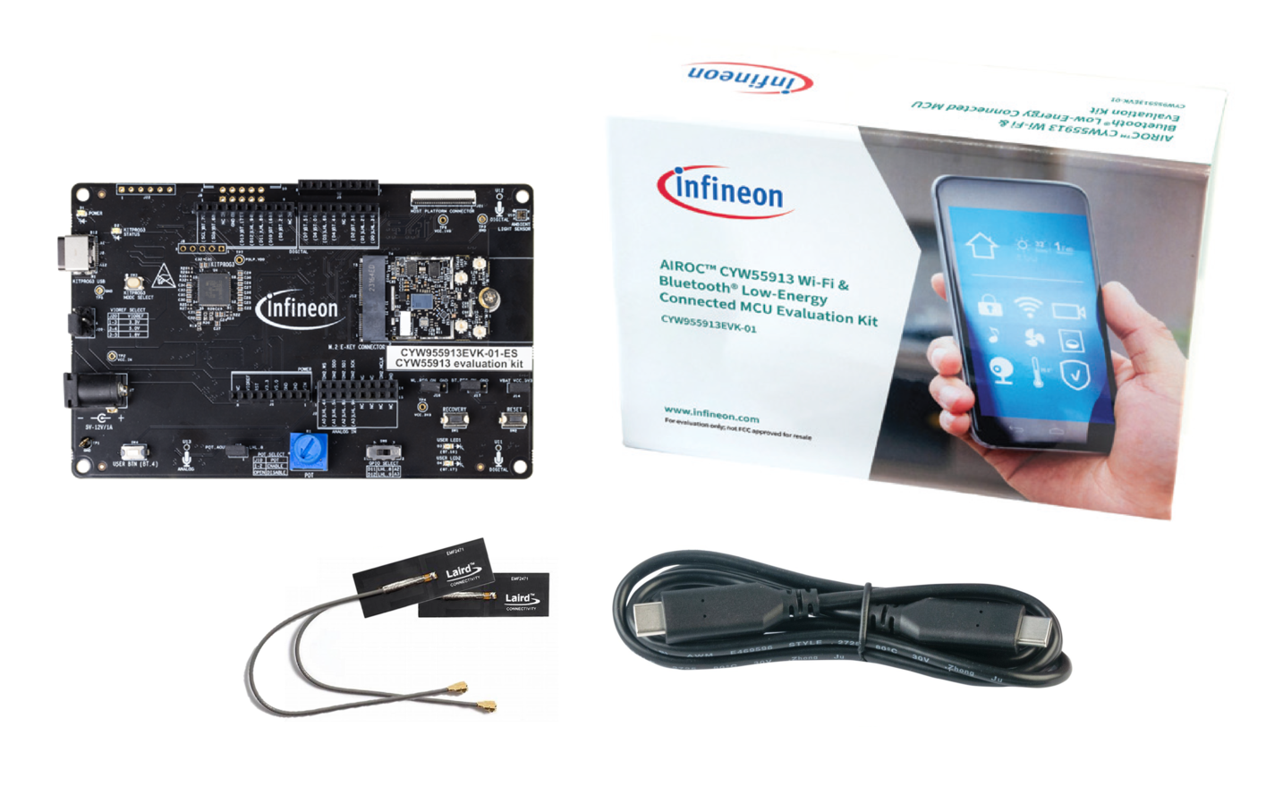
Figure 1 shows CYW955913EVK-01 kit contents. Inspect the kit contents. If you find any part missing, contact your nearest Infineon sales office for assistance: www.infineon.com/support.
Kit details
Figure 1 shows CYW955913EVK-01 with the following features:
- CYW55913 M.2 carrier module with antenna connectors
- Expansion headers compatible with Arduino shields
- Supports 1.8 V, 3.3 V, and 5 V operation of Arduino shields
- Reset button (black) and User button (white)
- Onboard USB Type-C connector (J6) for powering, programming, and debugging purposes
Follow these steps before connecting the board and verifying the driver installation:
- Verify that all the jumpers are in the default configuration, as shown in Table 3 to Table 6, so that the peripheral UART is selected and can display embedded application trace messages. Figure 2 shows the default jumper locations.
- Connect the USB connector (J6) of the EVK to the development PC with
the provided Type-C USB cable. The USB UART driver loads automatically. If the EVK
is not detected as a USB device, reinstall the USB UART driver in the following ModusToolbox™ installation directory:
- Windows and macOS: <install>\tools_3.2\driver_media\dpinst
- Linux: <install>\tools_3.2 \driver_media\install_driver\dpinst
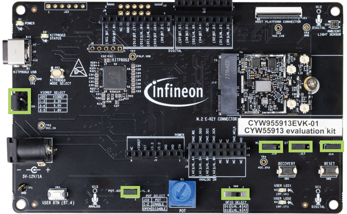
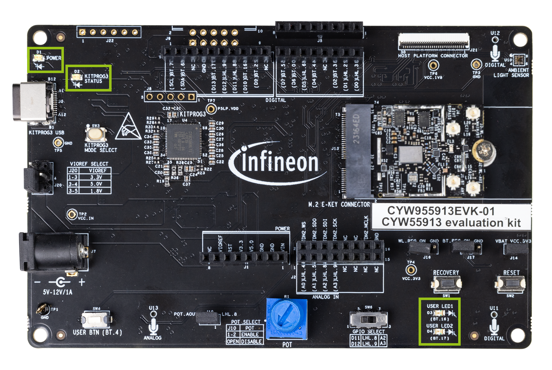
Figure 3 highlights the LEDs provided on CYW955913EVK-01:
- LED D1 (Yellow) indicates that input power is ON.
- LED D2 (Yellow) indicates KitProg3 status.
- LED D3 (Red) and LED D4 (Orange) are generic user LEDs controlled by GPIOs. A label on the back of the kit provides the pin mapping.
Getting started
This user guide helps you find the details of the CYW955913EVK-01 kit:
- The Kit operation chapter describes the operation of the kit and the utility of its various features.
- The Hardware chapter describes the design details of the CYW955913EVK-01 hardware blocks.
Perform the following steps to get started with the out of the box experience of the CYW955913EVK-01 Kit.
- Before you start, ensure that you have the following:
- PC with Type-C USB port
- UART terminal soft¬ware such as TeraTerm or Minicom
- Connect the Triband PCB antenna to the UFL connectors J3 (WL Main) and J2 (WL AUX) on the M.2 radio card
- Ensure that the jumper and switch settings on the board are configured as shown in Table 2 to Table 7
- Connect the KitProg3 USB Type-C connector (J6) to your PC
- Wait for the driver installation to complete
Figure 4. CYW955913EVK-01 Antenna connection 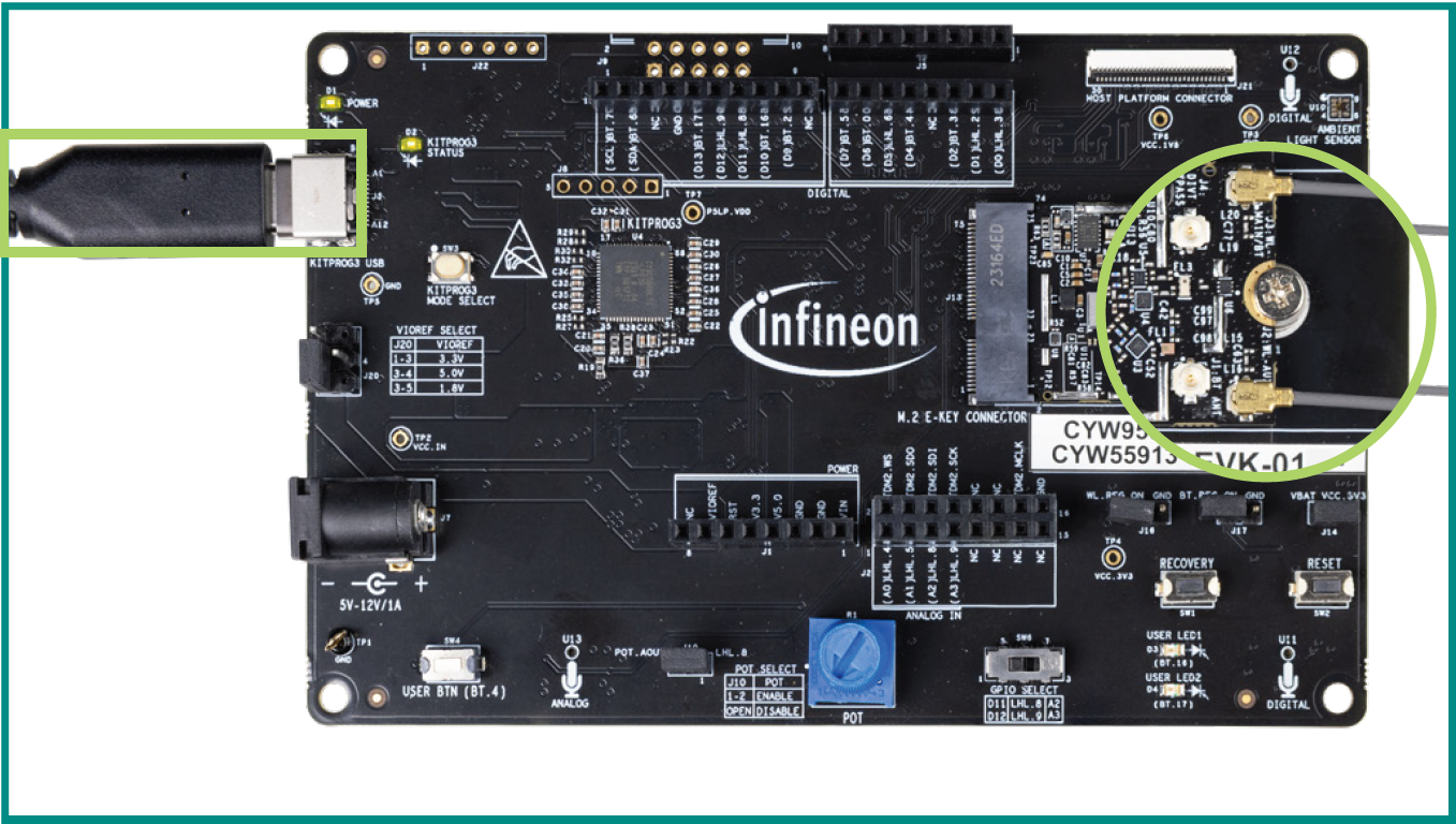
- Open the UART terminal software and connect to the kit’s Peripheral UART COM port with the
following settings:
- Baud rate: 115200
- Data: 8 bit
- Parity: None
- Stop bit: 1 bit
- Flow control: None
- Press the Reset button (SW2) and follow the instructions displayed on the UART terminal to use the pre-programmed code example
Figure 5. USB-UART COM port setup 
ModusToolbox™ software
ModusToolbox™ is a free software development ecosystem that includes the Eclipse IDE for ModusToolbox™, AIROC™ BTSTACK, Bluetooth® SDK, and Wi-Fi SDK to develop applications for Infineon IoT products. Eclipse IDE for ModusToolbox™ is a multi-platform, integrated development environment (IDE) used to create new applications, update application code, change middleware settings, and program or debug applications.
Using ModusToolbox™, you can enable and configure device resources and middleware libraries, write C source code, and program and debug the device. The build system infrastructure includes the new project creation wizard that can run independently of the Eclipse IDE, the make infrastructure, and other tools. This means you can choose your compiler, RTOS, and ecosystem without compromising usability or access to our industry-leading AIROC™ Wi-Fi and Bluetooth®, CAPSENSE™ Human Machine Interface (HMI), security, and various other features.
For more details on ModusToolbox™ installation and usage, see the Eclipse IDE for ModusToolbox™ user guide.
ModusToolbox™ code examples
This section provides information about the code examples available for the CYW55913 devices.
The code examples are part of ModusToolbox™ 3.2 version (or later) and are located under the BSP CYW955913EVK-01.
To create a project using ModusToolbox™, see Getting Started with Bluetooth® LE on AIROC™ CYW55913 and Getting Started with Wi-Fi on AIROC™ CYW55913 application notes for Bluetooth® and Wi-Fi applications development, respectively.
ModusToolbox™ help
Launch ModusToolbox™ and navigate to the following items for help documentation:
- Quick Start Guide: Choose Help > Eclipse IDE for ModusToolbox™ Documentation > Quick Start Guide. This guide gives you the basics of using ModusToolbox™.
- ModusToolbox™ General Documentation: Choose Help > ModusToolbox™ General Documentation > ModusToolbox™ Documentation Index. This page provides links to various ModusToolbox™ documents.
- ModusToolbox™ User Guide: Choose Help > Eclipse IDE for ModusToolbox™ Documentation > User Guide. This is a comprehensive guide for creating, building, and programming ModusToolbox™ applications.
Update programmer serial number for CYW55913
Programming an application onto a CYW55913 device is done through the UART interface. If there are two or more serial ports connected to your computer, add "UART=COMXX" (or "UART=/dev/ttyXX" for Linux or macOS) to the application Makefile. Replace XX with the appropriate UART number that is attached to the kit. For example:
UART=COM16
IoT resources and technical support
Infineon provides a wealth of product documentation at the Wireless Connectivity webpage to help you select the right IoT device for your design. Additionally, Infineon Developer Community offers a platform for developers to access the latest software and tools, solving common evaluation and integration problems while directly interacting with both Infineon engineers and experienced peers.
Kit operation
This section provides detailed instructions to setup the Infineon CYW955913EVK-01 with Infineon ModusToolbox™ for Wi-Fi and Bluetooth® LE combo applications with a connected MCU. It introduces CYW955913EVK-01 and the features that are used as part of the kit's operation. Also, discusses the features such as Wi-Fi and Bluetooth® connectivity, MCU capabilities, programming/debugging, and a USB-UART bridge device that can be used to communicate with the CYW55913 device on this EVK.
Theory of operation
CYW955913EVK-01 is built around the CYW55913 device. Figure 6 shows the block diagram of the CYW55913 device. See the device datasheet for more details on device features.
Figure 7 illustrates the block diagram of CYW955913EVK-01. This board contains a CYW55913 Wi-Fi and Bluetooth® LE-connected MCU and a USB-to-serial interface/programmer. The kit features Arduino form-factor-compatible headers, which enable Arduino shields to be plugged in, extending the EVK's capabilities. It also features one user button, a recovery button, a reset button, two user LEDs, a potentiometer, an ambient light sensor, an AMIC, and two DMICs.
Figure 8 and Figure 9 show the markup of the CYW955913EVK-01.
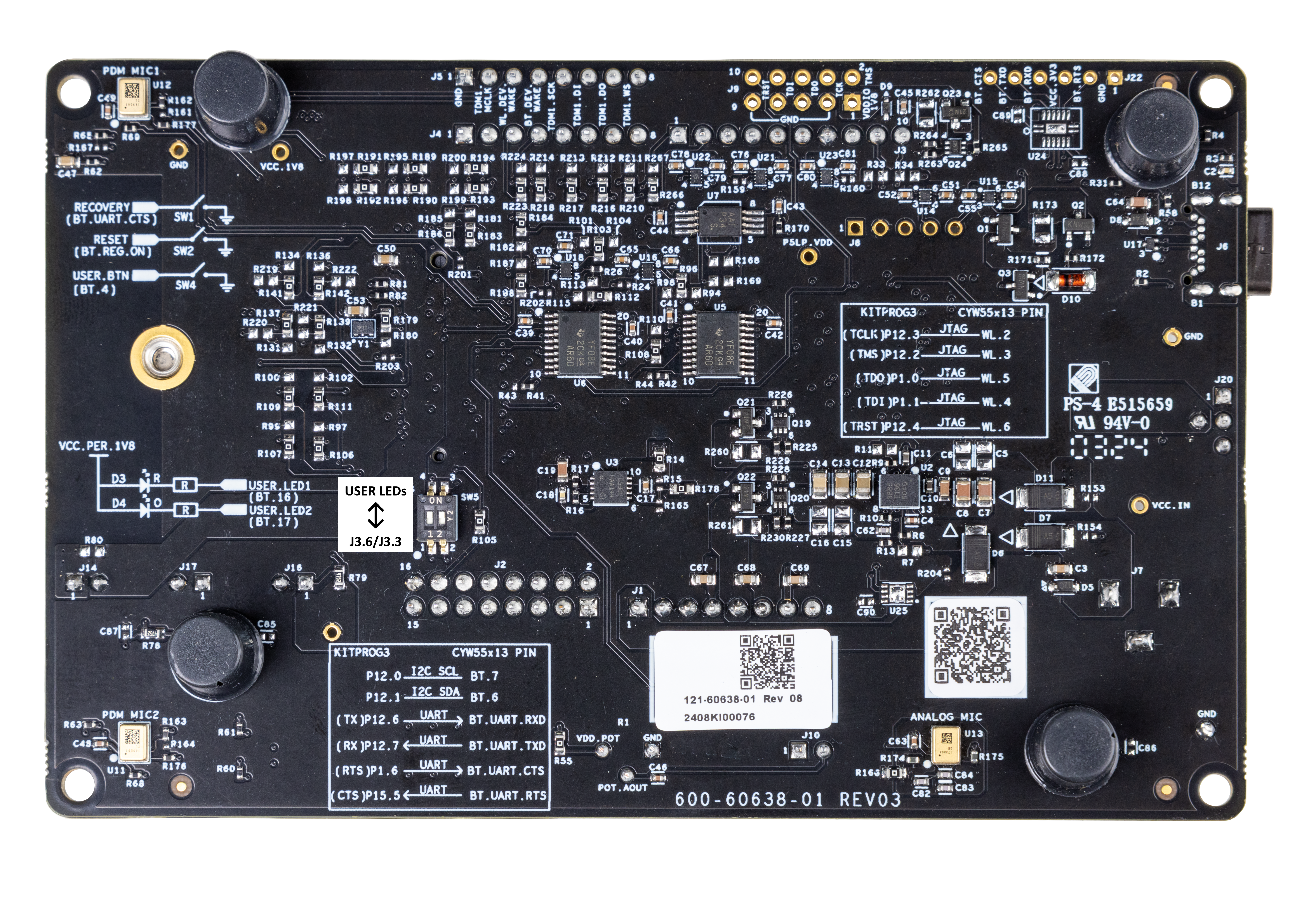
The following are the descriptions of the numbered items in Figure 8:
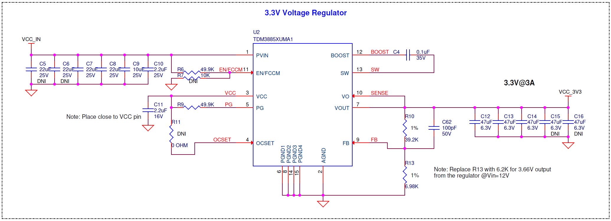
- Power indicator LED (D1): This LED is used to indicate the status of power supplied to the board.
- KitProg3 status LED (D2): This yellow LED indicates the status of KitProg3.
- KitProg3 USB Type-C connector (J6): J6 is a Type-C USB female connector for connecting the kit to the PC using the provided USB Type-C cable. It is used for powering the board, programming, and USB-UART communication.
- KitProg3 programming mode selection button (SW3): In this kit, by default, it supports Dual-UART mode. The button connects the PSOC™ 5LP Mode select pin to the ground when pressed. To interchange between Single-UART and Dual-UART mode, press and hold SW3 for 2 seconds. For more details, refer to the KitProg3 user guide.
- KitProg3 (PSOC™ 5LP) programmer and debugger (CY8C5868LTI-LP039, U4): The PSOC™ 5LP (CY8C5868LTI-LP039) serving as KitProg3, is a multi-functional system that includes a JTAG debugger, a USB-I2C bridge, and a Dual USB-to-UART bridge. For more details, see the KitProg3 user guide.
- VIOREF voltage selection jumper (J20): This jumper is used to select the VIOREF (Arduino shield IO supply) power source. The possible selections are 1.8 V, 3.3 V, or 5.0 V.
- External power supply VIN connector (J7): This is an optional power supply DC jack that support 12 V and 1 A to power the board.
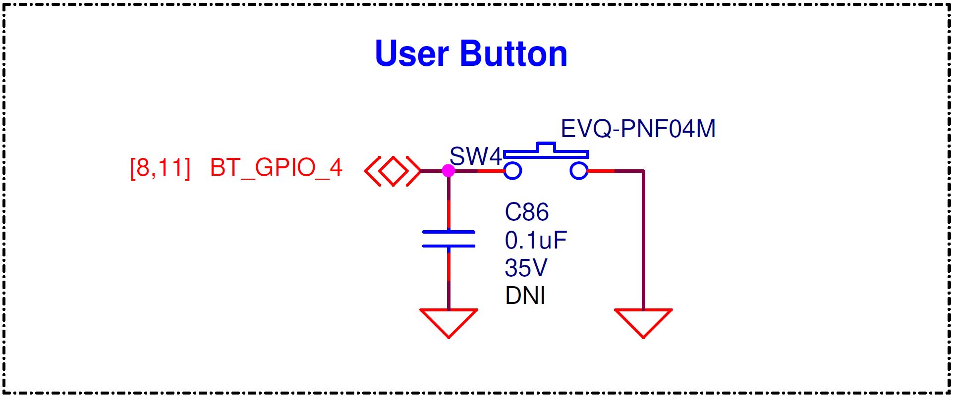
- CYW55913 user button (SW4): This button can be used to provide input to the CYW55913 device. Note that the button connects the CYW55913 pin to the ground when pressed; therefore, the CYW55913 pin must be configured as a digital input with a resistive pull-up for detecting the button press.
- LED enable/disable switch (SW5): This switch is used to enable or disable the user LEDs by connecting or disconnecting GPIOs from CYW55913.
- Analog mic (U13): It can be used to configure the kit as a voice remote.
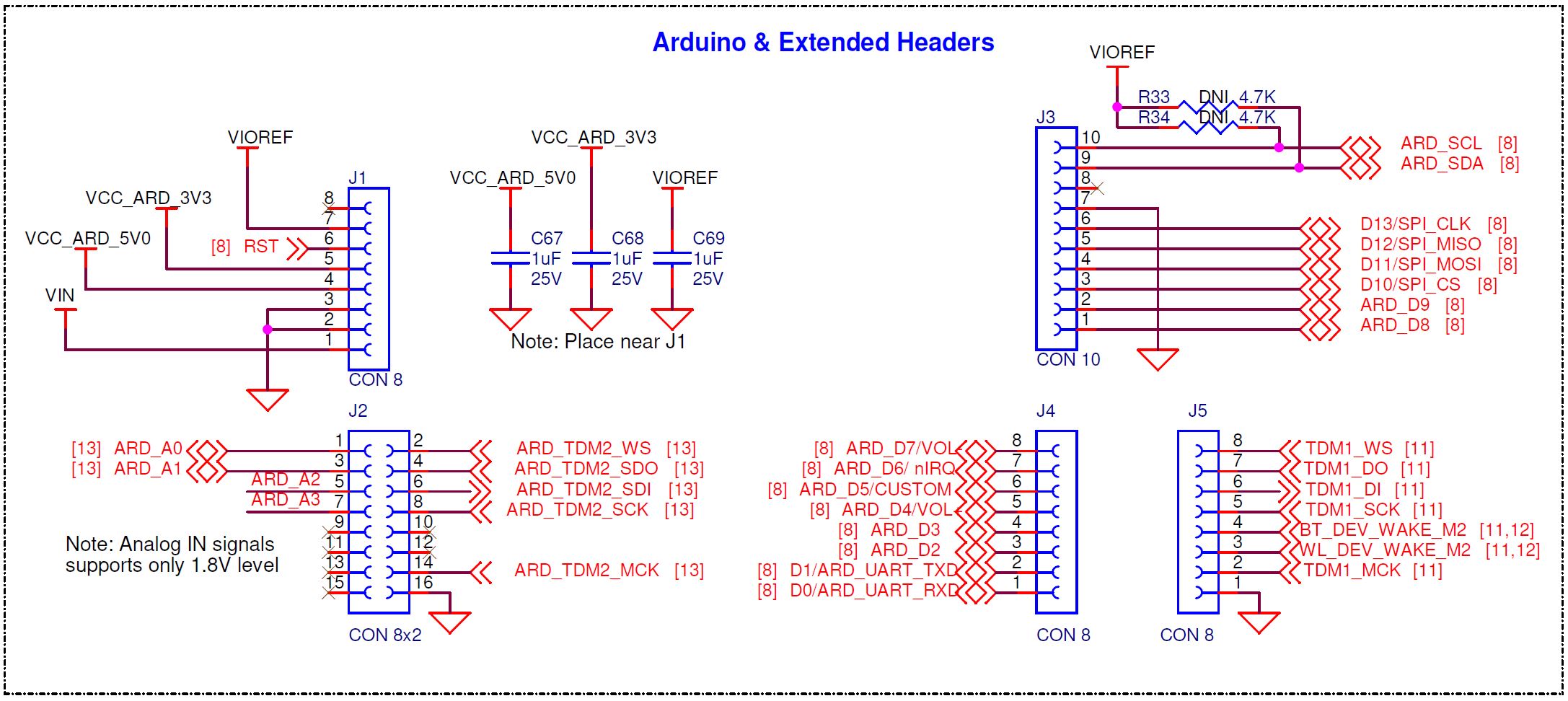
- Power header compatible with Arduino Uno R3 (J1): The Arduino-compatible I/O header brings out power and reference voltage pins from the base board to interface with Arduino shields.
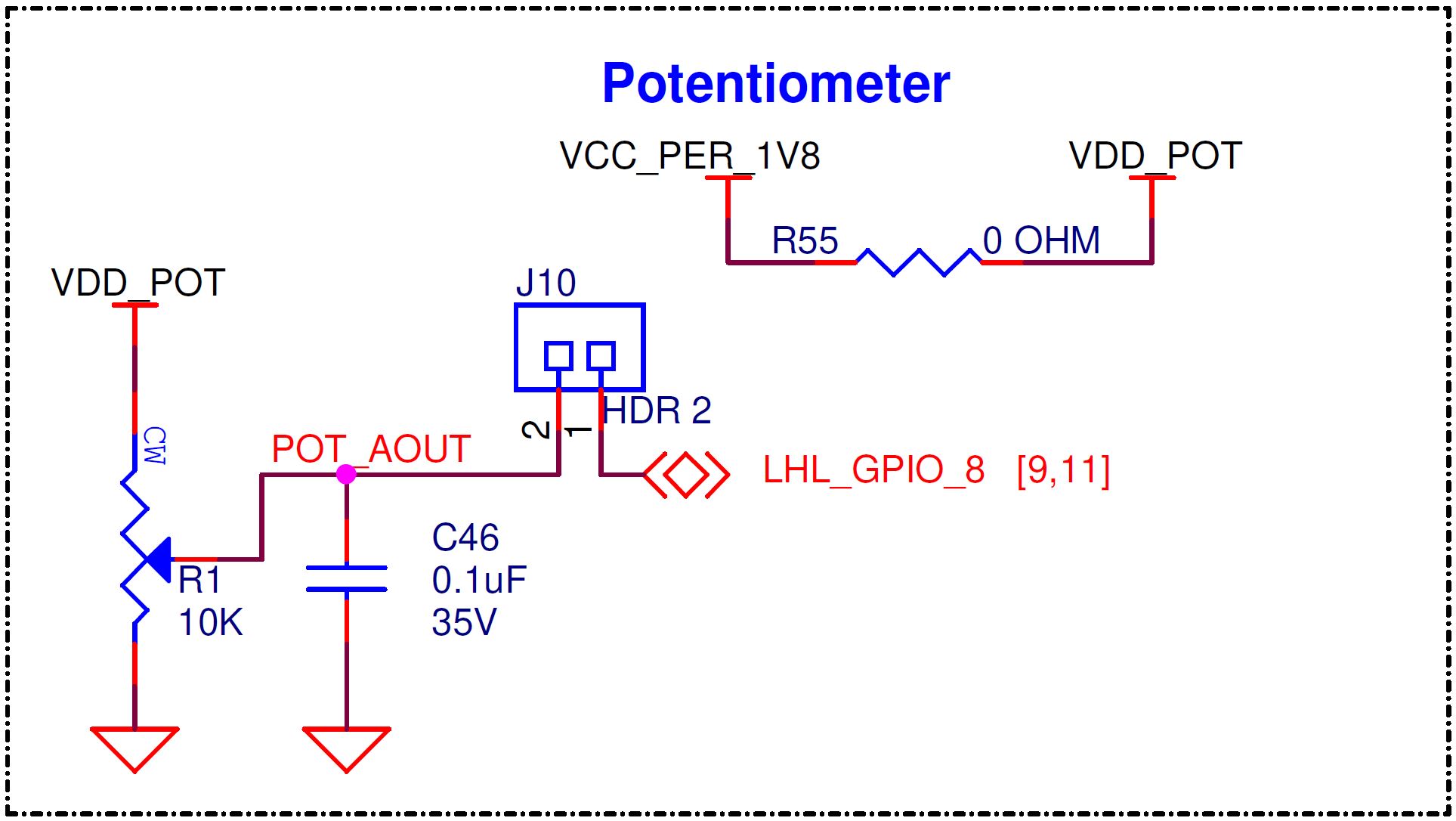
- Potentiometer connection jumper (J10): This jumper can be used to connect or disconnect the on-board potentiometer from the CYW55913 device.
- Potentiometer (R1): This enables the kit to demonstrate the analog input capability of the CYW55913 chip.
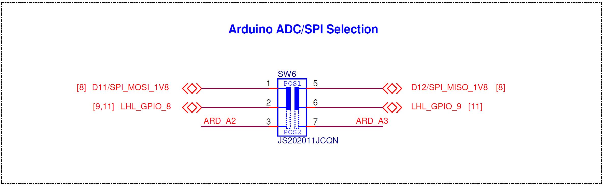
- Arduino ADC/SPI selection switch: This DPDT switch is used to select between the connection of GPIO from CYW55913 to Arduino headers.
- Analog-IN header compatible with Arduino Uno R3 with Extended TDM2 interface (J2): The Arduino-compatible I/O header brings out analog-capable pins and Audio TDM2 interface from CYW55913 to interface with Arduino shields.
- CYW55913 user LEDs (D3, D4): These onboard LEDs can be controlled by the CYW55913 device. The LEDs are ACTIVE LOW; therefore, these pins must be driven low to turn ON the LEDs.
- Digital mic 1 (U11): The digital microphone ASIC contains an extremely low-noise preamplifier and a high-performance sigma-delta ADC. It can be used to configure the kit as a voice remote.
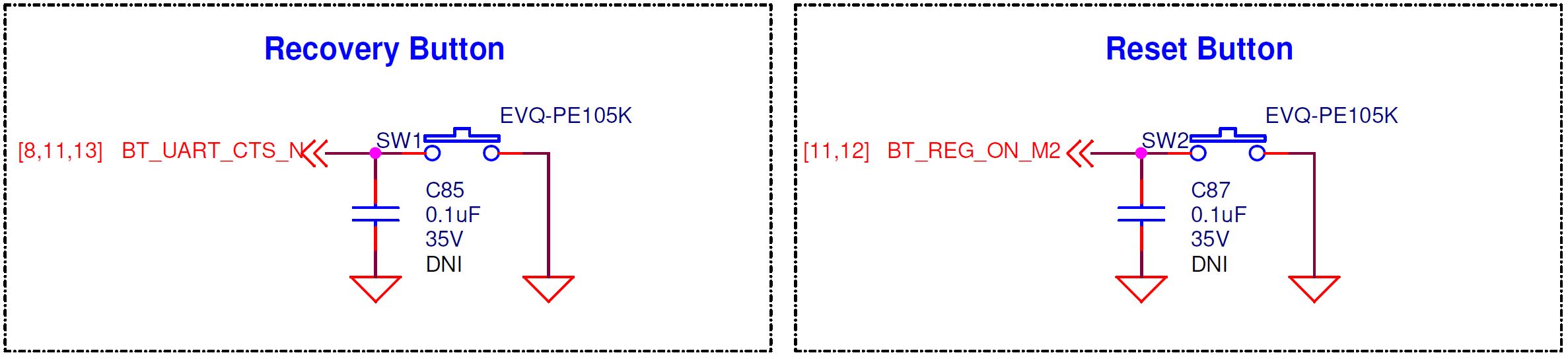
- CYW55913 reset button (SW2): This button can be used to reset the device.
- CYW55913 recovery button (SW1): This button can be used to force the device to recovery mode.
- VBAT current measurement jumper (J14): This jumper is used to power the M.2 carrier module. Remove this jumper and connect an ammeter across the two pins of J14 to measure the current consumption by the M.2 carrier module.
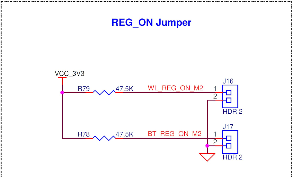
- Bluetooth® section disable jumper (J17): This jumper is used to enable/disable BT subsystem of the device.
- WLAN section disable jumper (J16): This jumper is used to enable/disable WLAN subsystem of the device.
- M.2 stand-off (MT1): Stand-off to connect the M.2 carrier module.
- CYW55913 (U1): AIROC™ Wi-Fi and Bluetooth® LE connected MCU with Wi-Fi 6 and Bluetooth® LE 5.4 support is the heart of the kit.
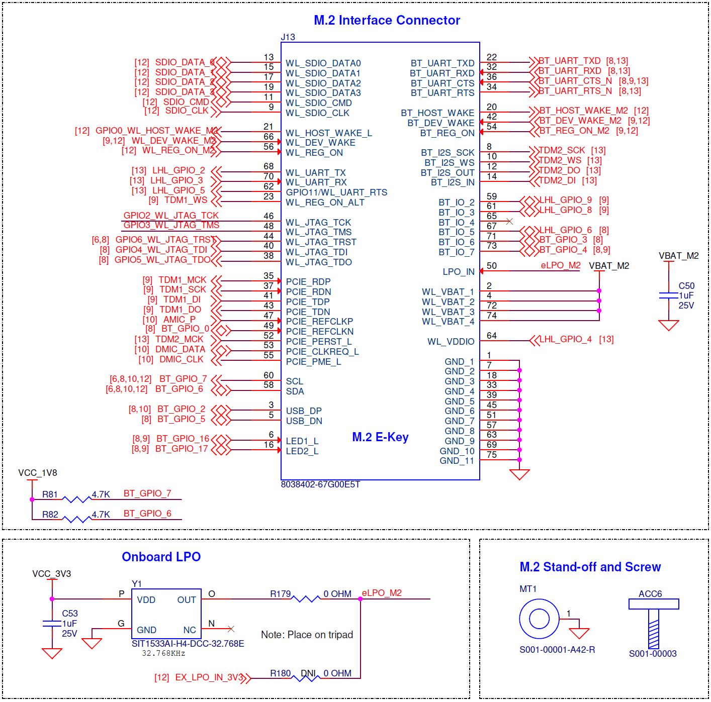
- M.2 E-key interface connector (J13): This is used to interface Infineon custom Wi-Fi and Bluetooth® LE connected MCU M.2 carrier boards to this kit.
- Ambient light sensor (U10): On-board digital ambient light sensor can be used to sense the ambient light intensity and provide the data to the CYW55913 device via I2C.
- Digital mic 2 (U12): Second digital PDM mic on board enables the stereo audio input functionality.
- External host platform interface connector (J21): This 30-pin connector enables the CYW55913 device to connect to other host platforms.
- TDM1 interface connector (J5): This connector exposes the audio TDM1 interface of the CYW55913 device.
- Digital I/O headers compatible with Arduino Uno R3 (J3, J4): The Arduino-compatible I/O header brings out pins from CYW55913 to interface with Arduino shields.
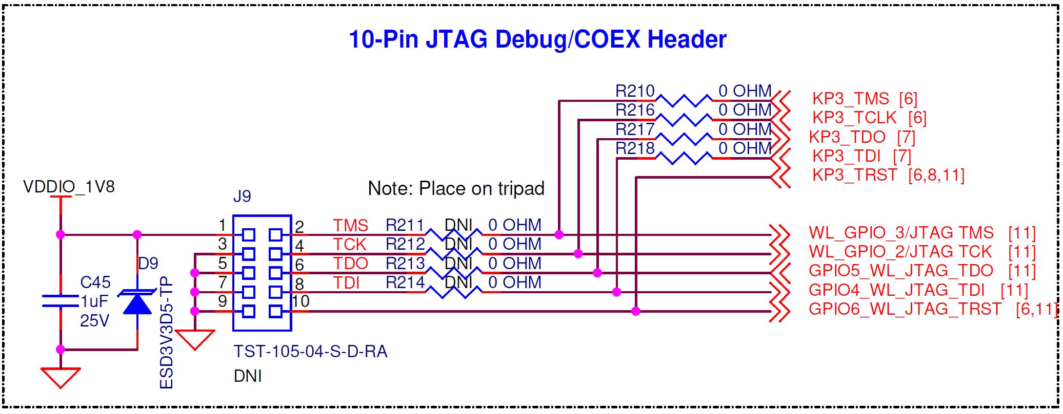
- 10-pin JTAG/COEX header (J9): Optional (not mounted) header to access the JTAG/COEX interface of the device.
- 6-pin Bluetooth® UART header (J22): Optional (not mounted) header to access BT UART interface of the device.
Jumpers
Table 2 to Table 6 list the jumper settings on the CYW955913EVK-01.
| Baseboard Jumper J14 (VBAT current measurement) | Default state | Connection on CYW55913 | Description |
|---|---|---|---|
| 1 and 2 | Shorted | VBAT | Short this jumper to supply power to the VBAT of CYW55913. In addition, use this jumper to measure the current consumption of the VBAT domain. |
| Baseboard jumper J16 (WLAN Disable) | Default state | Connection on CYW55913 | Description |
|---|---|---|---|
| 1 and 2 | Open | NA | Short this jumper to disable the WLAN section of
the radio module on the M.2 carrier board. Note: This jumper
can be used for radio modules other than CYW55913 as WL_REG_ON is not
exposed on this device. |
| Baseboard jumper J17 (BT Disable) | Default state | Connection on CYW55913 | Description |
|---|---|---|---|
| 1 and 2 | Open | REG_ON | Short this jumper to disable the BT subsystem of the CYW55913 device. Note: Shorting
this jumper disables both the BT and WL subsystem on the CYW55913
device, as both Reg_ON pins are tied together. |
| Baseboard jumper J10 (Potentiometer enable) | Default state | Connection on CYW55913 | Description |
|---|---|---|---|
| 1 and 2 | 1-2 |
LHL_GPIO_8 | Short this jumper to connect the onboard potentiometer to CYW55913. |
| Baseboard jumper J20 (Arduino header VIOREF select) | Default state | Connection on CYW55913 | Description |
|---|---|---|---|
| 1 and 3 | Open | NA | Short these pins to supply 3.3 V to the VIOREF of the Arduino header. |
| 3 and 4 | Open | Short these pins to supply 5.0 V to the VIOREF of the Arduino header. | |
| 3 and 5 | Shorted | Short these pins to supply 1.8 V to the VIOREF of the Arduino header. |
Buttons and switches
Table 7 lists the buttons and switches on the CYW955913EVK-01.
| Baseboard buttons/switch | Pressed state | Connection on CYW55913 | Description |
|---|---|---|---|
| SW1 | GND | BT_UART_CTS | Active low recovery button (black) |
| SW2 | GND | BT_REG_ON | Active low reset button (black) |
| SW3 | GND | NA | Switch to change the KP3 mode |
| SW4 | GND | BT_GPIO_4 | User application button (white) |
| SW5 | NA | BT_GPIO_16 BT_GPIO_17 |
User LED1 and User LED2 enable/disable switch |
| SW6 | NA | LHL_GPIO_8 LHL_GPIO_9 |
Arduino GPIO ADC/SPI selection switch |
Arduino-compatible headers
J1, J2, J3, J4, and J5 are Arduino shield-compatible headers.
| Header J1 | Arduino compatible pin | Connection on CYW55913 | Description |
|---|---|---|---|
| 1 | VIN | NA | Input supply (5 V - 12 V) option to the kit from the Arduino shield |
| 2 | GND | GND | Ground |
| 3 | GND | GND | Ground |
| 4 | 5V0 | NA | 5 V supply output to the Arduino shield |
| 5 | 3V3 | NA | 3.3 V supply output to the Arduino shield |
| 6 | RESET | NA | Arduino shield reset from KP3 |
| 7 | VIOREF | NA | I/O reference pin used by shields to determine the I/O voltage. It can be changed to 1.8 V, 3.3 V, and 5 V with J20 configuration. |
| 8 | NC | NC | No connect |
| Header J2 | Arduino compatible pin | Connection on CYW55913 | Description |
|---|---|---|---|
| 1 | A0 | LHL_GPIO_4 | LHL GPIO |
| 2 | NA | TDM2_WS | TDM2 interface word select |
| 3 | A1 | LHL_GPIO_5 | LHL GPIO |
| 4 | NA | TDM2_SDO | TDM2 interface data out |
| 5 | A2 | LHL_GPIO_8 | LHL GPIO |
| 6 | NA | TDM2_SDI | TDM2 interface data in |
| 7 | A3 | LHL_GPIO_9 | LHL GPIO |
| 8 | NA | TDM2_SCK | TDM2 interface slave clock |
| 9 | NC | NA | No connect |
| 10 | NC | NA | No connect |
| 11 | NC | NA | No connect |
| 12 | NC | NA | No connect |
| 13 | NC | NA | No connect |
| 14 | NA | TDM2_MCK | TDM2 interface master clock |
| 15 | NC | NA | No connect |
| 16 | GND | GND | Ground |
| Header J3 | Arduino compatible pin | Connection on CYW55913 | Description |
|---|---|---|---|
| 1 | D8 | NC | No Connect |
| 2 | D9 | BT_GPIO_2 | BT GPIO |
| 3 | D10 | BT_GPIO_16 | BT_GPIO |
| 4 | D11 | LHL_GPIO_8 | LHL GPIO |
| 5 | D12 | LHL_GPIO_9 | LHL GPIO |
| 6 | D13 | BT_GPIO_17 | BT GPIO |
| 7 | GND | GND | Ground |
| 8 | NC | NC | No connect |
| 9 | SDA | BT_GPIO_6 | BT GPIO |
| 10 | SCL | BT_GPIO_7 | BT GPIO |
| Header J4 | Arduino compatible pin | Connection on CYW55913 | Description |
|---|---|---|---|
| 1 | D0 | LHL_GPIO_3 | LHL GPIO |
| 2 | D1 | LHL_GPIO_2 | LHL GPIO |
| 3 | D2 | BT_GPIO_3 | BT GPIO |
| 4 | D3 | NC | No connect |
| 5 | D4 | BT_GPIO_4 | BT GPIO |
| 6 | D5 | LHL_GPIO_6 | LHL_GPIO |
| 7 | D6 | BT_GPIO_0 | BT GPIO |
| 8 | D7 | BT_GPIO_5 | BT GPIO |
| Header J5 | Arduino compatible pin | Connection on CYW55913 | Description |
|---|---|---|---|
| 1 | NA | GND | Ground |
| 2 | NA | TDM1_MCK | TDM1 interface master clock |
| 3 | NA | WL_DEV_WAKE | WLAN device wake |
| 4 | NA | BT_DEV_WAKE | Bluetooth® device wake |
| 5 | NA | TDM1_SCK | TDM1 interface slave clock |
| 6 | NA | TDM1_DI | TDM1 interface data in |
| 7 | NA | TDM1_DO | TDM1 interface data out |
| 8 | NA | TDM1_WS | TDM1 interface word select |
Other headers
J9 is the JTAG/COEX header, which brings out the WL GPIOs of the CYW55913 device (not mounted by default; see the Kit reworks chapter for use).
| Header J9 | Pin name | Connection on CYW55913 | Description |
|---|---|---|---|
| 1 | VDDIO_1V8 | NA | 1.8 V supply to the external debugger |
| 2 | TMS | GPIO_3 | WL GPIO |
| 3 | GND | GND | Ground |
| 4 | TCK | GPIO_2 | WL GPIO |
| 5 | GND | GND | Ground |
| 6 | TDO | GPIO_5 | WL GPIO |
| 7 | GND | GND | Ground |
| 8 | TDI | GPIO_4 | WL GPIO |
| 9 | GND | GND | Ground |
| 10 | TRST | GPIO_6 | WL GPIO |
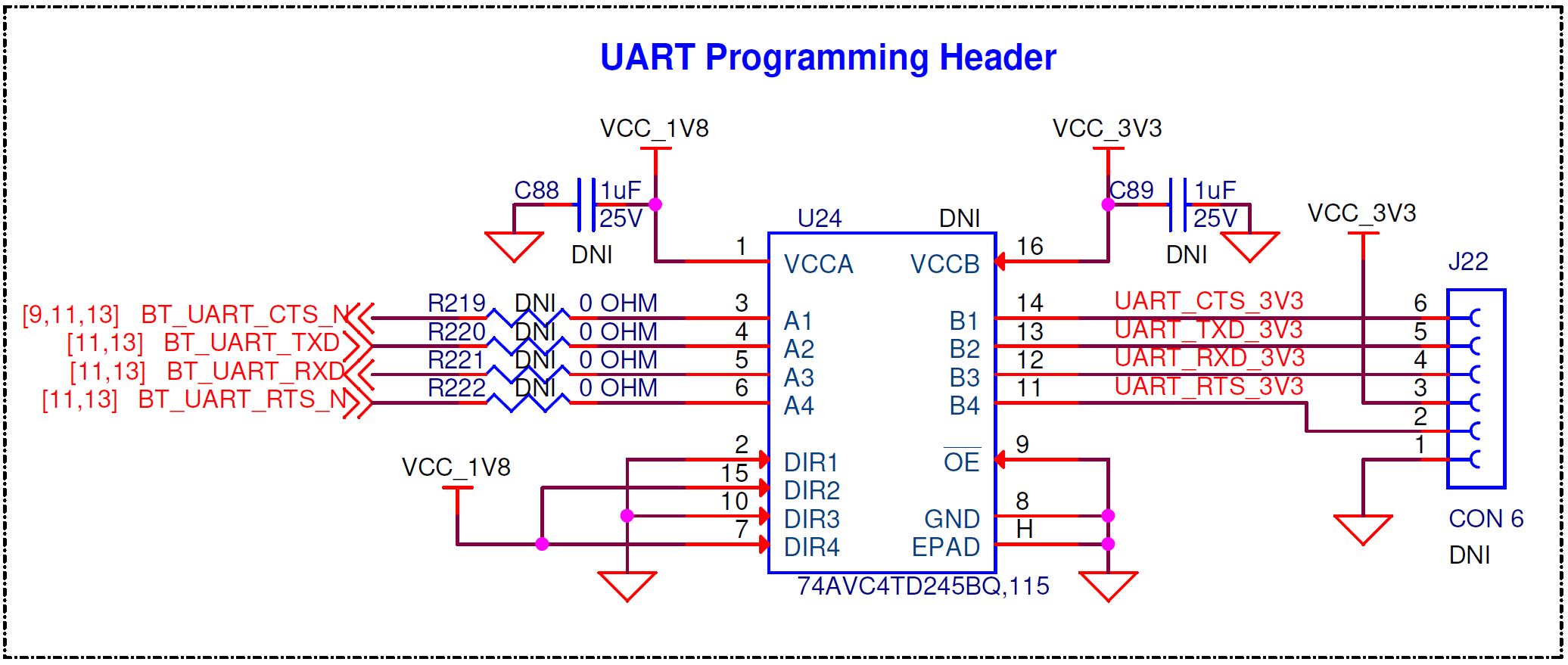
J22 is a UART programming header using an external device that brings out the HCI UART pins of the CYW55913 device (not mounted by default; see the Kit reworks chapter for use).
| Header J22 | Pin name | Connection on CYW55913 | Description |
|---|---|---|---|
| 1 | GND | GND | Ground |
| 2 | UART_RTS | BT_UART_RTS_N |
UART request-to-send. Active-low request-to-send signal for the HCI UART interface. |
| 3 | VCC_3V3 | NA | 3.3 V supply |
| 4 | UART_RXD | BT_UART_RXD |
UART serial input. Serial data input for the HCI UART interface. |
| 5 | UART_TXD | BT_UART_TXD |
UART serial output. Serial data output for the HCI UART interface. |
| 6 | UART_CTS | BT_UART_CTS_N |
UART clear-to-send. Active-low clear-to-send signal for the HCI UART interface. |
| Header J21 | Pin name | Connection on CYW55913 | Description |
|---|---|---|---|
| 1 | EX_LHL_GPIO_3/UART_RXD | LHL_GPIO_3 | LHL GPIO |
| 2 | EX_LHL_GPIO_2/UART_TXD | LHL_GPIO_2 | LHL_GPIO |
| 3 | WL_DEV_WAKE_M2 | WL_DEV_WAKE | WLAN device wake |
| 4 | EX_LHL_GPIO_5/UART_RTS | LHL_GPIO_5 | LHL GPIO |
| 5 | BT_GPIO_7 | BT_GPIO_7 | BT GPIO |
| 6 | BT_GPIO_6 | BT_GPIO_6 | BT GPIO |
| 7 | WL_REG_ON_M2 | WL_REG_ON | Enable it for WLAN section power supply. Not used in the CYW55913 device, connected to GND on the device side. |
| 8 | BT_REG_ON_M2 | BT_REG_ON |
Used by the PMU to power on or power off the internal CYW55913 regulators used by the Bluetooth® section. |
| 9 | EX_LPO_IN_3V3 | LPO_IN_OUT | LPO clock input from external host board |
| 10 | BT_DEV_WAKE_M2 | BT_DEV_WAKE | Bluetooth® device wake |
| 11 | GND | GND | Ground |
| 12 | EX_BT_UART_CTS | BT_UART_CTS_N |
UART clear-to-send. Active-low clear-to-send signal for the HCI UART interface. |
| 13 | EX_BT_UART_RTS | BT_UART_RTS_N |
UART request-to-send. Active-low request-to-send signal for the HCI UART interface. |
| 14 | EX_BT_UART_RXD | BT_UART_RXD |
UART serial input. Serial data input for the HCI UART interface. |
| 15 | EX_BT_UART_TXD | BT_UART_TXD |
UART serial output. Serial data output for the HCI UART interface. |
| 16 | GND | GND | Ground |
| 17 | BT_HOST_WAKE_M2 | BT_HOST_WAKE | Bluetooth® host wake |
| 18 | GPIO0_WL_HOST_WAKE_M2 | GPIO_0 | WLAN host wake |
| 19 | GND | GND | Ground |
| 20 | EX_TDM2_DI | TDM2_DI | TDM2 interface data in |
| 21 | EX_TDM2_DO | TDM2_DO | TDM2 interface data out |
| 22 | EX_TDM2_WS | TDM2_WS | TDM2 interface word select |
| 23 | EX_TDM2_SCK | TDM2_SCK | TDM2 interface slave clock |
| 24 | GND | GND | Ground |
| 25 | EXT_SDIO_DATA3 | SDIO_DATA_3 | SDIO data line 3 |
| 26 | EXT_SDIO_DATA2 | SDIO_DATA_2 | SDIO data line 2 |
| 27 | EXT_SDIO_DATA1 | SDIO_DATA_1 | SDIO data line 1 |
| 28 | EXT_SDIO_DATA0 | SDIO_DATA_0 | SDIO data line 0 |
| 29 | EXT_SDIO_CMD | SDIO_CMD | SDIO command line |
| 30 | EXT_SDIO_CLK | SDIO_CLK | SDIO clock input |
USB serial interface chip
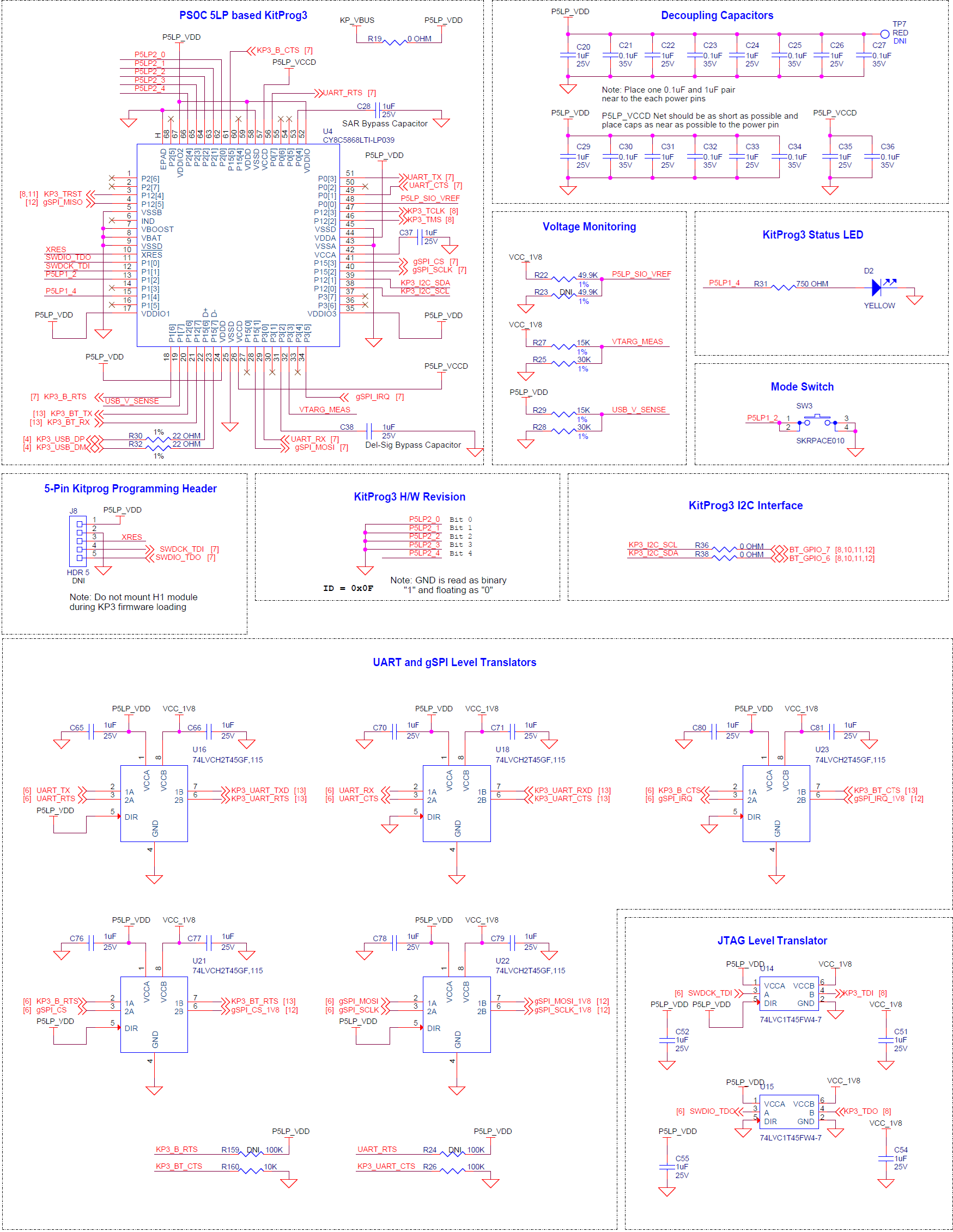
A CY8C5868LTI-LP039 PSOC™ 5LP chip is used for onboard programming and USB-serial functionality. It connects the kit to the PC over a USB interface and to the CYW55913 device through the HCI, peripheral UARTs, and I2C pins. Optional SPI and JTAG connectivity are also supported by this chip.
Kit power supply
The CYW955913EVK-01 kit can be powered with the following power inputs:
- USB Type-C connector (J6)
- 5 V - 12 V, 1 A DC jack (J7)
- VIN pin of the J1 header (J1.1)
The input supply is provided to the buck regulator to generate 3.3 V for the VBAT supply of the device, and from the same 3.3 V; for the peripherals, 1.8 V is generated using an LDO. For more details about the power regulators, see the Hardware section.
Test points
There are three ground test points for easy connection of probes. Table 16 lists voltage at various domains that can be measured from their respective test points on the baseboard.
| Label | Description |
|---|---|
| TP1, TP3, TP5 | Ground |
| TP2 | Input supply test point, VCC_IN |
| TP4 | 3.3 V rail test point, VCC_3V3 |
| TP6 | 1.8 V rail test point, VCC_1V8 |
| TP7 | P5LP supply test point, P5LP_VDD |
Current measurement
CYW955913EVK-01 has a VBAT (3.3 V) power domain to power the CYW55913 device. Current consumption of the M.2 carrier module with the CYW55913 device can be found out from the current consumed by the VBAT domain.
Pin configuration
GPIOs on the CYW55913 device can be multiplexed to various peripherals. For more information on the peripherals that can be routed to the various GPIOs; see the device datasheet.
Hardware
This section describes the CYW955913EVK-01 kit hardware and its different blocks, such as the power supply, reset control, Arduino-compatible headers, other connectors, and peripherals. This kit consists of two boards: a baseboard with all peripherals and interconnect options and an M.2 carrier module with the CYW55913 device .
See the CYW955913EVK-01 kit webpage for schematics and design files of the baseboard, and M.2 carrier module.
M.2 carrier module
The baseboard design of the CYW955913EVK-01 board is designed to be modular so that different carrier modules can be used with the same baseboard. In this kit, the CYW955913SCM2WLIPA M.2 carrier radio module, which employs the CYW55913 device, is connected to the baseboard through the M.2 interface.
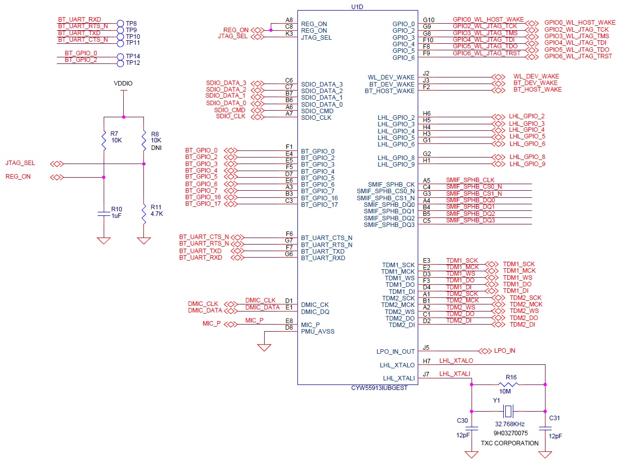
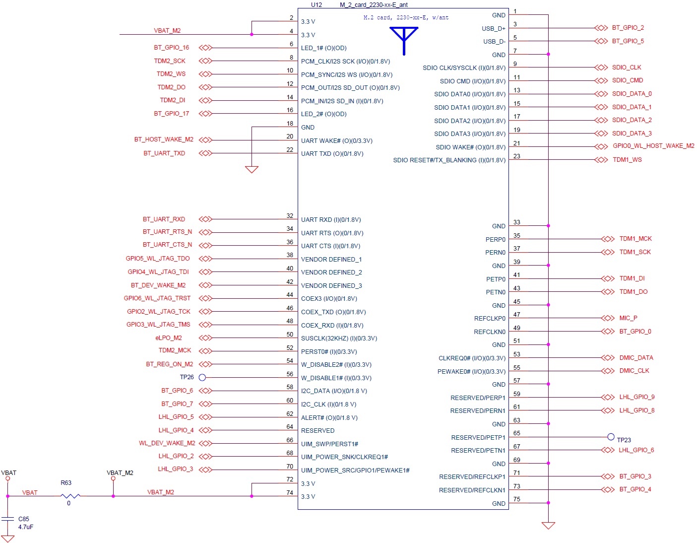
The carrier module interface is a generic interface used across many devices. See device I/O mapping for a detailed interface description. SDIO, UART signals, and GPIOs are moved out from module pins to interface with the baseboard.
CYW55913 device
CYW55913 is the heart of the kit, which is an ultra-low-power, single-chip, connected MCU that supports 1x1 Wi-Fi 6/6E, Bluetooth® LE 5.4, Matter, IP networking, with integrated PMU, targeted at Internet of Things (IoT) applications for standalone operation or to offload a host-processor.
An integrated 192 MHz Arm® Cortex®-CM33 runs the Wi-Fi and Networking Stacks, Bluetooth® LE 5.4, and supports a wide array of peripherals. The CYW55913/55912/55911/55903/55902/55901 operates over the -40°C to +85°C temperature range and is available in a 0.35 mm pitch WLBGA package.
CYW55913 device powered from VBAT 3.3 V and VDDIO 1.8 V. All sections are powered from the internally generated power outputs.
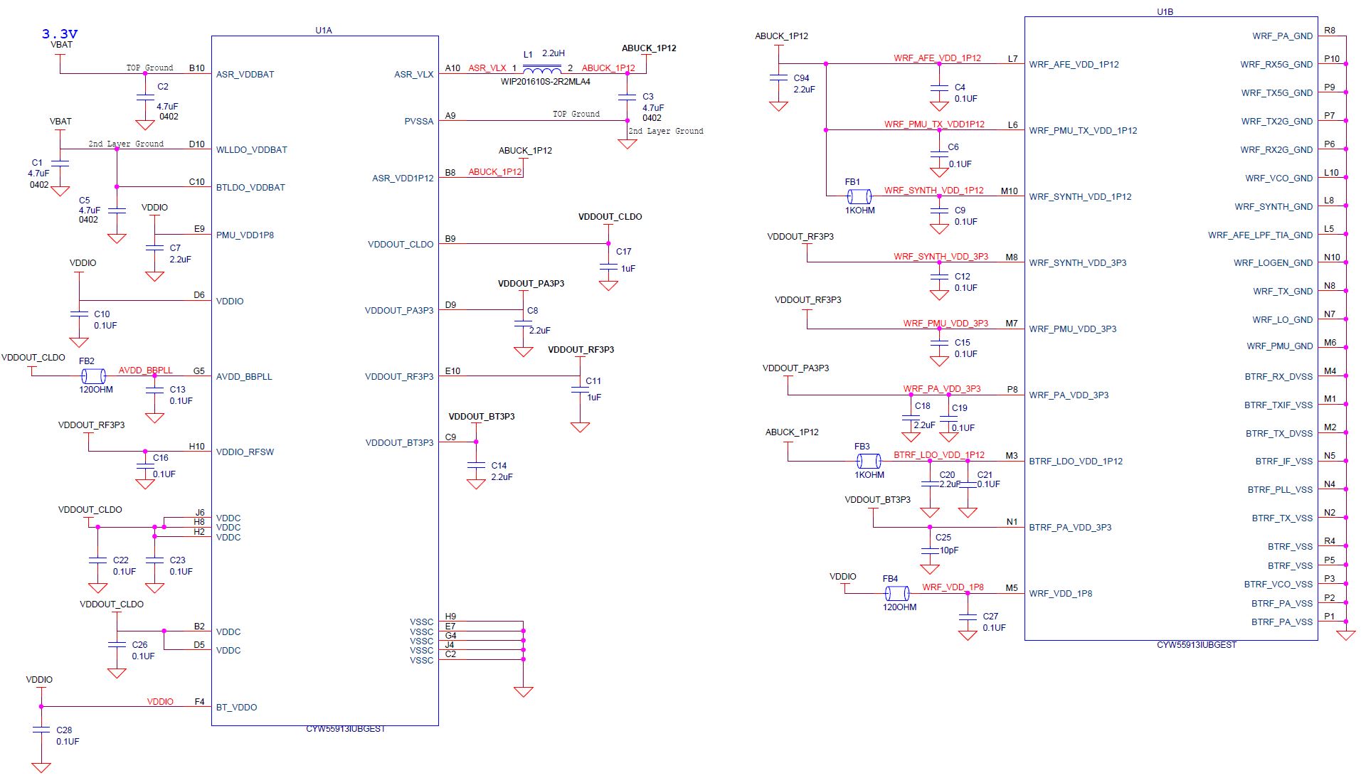
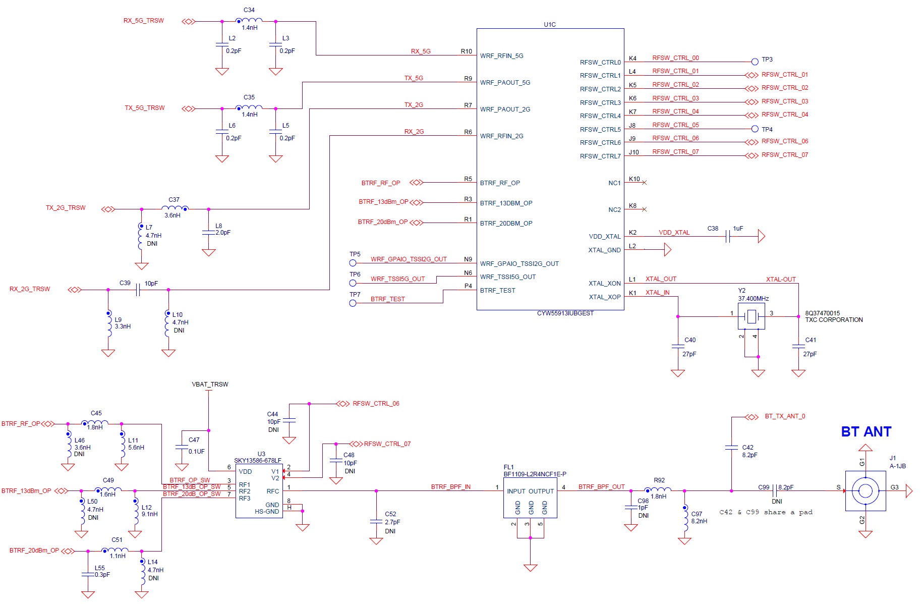
CYW55913 Carrier M.2 card also includes the RF front end for the Triband WiFi and BT. This section consists of RF switches, BPF and Matching networks that terminates to the UFL antenna connectors.
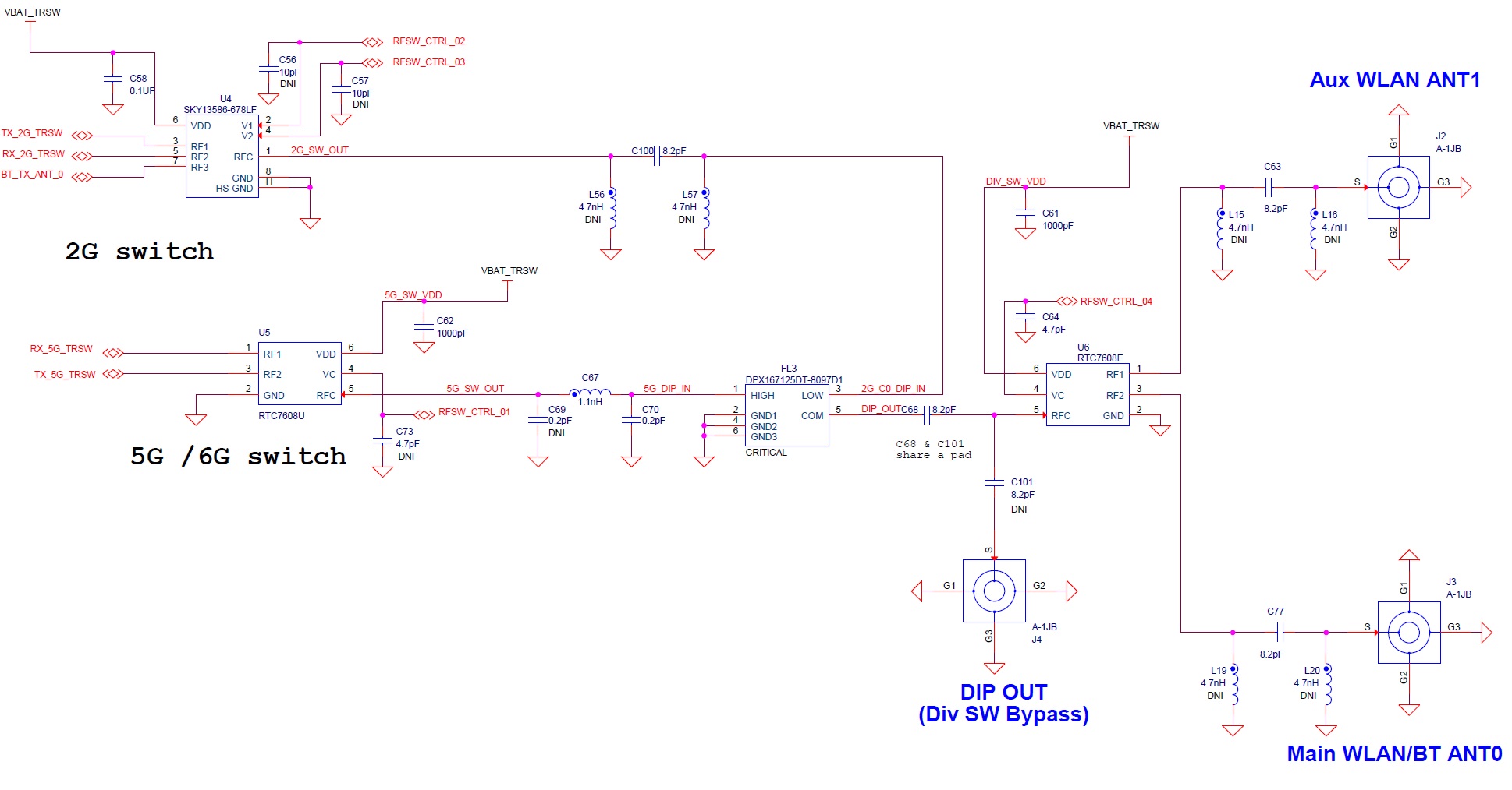
The M.2 Carrier Board is interfaced with the Baseboard via the M.2 E-Key standard edge finger connector.
Crystals
The CYW55913 M.2 carrier module has two crystals onboard, a 37.4 MHz crystal which provides the system reference clock and can operate from an internal high-accuracy (~1%) and a 32.768 kHz low-power oscillator (iLPO) or external 32.76 kHz crystal (eLPO) for higher accuracy or from an external reference clock.
Memory
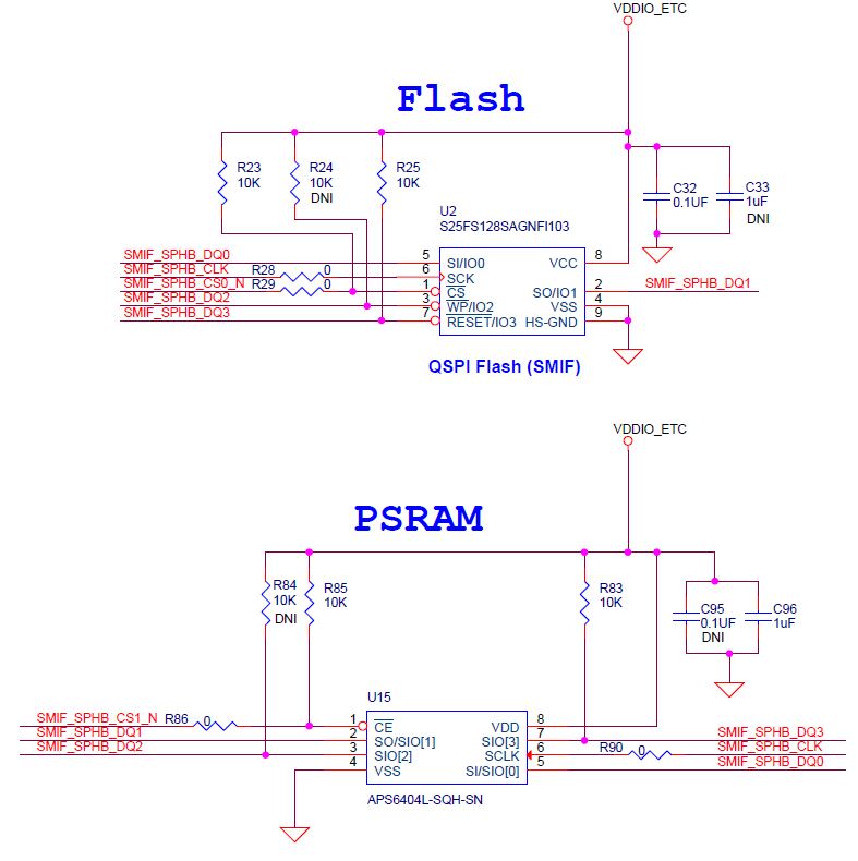
CYW955913SCM2WLIPA M.2 carrier module also includes external memory connected to the CYW55913 device via the SMIF interface. One QSPI flash is provided on the M.2 carrier board, which is interfaced with CYW55913 device through an SMIF interface with separate chip select.
Baseboard
CYW9CPM2BASE1 is the baseboard on which the CYW55913 M.2 carrier module (CYW955913SCM2WLIPA) is mounted. The baseboard is interfaced with the M.2 carrier module through the M.2 E-Key connector, and it provides different peripherals and extended connectors to demonstrate the capabilities of the CYW55913 device.
Serial communication between CYW55913 and PSOC™ 5LP KitProg3
The onboard CY8C5868LTI-LP039 PSOC™ 5LP device is a true programmable embedded system-on-chip responsible for two-channel USB-serial conversion on this baseboard. The USB-serial pins of the PSOC™ 5LP device are hard-wired to the HCI UART pins of the CYW55913 device. Also, one peripheral UART from the device also connected to the P5LP device, which can also be accessed via USB.
Mode switch SW3 can be used to switch between single and dual UART modes of operation of KitProg3. The status LED (LED2) indicates the current mode of KitProg3.
This kit supports a special operating mode that allows for two UART connections rather than a single UART plus bridging (USB-I2C or USB-SPI). To enter UARTx2 when the kit is in CMSIS-DAP Bulk or HID mode, press and hold the mode switch for at least two seconds. In UARTx2 mode, the KP3 status LED (LED2) blinks for 1 second at 2 Hz, then stays on for another second. To exit, press and hold the mode switch for at least two seconds. You can return to CMSIS-DAP Bulk mode.
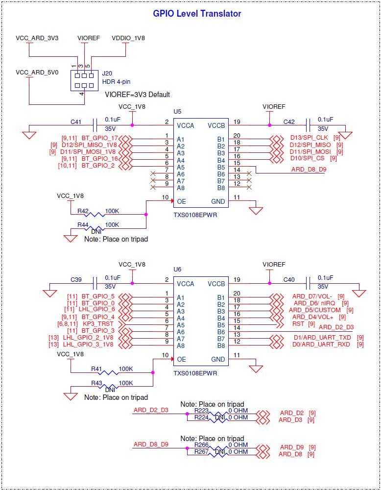
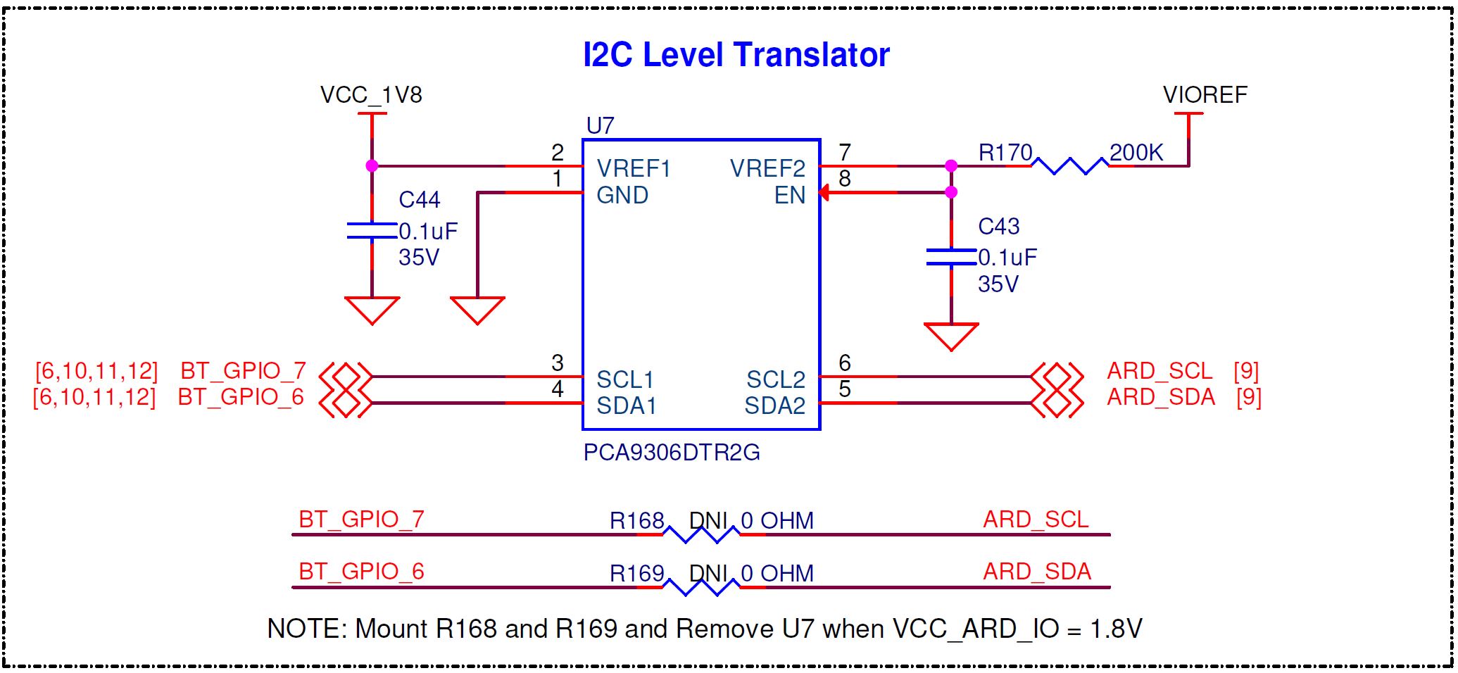
KP3 supports other serial bridges like USB-I2C and USB-SPI, as well as USB-JTAG for debugging. All serial interfaces are connected through Level translators, as the P5LP device supports 5 V and the CYW55913 device supports 1.8 V.
Baseboard power
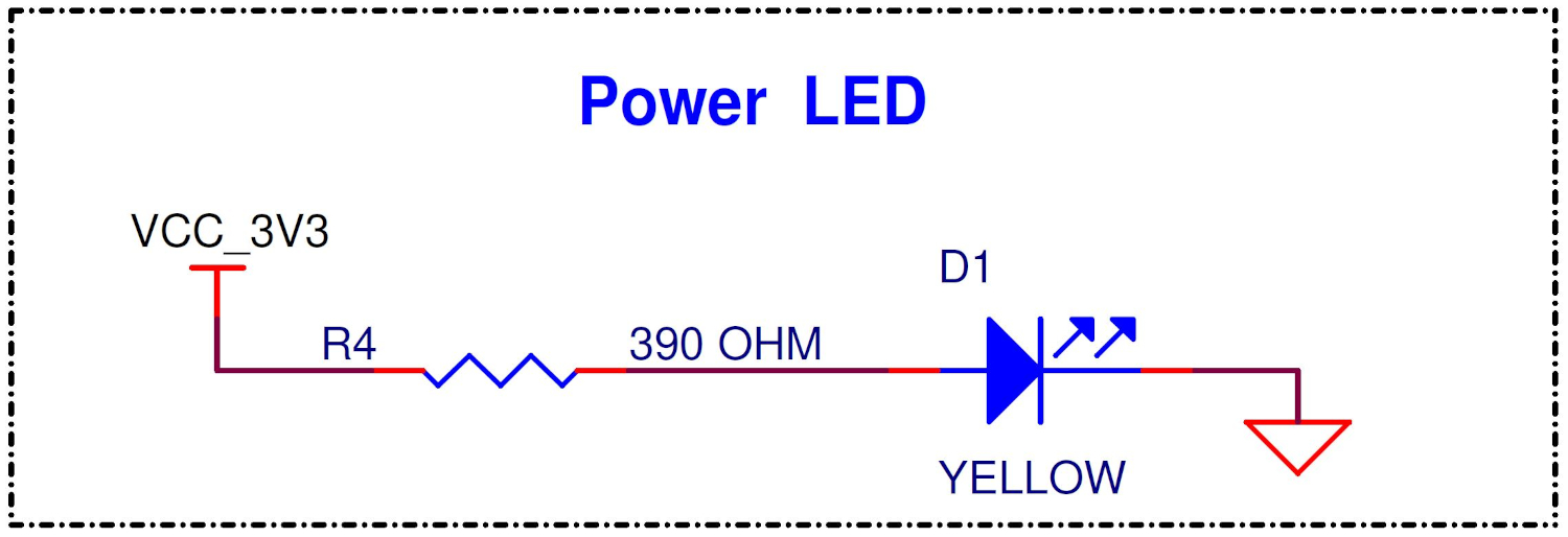
The major power supply source to this kit is the USB Type-C connector (J6) with a 20 V overvoltage protection circuit. The kit also has one optional power supply option, 5 V - 12 V DC Jack (J7). These input source sections have transient voltage suppression (TVS-diode) to provide ESD protection for the power source at the connector. The amber power LED is connected to the VCC_3V3 rail through a current-limiting resistor to indicate the board power is ON.
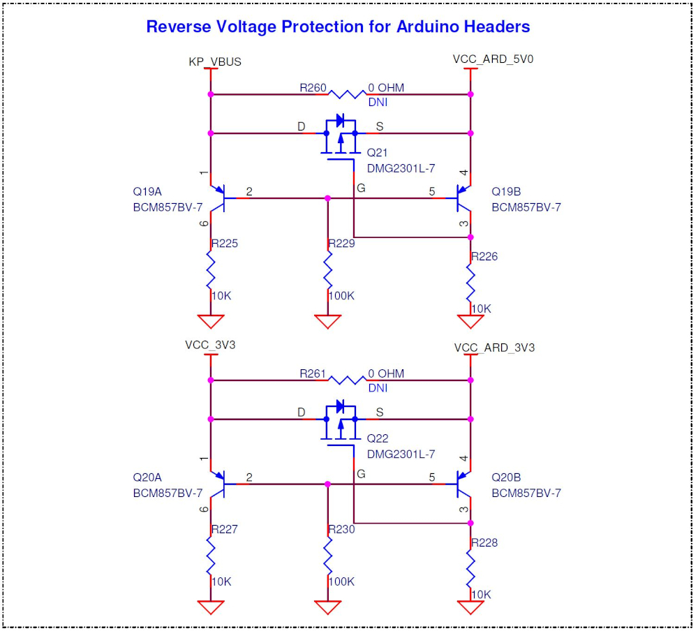
The PSOC™ 5LP (KitProg3) is powered from the KP_VBUS rail with a 0 Ω resistor/jumper in series so that PSOC™ 5LP can be disconnected from the supply rail or used as a current measurement jumper. On the other hand, KP_VBUS also goes to the Arduino header (J1) as VCC_ARD_5V0 through a reverse voltage protection circuit.
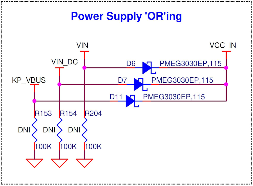
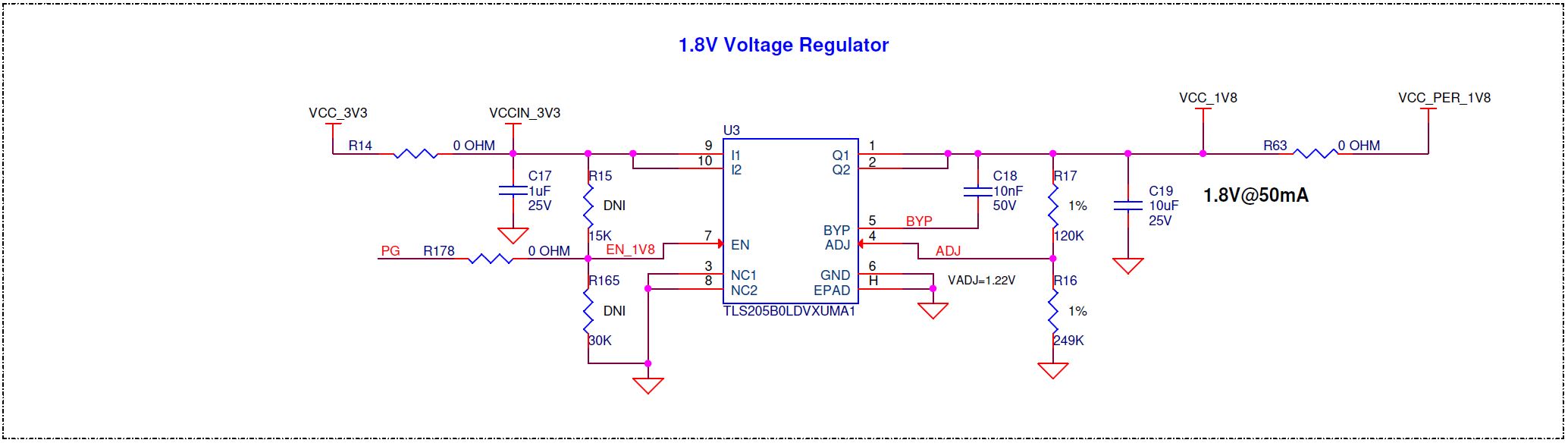
The kit has a buck regulator that generates 3.3 V from the input sources, which are combined through ORing diodes. Generated 3.3 V will be used for VBAT supply to the CYW55913 device through a current measurement jumper (J14). This 3.3 V supply is also fed to one LDO to generate 1.8 V for other peripherals on the baseboard.
5 V and 3.3 V are going to the Arduino headers via reverse voltage protection circuits, and VIOREF voltage going to the Arduino header (J1) can be selected with the jumper configuration on the J20 header.
Figure 17 shows the power architecture of the CYW955913EVK-01.
The schematics of the power supply sections of the kit are provided below.
Device recovery and reset
CYW955913EVK-01 has one recovery button and a reset button. The recovery button (SW1) connects to the BT_UART_CTS_N pin on the CYW55913 device, and while pressing the button, this pin is connected to ground and push the device into recovery mode.
SW2 on the kit is the reset button, which is connected to the BT_REG_ON pin of the CYW55913 device, and once button is pressed, it connects this pin to ground, disables the BT subsystem power supply, and makes the system reset. The BT_REG_ON pin of the device is also connected to the J17 header, and by placing jumper on the same, the BT subsystem can be permanently disabled.
Also, J16 connected to the WL_REG_ON pin of the CYW55913, should be mounted with the jumper to connect the pin always to ground.
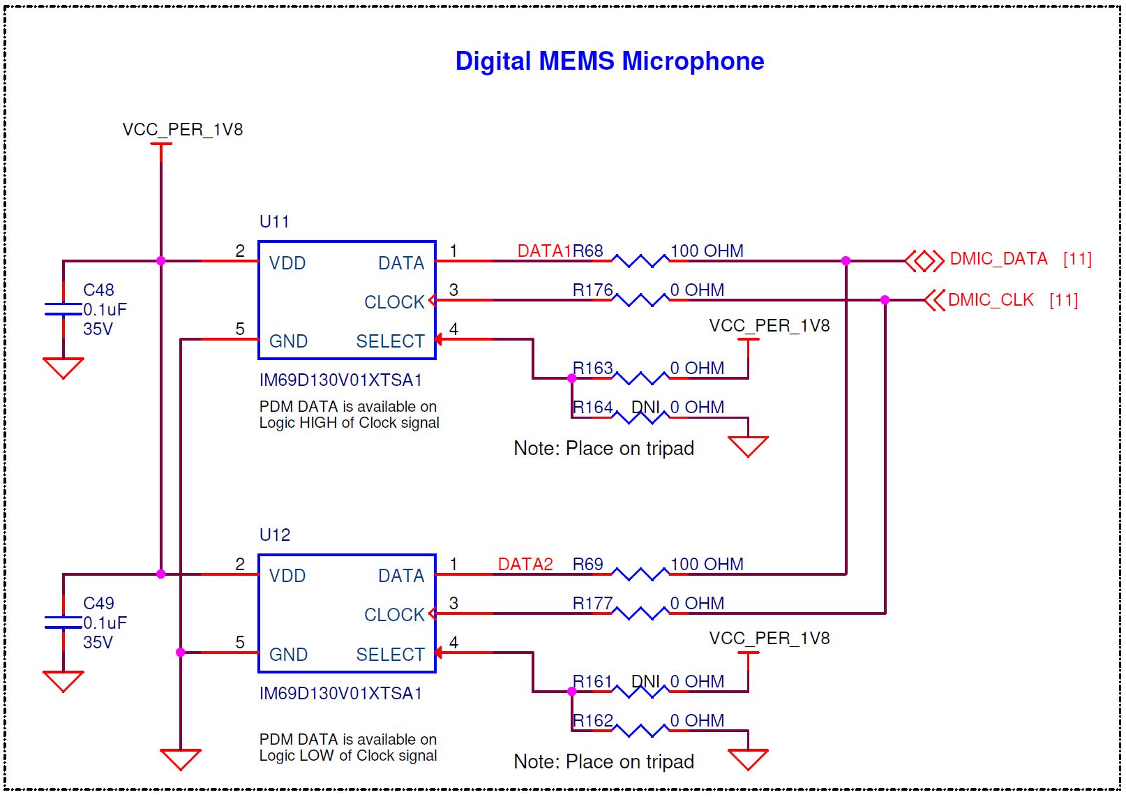
Digital (PDM) microphones
This kit has two digital mics that are connected to the CYW55913 device through the PDM interface and can be used for audio record functionalities in stereo mode. The select pin on each microphone is biased such that data is either on a HIGH or LOW of the clock signal. This digital mic is powered from the VCC_PER_1V8 power rail of the kit.
Analog microphone
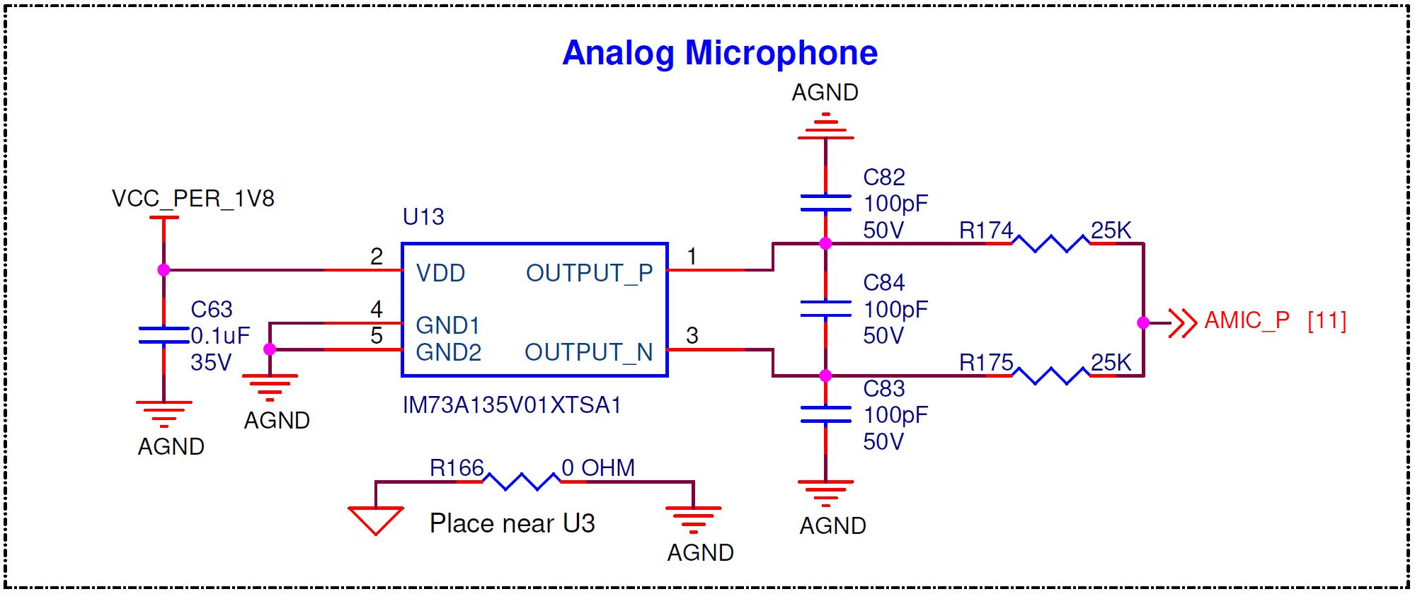
One analog microphone is also included in this kit to demonstrate the analog audio capability of the CYW55913 device. Differential output AMIC is interfaced with the CYW55913 device through the dedicated analog microphone input pin and AGND pin. This AMIC is powered by the VCC_PER_1V8 rail on the kit.
Ambient light sensor
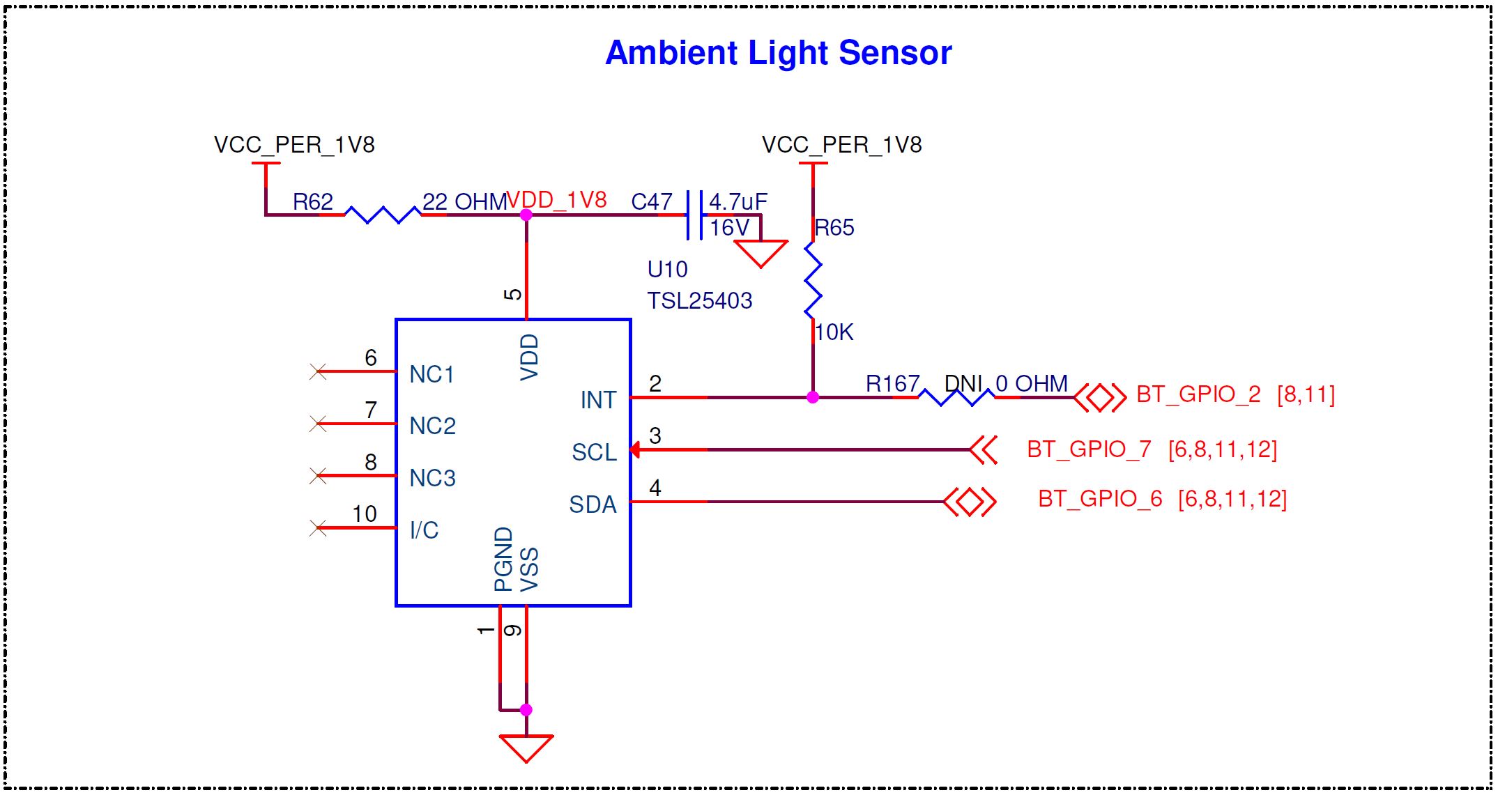
Kit is having a digital ambient light sensor on the baseboard, which is connected to the CYW55913 device via an I2C interface. The ambient light sensor is powered by the VCC_PER_1V8 power rail on the baseboard, sense the ambient light intensity, and provides data to the CYW55913 device via an I2C interface.
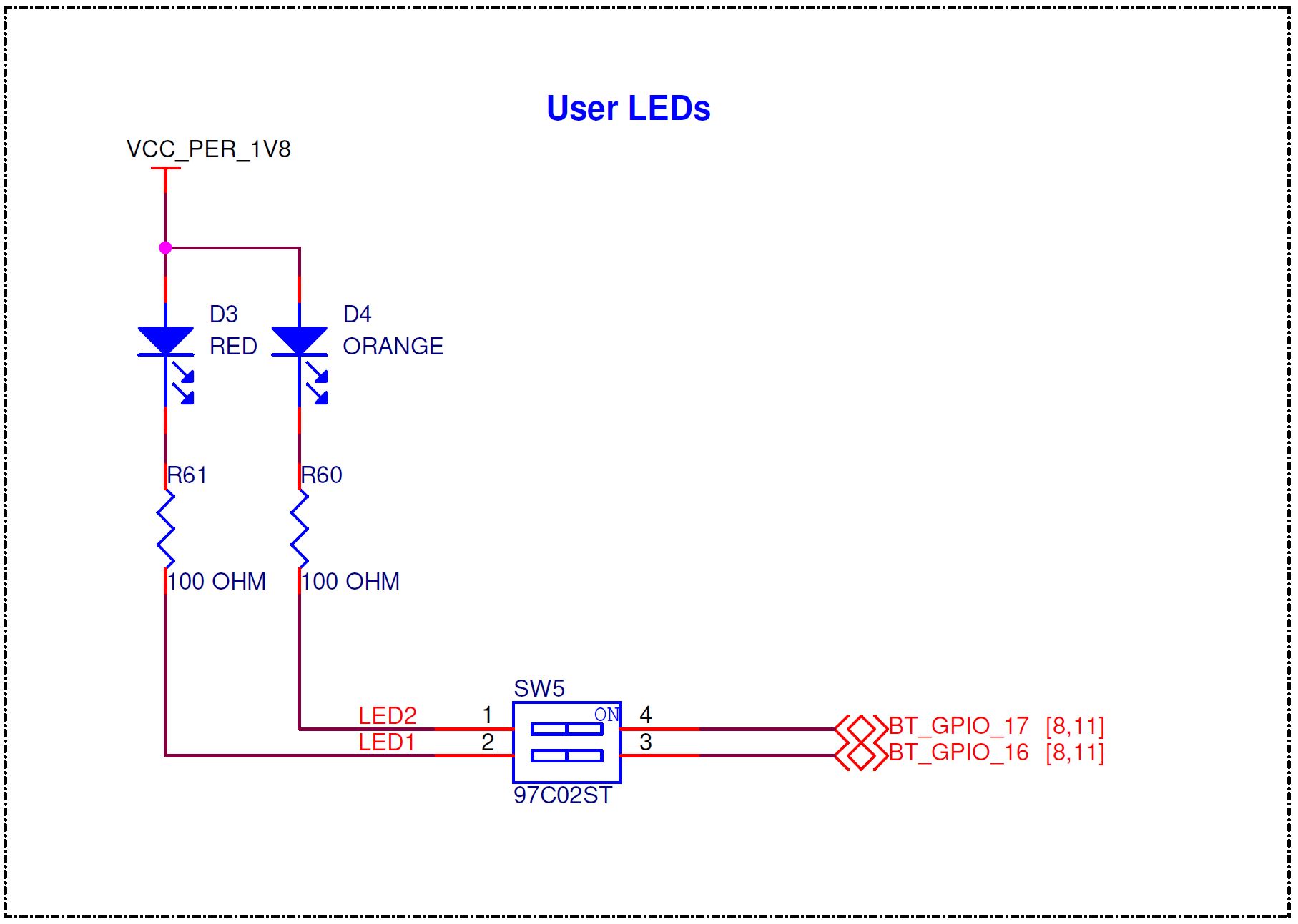
User LEDs
There are two user LEDs on the baseboard that are connected to the GPIOs of the CYW55913 device. User LED1 is connected to the BT_GPIO_16, and user LED2 is connected to the BT_GPIO_17, and these connections to the LEDs can be isolated using the SW5 switch when the GPIOs are accessed on the Arduino connectors.
LEDs are connected to the device GPIOs, so the GPIOs need to be configured as low for glowing the LEDs.
User button
One user-controlled button is available on the kit to provide user-specified inputs. This user button is connected to BT_GPIO_4 of the CYW55913 device as an active low input.
Potentiometer
One Potentiometer is present on the kit and is connected to the ADC-capable pin (LHL_GPIO_8) of the CYW55913 device that enables the kit to demonstrate the analog capability of the device.
If this GPIO is used for other functionalities on the Arduino header, the potentiometer can be disconnected from the GPIO by removing the jumper from the J10 header.
Arduino compatible headers and extended headers
The baseboard supports generic Arduino-compatible Uno shields and selected Infineon custom-defined Arduino-compatible shields. All CYW55913 GPIO pins are moved out to Arduino-compatible headers. Some pins with fixed functions are also multiplexed through 0 Ω and connected to headers. The I/O headers J1-J4 whose position and pin map comply with the Arduino-compatible UNO R3 kit to support Arduino-compatible shields.
The system power signals are moved to the pins of J1. The power supply pins for Arduino-compatible VCC_ARD_3V3 and VCC_ARD_5V0 connect to VCC_3V3 and KP_VBUS through reverse voltage protection circuits. All GPIOs of the CYW55913 device are at 1.8 V, and level translators are used to level shift them to 3.3 V, 5 V to support those voltage levels, and VIOREF voltage can be selected with the jumper position in the J20 header.
Extended headers are also available on the kit and mapped to the TDM interfaces from the CYW55913 device to support the BT audio functionality.
The SW6 slide switch is used to switch the functionalities of the multiplexed GPIOs LHL_GPIO_8 and LHL_GPIO_9.
CYW55913 device have three Serial Communication Blocks (SCBs) supports three serial communication protocols: SPI, UART, and I2C. Only one of the protocols is supported by an SCB at any given time.
In CYW955913EVK-01, SPI interface to the Arduino header J3 and the Peripheral UART available on the USB connector(J6) uses the same SCB block (SCB1). So only one of them can be accessed at any given time.
M.2 connector for CYW55913 carrier module
The M.2 E-Key standard connector (J13) is used to interface the CYW55913 M.2 carrier module to the baseboard. This connector brings out all major interfaces like HCI UART, SDIO, TDM, and GPIOs from the device.
One external LPO option is provided on the baseboard, which is connected to the pin-50 of M.2 connector to provide 32.768 kHz clock to the M.2 carrier module.
JTAG connector
Connector J9 on the baseboard maps the WL GPIOs from the CYW55913 device, which functions as the JTAG/COEX pins from the device. By default, this connector path is not mounted. See the Kit reworks chapter for the rework required to enable this path.
UART connector
To enable UART programming from an external source, the baseboard has one 6-pin header (J22), which is not mount by default. It maps the HCI UART pins from the CYW55913 device with level translated to 3.3 V.
For details of the rework required to enable this path, see the Kit reworks chapter.

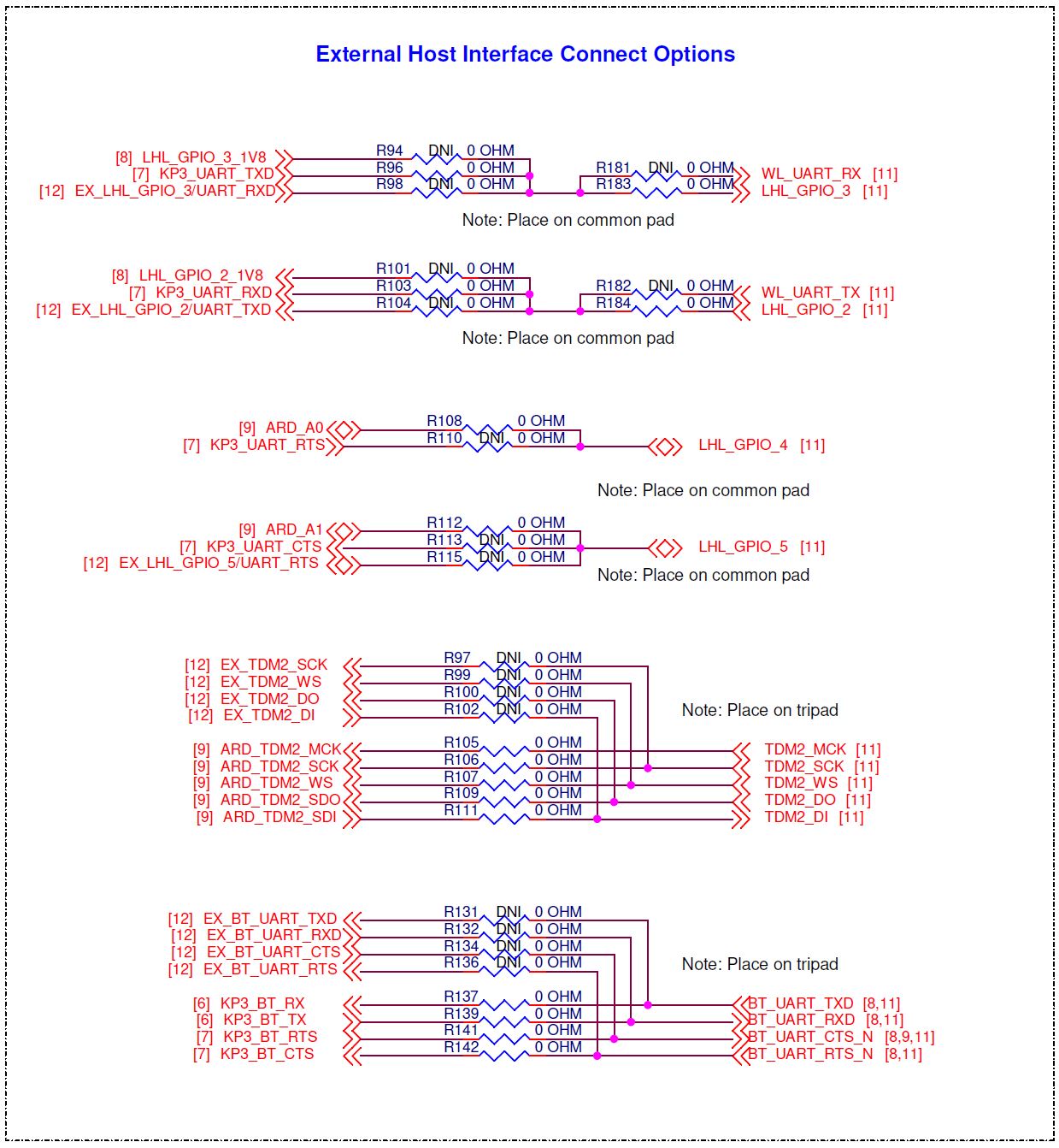
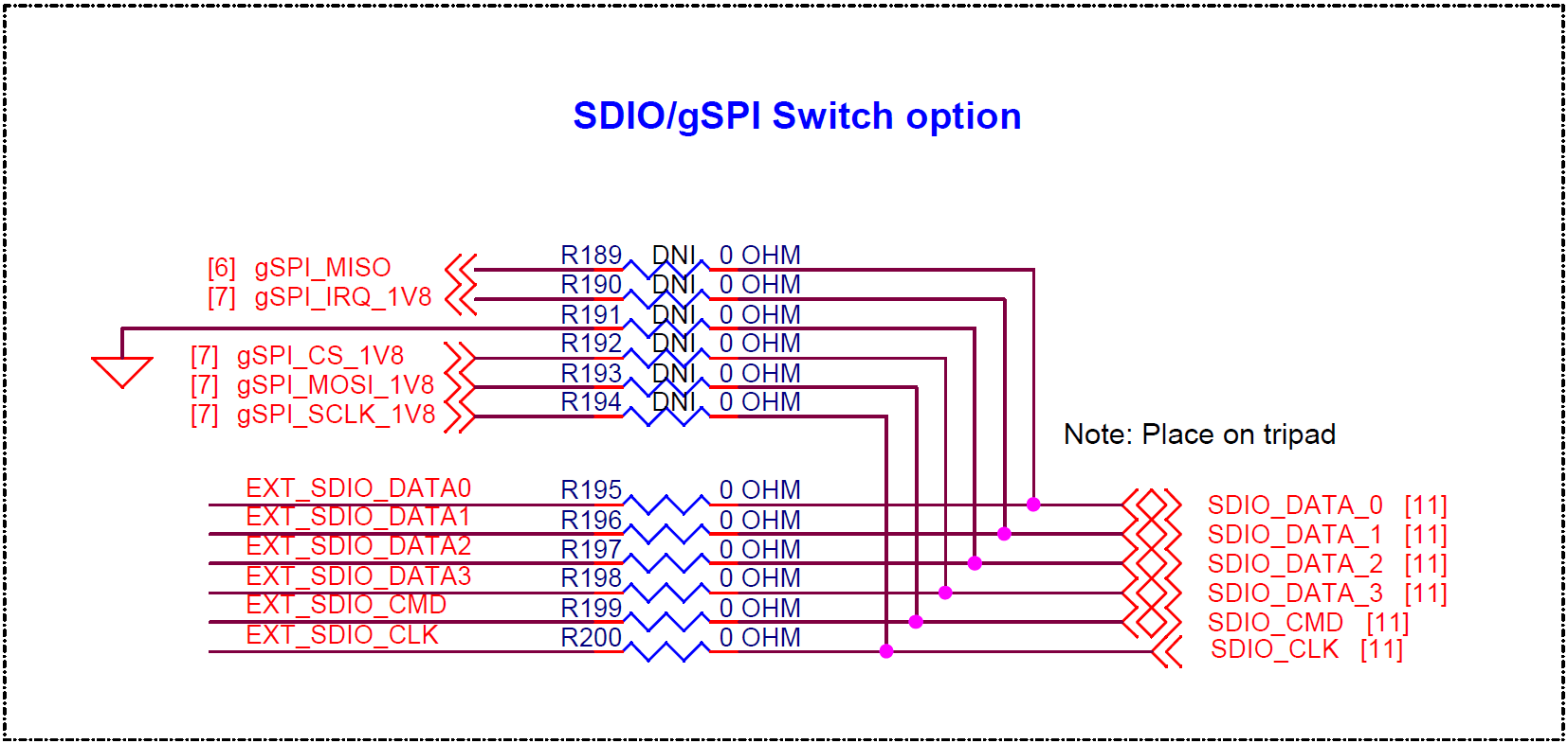
CYW55913 device I/O mapping
Table 17 gives the detailed I/O mapping of CYW55913 device and how it is connected to the peripherals and connectors on the baseboard. Baseboard connection 1 in the table defines the default configuration, and for other connection to enable, reworks may be required. See the Kit reworks chapter for more details.
| M.2 carrier module pin | M.2 carrier module pin name | CYW55913 pin | Baseboard connection 1 (Default) | Baseboard connection 2 | Baseboard connection 3 |
|---|---|---|---|---|---|
| 1 | GND | GND | GND | – | – |
| 2 | VBAT_M2 | ASR_VDDBAT WLLDO_VDDBAT BTLDO_VDDBAT | VCC_3V3 | – | – |
| 3 | BT_GPIO_2 | BT_GPIO_2 | ARD_D9 | ARD_D8 | ALS_INT |
| 4 | VBAT_M2 | ASR_VDDBAT WLLDO_VDDBAT BTLDO_VDDBAT | VCC_3V3 | – | – |
| 5 | BT_GPIO_5 | BT_GPIO_5 | ARD_D7/VOL | - | – |
| 6 | BT_GPIO_16 | BT_GPIO_16 | USER_LED1 | D10/SPI_CS | – |
| 7 | GND | GND | GND | – | – |
| 8 | TDM2_SCK | TDM2_SCK | ARD_TDM2_SCK | EX_TDM2_SCK | – |
| 9 | SDIO_CLK | SDIO_CLK | gSPI_SCLK | EXT_SDIO_CLK | – |
| 10 | TDM2_WS | TDM2_WS | ARD_TDM2_WS | EX_TDM2_WS | – |
| 11 | SDIO_CMD | SDIO_CMD | gSPI_MOSI | EXT_SDIO_CMD | – |
| 12 | TDM2_DO | TDM2_DO | ARD_TDM2_DO | EX_TDM2_DO | – |
| 13 | SDIO_DATA_0 | SDIO_DATA_0 | gSPI_MISO | EXT_SDIO_DATA0 | – |
| 14 | TDM2_DI | TDM2_DI | ARD_TDM2_DI | EX_TDM2_DI | – |
| 15 | SDIO_DATA_1 | SDIO_DATA_1 | gSPI_IRQ | EXT_SDIO_DATA1 | – |
| 16 | BT_GPIO_17 | BT_GPIO_17 | USER_LED2 | D13/SPI_CLK | – |
| 17 | SDIO_DATA_2 | SDIO_DATA_2 | GND | EXT_SDIO_DATA2 | – |
| 18 | GND | GND | GND | – | – |
| 19 | SDIO_DATA_3 | SDIO_DATA_3 | gSPI_CS | EXT_SDIO_DATA3 | – |
| 20 | BT_HOST_WAKE_M2 | BT_HOST_WAKE | J21.17 | – | – |
| 21 | GPIO0_WL_HOST_WAKE_M2 | GPIO0_WL_HOST_WAKE | J21.18 | – | – |
| 22 | BT_UART_TXD | BT_UART_TXD | KP3_BT_RX | EX_BT_UART_TXD | J22.5 |
| 23 | TDM1_WS | TDM1_WS | J5.8 | – | – |
| 32 | BT_UART_RXD | BT_UART_RXD | KP3_BT_TX | EX_BT_UART_RXD | J22.4 |
| 33 | GND | GND | GND | – | – |
| 34 | BT_UART_RTS_N | BT_UART_RTS_N | KP3_BT_CTS | EX_BT_UART_RTS | J22.2 |
| 35 | TDM1_MCK | TDM1_MCK | J5.2 | – | – |
| 36 | BT_UART_CTS_N | BT_UART_CTS_N | SW1 | KP3_BT_RTS | EX_BT_UART_CTS, J22.6 |
| 37 | TDM1_SCK | TDM1_SCK | J5.5 | – | – |
| 38 | GPIO5_WL_JTAG_TDO | GPIO5_WL_JTAG_TDO | KP3_TDO | J9.6 | – |
| 39 | GND | GND | GND | – | – |
| 40 | GPIO4_WL_JTAG_TDI | GPIO4_WL_JTAG_TDI | KP3_TDI | J9.8 | – |
| 41 | TDM1_DI | TDM1_DI | J5.6 | - | – |
| 42 | BT_DEV_WAKE_M2 | BT_DEV_WAKE_M2 | J5.4 | J21.10 | - |
| 43 | TDM1_DO | TDM1_DO | J5.7 | - | – |
| 44 | GPIO6_WL_JTAG_TRST | GPIO6_WL_JTAG_TRST | KP3_TRST | J9.10 | – |
| 45 | GND | GND | GND | – | – |
| 46 | GPIO2_WL_JTAG_TCK | GPIO2_WL_JTAG_TCK | KP3_TCLK | J9.4 | – |
| 47 | AMIC_P | MIC_P | AMIC_P | – | – |
| 48 | GPIO3_WL_JTAG_TMS | GPIO3_WL_JTAG_TMS | KP3_TMS | J9.2 | – |
| 49 | BT_GPIO_0 | BT_GPIO_0 | ARD_D6/nIRQ | – | – |
| 50 | eLPO_M2 | LPO_IN_OUT | eLPO_M2 | – | – |
| 51 | GND | GND | GND | – | – |
| 52 | TDM2_MCK | TDM2_MCK | ARD_TDM2_MCK | – | – |
| 53 | DMIC_DATA | DMIC_DQ | DMIC_DATA | – | – |
| 54 | BT_REG_ON_M2 | BT_REG_ON | SW2 | J17.1 | J21.8 |
| 55 | DMIC_CLK | DMIC_CK | DMIC_CLK | – | – |
| 56 | WL_REG_ON_M2 | NC | J16.1 | J21.7 | – |
| 57 | GND | GND | GND | – | – |
| 58 | BT_GPIO_6 | BT_GPIO_6 | KP3_SDA | ARD_SDA | J21.6 |
| 59 | LHL_GPIO_9 | LHL_GPIO_9 | D12/SPI_MISO | ARD_A3 | – |
| 60 | BT_GPIO_7 | BT_GPIO_7 | KP3_SCL | ARD_SCL | J21.5 |
| 61 | LHL_GPIO_8 | LHL_GPIO_8 | Potentiometer | D11/SPI_MOSI | ARD_A2 |
| 62 | LHL_GPIO_5 | LHL_GPIO_5 | ARD_A1 | KP3_UART_CTS | EX_LHL_GPIO_5/UART_RTS |
| 63 | GND | GND | GND | – | – |
| 64 | LHL_GPIO_4 | LHL_GPIO_4 | ARD_A0 | KP3_UART_RTS | – |
| 65 | NC | NA | - | - | - |
| 66 | WL_DEV_WAKE_M2 | WL_DEV_WAKE | J5.3 | J21.3 | – |
| 67 | LHL_GPIO_6 | LHL_GPIO_6 | ARD_D5/CUSTOM | – | – |
| 68 | LHL_GPIO_2 | LHL_GPIO_2 | KP3_UART_RXD | D1/ARD_UART_TXD | EX_LHL_GPIO_2/UART_TXD |
| 69 | GND | GND | GND | – | – |
| 70 | LHL_GPIO_3 | LHL_GPIO_3 | KP3_UART_TXD | D1/ARD_UART_RXD | EX_LHL_GPIO_3/UART_RXD |
| 71 | BT_GPIO_3 | BT_GPIO_3 | ARD_D2 | ARD_D3 | – |
| 72 | VBAT_M2 | ASR_VDDBAT WLLDO_VDDBAT BTLDO_VDDBAT | VCC_3V3 | – | – |
| 73 | BT_GPIO_4 | BT_GPIO_4 | USER_BUTTON | ARD_D4/VOL+ | – |
| 74 | VBAT_M2 | ASR_VDDBAT WLLDO_VDDBAT BTLDO_VDDBAT | VCC_3V3 | – | – |
| 75 | GND | GND | GND | – | – |
Kit reworks
This section provides details about the reworks required to enable the sections in the kit hardware that are not available by default.
JTAG connector mounting
To enable the JTAG/COEX access from the kit, you need to mount the J9 connector and resistors R211, R212, R213, and R214 to connect the CYW55913 device GPIOs to J9 and need to isolate the connection to the KP3 by removing resistors R210, R216, R217, and R218.

UART connector mounting
To enable the external UART programming, you need to mount the J22 connector and level translator (U24), which is not mounted by default. The path to the connector from CYW55913 can be enabled by mounting R219, R220, R221, and R222 resistors and removing the connections R137, R139, R141, and R142 resistors.
CYW55913 device pin multiplex options
CYW55913 device major interfaces can be switched to the external host interface or Arduino header by mounting the series resistor in the path between the device and the external connector or to the Arduino header in the multiplex options.
Revision history
|
Document version |
Date of release |
Description of changes |
|---|---|---|
|
** |
2023-09-29 |
|
| *A | 2024-03-21 | |
| *B | 2024-09-12 |
|
| *C | 2026-03-25 |
|
Trademarks
The Bluetooth® word mark and logos are registered trademarks owned by Bluetooth SIG, Inc., and any use of such marks by Infineon is under license.
PSOC™, formerly known as PSoC™, is a trademark of Infineon Technologies. Any references to PSoC™ in this document or others shall be deemed to refer to PSOC™.