CYW920829M2EVK-02 Evaluation Kit user guide
About this document
Scope and purpose
The Infineon AIROC™ CYW20829 Bluetooth® Low Energy Evaluation Kit (CYW920829M2EVK-02) enables evaluation, prototyping, and development of a wide array of Internet of Things (IoT) applications using the AIROC™ CYW20829, a low-power and high-performance Bluetooth® Low Energy MCU. The system features an Arm® Cortex® - M33 core with programmable and reconfigurable analog and digital blocks.
It is a combination of an MCU with the following:
- Sigma delta switched-cap analog-to-digital converter (ADC) for audio and DC measurements
- Seven 16-bit and two 32-bit Timer/Counter Pulse-Width Modulator (TCPWM) blocks
- 98 dBm LE-1 Mbps RX sensitivity, -105 dBm LE-LR at 125 kbps, -101 dBm LE-LR at 500 Kbps, and integrated PA with 10 dBm TX output power for better link budgets
- Serial Memory Interface (SMIF) for external flash with encryption support
- Serial communication interfaces such as UART, I2C, and Quad-SPI
- Wake from Deep Sleep I2C (sensors sitting on the I2C interface should be able to wake up the MCU)
- Two pulse density modulation (PDM) channels and one I2S channel with time division multiplexed (TDM) mode
Intended audience
This document is intended for users interested in the CYW920829M2EVK-02 kit.
Important notice
“Evaluation Boards and Reference Boards” shall mean products embedded on a printed circuit board (PCB) for demonstration and/or evaluation purposes, which include, without limitation, demonstration, reference and evaluation boards, kits and design (collectively referred to as “Reference Board”).
Environmental conditions have been considered in the design of the Evaluation Boards and Reference Boards provided by Infineon Technologies. The design of the Evaluation Boards and Reference Boards has been tested by Infineon Technologies only as described in this document. The design is not qualified in terms of safety requirements, manufacturing and operation over the entire operating temperature range or lifetime.
The Evaluation Boards and Reference Boards provided by Infineon Technologies are subject to functional testing only under typical load conditions. Evaluation Boards and Reference Boards are not subject to the same procedures as regular products regarding returned material analysis (RMA), process change notification (PCN) and product discontinuation (PD).
Evaluation Boards and Reference Boards are not commercialized products, and are solely intended for evaluation and testing purposes. In particular, they shall not be used for reliability testing or production. The Evaluation Boards and Reference Boards may therefore not comply with CE or similar standards (including but not limited to the EMC Directive 2004/EC/108 and the EMC Act) and may not fulfill other requirements of the country in which they are operated by the customer. The customer shall ensure that all Evaluation Boards and Reference Boards will be handled in a way which is compliant with the relevant requirements and standards of the country in which they are operated.
The Evaluation Boards and Reference Boards as well as the information provided in this document are addressed only to qualified and skilled technical staff, for laboratory usage, and shall be used and managed according to the terms and conditions set forth in this document and in other related documentation supplied with the respective Evaluation Board or Reference Board.
It is the responsibility of the customer’s technical departments to evaluate the suitability of the Evaluation Boards and Reference Boards for the intended application, and to evaluate the completeness and correctness of the information provided in this document with respect to such application.
The customer is obliged to ensure that the use of the Evaluation Boards and Reference Boards does not cause any harm to persons or third-party property. The Evaluation Boards and Reference Boards and any information in this document is provided "as is" and Infineon Technologies disclaims any warranties, express or implied, including but not limited to warranties of non-infringement of third-party rights and implied warranties of fitness for any purpose, or for merchantability.
Infineon Technologies shall not be responsible for any damages resulting from the use of the Evaluation Boards and Reference Boards and/or from any information provided in this document. The customer is obliged to defend, indemnify and hold Infineon Technologies harmless from and against any claims or damages arising out of or resulting from any use thereof.
Infineon Technologies reserves the right to modify this document and/or any information provided herein at any time without further notice.
Safety precautions
Note: Please note the following warnings regarding the hazards associated with development systems.
Table 1. Safety precautions
| Caution: The evaluation or reference board contains parts and assemblies sensitive to electrostatic discharge (ESD). Electrostatic control precautions are required when installing, testing, servicing or repairing the assembly. Component damage may result if ESD control procedures are not followed. If you are not familiar with electrostatic control procedures, refer to the applicable ESD protection handbooks and guidelines. |

Introduction
Infineon AIROC™ CYW20829 Bluetooth® Low Energy Evaluation Kit (CYW920829M2EVK-02) enables the evaluation, prototyping, and development of a wide array of IoT applications using the AIROC™ CYW20829, a low-power and high-performance Bluetooth® Low Energy MCU.
The AIROC™ CYW20829 Bluetooth® Low Energy MCU provides reliable Bluetooth® connectivity that is core-spec compliant to 5.4. It is a highly integrated device with an Arm® Cortex® - M33 that is dedicated to customer applications and an integrated power amplifier with 10 dBm of transmitting output power. AIROC™ CYW20829 is ideal for a wide range of applications in home and industrial automation, sensors, lighting, Bluetooth® mesh, remote controls, and any other Bluetooth® Low Energy connected IoT application.
CYW20829 Bluetooth® Low Energy EVK (CYW920829M2EVK-02) and ModusToolbox™ software and tools form a powerful but easy-to-use toolset that helps the developers to create amazing Bluetooth® enabled IoT solutions. The CYW920829M2EVK-02 offers footprint compatibility with Arduino shields. The development environment is compatible with Windows, macOS, and Linux operating systems. In addition, the kit features an onboard programmer/debugger (KitProg3). The CYW20829 Evaluation Kit supports 1.8 V, 3.3 V, and coin-cell operation.
Note: This kit supports ModusToolbox™ software 3.0 (or later).
The EVK is available through the Infineon Online Store or through our distributors.
CYW920829M2EVK-02 kit contents
The EVK includes the following:
- CYW920829M2EVK-02
- USB 2.0 Type-A to Micro-B cable
- Six jumper wires (five inches each)
- Quick start guide
Figure 1. CYW920829M2EVK-02 kit contents
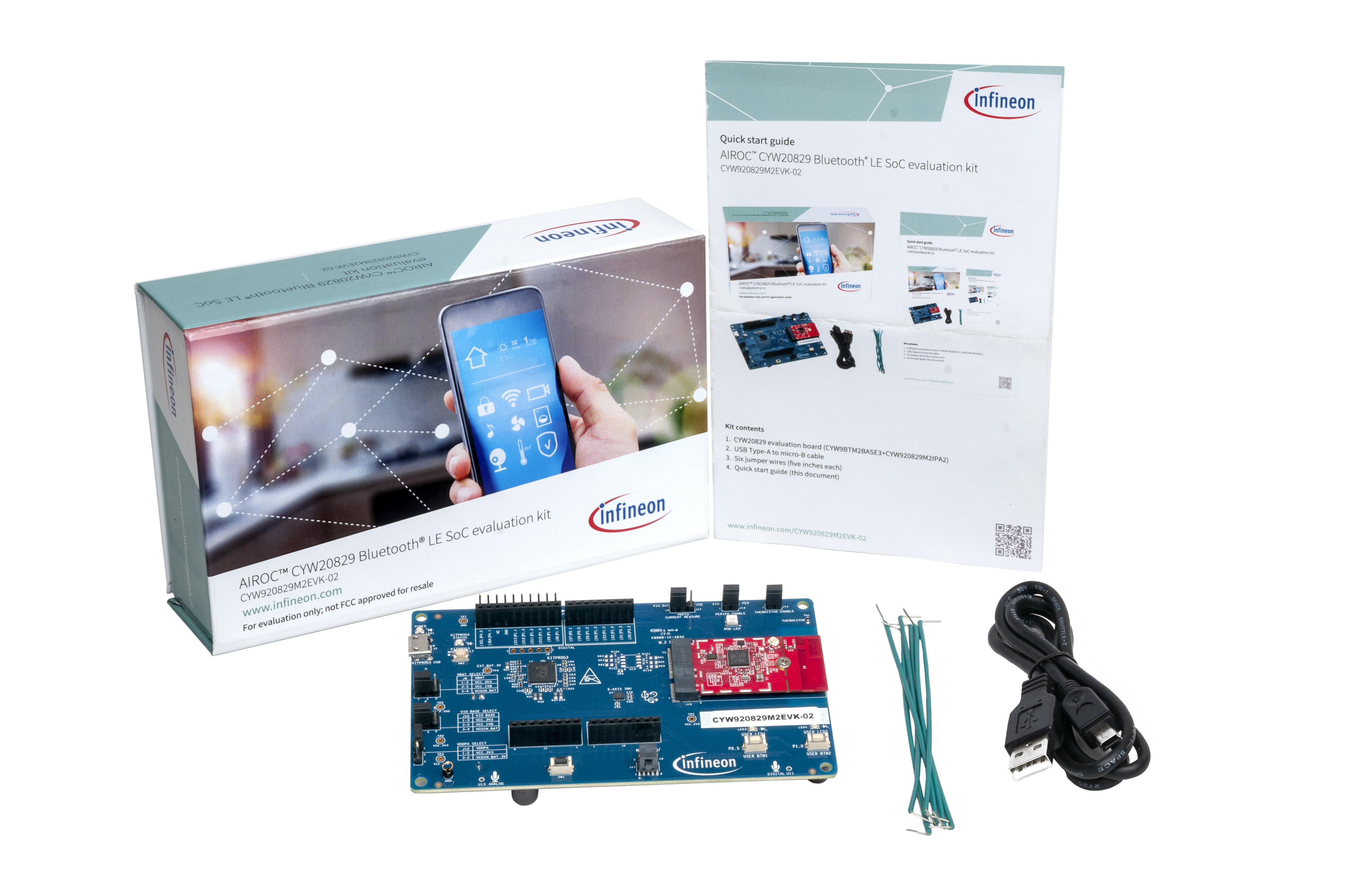
Contact the nearest Infineon sales office for assistance for any missing part in the kit contents: www.infineon.com/support.
CYW920829M2EVK-02 details
Figure 2 shows CYW920829M2EVK-02 with the following features:
- CYW20829 carrier module with onboard antenna
- Expansion headers compatible with Arduino shields
- Supports 3.3 V, coin-cell (3 V), and 1.8 V operation of the CYW920829M2EVK-02 device
- Reset button (black), User button1 (white), and User button2 (white)
- Onboard micro-USB connector (J5) for programming and debugging purposes
Follow these steps before connecting the board and verify the driver installation:
- Verify that all the jumpers are in the default configuration as shown in Table 2 to Table 7 so that the peripheral UART is selected and can display embedded application trace messages. Figure 2 shows the default jumper locations
- Connect the USB connector (J5) of the EVK to the development PC with the provided USB cable. The USB UART driver loads automatically. If the EVK is not detected as a USB device, reinstall the USB UART driver in the ModusToolbox™ installation directory
For Windows and macOS: < install>\tools_3.0\driver_media\dpinst.
For Linux: < install>\tools_3.0 \driver_media\install_driver\dpinst.
Figure 2. CYW920829M2EVK-02
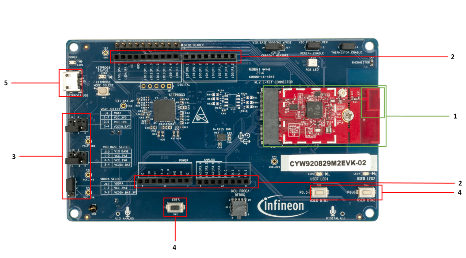
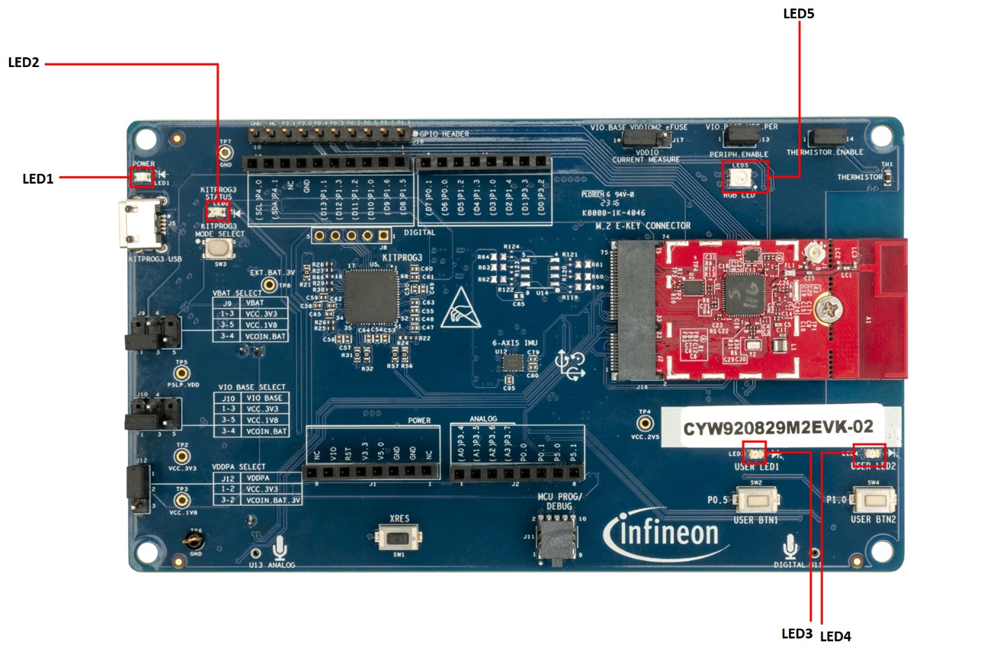
Figure 3 highlights the LEDs provided on CYW920829M2EVK-02:
- LED1 (yellow) indicates that VBAT power is ON
- LED2 (yellow) indicates KitProg3 status
- LED3 (red) and LED4 (orange) are generic user LEDs controlled by GPIOs. A label on the back of the kit provides the pin mapping
- LED5 is RGB LED which is controlled with three GPIOs
Figure 3. CYW920829M2EVK-02 LEDs
ModusToolbox
ModusToolbox™ is a free software development ecosystem that includes the Eclipse IDE for ModusToolbox™, AIROC™ BTSTACK, Bluetooth® SDK, and the PSoC™ 6 SDK to develop applications for Infineon IoT products. Eclipse IDE for ModusToolbox™ is a multi-platform, integrated development environment (IDE) used to create new applications, update application code, change middleware settings, and program or debug applications.
Using ModusToolbox™, you can enable and configure device resources and middleware libraries, write C source code, and program and debug the device. The build system infrastructure includes the new project creation wizard that can run independently of the Eclipse IDE, the make infrastructure, and other tools. This means you can choose your compiler, RTOS, and ecosystem without compromising usability or access to our industry-leading CAPSENSE™ (Human-Machine Interface), AIROC™ Wi-Fi and Bluetooth®, security, and various other features.
The Infineon’s AIROC™ BTSTACK is a software implementation of the Bluetooth® core 5.4 host protocol stack. The stack is hosted as a library on Infineon’s GitHub. The stack library includes both Bluetooth® BR/EDR and Bluetooth® Low Energy hosts and provides APIs for them. The application can choose to use Bluetooth® Low Energy or both BR/EDR + LE. The stack is available for different Arm® cores, such as CM4 and CM33, and can be used with three toolchains Arm®, GCC, and IAR.
For more details on ModusToolbox™ installation and usage, see the ModusToolbox™ user guide .
ModusToolbox code examples
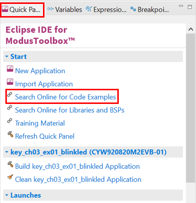
ModusToolbox™ includes many code examples. Many of these code examples are compatible with this kit. Browse the collection of starter applications during application setup through File > New > ModusToolbox™ Application or browse the collection of code examples on Infineon’s GitHub repository. See Figure 4 and Figure 5 for more details.
Figure 4. Code examples in ModusToolbox�™
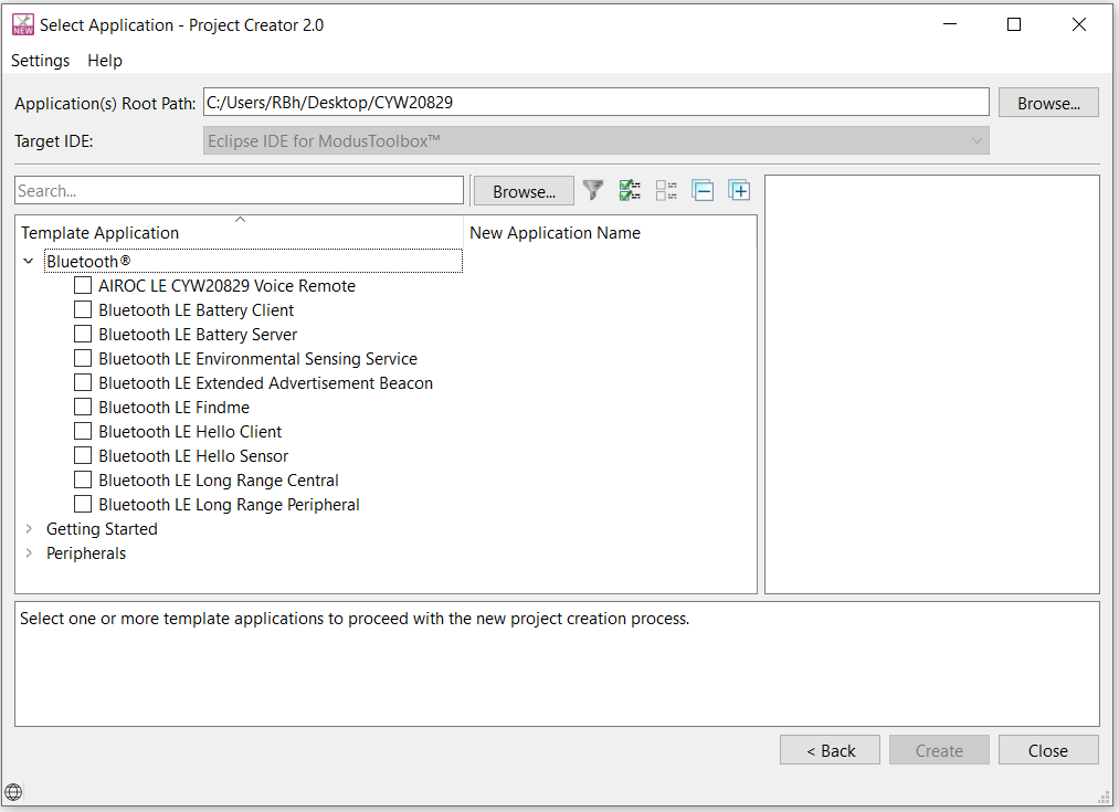
Figure 5. Searching for online code examples in ModusToolbox™
Related code examples
The kit code examples are accesses from the GitHub repository. The CYW920829M2EVK-02 is pre-programmed with the Find Me Profile (CE230297 – Bluetooth® LE Find Me Profile with CYW20829) code example out-of-the-box.
This code example is available in ModusToolbox™ as shown in Figure 4. For the most recent version of the code example, check the GitHub repository. You can find the CE230297 code example in https://github.com/Infineon/mtb-example-btstack-freertos-findme.
For more details on the functionality, design, and implementation of the code example, see the Readme present in the same folder as that of the code example. To import the most recent version of the GitHub code examples into ModusToolbox™, see the ModusToolbox™ user guide document (Help > ModusToolbox > Documentation > User guide).
ModusToolbox help
Launch ModusToolbox™ and navigate to the following items:
- Quick Start Guide: Choose Help > Eclipse IDE for ModusToolbox Documentation > Quick Start Guide. This guide gives you the basics of using ModusToolbox™
- ModusToolbox™ General Documentation: Choose Help > ModusToolbox General Documentation > ModusToolbox Documentation Index. This page provides links to various ModusToolbox™ documents
- ModusToolbox™ User Guide: Choose Help > Eclipse IDE for ModusToolbox Documentation > User Guide. This is a comprehensive guide for creating, building, and programming ModusToolbox™ applications
Getting started
This user guide helps to find the details of the CYW920829M2EVK-02 kit:
- The Kit operation chapter describes the operation of the kit and the utility of its various features
- The Hardware chapter describes the design details of the CYW920829M2EVK-02 hardware blocks
- To create a project using ModusToolbox™, see AN238254-Getting Started with AIROC™ CYW20829 Bluetooth® LE on ModusToolbox™
IoT resources and technical support
To select the right IoT device for the design, Infineon provides a wide range of product documentation at www.infineon.com/products/wireless-connectivity. Also, a professional community at community.infineon.com supplies developers with the latest software and tools to solve common evaluation and integration problems while interacting directly with both Infineon engineers and experienced peers.
Kit operation
This section provides detailed instructions to setup the Infineon CYW920829M2EVK-02 with Infineon ModusToolbox™ for Bluetooth® Low Energy (LE) applications.
This chapter introduces CYW920829M2EVK-02 and the features that are used as part of the kit’s operation. This chapter also discusses the features such as Bluetooth® connectivity, programming/debugging, and USB-UART bridge device that can be used to communicate with the CYW20829 device on this EVK.
Theory of operation
CYW920829M2EVK-02 is built around the CYW20829 device. Figure 6 shows the block diagram of the CYW20829 device. See the device datasheet for more details on device features.
Figure 6. Block diagram of CYW20829

Figure 7 illustrates the block diagram of CYW920829M2EVK-02. This board contains a CYW20829 Bluetooth® SoC and a USB-Serial interface/programmer. The kit features Arduino form-factor-compatible headers, which enable Arduino shields to be plugged in, extending the EVK’s capabilities. It also features two user switches, one reset switch, two user LEDs, a thermistor, IMU, AMIC, DMIC, and multiple power supply options.
Figure 7. Block diagram of CYW920829M2EVK-02

Figure 8 and Figure 9 show the markup of the CYW920829M2EVK-02 and the list below for a description of the numbered items.
Figure 8. CYW920829M2EVK-02 (top view)
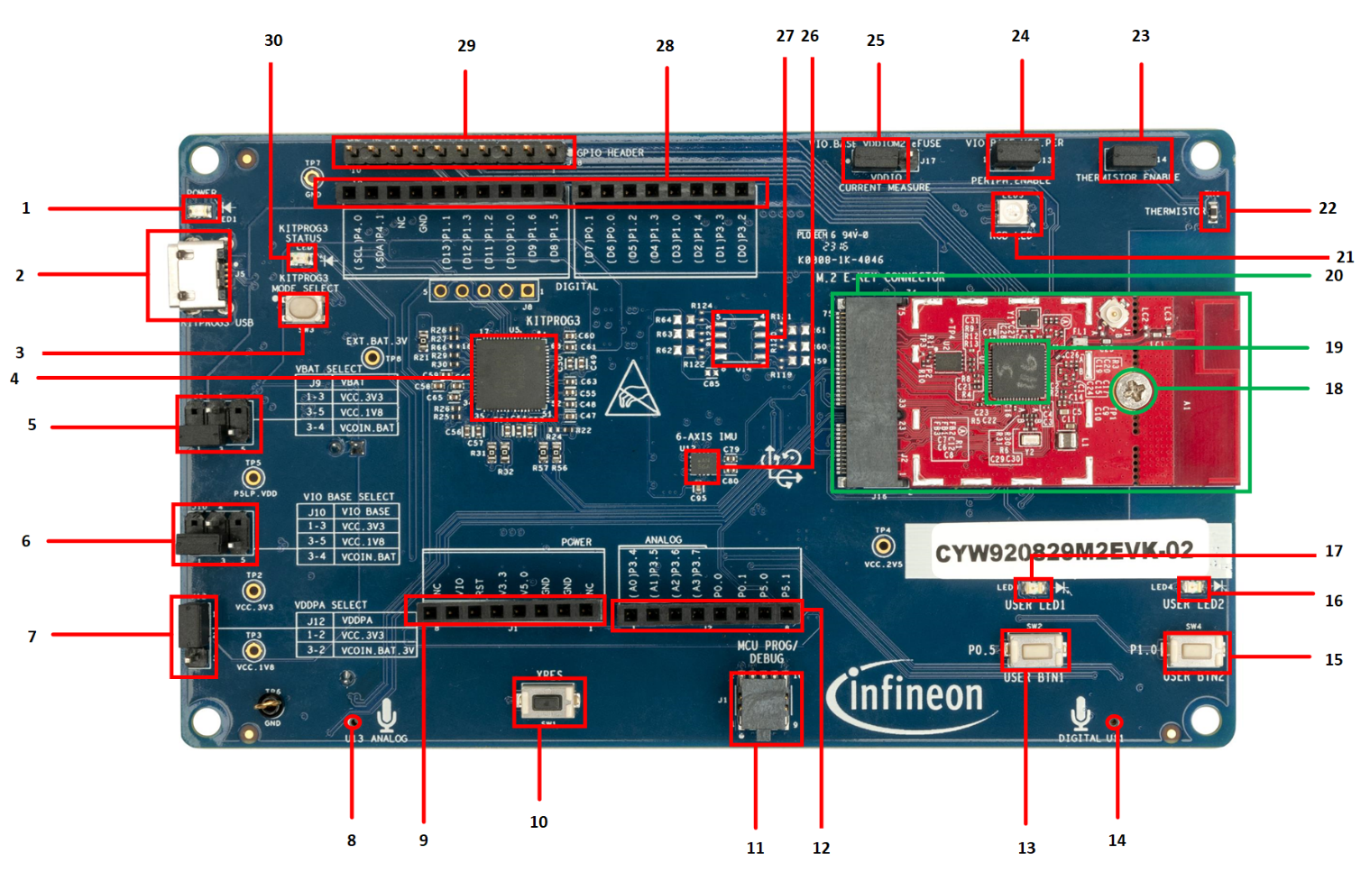
Figure 9. CYW920829M2EVK-02 (bottom view)
- Power indicator LED (LED1): This LED is used to indicate the status of power supplied to the board
- USB connector (J5): J5 is a Micro-B USB female connector for connecting the kit to the PC using the provided USB cable. It is used for programming and USB-UART communication
- KitProg3 Programming mode selection button (SW3): In this kit by default, it supports CMSIS-DAP BULK mode. The button connects the PSoC™ 5LP pin to the ground when pressed. For more details, see the KitProg3 user guide
Note: Dual UART mode is not supported because there is no hardware connection between KitProg3 and M.2 interface.
- KitProg3 (PSoC™ 5LP) programmer and debugger (CY8C5868LTI-LP039, U5): The PSoC™ 5LP (CY8C5868LTI-LP039) serving as KitProg3, is a multi-functional system, that includes a Serial Wire Debug (SWD) programmer, debugger, USB-I2C bridge, and USB-to-UART bridge. For more details, see the KitProg3 user guide
- VDDPA select jumper (J12): This jumper is used to select the VDDPA (power amplifier supply) power source. The possible selections are 3.3 V or VCOIN (3 V) which is the coin-cell power supply on the bottom side of the board
- VIO_BASE select jumper (J10): This jumper is used to select the VIO_BASE power source. Possible selections are 3.3 V, 1.8 V, or VCOIN (3 V), which is the coin-cell power supply on the bottom-side of the board
- VBAT select jumper (J9): This jumper is used to select the VPA_BT (core power supply) power source. The possible selections are 3.3 V, 1.8 V, or VCOIN (3 V) which is the coin-cell power supply on the bottom-side of the board
- Analog mic (U13): It can be used to configure the kit as a voice remote
- Arduino-compatible header (J1): The Arduino-compatible I/O header brings out power and reference voltage pins from the base board to interface with Arduino shields
- Reset button (SW1, XRES): This button can be used to reset the device
- Debug header (J13): J13 is a 10-pin interface header that can be used to connect an external programmer/debugger via SWD
Note: Use J13 only to connect a programmer/debugger. A voltage mismatch occurs if something else is connected to J13 to communicate with KitProg3.
- Arduino-compatible header (J2): The Arduino-compatible I/O header brings out pins from CYW20829 to interface with Arduino shields
- User button1 (SW2): This button can be used to provide input to the CYW20829 device. Note that the button connects the CYW20829 pin to the ground when pressed; therefore, the CYW20829 pin must be configured as a digital input with a resistive pull-up for detecting the button press
- Digital mic (U11): The digital microphone ASIC contains an extremely low-noise preamplifier and a high-performance sigma-delta ADC. It can be used to configure the kit as a voice remote
- User button2 (SW4): This button can be used to provide input to the CYW20829 device. Note that the button connects the CYW20829 pin to the ground when pressed; therefore, the CYW20829 pin must be configured as a digital input with a resistive pull-up for detecting the button press
- User LED2 (LED4): These onboard LEDs can be controlled by the CYW20829 device. The LEDs are ACTIVE LOW; therefore, these pins must be driven low to turn ON the LEDs
- User LED1 (LED3): These onboard LEDs can be controlled by the CYW20829 device. The LEDs are ACTIVE LOW; therefore, these pins must be driven low to turn ON the LEDs
- M.2 Stand Off (MT1): Stand to connect M.2 card
- CYW20829 (U1): The Bluetooth® Low Energy 5.4 qualified system-on-chip from the Infineon is the heart of this evaluation kit
- M.2 E key connector (J16): This is used to interface Infineon custom Bluetooth® Low Energy M.2 boards to this kit
- RGB LED (LED5): These onboard LEDs can be controlled by the CYW20829 device. The LEDs are ACTIVE LOW; therefore, these pins must be driven to the ground to turn ON the LEDs
- Thermistor (TH1): The onboard thermistor is an NTC analog thermistor that can be used to measure temperature
- Thermistor enable jumper (J14): This jumper can be used to connect or disconnect the onboard thermistor from the CYW20829 device
- Peripheral enable (J13): The jumper allows the user to connect and disconnect the VDDIO supply to onboard peripheral devices such as the IMU, thermistor, analog mic, and real-time clock by disabling VDDP
- VDDIO current measurement jumper (J17): This jumper is used to power the carrier module. Remove this jumper and connect an ammeter to the two pins to measure the current the carrier module uses
- 6-axis IMU(U12): This is an I2C-based 6-axis IMU sensor
- 1-MB serial flash (U14): This is the 1-MB QSPI flash used for application purposes (no load by default)
- Arduino-compatible header (J4 and J3): The Arduino-compatible I/O header brings out pins from CYW20829 to interface with Arduino shields
- Digital I/O headers (J18): Extended GPIO headers for extending the additional GPIOs from the CYW20829 device
- KitProg3 status indication LED (LED2): This yellow LED indicates the status of KitProg3
- Coin cell holder (BT1): This is a coin cell battery holder located on the bottom side of the development kit. If the EVK needs to use the power supplied from the coin cell, then set the VBAT, VIO_BASE, and VDDPA select headers to VCOIN
Jumpers
Table 2 to Table 7 list the jumper settings on the CYW920829M2EVK-02.
Table 2. Jumper J9 pin configurations
Jumper J9 (VBAT selection) | Default state | Connection on CYW20829 | Description |
|---|---|---|---|
1 and 3 | Shorted | VBAT | Short these pins to supply 3.3 V to VBAT of the CYW20829 device |
3 and 5 | Open | Short these pins to supply 1.8 V to VBAT of the CYW20829 device | |
3 and 4 | Open | Short these pins to supply the VBAT of the CYW20829 device from the coin cell supply (VCOIN) |
Table 3. Jumper J10 pin configurations
Jumper J10 (VIO_BASE selection) | Default state | Connection on CYW20829 | Description |
|---|---|---|---|
1 and 3 | Shorted | VDDIO | Short these pins to supply 3.3 V to VIO_BASE of the CYW20829 device, as well as all peripherals and sensors |
3 and 5 | Open | Short these pins to supply 1.8 V to VIO_BASE of the CYW20829 device, as well as all peripherals and sensors | |
3 and 4 | Open | Short these pins to supply VIO_BASE of the CYW20829 device, as well as all peripherals and sensors from the coin cell supply (VCOIN) |
Table 4. Jumper J12 pin configurations
Jumper J12 (VDDPA selection) | Default state | Connection on CYW20829 | Description |
|---|---|---|---|
1 and 2 | Shorted | VDDPA | Short these pins to supply 3.3 V to VDDPA of the CYW20829 device. Also, use this jumper to measure the current consumption of VDDPA when using a 3.3 V supply |
2 and 3 | Open | Short these pins to supply VCOIN to VDDPA of the CYW20829 device. In addition, use this jumper to measure the current consumption of VDDPA when using the coin cell supply (VCOIN) |
Table 5. Jumper J14 pin configuration
Jumper J14 (Thermistor connect/disconnect) | Default state | Connection on CYW20829 | Description |
|---|---|---|---|
1 and 2 | Shorted | P3.4 | Short this jumper to connect the onboard thermistor to CYW20829 |
Table 6. Jumper J17 pin configuration
Jumper J17 (VDDIO current measurement) | Default state | Connection on CYW20829 | Description |
|---|---|---|---|
1 and 2 | Shorted | VDDIO_1, VDDIO_2, VDDIO_A, VDDA | Short this jumper to supply power to the I/O domain (VDDIO) of CYW20829. In addition, use this jumper to measure the current consumption of the I/O domain |
Table 7. Jumper J13 pin configuration
Jumper J13 (Peripheral enable) | Default state | Connection on CYW20829 | Description |
|---|---|---|---|
1 and 2 | Shorted | NA | Allows power to onboard peripherals such as IMU, Flash, DMIC, AMIC, Thermistor, and LEDs |
Buttons and switches
Table 8. Button functionality
Buttons | Pressed state | Connection on CYW20829 | Description |
|---|---|---|---|
SW1 | GND | BT_RST_N | ACTIVE LOW Reset button (black) |
SW2 | GND | P0.5 | User application button (white) |
SW3 | GND | NA | Switch allows you to change the KP3 mode |
SW4 | GND | P1.0 | User application button (white) |
Arduino-compatible headers
J3, J4, J1, and J2 are Arduino-compatible headers.
Table 9. Header J3 pin configuration
Header J3 | Arduino pin | Connection on CYW20829 | Description |
|---|---|---|---|
1 | D8 | P1.5 | GPIO |
2 | D9 | P1.6 | GPIO |
3 | D10 | P1.0 | GPIO |
4 | D11 | P1.2 | GPIO |
5 | D12 | P1.3 | GPIO |
6 | D13 | P1.1 | USER_LED1 |
7 | GND | GND | Ground |
8 | NC | NC | NC |
9 | SDA | P4.1 | I2C SDA |
10 | SCL | P4.0 | I2C SCL |
Table 10. Header J4 pin configuration
Header J4 | Arduino-compatible pin | Connection on CYW20829 | Description |
|---|---|---|---|
1 | D0 | P3.2 | GPIO |
2 | D1 | P3.3 | GPIO |
3 | D2 | P1.4 | GPIO |
4 | D3 | P1.0 | GPIO |
5 | D4 | P1.3 | GPIO |
6 | D5 | P1.2 | GPIO |
7 | D6 | P0.0 | GPIO |
8 | D7 | P0.1 | GPIO |
Table 11. Header J1 pin configuration
Header J1 | Arduino-compatible pin | Connection on CYW20829 | Description |
|---|---|---|---|
1 | NC | NC | NC |
2 | GND | GND | Ground |
3 | GND | GND | Ground |
4 | 5V | VDD5V | 5 V supply output to the Arduino Shield |
5 | 3V3 | VDD3P3 | 3.3 V supply output to the Arduino Shield |
6 | RST_N | XRES | Arduino Reset |
7 | VIO_BASE_LOAD | VDDIO | I/O reference pin used by shields to determine the I/O voltage. Connected to VDDIO on this board. Therefore, IOREF follows 1.8 V or 3.3 V, or VCOIN of VDDIO |
8 | NC | NC | NC |
Table 12. Header J2 pin configuration
Header J2 | Arduino-compatible pin | Connection on CYW20829 | Description |
|---|---|---|---|
1 | A0 | P3.4 | GPIO |
2 | A1 | P3.5 | GPIO |
3 | A2 | P3.6 | GPIO |
4 | A3 | P3.7 | GPIO |
5 | A4 | P0.0 | GPIO |
6 | A5 | P0.1 | GPIO |
7 | A6 | P5.0 | GPIO |
8 | A7 | P5.1 | GPIO |
Note: When accessing the Arduino pins, remove the jumpers that may interfere with the Arduino-compatible pins, such as thermistor jumper, USER LED, and RGB LED resistors.
Other headers
J18 is the test header which brings out certain pins of CYW20829 for testing.
Table 13. Header J18 pin description
Header J18 | Connection to header pin | Connection on CYW20829 | Description |
|---|---|---|---|
1 | USER LED1 | P1.1 | This onboard LED can be controlled by the CYW20829 device |
2 | USER LED2 | P5.2 | This onboard LED can be controlled by the CYW20829 device |
3 | USER BTN1 | P0.5 | This button can be used to provide input to the CYW20829 device |
4 | GPIO1 | P0.2 | GPIO |
5 | GPIO2 | P0.3 | GPIO |
6 | GPIO3 | P0.4 | GPIO |
7 | GPIO4 | P3.0 | GPIO |
8 | GPIO5 | P3.1 | GPIO |
9 | NC | NC | No connection |
10 | GND | GND | Ground |
J11 is a 10-pin programmer/debugger header to debug CYW920829M2EVK-02 using SWD.
Table 14. Header J11 pin description
Header J11 | Connection to header pin | Connection on CYW20829 | Description |
|---|---|---|---|
1 | VDDIO | VDDIO | VDDIO reference |
2 | D5/SWDIO | P1.2 | SWD input output |
3 | GND | GND | Ground |
4 | D4/SWDCK | P1.3 | SWD clock |
5 | GND | GND | Ground |
6 | NC | NC | No connect |
7 | GND | GND | Ground |
8 | NC | NC | No connect |
9 | GND | GND | Ground |
10 | SWD_RST | BT_RST_N | CYW20829 device reset |
Note: J11 must be used only to connect a programmer/debugger. If not, a voltage mismatch can occur.
USB serial interface chip
CY8C5868LTI-LP039 PSoC™ 5LP chip for onboard programming and USB-Serial functionality. It connects to the PC over a USB interface and to the CYW20829 device through the HCI UART and I2C pins.
Kit power supply
Power the kit with one of the two power sources: USB or coin-cell battery.
As shown in Figure 7, the USB power is connected to two buck regulators, one regulating the voltage to 1.8 V and the other to 3.3 V. A coin-cell battery can be directly connected without the need for a regulator. See Table 2, through Table 7 to understand the jumper settings for power selection.
Test points
There are two ground test points for easy connection of probes. The voltage from various power domains can be measured from their respective TPs.
Table 15. Test points available in CYW920829M2EVK-02
Label | Description |
|---|---|
TP7, TP6 | Test points for ground |
TP2 | Test point for 3.3 V |
TP3 | Test point for 1.8 V |
TP4 | Test point for 2.5 V |
TP5 | VDD for P5LP |
TP8 | Test point for 3.0 V from external coin cell battery |
Current measurement
The CYW20829 device has two power domains:
- VIO_BASE to power the always ON GPIO pins
- VBAT to power the core
The sum of the current consumed by the VIO_BASE and VBAT power domains is the device’s total current consumption.
- To measure the current consumed by the VIO_BASE domain, connect an ammeter across pin 1 and 2 of jumper J17.
- To measure the current consumed by the VBAT domain, connect an ammeter across pin 3, and one of pins 1 or 4 or 5 (depending on the power source) of jumper J9.
SWD debugging
ModusToolbox™ supports multiple Arm®-JTAG adapters for debugging Bluetooth® products such as CYW20829. Debugging is possible on CYW920829M2EVK-02 through SWD signals. SWD is a 2-wire interface that uses SWD input output (SWDIO) and serial wire clock (SWDCLK) for debugging the device. In CYW920829M2EVK-02, P1.2 act as SWDIO, and P1.3 act as SWDCLK. See Table 14 to enable the SWD pins to the debug connector (J11).
Note: The SWD and SPI (MISO and MOSI) interfaces share the same GPIOs and must use one interface at a time.
Figure 10. SWD debugging
Pin configuration
GPIOs on the CYW20829 device can be multiplexed to various peripherals. For more information on the peripherals that can be routed to the various GPIOs, see the device datasheet.
For this board, the ModusToolbox™ initializes GPIOs to the platform’s default configuration.
Hardware
This chapter describes the CYW920829M2EVK-02 hardware and its different blocks, such as reset control, Arduino-compatible headers, and module connectors.
See the CYW920829M2EVK-02 kit page for schematics for the baseboard and carrier module.
Carrier module
The baseboard design of the CYW920829M2EVK-02 board is a modular so that various carrier modules can be used with the same baseboard. In this kit, the CYW920829M2IPA2 carrier M.2 radio card module, which employs the CYW20829 device, is connected to the baseboard through M.2 interface. The carrier module interface is a generic interface used across many devices. See CYW20829 device I/O mapping for a detailed interface description. The Bluetooth® antenna is etched on the carrier module PCB. UART signals and GPIOs are brought out from module pins to interface with the baseboard.
CYW20829
The CYW920829M2EVK-02 board employs the CYW20829 device which is a 56-pin QFN package. This board uses all 26 GPIOs provided by the 56-pin QFN package.
Antenna
A PCB antenna is etched on the carrier module. This antenna is matched to 50 Ω when the CYW920829M2EVK-02 board is placed on a table. Table 16 lists the S11 measurement. See AN91445 – Antenna design and RF layout guidelines for additional information.
Table 16. Antenna S11 measurement
2402 MHz | 2441 MHz | 2480 MHz |
|---|---|---|
-13.2 dB | -14.6 dB | -12.6 dB |
Crystal
The CYW20829 carrier module has two crystals onboard. A 24-MHz crystal (XTAL) is the main crystal. This XTAL must have an accuracy of +/-20 ppm as defined by the Bluetooth® specification. A 32.768-kHz crystal provides accurate timing during low-power operation. See the CYW20829 datasheet for crystal requirements.
Baseboard
CYW9BTM2BASE3 is a baseboard on which the CYW20829 carrier module is connected. This baseboard provides various sensors to interface with CYW20829 device.
Serial communication between CYW20829 and PSoC 5LP KitProg3
The onboard CY8C5868LTI-LP039 PSoC™ 5LP device is a true programmable embedded system-on-chip responsible for two-channel USB-serial conversion on this baseboard. The USB-serial pins of the PSoC™ 5LP device are hard-wired to the HCI UART pins of the CYW20829 device.
Use mode switch SW3 to switch between various modes of operation of KitProg3. Note that this board supports only CMSIS-DAP BULK mode. This button function is reserved for future use. The status LED (LED5) indicates the current mode of KitProg3.
Figure 11. Serial communication between CYW20829 and PSoC™ 5LP KitProg3

Power
The power supply system on this board is versatile, allowing the input supply to come from the following sources:
- 5 V from KitProg3 micro USB Type-B port
- 3 V from coin-cell
These input source sections can have transient voltage suppression (TVS-diode) to provide ESD protection for the power source at the connector.
The amber power LED is connected to the VCC_3V3 rail through a current limiting resistor to indicate the board power is ON.
The PSoC™ 5LP (KitProg3) is powered from the KP_VBUS rail with a 0- Ω resistor/jumper in series so that PSoC™ 5LP can be disconnected from the supply rail easily or can be used as a current measurement jumper. On the other hand, KP_VBUS also goes to the Arduino Header (J1) as VCC_ARD_5V0 through a reverse voltage protection circuit.
The kit can have a buck regulator that generates 3V3, 2V5, and 1V8 for VBAT/VDDIO/VDDPA and eFuse voltages of CYW20829 devices.
The regulated output VCC_1V8 from LDO will go to the peripherals: IMU, Thermistor, DMIC, RGB LED, and AMIC through jumper and Arduino-compatible header as VDDIO reference through reverse voltage protection.
Table 16 shows the power architecture of the CYW920829M2EVK-02.
Figure 12. Power architecture of CYW20829M2EVK-02
Select the power supply options via jumper settings on J9, J10, and J12. See Table 2, Table 3, and Table 4 for the different jumper settings for these jumpers. Resistors R39 and R40 are pull-up resistors for the I2C lines to the IMU, that is., SCL and SDA. Short the J13 (PERIPHERAL ENABLE) for any I2C devices to be connected, because the pull-up voltages for SCL and SDA are supplied from VCC_PER. Power input for the kit is driven through a micro USB input connector. Generate the required voltages 3V3, 1V8, and 2V5 using the Infineon LDOs.
Figure 13. 5 V power supply from USB
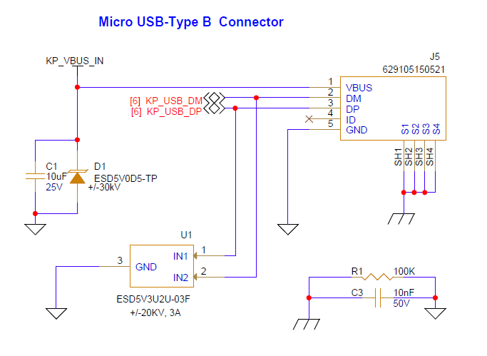
Figure 14. 3V3 regulator circuit
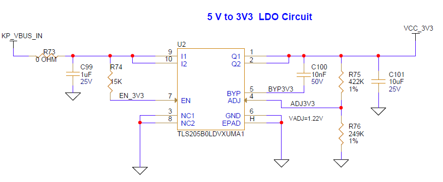
Figure 15. 1V8 regulator circuit

Figure 16. 2V5 regulator circuit
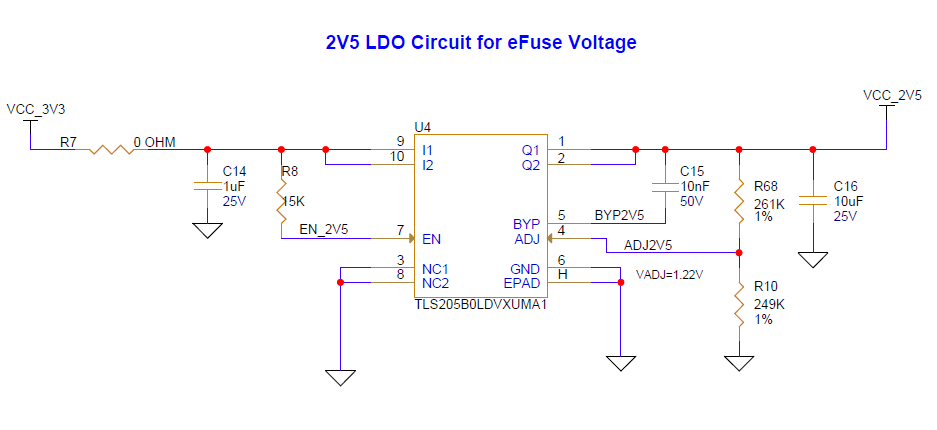
Figure 17. Jumper J10 for VDDIO selection
Figure 18. Jumper J9 for VBAT selection

Figure 19. Jumper J12 for VDDPA selection
Device reset
The reset circuit on the board consists of a reset button (SW1) connected to the ground with an optional pull-up resistor and decoupling capacitor. Release the BT_RST_N on the CYW20829 with the delay of 50 ms or more after the VDDIO supply voltage has stabilized. The voltage-detector IC is used to provide this delay.
Figure 20. Reset button circuit in baseboard
Figure 21. Voltage detector circuit in the carrier module
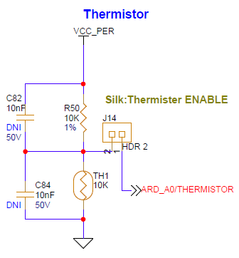
Thermistor
The thermistor circuit is a simple voltage divider circuit consisting of an NTC thermistor that is 10 kΩ at 25°C and a fixed 10 kΩ resistor. The divided voltage is fed into A0, and the voltage level determines the ambient temperature. The part number of the thermistor used on this kit is NCP18XH103F03RB.
Figure 22. Thermistor circuit
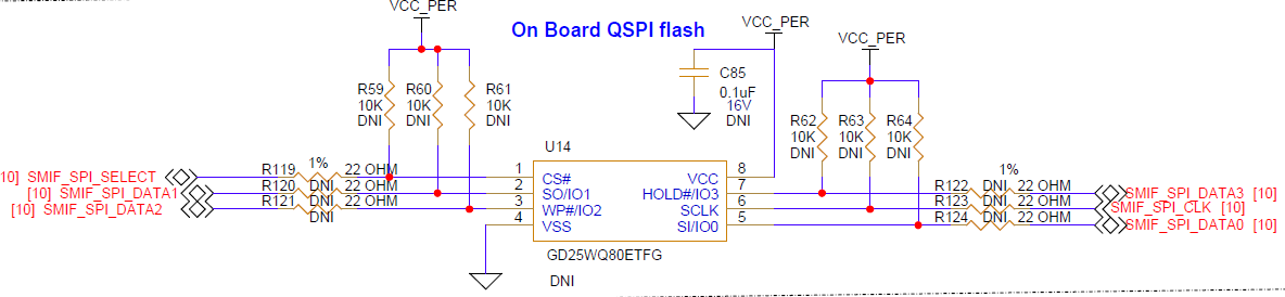
External serial flash
CYW920829M2EVK-02 has a GigaDevice 8-Mbit serial flash (GD25WQ80ETFG) on the baseboard, which can be useful when the user application requires more memory. The Bluetooth® SDK is compatible with most JEDEC CFI-compliant SPI flash ICs. The SPI driver should configure the respective pins in the user application in order to use the onboard serial flash (no load by default).
Figure 23. External serial flash
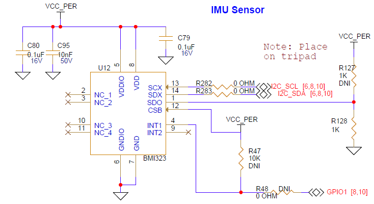
Inertial measurement unit (IMU)
An onboard IMU sensor will be available to sense the position of the kit, used to measure the acceleration and angular velocity, when combined with sensor fusion software. This can be used to determine the motion, orientation, and heading of the kit. The CYW20829 device communicates with this sensor over I2C. By default, the I2C address is ‘0x68’, and can be changed using the resistor options (R127 and R128). See the BMI323 datasheet for more details.
Figure 24. IMU sensor circuit
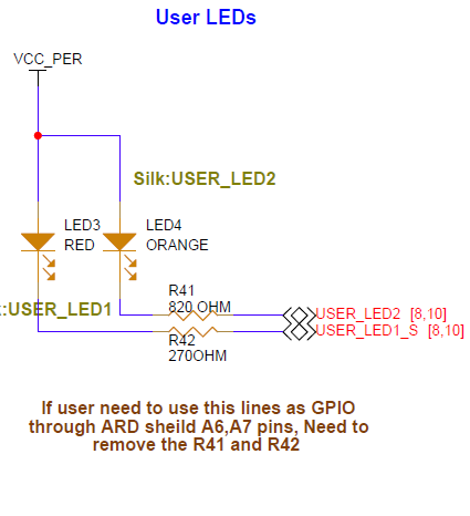
LEDs
There are two onboard user LEDs on the kit. P1.1 and P5.2 to control the LED3 and LED4, respectively. The LEDs can be enabled or disabled using the resistors R41 and R42.
Figure 25. LED circuit
Push buttons
CYW920829M2EVK-02 has one reset and two user buttons. See the Device reset section for details on the reset button. User button1 (SW2) is connected to pin P0.5 of the CYW20829 device, which can work in Deep Sleep mode. User button2(SW4) is connected to pin P1.0 of the CYW20829 device.
Figure 26. Push buttons
Digital microphone (DMIC)
A DMIC is provided on the baseboard, is interfaced with the CYW20829 device through the dedicated PDM interface and powered from the VCC_PER rail. SELECT pin on each microphone is biased such that data gives either a HIGH or LOW of the clock signal. You can use this DMIC to execute the voice remote code example in the kit.
Figure 27. DMIC circuit
Analog microphone (AMIC)
An analog MEMS microphone is provided on the baseboard for analog audio application. Differential output AMIC is interfaced with the CYW20829 device through the dedicated analog microphone input pin and AGND pin. This AMIC is powered by the MIC_BIAS rail from the CYW20829 device. You can use this AMIC to execute the voice remote code example in the kit.
Figure 28. AMIC circuit
RGB LED
An RGB LED is available in the baseboard which is controlled through dedicated three digital GPIOs. The three GPIOs are driven from CYW20829 silicon to drive the RGB LED. Port 0.2, Port 0.3, and Port 0.4 are used for red, green, and blue LEDs. Power supply is provided from VCC_PER rail and series current limiting resister is given according to the bias current of 5 mA.
Figure 29. RGB LED circuit
10-pin SWD header
A 10-pin (50 mil pitch) SWD header is provided for the proramming and debugging of the target CYW20829 device using an external programmer such as MiniProg4.
VDDIO (3V3/3V/1V8) will be supplied from the onboard LDO via reverse protection circuit to restrict Kit operation by programmer power.
Figure 30. 10-pin SWD programming/Debug header
Arduino-compatible and extended headers
The baseboard supports generic Arduino-compatible Uno shields and selected Infineon custom defines Arduino-compatible shields. All CYW20829 GPIO pins are brought out to Arduino-compatible headers. Some pins with fixed functions are also multiplexed through 0 Ω or Jumper and connected to headers.
The I/O headers J1-J4, whose position and pin map comply with the Arduino-compatible UNO R3 kit to support Arduino-compatible shields. The system power signals are brought to the pins of J1.
The power supply pins for Arduino-compatible VCC_ARD_3V3 and VCC_ARD_5V0 connect to VCC_3V3 and KP_VBUS through reverse voltage protection circuits.
All GPIOs of the CYW20829 device are at 3V3/3 V/1V8 level based on the selected jumper position in VDDIO power selection. To establish compatibility with the existing Arduino shields, all GPIOs are level mapped with the same VDDIO in the baseboard.
Figure 31. Arduino-compatible and extended headers
CYW20829 device I/O mapping
Table 17 maps the CYW20829 device I/Os to headers and sensors on the baseboard. It also lists the carrier module interface definition.
Table 17. Carrier module interface and pin connections
Carrier module pin | Carrier module pin name | CYW20829 pin | Baseboard connection 1 | Baseboard connection 2 | Baseboard connection 3 |
|---|---|---|---|---|---|
1 | GND | GND | GND | – | – |
2 | VPA_BASE | VDDD | VDDPA | J12.2 | – |
3 | NC | NC | NC | – | |
4 | VPA_BASE | VDDD | VDDPA | J12.2 | – |
5 | NC | NC | NC | – | |
6 | USER_LED1 | P1.1 | USER_LED1 | LED3 | J18.1 |
7 | GND | GND | GND | – | – |
8 | ARD_D18 | P0.2 | GPIO1 | LED5.1 | J18.4 |
9 | ARD_D13_SPI_CLK | P0.4 | ARD_D13 | LED5.4 | J18.6 |
10 | ARD_D19 | P0.3 | GPIO2 | LED5.3 | J18.5 |
11 | ARD_D8 | P1.5 | ARD_D8 | J3.1 | – |
12 | ARD_D6_PDM_CLK | P0.0 | ARD_D6_PDM_CLK | U11.3 | J2.5 |
13 | NC | NC | NC | – | – |
14 | ARD_D7_PDM_DATA | P0.1 | ARD_D7_PDM_DATA | U11.1 | J2.6 |
15 | NC | NC | NC | – | – |
16 | USER_LED2 | P5.2 | USER_LED2 | LED4 | J18.2 |
17 | ARD_A0/Thermistor | P3.4 | ARD_A0/Thermistor | J14.1 | J2.1 |
18 | GND | GND | GND | – | – |
19 | ARD_A1 | P3.5 | ARD_A1 | J2.1 | – |
20 | NC | NC | NC | – | – |
21 | ARD_D10_SPI_CS | P5.1 | CAN_FD_TX | J2.8 | – |
22 | BT_UART_TXD | P3.3 | BT_UART_TXD | U5_P12.7 | – |
23 | ARD_D2 | P1.4 | ARD_D2 | J4.3 | – |
32 | BT_UART_RXD | P3.2 | BT_UART_RXD | U5_P12.6 | – |
33 | RSVD_10 | P2.5 | SMIF_SPI_CLK | U14.6 | – |
34 | BT_UART_RTS | P3.1 | BT_UART_RTS | U5_P15.5 | – |
35 | ARD_D4_SWDCLK | P1.3 | ARD_D4_SWDCLK | U5_P12.3 | J4.5 |
36 | BT_UART_CTS | P3.0 | BT_UART_CTS | U5_P1.6 | – |
37 | ARD_D5_SWDIO | P1.2 | ARD_D5_SWDIO | U5_P12.2 | J4.6 |
38 | ARD_D3_USER_BUTTON2 | P1.0 | ARD_D3_USER_BUTTON2 | SW4 | J4.4 |
39 | GND | GND | GND | – | – |
40 | ARD_D9 | P1.6 | ARD_D9 | J3.2 | – |
41 | NC | NC | NC | – | |
42 | VCC_2V5 | VDD2P5 | VCC_2V5 | U4.1 | J17.3 |
43 | NC | NC | NC | – | |
44 | NC | NC | NC | – | – |
45 | GND | GND | GND | – | – |
46 | NC | NC | NC | – | – |
47 | MIC_P | MIC_P | MIC_P | U13.1 | – |
48 | NC | NC | NC | – | – |
49 | MIC_N | MIC_N | MIC_N | U13.3 | – |
50 | EXT_LPO | P5.0 | LPO_OUT | J2.7 | – |
51 | GND | GND | GND | – | – |
52 | NC | NC | NC | – | – |
53 | MIC_BIAS | MIC_BIAS | MIC_BIAS | U13.2 | – |
54 | RST_N | XRES | BT_RST_N | SW1 | U5_P12.4 |
55 | NC | NC | NC | – | – |
56 | RSVD_9 | P2.0 | SMIF_SPI_SELECT | U14.1 | – |
57 | GND | GND | GND | – | – |
58 | I2C_SDA/SPI_MISO | P4.1 | I2C_SDA_S | U5_15.2 | J3.9 |
59 | RSVD_2 | P2.2 | SMIF_SPI_DATA2 | J12.2 | – |
60 | I2C_SCL/SPI_MOSI | P4.0 | I2C_SCL_S | U5_15.1 | J3.10 |
61 | USER_BUTTON1 | P0.5 | USER_BUTTON1 | SW2 | J18.3 |
62 | NC | NC | NC | – | – |
63 | NC | NC | NC | – | – |
64 | VIO_BASE | VDDIO | VDDIOM2 | J17.2 | – |
65 | ARD_A3 | P3.7 | ARD_A3 | J2.4 | – |
66 | RSVD_7 | P2.3 | SMIF_SPI_DATA1 | U14.2 | – |
67 | ARD_A2 | P3.6 | ARD_A2 | J2.3 | – |
68 | RSVD_6 | P2.4 | SMIF_SPI_DATA0 | U14.5 | – |
69 | GND | GND | GND | – | – |
70 | RSVD_5 | P2.1 | SMIF_SPI_DATA3 | U14.7 | – |
71 | NC | NC | NC | – | – |
72 | VBAT | VBAT | VBAT | J9.3 | – |
73 | NC | NC | NC | – | – |
74 | VBAT | VBAT | VBAT | J9.3 | – |
75 | GND | GND | GND | – | – |
Kit rework
External LPO selection
By default, the P5.0 connects to CAN_RX via R99; remove it and install R55 to use LPO_OUT.
Mount Y1 and C88 to install the baseboard LPO.
Figure 32. 32.768-kHz external LPO oscillator

SMIF interface for baseboard flash
The kit is provisioned with an optional QSPI SMIF-based flash in the baseboard. To isolate the default flash available in the M.2 board and use the optional baseboard flash, a rework is needed in the kit. SMIF memory interface I/Os are shared between SMIF QSPI flash of the baseboard and the M.2 board flash.
To perform the necessary rework on the board by removing or adding the corresponding 0-Ω resistors to work with baseboard SMIF memory modules. See Table 18 for resistor rework details for SMIF.
Table 18. Dual Pmod header and M.2 connector interface multiplexing
CYW920829M2IPA2 M.2 board function | Baseboard | CYW20829 pin | ||
|---|---|---|---|---|
SMIF interface to QSPI flash in baseboard | SMIF interface to QSPI flash in M.2 board | SMIF interface to QSPI flash in baseboard | ||
R14 position B* | R14 position A | Mount (U14, R119, R120, R121, R122, R123, R124, R59, R60, R61, R62, R63, R64, C85) * | P2.3 | |
R15 position B* | R15 position A | P2.4 | ||
R16 position B* | R16 position A | P2.5 | ||
R17 position B* | R17 position A | P2.0 | ||
R18 position B* | R18 position A | P2.2 | ||
R19 position B* | R19 position A | P2.1 | ||
*: Not connected by default.
Figure 33. SMIF memory interface in baseboard
Figure 34. Mounting option to select SMIF memory and M.2 board flash (available in M.2 board)

UART interface on headers compatible with Arduino-standard
UART interface signals are connected between the PSoC™ 5LP device and CYW20829. The same signals have been shared across digital interface connectors compatible with Arduino J4.1–J4.2. For using UART lines on a connector compatible with Arduino, perform the board rework with the specific resistor assembly.
Baseboard | CYW20829 pin | |
|---|---|---|
UART interface to Kitprog3 | UART interface to Arduino shield/extended header | --- |
R34 | R33* | BT_UART_RXD |
R36 | R38* | BT_UART_TXD |
R107 | R106* | BT_UART_CTS |
R108 | R109* | BT_UART_RTS |
*: Not connected by default.
Figure 35. UART signals mounting option
SPI interface selection
The default SPI lines are not configured in the kit. To enable the SPI option and route to the Arduino shield by following the rework.
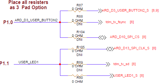
- Default P1.0 is connected to USER_BTN2 via R87, remove it and install R104 to use SPI_CS
- Default P1.1 is connected to USER_LED1 via R90, remove it and install R105 to use SPI_CLK
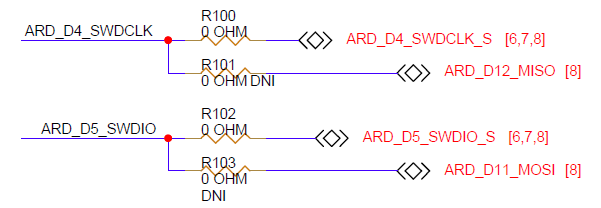
- Default D4 is connected to SWDCLK via R100, remove it and install R101 to use SPI_MISO
- Default D5 is connected to SWDIO via R102, remove it and install R103 to use SPI_MOSI
Figure 36. SPI interface selection
I2S interface selection
The default I2S lines are not configured in the kit. To enable the I2S interface and route to the Arduino shield by following the rework.
- Default P0.4, P3.2 is connected to RGB LED, UART_RX via R83, R95 remove these and install R84, R96 to use I2S_MCLK
- Default P0.5, P3.3 is connected to USER_BTN1, UART_TX via R86, R98 remove these and install R85, R97 to use I2S_TX_SCK
- Default P1.0, P1.4 is connected to USER_BTN2, D2 via R87, R91 remove it and install R88, R92 to use I2S_TX_WS
- Default P1.1, P1.4 is connected to USER_LED1, USER_BTN2 via R90, R94 remove these and install R89, R93 to use I2S_TX_DATA
Figure 37. I2S interface selection


IMU interrupt signal selection
On the kit, the default connection is made for the RGB LED interface. To use the IMU INT1 signal, remove R117 and install R48 to use the CS and INT1 pin of the IMU.
Figure 38. IMU INT1 interface selection

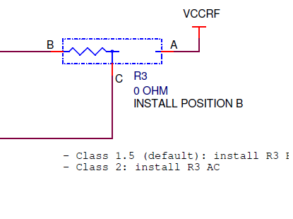
Bluetooth Low Energy TX power selection option
Connect the following pins via 0-Ω resistors on CYW920829M2IPA2 to change the output power level from Bluetooth® Low Energy TX path.
- Default R3 is connected at position BC to use TX10, for TX0 connect R3 at position AC
- TX10 indicates 10 dBm output from CYW20829
- TX0 indicates 0 dBm output from CYW20829
- You can configure to optimize the power consumption and TX output power using this selection option
Figure 39. Bluetooth® Low Energy TX power selection option
Bluetooth External Antenna selection option
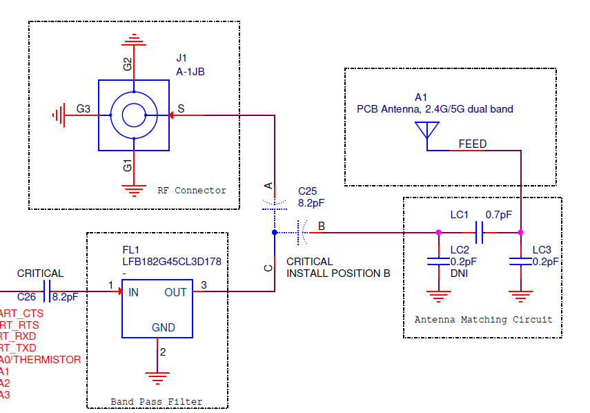
Connect the C25 capacitor on CYW920829M2IPA2 with position A to change the RF IO port to external antenna.
Default C25 is connected at position BC to use onboard PCB antenna. For external antenna, connect C25 at position AC.
Figure 40. Bluetooth® external antenna selection option
Frequently asked questions
- How can I access the SPI (MOSI, MISO) signals that are shared with SWDCLK and SWDIO GPIOs?
- P1.2 is used for ARD_D5_SWDIO and ARD_D11_MOSI in the kit
- P1.3 is used for ARD_D5_SWDCLK and ARD_D12_MISO in the kit
By default P1.2 and P1.3 are connected via R100 and R102 to use as SWD ports in the kit. Therefore, connect the R101 and R103 via 0 Ω resistors on CYW9BTM2BASE3 to use P1.2 and P1.3 as SPI lines: ARD_D11_MISO and ARD_D11_MOSI
- How can I access the SPI (CS, CLK) signals that are shared with User Button2 and USER LED1?
- P1.0 is used for ARD_D3_USER_BUTTON2_S and ARD_D10_SPI_CS in the kit
- P1.1 is used for ARD_D13_SPI_CLK_S and USER_LED1_S in the kit
By default, P1.0 is connected to USER_BTN2 via R87; remove it and install R104 to use SPI_CS. Similarly, P1.1 is connected to USER_LED1 via R90; remove it and install R105 to use SPI_CLK.
- A secondary UART using SCB1 is not connected via KitProg3. How can I access this UART?
P1.2 and P1.3 ports operate as a secondary UART; the TX and RX lines of this UART are available in J4.5 and J4.6. To use SCB1 UART, connect the UART lines from Arduino-compatible shield pins D4 and D5 to MiniProg4 or FTDI.
- SCB2 I2C (P5.0, P5.1) pins are not working as I2C master?
-
Resistor pull-ups are not given, as the same pins are used for CANFD by default
-
Follow any one of the methods to make SCB2 work as a master
- You can use the SCB0 I2C pins (P4.0, P4.1) as master and loop back the SCB2 I2C pins (P5.0, P5.1)
- HAL: Connect external pull-up resistors
- PDL: Enable the SCB from the device configurator and change the pin drive mode from “open drain, drives low, input buffer on” to “resistive pull-up, input buffer on”
- How do I use the EXT_LPO in the kit?
- There is a mismatch of EXT_LPO pin connection in the kit. EXT_LPO is connected to P5.0(WCO_IN); but it has to be connected to P5.1(WCO_OUT)
- PILO is used as the default clock source; in case to use an external crystal oscillator, rework the following tripad resistors on the M.2 board CYW920829M2IPA2:
- R31: Remove the resistor from option AC and install it at position BC
- R30: Remove the resistor from option AC and install it at position BC
- R6: Remove the resistor from the M.2 Board
- Why can’t we use P1_0, P1_1, P1_2, and P1_3 during DS RAM mode of operation?
When the device is in DS-RAM mode, the following pins are utilized for SWD operation:
- P1_0_CPUSS_SWJ_SWO_TDO
- P1_1_CPUSS_SWJ_SWDOE_TDI
- P1_2_CPUSS_SWJ_SWDIO_TMS
- P1_3_CPUSS_CLK_SWJ_SWCLK_TCLK
To utilize these pins, disable debug mode before the device enters DS-RAM mode by using Cy_Syslib_SetWarmBootEntryPoint() API. To disable debug mode in DS-RAM, the second parameter in the API must be set to ‘False’
If the debug mode is disabled, the evaluation kit cannot be programmed. To re-program the device, use the make erase command on modus shell
- Why is VDDIO current greater than 2 µA in DS and DS-RAM during current measurement?
Remove the resistors R12 and R13 from CYW920829M2IPA2. Configure the RTS and CTS pins to an analog High-Z state before entering the Deep Sleep/Deep Sleep-RAM, and after waking up, reconfigured to their original state.
- What do I need to do if I2C and SPI don’t operate when we provide power using a coin-cell for Master and Slave devices?
- Since the KitProg 3 section is not powered ON, the current is sinking into the KitProg 3 internal ESD diodes
- For I2C, resistors R31 and R32, which are connected to KitProg3, must be isolated on the Master side
- For SPI, resistors R56 and R57, which are connected to SWDCLK and SWDIO, must be isolated on the Master side
References
Note: This user manual should be read in conjunction with the following documents available at CYW20829 Product page:
- Infineon Technologies AG: Code examples: Infineon GitHub repository; Available online
- Infineon Technologies AG: Datasheet: CYW20829, AIROC™ Bluetooth® LE 5.4 MCU; Available online
- Infineon Technologies AG: Eclipse IDE for ModusToolbox™ user guide; Available online
Glossary
API
Application Programming Interface EVK
Evaluation Kit GPIO
General Purpose Input/Output HCI
Host Controller Interface I2C
Inter-Integrated Circuit IDE
Integrated Development Environment JTAG
Joint Test Action Group LE
Low Energy LED
Light emitting diode LPO
Low-power oscillator MEMS
Micro electro-mechanical system NTC
Negative Temperature Coefficient PCB
Printed Circuit Board SPI
Serial Peripheral Interface SWD
Serial Wire Debug UART
Universal Asynchronous Receiver/Transmitter USB
Universal Serial Bus XTAL
Crystal oscillator
Revision history
Document revision | Date | Description of changes |
|---|---|---|
** | 2023-05-31 | Initial release. |
*A | 2023-08-25 | Updated figures and tables in Kit operation. Added FAQ section. |
*B | 2024-04-12 | Updated template; no content update |