AN215656 PSoC™ 6 MCU dual-core system design
About this document
Scope and purpose
AN215656 describes the dual-core architecture in PSoC™ 6 MCUs, which includes Arm® Cortex®-M4 and Cortex®-M0+ cores, as well as an inter-processor communication (IPC) module. A dual-core architecture provides the flexibility to help improve system performance and efficiency and reduce power consumption. The application note also shows how to build a simple dual-core design using ModusToolbox™ software, Command-line Interface (CLI), and PSoC™ Creator IDE, and how to debug the design using various IDEs.
To access an ever-growing list of hundreds of PSoC™ code examples, please visit our code examples web page. You can also explore the Infineon video training library here.
Intended audience
This application note is intended for advanced engineers who want to use the full dual-core capabilities of the PSoC™ 6 MCU.
Introduction
PSoC™ 6 MCU is 32-bit ultra-low-power PSoC™, purpose-built for the Internet of Things (IoT). It integrates low-power flash and SRAM technology, programmable digital logic, programmable analog, high-performance analog-digital conversion, low-power comparators, and standard communication and timing peripherals.
Of particular interest in PSoC™ 6 MCU is the CPU subsystem. The architecture incorporates multiple bus masters – two CPUs, DMA Controllers, and a cryptography block (Crypto) – as Figure 1 shows:

Generally, all memory and peripherals are shared by all bus masters. Shared resources are accessed through standard Arm multi-layer bus arbitration. Exclusive accesses are supported by an inter-processor communication (IPC) block, which implements semaphores and mutual exclusion (mutexes) in hardware.
A dual-core architecture, along with the DMA and cryptography (Crypto) bus masters, presents unique opportunities for system-level design and performance optimization in a single MCU. With two CPUs you can:
- Allocate tasks to CPUs so that multiple tasks may be done at the same time.
- Allocate resources to CPUs so that a CPU may be dedicated to managing those resources, improving efficiency.
- Enable and disable CPUs to minimize power draw.
- Send data between the CPUs using the IPC block. For more information, see the code example mtb-example-psoc6-dual-cpu-ipc-pipes.
In one example application, the Cortex®-M0+ CPU (CM0+) can “own” and manage all communication channels. The Cortex®-M4 CPU (CM4) can send and receive messages from the channels via CM0+. This frees CM4 to do other tasks while CM0+ manages the communication details.
Tools and libraries
Infineon provides two development platforms that you can use for application development with PSoC™ 6 MCU:
- ModusToolbox™: ModusToolbox™ cross platform software includes configuration tools, low-level drivers, middleware libraries, and operating system support, as well as other packages that enable you to create MCU and wireless applications. It also includes the optional Eclipse IDE for ModusToolbox™.
- PSoC™ Creator: A Infineon-proprietary IDE that runs on Windows only. It supports a subset of PSoC™ 6 MCU devices as well as other PSoC™ device families such as PSoC™ 3, PSoC™ 4, and PSoC™ 5LP.
Both platforms provide a mechanism to load and run applications in third-party tools, such as Keil µVision, IAR Embedded Workbench and Visual Studio Code.
Infineon also provides a set of libraries to facilitate application development with PSoC™ 6 MCU:
- Peripheral Driver Library (PDL): PDL drivers abstract hardware functions into a set of easy to use APIs. For more information on the PDL, go to the mtb-pdl-cat1 webpage. This library is available in PSoC™ Creator and ModusToolbox™ software.
- Hardware Abstraction Layer (HAL): HAL is built on top of the PDL. It provides a high-level interface to configure and use hardware blocks on Infineon MCUs. It is a generic interface that can be used across multiple product families. For more information on the HAL, go to the mtb-hal-cat1 webpage. The HAL is available only in ModusToolbox™ software. PSoC™ Creator does not have support for HAL.
- Middleware: This category includes multiple libraries that implement APIs for various domains, capacitive sensing is one such example. A middleware library may be created by Infineon or come from a third party. In PSoC™ Creator, the middleware is usually available as a PSoC™ Creator Component. In ModusToolbox™ software, it is available as a library.
- Board Support Package (BSP): BSP provides a standard interface to a board’s features and capabilities. The API is consistent across Infineon kits. Other software (such as middleware or an application) can use the BSP to configure and control the hardware. The BSP is available in ModusToolbox™ software only. Although PSoC™ Creator does not offer BSP, you can install the kit software, allowing you to start a new project based on the selected kit.
How to use this document
This document assumes that you are familiar with PSoC™ 6 MCU architecture, and application development for PSoC™ devices using either ModusToolbox™ software or PSoC™ Creator IDE. For an introduction to PSoC™ 6 MCU, see the following:
A PSoC™ 6 MCU device datasheet
- AN228571 - Getting Started with PSoC™ 6 MCU on ModusToolbox™ software
- AN221774 - Getting Started with PSoC™ 6 MCU on PSoC™ Creator
- AN210781 - Getting Started with PSoC™ 6 MCU with Bluetooth® low energy connectivity on PSoC™ Creator
If you are new to ModusToolbox™ software, see the ModusToolbox™ software home page. Some PSoC™ 6 MCU devices are not supported by PSoC™ Creator; in this case, ModusToolbox™ software must be used. If you are using ModusToolbox™ software, make sure that it’s version 3.0 or higher for designs based on PSoC™ 6 MCU devices with dual CPUs.
If you are new to PSoC™ Creator, see the PSoC ™ Creator home page. Use PSoC™ Creator version 4.3 or higher for PSoC™ 6 MCU-based designs.
General dual-core concepts
The process of developing firmware for a dual-core MCU is similar to that for a single-core MCU, except that you write code for two CPUs instead of one. You should also consider any need for inter-processor communication.
Performance: The main advantage of having two CPUs is that you essentially multiply your CPU power and bandwidth. How to use that increased bandwidth depends on the tasks that your application must perform.
Single task: A single-task application may be less of a fit for a dual-core MCU unless the application is large and complex. In PSoC™ 6 MCU, you can execute the task on one of the CPUs and put the other CPU to sleep to reduce power.
Dual task: This is the most obvious fit; assign each task to a CPU. Assign the task with larger computing requirements to the higher-performance CPU, i.e., Cortex®-M4 in PSoC™ 6 MCU.
Multiple tasks: Again, assign each task to a CPU. In each CPU, you must include a method for executing each task in a timely fashion.
RTOS: A complex multitasking system may be managed by a real-time operating system (RTOS). An RTOS basically allocates a number of CPU cycles to each task, depending on the task priority or whether a task is waiting for an event. You effectively do that yourself by assigning tasks to the CPUs. Some examples of dual-core RTOS architectures are:
- Each CPU has its own RTOS and its own set of tasks. Each RTOS should include a task to manage communications with the other CPU.
- Only one CPU has an RTOS and multiple tasks. The other CPU is idle until it is messaged to do a specified task. It then wakes up and does the task, then messages the result back to the first CPU. As an example, the lower-performance CPU, CM0+ in PSoC™ 6 MCU, can use the higher-performance CPU, CM4 in PSoC™ 6 MCU, to do computation-intensive tasks when needed.
- Power: In a dual-core system, firmware can start and stop the CPUs to fine-tune power usage. In the previous example, to reduce power, the high-performance CPU is placed into a sleep state until needed for a computation-intensive task.
- Debug: Debugging two bodies of code at the same time may be a complex process. Usually you debug code for one CPU, then debug code for the other CPU. In addition, a device such as an oscilloscope or a logic analyzer may be useful for monitoring communication between the CPUs.
PSoC 6 MCU dual-core architecture
Figure 1 shows the overall dual-core architecture in PSoC™ 6 MCU. (For detailed block diagrams of PSoC™ 6 MCU, see the device datasheet) Specific features and other details related to dual CPUs are listed in this section. For more information, see the ARM® documentation sets for Cortex® - M4 and Cortex® -M0+, and the PSoC™ device technical reference manual (TRM).
CPUs: Both CPUs –Cortex® M4 and Cortex® M0+ – are 32-bit. CM4 runs at up to 150 MHz and has a floating-point unit (FPU). CM0+ runs at up to 100 MHz.
CM4 is the main CPU. It is designed for a short interrupt response time, high code density, and high throughput. The CM0+ CPU is secondary; it is used in PSoC™ 6 MCU to implement system calls and device-level security, safety, and protection features. CM0+ is also recommended for functions such as Bluetooth® LE communications and CAPSENSE™.
Performance: CM0+ typically operates at a slower clock speed than CM4. The CM0+ instruction set is more limited than that of CM4. Therefore, it may require more cycles to implement a function on CM0+, and the cycle time is longer. Keep this in mind when deciding to which CPU to allocate tasks.
Security: PSoC™ 6 MCU has several security features; see the TRM for details. To meet security requirements, CM0+ is used as a "secure CPU". It is considered to be a trusted entity; it executes Infineon system code and application code. The use of CM0+ for system and security tasks may limit its availability for applications. For more information, on secure systems, see AN221111 - PSoC™ 6 MCU designing a custom secured system.
Device system calls may be initiated by either CPU but are always executed by CM0+.
Startup sequence: After device reset, only CM0+ executes; CM4 is held in a reset state. CM0+ first executes Infineon system and security code, including SROM code, FlashBoot, and Secure Image. For more information on these code modules, see the Boot Code chapter of the Architecture TRM for details.
After CM0+ executes the system and security code, it executes the application code. In the application code, CM0+ may release the CM4 reset, causing CM4 to start executing its application code. PSoC™ Creator auto-generates code in CM0+ main() to release the CM4 reset. In ModusToolbox™ software, the BSP chooses and includes one of the several available CM0+ prebuilt images.
Inter-processor communication (IPC): IPC enables the CPUs to communicate and synchronize activities. The IPC hardware contains register structures for IPC channel functions and IPC interrupts. IPC channel registers implement mutual exclusion (mutex) lock/release mechanisms, and messaging between the CPUs. IPC interrupt registers generate interrupts to both CPUs for messaging events and lock/release events.
Interrupts: Each CPU has its own set of interrupts. All peripheral interrupt lines are hard-wired to specific CM4 interrupt inputs. Peripheral interrupts are also multiplexed to CM0+’s limited set of 8 interrupt inputs (32 interrupt inputs in the CY8C61x7, CY8C62x7, and CY8C63x7). See Interrupt Assignment Considerations.
Power modes: PSoC™ 6 MCU has several power modes that can affect either the entire system or just a single CPU. CPU power modes are Active, Sleep, and Deep Sleep as defined by Arm®. Device system power modes are LP, ULP, Deep Sleep, and Hibernate.
- System Low Power (LP) mode is the default operating mode of the device after reset. It provides the maximum performance. While in System LP mode, the CPUs may operate in any of the Arm®-defined modes.
- System Ultra Low Power (ULP) mode is identical to LP mode with a performance tradeoff made to achieve a lower system current. This tradeoff lowers the core operating voltage, which then requires a reduced operating clock frequency, and limited high-frequency clock sources. While in system ULP mode, the CPUs may operate in any of the Arm®-defined modes.
- In System Deep Sleep mode, all high-speed clock sources are OFF. This in turn stops both CPUs and makes high-speed peripherals unusable. However, low-speed clock sources and peripherals continue to operate, if configured and enabled by the firmware. Interrupts from these peripherals cause the device to return to System LP or ULP mode and one or more CPUs to wake up to Active mode. Each CPU has a Wakeup Interrupt Controller (WIC) to wake up the CPU.
- System Hibernate mode is the lowest power mode of the device. It is intended for applications that may go into a dormant state. The device goes through a reset on wakeup from Hibernate. See Startup sequence.
- In CPU Active mode, the CPU executes code and all logic and memory is powered. The device must be in System LP or ULP mode.
- In CPU Sleep mode, the CPU clock is turned OFF and the CPU halts code execution. The device must be in System LP or ULP mode.
- In CPU Deep Sleep mode, the CPU requests the device to go into System Deep Sleep mode. When the device is ready, it enters System Deep Sleep mode. In PSoC™ 6 MCU, both CPUs must enter CPU Deep Sleep before the system transitions to Deep Sleep. If only one CPU has entered CPU Deep Sleep mode, the system remains in LP or ULP mode.
- For more information on PSoC™ 6 MCU power modes, see AN219528 - PSoC™ 6 MCU low-power modes and power reduction techniques.
Debug: PSoC™ 6 MCU has a Debug Access Port (DAP) that acts as the interface for device programming and debug. An external programmer or debugger (the "host") communicates with the DAP through the device Serial Wire Debug (SWD) or Joint Test Action Group (JTAG) interface pins. Through the DAP (and subject to device security restrictions), the host can access the device memory and peripherals as well as the registers in both CPUs.
Each CPU offers several debug and trace features as follows:
- CM4 supports six hardware breakpoints and four watchpoints, 4-bit embedded trace macrocell (ETM), serial wire viewer (SWV), and printf()-style debugging through the single-wire output (SWO) pin.
- CM0+ supports four hardware breakpoints and two watchpoints, and a micro trace buffer (MTB) with 4 KB dedicated RAM.
PSoC™ 6 MCU also has an Embedded Cross Trigger for synchronized debugging and tracing of both CPUs.
Some third-party IDEs support synchronized dual-core debugging; see Debug considerations. Infineon's ModusToolbox™ software supports dual-core debugging (unsynchronized), and PSoC™ Creator supports debugging a single CPU (either CM4 or CM0+) at a time.
PSoC 6 MCU dual-core development
This section shows only those development aspects that are unique to PSoC™ 6 MCU dual-core devices. To learn more about PSoC™ 6 MCU, ModusToolbox™ software, or PSoC™ Creator, see one or more of the following:
- AN228571 - Getting Started with PSoC™ 6 MCU on ModusToolbox™ software
- AN221774 - Getting Started with PSoC™ 6 MCU on PSoC™ Creator
- AN210781 - Getting Started with PSoC™ 6 MCU with Bluetooth® low energy connectivity on PSoC™ Creator
- The ModusToolbox™ software home page. Some PSoC™ 6 MCU devices are not supported by PSoC™ Creator; in this case, ModusToolbox™ software must be used. If you are using ModusToolbox™ software, then make sure it’s version 3.0 or higher for designs based on PSoC™ 6 MCU devices with dual CPUs
- The PSoC ™ Creator home page. Use PSoC™ Creator version 4.3 or higher for PSoC™ 6 MCU-based designs
ModusToolbox software instructions
ModusToolbox™ software application development for a PSoC™ 6 MCU dual-core device is similar to that for any other device supported by ModusToolbox™ software. By default, the Board Support Packages (BSP) that come with the ModusToolbox™ software provides several prebuilt CM0+ application images. This section explains how to create your own CM0+ application as a substitute for the prebuilt images.
To create a dual-core application, you can follow one of the following methods:
- If you are starting dual-core application development from scratch, you can create your new application based on an existing dual-CPU code example hosted here. You can use any code example with a repo name that includes “dual-CPU” as a start point. For most cases, the mtb-example-psoc6-dual-cpu-empty-app is a good choice.
- If you have an existing single-core application that you want to convert to a dual-core application, follow the steps from Creating a dual-core application section.
Creating a dual-core application
This section shows how to create a dual-core application step-by-step by using an existing single-core application and a starter dual-core application. Here the starter dual-core application will act as a template defining the dual-core application structure. The existing single-core application's contents can easily be copied into the starter dual-core application.
For the single-core application, as an example, the mtb-example-psoc6-hello-world is chosen. For the starter dual-core application, the mtb-example-psoc6-dual-cpu-empty-app is chosen. The CY8CPROTO-062S2-43439 BSP is chosen for both applications.
The applications can be created using one of the following methods:
Eclipse IDE for ModusToolbox™
Launch Eclipse IDE for ModusToolbox™ 3.0 or later and select a workspace.
From the Quick Panel, click New Application.
Once the project creator wizard opens, expand PSoC™ 6 BSPs and select CY8CPROTO-062S2-43439. Click Next.
In the new window, expand Getting Started, select Dual-CPU Empty PSoC6 App and Hello World. Click Create.
In Figure 2 , you see both applications created in the workspace.
Figure 2. Workspace in ModusToolbox™ containing both single-core and dual-core applications 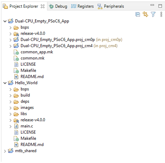
Command-line Interface (CLI)
For project creation, open a CLI terminal and navigate to ModusToolbox™ software installation folder such as <install_path>/ModusToolbox/tools_<version>/project-creator/.
Create both the applications by executing the following
project-creator-clicommands.project-creator-cli \
--board-id CY8CPROTO-062S2-43439 \
--app-id mtb-example-psoc6-hello-world \
--user-app-name Hello_World \
--target-dir "C:/workspace_directory"project-creator-cli \
--board-id CY8CPROTO-062S2-43439 \
--app-id mtb-example-psoc6-dual-cpu-empty-app \
--user-app-name Dual-CPU_Empty_PSoC6_App \
--target-dir "C:/workspace_directory"
Alternatively, you can execute the project-creator tool in the same folder and follow the same steps described in Eclipse IDE for ModusToolbox™.
For more information, see Section 2.3 in the ModusToolbox™ user guide.
Modify application contents
The following contents from the Hello World example need to be selectively
copied to the CM4 project (proj_cm4) of the Dual CPU Empty
application:
Makefile variables – Open the Makefile of the Hello World application and
proj_cm4application side-by-side. Compare and copy the variable values from the Hello World Makefile to theproj_cm4Makefile. If some of the variables defined in the Hello World Makefile are not present in theproj_cm4Makefile, they should be available in the common.mk and common_app.mk Makefiles at the root level of the dual-core empty application.Current values of variables such as
MTB_TYPE,APPNAME,COMPONENTS, andDISABLE_COMPONENTSin the Dual CPU Empty application Makefiles should not be deleted or modified. Adding new values is still allowed for variables such asCOMPONENTSandDISABLE_COMPONENTS.For the Hello World application case, there are no Makefile variables that need to be copied.
Source files – Replace all the source files from the
proj_cm4application with the Hello World application.Libraries/Middleware – The libraries or middleware used in the Hello World application should also be added to the
proj_cm4application. Follow these steps to add them:- In the Eclipse IDE of ModusToolbox™, from the quick planel launch Library Manager tool. Alternatively, you can launch the Library Manager from the tools folder of ModusToolbox™ installation directory, in this case the correct path to the Dual CPU Empty application needs to be selected from the Library Manager window.
- Once the Library Manager opens, click Add Library.
- Select Target Project as proj_cm4.
- Under Peripheral, select retarget-io library, and click OK.
- Click Update from the Library Manager window. Wait for the libraries to get added; see the log messages for progress.
- Once the libraries are updated, click Close.
The CM0+ project (proj_cm0p) of the Dual CPU
Empty application enables the CM4 core and goes to Deep Sleep. To use the core for any
other purpose, the cybsp_init() function needs to be called from the
CM0+ core. This function will do all the system-level initialization required to run
peripherals on the CM0+ core. Modify the main.c
file of
proj_cm0p as shown in Code Listing 1.
Code Listing 1
#include "cy_pdl.h"
#include "cycfg.h"
#include "cybsp.h"
int main(void)
(
  cy_rslt_t result;

  /* Initialize the device and board peripherals */
  result = cybsp_init() ;
  if (result != CY_RSLT_SUCCESS)
  (
    CY_ASSERT(0);
  )

  /* Enable global interrupts */
  __enable_irq();

  /* Enable CM4. CY_CORTEX_M4_APPL_ADDR must be updated if CM4 memory layout is changed. */
  Cy_SysEnableCM4(CY_CORTEX_M4_APPL_ADDR);

  for (;;)
  (
    Cy_SysPm_DeepSleep(CY_SYSPM_WAIT_FOR_INTERRUPT);
  )
)
The Infineon HAL is not yet designed to run simultaneously on CM0+ and CM4
core. Since the proj_cm4 already uses HAL,
proj_cm0p should only use PDL APIs.
Build and program
The application can be built and programmed using one of the following methods:
Using Eclipse IDE for ModusToolbox™
- Select the Dual-CPU_Empty_PSoC6_App application from the project explorer.
- From the quick panel, select Dual-CPU_Empty_PSoC6_App Program MultiCore
(KitProg3). This will build and program both projects –
proj_cm0pandproj_cm4, one after the other. - Alternatively, you can program individual projects (
proj_cm0porproj_cm4), but this is only possible through CLI interface as explained below.
Using Command-line Interface (CLI)
Open a modus-shell and navigate it to the root directory of the Dual-CPU_Empty_PSoC6_App application.
Run command - make program. This will build and program both projects –
proj_cm0pandproj_cm4, one after the other.Alternatively, you can program individual projects (
proj_cm0porproj_cm4). Navigate themodus-shellto the required project directory. Run commandmake program_proj.
The build artifacts for each project is generated in its own project directory under a folder named build. Note that the build folder in the application level has a copy of the project hex files. It also has a combined hex file containing the data of individual project hex files.
If the projects fail to build due to a flash overflow error, follow the steps from the Customizing linker scripts section to allocate the required memory for each project.
Customizing linker scripts
The CM0+ and CM4 projects each have their own linker scripts supplied by the BSP. By default, the CM0+ CPU consumes only 8192 [0x2000] bytes of flash and 8192 [0x2000] bytes of SRAM. If your CM0+ project requires more memory, both linker scripts require changes. Note that the increment/decrement in flash size should be in multiples of flash row size (512 bytes). The following steps list the changes:
The CM0+ linker script is located at directory - bsps/TARGET_APP_<BSP_NAME>/COMPONENT_CM0P/
By default, the BSP supports the ARM (.sct), GCC_ARM (.ld), and IAR (*.icf) toolchains. Each toolchain has its own linker script.
Edit the FLASH and SRAM size as desired:
Toolchain: Where to change ARM (*.sct)
#define RAM_SIZE 0x00002000
#define FLASH_SIZE 0x00002000
GCC_ARM (*.ld)
ram (rwx) : ORIGIN = 0x08000000, LENGTH = 0x2000
flash (rx) : ORIGIN = 0x10000000, LENGTH = 0x2000
IAR (*.icf)
define symbol ICFEDIT_region_IRAM1_end = 0x08001FFF;
define symbol ICFEDIT_region_IROM1_end = 0x10001FFF;
The CM4 linker script is located at directory - bsps/TARGET_APP_<BSP_NAME>/COMPONENT_CM4/
Edit the values based on the CM0+ memory size:
Toolchain: Where to change ARM (*.sct)
#define RAM_START 0x08002000
#define RAM_SIZE 0x000FD800
#define FLASH_CM0P_SIZE 0x2000
GCC_ARM (*.ld)
FLASH_CM0P_SIZE = 0x2000;
ram (rwx) : ORIGIN = 0x08002000, LENGTH = 0xFD800
IAR (*.icf)
define symbol ICFEDIT_region_IRAM1_start = 0x08002000;
define symbol ICFEDIT_region_IRAM1_end = 0x080FF7FF;
In the CM0+ Makefile, add to DEFINES the CM4 application address (
CY_CORTEX_M4_APPL_ADDR). For example, if the size of CM0+ image is 0x8000, set it to:DEFINES=CY_CORTEX_M4_APPL_ADDR=0x10008000
Sharing libraries and peripherals
The deps folder of each project contains the list of libraries used by that project. As described earlier ModusToolbox™ provides a tool to manage the libraries and BSPs, called Library Manager. You can launch this tool from the Eclipse IDE for ModusToolbox™, . Alternatively, you can execute the library-manager tool located at this folder: (<install_path>/ModusToolbox/tools_<version>/library-manager/).
The BSPs added through the library manager by default will be downloaded to a folder named bsps located at the root directory of the dual CPU application. Both projects share the BSPs in an application.
The libraries added through the library manager by default will be downloaded to a folder named mtb_shared, located one level above the root directory of the dual CPU application. The libraries can be shared or project-specific. When adding the libraries through the library manager, an option is provided to select the project it belongs to. If the same library is added to both the projects, then both the projects can access the same library copy from the mtb_shared directory.
If a peripheral is shared, you should only initialize it in one of the CPUs and use some sort of mutex orsynchronization mechanism to avoid both CPUs using it at the same time. It is not recommended to use the HAL for shared peripherals, since the CM0+ would not have access to the HAL object created by the CM4.
PSoC Creator instructions
PSoC™ Creator project development for a PSoC™ 6 MCU dual-core device is similar to that for any other device supported by PSoC™ Creator. To create a new project, select File > New > Project. A Create Project dialog is displayed, as shown in Figure 3.

Select Target Device (A), and PSoC 6 (B). On the pull-down list (C), select <Launch Device Selector...> to see a list of PSoC™ 6 devices.
Figure 4 shows the Device Selector dialog. To see a list of dual-core devices, click the CPU category (D) and select only CortexM0p, CortexM4.
In the PSoC™ 6 Bluetooth® LE Pioneer Kit CY8CKIT -062- BLE, the PSoC™ 6 MCU dual-core device part number is CY8C6347BZI-BLD53. In the PSoC™ 6 Wi-Fi Bluetooth® Pioneer Kit CY8CKIT -062- WiFi -BT, the PSoC™ 6 MCU dual-core device part number is CY8C6247BZI-D54.

After selecting a PSoC™ 6 MCU part, the rest of the project creation process is the same as for other devices. Click through the rest of the Create Project dialogs; PSoC™ Creator creates the project.
The initial project windows layout (Figure 5) includes a Workspace Explorer window with the following features for dual-core devices:
- Separate main.c files –
main_cm0p.candmain_cm4.c– for each CPU. Sources in the folders CM0p (Core 0) and CM4 (Core 1) are compiled into separate binaries for the respective CPUs. - A Shared Files folder. Source files in this folder are compiled into both binaries.

The initial project layout also includes a TopDesign hardware schematic, along with an associated component catalog window.
After the project is created, implement your hardware design by dragging Components onto the schematic, and configuring and wiring them.
When schematic design entry is complete, select Build > Generate Application. This creates several system source code files and folders in the existing folders as well as in the new folder Generated Source, as Figure 6 shows.
The generated source contains drivers for each Component on the schematic, as well as Infineon's peripheral driver library (PDL). The PDL is a software development kit (SDK) that integrates device header files, start-up code, and peripheral drivers. The peripheral drivers abstract the hardware functions into a set of easy-to-use APIs.
For more information on the PDL, select PSoC™ Creator Help > Documentation > Peripheral Driver Library. Also, each Component has a datasheet that documents the driver API for that Component. Right-click the Component and select Open Datasheet....
PSoC™ Creator IDE creates several other files and folders, and places them in existing folders CM0p (Core 0), CM4 (Core 1), and Shared Files. These files generally support configuration, start-up, and linking options for PSoC™ Creator as well as other IDEs. For more information on these files, see PSoC™ Creator Help article, Generated Files (PSoC™ 6).

Resource assignment considerations
All PDL driver source and other API files are available to both CPUs. If code for a CPU references any API element in a generated source file, that file is compiled into the binary for that CPU. The same file can be compiled into both binaries – see code example CE216795 , PSoC ™ 6 MCU dual-CPU basics.
Note: Customers using PSoC™ Creator should download the required examples inside the tool using the project creation wizard. The PSoC™ Creator code example links provided in this document point only to the code example document.
If the same source file is compiled into both binaries, a function in that file is duplicated in both binaries. Even though the copies are in separate builds and binaries, in some cases it is convenient to consider a function to be executed simultaneously by both CPUs.
As noted previously, it is possible for a peripheral to be accessed by both CPUs; for example, both CPUs may send data through the same UART.
There are two ways to do resource management:
- Dedicate a resource to one CPU. Include code to use the resource only in the firmware for the desired CPU. Also, if you are using PSoC™ Creator, a good practice is to indicate on the project schematic the CPU that “owns” the resource, as Figure 7 shows

- Share resources between the CPUs. Code example CE216795 shows how the PSoC™ 6 MCU’s IPC block may be used to implement a mutex to share memory between the CPUs. Use the same technique to share a peripheral resource such as a UART
Flash and SRAM that are allocated in a CPU’s binary are generally separate from that for the other CPU. If custom sections and section placement are defined in the CPUs’ linker scripts, you must ensure that the sections do not overlap. Conversely, another way to share memory is to define for each CPU custom sections with the same address.
Power mode transition considerations
Resources such as system clocks are always shared between CPUs and all peripherals. The
cybsp_init() function calls
cybsp_register_sysclk_pm_callback() function. This function registers a
power management callback that prepares the clock system for Deep Sleep mode and
restores the clocks upon wakeup from a Deep Sleep.
The default cybsp_register_sysclk_pm_callback() is designed for single CPU
examples, where CM0+ is in a Deep Sleep. If the CM4 CPU is also put to Deep Sleep, the
callback function disables the clock system. This will not cause any problem to the CM0+
CPU as it is already in a Deep Sleep. In the case of dual CPU examples, this is not the
case. If one of the CPUs goes to Deep Sleep, the callback doesn’t check the state of the
other CPUs and disables the clock system. This causes the other active CPUs to
misbehave.
To avoid the above issue, a custom power management callback function is needed. In this custom callback, you can decide whether to disable the system clocks or not. You can also implement any other custom functions required for your application when performing a power mode transition. See the default callback function implementation to write your custom callback in the correct format.
Follow these steps to create and call a custom power management callback function:
From the root of your dual CPU example, create a shared folder to add source files.
For example: shared/source/
Create a C file with any name.
For example: shared/source/custom_pm_callback.c
Open the file and write a custom callback function with the exact same definition and name as shown below:
cy_rslt_t cybsp_register_custom_sysclk_pm_callback(void)
(
. . .
)
Open the Makefiles of both CM0p and CM4 projects. Make the following changes:
- Edit the SOURCES variable to add the newly created C file to the build
process.
SOURCES= ../shared/source/custom_pm_callback.c
- Add
CYBSP_CUSTOM_SYSCLK_PM_CALLBACKmacro to the DEFINES variable.
- Edit the SOURCES variable to add the newly created C file to the build
process.
IPC configuration considerations
Inter-Process Communication (IPC) provides the functionality for multiple CPUs to communicate and synchronize their activities. Following are some of the guidelines one needs to consider while using IPC:
- The shared memory used for IPC communication can be placed in an
unprotected public RAM region. This
public_ramregion is defined and commented in the defaultCM0+linker script provided by the target BSP. To use this public RAM region, uncomment thepublic_ramline and.cy_sharedmemsection in theCM0+linker script. - The
public_ramregion must be given executable privileges to allow for flash write functions to run out of the SRAM. This can be achived by changing therwparameter torwxparameter in thepublic_ramline of theCM0+linker script. - If the
public_ramregion is not used, the shared memory will be allocated in the SRAM region defined for the CM0+ CPU. - When using protection units, the user application should take care not to protect the shared memory region.
Interrupt assignment considerations
An important consideration for dual-core designs is assigning and handling interrupts. As noted previously, all device interrupts are available to CM4, and a subset of interrupts are routed through multiplexers to CM0+. You must decide which CPU will handle each interrupt.
For more information, see application note AN217666 - PSoC ™ 6 MCU interrupts.
PSoC™ Creator: For PSoC™ Creator, let us assign interrupts in an example design. Figure 8 shows a design
with two interrupts; one from a PWM Component, connected to an Interrupt Component
MyPWM_Int; and the other from an I2C Component.
In the Design wide Resources window (file type .cydwr), select the Interrupts tab to see all of the interrupts in the design, as Figure 9 shows.
In this example, the I2C component has an interrupt embedded in it. That
interrupt is not shown on the schematic in Figure 8; it is shown in the Design-Wide Resources
window as MyI2C_SCB_IRQ.

Check or uncheck the boxes in the Arm® CM0+ Enable and Arm® CM4 Enable columns to assign interrupts to the respective CPUs.

Each peripheral interrupt is hard-wired to CM4, so the Interrupt Number is automatically assigned by PSoC™ Creator when you build the project. Because interrupts are routed through multiplexers to CM0+, you can select an Arm® CM0+ Vector for each interrupt.
Debug considerations
Third-party IDEs such as Keil µVision and IAR Embedded Workbench support dual-core debugging. Eclipse IDE for ModusToolbox™ software supports dual-core debugging (unsynchronized), and PSoC™ Creator supports debugging a single CPU (either CM4 or CM0+) at a time.
ModusToolbox instructions
Eclipse IDE for ModusToolbox™ software supports asynchronous dual core debugging. You can launch the debug session for both cores simultaneously, but debug activites (For example, halt, stop, breakpoints) on one core will not affect the other. For detailed instructions, open the ModusToolbox™ User Guide, and see the subsection PSoC™ 6 MCU Programming/Debugging.
PSoC Creator instructions
PSoC™ Creator supports debugging just one CPU at a time. Before starting a debug session with PSoC™ 6 MCU, select the desired debug target (Debug > Select Debug Target...), as Figure 10 shows. Select the desired CPU and click OK/Connect. To debug the other CPU, you must exit the debugger and then re-enter it with a connection to that CPU.

Recommended: Develop and debug first the portions of code where the CPUs communicate with each other. After that, code executed by an individual CPU can be debugged separately. For example, when the shared memory project in CE216795 was developed, the portion where CM0+ sends an initial message to CM4 was developed and debugged before subsequent portions of code were developed.
You can debug both CPUs simultaneously by using other IDEs such as µVision or IAR. To do so, you must export your PSoC™ Creator project to the other IDE. PSoC™ Creator documents this topic in the help articles Integrating into 3rd Party IDEs, PSoC™ 6 Designs. Review the instructions in the help articles; the general steps are summarized in the following sections.
Instructions for other IDEs
Exporting ModusToolbox applications to supported IDEs
ModusToolbox™ software has a mechanism to load and run applications on the following IDEs:
- IAR Embedded Workbench
- Keil µVision
- Visual Studio Code
For more details on how to export and set up debugging with these tools, see the “Exporting to IDEs” chapter in the ModusToolbox™ user guide.
Exporting from PSoC Creator
If you are using PSoC™ Creator, you can export your project to Keil µVision or IAR Embedded Workbench for dual-core debugging. Following are the steps to do so:
- Configure the PSoC™ Creator Project
- Create µVision Projects
- Debug µVision Projects
- Create IAR-EW Projects
- Debug IAR-EW Projects
- Configure the PSoC™
Creator Project
Update the Target IDEs settings in the project Build Settings, as Figure 11 shows
For µVision, select CMSIS Pack: > Generate. Enter appropriate identifying text for the CMSIS pack in the Vendor, Pack, and Version fields
Recommended: select Toolchain: > ARM MDK Generic
For IAR, you only need to select IAR EW-ARM: > Generate. (An advanced option, Generate without copying PDL files, is also available.) IAR has its own compiler (not supported by PSoC™ Creator), so the Toolchain selection is irrelevant
Figure 11. Build settings for target IDEs 
Then build your PSoC™ Creator project in the usual manner. A folder Export is created in your <project>. cydsn folder, which contains relevant files for exporting to the selected IDE or IDEs
For µVision, after the PSoC™ Creator project is built, find the corresponding .pack file in the folder Export \ Pack. Double-click the file to install it as a µVision pack, as Figure 12 shows.
Note: Do not use the µVision Pack Installer Wizard File Import function to install this pack.Figure 12. Install µVision pack from PSoC™ Creator project 
if you update the PSoC™ Creator project, consider changing the µVision pack version number (see Figure 11) and installing the new pack
For more information, see AN219434 - Importing PSoC™ Creator Code into an IDE for a PSoC™ 6 Project
- Create µVision projects
For µVision, you must create two projects: one for each PSoC™ 6 MCU CPU: CM0+ and CM4. Do the following:
Recommended: create a new folder (For example. µVisionBuild) within your PSoC™ Creator <project>. cydsn folder to store all µVision project files separately from the PSoC™ Creator files (this is different from the IAR instructions). Within that folder, create another new folder for CM4 object files (For example, ObjectsM4), as Figure 13 shows:
Figure 13. New folders for µVision projects 
Open µVision 5.25 or later and create a new project (Project > New µVision Project...) in the µVisionBuild folder
Recommended: name the project based on the original PSoC™ Creator project name and the target CPU. For example, for the CE216795 dual-core blinky project, create a µVision project BlinkyM0p for the CM0+ CPU, as Figure 14 shows:
Figure 14. Create a µVision project for CM0+ 
After you click Save, a Select Device for Target ‘Target 1’... dialog box is displayed. The two PSoC™ 6 MCU CPUs that were defined in the previously installed pack (Figure 12) are displayed. Select the CM0+ CPU, as Figure 15 shows. Click OK.
Figure 15. Select CM0+ as the project device 
Next, a Manage Run-Time Environment dialog box is displayed. Click Select Packs and uncheck Use latest versions of all installed Software Packs. Select the pack from the PSoC™ Creator project, as Figure 16 shows:
Figure 16. Select the PSoC™ Creator project pack 
Click OK; the Manage Run-Time Environment dialog changes as Figure 17 shows. Select the Device Startup and PDL Drivers and click OK. The project is created, with a Target 1, a Source Group 1, and Device startup and PDL files, as Figure 18 shows
Figure 17. Select pack start-up and PDL driver files 
Figure 18. Initial project creation 
Right-click Source Group 1, and select Add Existing Files to Group ‘Source Group 1’.... Navigate to your PSoC™ Creator project folder and select main_cm0p.c, cy_ipc_config.c, and all other non-system .c and assembler files needed for your project, as Figure 19 shows. You do not have to add any .h files, startup, or system .c, or assembler files. Click Add; the files are added to the source group in the µVision project. Click Close.
Figure 19. Add PSoC™ Creator project C source files to the source group 
Now that the project is created, you must set its options. Right-click Target 1, and select Options for Target ‘Target 1’.... Confirm in the Target tab that the device, CPU, IROM1, and IRAM1 are correct for your PSoC™ 6 MCU device, as Figure 20 shows. Updating other fields such as Xtal (MHz) and Operating system is optional
Figure 20. Project target options 
In the User tab, verify that the correct post-build batch file from the pack is being called. Hover the cursor over the User Command field and confirm that postbuildCortexm0p.bat is called, as Figure 21 shows. Add other pre- and post-build batch files, and select other options, as needed
Figure 21. Project user options 
Confirm in the C/C++ tab that the C99 mode option is checked, as Figure 22 shows. (PDL is developed based on C99.) Add the PSoC™ Creator <project>.cydsn folder to the Include Paths; this provides a link to the .h files in the PSoC™ Creator project. Update other options and fields as needed
Figure 22. Project C/C++ options 
Confirm in the Linker tab that the R/O Base and R/W Base fields are correct for your PSoC™ 6 MCU device, as Figure 23 shows. Select the appropriate Scatter File from your PSoC™ Creator project folder
Figure 23. Project linker options 
Connect the CY8CKIT-062-BLE USB port to your computer. Press the kit button SW3 to put KitProg2 into CMSIS-DAP mode; see the kit guide for details. This allows debugging without using any external probes
In the Debug tab, select Use CMSIS-DAP Debugger, as Figure 24 shows. Click Settings, select KitProg2 CMSIS-DAP, and confirm that all other settings are at the defaults shown. Click OK and go back to the Options dialog
Figure 24. Project debug options 
In the Utilities tab, confirm that Use Debug Driver is checked, and then uncheck Update Target before Debugging. Click Settings, and uncheck all Download Function boxes, as Figure 25 shows. Click Do not Erase. Click OK and go back to the Options dialog.A warning “Nothing to do ... “ is displayed; click OK. The application will be loaded by the CM4 project. Click OK to save and close the options settings
Figure 25. Project utilities options 
Repeat the previous steps and create a second project for CM4.
Recommended: name the project based on the original PSoC™ Creator project name and the target CPU. For example, for the CE216795 dual-core blinky project, create µVision project BlinkyM4p; see Figure 14. Configure the project in the same manner as the CM0+ project, with the following differences:
- The CM4 project must be in the same folder as the CM0+ project; in this case, µVisionBuild. See Figure 14
- Select the CM4 CPU from the previously installed pack; see Figure 15
- Navigate to your PSoC™ Creator project folder and select main_cm4.c, cy_ipc_config.c, and all other non-system .c and assembler files needed for your project, as Figure 19 shows. You do not have to add any .h files, startup, system .c, or assembler files
- In the Options dialog, Output tab, click Select Folder for Objects..., and select the ObjectsM4 folder that you created; see Figure 13
- In the Options dialog,
C/C++ tab, add
--
fpu=fpv4-spto Misc Controls; see Figure 22 - In the Options dialog, Linker tab, select the “cm4_dual” scatter file, as Figure 26 shows. The CM4 project will contain code for both CPUs. Add --fpu=fpv4-sp to Misc Controls
Figure 26. Linker options for CM4 project 
- In the Options dialog, Debug tab, Target Driver Setup, select VECTRESET for the Reset option; see Figure 24.
- In the Options dialog, Utilities tab, confirm that Update Target before Debugging is checked, as Figure 27 shows. Set the RAM for Algorithm values as indicated. Checking Reset and Run is optional but convenient
Figure 27. Utilities options for CM4 project 
Finally, create a µVision workspace (Project > New Multi-Project Workspace...), named for example Blinky, in the uVisionBuild folder. Add the two created projects to that workspace. The created workspace and projects, and the corresponding files, should be similar to Figure 28.
Figure 28. Resultant µVision project window and project files 
Build the projects in sequence; build the CM0+ project first. Note that µVision has a batch build feature to automate the process. After building is successfully completed, right-click the BlinkyM4 project and set it as the active project. Then test your build options by (1) erasing flash (Flash > Erase), and (2) downloading the project (Flash > Download) and confirming correct operation. If you did not select Reset and Run (see Figure 27), you must press the kit reset button (RST / SW1) to start operation
Note: If you change any code in the CM0+ project, you must rebuild both projects. Note that µVision has a batch build feature to automate the process. - Debug µVision
projects
Start debugging with the CM4 project – downloading the CM4 project installs code for both CPUs. Set the CM4 project as the active project, download it if needed, and click Debug > Start/Stop Debug Session to start debugging. The µVision window appears similar to Figure 29.
Figure 29. CM4 debug window 
If you are running the CE216795 dual-core blinky project, set a breakpoint at line 63,
Cy_Syslib_Delay(). Then repeatedly click Debug > Run, and the red LED toggles on each stop at the breakpointNow open a second instance of µVision and load the same workspace. Both instances share the kit connection and the PSoC™ 6 MCU debug access port (DAP). Make the CM0+ project active, and start a debug session. Set a breakpoint at line 63, Cy_Syslib_Delay(). Then repeatedly click Debug > Run, and the blue LED toggles on each stop at the breakpoint
Note: Executing theCy_SysEnableCM4()function call at line 55 causes CM4 to start running again. Go to the CM4 window, click Debug > Stop, then Debug > Run. CM4 runs to the breakpoint again.It helps to place the instance windows side by side on your desktop. The windows appear similar to Figure 30. Click in the appropriate window to perform a debug operation on the desired CPU. Note that breakpoints can be set separately for each CPU. You can read and update the same memory addresses from either window
Figure 30. µVision dual-core debugging 
- Create IAR-EW projects
For IAR Embedded Workbench (IAR-EW), you must create two projects: one for each PSoC™ 6 MCU CPU: CM0+ and CM4. Do the following:
Note: The IAR-EW project files should be created in your PSoC™ Creator <project>.cydsn folder. Do not create a separate folder within your PSoC™ Creator <project>.cydsn folder (this is different from the µVision instructions). Recommended: add a tag such as “IAR_” to each project and workspace file name, to distinguish the IAR-EW files from the PSoC™ Creator files in the same folder.Open IAR Embedded Workbench for ARM® 8.22 or later and create a new project (Project > Create New Project...). In the Create New Project dialog (Figure 31), confirm that the Tool chain is Arm®, select the Empty project template, then click OK.
Figure 31. IAR Embedded Workbench create new project dialog 
Recommended: in the Save As dialog (Figure 32), name the project based on the original PSoC™ Creator project name and the target CPU. For example, for the CE216795 dual-core blinky project, create a µVision project IAR_BlinkyM0p for the CM0+ CPU
Figure 32. Create an IAR Embedded Workbench project for CM0+ 
Select Tools > Options and make sure that Enable project connections is checked. Click OK. Then select Project > Add Project Connection.... In the next dialog, select Connect using IAR Project Connection, and click OK. Then select the ...CortexM0p.ipcf file, as Figure 33 shows. Click OK, and several folders and files are added to the project in the Workspace window
Figure 33. Select IAR project connection file from PSoC™ Creator project export folder 
Now that the project is created, you must set its options. Right-click the project, and select Options.... Confirm in the Options dialog, Build Actions section that postbuildCortexM0p.bat is called, as Figure 34 shows
Figure 34. Select PSoC™ Creator post-build batch file 
In the Debugger section, Setup tab, select the CMSIS DAP driver. In the Download tab, check Suppress download. In the CMSIS DAP section, Setup tab, set Reset to Disabled (no reset). The application will be loaded by the CM4 project. In the Interface tab, select SWD. Click OK.
Repeat the previous steps and create a second project for CM4. Recommended: name the project based on the original PSoC™ Creator project name and the target CPU. For example, for the CE216795 dual-core blinky project, create IAR-EW project IAR_BlinkyM4; see Figure 32. Configure the project similar to the CM0+ project, with the following differences:
- The CM4 project must be in the same folder as the CM0+ project; in this case, your PSoC™ Creator <project>.cydsn folder. See Figure 32
- Select the ...CortexM4.ipcf file; see Figure 33
- In the Options dialog, General Options section, Output tab, change the output directories for object and list files, as Figure 35 shows. Do not change the executables/libraries output folder
Figure 35. Unique output folders for CM4 project 
- In the Build Actions section, confirm that postbuildCortexM4.bat is called, see Figure 34
- In the Debugger section, Setup tab, select the CMSIS DAP driver. In the CMSIS DAP section, Setup tab, confirm that Reset is set to System (default). In the Interface tab, select SWD. Click OK
Save Workspace As dialog, create an IAR-EW workspace, named for example IAR_Blinky, in your PSoC™ Creator <project>.cydsn folder. The created workspace and projects, and the corresponding files, should be similar to Figure 36. The files and folders generated by IAR-EW are highlighted
Figure 36. Resultant IAR Embedded Workbench project window and project files 
Connect the CY8CKIT-062-BLE USB port to your computer. Press kit button SW3 to put KitProg2 into CMSIS-DAP mode; see the kit guide for details. This allows debugging without using any external debug probes
Build the projects in sequence; build the CM0+ project first. Note that IAR-EW has a batch build feature to automate the process. After building is successfully completed, right-click the BlinkyM4 project and set it as the active project. Then confirm that your build options are correct, by (1) erasing flash (Project > Download > Erase memory), and (2) downloading the project (Project > Download > Download active application) and confirming correct operation. After downloading, press the kit reset button (RST / SW1) to start operation
Note: When erasing flash, you typically only need to erase PSoC™ 6 MCU application flash (0x1000 0000 – 0x100F FFFF), as Figure 37 shows.Figure 37. IAR Embedded Workbench erase memory dialog for PSoC™ 6 MCU  Note: If you change any code in the CM0+ project, you must rebuild both projects. Note that IAR-EW has a batch build feature to automate the process.
 - Debug IAR-EW
projects
Reopen the options for the CM4 project, and go to the Debugger section, Multicore folder. PSoC™ 6 MCU has different cores, for example, CM0+ and CM4, which is referred to as "asymmetric multicore". Therefore, fill in the fields in the Asymmetric multicore section as Figure 38 shows. Checking Enable multicore master mode makes the CM4 CPU the master for download and debugging purposes. Do not change the Port.
Figure 38. Set up multicore debugging 
Select File > Save All to save the project options changes. Then start debugging by selecting either Project > Download and Debug or Project > Debug without Downloading. A second (slave) instance of IAR Embedded Workbench is automatically opened for the CM0+ project. Both instances share the kit connection and the PSoC™ 6 MCU debug access port (DAP).
In the slave instance, set a breakpoint at line 63,
Cy_Syslib_Delay(). Then repeatedly click Debug > Go, and the blue LED toggles on each stop at the breakpointClick anywhere in the CM4 instance window and repeat the process. The red LED toggles on each stop at the breakpoint
It helps to place the instance windows side by side on your desktop. The windows appear like Figure 39. Click in the appropriate window to perform a debug operation on the desired CPU. Note that breakpoints can be set separately for each CPU. You can read and update the same memory addresses from either window
Figure 39. IAR Embedded Workbench dual-CPU debugging 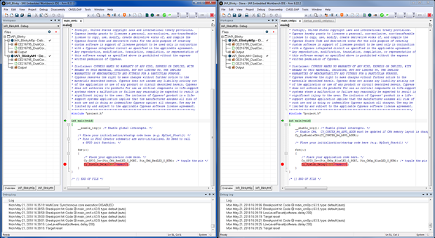
You can stop debugging in either window; debugging is ended for both CPUs. Press the kit reset button (RST/SW1) to restart kit operation
Connectivity application design considerations
ModusToolbox™ Connectivity, Wi-Fi, and Bluetooth® middleware libraries are made available through GitHub. These libraries can be used for developing wireless IoT applications using PSoC 6™ MCUs and Infineon’s AIROC™ Wi-Fi and Bluetooth® combo devices. The user has the option of choosing either the Arm® CM0+ or CM4 core for executing the connectivity application along with its necessary middleware and driver libraries. Throughput (data transmission speed in bits per second) and PSoC™ 6 MCU power consumption (in milliampere/microampere) are important factors to consider when deciding the core for the connectivity application. The related performance requirements play a crucial role in determining the optimal core to be used for the connectivity application. The following sections show the results of those analyses.
Throughput analysis
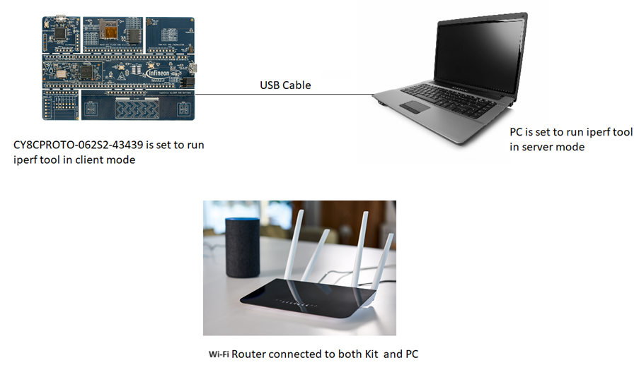
The below figure shows the test setup used for measuring the throughput. The CY8CPROTO-062S2-43439 kit is set up to run an iperf application in TCP client mode. The kit is connected to a PC running ModusToolbox™ via USB for programming and iperf log viewing. The KitProg3 USB-UART bridge is used with Tera Term software for log viewing. The PC also runs an iperf application in server mode. Both the kit and PC are connected to the same Wi-Fi router. The test setup is at a normal ambient setting meaning not inside a temperature/anechoic chamber.
The following table shows the achieved throughput with the default BSP settings with System Idle Power Mode set to Active, in a home Wi-Fi network:
| Scenario | Throughput (Megabits per second, Mbps) |
|---|---|
| CM0+ core sleep, CM4 core active @100 MHz | Peak = 21.9, Typical = 21.2 |
CM4 core sleep, CM0+ core active @100 MHz | Peak = 16.2, Typical = 15.9 |
Below are the screenshots of the iperf measurement output from both the kit and the PC.
CM4 execution:
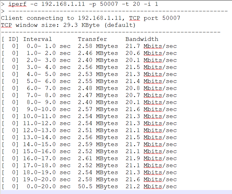
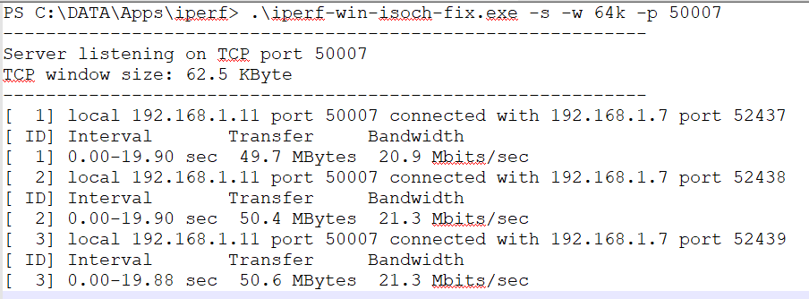
CM0+ execution
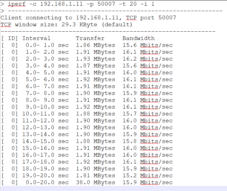
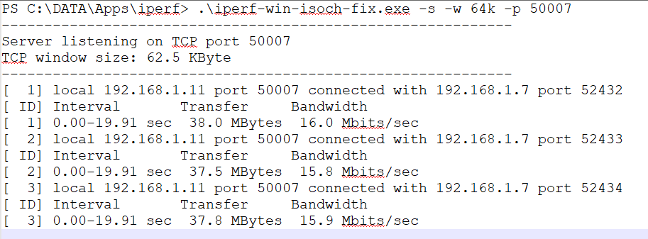
The above table and images clearly show that the CM4 core has approximately 5.7 Mbps higher throughput than the CM0+ core. So, we can conclude that running from CM4 generally results in higher throughput due to core architecture features compared to CM0+.
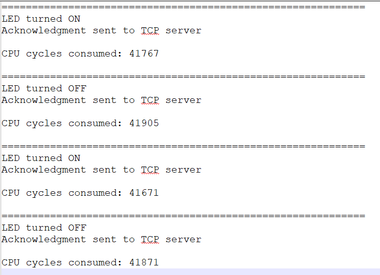
A TCP client application, which periodically receives data bytes, consumes approximately 42k CPU cycles per transfer on the CM4 core, as shown in the image above. The same can be saved by moving the Wi-Fi stack and application code to the CM0+ core, which can be utilized for other process intense tasks.
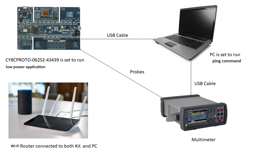
Power consumption analysis
The below figure shows the test setup used for measuring the power consumption. CY8CPROTO-062S2-43439 kit is set up to run the mtb-example-wifi-wlan-lowpower application in low-power mode is connected over USB cable to a PC running ModusToolbox™ for programming the kit. Both the kit and PC are connected to the same Wi-Fi router. On the kit, current measurement points are then connected to a multimeter to measure the current consumption.
The following table shows the achieved throughput with the default BSP settings, for 10 ping commands:
| Scenario | Current (mA) |
|---|---|
| CM0+ core sleep, CM4 core active @3.3 V | Peak = 3.42 mA, Average = 773 µA |
| CM4 core sleep, CM0+ core active @3.3 V | Peak = 2.58 mA, Average = 751 µA |
The figures below show the current measurement obtained from a power analyzer.
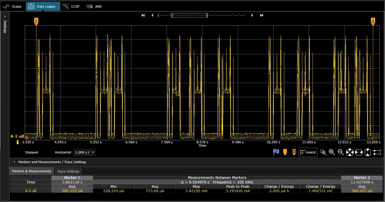
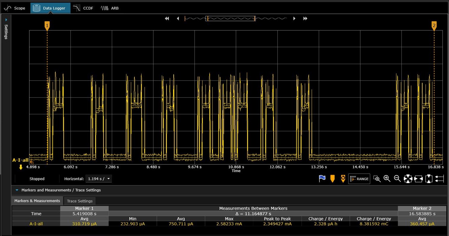
Table 2, Figure 47, and Figure 48 show that the peak current consumption is approximately 0.85 mA higher while running the application on the CM4 core compared to the CM0+ core. Please note that the application used in this example is designed to minimize power consumption by utilizing offload features such as packet filtering. As a result, there is only a slight difference in average current consumption between the cores. Therefore, we can conclude that running from CM4 generally results in higher current consumption due to core architecture features compared to CM0+.
Porting applications between cores
You can easily port ModusToolbox™ connectivity applications developed by you from one core to another (For example, from CM4 to CM0+) by following the guidelines in Infineon developer community article KBA236435.
This porting may be needed at times to evaluate the tradeoffs of requirements from the application.
Virtual Connectivity Manager
If you need to run connectivity applications on both the CM4 and CM0+ cores at the same time (For example, two MQTT clients), ModusToolbox™ offers a VCM library for sharing the connectivity libraries between the cores. This library uses the IPC mechanism to call connectivity-related APIs from a secondary connectivity core to a primary connectivity core. This way the application design becomes simple and save memory as there is no need to link the connectivity libraries on the binaries for both the cores. The mtb-example-wifi-dual-core-virtual-mqtt-client code example demonstrates the features of this library.
Summary
This application note has shown how to use and optimize your firmware and hardware designs for the dual-core feature in PSoC™ 6 MCUs.
Another way to optimize your PSoC™ 6 MCU design is based on the fact that PSoC™ devices are designed to be flexible and enable you to build custom functions in programmable analog and digital blocks. For example, PSoC™ 6 MCU has the following peripherals that can act as “co-processors”:
DMA controllers Note that the most common CPU assembler instructions output by C compilers are MOV, LDR, and STR, which implies that the CPU spends a lot of cycles just moving bytes around. Let the DMA controllers do that instead
Note: PSoC™ 6 MCU DMA controllers have an extensive set of features that enable you to construct complex data transfer and control systems that are independent of the CPUs. Software support of these features is provided in the ModusToolbox™ software Device Configurator, a PSoC™ Creator DMA Component, and an API in the PDL. For more information, see the Device Configurator Help Guide, the DMA Component datasheet, or the PDL documentation.
- Crypto block This block offers hardware acceleration for symmetric and asymmetric cryptographic methods (AES, 3DES, RSA, and ECC) and hash functions (SHA-512, SHA-256). It also has a true random number generator (TRNG) function. Software support for these features is provided by an API in the PDL; see the PDL documentation. The Infineon HAL does not have a crypto driver at the moment
- Universal Digital Blocks (UDBs) There are as many as 12 UDBs, and each UDB has an 8-bit datapath that can add, subtract, and do bitwise operations, shifts, and cyclic redundancy check (CRC). Datapaths can be chained for word-wide calculations. Consider offloading CPU calculations to the datapaths. At the moment, only PSoC™ Creator supports UDBs. ModusToolbox™ software does not have any support for UDBs
- UDBs also have programmable logic devices (PLDs) which can be used to
build state machines; see for example the Lookup Table (LUT) Component datasheet. LUTs
can be an effective hardware-based alternative to programming state machines in the CPU,
for example by using C switch/case statements.
In addition, two GPIO ports include Smart I/O™, which can be used to perform Boolean operations directly on signals going to, and coming from, GPIO pins. The Infineon HAL does not have support for Smart I/O
- Other smart peripherals include serial communication blocks (SCB), counter/timer/PWM blocks (TCPWM), Bluetooth® Low Energy, I2S/PDM audio, programmable analog, and CAPSENSE™. Use these peripherals to further offload processing from the CPUs
PSoC™ Creator and ModusToolbox™ software offer many Components and extensive APIs in the PDL to support the peripherals’ functions. This allows you to develop an effective multiprocessing system in a single chip, offloading many functionalities from the CPUs. This, in turn, can not only reduce code size, but by reducing the number of tasks that the CPUs must perform, presents an opportunity to reduce CPU speed and power consumption.
For example, you can implement a digital system to control multiplexed ADC inputs, and interface with DMA to save the data in the SRAM to create an advanced analog data collection system with zero usage of the CPUs.
ModusToolbox™ software provides a set of tools for setting up peripherals, pre-defined BSPs for all Infineon kits, libraries for popular functionality like CAPSENSE™ and emWin, and a comprehensive array of example applications to get you started.
Infineon offers extensive application note and code example support for PSoC™ peripherals, as well as detailed data in the device datasheets, PDL documentation, HAL documentation, and technical reference manuals (TRMs). For more information, see Related Documents.
References
For a comprehensive list of PSoC™ 6 MCU resources, see KBA223067 in the Infineon Support.
| Application notes | |
| AN228571 - Getting started with PSoC™ 6 MCU on ModusToolbox™ software | Describes PSoC™ 6 MCU devices and how to build your first ModusToolbox™ project |
AN221774 – Getting started with PSoC™ 6 MCU on PSoC™ Creator | Describes PSoC™ 6 MCU devices and how to build your first ModusToolbox™ or PSoC™ Creator project |
AN210781 – Getting started with PSoC™ 6 MCU with Bluetooth® low energy connectivity on PSoC™ Creator | Describes PSoC™ 6 MCU with Bluetooth® LE Connectivity devices and how to build your first PSoC™ Creator project |
AN217666 – PSoC™ 6 MCU interrupts | Describes PSoC™ 6 MCU interrupt architecture and how to configure interrupts |
AN219434 – Importing PSoC™ Creator Code into an IDE for a PSoC™ 6 MCU Project | Describes how to import the code generated by PSoC™ Creator into your preferred IDE |
| Code examples (PSoC™ Creator) | |
CE216795 – PSoC™ 6 MCU dual-CPU basics | Demonstrates the two CPU cores in PSoC™ 6 MCU doing separate independent tasks and communicating with each other using shared memory and the inter-processor communication (IPC) block |
CE223820 – PSoC™ 6 MCU IPC pipes | This example demonstrates how to use the inter-processor communication (IPC) driver to implement a message pipe in PSoC™ 6 MCU. The pipe is used to send messages between CPUs |
CE223549 – PSoC™ 6 MCU IPC semaphore | This example demonstrates how to use the inter processor communication (IPC) driver to implement a semaphore in PSoC™ 6 MCU. The semaphore is used as a lock to control access to a resource shared by the CPUs |
CE226306 – PSoC™ 6 MCU power measurements | This example shows how to achieve the power measurements listed in the PSoC™ 6 MCU datasheets |
| Code examples (ModusToolbox™) | |
This is a minimal starter Dual-CPU application template for PSoC™ 6 MCU devices | |
This example demonstrates how to use the inter-processor communication (IPC) driver to implement a semaphore in PSoC™ 6 MCU. The semaphore is used to lock to control access to a resource shared by the CPUs and synchronize the initialization instructions | |
This example demonstrates how to use the inter-processor communication (IPC) driver to implement a message pipe in PSoC™ 6 MCU. The pipe is used to send messages between CPUs | |
| PSoC™ Creator component datasheets | |
Supports generating interrupts from hardware signals | |
| Device documentation | |
| Development kit documentation | |
PSoC™ 6 Bluetooth® LE Pioneer Kit | |
PSoC™ 6 Wi-Fi Bluetooth® Pioneer Kit | |
PSoC™ 62S2 Wi-Fi Bluetooth® Pioneer Kit | |
PSoC™ 6 Bluetooth® LE Prototyping Kit | |
PSoC™ 6 Wi-Fi Bluetooth® Prototyping Kit | |
PSoC™ 62S3 Wi-Fi Bluetooth® Prototyping Kit | |
PSoC™ 62S1 Wi-Fi Bluetooth® Pioneer Kit | |
PSoC™ 62S1 Wi-Fi Bluetooth® Pioneer Kit | |
PSoC™ 62S2 Wi-Fi Bluetooth® Prototyping Kit | |
| Tool documentation | |
ModusToolbox™ software simplifies development for IoT designers. It delivers easy-to-use tools and a familiar microcontroller (MCU) integrated development environment (IDE) for Windows, macOS, and Linux | |
PSoC™ Creator enables concurrent hardware and firmware editing, compiling and debugging of PSoC™ devices. Applications are created using schematic capture and over 150 pre-verified, production-ready peripheral Components. Look in the downloads tab for Quick Start and user guides | |
| Installed by PSoC™ Creator 4.3 and available through GitHub. Visit mtb-pdl-cat1; for PSoC™ Creator, look in <PDL install folder>/doc for the User Guide and API Reference | |
Hardware Abstraction Layer (HAL) | Available through GitHub only. Visit mtb-hal-cat1 |
Revision history
| Document version | Date of release | Description of changes |
|---|---|---|
** | 2017-02-16 | New Application Note |
*A | 2017-03-08 | Updated Template |
*B | 2017-06-09 | Updated text and screen shots for release versions of PSoC™ Creator 4.1 and PDL 3.0.0 Other miscellaneous edits |
*C | 2017-08-23 | Minor edits Ported to new application note document template Confidential tag removed |
*D | 2018-03-07 | Added a new Figure 2 Updated Figure 4 and associated kit device part number Updated Figures 6 and 9 for PSoC™ Creator 4.2 beta 2 Emphasized using CM0+ as a support CPU for tasks such as Bluetooth® LE and CAPSENSE™ Added references to AN221111, Creating a Secure System; AN217666, PSoC™ 6 Interrupts; AN219528, PSoC™ 6 Low Power Modes; and CE216795, PSoC™ 6 Dual-CPU Updated power modes description Miscellaneous minor edits Ported to new application note template Changed the document title to PSoC™ 6 MCU Dual-CPU System Design |
*E | 2018-06-11 | Expanded section 4.3 to include dual-CPU debugging with µVision and IAR Embedded Workbench IDEs Updated power mode descriptions in section 3 Miscellaneous minor edits Ported to *Y application note template |
*F | 2018-06-12 | Added support for ModusToolbox™ |
*G | 2020-05-25 | Updated instructions based on ModusToolbox™ 2.1 Added HAL support |
*H | 2020-08-26 | Updated instructions based on ModusToolbox™ 2.2 |
*I | 2022-09-19 | Migrated to Infineon template Updated instruction based on ModusToolbox™ 3.0 |
| *J | 2023-08-03 | Updated link references |
| *K | 2023-12-01 | Added the Connectivity application design considerations section
and its subsection Removed the Techniques to improve throughput section |
| *L | 2024-02-09 | Replaced CY8CPROTO-062-4343W with CY8CPROTO-062S2-43439 and added reference to CY8CPROTO-062S2-43439 in the Development kit documentation table. |
Trademarks
The Bluetooth® word mark and logos are registered trademarks owned by Bluetooth SIG, Inc., and any use of such marks by Infineon is under license.