AN228753 PSoC™ 6 MCU usage of Direct Memory Access (DMA)
About this document
Scope and purpose
This application note provides advanced guidance on DMA in PSoC™ 6 MCU and its use cases.
Introduction
A Direct Memory Access (DMA) block is specifically designed for data movement and is therefore more efficient than CPU for transferring large data blocks. In a system, DMA blocks also provide an independent data transfer engine, which relieves the CPU of bandwidth for data transfers. DMA blocks in PSoC™ 6 MCU implement a data transfer engine with different configurations and settings that let the DMA block be used in different data transfer use cases. This application note describes these different DMA configurations and use cases, and explains how to design with DMA to achieve the most efficient and fastest data transfers, and provides guidance for calculating the performance of a DMA transfer in the number of clock cycles.
DMA in PSoC™ 6 MCU is specifically designed to cater to data transfer requirements of a System on Chip (SoC). For this reason, there are two types of DMA engines in some of the PSoC™ 6 MCU devices.
DMA (DW) (also called Datawire): This DMA engine is specifically designed for transferring small data blocks, typically between peripherals, to offload the CPU from any data transfer with peripherals. In this document, this DMA engine will be referred to as DMA (DW) or DW.
DMAC (DMA Controller): This DMA engine is specifically designed to efficiently transfer large data blocks in memory. The DMAC provides higher performance compared to DMA/DW. In this document, this DMA engine is referred to as DMAC.
In addition to the two types of DMA hardware blocks, there are multiple other implementation-level features such as X and Y loops, different triggering schemes, and trigger routing. See the Technical Reference Manual (TRM).
This document will use the term DMA to generally refer to a feature or explanation for both DMA(DW) and DMAC.
Architecture
There are two types of DMA hardware blocks implemented in PSoC™ 6 MCU devices: DMA/DW and DMAC. Both DMA/DW and DMAC have similar feature sets and architecture, but differ in their performance and use cases; see Differences between DMA (DW) and DMAC. This section provides a general high-level description of the DMA block architecture. For a more detailed explanation of individual features, see the Technical Reference Manual (TRM).
The DMA transfer engine implements the state machine from the time a trigger is received, to when the transfer is completed. Figure 1 shows the block diagram of the DMA hardware block.
The DMA hardware block can implement multiple DMA channels that can be independently configured for different data transfers. At a time, only one DMA channel can be active in a DMA block; other channels, if triggered, are put in a pending state. When the DMA hardware block completes the current active channel, pending channels are evaluated based on their priorities.
The data transfer associated with a DMA channel is described by a descriptor. The descriptor defines different configurations of the transfer such as size, data width, burst sizes, address increment schemes, and source and destination addresses. The descriptor is a structure of a specific type placed in a memory location. The pointer to this descriptor is associated with a DMA channel as part of its DMA channel configuration. When a DMA channel is made active, the first action is to fetch its descriptor from the memory. The descriptor could be in any form of memory: RAM, flash, or even an external memory. Multiple descriptors can be associated with a DMA channel in a chained configuration: see Chaining descriptors.
The DMA hardware block connects to the system through two data bus interfaces and a set of trigger signals. The bus master interface is used for data transfers by the DMA block, while the bus slave interface is for other masters to access and configure DMA.
Each DMA channel has a trigger input, trigger output, and interrupt output line. Interrupt signals are routed to individual interrupt lines in the respective CPU. Trigger signals to and from DMA channels are routed through a trigger multiplexer block, which has a device-specific architecture. The trigger multiplexer block enables routing of trigger signals from different peripherals to the DMA block and routing trigger outputs back to other peripherals.
To understand specific trigger routes in a specific PSoC™ 6 MCU device, see the “Trigger Multiplexer Block” chapter in the Technical Reference Manual (TRM).
Figure 1. DMA architecture

Transfer modes
There are three transfer modes for a DMA channel as defined by its associated descriptor:
-
In a Single transfer, the DMA descriptor transfers only a single data element. A data element could be a byte, 2 bytes, or a 4-byte word based on the width definition in the descriptor. Each single transfer would need to be initiated by a trigger signal to the DMA channel
-
1D transfer (X loop) is useful for buffer-to-buffer transfer or a peripheral-to-memory buffer transfer; it allows for multiple data elements to be transferred as defined in a descriptor. The descriptor can decide on the exact form of source and destination address increments. You can choose to trigger the transfers one data element at a time or the entire 1D transfer at a time
-
The 2D transfer (Y loop) mode allows for multiple 1D transfers to be defined in a single descriptor. This allows for a larger data count and allows for transfers of more complex data entities like array of data structures. The trigger scheme allows for triggering individual data elements, an entire 1D transfer, or the entire 2D transfer at a time
DMA design
Setting up a DMA channel using ModusToolbox™ involves multiple steps described in the following sections. The instructions assume that you have a basic understanding of bringing up a project using ModusToolbox™. See AN228571 – Getting Started with PSoC™ 6 MCU on ModusToolbox™. The following sections take an example use case of an ADC triggering a DMA channel at the end of conversion. The DMA channel transfers the ADC result data to a memory buffer. The memory buffer is meant to be a 32-element-long array and therefore, the DMA descriptor will be configured to transfer the ADC result 32 times to fill the buffer array.
Steps for setting up a typical DMA channel are shown as numbered in Figure 2.
Step 1: Choose the DMA channel
DMA channel trigger connections to peripherals are dependent on the design of the Trigger Multiplexer block. The choice of the DMA channel to use will depend on the trigger routing from the peripheral that is triggering the DMA channel. In this case, because the source of the DMA trigger is an ADC, you will need to refer the trigger routing and find the DMA channel associated with the ADC trigger outputs. In the case of the PSoC™ 62 CY8C62x8 or CY8C62xA device, DMA channel 28 provides this routing connection to the ADC as shown in Figure 2. See the Technical Reference Manual (TRM) for a detailed discussion of Trigger Multiplexer block design.
After you identify the DMA channel, use the DMA tab in Device Configurator in ModusToolbox™, as shown in Figure 2. Enable the DMA channel that you are planning to use, and then configure its parameters on the right of the screen. You can configure one or more DMA descriptors, DMA channel parameters, and the trigger input and output routing.
Figure 2. DMA configuration
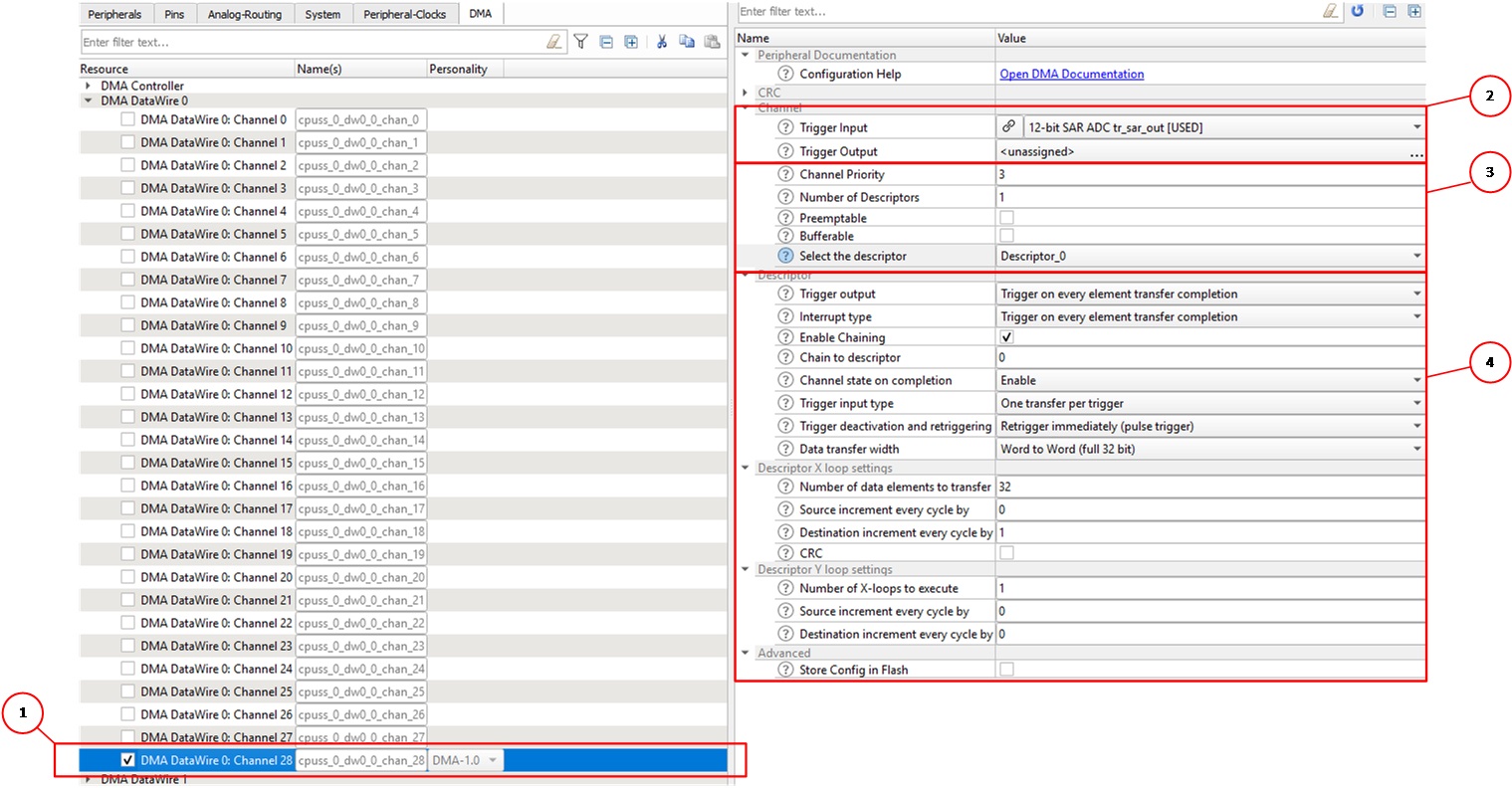
Step 2: Configure triggers
The trigger input and outputs of a DMA channel are determined by the requirements of the system you are building. For the example of an ADC triggering the transfer of data from its result register to a memory buffer, the trigger input needs to be set to connect to the ADC trigger signal. You can configure the peripheral that will trigger the DMA channel by selecting the “Trigger Input” setting in the DMA channel settings. You can also configure how to route the trigger output from the DMA. Both these settings automatically configure the trigger multiplexer block routing.
Step 3: Set up the DMA channel
The channel configuration involves setting up channel-level parameters such as channel priority, preemptable, and bufferable. Here, you set the number of descriptors to be configured, and specify the descriptor that needs to be associated with the DMA channel when the channel is initialized.
Step 4: Set up the DMA descriptor
Based on the number of descriptors configured, the Select Descriptor field will have an option to select and configure as many descriptors as set in the Number of Descriptors field. Select each descriptor and configure it.
In the descriptor configuration, you can configure the trigger and interrupt behavior. In the case of multiple descriptors that need to be chained, select Enable Chaining and then select the descriptor to chain to in the Chain to descriptor field. You can also configure the X and Y loop transfers. Select Store Config in Flash to store the descriptors in flash.
Step 5: Write the user code
After configuring the triggers, channel, and descriptors, save and close the configurator. This automatically generates the code in the cycfg_DMAs.h and cycfg_DMAs.c files. Each descriptor will generate a descriptor structure called cpuss_0_dw0_0_chan_28_Descriptor_0 in the code. Note that this descriptor is not automatically initialized or allocated to the DMA channel. This must be done in user code.
-
A configuration structure named cpuss_0_dw0_0_chan_28_Descriptor_0_config is generated, which has all descriptor configuration set in the Device Configurator. This can be used to initialize the descriptor cpuss_0_dw0_0_chan_28_Descriptor_0
-
All channel-level configuration such as priority is configured in cpuss_0_dw0_0_chan_0_channelConfig. This structure can be used to initialize the channel
In addition, you need the following user code to initialize and enable DMA transfers:
- Initialize the descriptor with the following function. This step transfers all configuration to the descriptor
- Configure the source and destination addresses with the following functions:
- Initialize the channel and associate the descriptor to it with the following function:
- Enable the channel using the following function:
- Note that at this stage, only the channel is enabled but not the DMA block itself. To enable the DMA block, use the following function:
Cy_DMA_Descriptor_Init(&cpuss_0_dw0_0_chan_0_Descriptor_0, &cpuss_0_dw0_0_chan_0_Descriptor_0_config);
Cy_DMA_Descriptor_SetSrcAddress(cpuss_0_dw0_0_chan_0_Descriptor_0, SAR->CHAN_RESULT);
Cy_DMA_Descriptor_SetDstAddress(cpuss_0_dw0_0_chan_0_Descriptor_0, &Buffer);
Cy_DMA_Channel_Init(cpuss_0_dw0_0_chan_0_HW, cpuss_0_dw0_0_chan_0_CHANNEL, &cpuss_0_dw0_0_chan_0_channelConfig);
The initialization also automatically associates cpuss_0_dw0_0_chan_0_Descriptor_0 to the channel.
Cy_DMA_Channel_Enable(cpuss_0_dw0_0_chan_0_HW, cpuss_0_dw0_0_chan_0_CHANNEL)
Cy_DMA_Enable(cpuss_0_dw0_0_chan_0_HW);
Priorities and preemption
A single DMA hardware block can support many DMA channels which may be triggered by independent and unrelated events. This leads to the possibility of multiple DMA channels going to a pending state at the same time and contesting for bus access.
Every DMA channel has an associated priority value, which is used by the DMA hardware block’s priority decoder to choose the channel when multiple channels are pending in the same DMA block. In such a situation, the DMA channel with the lowest priority number gets active and others are held pending. There are only four priority levels (0-3), while there can be more than four DMA channels present. In such cases, where multiple DMA channels of the same priority level are contesting for the bus, a round robin scheme of arbitration is employed.
However, if there is a low-priority channel already active and is in the middle of a large transfer, a pending higher-priority channel cannot become active. This can hold the execution of a higher-priority channel. This can be a problem when the higher-priority channel caters to a data transfer that is time-sensitive. Figure 3 shows this condition in the case of Channel Without Preemption.
To address this, there is an additional configuration parameter in the DMA channel called “Preemptable”. This parameter allows a higher-priority channel to preempt the currently active low-priority channel. If a channel has Preemptable enabled, any other channel with a higher priority can preempt the channel. This means that even when the DMA channel is in the middle of a transfer, a higher-priority channel request will stop the current transfer after completing the current atomic transfer, keep the channel pending, and then start the higher-priority channel. The Data Width parameter determines the size of an atomic transfer. Only when the high-priority channel is completed, the low-priority channel may resume. A low-priority preemptable channel can get preempted multiple times during a single transfer. See Figure 3.
Preemption is useful only in cases when there are low-priority channels with no constraints of transfer times and there are high-priority channels that are time-sensitive and cannot be held hostage by other on-going transactions.
Note that preemption can cause significant delay in low-priority transfers, if:
-
There are multiple frequent requests from high-priority channels
-
The time taken for a high-priority transfer is too long
Figure 3. Channel arbitration and preemption in DMA

Data transfer widths
The data width determines the width of the data being accessed at the source or destination. This setting is also responsible for the value of each increment of the X or Y loops. Data widths must always be equal to the width supported by the device. For example, because all peripherals support 32-bit data width, if the source or destination of a transfer is a peripheral, the source or destination data width must be set to 32 bits.
Memory supports 8-bit, 16-bit, and 32-bit access. You can use larger data widths to increase throughputs, or use smaller data widths to quantize the data size. For example, 8-bit data is being transferred from a communication block to the memory, the source data width must be 32 bits (because the source is a peripheral), but the destination can be 8 bits (because the destination is a memory location), which automatically truncates the higher 24 bits. This will enable a smaller memory footprint.
Types of transfers
1-to-1 transfer
This form of transfer allows for one data element to be transferred from a source to a destination. A good example is the peripheral-to-peripheral transfer shown in Figure 4. This shows an SPI block and a UART block. The data coming on SPI Rx is directly transferred to UART Tx using DMA channel 0; similarly, the data coming on UART Rx is directly transferred to SPI Tx. The implementation utilizes the Rx interrupt of both the communication blocks to trigger DMA channels.
Figure 4. 1-to-1 transfer

Figure 5 shows the configuration for a 1-to-1 transfer. When the X and Y loops are configured to execute only once, the configurator automatically configures the DMA channel for a single transfer. This form of transfer is useful when a specific data transfer path is set up with a trigger, and is expected to work without CPU intervention.
Figure 5. Setting up a 1-to-1 transfer
1-to-N transfer
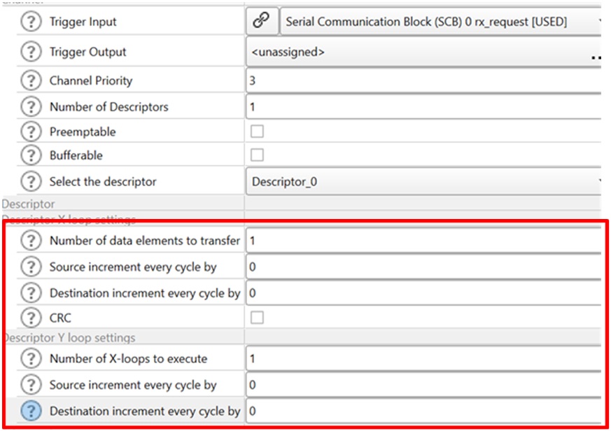
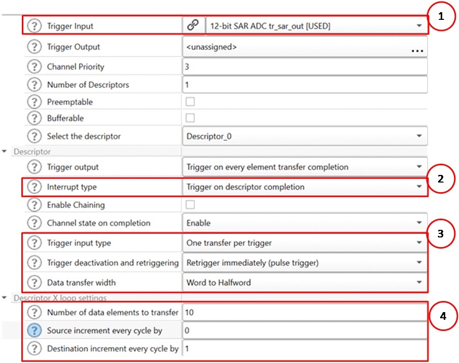
Transfer from a single source address to multiple destination addresses is a typical use case for transfers from peripherals like ADC to memory buffers for further processing by the CPU. The example in Figure 6 shows an ADC output being DMA-transferred to a memory buffer. The ADC has a 12-bit resolution; therefore, the result is in a 16-bit data register, and the buffer is a 16-bit array. At the end of the entire buffer transfer, the DMA creates an interrupt for the CPU, so it can start post-processing on the buffered data.
The configuration for this example is shown in Figure 7.
-
The trigger source is set to the SAR ADC, so the ADC trigger is automatically routed to the DMA channel
-
The interrupt is configured to trigger when the transfer is completed. This will enable the CPU to act on the buffer once the entire buffer is filled
-
The trigger input is configured to have one transfer in each ADC trigger. The data transfer width is configured to “Word to Halfword”. The ADC is a peripheral and therefore, the peripheral interface is 32-bit. The destination is a 16-bit buffer in memory
-
The X loop is set to run 10 times (which is the size of the buffer), while only the destination is incremented for each element transferred. The source remains constant because it is always the ADC result register
Figure 6. ADC to buffer: 1-to-N transfer configuration for ADC to buffer

Figure 7. Configuration for ADC to buffer
Noncontiguous source/destination increments
In this transfer mode, you can also have the output placed in noncontiguous locations of the memory. This is useful if the destination was an array of structures and you are only filling a specific element in that array. An example is the destination that has an array of structures with each structure element comprising a 32-bit time stamp followed by a corresponding ADC result reading. This implementation is shown in Figure 8. If a DMA channel was transferring only time stamp data, it would need to interleave destination addresses. This is accomplished by having a destination increment value greater than 1. The following use case independently transfers the time stamp data from its timer source, and the ADC result from the ADC.
Figure 8. Example of transferring to noncontiguous destination addresses
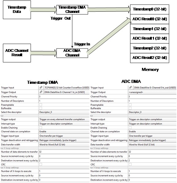
The transfer can be accomplished by using two DMA channels with the time stamp channel triggering the ADC channel. In this case, the X loop settings will use a destination increment of 2. This will accomplish placing every result in the right interleaved location in the array. The same setting is used for both DMA channels.
N-to-1 transfer
This uses only an X loop transfer, but the source increments while the destination is constant, for example, when there is a waveform data stream in memory and it needs to be streamed to a DAC over SPI. Such an implementation will simply have non-zero increment for the source and a zero-increment value for the destination. The source can also be incremented by numbers greater than 1 for cases like the ones discussed in 1-to-N transfer.
N-to-N transfer
This is a use case for X loop when both source and destination addresses are incrementing such as a memory-to-memory transfer between flash and RAM for copying the configuration data to register blocks, or copying of a block of memory from the external to the internal memory.
Figure 9. N-to-N transferN-to-N with dissimilar increment

Typically, such large data transfers between memories are time-critical. In such cases, you should use DMAC for better transfer speed.
Variations in this model are possible by using dissimilar source and destination increment values, such as shown in Figure 10. Here, there is already mixed-in left and right channel audio data in the source memory location.. They need to be separated into different buffers for audio processing. In this case, you can use two descriptors in a single channel. The first descriptor will transfer the left channel to its destination register while the second descriptor will transfer the right channel. However, each DMA descriptor will have source increments of 2 and destination increments of 1.
Figure 10. N-to-N with dissimilar increment

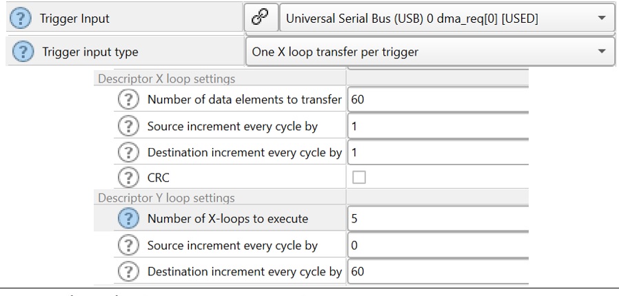
N-to-NxM
N-to-NxM is a case for using X and Y loops such as a structure that is getting transferred to an array of structures. Assume that there is a data structure coming over as a USB packet in every frame. This 60-byte long structure needs to be buffered into an array in the memory for further processing later as shown in Figure 11.
The configuration of X and Y loops for this transfer is shown in Figure 12. Note that the source and destination are incremented in the X loop. This is the phase when the structure is being moved. Each X loop is used to move individual instances of the structure from USB to the buffer. After each X loop, the source address is reset back to the start of the source USB address because the Y source increment is zero. However, the Y loop destination increment is 60 (the size of the structure); this makes the next instance of the structure to get written as the next array element in the destination.
The scenario shown in Figure 10 can also be implemented by using a N-to-NxM transfer with two X loops. The first time the X loop runs, it will transfer Audio L data from the source to the destination; the second time, it will transfer the Audio R data. The X loop increments will be two bytes on the source and one byte on the destination. However, the Y loop source increment will be 1. This is to ensure that after the first X loop, the next X loop starts at a ‘1’ offset to get the R channel. The Y destination increment will be the distance between the Audio L and Audio R addresses.
Figure 11. N-to-NxM transferConfiguration for an N-to-NxM transfer

Figure 12. Configuration for an N-to-NxM transfer
Chaining descriptors
DMA blocks support descriptor chaining, which is useful if different types of transfers are to be done in a sequence. Each descriptor has the pointer to the next descriptor it must chain to, similar to a linked list. There is no limit on the number of descriptors you can chain. One of the greatest advantages of chaining is that each descriptor can have a different configuration including different source/destination addresses, trigger settings, interrupt settings, transfer modes, loops settings, and data widths. This allows the same DMA channel to implement multiple transfers of varying characteristics.
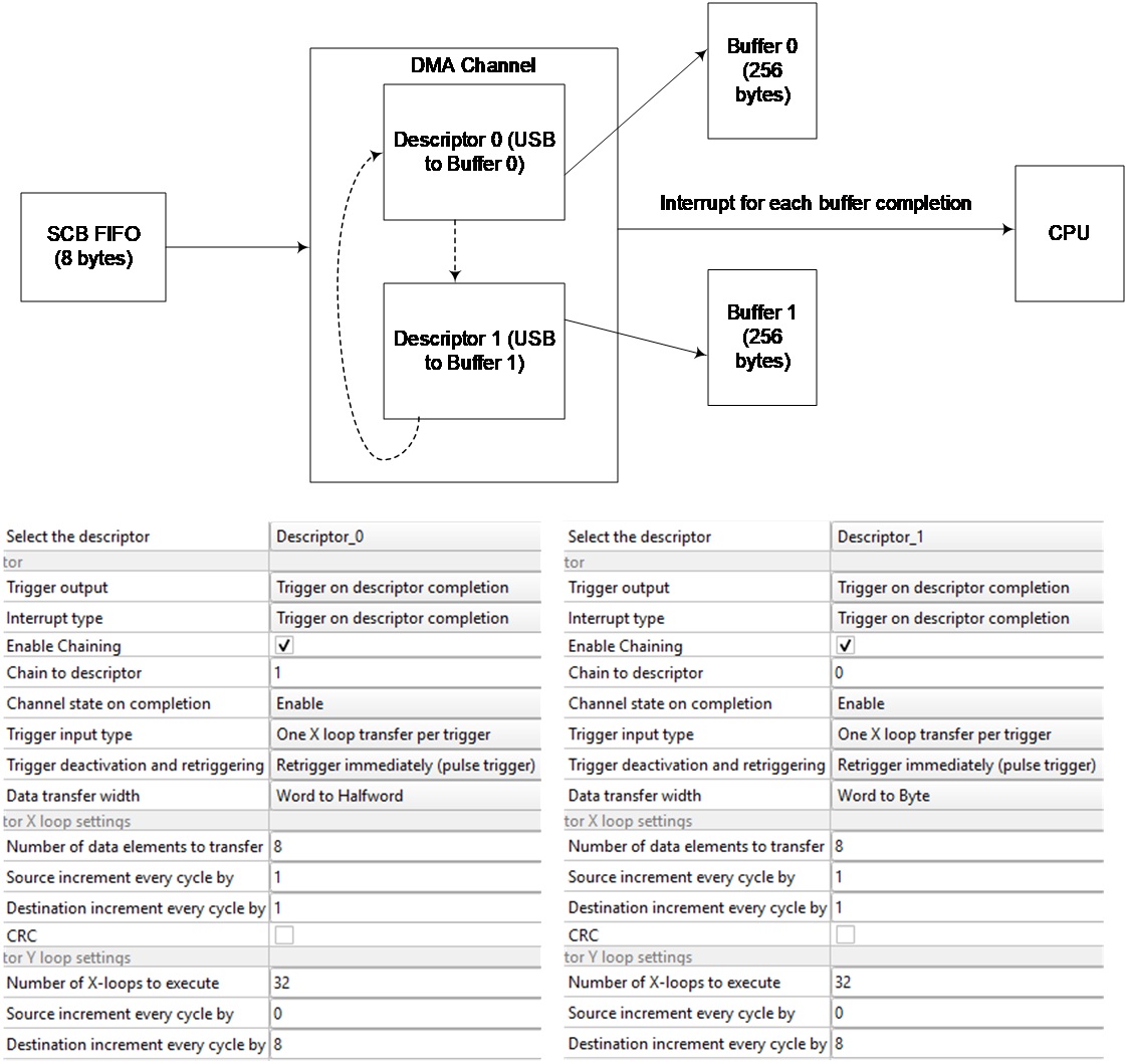
A good use case for descriptor chaining is double buffering as shown in Figure 13. The input data comes in the form of 8-byte blocks in the SCB FIFO, which needs to be moved to Buffer 0 or 1 for double buffering. The buffers are 256 bytes each and therefore can accommodate 32 FIFOs worth of data before overflowing. A single DMA channel is used for the transfer, with two descriptors. Both descriptors are set up for a 2D transfer with the FIFO as the source. The X loop will cycle through the FIFO and therefore needs both source and destination increments. The Y loop handles the moving of 32 FIFOs. Descriptor 0 is set to chain to Descriptor 1 and vice versa. Descriptor 0 is configured to transfer to Buffer 0 and Descriptor 1 to Buffer 1.
Once Descriptor 0 is completed, the control automatically transfers to Descriptor 1 due to chaining. This will ensure continued transfer and double buffering. Each descriptor is also configured to interrupt the CPU at its transfer completion. This will inform the CPU that one buffer is available for processing.
Figure 13. Double-buffering using descriptor chaining
Chaining DMA channels
In addition to chaining of descriptors in a single DMA channel, there are cases where it is useful to chain two DMA channels. To do this, one DMA channel’s trigger output is routed to the next DMA channel’s trigger input. Depending on the specific trigger multiplexer routing in a given PSoC™ 6 MCU device, only certain DMA channels will have the ability to chain. See the “Trigger Multiplexer” chapter in the Technical Reference Manual to understand the chaining restrictions of DMA channels.
A good example where DMA channels are chained is shown in Figure 14. Here, the ADC input is a large analog mux. Because the number of input channels is large, it is not supported by the inbuilt multiplexer in the ADC hardware. This analog multiplexer must be implemented using an Analog Mux resource that must have routing registers modified to connect each channel. When an ADC conversion is completed, the ADC DMA channel is triggered. This moves data from the ADC result register to the memory buffer. After completion of the transfer, the ADC DMA channel triggers the MUX DMA channel. The source for this channel is a set of memory locations with preset routing values for the routing registers. Whenever this DMA channel is triggered, it transfers the new routing values to the Analog Mux registers, which effectively switch the channel.
Figure 14. DMA channel chaining example

Differences between DMA (DW) and DMAC
The main difference between DMA (DW) and DMAC relates to their usage. DMA (DW) is meant as a small data size, transactional DMA transfer. It would typically be used for transferring bytes between peripherals like from ADC to RAM. Using DMA (DW) for large transaction is expensive on a system due to its relatively low performance.
DMAC is substantially more efficient than DMA (DW) in transferring large blocks of data and should be used whenever there is a need to transfer large amounts of data in memory. DMAC focuses on achieving high memory bandwidth for a small number of channels.
There are some architectural differences in DMAC that facilitate a higher performance.
DMAC has a dedicated channel logic with dedicated channel state register for each channel. This helps retain the channel state through arbitration or preemption. Therefore, DMAC will incur fewer cycles while arbitrating between channels. This is particularly beneficial when working with multiple channels transferring large blocks of data.
DMAC has a special transfer mode called the “memory transfer mode”, which is specifically designed for fast memory-to-memory transfers. The mode is a specialized 1D transfer, where the source and destination increments are fixed to 1.
DMAC also has a 12-byte FIFO which is used for prefetch. The prefetch works by prefetching the source data as soon as the channel is enabled. When the channel is triggered, the prefetched data is simply transmitted to the destination. This shortens the initial delay of data transmission. However, this feature should be used with care to ensure that data synchronization is not violated. If the source data changes between transfers, using the prefetch buffer is not recommended because it can lead to data synchronization issues.
DMA transfer performance
The DMA block runs on the slow clock of PSoC™ 6 MCU. This section will analyze and detail how to determine the performance of a DMA transfer based on its settings. All data is based on slow clock cycles. The performance calculation numbers for all interactions over the bus presume that there is no delay due to bus arbitration. If there is such a delay, that should be added to the calculation.
Elements of a transfer
A transfer can be split into multiple operations as shown in Table 1 with the corresponding cycles needed for their execution. Each transaction is initiated by a trigger, which goes through trigger synchronization circuit and takes up two cycles. These two cycles will be consumed whenever there is a trigger event being used. Loading the channel configuration takes three cycles. The loading of descriptors and the next pointer is done over the bus and therefore depends on the arbitration on the bus. Similarly, data transfers are also over the bus and therefore dependent on the arbitration happening on the bus. After the descriptor and next pointer are loaded, the DMA engine starts data transfer from the source address to the destination address. The data transfer consumes three cycles per data element.
Operation | Cycles (Slow Clock Cycles) |
|---|---|
Trigger Synchronization and Priority decoding | 3 |
Start state machine and load channel config | 3 |
Load descriptors | 4 for single transfer 5 for 1D transfer 6 for 2D transfer |
Load next pointer | 1 |
Moving data from source to destination | 3 |
A simple single transfer will take 14 cycles. However, with the next trigger, it still must go through all 14 cycles to set up the transfer. Therefore, single transfers are not very efficient for moving multiple elements of data.
Figure 15. Timing diagram for a single transfer on the DMATiming diagram for N-byte transfer in 1D and 2D modes

1D and 2D transfers are more efficient in this regard even though they incur extra cycles to fetch additional words in the descriptor. However, these are incurred only on the first transaction; every subsequent transaction will only consume three cycles. This is shown in Figure 16. Note an additional cycle is required to fetch the descriptor in a 2D transfer, but 2D transfer supports more transfer sizes compared to 1D transfer. Therefore, for larger data transfers, 2D transfer is more efficient.
Figure 16. Timing diagram for N-byte transfer in 1D and 2D modes

To understand this better, compare the three transfer modes (Table 2) if transferring 1024 words of data. Single transfer is configured to run 1024 times. 1D transfer has a limit of 256 words per X loop. So, it would run the descriptor four times. 2D transfer will have an X loop of 256 words and a Y loop of 4 X loops.
2D transfers can move the largest amount of data at the highest throughput on a single trigger, while single transfers are the least efficient, because they treat every transaction as a new transfer and go through all the cycles of setting up the channel. Therefore, single transfers are only useful in making single element transfers on a trigger. Using single transfers to implement bulk transfers is not recommended.
| (Number of cycles) | Single transfer (one transfer per trigger) | 1D transfer (entire descriptor per trigger) | 2D transfer(entire descriptor per trigger) |
|---|---|---|---|
First element transferred (1 time) in number of slow clock cycles | 14 | 15 | 16 |
First element of each X loop (3 times) in number of slow clock cycles | 14 | 15 | 3 |
All other transfers in number of slow clock cycles (1020 times) | 14 | 3 | 3 |
Total (1024 bytes) in number of slow clock cycles | 14336 | 3120 | 3085 |
Throughput (MB/s) Slow clock= 50 MHz Transfer width= 32-bit | 14.28 | 65.64 | 66.68 |
DMA (DW) and DMAC: trigger schemes and performance
Note that whenever a trigger is to be processed, the DMA (DW) incurs the entire 14-16 cycles (depending on the transfer mode). This is because every time the DMA hardware block is in a state where it needs to wait for a trigger, it may switch channels to service other pending channels. So, when the next trigger is initiated, DMA (DW) goes through the additional cycles needed to start the transfer. Thus, performance is degraded where triggers are processed more often. Table 3 compares trigger schemes in a 2D transfer for a DMA (DW) that is set up to transfer 1024 bytes.
| (Number of cycles) | 2D transfer(one transfer per trigger) | 2D transfer(one X loop per trigger) | 2D transfer(entire descriptor per trigger) |
|---|---|---|---|
First element transferred | 16 | 16 | 16 |
First element of each X loop | 16 | 16 | 3 |
All other transfers | 16 | 3 | 3 |
Total (slow clock cycles) (1024 bytes) | 16384 | 3124 | 3085 |
On DMAC, the DMA transfer engine logic is replicated per channel with channel-level memory to hold the state while switching channels. For every trigger, the DMAC does not have to fetch all channel and descriptor information. The only extra cycles incurred are for trigger sync and priority decoding. This means that DMAC will perform better in a transfer that is triggered multiple times. Figure 17 shows this comparison of performance between DMAC and DMA (DW) using a timing diagram.
Figure 17. Performance comparison of DW and DMAC for a triggered mode of transfer

Also note that, when a transaction is waiting for a trigger, it could get preempted by another channel. This can lead to additional delays waiting for the preempting channel to relieve the DMA hardware block. This is especially an issue when dealing with a system with multiple DMA channels which have competing priorities.
From this performance comparison it is clear that
-
Transfers are more efficient when transactions are done in bulk without waiting for triggers. Triggering requirement adds delay
-
Using 2D transfers improves performance when the entire transfer is completed in a single trigger
-
Waiting for a trigger can seriously drop performance due to the possibility of arbitration with other channels in the DMA hardware block
-
If there is a need to use a trigger for individual transfer elements, using the DMAC will give you a better performance than the DMA (DW)
Preemption and its impact on performance
The choice of making a DMA (DW) channel as preemptable affects its performance. This is because every time a channel is preempted, the following happen:
-
The channel is in pending state for as long as a higher-priority channel is running
-
On resumption, the channel descriptor must be fetched again, costing additional cycles for every resume. So, if there are large number of higher-priority channels, making a low-priority channel preemptible can have adverse effects on its throughput
During preemption, the throughput of a low-priority DMA (DW) channel is affected by the delay caused by the high-priority channel and the extra cycles incurred for each time it was preempted. If the low-priority channel was transferring large blocks of data, this can incur multiple instances of preemption and the effect of the extra cycles incurred start hurting the throughput.
This impact is limited for DMAC channels because they do not need to go through the entire descriptor fetch cycle when resuming after a preemption. This means that the throughput of a low-priority DMAC channel is only affected by the delay caused by the high-priority channel. When transferring large blocks of data through a low-priority preemptable channel, it is better to use DMAC for a better throughput.
The performance comparison in a preemption scenario is shown in Figure 18.
Figure 18. Comparing performance of DMAC and DMA(DW) in a preemption scenario

On the other hand, if there is a low-priority channel that is transferring a large amount of data, not making it preemptable can starve other high-priority channels for too long. Only channels whose data transfers are not time-critical can be made preemptable.
Sometimes, you can also distribute channels across multiple DW blocks to avoid conditions of preemption and deal with contention at the bus arbitration level.
Bus arbitration and its impact
There are multiple bus masters in the PSoC™ 6 MCU device. A DMA channel may have the highest priority in its DMA hardware block, but that does not guarantee its performance on the bus when arbitrating with other bus masters. Sometimes, even a DMA channel’s descriptor fetch process can be delayed due to bus arbitration by other masters. This issue can be minimized by controlling the arbitration scheme configured in PROT_SMPU_MSx_CTL[PRIO]. For more details, see the Registers TRM.
Summary
PSoC™ 6 MCU family devices offer two types of DMA blocks: DMA (DW) and DMAC. The DMA (DW) offers a lot of DMA channels meant for small data size transfers, typically between peripherals and memory. The DMAC is a high-performance DMA meant for large data transfers, typically between memory locations, with maximum throughput.
References
For a comprehensive list of PSoC™ 3, PSoC™ 4, and PSoC™ 5LP resources, see KBA86521 in the Infineon community.
Application Notes
AN210781 – Getting Started with PSoC™ 6 MCU with Bluetooth® Low Energy Connectivity: Describes PSoC™ 6 MCU with Bluetooth® LE Connectivity devices and how to build your first PSoC™ Creator project
AN215656 – PSoC™ 6 MCU: Dual-CPU System Design: Describes the dual-CPU architecture in PSoC™ 6 MCU, and shows how to build a simple dual-CPU design
AN219434 – Importing PSoC™ Creator Code into an IDE for a PSoC™ 6 MCU Project: Describes how to import the code generated by PSoC™ Creator into your preferred IDE
Code Examples
CE218553 – PWM Triggering a DMA Channel
CE218552 – UART to Memory Buffer Using DMA
CE225786 – PSoC™ 6 MCU USB Audio Recorder
CE222221 – PSoC 6 MCU Voice Recorder
CE220762 – PSoC 6 MCU PDM to I2S Example
Device Documentation
PSoC 6 MCU: PSoC 63 with BLE Datasheet
PSoC 6 MCU: PSoC 63 with BLE Architecture Technical Reference Manual
Development Kit Documentation
CY8CKIT -062- BLE PSoC 6 BLE Pioneer Kit
Tool Documentation
PSoC™ Creator: Look in the Downloads tab for Quick Start and User Guides
Peripheral Driver Library (PDL): Installed by PSoC™ Creator 4.2. Look in the <PDL install folder>/doc for the User Guide and the API Reference
ModusToolbox™ Software: Look in the Quick Panel under the heading Documentation. Alternately look in the install directory for ModusToolbox™ <ModusToolbox install folder>/doc WICED SDK with PSoC™ 6 Support: Installed with ModusToolbox™ Software
Revision history
Document version | Date of release | Description of changes |
|---|---|---|
** | 2020-05-29 | Initial release |
*A | 2021-02-23 | Updated in Infineon template |
*B | 2022-07-21 | Template update |
*C | 2023-08-17 | Updated link references |