AN228740 Usage of Quad SPI (QSPI)/Serial Memory Interface (SMIF) in PSoC™ 6 MCU
About this document
Scope and purpose
AN228740 provides the guidelines for using QSPI/SMIF in PSoC™ 6 MCU. The PSoC™ 6 MCU QSPI delivers an interface for communicating with external serial memory devices. This application note explains how to incorporate QSPI into an application in either eXecute In Place (XIP) mode or Command mode. This application note describes the features available in the block and how to configure those features for your application.
Associated part family
More code examples? We heard you.
To access an ever-growing list of hundreds of PSoC™ code examples, please visit our code examples web page. You can also explore the video training library here.
Introduction
An MCU is used to process data from sensors or other external devices in many embedded systems. The MCU often has limited on-chip memory for data storage beyond the processing firmware that the MCU is executing. This can make processing more significant data types, such as images and audio files, complex as the file cannot fit in the MCU’s memory. Additionally, as algorithms become more complex and firmware images grow in size, an MCU’s on-chip memory may not be large enough. To remedy this lack of memory, external serial memory devices can be added to an embedded system to greatly increase available storage.
The PSoC™ 6 MCU includes a serial memory interface (SMIF) hardware block that simplifies access to external serial memory devices. This block supports a variety of SPI-based serial interfaces, including standard SPI, Dual-SPI, Quad-SPI, Dual Quad-SPI, and Octal SPI. The block also supports eXecute-In-Place (XIP) mode operation, so that large firmware images can be executed directly from the external memory with minimal latency.
This application note shows you how to use QSPI to communicate with serial memory devices with the Infineon PSoC™ 6 MCU device. The document opens with two simple software approaches to using QSPI. These include example code snippets that can be used as a reference to quickly get started using QSPI. More in-depth detail about QSPI and its capabilities is presented after the software examples. The topics discussed include:
- Features of QSPI
- Configuring PSoC™ 6 MCU QSPI to work with your external memory device
- On-the-Fly (OTF) encryption and decryption with QSPI
- QSPI caching
- QSPI eXecute-In-Place (XIP) and Command modes
In addition, this application note explains several system-level topics such as securing the external memory, programing external memory using programming tools, and creating configurations for use with the QSPI Configuration tool.
As most of the serial memory devices in the market support the Quad-SPI (QSPI) interface, the rest of this application note will use QSPI as a general term to refer to the memory interface and all its configurations.
This application note assumes that you are familiar with the basic PSoC™ 6 MCU architecture found in the device datasheet or the technical reference manual (TRM).
Getting started with QSPI
The QSPI block provides dedicated hardware for accessing serial memory devices in SPI, Dual-SPI, Quad-SPI, Dual-Quad-SPI, and Octal-SPI modes. The block is fully supported in the ModusToolbox™ Software Environment, with multiple API layers for accessing the QSPI hardware.
Using the Serial Flash Library
The Serial Flash Library is an easy way to get started with the QSPI block. This library supports all features necessary for accessing most serial flash memory devices. This library also provides simple function calls that handle most of the configuration steps automatically. As a result, the Serial Flash Library is simple to use and is suitable for most use cases. The Serial Flash Library functions call a combination of functions from Hardware Abstraction Layer (HAL) and Peripheral Driver Library (PDL).
Follow these steps to get started with the Serial Flash Library using the Eclipse IDE for ModusToolbox™.
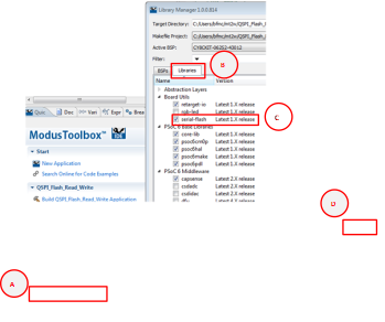
Enable the library in the Library Manager (see Figure 1)
- Select the Library Manager
- Go to the Libraries tab
- Select the Serial Flash Library
- Select Apply
Figure 1. Adding Serial Flash Library
Include the necessary libraries in your application’s main.c file
#include "cyhal.h" /* HAL */
#include "cycfg.h" /* Auto-generated system configuration headers */
#include "cybsp.h" /* Board specific pin and peripheral definitions */
#include "cycfg_qspi_memslot.h" /*QSPI external memory configuration structures */
#include "cy_serial_flash_qspi.h" /* QSPI library functions */
In the
mainfunction, initialize the board peripherals, the UART, and the QSPI block. The QSPI configuration is included in the board support package (BSP) for your kit/* Initialize the device and board peripherals */
result = cybsp_init();
CY_ASSERT(result == CY_RSLT_SUCCESS);
/* Enable global interrupts */
__enable_irq();
/* Initialize retarget-io to use the debug UART port */
cy_retarget_io_init(CYBSP_DEBUG_UART_TX, CYBSP_DEBUG_UART_RX, CY_RETARGET_IO_BAUDRATE);
/* Initialize qspi block and external memory device */
cy_serial_flash_qspi_init(smifMemConfigs[MEM_SLOT_NUM], CYBSP_QSPI_D0, CYBSP_QSPI_D1, CYBSP_QSPI_D2, CYBSP_QSPI_D3, NC, NC, NC, NC, CYBSP_QSPI_SCK, CYBSP_QSPI_SS, QSPI_BUS_FREQUENCY_HZ);Create data buffers to store read and write data. Transfer the data to the external memory. Read back the data and print it to a UART terminal for verification. In the below example, the data is written to and read from the address 0x00040000 in external memory. This address is offset from the base address of external memory, not from the PSoC™ 6 MCU’s local addressing range.
/* Read/write buffers */
uint8 rxBuffer[PACKET_SIZE];
uint8 txBuffer[PACKET_SIZE];
/* Write the content of the txBuffer to the memory */
cy_serial_flash_qspi_write(0x00040000, PACKET_SIZE, txBuffer);

/* Read back after Write for verification */
cy_serial_flash_qspi_read(0x00040000, PACKET_SIZE, rxBuffer);
Using the Peripheral Driver Library
PDL provides a set of functions and structures that access the registers of the QSPI block directly, enabling you to fully configure transactions performed through the QSPI block. This configurability makes the PDL suitable for use in applications where finer control is required.
To get started with the PDL for QSPI using the Eclipse IDE for ModusToolbox™ software, do the following:
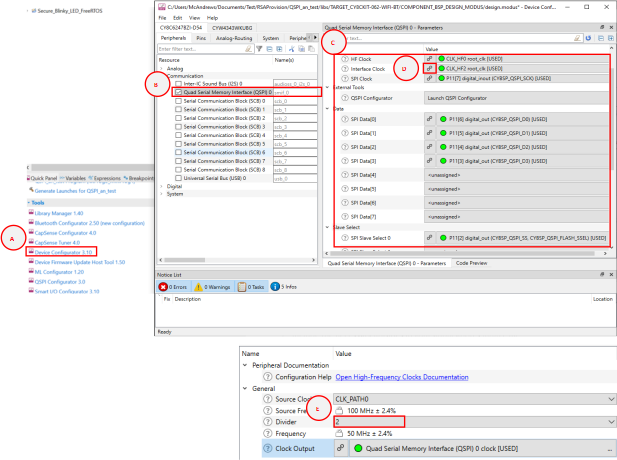
Enable the QSPI hardware using the device configurator. Figure 2 shows an example configuration suitable for use with any PSoC™ 6 MCU kit that has an external flash device.
- Select the Device Configurator from the Quick Panel
- Check the box Quad Serial Memory Interface (QSPI) 0 to enable it
- Configure the QSPI block as shown in Figure 2
- Select the “Go to Signal” button next to Interface Clock to open the clock configuration tab
- Change the clock Divider to 2
- Save your changes and close the device configurator
Figure 2. Steps to configure the QSPI block
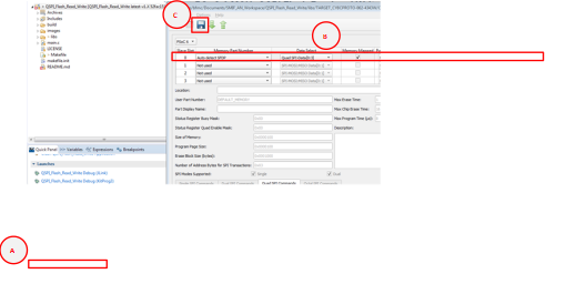
Generate the QSPI configuration structures using the QSPI Configurator. Figure 3 shows an example configuration suitable for use with any PSoC™ 6 MCU kit that has an external flash device.
Note: These instructions describe the process for using an SFDP compliant device. For more information on how to use the QSPI Configurator, including information about how you can generate code for your specific memory configuration, see the QSPI configurator guide.- Select the QSPI Configurator
- Select Auto detect SFDP from the drop-down menu
- Save the configuration
Figure 3. Steps to use the QSPI Configurator
Include the necessary libraries in your application’s main.c file.
#include "cy_pdl.h" /* Peripheral Driver Library */
#include "cybsp.h" /* Board specific pin and peripheral definitions */
#include "cycfg_qspi_memslot.h" /*QSPI external memory configuration structures */
Create a global context variable for the QSPI block.
cy_stc_smif_context_t smif_context;- Define a transaction packet
size
#define PACKET_SIZE (64u) Create an interrupt routine containing a call to the QSPI API interrupt function
Cy_SMIF_Interrupt. All FIFO operations will use this interrupt.void SMIF_Interrupt_User(void)
(
Cy_SMIF_Interrupt(SMIF0, &smif_context);
)In the
mainfunction, initialize the peripherals and global interrupts./* Initialize the device and board peripherals */
result = cybsp_init();
CY_ASSERT(result == CY_RSLT_SUCCESS);
/* Enable global interrupts */
__enable_irq();In the
mainfunction, set up the SMIF interrupts.cy_stc_sysint_t smifIntConfig =
(
#if (CY_CPU_CORTEX_M0P)
/* .intrSrc */ NvicMux7_IRQn,
/* .cm0pSrc */ smif_interrupt_IRQn,
#else
/* .intrSrc */ smif_interrupt_IRQn, /* SMIF interrupt number */
#endif
/* .intrPriority */ 7u
);
(void) Cy_SysInt_Init(&smifIntConfig, SMIF_Interrupt_User);In the
mainfunction, initialize and enable the QSPI block./* SMIF initialization */
Cy_SMIF_Init(SMIF0, &smif_0_config, TIMEOUT_1_S, &smif_context);
Cy_SMIF_Enable(SMIF0, &smif_context); /* Enable the SMIF Interrupt */
#if (__CORTEX_M == 0)
NVIC_EnableIRQ(NvicMux7_IRQn);
#else
NVIC_EnableIRQ(smif_interrupt_IRQn);
#endifIf your external memory supports Serial Flash Discoverable Parameters (SFDP), detect the parameters. For manual memory configuration, this step is optional and only required if you intend to use the device in XIP mode.
    /* Memslot level initialization */
Cy_SMIF_MemInit(SMIF0, &smifBlockConfig, &smif_context);
If your external memory device supports Quad mode, enable Quad mode.
  bool isQuadEnabled = false;
Cy_SMIF_MemIsQuadEnabled(SMIF0, smifBlockConfig.memConfig[0],
                                        &isQuadEnabled,
                                        &smif_context);
Cy_SMIF_MemEnableQuadMode(SMIF0,
              smifBlockConfig.memConfig[0],
              5000,
              &smif_context);
Begin transacting with the external memory device. The following is an example of a write sequence sending data from
txBuffer.uint8_t txBuffer[PACKET_SIZE];
uint8_t rxBuffer[PACKET_SIZE];
/* Erase before write */
Cy_SMIF_MemEraseSector(SMIF0, smifMemConfigs[0],
0x00,
smifMemConfigs[0]->deviceCfg->eraseSize,
&smif_context);
/* Read to rxBuffer after Erase to confirm that all data is 0xFF */
Cy_SMIF_MemRead(SMIF0, smifMemConfigs[0],
smifMemConfigs[0]->deviceCfg->eraseSize,
rxBuffer,
PACKET_SIZE,
&smif_context);
/* Write txBuffer to the external memory */
Cy_SMIF_MemWrite(SMIF0, smifMemConfigs[0],
smifMemConfigs[0]->deviceCfg->eraseSize,
txBuffer,
PACKET_SIZE,
&smif_context);
Features of QSPI
QSPI provides a highly configurable interface between PSoC™ 6 MCU and an external serial memory device. The QSPI block contains several sub-components which enable caching, XIP mode, Command mode, and cryptography.
Figure 4. QSPI block architecture
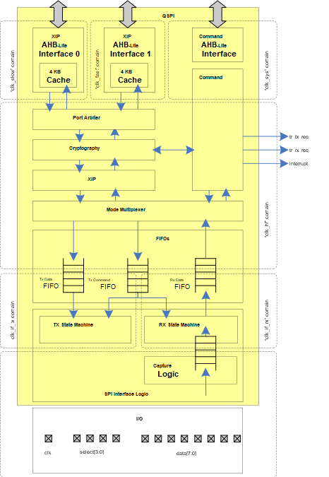
Clock domains
The QSPI block has three AHB-Lite bus interfaces: two for XIP mode and one for Command
mode. The XIP mode interfaces consist of a fast domain and a slow domain. Arm®
Cortex®-M4 is the only bus master in the fast domain. In the slow
domain, Cortex®-M0, Crypto, Datawire0, and Datawire1 can be bus
masters. For Command mode operation, the bus interface is in the clk_sys
domain, which is a divided clock from clk_hf. In Command mode, the bus
master can be any of the bus masters in XIP mode.
The FIFOs in the block work in the SPI interface clock domain. The remainder of the block components, including the cryptography, mode multiplexer, and port arbiter operate in the high frequency clock domain.
Modes
The QSPI hardware provides a mode multiplexer, which allows you to operate the QSPI block
in either Command mode or XIP mode. In the PDL, this mode can be changed during runtime by
calling the Cy_QSPI_SetMode() function. Note that the mode should be
changed only after any ongoing transfers are completed. A call to the
Cy_SMIF_BusyCheck() function should be made to ensure that the QSPI block
is not busy.
Command mode
This is the default mode of the QSPI block and is typically used for large data storage. In
this mode, data transfers are initiated by accessing the FIFOs. Software may transfer
command bytes to the TX command FIFO and data bytes to the TX and RX FIFOs. This mode
generates triggers depending on the number of FIFO entries available or used. The trigger
tr_tx_req is active when the TX data FIFO has fewer entries than specified
by the TX_DATA_FIFO_CTL. TRIGGER_LEVEL field. The trigger
tr_rx_req is active when the RX data FIFO has more entries than specified
by the RX_DATA_FIFO_CTL. TRIGGER_LEVEL field.
Command mode provides the flexibility to implement any SPI transfer, including transfers to configure or erase the external memory. However, in Command mode, your application code must generate the opcode, slave address, dummy cycles, and data. This results in many CPU cycles being spent for each transaction. These extra cycles are not desirable for accessing small amounts of data, such as executing code. However, in this mode, a single transaction can transfer up to 65535 bytes. Hence, Command mode is recommended for bulk data transfers or infrequently accessed data, such as images or other large data types.
XIP mode
This mode is typically used to execute code out of an external memory device. In this mode, the QSPI block automatically generates SPI transfers without software intervention. The external memory space is mapped to a configurable range of addresses in the PSoC™ 6 MCU’s address space through one of the two XIP AHB-lite interfaces. As a result, external memory accesses in XIP mode do not require discrete software intervention and data stored in external memory can be accessed like any other variable.
Caches
The QSPI block also has a dedicated 4 KB cache for each of the XIP interfaces; one for CM4 and another for CM0 and DMA. These caches are enabled by default. Read transfers that hit in the cache are processed by the cache, while read transfers that miss in the cache incur an XIP memory read transfer of 16 bytes to refill the missed subsector. There is also a prefetch buffer, which grabs the next 16 bytes of data to refill the cache. This means that XIP transfers will occur in 32-byte chunks, 16 bytes for the cache and 16 bytes from the prefetch buffer, before a SPI transfer occurs to refill the cache subsector and the prefetch buffer.
As a result, XIP mode is convenient and efficient for small transfers such as executing code out of external memory. For large reads, however, cache and prefetch buffer refills require repeat transmission of the opcode, device address, and dummy cycles every 32 bytes. These refills add latency to the transfer that would not exist in the Command mode.
For RAM devices, XIP mode can write to the external memory. Write transfers in XIP mode bypass the cache and incur a SPI transfer. If a bus master reads and writes to the external memory device, the writes will automatically invalidate the cache.
It is possible for data in the caches to be invalid when data is written to a location in the XIP addressing range. To avoid reading stale data from the caches, you should invalidate the cache when new data is written to the XIP memory region. An example of this would be if you were executing code out of external memory at address 0x18000000 when the QSPI block was transitioned into Command mode and a write occurred at the same address. Switching the block back into XIP mode and executing from that address could cause a failure.
It is also possible for two masters from different AHB clock domains to access the external
memory through the SMIF block, such as the DMA hardware and CM4. In this use case, it is a
good practice to make sure the regions being accessed by each master do not overlap. This
minimizes the likelihood that the cache will contain invalid data. If the accessed regions
do overlap, the cache can be disabled with the PDL function call
Cy_QSPI_CacheDisable() or the cache will need to be invalidated after each
write using Cy_QSPI_CacheInvalidate().
Memory device signal interface
The QSPI block acts as a SPI master when communicating with external memory devices. QSPI only supports SPI configuration 0, where the clock polarity (CPOL) is 0 and the clock phase (CPHA) is 0. In addition, to standard SPI, the block is also capable of operating in Dual-SPI, Quad-SPI, Dual Quad-SPI, and Octal-SPI modes. For all modes, the block operates using Single Data Rate (SDR) mode.
QSPI can support up to four memory devices simultaneously, limited by the number of data select lines. For example, QSPI supports eight data lines, which means that four single or Dual-SPI memory devices can use all eight data lines and all of the available data select lines, or the same four memory devices can use the same data lines but different data select lines. Likewise, four Quad-SPI or Octal-SPI devices can be used simultaneously, sharing data lines but using unique data selects. For a given memory device, the data lines used must be adjacent. To see the signals used by specific memory device types, see Table 1.
| Memory device | I/O signals |
|---|---|
| Single SPI memory | SCK, CS, SI, SO. This memory device has two data signals (SI and SO). |
| Dual SPI memory | SCK,CS, IO0, IO1. This memory device has two data signals (IO0 and IO1). |
| Quad SPI memory | SCK, CS, IO0, IO1, IO2, IO3. This memory device has four data signals (IO0, IO1, IO2, IO3). |
| Octal SPI memory | SCK, CS, IO0, IO1, IO2, IO3, IO4, IO5, IO6, IO7. This memory device has eight data signals (IO0, IO1, IO2, IO3 IO4, IO5, IO6, IO7). |
Each memory device must be mapped to one of the four “slots” in the QSPI block. The slot for your memory device will have a corresponding I/O pin controlling the CS line. To ensure that firmware accesses the correct device, make sure that your QSPI configuration uses the same CS line to which your external memory CS is connected.
For each of the four select lines, there are legal and illegal configurations. Table 2 lists the legal configurations and the corresponding data select enumerated type defined in cy_smif.h. This data set is used automatically when configuring your device using the QSPI Configurator.
cy_en_smif_data_select_t | Single SPI device | Dual SPI device | Quad SPI device | Octal SPI device |
|---|---|---|---|---|
CY_SMIF_DATA_SEL0 | spi_data[0] = SI spi_data[1] = SO | spi_data[0] = IO0 spi_data[1] = IO1 | spi_data[0] = IO0 … spi_data[3] = IO3 | spi_data[0] = IO0 … spi_data[7] = IO7 |
CY_SMIF_DATA_SEL1 | spi_data[2] = SI spi_data[3] = SO | spi_data[2] = IO0 spi_data[3] = IO1 | Illegal | Illegal |
CY_SMIF_DATA_SEL2 | spi_data[4] = SI spi_data[5] = SO | spi_data[4] = IO0 spi_data[5] = IO1 | spi_data[4] = IO0 … spi_data[7] = IO3 | Illegal |
CY_SMIF_DATA_SEL3 | spi_data[6] = SI spi_data[7] = SO | spi_data[6] = IO0 spi_data[7] = IO1 | Illegal | Illegal |
The spi_data values correspond to the QSPI I/O pins on your PSoC™ 6 MCU device. To determine which pins are available as spi_data pins for your device, see the Alternate Pin Function section of the device datasheet.
Dual-quad configurations are also supported by QSPI. In dual-quad configuration, two quad-SPI devices are used simultaneously, with each device contributing a nibble of a byte per transfer. The devices will share the interface clock signal, but will use different CS lines and separate I/O lines. Table 3 lists the configuration for dual-quad mode.
| DATA_SEL[1:0] | Dual-Quad SPI Configuration | ||
|---|---|---|---|
CY_SMIF_DATA_SEL0 | CY_SMIF_DATA_SEL2 | spi_data[0] = IO0 … spi_data[3] = IO3 | spi_data[4] = IO4 … spi_data[7] = IO7 |
For more information about the legal configurations and example diagrams of proper configurations, see the PSoC™ 6 MCU architecture TRM.
Cryptography
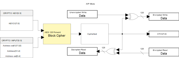
The QSPI block includes a cryptography component to make sure data can be securely stored in external memory. The encryption and decryption are based on the AES-128 forward block cypher. A 128-bit key, stored in dedicated write-only QSPI registers SMIF_CRYPTO_KEY3, …, SMIF_CRYPTO_KEY0, is used with a 128-bit plaintext to generate a cyphertext. The method of generating the cyphertext depends on whether the QSPI block is in Command or XIP mode.
The Serial Flash Library does not support encryption, so the PDL functions for encryption must be used. If you prefer the Serial Flash Library for configuration and data transfers, a combination of Serial Flash Library and PDL can be used.
Cryptography in XIP mode
In XIP mode, the cryptography component supports on-the-fly encryption and decryption, which is applied automatically on the code executed from an external memory or data written to or read from an external RAM. The encryption uses AES-128 encryption algorithm with your key on input data called a plaintext. The plaintext in XIP mode is the 28-bit XIP address extended to 128 bits with the contents of the SMIF0_CRYPTO_INPUT registers.

Figure 5 shows the format of the extended address.
Figure 5. Extended address used in XIP cryptography

After applying AES-128 with your key on the extended address, the resulting cyphertext is XOR’d with the transfer’s read or write data. By applying AES-128 to the address rather than the data being transferred, the encryption and decryption occur on-the-fly and cause no delay. Figure 6 shows the entire encryption process in XIP mode.
Figure 6. On-the-fly encryption process for XIP mode
To enable encryption in XIP mode, set the SMIF0_DEVICEn_CTL.CRYPTO_EN bit, where DEVICEn refers to the memory slot of your external memory device. For example, to enable encryption on a memory device in slot 2, use the following line of code:
SMIF0->DEVICE[2].CTL |= (1 << SMIF_DEVICE_CTL_CRYPTO_EN_Pos /* 8U */);
To disable encryption, clear the CRYPTO_EN bit.
Cryptography in Command mode
Command mode cryptography can be used to encrypt bootloaders, application images, or bulk
data in external flash memories. Encryption in Command mode requires discrete calls to the
PDL encryption function, Cy_SMIF_Encrypt,for each data transfer. The
resulting cyphertext is stored in the CRYPTO_OUTPUT registers and must be unpacked before
writing the data to external memory, but this is handled inside the
Cy_SMIF_Encrypt function automatically. For compatibility with XIP
on-the-fly decryption, the Cy_SMIF_Encrypt function uses the same
encryption scheme used in XIP mode encryption.
For Command mode, the encryption flow should generally follow these steps:
- Make sure you have loaded your encryption key into the SMIF_CRYPTO_KEY registers.
- Encrypt the data to be transferred using the PDL function
Cy_SMIF_Encrypt. - Write the data to the external memory.
For decryption:
- Read the encrypted data from the external memory.
- Decrypt the data using the PDL function
Cy_SMIF_Encrypt.
Ecosystem
The QSPI block has an ecosystem of tools and files consisting of:
- ModusToolbox™ Application Software libraries
- The QSPI Configurator tool
- Programming tools
Figure 7 shows the various components of the ecosystem and the files used or generated by those components.
Figure 7. QSPI ecosystem of tools
ModusToolbox Application Software
libraries
The ModusToolbox™ Software Environment includes the libraries and files necessary to use QSPI without the need to access the hardware registers directly. The PDL provides low-level configuration for the QSPI block and the API necessary to transfer data to the memory device. The Serial Flash Library and the HAL provide layers of access above the PDL. Table 4 lists the files used by these libraries and the library to which they belong.
| File | Description | Library |
|---|---|---|
| cy_smif.c/h | Provides the low-level API for configuring the QSPI hardware and initiating transfers. Used to directly configure the QSPI block. | PDL |
| cy_smif_memslot.c/h | One level above cy_smif.c. Provides the low-level API for accessing external memory, including status registers and SFDP parameters. Typically used in command mode or for SFDP detection, but also defines memory device status checking functions. | PDL |
| cyhal_qspi.c/h | Abstracts out any chip specific configuration functions. Functions in the HAL automatically set up the pins used by the block, any required interrupts, and timeouts for each data transfer. Typically used in conjunction with the Serial Flash Library for high-level memory access. | HAL |
| cy_serial_flash_qspi.c/h | Provides wrappers around functions from both cy_smif.c and cy_smif_memslot.c to ease the use of QSPI. Uses the HAL to set up chip-specific configurations. Functions included in these files limit configurability, but are simple to use and provide the functions needed for most memory accesses. | Serial Flash Library |
| cy_serial_flash_prog.c | Provides the variables necessary to instruct the programming tools how to program an attached serial flash memory. Depends on files generated in the QSPI Configurator Tool. Typically used with XIP mode to expose external memory addresses for programming. | Serial Flash Library |
QSPI Configurator tool
The ModusToolbox™ Software Environment includes the QSPI Configurator. The Configurator tool provides a simple graphical interface to set up QSPI to use an external memory device. You can launch the Configurator from within ModusToolbox™ IDE, following step 1 from Using the Peripheral Driver Library. You can also launch the standalone Configurator tool to generate source files that can be used in most IDEs. Navigate to your ModusToolbox™ installation folder and follow this path:
(Install Dir)\ModusToolbox\tools_2.0\qspi-configurator\qspi-configurator.exe
In the Configurator, you can select your memory device, slot or select line it is connected to, SPI width, memory address ranges, and encryption (for XIP mode). Once you have set your choices, the QSPI Configurator tool automatically generates the source and header files containing the parameters of your external memory device. The parameters of the device are stored in configuration structures, which can be passed as arguments to the PDL or Serial Flash Library functions to easily access your memory device.
| File | Description |
|---|---|
| cycfg_qspi_memslot.c/h | Automatically generated from the QSPI Configurator. Provides the definitions for the QSPI Memory device configuration, or sets up default structures for SFDP detection. |
The Configurator tool pulls configurations from a database of memory files in XML format, called .cymem files. These files, and an editable template memory file, are typically installed along with the ModusToolbox™ IDE. For more information on these files and how to use the QSPI Configurator Tool, see the user guide.
Programming tools
The QSPI block supports programming of external memories through programming tools such as the KitProg3 provided with Infineon kits. For detailed information about how to setup your application to support external memory programming, see Programming external memory.
Configuration
QSPI configuration structure architecture
To access an external memory device, you need to make sure your QSPI block is configured correctly for the memory device that you are using. The cycfg_qspi_memslot.c/h files generated by the QSPI Configurator tool provides a set of nested structures that contain each configuration parameter for your system. This reduces the amount of time you need to spend on creating command lists and setting up the transfer parameters for each transfer. Figure 8 shows organization of the generated structures.
Figure 8. QSPI configuration structure architecture
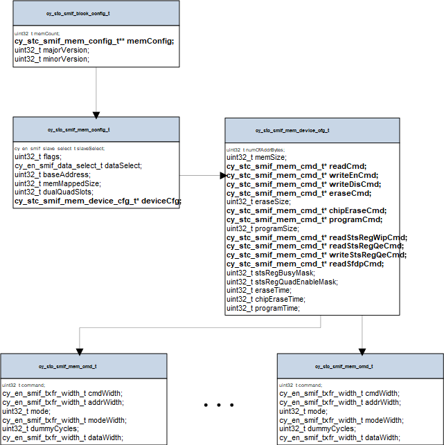
At the highest level is the cy_stc_smif_block_config_t structure. This
simple structure contains the number of memory devices connected to the block, the QSPI
driver version, and a double pointer to the memory configuration structure.
Nested within the block configuration structure is the memory configuration structure. This structure contains application-level information about the external memory device, including the SPI slave select slot, the slot of the data lines, the base address, the size of the external address, the number of dual-quad SPI slots, and a pointer to the memory device configuration structures.
The memory device configuration structure,
cy_stc_smif_mem_device_cfg_t,contains device-specific information
including the default memory commands necessary to access the memory device. Typically, the
details of this structure can be filled in using information from your memory device’s
datasheet.
The lowest level structure within the overall QSPI architecture is the memory device
command structure, cy_stc_smif_mem_cmd_t. For each of the commands listed
in the memory device configuration structure, there is a corresponding command structure.
These structures specify the requirements of the commands, including command width, address
width, mode, mode width, data width, and the number of dummy cycles.
Configuration procedure
SFDP detection
The serial flash discoverable parameter (SFDP) standard provides a set of standard parameter tables that define the capabilities and access specifications for serial flash devices. These tables are internal to serial flash devices that use the SFDP standard and can be read from to determine the settings required to access the device.
The QSPI block supports SFDP detection. For all devices that support this functionality, it is recommended that you enable SFDP detection to simplify configuration. Using SFDP detection will automatically populate the QSPI configuration structures mentioned in QSPI configuration structure architecture.
You can configure the QSPI block to perform SFDP detection in the QSPI Configurator tool. Follow the steps in QSPI Configurator and launch the QSPI Configurator tool. From the Memory Part Number drop-down menu, select Auto detect SFDP, as Figure 9 shows. Make sure your selection is in the slave slot that corresponds to your hardware connection.
Figure 9. SFDP detection with QSPI configurator

Choosing this option will generate the configuration structures with the prefix “Auto_detect_SFDP”, and default values as set in the Configurator tool.
cy_stc_smif_mem_config_t Auto_detect_SFDP_SlaveSlot_0
In your application, a call to the Cy_SMIF_MemInit function will perform the SFDP detection and populate the structures with the detected parameters.
Manual configuration
If your device does not support SFDP or to manually configure your device settings, you can select a supported part number from the Memory Part Number drop-down menu.
For custom or unsupported devices, you can either create a new memory file (*.cymem) to get support in the Configurator tool, or you can manually populate the structures in the source file (cycfg_qspi_memslot.c/.h) with your device’s parameters.
To create a new memory file, follow the steps outlined in the QSPI Configurator Guide under the section “Create New Memory File”.
Order of operations
When using the PDL or Serial Flash Library, it is important to keep in mind that the functions take care of several important transfer steps automatically. For write transfers, this is typically a two-step process that involves transmitting a write enable command followed by a program command. For read accesses, a read command is usually the only necessary step.
After commands that transfer data, it is important to make sure that the data transfer is complete and the external memory device is ready for the next transaction before using the QSPI block again. This is handled within functions in cy_smif_memslot.c/h, however, for lower level PDL accesses, you can use the function Cy_SMIF_GetTransferStatus() to determine the current status of the transfer. You can also transmit a device-specific status command using the Cy_SMIF_TransmitCommand() function to read the status of the external memory device. To determine the correct read status command for your device, see the device datasheet.
Additionally, many external memory devices require an erase or erase sector operation before writing to the memory device. This can be accomplished by transmitting the device-specific erase command or by using functions provided in the cy_smif_memslot.c/h files, the Serial Flash Library files, or the HAL.
The typical flow for a write data transfer follows these steps:
- Checks that the external memory is not busy
- Transmits the write enable command
- Erases the sector of the external memory device that you are going to write to
- Waits for the external memory erase to finish, this may take a long time. See your memory device datasheet for erase time specifications.
- Transmits the write enable command to the external memory device
- Programs the data into the external memory
- Waits for the transfer to complete
- Waits for the external memory device to be ready
A read transfer is simpler, requiring only the read command and a check for the transfer to be complete.
- Checks that the external memory is not busy
- Transmits the read command at the address of the data to be read
- Waits for the transfer to be complete
Programming external memory
QSPI supports programming of external memory through programming tools such as the OpenOCD or the KitProg3 device included on PSoC™ 6 MCU kits. To enable this feature, several important steps should be followed or the programming may fail.
Figure 10. External memory programming flow
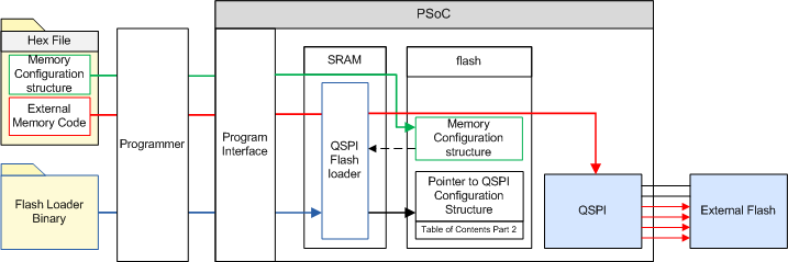
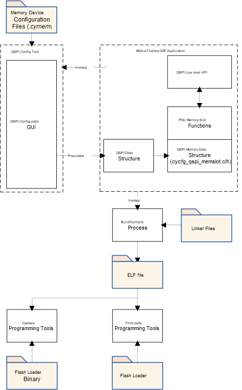
In Figure 10, the red arrows represent the code or data that is going to be programmed into the external memory through the QSPI interface. Before the code or data makes its way into the external flash, it must travel through the programmer, the programming interface, the QSPI flash loader, and then finally into the QSPI interface.
At the end of the programming process, the QSPI flash loader is programmed into the PSoC™ 6 MCU SRAM and begins to execute. The flash loader attempts to find a pointer to the QSPI configuration structure from a fixed location in flash as part of the Table of Contents part 2 (TOC2) structure. It is your responsibility to place the pointer in this location so that the flash loader can find it and have the command structure for programming external memory.
To do this, follow these steps:
If you are using the Serial Flash Library, navigate to the cy_serial_flash_prog.c file and add the definition
#define CY_ENABLE_XIP_PROGRAM. This automatically includes the necessary pointer in the correct location in flash. No further steps are required.If you are not using the Serial Flash Library, create a structure which contains a pointer to the cy_stc_smif_block_config_t structure and a NULL termination.
typedef struct
(
    const cy_stc_smif_block_config_t * smifCfg; /* Pointer to SMIF top-level configuration */
    const uint32_t null_t; /* NULL termination */
) stc_smif_ipblocks_arr_t;
Create an instance of this structure and place it in a known location.
CY_SECTION(".cy_sflash_user_data") __attribute__( (used) )
const stc_smif_ipblocks_arr_t smifIpBlocksArr = (&smifBlockConfig, 0x00000000);
Place your structure into the TOC2 in the following manner. This structure is a predetermined fixed location in flash known to the flash loader.
CY_SECTION(".cy_toc_part2") __attribute__( (used) )
const uint32_t cyToc[128] =
(
0x200-4,                /* Offset=0x0000: Object Size, bytes */
0x01211220,             /* Offset=0x0004: Magic Number (TOC Part 2, ID) */
0,                      /* Offset=0x0008: Key Storage Address */
(int)&smifIpBlocksArr,  /* Offset=0x000C: This points to a null terminated array of SMIF structures */
0x10000000u,            /* Offset=0x0010: App image start address */
                /* Offset=0x0014-0x01F7: Reserved */
[126] =  0x000002C2,    /* Offset=0x01F8: Bits[1:0] CLOCK_CONFIG(0=8MHz, 1=25MHz, 2=50MHz, 3=100MHz)
                                  Bits[4:2] LISTEN_WINDOW(0=20ms,1=10ms,2=1ms,3=0ms,4=100ms)
                                  Bits[6:5] SWJ_PINS_CTL (0/1/3=Disable SWJ, 2=Enable SWJ)
                                  Bits[8:7] APP_AUTHENTICATION (0/2/3=Enable, 1=Disable)
                                  Bits[10:9] FB_BOOTLOADER_CTL: UNUSED */
[127] =  0x3BB30000     /* Offset=0x01FC: CRC16-CCITT (the upper 2 bytes contain the CRC and the lower 2 bytes are 0) */
);
For more information about the TOC2, its use, and its contents, see the device architecture TRM.
Additionally, the QSPI flash loader does not perform SFDP detection. This means that you must make sure your device is manually configured and the configuration is stored in flash. To do this using the QSPI Configurator tool, select your memory part from the Memory Part Number drop-down menu and make sure the option Config Data in Flash is selected.
Figure 11. Example configuration for external memory programming

In your firmware, you can then begin placing functions or variables at locations within the external memory addressing range. To do this, you can use the attribute CY_SECTION(".cy_xip") __attribute((used)) before a variable or function declaration to place the value in the external memory region.
Security with QSPI
If you are using QSPI to store sensitive data or proprietary libraries, you need to secure your QSPI system. Using the cryptography, explained in Memory device signal interface, is helpful in protecting the data itself, but it does not prevent you from reading out the encrypted data or from injecting other code into an XIP section.
Several important steps are required to secure your QSPI system. The first step is to make sure you are encrypting your data, either through the QSPI provided encryption or through some other robust method. This protects the data itself, making it difficult for a hacker to read sensitive information.
Your next layer of security should come from protecting the QSPI register space from read and write access. This will prevent a hacker from switching the QSPI block mode from XIP to command mode and reading out the encrypted data during runtime. This will also prevent modification of your cryptography key. To do this, make sure your cryptography key is correct and any executable code for the external memory is encrypted and programmed into the external memory device. Then, you can use a Peripheral Protection Unit (PPU) to set the access restrictions for your QSPI block, allowing you to configure read/write restrictions for registers in the QSPI block.
For applications using XIP mode, the code in the external memory also needs to be protected. Because this memory can be shared and accessed by multiple masters (for example, DMA and a CPU) a Shared Memory Protection Unit (SMPU) should be used. The SMPU will allow you to configure the region base address, the size of the memory to protect, and the access restrictions for the memory region. By default, the external memory region is 0x18000000, however, this can be changed in the QSPI Configurator tool.
Finally, make sure that any code stored in the external memory region is validated along with the rest of your application image. For more information on code signing and secure system architecture with PSoC™ 6 MCU, see AN221111.
Performance
Serial memory devices are often used as external memory devices for frame buffers or frequently accessed memory like an EEPROM. In these cases, it is important to have low latency transfers with high throughput. The QSPI block follows the SPI protocol for command mode transfers or for transfers in XIP mode where there is a cache miss. In these cases, the latency of a transfer is given by Equation 1.
When encrypting data in command mode, the encryption process takes roughly 13 clk_hf cycles, meaning that as long as your calculated transfer time is greater than 13 cycles you will not see a delay.
For XIP mode with caching enabled, any access that hits in the cache will be processed by the cache. Keep in mind that the cache is 16 B and the prefetch buffer is the contiguous 16 B directly following the cache, so every 32 B of contiguous access will incur a single refill for the next 32 B. This refill will behave similarly to a Command mode transfer and can be calculated using the above equation. This makes XIP mode accesses suitable for short read or execute accesses, but for larger read accesses the extra cycles from the repeated refills add an undesirable delay. Thus, for larger data transfers Command mode is advised.
Encryption in XIP mode occurs on-the-fly and does not cause any latency.
Summary
This application note explained how to use the PSoC 6 MCU QSPI block to access external memory devices. It provided a simple reference flow, explained the features in the block, discussed security design requirements, and performance of the block. For lower-level details about the architecture of the QSPI block within PSoC 6 MCU, see the architecture TRM. Additionally, there are many code examples demonstrating how to use external memories with QSPI. See Related documents for these examples.
Related documents
For a comprehensive list of PSoC 6 MCU resources, see KBA223067 in the community. For a comprehensive list of PSoC 3, PSoC 4, and PSoC 5LP resources, see KBA86521 in the community.
| Application notes | ||
|---|---|---|
| AN210781 – Getting Started with PSoC 6 MCU with Bluetooth Low Energy (BLE) Connectivity | Describes PSoC 6 MCU with Bluetooth® Low Energy Connectivity devices and how to build your first PSoC Creator project | |
| AN221774 – Getting Started with PSoC 6 MCU | This application note helps you explore PSoC 6 MCU architecture and development tools, and shows how to create your first project using ModusToolbox™ and PSoC Creator | |
| AN215656 – PSoC 6 MCU: Dual-CPU System Design | Describes the dual-CPU architecture in PSoC MCU, and shows how to build a simple dual-CPU design | |
| AN219434 – Importing PSoC Creator Code into an IDE for a PSoC 6 MCU Project | Describes how to import the code generated by PSoC Creator into your preferred IDE | |
| Code examples | ||
| CE220823 – PSoC 6 MCU SMIF Memory Write and Read Operation | This example demonstrates the write and read operations to the Serial Memory Interface (SMIF) in PSoC 6 MCU | |
| CE222460 – SPI F-RAM Access Using PSoC MCU SMIF | CE222460 provides a code example that implements the SPI host controller on PSoC 6 MCU using the SMIF Component and demonstrates accessing different features of the SPI F-RAM | |
CE228954 – PSoC 6 MCU QSPI flash read and write using SFDP | This example demonstrates interfacing with an external NOR flash memory in Quad-SPI mode using the Serial Memory Interface (SMIF) block in PSoC 6 MCU . This example uses the Serial Flash Discoverable Parameters (SFDP) standard to auto-discover the flash parameters and the commands for read, program, and erase operations. | |
| Device documentation | ||
| PSoC™ 6 MCU Datasheets | ||
| PSoC™ 6 MCU Technical Reference Manuals | ||
| PSoC™ 6 MCU Programming Specifications | ||
| Development kit documentation | ||
| CY8CKIT-062-BLE, PSoC™ 6 BLE Pioneer Kit | ||
| CY8CKIT-062-WIFI-BT, PSoC™ 6 WiFi-BT Pioneer Kit | ||
| CY8CPROTO-062-4343W, PSoC™ 6 WiFi-BT Prototyping Kit | ||
| CY8CPROTO-063-BLE, PSoC™ 6 BLE Prototyping Kit | ||
| Tool documentation | ||
| ModusToolbox™ IDE | Look in <ModusToolbox install folder>/doc | |
Revision history
| Document version | Date of release | Description of changes |
|---|---|---|
| ** | 2020-03-10 | New application note. |
| *A | 2021-03-08 | Updated to Infineon template. |
| *B | 2022-05-16 | Updated Figure 2. |
| *C | 2023-04-20 | Updated hyperlinks. |