AN219528 PSoC™ 6 MCU low-power modes and power reduction techniques
About this document
Scope and purpose
AN219528 describes how to use PSoC™ 6 MCU power modes to optimize power consumption. Major topics include low-power modes in PSoC 6 MCU devices, and power management techniques using PSoC 6 MCU features. Associated code examples demonstrate different low-power techniques. See AN230938 – PSoC 6 MCU low- power analog for additional information on the low-power analog peripherals of CY8C62x4 family devices.
More code examples? We heard you.
To access an ever-growing list of hundreds of PSoC MCU code examples, please visit our code examples web page. You can also explore the video training library here.
Introduction
PSoC™ 6 MCU gives the best power-saving benefit when low-power modes are implemented with other power-saving features and techniques, without significantly sacrificing the performance. This application note describes not only general power-saving methods but also the unique low-power modes in PSoC™ 6 MCU. It also discusses other low-power considerations.
This application note requires a basic knowledge of the PSoC™ MCU architecture, and the ability to develop a PSoC™ 6 MCU application using ModusToolbox™ software. If you are new to PSoC™ 6 MCU, see AN221774 - Getting started with PSoC™ 6 MCU or AN228571 – Getting started with PSoC™ 6 MCU on ModusToolbox™ software.
If you are designing an Internet of Things (IoT) system, there are additional connectivity-related power considerations that impact total system power. While these considerations are outside the scope of this application note (AN), there are specific application notes focused on low-power IoT systems. AN227910 – Low- power system design with AIROC™ CYW43012 Wi-Fi & Bluetooth® combo chip and PSoC™ 6 MCU discusses optimizations for low power in Wi-Fi, Bluetooth®, and PSoC™ 6 MCU systems.
Power modes
Power mode transitions
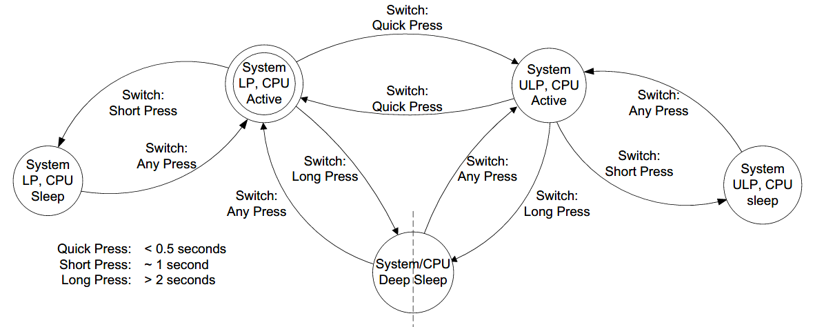
PSoC 6 MCU features seven power modes that are divided into system modes that affect the whole device, and standard ARM® CPU modes that affect only one CPU. The system power modes are Low-Power (LP), Ultra-Low-Power (ULP), deep sleep, and hibernate. The ARM® CPU power modes are active, sleep, and deep sleep; these are available in system LP and ULP power modes. Table 1 lists the power modes in which the devices operate.
| Power mode | Description |
|---|---|
System LP |
|
System ULP |
|
CPU active |
|
CPU sleep |
|
CPU deep sleep |
|
System deep sleep |
|
System hibernate |
|
Figure 1 shows how power mode transitions are based on different events and actions, including interrupts, firmware actions, and reset events. In some cases, mode transitions are done through multiple modes.
For more detailed information, see PSoC™ 6 MCU architecture technical reference manual and Power modes summary.

CPU sleep and wakeup instructions
ARM® Cortex® CPUs transition between sleep and wakeup independently. Figure 2 shows several scenarios of wakeup from sleep.
Wait-for-Interrupt (__WFI) is the core sleep
instruction. After a CPU executes __WFI, the CPU goes
to sleep and stays in sleep until any interrupt is asserted. Wait-for-Event
(__WFE) is similar to
__WFI, but it wakes up when the wakeup event is
received instead of an interrupt. Set Event (__SEV) is
used for waking up other CPUs in sleep mode because of a
__WFE. CPU deep sleep uses the same instructions for
sleep and wakeup, but the SLEEPDEEP bit[2] of the Arm® System Control Register (SCR) is set before a sleep instruction. For more
information on SCR, see ARM® system control register user guide. This process is implemented
in SysPm PDL library and HAL APIs.
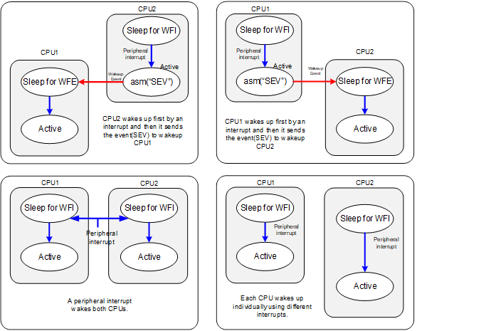
CPU power modes are different from system power modes. Figure 2 shows that each CPU supports its own sleep modes, independent of the state of the other CPU. The device is in system deep sleep mode when both CPUs are in deep sleep. For more detailed information, see AN215656 – PSoC™ 6 MCU dual-CPU system design.
Low-power assistant
Low-power assistant features
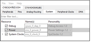
The low-power assistant (LPA) provides an easy-to-use GUI for setup of both device and system power options. The LPA’s goal is to aid in quickly attaining datasheet power numbers in real-world user applications. For each power option supported in the device, the ModusToolbox™ device configurator has corresponding sections to configure power resources in the same method as configuring any other peripheral.
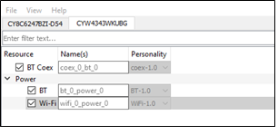
To launch the assistant, for PSoC™ 6 MCU devices, from under the PSoC™ 6 MCU part number tab and System sub-tab, select Power resource, as shown in Figure 3. For connectivity devices, from under the Wi-Fi or Bluetooth® device part number tab, select the BT or Wi-Fi Resource in the Power section, as shown in Figure 4. See the LPA documentation in the Documentation section located at the top of the Power Configurator.
PSoC™ 6 MCU device LPA settings
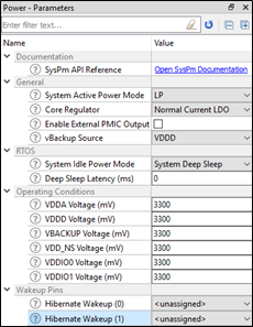
Use the PSoC™ 6 MCU device section of the LPA to configure the initial power configuration of the device as shown in Figure 5. Use the General section of the LPA to configure the highest power settings required in the design for system power mode, core regulators, and Vbackup domain features. After the highest power mode is configured, use the RTOS section to configure the lowest power mode the system automatically transitions into. In many designs, this is all the power mode configuration required, because the RTOS typically handles all the dynamic mode transitions. For more advanced use cases, the HAL or SysPm PDL library power functions can be called at any time to dynamically modify any of the power settings or initiate a power mode transition.
CPU and system wakeup from sleep and deep sleep power modes occur when any configured peripheral interrupt is triggered. You can configure the sleep and deep sleep wakeup interrupts by enabling the desired wakeup peripheral’s interrupt in that peripheral’s configurator within ModusToolbox™ device configurator. If your system enters hibernate mode at runtime using HAL or SysPm calls, the LPA Wakeup pins section simplifies the selection of hibernate wakeup sources.
Connectivity device LPA software settings
Use the “Connectivity device” section of the LPA software to configure Wi-Fi and Bluetooth® power options. AIROC™ Bluetooth connectivity devices are designed to automatically operate in their lowest power modes. The primary power option is to enable the Bluetooth device host wakeup trigger as shown in Figure 6. Bluetooth host wakeup allows the PSoC 6 MCU host device to enter a system deep sleep or hibernate mode and wait for the Bluetooth connectivity device to wake up the MCU by generating a GPIO pin interrupt when it is required to process Bluetooth operations.

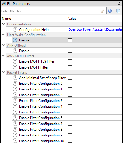
Infineon AIROC Wi-Fi & Bluetooth® connectivity devices support a wide range of power optimization techniques that you can configure based on the needs of the application and network features supported, as shown in Figure 7. The three primary low-power features for Wi-Fi are host wakeup, offloads, and filters.
- Host wakeup allows the PSoC 6 MCU host to enter system deep sleep or hibernate mode until the Wi-Fi device requires MCU processing. When the host MCU must wake up, the Wi-Fi device triggers a GPIO pin interrupt. A host wakeup is required to use most of the other low-power Wi-Fi features
- Offloads allow the MCU’s device stack processing to be moved (offloaded) to the Wi-Fi device internal processor. This increases the time the MCU host can devote to other tasks or spend in a low-power mode
- Filters run on the Wi-Fi device and avoid waking the host MCU until the filter conditions are met. An example is an IoT device that needs to respond only to MQTT packets. The device can enable MQTT filters to ignore all other network traffic allowing the host MCU device to stay longer in a low-power mode
Subsystem availability and power consumption
Subsystem availability
Each subsystem resource works differently in various system power modes. For example, the CPU can be in ON, OFF, and Retention modes. It is important to select proper peripherals for the power mode to work correctly. Table 2 lists the resources available in different power modes.
Approximating power consumption
See the device datasheet for power consumption data for given conditions. Because there are different combinations to achieve the best power consumption, the actual power consumption of the application can be different from the datasheet.
Example case scenarios
Proper power mode selection reduces power consumption without performance degradation. Table 2 lists sample scenarios of power modes. In some examples, only a few power modes are used effectively.
| Power modes | Wearable device | Air conditioner | Remote controller | Thermometer |
|---|---|---|---|---|
System LP CPU active | GUI interaction by user | Motor run | – | Communicates over BLE |
System ULP CPU active | Processes heartbeat | – | Sends command | Reads temperature Updates result on LCD |
System LP CPU sleep | – | – | – | – |
System ULP CPU sleep | Analog block detects heartbeat | – | – | – |
System deep sleep | Goes to deep sleep when the device does not detect heartbeat for 30 seconds (device is not in use) | Waits for command No motor run Wakeup by infra-red (IR) triggering | – | Wakes up every 1 second using watchdog timer (WDT) |
System hibernate | Low battery – Does nothing Resets device when charger is plugged in | – | Waits for button press | – |
System power management (SysPm) library
Overview
HAL
The hardware abstraction layer (HAL) provides an interface for changing power states.
Using the HAL library's APIs, users can achieve all supported CPU power states (active, sleep, and deep sleep) as well as system power states (normal, low, and hibernate).
The library also provides an option to register (or unregister) a callback function(s) to be called on requested power state transitions.
The ability to enter deep sleep can be locked using the APIs and then released once the critical block execution is complete.
PDL
The peripheral driver library (PDL) is a complete software tool that includes APIs for configuring peripherals and system registers to implement the desired functionality. PDL provides direct access to almost all hardware resources of the target device. It reduces the need to understand and directly access registers and bit structures.
Within the PDL, the system power management (SysPm) API provides functions to change power modes as shown in Figure 1. The API can also register callback functions to execute a peripheral function before or after power mode transitions as shown in Figure 8. PDL is downloaded from GitHub while creating an application in ModusToolbox™ using the Project Creator tool, and it is not installed along with theModusToolbox™ IDE.
Mode transition functions
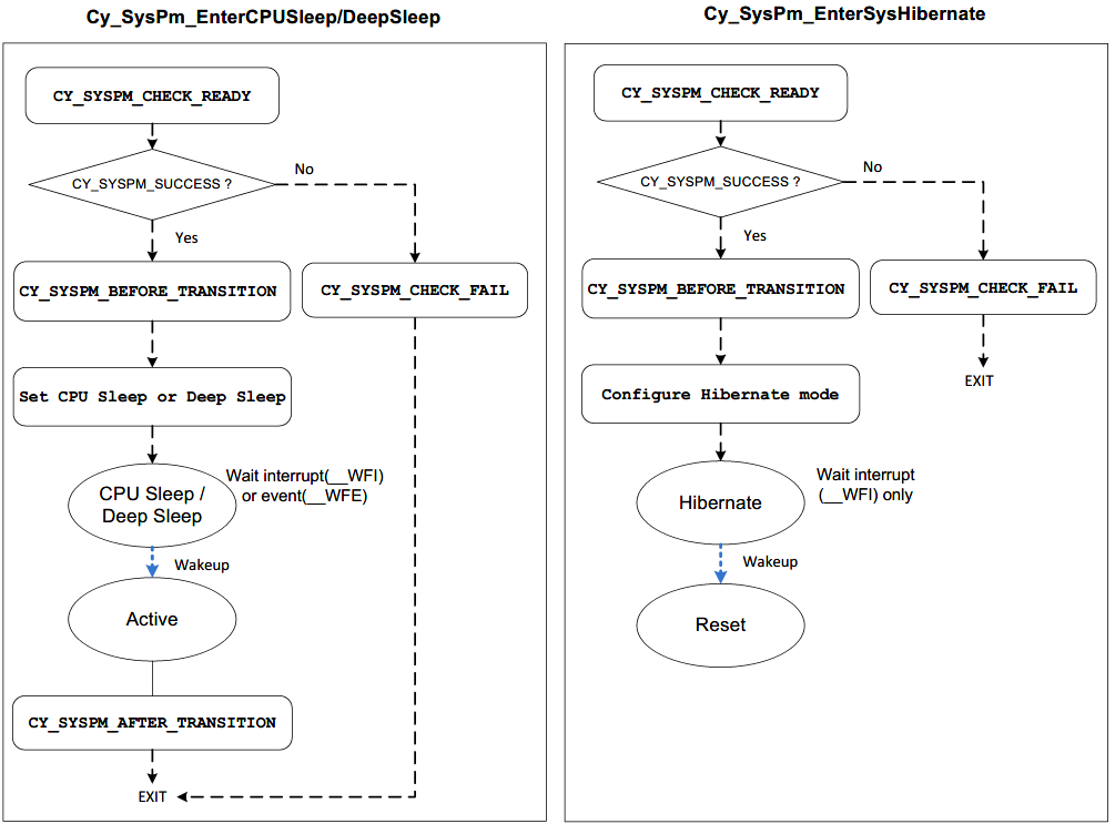
Figure 1 shows firmware transitions for power modes. SysPm provides the default five transition functions for CPU sleep, CPU deep sleep, system hibernate, system LP, and system ULP.
The power mode changing functions provide four different callback operations to execute a necessary action for each peripheral:
| Callback function | Description |
|---|---|
CY_SYS_PM_CHECK_READY | Checks the ready state to transition to other mode. Exits without
transition if it returns
CY_SYSPM_FAIL. |
CY_SYSPM_BEFORE_TRANSITION | Callbacks execute and configure required actions before mode transition. |
CY_SYSPM_AFTER_TRANSITION | Callbacks execute after mode transition or configuration. |
CY_SYS_CHECK_FAIL | Callbacks execute only when
CY_SYSPM_CHECK_READY fails. It executes
the rollback action. |
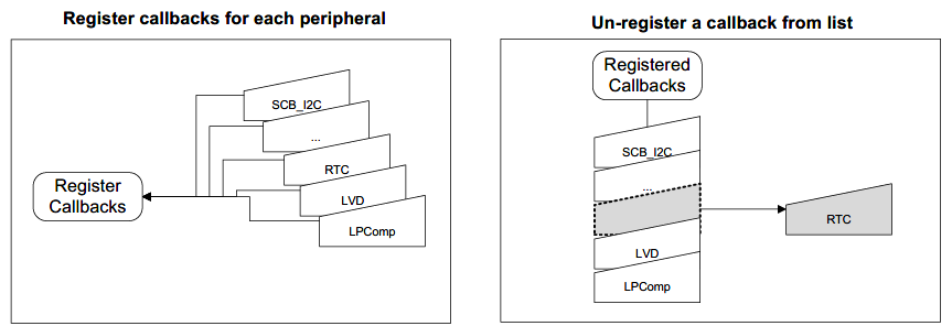
The SysPm driver provides three functions for callback: registration, de-registration, and execution. These functions not only help in power optimization, but also in preventing an abnormal peripheral state after mode transition. The PDL and HAL expect the user to register callbacks for each power mode, as shown in Figure 8. Most peripheral drivers have predefined callbacks associated with each power mode. You can choose to register the defined peripheral callback or can make a custom callback. The SysPm transition function executes the registered callbacks sequentially. The first registered function is executed first.
By calling the mode transition function, the device starts to transition
with four callback operations. The CPU sleep and CPU deep sleep modes use Arm® sleep instructions. Code execution stops and
waits for an interrupt during the CPU sleep power mode. Figure 8 shows the CPU waiting for a
wakeup source after calling the sleep instruction:
__WFI() or __WFE().
After wakeup, the device automatically transitions to CPU active.
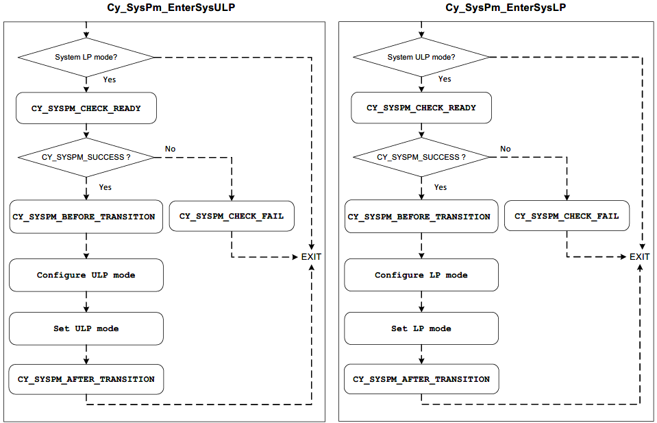
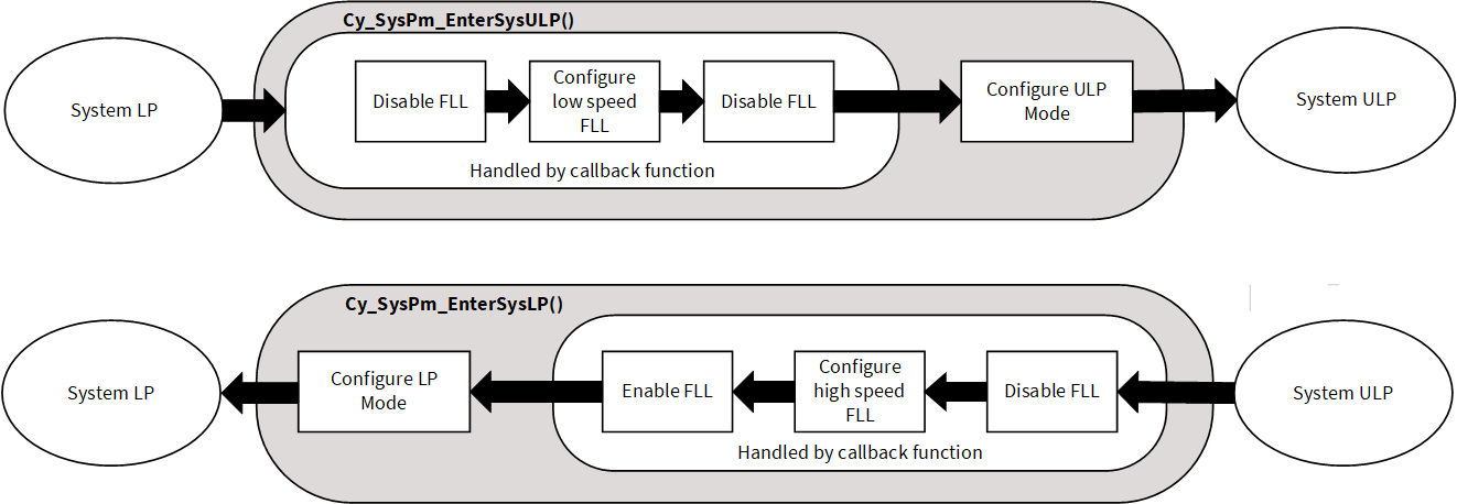
In the system LP and system ULP modes, all system resources keep running. Entering system LP and ULP modes is done by configuring the power mode control register; the transition occurs without delay. SysPm PDL and HAL provide the associated driver functions, as shown in Figure 10. For the best power efficiency, it is necessary to configure the core voltage regulator and the system clock. For more detailed information, see Core voltage selection, ULP mode clock and peripheral driver library documentation (PSoC™ Creator > Help > Documentation > Peripheral Driver Library).
PSoC 6 MCU power management
Core voltage selection
Linear regulator and buck regulator
PSoC™ 6 MCU supports multiple on-chip regulators including low drop out (LDO) and single input multiple output (SIMO), or single input single output (SISO) buck to generate VCC for core power, as listed in Table 3. The LDO can provide up to 300 mA in high-current mode (normal) and 25 mA in low-current mode. The buck regulator can provide up to 20 mA for one output and 30 mA combined for both outputs of the SIMO buck. The SIMO buck regulator provides better efficiency under normal load conditions. Once switched to the SIMO buck regulator, it is not possible to switch back to the LDO without resetting the device.
| Output | Max load | Max clock frequency | |
|---|---|---|---|
| LDO | 0.9 V | 25/300 mA (low-current mode/normal mode) | 50 MHz for Arm® Cortex®-M4 (CM4) 25 MHz for Arm® Cortex®-M0+ (CM0+) |
| 1.1 V | 25/300 mA (low-current mode/normal mode) | Allow maximum supportable clock frequency | |
| Buck | 0.9 V | 20 mA | 50 MHz for CM4 25 MHz for CM0+ |
| 1.1 V | 20 mA | Allow maximum supportable clock frequency |
ULP mode clock
Transition to ULP mode can be done by configuring the power mode control register. There is a maximum clock speed limitation in ULP mode as described earlier, so the clock configuration should be adjusted based on the regulator output when entering or exiting ULP mode. PDL provides associated functions to configure the PWR_CTL register. For more information, see PSoC™ 6 MCU registers technical reference manual.
Figure 11 shows how to transition between LP and ULP modes using PDL functions with the registered callback function. Because of the ULP mode clock limitation, either the frequency-locked loop (FLL) clock speed or HFClk should be adjusted to a valid frequency before the mode transition. Changing the FLL frequency impacts the blocks that use FLL-derived clocks; therefore, all active peripherals should register their own callbacks to handle the changing frequency. CE219881 – PSoC™ 6 MCU switching between power modes provides an example of clock adjustment using callbacks.
Backup power domain
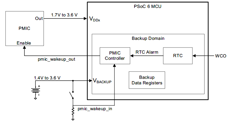
The backup domain is not a power mode but rather an always on group of resources that can be active during any of the device power modes.
A separate power supply provides power to a limited number of functions shown in Figure 12 while the main device power is removed. This results in the lowest power state possible while retaining a base level of functionality. The backup domain contains the pmic_wakeup_in pin allowing system-generated signals to trigger the repowering of the device and return to the CPU active power state.
A real time clock (RTC) allows periodic and accurate time-based wakeup triggers. By continuously powering the RTC using the VBACKUP supply accurate time can be maintained independently of the full device power state. Wakeup is accomplished by outputting a HIGH logic level on the pmic_wakeup_out pin most commonly used to enable an external power management integrated circuit (PMIC) supplying power to the full PSoC™ 6 MCU device.
64 bytes of SRAM storage are also maintained allowing key system state information to be retained when the device is repowered. The backup domain is powered by the VBACKUP supply that can be powered by a separate system supply, battery, or supercapacitor. In designs that do not require the backup domain to be powered separately from the rest of the PSoC™ 6 MCU device, VBACKUP should be connected directly to the VDDD supply.
VBackup supply
By providing a separate VBACKUP supply to the backup domain, the majority of the device may be completely powered down eliminating the leakage that would otherwise still occur in system hibernate power mode. If the backup domain is not powered separately from the rest of the device, VBACKUP and VDDD must be tied together.
The internal backup power supply named VDDBAK is automatically switched between VDDD and VBACKUP using an internal circuit. When VDDD is present and greater than 1.6 V, the VBACKUP supply is disabled in order to conserve battery or supercapacitor capacity. As VDDD drops below 1.6 V, the greater of VBACKUP or VDDD supplies is selected and the lower voltage supply connection is disabled. There are no sequencing restrictions between VBACKUP and VDDD. There is no need for external power supply isolation and switching circuits in most designs.
There are four common VBACKUP supply connection options.
VBACKUP directly connected to VDDD – When the backup domain is only used with the full PSoC™ 6 MCU device, there is no reason for a separate supply. VBACKUP and VDDD supply pins must be directly connected together as shown in Figure 13
Figure 13. Backup domain combined connection 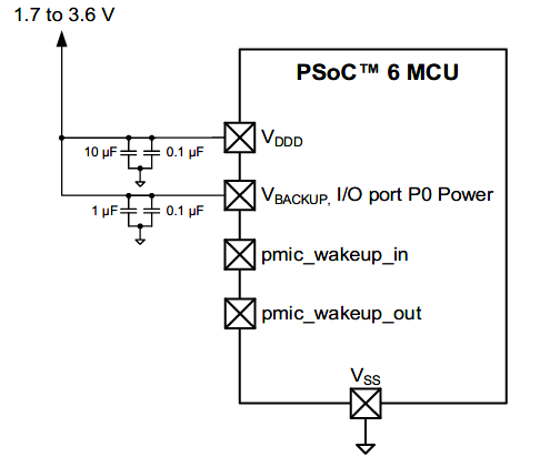
VBACKUP powered by supercapacitor – When a supercapacitor is used as the VBACKUP supply as shown in Figure 14, there are two options for recharging it. By calling the
Cy_SysPm_BackupSuperCapCharge()PDL function, the internal charge circuit is enabled any time the VDDD supply is selected as the active VDDBAK supplyThe key value of 0x3C must be passed in the function to avoid accidentally enabling the charge circuit. This charge circuit is not precise; the current varies in the range of 20 µA based on the difference between VDDD and VBACKUP. Recharge time is on the order of hours
The second option is to use an external charge circuit which can be optimized for any unique design challenges including a faster charge time. Both charge methods can be used in parallel. Any external charge components should be chosen to limit leakage current. The supercapacitor will be charged up to VDDD; therefore, ensure that it has an appropriate voltage rating
Figure 14. Backup domain supercapacitor connection Backup domain battery connection 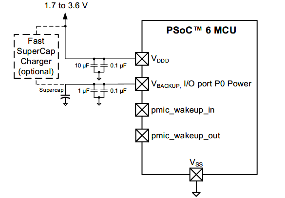
VBACKUP powered by battery – Figure 15 demonstrates a battery-powered VBACKUP . When a battery supplies VBACKUP, it is important to NOT use the supercapacitor charge circuit because it provides no battery safety mechanisms. If the battery is rechargeable, an external board-level recharge circuit can be provided for the battery-specific charge requirements
Figure 15. Backup domain battery connection 
- VBACKUP powered by system provided supply – If an always-on power supply is already present in the system, it can be used as the VBACKUP supply
On PSoC™ 6 MCU devices with up to 256 KB, 512 KB, 1 MB , or 2 MB of flash, one caution is that the Vmax supply switching logic requires VDDD to be powered up at least once for at least 50 µs after connecting the VBACKUP supply. This sets the switching circuitry in the correct state to isolate the VDDD supply from the VBACKUP supply by ensuring that there is no leakage path. No code execution is required. If not initialized, the VBACKUP domain will consume significantly more current from the battery and drain it prematurely. Increased leakage does not occur on PSoC™ 6 MCU devices with up to 256 KB of flash and on all newer PSoC™ 6 MCU devices. There are two cases where this leakage issue is likely to occur
- During manufacture of the PCB, the backup battery is installed and then the device is placed in storage in the high leakage state. Later, when the product is fully assembled, tested, and the PSoC™ 6 MCU device programmed, the logic state will be correctly set but the battery may have drained down during this period
- If the end product has a user-removable battery and VDDD is powered down, it is important that the PSoC™ 6 MCU be repowered after the user replaces the battery to reset the switch logic to its low-current state
The VBACKUP domain
does not contain a low-voltage detect circuit, so it is critical to not let the battery
or supercapacitor discharge below 1.4 V. If the VBACKUP supply browns out, a full device power cycle is
required to reenable the system. VBACKUP can be directly measured by the ADC by routing a 10%
scaled version through AMUXBUSA allowing the system to initiate a supercapacitor fast
recharge or notifying the user to change the battery. Measurement is enabled by calling
the Cy-SysPm_EnableBackupVMeasure() PDL driver
function.
VBACKUP also supplies all of the pins on Port0, so it is important to design their use for minimal current and leakage in your design while powered by the VBACKUP battery or a supercapacitor-based supply.
Backup domain reset
The backup domain is not reset by power-on reset (POR), brownout detect (BOD), watchdog timer (WDT), and external reset (XRES) events as long as VBACKUP or VDDD is present. The backup domain is reset only when both VBACKUP and VDDD are 0 V, or specifically reset through firmware. Under most circumstances, the backup domain should not be reset because it would cause the loss of the RTC time and any data stored in the backup data registers.
Backup domain reset is not required for POR, BOD, XRES, or system hibernate wakeups that occur while powered by the VDDD supply rail. Backup domain reset should occur only when power is removed from the VBACKUP supply or it is allowed to brownout.
The backup power domain is reset under firmware control by calling the
Cy_SysLib_ResetBackupDomain() PDL function. Firmware
must then confirm the BACKUP_RESET. RESET register field reads ‘0’ indicating that the
reset is completed prior to writing any backup domain registers due to the slower clock
rate of the backup domain logic circuits. After the backup domain is reset, the ILO must
also be disabled and reenabled to ensure that it is also reset.
Cy_SysClk_IloDisable() and
Cy_SysClk_IloEnable() PDL functions perform the ILO
reset. The init_cycfg_platform() function resets the
backup domain and ILO by default when using the initialization code supplied with ModusToolbox™-software.
The steps to reset the backup domain depend on the VBACKUP supply connection.
- VBACKUP directly connected to VDDD – If VBACKUP and VDDD are connected together, VBACKUP power is removed every power cycle, therefore the backup domain should be reset on all POR and BOD events. If the RTC and backup data registers are not used, it is safe to reset the backup domain after all reset events
- VBACKUP powered by a supercapacitor – If VBACKUP is connected to a supercapacitor, firmware should measure the supercapacitor voltage immediately after coming out of reset using the ADC. If the voltage on the supercapacitor is less than 1.4 V, it means the RTC and backup data cannot be trusted and firmware should reset the backup domain and allow time for the supercapacitor to recharge
- VBACKUP powered by battery – The battery voltage should be monitored periodically using the ADC. If it discharges near to its failure point, firmware should set a persistent flag in flash. After booting from reset, firmware can check the flag and know that the RTC and backup data cannot be trusted and the backup domain must be reset. When firmware detects that the battery voltage is good again, it can perform a final backup domain reset and then clear the flag
- VBACKUP powered by system-provided supply – The system should provide a method of informing the PSoC™ device firmware if the external VBACKUP supply was disabled, allowing firmware to reset the backup domain
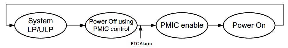
External PMIC control
The PSoC™ MCU backup domain provides power management IC (PMIC) control shown in Figure 16 to assist in powering up and down the main PSoC™ 6 MCU device supplies (VDDD, VDDA, VDDIO) provided by the PMIC. The pmic_wakeup_out pin is designed to connect directly to the PMIC device’s enable pin (active HIGH). The pmic_wakeup_out pin resets to a logic HIGH, ensuring that the PMIC and full PSoC™ 6 MCU device are initially powered. While fully powered, firmware can configure the pmic_wakeup_in pin or RTC wakeup sources and then power down the PMIC and therefore the main device. The PMIC is disabled by driving the pmic_wakeup_out pin LOW. When a HIGH logic level is applied to the pmic_wakeup_in pin or an RTC alarm occurs, the pmic_wakeup_out will be set HIGH, thereby reenabling the PMIC and repowering the main device.
To avoid errant code from disabling the PMIC controller, an unlock key is required before any other register writes. A value of 0x3A written to the BACKUP_PMIC_CTL.UNLOCK register disables the PMIC controller and allows the pmic_wakeup_out pin to be used as a GPIO. Any other value written to the UNLOCK field results in the PMIC controller being enabled.
Due to specific register write restrictions, you should use the SysPm PDL library which enforces the restrictions. See the device architecture TRM for full details on direct register access. Enabling the PMIC is a three-step process, which requires an unlock before any other register writes.
Cy_SysPm_PmicUnlock();
Cy_SysPm_PmicEnable();
Cy_SysPm_PmicLock();
The pmic_wakeup_out pin can be permanently set HIGH by executing
Cy_SysPm_PmicAlwaysEnable(). After calling this
function, the PMIC output cannot be disabled until VBACKUP
power is removed or the backup domain is reset.
Setting the pmic_wakeup_out pin LOW is accomplished by clearing the
BACKUP_PMIC_CTL.PMIC_EN register bit-field. Disabling the PMIC using PDL requires two
PDL instructions. The PMIC controller should not be relocked after disabling using PDL
because this will automatically re-enable the PMIC. The length of time from calling
Cy_SysPm_PmicDisable() until VDDD decays is dependent on the external
power supply design.
Cy_SysPm_PmicUnlock();
Cy_SysPm_PmicDisable();
There are many options other than a direct connection to a dedicated PMIC. This flexibility allows optimizing power switching to the needs of the design. Some of the common pmic_wakeup_out pin connections are as follows:
- Advanced PMIC device providing multiple supply rails to VDDD, VDDA, and VDDIO
- Simple LDO or switching regulator with enable pin supplying all PSoC 6 MCU device power pins
- Gate of low-leakage N-FET or equivalent switch allowing control of an existing regulated supply or a direct connection to a battery
- Digital signal to an external MCU or a controller managing the system power
Wakeup sources
The pmic_wakeup_in pin is the most flexible and lowest-current method of waking and repowering the PSoC™ 6 MCU because any circuit that can produce a HIGH logic level can be used. One of the most common methods is to connect the pin to a pull-down resistor and the user “power” button tied HIGH. If multiple wakeup sources are desired, a wired OR circuit can trigger the wake pin. The device can then optionally query the source of wakeup by using additional pins after power up. Figure 17 demonstrates a wired OR wakeup for detecting the press of the product’s power button or insertion of the USB cable.
The pmic_wakeup_in and hibernate_wakeup[1] signals share the same physical pin on Port0 and therefore have a restriction if both system hibernate and PMIC control are used in a design. The hibernate_wakeup[1] pin can wake the device on either a LOW or HIGH logic level that is set by its register configuration. The pmic_wakeup_in pin is active only with a HIGH logic level. If using both pin signals in the same design, ensure that a HIGH logic level is used to wake from hibernate and wake the PMIC. Another option is available on devices with a second hibernate_wakeup[0] pin, allowing the backup domain wakeup signals to be separated from hibernate wakeup on the second pin.
The RTC should be used for periodic wakeup of the full device if required because the WDT is not available in the backup domain. Use of the RTC requires a WCO be installed, thereby increasing the component count and current consumption. Wakeup using the RTC can be triggered at a specific alarm time using two separate alarms or every rollover of a periodic time based on day, hour, minute, or second. The RTC also allows external clock inputs from external sources like watch crystal oscillators and 50/60 Hz mains power. To aid in keeping an accurate time, a calibration register allows +/-1 ppm trim resolution of the WCO frequency. The RTC has specific data access restrictions; therefore, you should use the Cy_RTC PDL library which handles them properly. See the device architecture TRM for full details on direct register access to the RTC.
Backup data registers
The backup domain includes sixteen 32-bit registers, BACKUP_BREG[15:0], that retain their contents as long as the VBACKUP supply is valid. Each register holds 4 bytes of data for a total of 64 bytes. These registers are used to retain important system information and flags during power down of the full device. They can also be used during system hibernate mode allowing data to be read after device wake and reset.
Other power saving techniques
Use PSoC 6 MCU to gate current paths
Your PCB may contain other components that draw power; PSoC™ 6 MCUs can be used to control the power through them by supplying the power with GPIO pins that can be turned ON and OFF in firmware. Note that the maximum pin source and sink capabilities listed in the datasheet must not be exceeded. If a higher current is required than the GPIO can directly supply, use external power devices that are controlled by the GPIO.
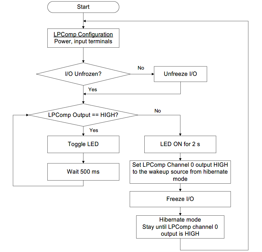
A good example of this scenario is a low-power comparator (LPComp) application as shown in Figure 18. In this case, the PSoC™ device compares the voltage on an analog pin, which changes as the potentiometer resistance changes.

LPComp can be turned OFF when not in use, but external components will still consume power because the current path through the resistor and potentiometer remains. A simple solution with PSoC™ 6 MCU is to use a second pin as a switch to ground, as shown in Figure 19.
In this configuration, the current flow can be stopped by writing a ‘1’ to Pin_3 and allowing the pin to float. This removes the current consumption by reducing the voltage differential across the two resistors to 0 V. Writing a ‘0’ resumes the current flow. Only one pin and a few lines of code are required to implement this power-saving feature.

Disable unused blocks
You can save unnecessary current consumption by disabling unused blocks. The power saved depends on the block disabled.
Use DMA to move data
You can save power any time you offload a task from the CPU and either halt the CPU or let it do something else in parallel. The DMA engine can be used in both system LP and ULP modes to transfer data with no CPU use. The power saved is either the difference between CPU active and CPU stop power modes if the CPU can be halted, or a lower CPU active current if the CPU can be clocked at a slower frequency and still get the same work done.
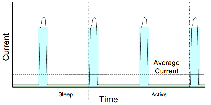
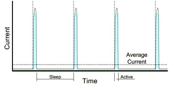
Periodic wakeup timers
A periodic wakeup from CPU sleep mode is the most common way to reduce power consumption. The average power consumption is determined by the ratio of CPU active period power consumption and CPU sleep period power consumption. To achieve the best result, the sleep period should be as long as possible and the active period should be as short as possible. An example of CPU sleep mode power savings from the CY8C61x6 datasheet is CM4 active = 1.7 mA (SIDF5) and CM4 sleep = 0.76 mA (SIDS7).
The WDT and multi-counter WDT (MCWDT) are effective periodic wakeup sources in system deep sleep and system hibernate modes. If your application needs longer, or more precise wakeup periods, an RTC alarm can be a good periodic wakeup source. See CE237278 - HAL: RTC alarm periodic wakeup for a code example using the RTC periodic timer for wakeup. An example of system deep sleep mode power savings from the CY8C61x6 datasheet is CM4 active = 1.7 mA (SIDF5) and system deep sleep = 7 µA (SIDDS1).
The following scenarios show how to change the mode states:
- System hibernate
- System deep sleep
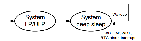
- Power OFF with an external PMIC
Disabling CPUs
If the CM4 CPU is not used in the application, disable it by calling the
Cy_SysDisableCM4() function from the CM0+ firmware. You
can also set the Clk_Fast divider to 256 to minimize any fan-out leakage from this
clock.
Splitting tasks between the CPUs
There are several reasons to choose either CM4 or CM0+ to do certain tasks. For example:
- Tasks that require floating point or DSP operations are more efficiently run on CM4
- Tasks that are time-critical requiring the maximum clock speed (150 MHz) should run only on CM4
- If deterministic timing is required by a single task independent of all other tasks, it is often beneficial to move that task to its own CPU to simplify timing. Usually, the CM0+ CPU is used for this purpose
- When maximizing the system idle state time as discussed in Clocks, it may be beneficial to spread tasks between CM0+ and CM4 so that the lower-power idle state can be entered faster due to simultaneous task processing
- If single CPU processing must be spread out over a long period due to real-time hardware interactions that limit time spent in lower-power states, CM0+ will often be lower-power than CM4 over the same active time interval
- If processing power is required that exceeds what one CPU can provide, the tasks should be spread between both cores. Because each core has its own bus controller and can access separate memory blocks, there are minimal wait states due to bus or memory contention. The performance decrease due to contention is typically less than 2% while the performance increase from the second core is greater than 50% (assuming CM0+ added to CM4)
- In applications that stay in active mode and can achieve the required processing power on a single core, there is most often no power benefit to sharing the required tasks between cores
Clocks
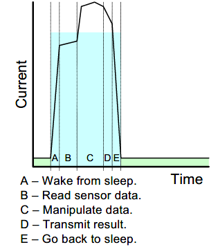
In some cases, running CPU clocks faster can result in a lower average current consumption. For example, consider a design that takes a reading from a sensor once every second, performs several calculations, and then transmits the results to another device.
You can use CPU sleep or system deep sleep mode to reduce power when the PSoC™ device is idle, but the average current consumption can be higher because of the additional time spent in CPU active mode. Figure 20 is a representation of the current consumption of this example with the system clocks set at 8 MHz.
Depending on the tasks or calculations that are being performed when the PSoC™ device is awake, it may be possible to complete them sooner by running the CPU clocks faster. This can reduce the average current consumption because the PSoC™ device is in CPU active mode for less time and in CPU sleep or system deep sleep longer. Figure 21 is a representation of CPU active mode timing, broken up into tasks.
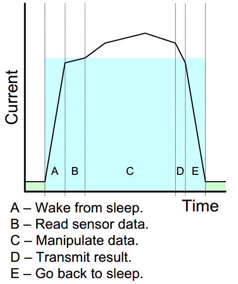
The time required for some tasks does not change even if the system clock frequency increases. Sensor reading and data transmitting fall into this category. Other tasks like data processing, require less time if the CPU operates at a faster frequency.
At some point, the benefit of a shorter active time is overcome by the energy required to drive the clocks at a higher rate. Assume that the optimal speed is 48 MHz, as Figure 22 shows. With a 48 MHz clock, the time spent in active mode is about half the time spent with an 8 MHz clock. Figure 22 shows that the peak current consumption is greater when the clocks are faster, but the overall average is lower due to the longer time spent in CPU sleep or system deep sleep. On PSoC™ 6 MCU devices, it is generally better to run the CPU as fast as possible to complete processing and spend more time in the low-power mode.
GPIOs
GPIOs can continue to drive external circuitry while the PSoC™ device is in any low-power mode. This is helpful when you need to hold external logic at a fixed level, but it can lead to wasted power if the pins needlessly source or sink current. The specific power savings of this technique depend on the circuit attached to the specific GPIO pin.
You should analyze your design and determine the best state for your GPIOs
during low-power operation. If holding a digital output pin at logic ‘1’ or ‘0’ results
in the lowest current, match that digital level using
cyhal_gpio_write().
/* Set MYPIN_0_NUM to ‘0’ for low power using HAL APIs.*/
cyhal_gpio_write(MYPIN_0_NUM, 0u);
Configure all unused GPIOs to Analog High-Z unless there is a specific reason
to use a different drive mode. The High-Z drive mode results in the lowest current for a
GPIO pin. A pin’s drive mode may be set using the
cyhal_gpio_configure() HAL function.
/* Set MYPIN_0_NUM to Analog HI-Z for low power using HAL APIs. */
cyhal_gpio_configure(P0_0, CYHAL_GPIO_DIR_INPUT, CYHAL_GPIO_DRIVE_NONE);
Cy_SysPm_IoUnfreeze() after configuring the GPIO pins
and setting their output drive state. See CE231030 - PSoC™ 6 MCU: Wakeup from
hibernate using a low-power comparator for a code example on
hibernate and I/O control.SRAM
PSoC™ 6 MCU devices allow powering off individual SRAM banks or pages within a bank. The size of pages within a bank depends on the specific device and bank as detailed in the device datasheet. Specific devices will have one or more SRAM banks. Most devices have one bank with a smaller page size (typically 32 KB) for fine-grained control of the amount of SRAM enabled. Any unused page can be disabled by writing to the CPUSS power control registers. This technique is most useful in system deep sleep mode where retaining 64 K SRAM = 7 µA (SIDDS1) while retaining 256 K SRAM = 9 µA (SIDDS2) as listed in the CY8C61x6 datasheet.
/* Power off all except the first two pages of RAM0 */
for (uint32_t i = 2; i < NUM_RAM_PAGES; i++)
   {
      CPUSS->RAM0_PWR_MACRO_CTL[i] = 0x05FA0000;
   }
/* Additional SRAM banks */
CPUSS->RAM1_PWR_CTL = 0x05FA0000;
CPUSS->RAM2_PWR_CTL = 0x05FA0000;
Consult the register TRM of the device for all power control registers.
As an advanced use case, modification of the project’s linker script can be used with SRAM power down to optimize the total amount of SRAM required or allow custom data placement in support of dynamic SRAM powering.
TCPWM
When using a counter, timer or PWM, you should configure the clock sourcing the channel as low as possible while still meeting your frequency and accuracy requirements. For example, if you need to generate a 1-second interrupt with a timer, it is better to use a clock frequency of 1 kHz with the period equaling 1,000 counts than a clock frequency of 1 MHz with a period equal to 1,000,000 counts. The power savings from reducing the TCPWM clock is mostly linear based on clock frequency. TCPWM operating current at 100 MHz = 540 µA (SID.TCPWM.2B) while at 8 MHz = 70 µA (SID.TCPWM.1) per the CY8C61x6 datasheet.
The same idea applies when using a PWM to dim an LED. Use the minimum clock frequency possible that does not let the human eye perceive that the LED is blinking. 60 Hz is a good frequency for most applications. Figure 24 shows a comparison between the clock settings for the TCPWM block.
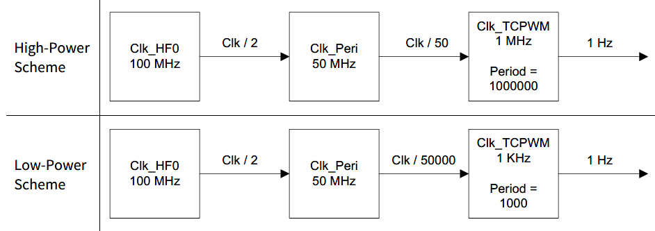
The TCPWM block has a clock prescaler feature. For minimum power consumption, maximize the peripheral clock divider first before using the TCPWM clock prescaler.
If the TCPWM block uses any pin connections, set the pins to Analog High-Z when the block is disabled. If the PSoC™ device supports digital system interconnect (DSI), avoid using DSI by choosing the TCPWM channels with direct connection to the desired pin assignment. If the PSoC™ device supports UDBs (universal digital block), use all fixed-function TCPWM channels first instead of UDB-based TCPWMs.
SCB
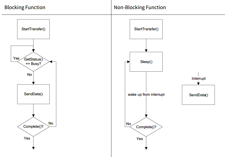
Avoid using blocking functions when sending or receiving data. Use interrupt-based events or an RTOS to transfer the data while yielding the CPU to other tasks. The idea behind this strategy is to keep the CPU in a sleep state longer, instead of polling the status of the transmission. Figure 25 shows an example of blocking and non-blocking functions.
Instead of using the SCB interrupt to access its FIFO in firmware, use DMAs controlled by the FIFO level to reduce the amount of CPU cycles required in the application; therefore, the CPU can stay in a sleep state longer or execute other tasks.
If the SCB block uses any pin connections, set the pins to Analog High-Z when the block is disabled. If the PSoC™ device supports DSI, avoid using it by choosing SCB channels with direct connections to the desired pin assignment. If the PSoC™ device supports UDBs, use all fixed-function SCB channels before using UDB-based communication interfaces.
Operating at the lowest data rate the system can support also helps in reducing power because the SCB’s power increases linearly with clock frequency. For example, running I2C at 1 Mbps = 180 µA (SID152) while running at 100 kbps = 30 µA (SID149) as shown in the CY8C61x6 datasheet.
Audio subsystem
The I2S and PDM/PCM blocks are generally sourced by a high-frequency clock generated from the PLL. For high-accuracy frame rates, an ECO sources the PLL. When picking a frequency for the ECO, consider what the desired audio sample rates are:
- To support all standard audio sample rates (8/16/22.05/32/44.1/48 kHz), the minimum ECO frequency you can use is 17.2032 MHz
- To support only the sample rates 8/16/48 kHz, configure the PLL for 12.288 MHz
- To support only the sample rates 22.05/44.1 kHz, configure the PLL for 22.5792 MHz
If the Audio Subsystem is not in use disable the I2S and/or PDM/PCM blocks. You must also disable the PLL and ECO, which are the main reasons for high current consumption.
If the accuracy of the frame rates is not important for the application, do not use the ECO and/or PLL. For example, if your application implements a sound detector and can tolerate a higher error, use the FLL as the source for the audio subsystem. Once a sound is detected and the system needs to be fully operational, enable the PLL and ECO to sample at a higher accuracy.
Instead of using audio subsystem interrupts to access its FIFO in firmware, use DMAs controlled by the FIFO level triggers to reduce the number of CPU cycles required in the application so that the CPU can stay in a sleep state longer or execute other tasks.
USB
When there is no activity on the USB bus, you can suspend the USB block to consume less current. See the code example CE223305 – PSoC™ 6 MCU: USB suspend and resume to learn how to set up the device to enter and exit low-power states.
Low-power comparator
If the low-power comparator requires pin connections and system deep sleep operation, always choose the dedicated pin connections to the comparator. This allows the comparator to work in system deep sleep and avoid using the global analog muxes, which consume additional current to stay active.
There are two ways to verify the status of the comparator: Call the
cyhal_comp_read() function, or set up an interrupt. In
most cases, it is preferred to use the interrupt method, which reduces the CPU
usage.
The comparator supports three operation modes that affect its speed and power:
- Ultra-low-power/Slow: ICMP1 = 0.85 µA (SID259) – Slows the response time to 20 µs (SID92). Use this mode when in system deep sleep or hibernate only
- Low-power/Low: ICMP2 = 10 µA (SID248) – Preferred mode when system deep sleep or hibernate are not required and the slower response time of 1 µs (SID258) is acceptable. This increases the input offset voltage to 25 mV (SID85A)
- Normal Power/Fast: ICMP1 = 150 µA (SID89) – Use it when the fastest response time of 100 ns (SID91) and/or a low offset voltage of 10 mV (SID84) are required
Another option to reduce the amount of current consumed by the comparator is to disable hysteresis. Hysteresis can be disabled in the device configurator tool of ModusToolbox™.
SAR ADC
When selecting the pins to be connected to the SAR ADC, preferably choose the dedicated port connected to the SAR MUX first. Only after running out of pins in that port, choose pins from other ports. By only using the dedicated port, there is no need to use the global analog muxes, which consume extra current. You can also achieve higher sample rates with the dedicated port due to lower input capacitance.
If the full-rated accuracy of ADC results is not required, use a lower resolution and do not use averaging, which reduces the number of ADC clocks required for the same sample rate.
If the maximum sample rate is not required, consider using the single-shot mode instead of continuous mode. This avoids the SAR ADC operating all the time. In single shot mode, the ADC samples only when triggered by software or hardware, depending on the application.
If the main application is not required to perform processing during ADC sampling, the CY8C62x4 family of devices support SAR ADC operation in system deep sleep power mode. See AN230938 – PSoC™ 6 MCU low-power analog for details of the low-power analog features of the CY8C62x4 family.
Voltage DAC
If the DAC voltage output needs to be periodically changed with pre-determined values, use a DMA to update the voltage value. This avoids using CPU cycles to write to DAC registers.
If the external device that requires the DAC output voltage is used only periodically, keep the DAC disabled when its output is not required.
When the DAC output voltage must be provided while in system deep sleep, use a “sample-and-hold” strategy to maintain the voltage output while the voltage DAC is disabled in system deep sleep. See the code example CE220925 – PSoC™ 6 MCU VDAC sample and hold for more details. The DAC operating current = 125 µA (SID100D) while the DAC current stopped = 1 µA (SID101D) per the CY8C61x6 datasheet.
Opamp
The opamp supports three different operating modes – Low, Medium, and High. These operation modes are affected by the system power modes – system LP/ULP and deep sleep. In system deep sleep, there are two additional modes to choose from. Table 4 shows how to choose the appropriate operation mode.
| Specification | High-power operation mode | Medium-power operation mode | Low-power operation mode | |||
|---|---|---|---|---|---|---|
| LP/ULP | Deep sleep | LP/ULP | Deep sleep | LP/ULP | Deep sleep | |
Minimum gain-bandwidth | 6 MHz | M1: 4 MHz M2: 0.5 MHz | 4 MHz | M1: 2 MHz M2: 0.2 MHz | 1 MHz | M1: 0.5 MHz M2: 0.1 MHz |
Maximum output current (no load) | 1500 µA | M1: 1500 µA M2: 120 µA | 600 µA | M1: 600 µA M2: 60 µA | 350 µA | M1: 350 µA M2: 15 µA |
Response time | 150 ns | 400 ns | 2000 ns | |||
M1: Mode 1 has higher GBW and highest current.
M2: Mode 2 has a lower GBW and the lowest current. When selecting the pins to be connected to the opamp, preferably choose the dedicated pins connected to the opamp. By using only the dedicated pins, there is no need to use the global analog muxes, which consume extra current.
Power measurement
Measuring the current with a DMM
When using a digital multimeter (DMM) to measure device current, it is important to know the value of the shunt resistor in the DMM. DMMs have one or more (shunt) resistors between the current inputs. These resistors can range from less than an ohm to more than 10 kΩ. There is no standard value for the shunt resistor between brands or even models from the same vendor. It is important to review your meter’s manual and learn the value of the shunt resistor because there will always be a voltage drop across this shunt. This means that the PSoC™ device will not see the same voltage you think you are supplying. If the shunt resistor in your meter is 1 Ω or less, you will see only a few millivolts of drop when measuring PSoC™ MCU current, which can be ignored. If the shunt resistor is 1 kΩ, which some vendors use for low-current measurements, a 1 mA current will result in a drop of 1 V.
High shunt resistor values can cause the device to reset due to low voltage at higher currents. Also, when changing ranges, be careful that the DMM does not do a “break-before-make”, or the power will be cycled and your project will be reset.
For extremely low currents in deep sleep, hibernate, and stop modes, a good technique is to use a zero or low- resistance shunt until the device enters low-power mode. After entering low-power mode, the code should keep the device in that mode and switch to a high-resistance shunt for current measurement.
As an alternative to relying on the DMM shunt, most PSoC™ 6 MCU kits include a place for a shunt resistor or current measurement header. See the respective kits user guide to determine specific current measurement features. These can be replaced or connected to a small resistor allowing measurement of the voltage across the shunt with a voltmeter. You can then easily determine the current. A shunt between 1 Ω and 100 Ω should work well for most applications.
Approximating the power consumption
The device datasheet provides information to estimate PSoC™ 6 MCU power consumption for project-specific user configurations. To simplify this process, a spreadsheet has been provided that includes typical power requirements for a wide range of internal components and modes. The spreadsheet includes CY8C62x4 devices which contain low-power analog peripherals detailed in AN230938 – PSoC™ 6 MCU low-power analog. This spreadsheet , PSoC™ 6 Power Calculator (version 3) - AN219528.xlsx, is located on the Documents section of 32-bit PSoC™ 6 Arm® Cortex®-M4 / M0+ web page. Because every project is different, the power calculation provided by this spreadsheet is only an estimate of typical values but should be close enough to provide feedback before your design is complete.
There are several tabs in the spreadsheet; make sure that you read the “Instructions” tab before entering your data. Five “Config” tabs allow configuration of different hardware settings and power modes that the device can transition through at run time. The “Summary” tab displays the current for each configuration as well as the peak and average current across all modes based on the time spent in each configuration. An optional battery life estimation section on the “Summary” tab estimates battery life based on the average current.
Power supply protection system
Hardware control
Brownout detect (BOD)
Brownout detect (BOD) can reset the system before the logic state is lost when VDDD and VCCD power are lost. The brownout system guarantees a reset before VDDD reaches the minimum system operating voltage, and works for all logic, SRAM, and flash. BOD is controlled by hardware; there is no configurable register.
Low-voltage detect (LVD)
Low-voltage detect (LVD) is similar to BOD but its threshold voltage is configurable. LVD generates an interrupt when VDDD falls under a configured trip voltage. This interrupt allows the application time to handle important data before the BOD reset is triggered. LVD provides 15 selectable trip voltages. LVD is not available in system deep sleep and hibernate modes.
Overvoltage detect (OVD)
Overvoltage detect (OVD) is the opposite of BOD. These circuits generate a reset when unsafe overvoltage supply conditions on VDDD and VCCD are detected. No firmware control is required. OVD helps to protect the system from high-voltage damage.
Summary
Many power managing options can be used in PSoC™ 6 MCU. By following proper methods, you can optimize your design and ensure that the power modes and features of PSoC™ 6 MCU give the best options for the lowest power consumption without degrading the required performance of battery powered devices.
Power modes summary
Power modes and wakeup source
| System power mode | MCU power mode | Description | Entry conditions | Wakeup sources | Wakeup action |
|---|---|---|---|---|---|
| LP | Active | Primary mode of operation. 1.1 V core voltage. All peripherals are available (programmable). Clocks at their maximum frequencies. |
| Not applicable | N/A |
| Sleep | 1.1 V core voltage. One or more CPUs in sleep mode (execution halted). All peripherals are available (programmable). Clocks at their maximum frequencies. | In system LP mode, the CPU executes the WFI/WFE instruction with deep sleep disabled | Any interrupt to CPU | Interrupt | |
| Deep sleep | 1.1 V core voltage. One CPU in deep sleep mode (execution halted). Other CPU in active or sleep mode. All peripherals are available (programmable). Clocks at their maximum frequencies. | In system LP mode, the CPU executes the WFI/WFE instruction with deep sleep enabled | Any interrupt to CPU | Interrupt | |
| ULP | Active | 0.9 V core voltage. All peripherals are available (programmable). Clock frequencies are limited. | Manual register write from system LP mode. Wakeup from CPU sleep or CPU deep sleep while in system ULP mode. Wakeup from system deep sleep after entered from ULP mode. | Not applicable | N/A |
| Sleep | 0.9 V core voltage. One or more CPUs in sleep mode (execution halted). All peripherals are available (programmable). Clock frequencies are limited. | In system ULP mode, the CPU executes the WFI/WFE instruction with deep sleep disabled | Any interrupt to CPU | Interrupt | |
| Deep sleep | 0.9 V core voltage. One CPU in deep sleep mode (execution halted). Other CPU in active or sleep mode. All peripherals are available (programmable). Clock frequencies are limited. | In system ULP mode, the CPU executes the WFI/WFE instruction with deep sleep enabled | Any interrupt to CPU | Interrupt | |
| Deep sleep | Deep sleep | All high-frequency clocks and peripherals are turned off. Low-frequency clock (32 kHz) and low-power analog and digital peripherals are available for operation and as wakeup sources. SRAM is retained (programmable). | Both CPUs simultaneously in CPU deep sleep mode | GPIO interrupt, low-power comparator, SCB, CTBm, watchdog timer, and RTC alarms | Interrupt |
| Hibernate | N/A | GPIO states are frozen. All peripherals and clocks in the device are completely turned OFF except the low-power comparator and backup domain. Wakeup is possible through WAKEUP pins, XRES, low-power comparator (programmable), and RTC alarms (programmable). Device resets on wakeup. | Manual register write from LP or ULP modes | WAKEUP pin, low-power comparator, watchdog timer1, and RTC2 alarms. | Reset |
Subsystem availability
Resources available in different power modes
Table 6 shows information for the resource availability in different power modes.
| Component | System power modes | |||||||
|---|---|---|---|---|---|---|---|---|
| LP | ULP | Deep sleep | Hibernate | XRES | Power off with backup | |||
| CPU active | CPU sleep/deep sleep | CPU active | CPU sleep/deep sleep | |||||
| Core functions | ||||||||
| CPU | On | Sleep | On | Sleep | Retention | Off | Off | Off |
| SRAM | On | On | On | On | Retention | Off | Off | Off |
| Flash | Read/Write | Read/Write | Read only | Read only | Off | Off | Off | Off |
| High-speed clock (IMO, ECO, PLL, FLL) | On | On | On | On | Off | Off | Off | Off |
| LVD | On | On | On | On | Off | Off | Off | Off |
| ILO | On | On | On | On | On | On | Off | Off |
| Peripherals | ||||||||
| SMIF | On | On | On | On | Retention | Off | Off | Off |
| UDB | On | On | On | On | Off | Off | Off | Off |
| SAR ADC | On | On | On | On | Off | Off | Off | Off |
| CTBm | On | On | On | On | On (lower GBW) | Off | Off | Off |
| LPCMP | On | On | On | On | On3 | On4 | Off | Off |
| TCPWM | On | On | On | On | Off | Off | Off | Off |
| CSD | On | On | On | On | Retention | Off | Off | Off |
| Bluetooth LE | On | On | On | On | Retention | Off | Off | Off |
| LCD | On | On | On | On | On | Off | Off | Off |
| SCB | On | On | On | On | Retention (I2C/SPI wakeup available)5 | Off | Off | Off |
| GPIO | On | On | On | On | On | Freeze | Off | Off |
| Watchdog timer | On | On | On | On | On | On | Off | Off |
| Multi-counter WDT | On | On | On | On | On | Off | Off | Off |
| Resets | ||||||||
| XRES | On | On | On | On | On | On | On | Off |
| POR | On | On | On | On | On | On | Off | Off |
| BOD | On | On | On | On | On | Off | Off | Off |
| Watchdog reset | On | On | On | On | On | On6 | Off | Off |
| Backup domain | ||||||||
| WCO, RTC, alarms | On | On | On | On | On | On | On | On |
Callback function examples
Register callback functions using HAL
cyhal_syspm_callback_data_t callback_data_sleep =
    {
        .callback = syspm_app_callback,
        .states = (cyhal_syspm_callback_state_t)(CYHAL_SYSPM_CB_CPU_SLEEP | CYHAL_SYSPM_CB_SYSTEM_LOW),
		.ignore_modes = (CYHAL_SYSPM_CHECK_READY | CYHAL_SYSPM_CHECK_FAIL),
        .args = NULL,
        .next = NULL,
    };

    cyhal_syspm_callback_data_t callback_data_hibernate =
    {
        .callback = syspm_app_callback,
        .states = (cyhal_syspm_callback_state_t)(CYHAL_SYSPM_CB_SYSTEM_HIBERNATE | CYHAL_SYSPM_CB_SYSTEM_LOW),
        .args = NULL,
        .next = NULL,
    };

	cyhal_syspm_register_callback(&callback_data_sleep);
    cyhal_syspm_register_callback(&callback_data_hibernate);
Implement custom callback functions using HAL
bool syspm_app_callback(cyhal_syspm_callback_state_t state, cyhal_syspm_callback_mode_t mode, void *callback_arg)
{
    (void)callback_arg;
    bool allow_transition = true;

    switch (mode)
    {
        case CYHAL_SYSPM_CHECK_READY:
            /* Check to see if it is OK to change power modes. */
            /* If it is OK the change, make sure nothing will invalidate this and return true. */
            /* If it is not OK the change, return false. */
            /* Example: prevent transition if requested mode is HIBERNATE. */
            allow_transition = (state != CYHAL_SYSPM_CB_SYSTEM_HIBERNATE);
            break;
        case CYHAL_SYSPM_CHECK_FAIL:
            /* Undo anything done as part of CHECK_READY since it is not actually chaning. */
            break;
        case CYHAL_SYSPM_BEFORE_TRANSITION:
            /* Do anything necessary to shut things down. */
            break;
        case CYHAL_SYSPM_AFTER_TRANSITION:
            /* Undo anything done as part of CHECK_READY or BEFORE_TRANSITION since it is coming back up. */
            break;
    }

    return allow_transition;
}
Code examples
CE219881 - PSoC 6 MCU: Switching between power modes
This code example shows how to enter and exit system LP and ULP power modes and transition the CPU from CPU active to sleep or deep sleep. Once in either mode, the example also shows how to wake up and return to one of the system LP or ULP modes and CPU active mode.
The project uses a switch to transition among power modes and shows different LED colors to indicate the current power mode. Figure 26 shows the state machine implemented in the firmware to execute the transitions. For more information, see CE219881 - PSoC™ 6 MCU: Switching between power modes.
CE231030 - PSoC 6 MCU: Wakeup from hibernate using a low-power comparator
This code example demonstrates how to set the Component options for the LPComp internal reference voltage and how to set the external input from a GPIO using the LPComp driver. The project is a good example of the system hibernate power mode transition. It teaches you how to handle the GPIOs before and after system hibernate, and it shows how to register the wakeup source for hibernate. Figure 27 shows the basic flow of the project. For more information, see CE231030 - PSoC™ 6 MCU: wakeup from hibernate using a low-power comparator.
CE237278 - HAL: RTC alarm periodic wakeup
This code example shows how to enter DeepSleep and Hibernate modes, as well as how to use RTC to generate an RTC alarm to wake up the MCU from DeepSleep and Hibernate modes.
The MCU enters either DeepSleep or Hibernate mode based on the duration that the user button is pressed. The RTC alarm wakes up the system and prints the wakeup information to the UART terminal. For more information, see CE237278 - HAL: RTC alarm periodic wakeup.

CE226306 - PSoC 6 MCU power measurements
This example shows how to configure PSoC™ 6
MCU devices to run the clock frequencies and system modes specified in the device-level
specifications table in PSoC™ 6 MCU datasheets. After
building and programming the application into PSoC™ 6
MCU devices, you can measure the current the PSoC™ 6
MCU device consumes and compare it against the values specified in the datasheet. You
can select the power configuration by changing a #define in
firmware.
| Configuration | Options | Description |
|---|---|---|
System mode | SYSTEM_LP SYSTEM_ULP | Defines the system mode the firmware enters – system low-power or system ultra-low-power modes. The following functions are used: |
Core voltage supply | VCCD_1V1 VCCD_0V9 | Defines the core voltage supply for the BUCK or LDO – 0.9 V or 1.1 V. |
Cache support | RUN_FROM_FLASH RUN_FROM_CACHE | Defines if cache is used. If cache is disabled, the following instructions are used: The
|
CM4 CPU mode | CM4_WHILE_LOOP CM4_DHRYSTONE CM4_SLEEP CM4_DEEP_SLEEP | Defines what the CM4 CPU runs – While (1) loop, Dhrystone algorithm, go to CPU sleep, or go to CPU deep sleep. The following functions are used: while (1); // Runs a forever while loop dhrystone(); //
Runs the Dhrystone instructions
Cy_SysPm_CpuEnterSleep(CY_SYSPM_WAIT_FOR_INTERRUPT); // Sleep
Cy_SysPm_CpuEnterDeepSleep(CY_SYSPM_WAIT_FOR_INTERRUPT); //
Deep-Sleep |
CM4 CPU frequency [CM4_FREQ_MHZ] | FREQ_8_MHZ FREQ_25_MHZ FREQ_50_MHZ FREQ_100_MHZ | Defines the clock frequency for HFCLK0, which is linked to the CM4 CPU clock. The following functions are used: |
CM0+ CPU mode | CM0P_WHILE_LOOP CM0P_DHRYSTONE CM0P_SLEEP CM0P_DEEP_SLEEP CM0P_HIBERNATE | Defines what the CM0+ CPU runs – While (1) loop, Dhrystone algorithm, go to CPU sleep, go to CPU deep sleep or hibernate The same functions from the CM4 CPU Mode are used. Cy_SysPm_SystemEnterHibernate(); // Go to Hibernate |
CM0+ CPU frequency [CM0P_FREQ_MHZ] | FREQ_8_MHZ FREQ_25_MHZ FREQ_50_MHZ FREQ_100_MHZ | Defines the clock frequency for the CM0+ CPU clock. The following function is used: |
Clock source | USE_IMO USE_FLL | Defines the clock source for the HCLK0 – IMO or FLL. If IMO is used, the FLL is bypassed. If the FLL is used, the IMO is still used as the source for the FLL. The following functions are used: |
Minimum regulator current mode | MIN_CURRENT | Determines whether the firmware calls the
|
References
Application notes
Code examples
Revision history
Document version | Date of release | Description of changes |
|---|---|---|
** | 2017-09-12 | New application note. |
*A | 2018-05-05 | Updated power mode names to match TRM names; CPU active, CPU, sleep, CPU deep sleep, system LP, system ULP, system deep sleep, system hibernate. |
*B | 2019-12-19 |
|
*C | 2020-11-23 | Complete rewrite of Chapter 3.3 Backup Power Domain to add more details on its operation. |
*D | 2021-07-29 | Added reference to AN230938 – PSoC™ 6 MCU low-power analog and added its content to the PSoC_6_Power_Estimator.xlsx power estimation spreadsheet. |
| *E | 2022-07-21 | Template update |
| *F | 2023-01-23 | No content change; added the "PSoC™ 6 Power Calculator (version 2).xlsx" file in the source of DMS. |
| *G | 2023-03-28 |
|
Trademarks
The Bluetooth® word mark and logos are registered trademarks owned by Bluetooth SIG, Inc., and any use of such marks by Infineon is under license. PSOC™, formerly known as PSoC™, is a trademark of Infineon Technologies. Any references to PSoC™ in this document or others shall be deemed to refer to PSOC™.