AN85951 PSOC™ 4 and PSOC™ 6 MCU CAPSENSE™ design guide
About this document
Scope and purpose
The CAPSENSE™ design guide explains how to design capacitive touch sensing applications with the CAPSENSE™ feature in PSOC™ 4 and PSOC™ 6 MCU device families. The CAPSENSE™ feature offers unprecedented signal-to-noise ratio (SNR), best-in-class liquid tolerance, and a wide variety of sensors such as buttons, sliders, touchpads, and proximity sensors. This design guide explains the CAPSENSE™ operation, CAPSENSE™ design tools, performance tuning of the PSOC™ Creator and ModusToolbox™ CAPSENSE™ component and design considerations. This guide also introduces Fifth Generation CAPSENSE™ technology which has several advantages over the previous generation devices.
Different device families are available with CAPSENSE™ feature. If you have not chosen a particular device, or are new to capacitive sensing, see the
Getting started with CAPSENSE™ design guide
. It helps you understand the advantages of CAPSENSE™ over mechanical buttons, CAPSENSE™ technology fundamentals, and to select the right device for your application. It also directs you to the right documentation, kits, or tools to help with your design.
Intended audience
This document is primarily intended for engineers who need to become familiar with the CAPSENSE™ design principles of PSOC™ 4 and PSOC™ 6 MCU devices.
Introduction
Overview
Capacitive touch sensors are user interface devices that use human body capacitance to detect the presence of a finger on or near a sensor. CAPSENSE™ solutions bring elegant, reliable, and easy-to-use capacitive touch sensing functionality to your product.
This design guide focuses on the CAPSENSE™ feature in the PSOC™ 4 and PSOC™ 6 MCU families of devices. These are true programmable embedded system-on-chip, integrating configurable analog and digital peripheral functions, memory, radio, and a microcontroller on a single chip. These devices are highly flexible and can implement many functions such as ADC, DAC, and Bluetooth® LE in addition to CAPSENSE™, which accelerates time-to-market, integrates critical system functions, and reduces overall system cost.
This guide assumes that you are familiar with developing applications for PSOC™ 4 and PSOC™ 6 MCU using the PSOC™ Creator integrated design environment (IDE). If you are new to PSOC™ 4, see AN79953 - Getting started with PSOC™ 4 or AN91267 - Getting started with PSOC™ 4 Bluetooth® LE . If you are new to PSOC™ 6 MCU, see AN221774 – Getting started with PSOC™ 6 MCU and AN210781 - Getting started with PSOC™ 6 MCU with Bluetooth® LE connectivity . If you are new to PSOC™ Creator, see the
PSOC™ Creator home page
.
If you are new to ModusToolbox™, see
ModusToolbox™ IDE quick start guide
.
This design guide helps you understand:
- CAPSENSE™ technology in PSOC™ 4 and PSOC™ 6 MCU
- Design and development tools available for PSOC™ 4 and PSOC™ 6 MCU PSOC™ 6 MCU CAPSENSE™
- PSOC™ 6 MCU CAPSENSE™ PCB layout guidelines for PSOC™ 4 and PSOC™ 6 MCU
- Performance tuning of PSOC™ 4 and PSOC™ 6 MCU CAPSENSE™ component
Applications using CAPSENSE™ Plus features such as motor control systems and induction cookers
CAPSENSE™ features
CAPSENSE™ in PSOC™ 4 and PSOC™ 6 MCU has the following features:
Supports self-capacitance (CSD) and mutual-capacitance (CSX) based touch sensing on all CAPSENSE™-capable GPIO pins 1
Provides the best-in-class signal-to-noise ratio (SNR), allowing high sensitivity that provides high-range proximity sensing (up to a 30-cm proximity-sensing distance) and liquid-tolerant operation (see Liquid tolerance )
High-performance sensing across a variety of overlay materials and varied thickness (see CAPSENSE™ fundamentals , Overlay material , and Overlay thickness )
SmartSense auto-tuning technology
Pseudo random sequence (PRS) clock source, supports spread spectrum and programmable resistance switches for lower electromagnetic interference (EMI)
Low power consumption with as low as 1.71-V operation and as low as 150-nA current consumption in Hibernate mode
The PSOC™ 4100S Max device introduces the fifth-generation CAPSENSE™ technology (
Ratiometric sensing technology
) and has the following additional features when compared to older generations:
Improved SNR : Fifth-generation CAPSENSE™ technology ( Ratiometric sensing technology ) significantly improves noise performance compared to previous generation devices
Improved refresh rate : The better sensitivity of multi sense converter (MSC) requires less time to get a similar signal as in previous generations; therefore, it is able to achieve a higher refresh rate. The two independent MSC blocks, which can scan the sensors in parallel improve the refresh rate further especially in use cases where large numbers of sensors need to be scanned
Improved CPU bandwidth : Scan supported in both CPU mode and DMA mode. The CPU mode is a conventional interrupt-driven mode, while the DMA mode is capable of autonomous scanning which reduces the CPU bandwidth requirement to 18% compared to previous generations
Improved noise immunity : Rail-to-rail swing is used as sense voltage, which provides maximum sense voltage and better immunity. In the fifth-generation CAPSENSE™ technology, full-wave differential sensing is used for self-capacitance sensing and this cancels out noise induced from the external environment to the sensor routings. This sensing technology is also better immune to power supply ( Vdd ) noise
The PSOC™ 4000T device is a member of the PSoC™ 4 MCU family with fifth-generation CAPSENSE™ and multi-sense technology. It offers an ultra-low power touch HMI solution, based on an integrated
“Always-On”
sensing technology, improved performance to enable modern sleek user interface solutions with superior liquid tolerance, and robust and reliable touch HMI solutions for harsh environments.
PSOC™ 4 and PSOC™ 6 MCU CAPSENSE™ Plus features
You can create PSOC™ 4
CAPSENSE™ Plus
applications that feature capacitive touch sensing and additional system functionality. The key features of these devices, in addition to CAPSENSE™ are:
Arm®Cortex®-M0/M0+ CPU with single cycle multiply delivering up to 43 DMIPS at 48 MHz
1.71 V – 5.5 V operation over –40 to 85°C ambient
Up to 128 KB of flash (CM0+ has > 2X code density over 8-bit solutions)
Up to 16 KB of SRAM
Up to 94 programmable GPIOs
Independent center-aligned PWMs with complementary dead-band programmable outputs, synchronized ADC operation (ability to trigger the ADC at a customer-specifiable time in the PWM cycle), and synchronous refresh (ability to synchronize PWM duty cycle changes across all PWMs to avoid anomalous waveforms)
Comparator-based triggering of PWM Kill signals (to terminate motor-driving when an over-current condition is detected)
12-bit 1 Msps ADC including sample-and-hold (S&H) capability with zero-overhead sequencing allowing the entire ADC bandwidth to be used for signal conversion and none used for sequencer overhead
Opamps with comparator mode and SAR input buffering capability
Segment LCD direct drive that supports up to four commons
SPI/UART/I2C serial communication channels
Bluetooth® LE communication compliant with version 4.0 and multiple features of version 4.1
Programmable logic blocks, each having eight macrocells and a cascadable data path, called universal digital blocks (UDBs) for efficient implementation of programmable peripherals (such as I2S)
Controller area network (CAN)
Fully-supported PSOC™ Creator design entry, development, and debug environment providing:
Design entry and build (comprehending analog routing)
Components for all fixed-function peripherals and common programmable peripherals
Documentation and training modules
Support for porting builds to MDK Arm® environment (previously known as RealView) and others
Support for Eclipse integrated development environment (IDE) for ModusToolbox™
The main features of PSOC™ 6 MCU device, in addition to CAPSENSE™ are:
Single CPU devices (Arm® Cortex® -M4), dual CPU devices (Arm® Cortex®-M4 and Cortex®-M0+). Support for inter-processor communication in hardware
1.71 V - 3.6 V device operating voltage with user selectable core logic operation at either 1.1 V or 0.9 V
Up to 2 MB of flash memory and up to 1 MB of SRAM
Up to 78 GPIOs that can be used for analog, digital, CAPSENSE™, or segment LCD functions
Programmable analog blocks: Two opamps, configurable PGAs, comparators, 12-bit 1 Msps SAR ADC, 12 -bit voltage mode DAC
Programmable digital blocks, communication interfaces
12 UDBs, 32 TCPWMs configurable as 16-bit/32-bit timer, counter, PWM, or quadrature decoder
Up to 13 serial communication block (SCB) configurable as I2C, SPI, or UART interfaces. See the Device datasheet for more details
Audio subsystem with one I2S interface and two PDM channels
SMIF interface with support for execute-in-place from external quad SPI flash memory and on-the-fly encryption and decryption
Bluetooth® Smart connectivity with Bluetooth® LE 5.0 (applicable only to PSOC™ 6 MCU with Bluetooth® LE family of devices)
See
AN64846 - Getting started with CAPSENSE™
to select an appropriate CAPSENSE™ device based on your requirements.
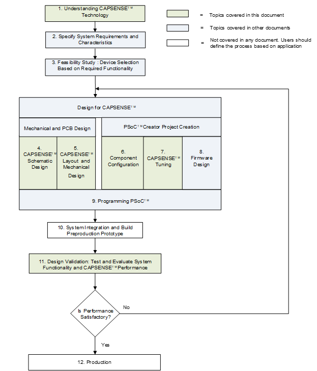
CAPSENSE™ design flow
illustrates the product design cycle with capacitive sensing; the information in this guide is highlighted in green. provides links to the supporting documents for each of the numbered tasks in
Figure 1
.
Figure 1. CAPSENSE™ product design flow
Steps in flowchart | Supporting documentation | |
|---|---|---|
Name | Chapter | |
| CAPSENSE™ design guide (This document) | – |
| Getting started with CAPSENSE™ | – |
| – | |
AN64846 – Getting started with CAPSENSE™ design guide AN79953 – Getting started with PSOC™ 4 | – | |
| CAPSENSE™ design guide (This document) | Design considerations |
| CAPSENSE™ design guide (This document) | Design considerations |
| PSOC™ CAPSENSE™ Component datasheet/middleware document | – |
CAPSENSE™ design guide (This document) | CAPSENSE™ performance tuning | |
| PSOC™ CAPSENSE™ design guide (This document) | CAPSENSE™ performance tuning |
| – | |
PSOC™ Creator Download ModusToolbox™ here . See the ModusToolbox™ related documents: ModusToolbox™ quick start guide ModusToolbox™ CAPSENSE™ configurator guide | – | |
| PSOC™ Creator user guide for in-IDE programming PSOC™ Programmer home page and MiniProg3 user guide for standalone programming | – |
| – | – |
| CAPSENSE™ design guide (This document) | CAPSENSE™ performance tuning |
| – | – |
CAPSENSE™ technology
Capacitive touch sensing technology measures changes in capacitance between a plate (the sensor) and its environment to detect the presence of a finger on or near a touch surface.
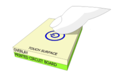
CAPSENSE™ fundamentals
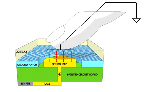
A typical CAPSENSE™ sensor consists of a copper pad of proper shape and size etched on the surface of a PCB. A non-conductive overlay serves as the touch surface for the button, as
Figure 2
shows.
Figure 2. Capacitive touch sensor
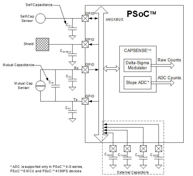
PCB traces and vias connect the sensor pads to PSOC™ GPIOs that are configured as CAPSENSE™ sensor pins. As Figure 3 shows, the self-capacitance of each electrode is modeled as CSX and the mutual capacitance between electrodes is modeled as C MX . CAPSENSE™ circuitry internal to the PSOC™ converts these capacitance values into equivalent digital counts (see PSOC™ 4 and PSOC™ 6 MCU CAPSENSE™ for details). These digital counts are then processed by the CPU to detect touches.
CAPSENSE™ also requires external capacitor
C
MOD
or
C
INT
for self-capacitance sensing and mutual-capacitance sensing. For third- and fourth-generation CAPSENSE™ architecture, a single
C
MOD
capacitor is required for self-capacitance sensing and
C
INTA
and
C
INTB
capacitors for mutual-capacitance sensing. If shield electrode is implemented for liquid tolerance, or for large proximity sensing distance, an additional
C
TANK
capacitor may be required. For Fifth-Generation CAPSENSE™ architecture, two
C
MOD
capacitors are required for both self-capacitance and mutual-capacitance sensing for each channel. These external capacitors are connected between a dedicated GPIO pin and ground.
Table 39
list the recommended values of the external capacitors.
Figure 3. PSOC™ device, sensors, and external capacitors
The capacitance of the sensor in the absence of a touch is called the parasitic capacitance,
C
P
.
C
P
results from the electric field between the sensor (including the sensor pad, traces, and vias) and other conductors in the system such as the ground planes, traces, and any metal in the product’s chassis or enclosure. The GPIO and internal capacitances of PSOC™ also contribute to the parasitic capacitance. However, these internal capacitances are typically very small compared to the sensor capacitance.
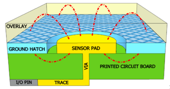
Self-capacitance sensing
shows how a GPIO pin is connected to a sensor pad by traces and vias for self-capacitance sensing. Typically, a ground (GND) hatch surrounds the sensor pad to isolate it from other sensors and traces. Although
Figure 4
shows some field lines around the sensor pad, the actual electric field distribution is very complex.
Figure 4. Parasitic capacitance
When a finger is present on the overlay, the conductive nature and large mass of the human body forms a grounded, conductive plane parallel to the sensor pad, as
Figure 5
shows.
Figure 5. Finger capacitance
This arrangement forms a parallel plate capacitor. The capacitance between the sensor pad and the finger is shown in
Equation 1
.
Figure 6. Finger capacitance
Where:
ε 0
= Free space permittivity
ε r
= Relative permittivity of overlay
A = Area of finger and sensor pad overlap
d = Thickness of the overlay
C F
= Finger capacitance.
C P
and
C
F
are parallel to each other because both represent the capacitance between the sensor pin and ground. Therefore, the total capacitance
C
S
of the sensor, when the finger is present on the sensor, is the sum of
C
P
and
C
F
.
Figure 7. Total sense capacitance when finger is present on sensor
In the absence of touch,
C
S
is equal to
C
P
.
PSOC™ converts the capacitance CS into equivalent digital counts called raw counts. Because a finger touch increases the total capacitance of the sensor pin, an increase in the raw counts indicates a finger touch. Refer to the CSD specification in
Device datasheet
/
Component datasheet/middleware document
document to learn about the supported CP range for a given device with which the recommended SNR can be achieved.
Mutual-capacitance sensing
shows the button sensor layout for mutual-capacitance sensing. Mutual-capacitance sensing measures the capacitance between two electrodes, transmit (Tx) electrode and receive (Rx) electrode.
In a mutual-capacitance sensing system, a digital voltage signal switching between VDDIO
2
or VDDD
3
(if VDDIO is not supported by the device) and GND is applied to the Tx pin and the amount of charge received on the Rx pin is measured. The amount of charge received on the Rx electrode is directly proportional to the mutual-capacitance (
C
M
) between the two electrodes.
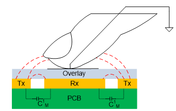
When a finger is placed between the Tx and Rx electrodes, the mutual-capacitance decreases to C
1
M
, as shown in
Figure 9
. Because of the reduction in the mutual-capacitance, the charge received on the Rx electrode also decreases. The CAPSENSE™ system measures the amount of charge received on the Rx electrode to detect a touch/no touch condition.
Figure 8. Mutual-capacitance sensing
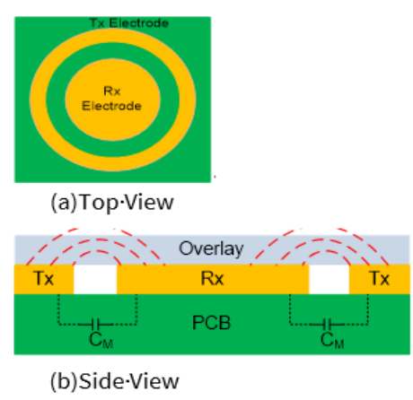
Figure 9. Mutual-capacitance with finger touch
Capacitive touch sensing method
PSOC™ uses patented capacitive touch-sensing method CAPSENSE™ sigma delta (CSD) for self-capacitance sensing and CAPSENSE™ crosspoint (CSX) for mutual-capacitance scanning. The CSD and CSX touch sensing methods provide the industry’s best-in-class
Signal-to-noise ratio (SNR)
. These sensing methods are a combination of hardware and firmware techniques.
CAPSENSE™ sigma delta (CSD)
shows a simplified block diagram of the CSD method.
In CSD, each GPIO has a switched-capacitance circuit that converts
C
s
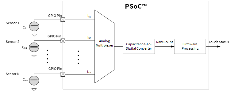
into an equivalent current. An analog MUX (AMUX) selects one of the sensor currents and feeds it into the current to digital converter. The current to digital converter is similar to a delta sigma ADC. The output count of the current to digital converter, known as raw count, is a digital value that is proportional to the self-capacitance between the electrodes.
Figure 10. Raw count and sensor capacitance relationship in CSD
Where,
G CSD
= Capacitance to digital conversion gain of CSD
C S
= Self-capacitance of the electrode
Figure 11. Simplified diagram of CSD method
illustrates a plot of raw count over time. When a finger touches the sensor, the
C
S
increases from
C
P
to
C
P
+
C
F
, and the raw count increases. By comparing the change in raw count to a predetermined threshold, logic in firmware decides whether the sensor is active (finger is present).
CAPSENSE™ crosspoint (CSX)
shows the simplified block diagram of the CSX method.
Figure 12. Simplified diagram of CAPSENSE™ crosspoint (CSX) method
With CSX, a voltage on the Tx electrode couples charge on to the RX electrode. This charge is proportional to the mutual capacitance between the Tx and Rx electrodes. An analog MUX then selects one of the Rx electrodes and feeds it into the current to digital converter.
The output count of the current to digital converter, , is a digital value that is proportional to the mutual-capacitance between the Rx and Tx electrodes as shown in Figure 13.
Figure 13. Raw count and sensor capacitance relationship in CSX
Where,
G C SX
= Capacitance to digital conversion gain of mutual capacitance method
C M
= Mutual-capacitance between two electrodes
illustrates a plot of raw count over time. When a finger touches the sensor,
C
M
decreases from
C
M
to
C
1
M
(see
Figure 9
) hence the counter output decreases. The firmware normalizes the raw count such that the raw counts go high when
C
M
decreases. This maintains the same visual representation of raw count between CSD and CSX methods. By comparing the change in raw count to a predetermined threshold, logic in firmware decides whether the sensor is active (finger is present). The normalized inverted raw count is computed using
Figure 58
.
Figure 14. Raw count versus time
For an in-depth discussion of the PSOC™ 4 and PSOC™ 6 CAPSENSE™ CSD and CSX blocks, see chapter PSOC™ 4 and PSOC™ 6 MCU CAPSENSE™.
Signal-to-noise ratio (SNR)
In practice, the raw counts vary due to inherent noise in the system.CAPSENSE™ noise is the peak-to-peak variation in raw counts in the absence of a touch, as
Figure 15
shows.
A well-tuned CAPSENSE™ system reliably discriminates between the ON and OFF states of the sensors. To achieve good performance, the CAPSENSE™ signal must be significantly larger than the CAPSENSE™ noise. SNR is defined as the ratio of CAPSENSE™ signal to CAPSENSE™ noise is the most important performance parameter of a CAPSENSE™ sensor.
Figure 15. SNR
In this example, the average level of raw count in the absence of a touch is 5925 counts. When a finger is placed on the sensor, the average raw count increases to 6060 counts, which means the signal is 6060– 5925 = 135 counts. The minimum value of the raw count in the OFF state is 5912 and the maximum value is 5938 counts. Therefore, the CAPSENSE™ noise is 5938 – 5912 = 26 counts. This results in an SNR of 135/26 = 5.2.
The minimum SNR recommended for a CAPSENSE™ sensor is 5. This 5:1 ratio comes from best practice threshold settings, which enable enough margin between signal and noise in order to provide reliable ON/OFF operation.
CAPSENSE™ widgets
CAPSENSE™ widgets consist of one or more CAPSENSE™ sensors, which as a unit represent a certain type of user interface. CAPSENSE™ widgets are broadly classified into four categories – buttons (zero-dimensional), sliders (one-dimensional), touchpads/trackpads (two-dimensional), and proximity sensors (three-dimensional).
Figure 16
shows button, slider, and proximity sensor widgets. This section explains the basic concepts of different CAPSENSE™ widgets. For a detailed explanation of sensor construction, see
Sensor construction
.
Figure 16. Several types of widgets
Buttons (zero-dimensional)
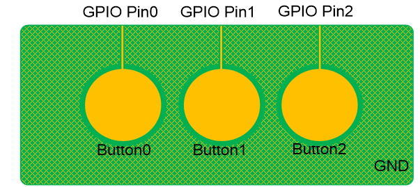
CAPSENSE™ buttons replace mechanical buttons in a wide variety of applications such as home appliances, medical devices, white goods, lighting controls, and many other products. It is the simplest type of CAPSENSE™ widget, consisting of a single sensor. A CAPSENSE™ button gives one of two possible output states: active (finger is present) or inactive (finger is not present). These two states are also called ON and OFF states, respectively.
For the self-capacitance (CSD) sensing method, a simple CAPSENSE™ button consists of a circular copper pad connected to a PSOC™ GPIO with a PCB trace. The CAPSENSE™ button is surrounded by grounded copper hatch that isolates it from other buttons and traces. A circular gap separates the button pad and the ground hatch. Each button requires one PSOC™ GPIO. These buttons can be constructed using any conductive material on a non-conductive substrate; for example, indium tin oxide on a glass substrate, or silver ink on a non-conductive film. Even metallic springs can be used as button sensors; see
Sensor construction
for more details.
Figure 17. Simple CAPSENSE™ buttons
For the mutual-capacitance (CSX) sensing method, each button requires one GPIO pin configured as Tx electrode and one GPIO pin configured as Rx electrode.The Tx pin and Rx pins can be shared across multiple buttons, with each button being a unique intersection of Rx and Tx like in
Figure 18
.However, it is recommended to minimize the Rx trace length and shield the Rx trace with ground on both sides, to minimize noise coupling into the Rx.
Figure 18. Simple CAPSENSE™ buttons for mutual-capacitance sensing method

If the application requires many buttons (for example in a calculator keypad or a QWERTY keyboard), you can arrange the CAPSENSE™ buttons in a matrix, as
Figure 19
shows. This allows a design to have multiple buttons per GPIO. For example, the 16-button design in
Figure 19
requires only eight GPIOs.
Figure 19. Matrix buttons based on CSD
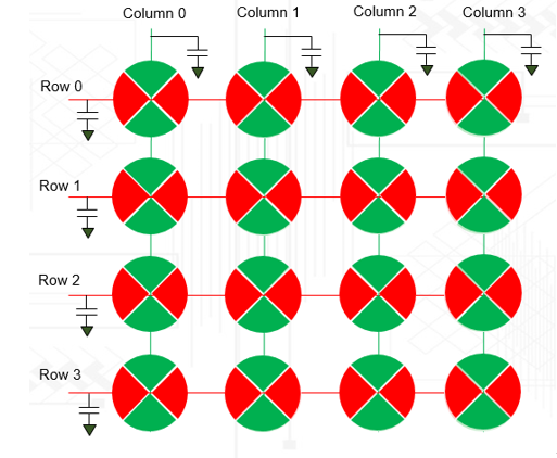
A matrix button design has two groups of capacitive sensors: row sensors and column sensors. The matrix button architecture can be used for both self-capacitance (CSD) and mutual-capacitance (CSX) methods.
In CSD mode, each button consists of a row sensor and a column sensor, as
Figure 19
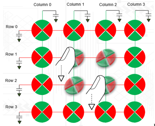
shows. When a button is touched, both row and column sensors of that button become active. The CSD-based matrix button should be used only if the user is expected to touch one button at a time. If the user touches more than one diagonally opposite buttons, the finger location cannot be resolved as
Figure 20
shows. This effect is called as ghost effect, which is considered an invalid condition.
Figure 20. Ghost effect in matrix button based on CSD
Mutual-capacitance is the recommended sensing method for matrix buttons because this method is not affected from the ghost touch phenomena and provides better SNR for high
C
p
sensors. This is because it senses mutual-capacitance formed at each intersection rather than sensing rows and columns as shown in
Figure 21
. Applications that require simultaneous sensing of multiple buttons, such as a keyboard with
Shift
,
Ctrl
, and
Alt
keys can use CSX sensing method or you should design the
Shift
,
Ctrl
, and
Alt
keys as individual CSD buttons.
Figure 21. Matrix button based on CSX
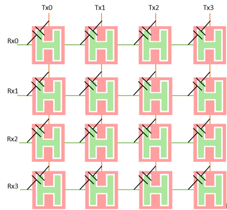
Note: Scanning a matrix keypad using CSX sensing method may require a longer overall scan time than the CSD sensing method. This is because the CSD sensing method scans rows and columns as sensors, while the CSX sensing method scans each intersection as a sensor.
Sliders (one-dimensional)
Sliders are used when the required input is in the form of a gradual increment or decrement. Examples include lighting control (dimmer), volume control, graphic equalizer, and speed control. Currently, the CAPSENSE™ Component in PSOC™ Creator and ModusToolbox™ supports only self-capacitance-based sliders. Mutual capacitance-based sliders will be supported in future version of component.
A slider consists of a one-dimensional array of capacitive sensors called segments, which are placed adjacent to one another. Touching one segment also results in partial activation of adjacent segments. The firmware processes the raw counts from the touched segment and the nearby segments to calculate the position of the geometric center of the finger touch, which is known as the
centroid position
.
The actual resolution of the calculated centroid position is much higher than the number of segments in a slider. For example, a slider with five segments can resolve at least 100 physical finger positions. This high resolution gives smooth transitions of the centroid position as the finger glides across a slider.
In a linear slider, the segments are arranged inline, as
Figure 22
shows. Each slider segment connects to a PSOC™ GPIO. A zigzag pattern (double chevron) is recommended for slider segments. This layout ensures that when a segment is touched, the adjacent segments are also partially touched, which aids estimation of the centroid position.
Figure 22. Linear slider
Radial sliders are similar to linear sliders except that radial sliders are continuous.
Figure 23
shows a typical radial slider.
Figure 23. Radial slider
Touchpads/Trackpads (two-dimensional)
A touchpad (also known as trackpad) has two linear sliders arranged in an X and Y pattern, enabling it to locate a finger’s position in both X and Y dimensions.
Figure 24
shows a typical arrangement of a touchpad sensor. Similar to the matrix buttons, touchpads can also be sensed using either CSD or CSX sensing method.
CSD-based touchpads suffer from ghost touches, so it supports only single-point touch applications.
CSX touchpads can support multi-point touch applications, but these may need more scanning time compared to CSD touchpad because this method scans each intersection rather than rows and columns.
Figure 24. Touchpad sensor arrangement
See
AN234185 PSOC™ 4 CAPSENSE™ Touchpad design guide
to learn more.
Proximity (three-dimensional)
Proximity sensors detect the presence of a hand in the three-dimensional space around the sensor. However, the actual output of the proximity sensor is an ON/OFF state similar to a CAPSENSE™ button. Proximity sensing can detect a hand at a distance of several centimeters to tens of centimeters depending on the sensor construction. Self capacitance is the recommended method of sensing for a proximity application.
Proximity sensing requires electric fields that are projected to much larger distances than buttons and sliders. This demands a large sensor area. However, a large sensor area also results in a large parasitic capacitance
C
P
, and detection becomes more difficult. This requires a sensor with high electric field strength at large distances while also having a small area.
Figure 25
shows a proximity sensor using a trace with a thickness of 2-3 mm surrounding the other sensors.
Figure 25. Proximity sensor
You can also implement a proximity sensor by ganging other sensors together. This is accomplished by combining multiple sensor pads into one large sensor using firmware. The disadvantage of this method is high parasitic capacitance. See the
Component datasheet/middleware document
for details on maximum parasitic capacitance supported by a given device.
See
AN92239 proximity sensing with CAPSENSE™
and the proximity sensing section in
Getting started with CAPSENSE™ design guide
to learn more about proximity sensors.
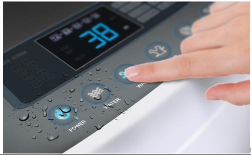
Liquid tolerance
Capacitive sensing is used in a variety of applications such as home appliances, automotive, and industrial applications. These applications require robust capacitive-sensing operation even in the presence of mist, moisture, water, ice, humidity, or other liquids. In a capacitive-sensing application design, false sensing of touch or proximity detection may happen due to the presence of a film of liquid or liquid droplets on the sensor surface, due to the conductive nature of some liquids. CSD sensing method can compensate for variation in raw count due to these causes and provide a robust, reliable, capacitive sensing application operation.
Figure 26. Liquid-tolerant CAPSENSE™-based touch user interface in washing machine
To compensate for changes in raw count due to mist, moisture, and humidity changes, the CAPSENSE™ sensing method continuously adjusts the baseline of the sensor to prevent false triggers
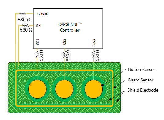
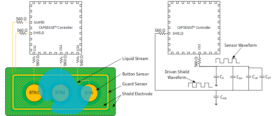
To prevent sensor false triggers due to a liquid flow, you should implement a Guard sensor as Figure 27 shows. The Driven shield signal and shield electrode can be used to detect the presence of a streaming liquid and ignore the status or stop the sensing from rest of the sensors as long as the liquid flow is present
Note: the guard sensor itself is just another self-capacitance sensor; even though you could implement it around mutual-capacitance sensors also for liquid flow tolerance. PSOC™ devices allow implementation of such self-capacitance sensors and mutual-capacitance sensors together in the same design
To compensate for changes in raw count due to liquid droplets for self-capacitance sensing, you can implement a Driven shield signal and shield electrode as Figure 27 shows. When a shield electrode is implemented, CAPSENSE™ reliably works and reports the sensor ON/OFF status correctly, even when liquid droplets are present on the sensor surface. To prevent sensor false triggers due to liquid droplets for mutual-capacitance sensing, you can use both the sensing methods that is, mutual capacitance and self-capacitance with Driven shield signal and shield electrode on the same set of sensors as Using self-capacitance sensing for liquid tolerance of mutual-capacitance sensors explains
In summary, if your application requires tolerance to liquid droplets, implement a
Driven shield signal and shield electrode
. If your application requires tolerance to streaming liquids along with liquid droplets, implement a
Driven shield signal and shield electrode
and a
Guard sensor
as shown in
Figure 27
. Follow the schematic and layout guidelines explained in the
Layout guidelines for liquid tolerance
section to construct the shield electrode and guard sensor respectively.
Figure 27. Shield electrode (SH) and guard sensor (GUARD) connected to CAPSENSE™ controller
Liquid tolerance for self capacitance sensing
Effect of liquid droplets and liquid stream on a self-capacitance sensor
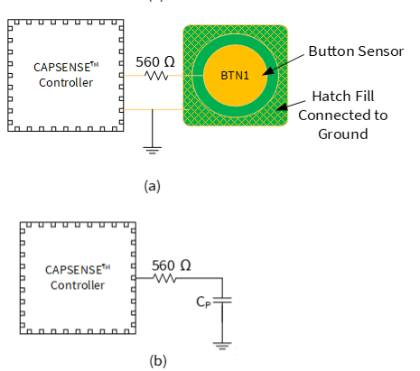
To understand the effect of liquids on a CAPSENSE™ sensor, consider a CAPSENSE™ system in which the hatch fill around the sensor is connected to ground, as
Figure 28
(a) shows. The hatch fill when connected to a GND improves the noise immunity of the sensor. Parasitic capacitance of the sensor is denoted as
C
P
in
Figure 28
(b).
Figure 28. Typical CAPSENSE™ system layout
As shown in
Figure 29
, when a liquid droplet falls on the sensor surface, due to its conductive nature it provides a strong coupling path for the electric field lines to return to ground; this adds a capacitance
C
LD
in parallel to
C
P
. This added capacitance draws an additional charge from the AMUX bus as explained in
GPIO cell capacitance to current converter
resulting in an increase in the sensor raw count. In some cases (such as salty water or water containing minerals), the increase in raw count when a liquid droplet falls on the sensor surface may be equal to the increase in raw count due to a finger touch, as
Figure 29
shows. In such a situation, sensor false triggers might occur.
Figure 29. Capacitance added by liquid droplet when the Hatch Fill is connected to GND
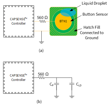
C P
= Sensor parasitic capacitance
C LD
= Capacitance added by the liquid droplet
Figure 30. Effect of liquid droplet when the Hatch Fill around the sensor is connected to GND
To nullify the effect of capacitance added by the liquid droplet to the CAPSENSE™ circuitry, you should drive the hatch fill around the sensor with the
driven-shield signal
.
As
Figure 31
shows, when the hatch fill around the sensor is connected to the driven-shield signal and when a liquid droplet falls on the touch interface, the voltage on both sides of the liquid droplet remains at the same potential. Because of this, the capacitance,
C
LD
, added by the liquid droplet does not draw any additional charge from the AMUX bus and hence the effect of capacitance
C
LD
is nullified. Therefore, the increase in raw count when a water droplet falls on the sensor will be very small, as
Figure 32
shows.
Figure 31. Capacitance added by liquid droplet droplet when the hatch fill around the sensor is connected to shield
C S
= Sensor parasitic capacitance
C SH
= Capacitance between the sensor and the hatch fill
C HG
= Capacitance between the hatch fill and ground
C LD
= Capacitance added by the liquid droplet
Figure 32. Effect of liquid droplet when the hatch fill around the sensor is connected to the driven-shield
shows how a sensor may false trigger in presence of a liquid, if hatch fill is connected to ground. Note however, that the same is not true for all cases. For example,
spring sensors
, which are inherently more liquid tolerant than sensors etched on PCB surface. As
Figure 33
shows, due to the large airgap between the liquid drop and the hatch fill, the capacitance
C
LD
between the liquid drop and grounded hatch pattern on the PCB would be very low so as not to cause any false triggers. If required, the hatched pattern on the PCB can still be connected to a driven shield electrode to further nullify the effect of
C
LD
and have an improved liquid tolerance.
Figure 33. Capacitance added by liquid droplet in spring sensor
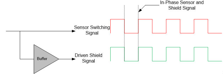
Driven shield signal and shield electrode
The driven-shield signal is a buffered version of the sensor-switching signal, as
Figure 34
shows. The driven-shield signal has the same amplitude, frequency, and phase as that of sensor switching signal. When the hatch fill around the sensor is connected to the driven shield signal, it is referred as shield electrode.
Figure 34. Driven shield signal
To implement liquid-tolerant CAPSENSE™ designs: Shield electrode helps in making CAPSENSE™ designs liquid-tolerant as explained above
To improve proximity sensing distance in presence of floating or grounded conductive objects: A shield electrode, when placed between the proximity sensor and a floating or a grounded conductive object, reduces the effect of these objects on the proximity-sensing distance and helps in achieving large proximity-sensing distance. See the “Proximity Sensing” section in the Getting started with CAPSENSE™ design guide for more details
To reduce the parasitic capacitance of the sensor: When a CAPSENSE™ sensor has a long trace, the CP of the sensor will be very high because of the increased coupling of sensor electric field lines from the sensor trace to the surrounding ground. By implementing a shield electrode, the coupling of electric field lines to ground is reduced, which results in reducing the CP of the sensor
See
Layout guidelines for shield electrode
for layout guidelines of shield electrode.
Guard sensor
When a continuous liquid stream is present on the sensor surface, the liquid stream adds a large capacitance (
C
ST
) to the CAPSENSE™ sensor. This capacitance may be several times larger than
C
LD
. Because of this, the effect of the shield electrode is completely masked, and the sensor raw counts will be same as or even higher than a finger touch. In such situations, a guard sensor is useful to prevent sensor false triggers.
A guard sensor is a copper trace that surrounds all the sensors on the PCB, as
Figure 35
shows. A guard sensor is similar to a button sensor and is used to detect the presence of streaming liquids. When a guard sensor is triggered, the firmware should disable the scanning of all other sensors except the guard sensor to prevent sensor false triggers.
Note: The sensors are not scanned, or the sensor status is ignored when the guard sensor is triggered; therefore, touch cannot be detected when there is a liquid stream on the touch surface.
Figure 35. Measurement with a liquid stream
See
Layout guidelines for guard sensor
for PCB layout guidelines for implementing a guard sensor.
If there is no space on the PCB for implementing a guard sensor, the guard sensor functionality can be implemented in the firmware. For example, you can use the ON/OFF status of different sensors to detect a liquid stream depending on the use case, such as follows:
When there is a liquid stream, more than one button sensor will be active at a time. If your design does not require multi-touch sensing, you can detect this and ignore the sensor status of all the button sensors to prevent false triggering
In a slider, if the slider segments which are turned ON are not adjacent segments, you can reset the slider segments status or ignore the slider centroid value that is calculated
Likewise, you could create your own custom algorithm to detect the presence of streaming liquids and ignore the sensor status during the time a liquid is present on the touch surface
Note: The sensors are not scanned, or the sensor status is ignored when the guard sensor is triggered; therefore, touch cannot be detected when there is a liquid stream on the touch surface
Liquid tolerance for mutual-capacitance sensing
Effect of liquid droplets and liquid stream on a mutual-capacitance sensor
Mutual-capacitance buttons often have a grounded hatch fill around the sensors for improved noise immunity. If a liquid droplet falls over the sensor while covering some part of the grounded hatch, the mutual-capacitance decreases similar to the effect of placing a finger on the sensor. This decrease in mutual-capacitance causes an increase in raw count as explained in CAPSENSE™ CSX sensing method (third- and fourth- generation) in and as shown in the Figure 36 . The amount of increase in the raw count depends on the size and characteristics of the liquid drop.
However, mutual-capacitance increases if the liquid droplet covers just the Tx and Rx electrode and does not spread over the grounded hatch. This causes a decrease in raw count as shown in
Figure 36
. This decrease in raw count may cause the baseline reset due to
Low baseline reset
. Once the liquid drop is removed, the raw count would rise while the baseline may remain at the lower value, resulting in a difference signal which may cause the sensor to false trigger.
Figure 36. Effect of liquid droplet on CSX sensor when the Hatch Fill around the sensor is connected to ground
Using self-capacitance sensing for liquid tolerance of mutual-capacitance sensors
CAPSENSE™ senses the self-capacitance of Tx and Rx nodes of a mutual-capacitance sensor. This ability of scanning the sensor using both CSD and CSX modes could be used to avoid false triggers due to the presence of liquid drops on a mutual capacitance sensor. See the code example
PSOC™ 4 hybrid sensing using CAPSENSE™
to understand how to sense a mutual-capacitance button with both CSD as well as CSX sensing method.
To achieve liquid tolerance, you need to scan the Rx electrode of the sensor
with the CSD sense method. While scanning the Rx electrode as a CSD sensor, ensure that
you enable the shield electrode, and connect the Tx pin of the mutual-capacitance sensor
to the driven shield signal. You can use the low-level API function
CapSense_SetPinState()
to connect the Tx pin of the
mutual-capacitance sensor to the shield electrode before calling the
CapSense_ScanAllWidgets()
API function that scans the
Rx electrode as a CSD sensor as shown
below:
CapSense_SetPinState(CapSense_BUTTON1_WDGT_ID,CapSense_BUTTON1_TX0_ID,CapSense_SHIELD);
CapSense_ScanAllWidgets();
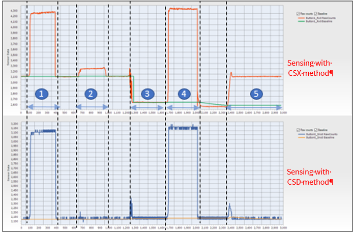
From sections
2.5.1
and
2.5.2
you understood the effect of liquid drop on the CSD and CSX button respectively. By utilizing the difference in their response to the liquid drop, you can create a firmware logic to achieve a liquid-tolerant mutual-capacitance sensor. The effect of presence of the liquid drop on the CSD and CSX scan results is summarized in
Figure 37
.
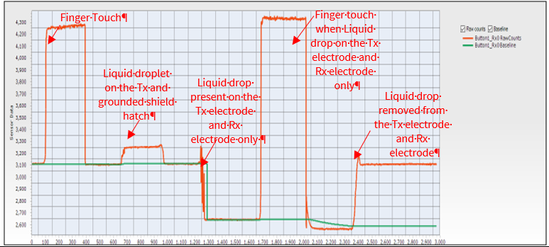
Figure 37. Effect of water drop on the CSX sensor pattern scanned with CSD and CSX methods
Where
Figure 37
shows the effect of the water drop on the CSX sensor pattern surrounded by hatch fill when scanned using this method. The regions in
Figure 37
represent the following:
Finger touch
Liquid droplet on the Tx line and grounded shield hatch
Liquid drop present on the Tx and Rx electrodes only
Finger touch when a liquid drop is on the Tx and Rx electrodes only
Liquid drop removed from the Tx and Rx electrodes
The changes in raw count as shown in
Figure 37
can be used in the firmware to reset the baseline of the CSX sensor to nullify the effect of liquid drops. The button status should be ON state for Region 1, 4, and OFF state in other regions; additionally, the baseline of the CSX button must be re-initialized in Region 3 and Region 5. The baseline of the sensor could be reset by using the
CapSense_InitializeWidgetBaseline()
API function as shown below:
CapSense_InitializeWidgetBaseline(CapSense_CSX_BUTTON_WDGT_ID);
See the Component datasheet/middleware document or more details on using this API; see Selecting CAPSENSE™ software parameters to learn about the baseline of the sensor.
Effect of liquid properties on liquid-tolerance performance
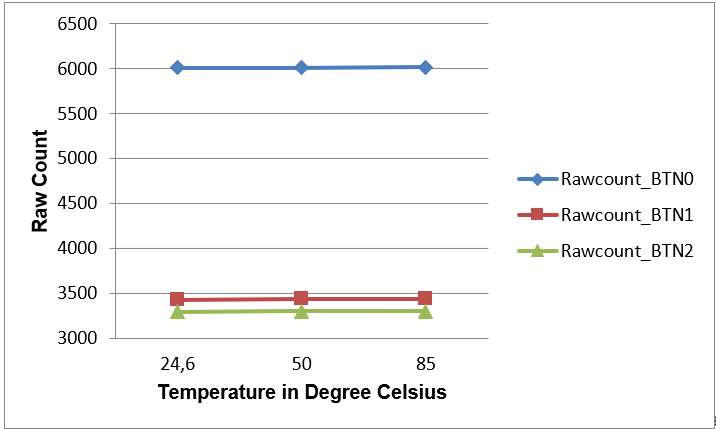
In certain applications, the CAPSENSE™ system has to work in the presence of a variety of liquids such as soap water, sea water, and mineral water. In such applications, it is always recommended to tune the CAPSENSE™ parameters for sensors by considering the worst-case signal due to liquid droplets. To simulate the worst-case conditions, it is recommended that you test the liquid-tolerance performance of the sensors with salty water by dissolving 40 grams of cooking salt (NaCl) in one liter of water. Tests were done using soapy water; the results show that the effect of soapy water is similar to the effect of salty water. Therefore, if the tuning is done to reject salty water, the CAPSENSE™ system will work even in the presence of soapy water.
In applications such as induction cooktops, there are chances of hot water spilling on to the CAPSENSE™ touch surface. To determine the impact of the temperature of a liquid droplet on CAPSENSE™ performance, droplets of water at different temperatures were poured on a sensor and the corresponding change in raw counts was monitored. Experiment shows that the effect of hot liquid droplets is same as that of the liquid at room temperature as
Figure 38
shows. This is because the hot liquid droplet cools down immediately to room temperature when it falls on the touch surface. If hot water continuously falls on the sensor and the temperature of the overlay rises because of the hot water, the increase in raw count due to the increase in temperature is compensated by the
Baseline update algorithm
, thereby preventing any false triggering of the sensors.
Figure 38. Raw count variation versus water temperature
PSOC™ 4 and PSOC™ 6 MCU CAPSENSE™
This chapter explains how CAPSENSE™ CSD and CSX (third, fourth, and fifth generations) are implemented in the PSOC™ 4 and PSOC™ 6 MCUs. See
Capacitive touch sensing method
to understand the basic principles of CAPSENSE™. A basic knowledge of the PSOC™ device architecture is a prerequisite for this chapter. If you are new to PSOC™ 4, see
AN79953 - Getting started with PSOC™ 4
or
AN91267 - Getting started with PSOC™ 4 Bluetooth® LE
; for PSOC™ 6 MCU, see
AN221774 - Getting started with PSOC™ 6 MCU
.
You can skip this chapter if you are using the automatic tuning feature (SmartSense) of the Component. See the CAPSENSE™ performance tuning chapter for details.
The PSOC™ 4 family of devices has three different CAPSENSE™ architectures.
Table 2
explains the differences between the third and fifth-generation CAPSENSE™ architecture.
CAPSENSE™ generations in PSOC™ 4 and PSOC™ 6
lists the main differences in the CAPSENSE™ architecture for CSD and CSX.
Feature | Third-generation CAPSENSE™ | Fourth-generation CAPSENSE™ | Fifth-generation CAPSENSE™ | Improvement impact | Conditions | |
|---|---|---|---|---|---|---|
SNR | 5:1 | 6.5:1 | 48:1 | Higher SNR implies better sensitivity, that is, ability to sense smaller signals. | VDD = 5 V No firmware filter; C p ~= 33 pF; Cf = 0.1 pF | |
Sensing mode | Self-cap and mutual-cap modes | Self-cap, mutual-cap, and ADC modes | Self-cap and mutual-cap modes | – | – | |
Sensor capacitance parasitic range | 5 pF – 45 pF | 5 pF – 200 pF | 2 pF – 200 pF | Greater C p range implies higher flexibility in PCB layout routing and ability to sense with very short/long sensor traces, and for different PCB materials (for example, FFC and so on). | – | |
Typical sense signal needed | 100 fF | 100 fF | 15 fF for CSD-RM 10 fF for CSX-RM | Smaller sense signal required, implying support for thicker overlays, higher proximity range, smaller sensor size, and so on. | V DD = 5 V; No firmware filter; C p ~= 33 pF; SNR = 5:1; | |
Noise floor (rms) | – | – | 500 aF for CSD-RM 100 aF for CSX-RM | Higher SNR or lower noise floor implies ability to sense smaller signals. | V DD - 5 V; C p ~= 33 pF; C M = 5 pF | |
Overlay thickness supported | Up to 5 mm | Up to 5 mm | Up to 18 mm | Supports designs with thicker overlay. | 10 mm CSD button; Acrylic overlay; SNR = 5:1; C p ~= 22 pF; | |
Refresh rate | – | 22 Hz | 242 Hz | Faster refresh rate enables fast gestures and taps detections on applications such as large trackpad and long sliders or large number of button sensors with single device, and so on. | 7x5 CSX touchpad; Acrylic overlay 3 mm thickness; SNR = 10:1; Finger Size = 8 mm; | |
CPU bandwidth requirement | Completely CPU driven. CPU is required for initialization and sequencing the sensors. | 40% sequencer 4 It takes care of initialization, configuration, and scanning of sensors. CPU is needed for sequencing through each sensor. | 7% Completely autonomous. | Reduced CPU usage for sensing frees the CPU to perform other peripheral operations, and act as a central controller in an application. | 10x8 CSX touchpad; Scan clock = 1 MHz; No of sub-conversions = 70; Refresh rate = 100 Hz; | |
Emission control options. | PRS | PRS, SSC | PRS, SSC | – | – | |
Noise immunity | Sense Voltage ( Vref ) | 1.2 V | 1.2 V-2.8 V. | Rail to Rail | Higher the sense voltage, higher the noise immunity. | – |
Differential Sensing | Mutual-cap sensing | Mutual-cap sensing | Mutual-cap and self-cap sensing | Differential sensing cancels out noise induced from external environment through CMOD. | ||
VDD noise impact | Yes | Yes | No | VDD noise has minimal affect on fifth generation CAPSENSE™ operation. | ||
Sense clock frequency | Self-Cap | 45 kHz – 6 MHz | 45 kHz – 6 MHz | 45 kHz – 6 MHz | Higher sense clock frequency means faster scan for low C p sensors. This provides ability to support faster taps or gestures, or for a given refresh rate, ability to implement multiple firmware filters for better immunity. | – |
Mutual-Cap | 45 kHz - 300 kHz | 45 kHz - 3 MHz | 45 kHz – 6 MHz | |||
Multi-channel support | No | No | Yes | Provides ‘n’ times increased speed of scanning for the same number of sensors, if ‘n’channels are used. | – | |
Shield Cp | -- | -- | 1.2 nF | – | – | |
Device family | PSOC™ 4100/4200 PSOC™ 4100 M/4200 M PSOC™ 4100 L/4200 L PSOC™ 4100 BL/4200 BL | PSOC™ 4000 PSOC™ 4000S PSOC™ 4100S PSOC™ 4100S Plus PSOC™ 6 | PSOC™ 4100S Max PSOC™ 4000T(fifth-generation low-power) PSOC™ 4100T Plus (fifth-generation low-power) | – | – | |
Capacitive Sigma-Delta (CSD) sensing method (third and fourth generation)
illustrates the CAPSENSE™ block that scans CAPSENSE™ sensors in the CSD sensing mode.
Figure 39. CAPSENSE™ CSD sensing
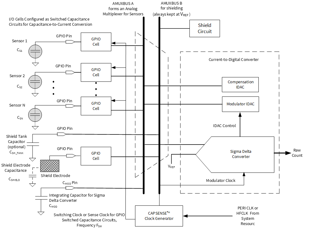
As explained in
Capacitive touch sensing method
, this block works by first converting the sensor capacitance into an equivalent current. An analog multiplexer then selects one of the currents and feeds it into the current-to-digital converter. This current-to-digital converter consists of a sigma-delta converter, which controls the modulation IDAC for a specific period, the total current sourced or sinked by the IDACs is the same as the total current sinked or sourced by the sensor capacitance. The digital count output of the sigma-delta converter is an indicator of the sensor capacitance and is called a raw count. This block can be configured in either IDAC Sourcing mode or IDAC Sinking mode. In the IDAC Sourcing mode, the IDACs source current to AMUXBUS while the GPIO cells sink current from AMUXBUS. In the IDAC Sinking mode, the IDACs sink current from AMUXBUS while the GPIO cells source current to AMUXBUS.
GPIO cell capacitance to current converter
In the CAPSENSE™ CSD system, the GPIO cells are configured as switched-capacitance circuits that convert sensor capacitances into equivalent currents.
Figure 40
shows a simplified diagram of the GPIO cell structure.
Figure 40. GPIO cell structure
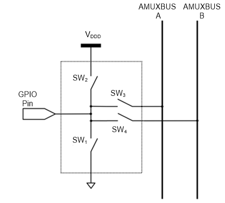
PSOC™ 4 and PSOC™ 6 devices consist of two AMUX buses: AMUXBUS A is used for CSD sensing and AMUXBUS B is used for CAPSENSE™ CSD shielding . The GPIO switched-capacitance circuit has two possible configurations: source current to AMUXBUS A or sink current from AMUXBUS A
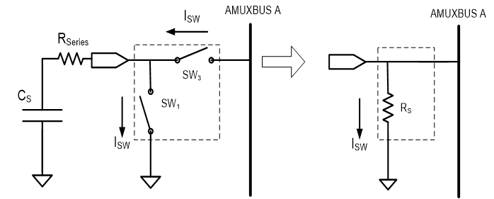
IDAC sourcing mode
In the IDAC Sourcing mode, the GPIO cell sinks current from the AMUXBUS A through a switched capacitor circuit as
Figure 41
shows.
Figure 41. GPIO cell sinking current from AMUXBUS A
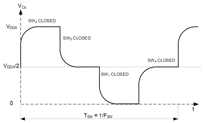
Two non-overlapping, out-of-phase clocks of frequency
F
SW
control the switches
SW
1
and
SW
3
as Figure 42 shows. The continuous switching of SW1 and SW3 forms an equivalent resistance
R
S
, as
Figure 41
shows.
Figure 42. SW 1 and SW3 switch in non-overlapping manner
If the switches operate at a sufficiently low frequency
F
SW
, such that time
T
SW
/2 is sufficient to fully charge the sensor to V
REF
and fully discharge it to ground, as
Figure 42
shows, the value of the equivalent resistance
R
S
is given by
Figure 43
.
Figure 43. Sensor equivalent resistance
Where,
C S
= Sensor capacitance
F SW
= Frequency of the sense clock
The sigma-delta converter maintains the voltage of AMUXBUS A at a constant
V
REF
(this process is explained in
Sigma-delta converter
.
Figure 44
shows the resulting voltage waveform across
C
S
.
Figure 44. Voltage across sensor capacitance
gives the value of average current taken from AMUXBUS A.
Figure 45. Average current sinked from AMUXBUS A to GPIO through CAPSENSE™ sensor (ICS)
IDAC sinking mode
In the IDAC sinking mode, the GPIO cell sources current to the AMUXBUS A through a switched capacitor circuit as
Figure 46
shows.
Figure 47
shows the voltage waveform across the sensor capacitance.
Because this mode charges the AMUXBUS A directly through
V
DDD
, it is more susceptible to power supply noise compared to the IDAC sourcing mode. Hence, it is recommended to use this mode with an LDO or a very stable and quiet V
DDD
.
Figure 46. GPIO cell sourcing current to AMUXBUS A
Figure 47. Voltage across sensor capacitance
provides the value of average current supplied to AMUXBUS A.
Figure 48. Average current sourced to AMUXBUS A from GPIO through CAPSENSE™ sensor (ICS)
CAPSENSE™ clock generator
The CAPSENSE™ clock generator block generates the sense clock
F
SW
, and the modulation clock
F
MOD
, from the high-frequency system resource clock (HFCLK) or peripheral clock (PERI) depending on the PSOC™ device family as shown in
Figure 39
.
Sense clock
The sense clock, also referred to as the switching clock, drives the non-overlapping clocks to the GPIO cell switched capacitor circuits for the
GPIO cell capacitance to charge converter
.
Sense clock can be sourced from three options: direct, 8-bit PRS, and 12-bit PRS. Some PSOC™ 4 and PSOC™ 6 MCU parts also support additional spread spectrum clock (SSCx) modes. For more details on the supported modes for PSOC™ device, see the
Component datasheet/middleware document
.
Direct clock is a constant frequency sense clock source. When you chose this option, the sensor pin switches with a constant frequency clock with frequency as specified in the CAPSENSE™ component configuration window.
PRS clock implies that the sense clock is driven from a PRS block, which can generate either 8-bit or 12-bit PRS. Use of the PRS clock spreads the sense clock frequency over a wide frequency range by dividing the input clock using a PRS.
SSCx also spreads the sense clock frequency. It provides better noise immunity and reduces radiated electromagnetic emissions.
See
Manually tuning hardware parameters
for details on the clock source and frequency selection guidelines.
Modulator clock
The modulation clock is used by the
Sigma-delta converter
. This clock determines the sensor scan time based on
Equation 8
and
Equation 9
.
Figure 49. Sensor scan time
Figure 50. Hardware scan time
Where,
Resolution =
Scan resolution
Sensor Initialization time = Time taken by the sensor to write to the internal registers and initiate a scan.
Sigma-delta converter
The sigma-delta converter converts the input current to a corresponding digital count. It consists of a sigma-delta converter and two current sourcing/sinking digital-to-analog converters (IDACs) called modulation IDAC and compensation IDAC as
Figure 39
shows.
The sigma-delta converter uses an external integrating capacitor, called modulator capacitor C MOD , as
Figure 39
shows. Sigma-delta converter controls the modulation IDAC current by switching it ON or OFF corresponding to the small voltage variations across
C
MOD
to maintain the
C
MOD
voltage at
V
REF
. The recommended value of
C
MOD
is listed in
Table 39
.
The sigma-delta converter can operate in either IDAC sourcing mode or IDAC sinking mode.
IDAC sourcing mode : In this mode, the GPIO cell capacitance to charge converter sinks current from C MOD through AMUXBUS A, and the IDACs then source current to AMUXBUS A to balance its voltage
IDAC sinking mode : In this mode,the GPIO cell capacitance to charge converter sources current from C MOD to AMUXBUS A and the IDACs sink current through AMUXBUS A to balance its voltage
In both the above-mentioned modes, the sigma delta converter can operate in either single IDAC mode or dual IDAC mode:
In the single IDAC mode, the modulation IDAC is controlled by the sigma-delta converter; the compensation IDAC is always OFF
In the dual IDAC mode, the modulation IDAC is controlled by the sigma-delta converter; the compensation IDAC is always ON
In the single IDAC mode, if ‘N’ is the resolution of the sigma-delta converter and
I
MOD
is the value of the modulation IDAC current, the approximate value of raw count in the IDAC Sourcing mode is given by
Equation 10
.
Figure 51. Single IDAC sourcing raw count
Similarly, the approximate value of raw count in the IDAC sinking mode is given by
Equation 11
.
Figure 52. Single IDAC sinking raw count
In both cases, the raw count is proportional to sensor capacitance C S . The raw count is then processed by the CAPSENSE™ CSD Component firmware to detect touches. The hardware parameters such as I MOD , ICOMP , and F SW , and the software parameters, should be tuned to optimum values for reliable touch detection. For an in-depth discussion of the tuning, see CAPSENSE™ performance tuning .
In the dual IDAC mode, the compensation IDAC is always ON. If
I
COMP
is the compensation IDAC current, the equation for the raw count in the IDAC sourcing mode is given by
Equation 12
.
Figure 53. Dual IDAC sourcing raw count
Raw count in the IDAC sinking mode is given by
Equation 13
.
Figure 54. Dual IDAC sinking raw count
Note: Raw count values are always positive. It is thus imperative to ensure thatICOMPis less than (VDD-VREF)CSFSWfor the IDAC sinking mode andICOMPis less thanCSFSWVREFfor the IDAC Sourcing mode.Equation 13does not hold true ifICOMP>VREFCSFSWandEquation 12does not hold true ifICOMP>(VDD-VREF)CSFSW; in these cases, raw counts will be zero.
The relation between the parameters shown in the above equation to the CAPSENSE™ Component parameters is listed in
Table 3
.
Sl. No. | Parameter | Description | Comments |
|---|---|---|---|
1 | N | Scan resolution | Scan resolution is configurable from 6-bit to 16-bit. See Component datasheet/middleware document for details. |
2 | VREF | N/A | The V REF value is 1.2 V or configurable between 0.6 V to V DDA - 0.6 V depending on the PSOC™ device family. See Component datasheet/middleware document for details. |
3 | FSW | Sense clock frequency | Sense clock frequency and sense clock source decide the frequency at which the sensor is switching. See Sense clock for details. |
Sense clock source | |||
4 | IMOD | Modulator IDAC | IMOD = Modulation IDAC current |
5 | I COMP | Compensation IDAC | I COMP = Compensation IDAC current |
6 | V DD | N/A | This parameter is the device supply voltage. |
7 | CS | N/A | This parameter is the sensor parasitic capacitance. |
8 | N/A | Modulator clock frequency | Modulator clock divider does not impact raw count. See the Modulator clock section for more details. |
Analog multiplexer (AMUX)
The sigma delta converter scans one sensor at a time. An analog multiplexer selects one of the GPIO cells and connects it to the input of the sigma delta converter, as
Figure 39
shows. The AMUXBUS A and the GPIO cell switches (see SW3 in
Figure 46
) forms this analog multiplexer. AMUXBUS A connects to all GPIOs that support CAPSENSE™. See the corresponding
Device datasheet
for a list of port pins that support CAPSENSE™. AMUXBUS A also connects the integrating capacitor
C
MOD
to the sigma-delta converter circuit. AMUXBUS B is used for shielding and is kept at V REF when shield is enabled.
CAPSENSE™ CSD shielding
PSOC™ 4 and PSOC™ 6 MCU CAPSENSE™ supports shield electrodes for liquid tolerance and proximity sensing. CAPSENSE™ has a shielding circuit that drives the shield electrode with a replica of the sensor switching signal to nullify the potential difference between sensors and shield electrode. See
Driven-shield signal and shield electrode
Driven-shield signal and shield and
Effect of liquid droplets and liquid stream on a self-capacitance sensor
for details on how this is useful for liquid tolerance.
In the sensing circuit, the sigma delta converter keeps the AMUXBUS A at VREF (see
Sigma-delta converter
). The GPIO cells generate the sensor waveforms by
switching the sensor
between AMUXBUS A and a supply rail (either
V
DD
or ground, depending on the configuration). The shielding circuit works in a similar way; AMUXBUS B is always kept at
V
REF
. The GPIO cell switches the shield between AMUXBUS B and a supply rail (either V
DDD
or ground, the same configuration as the sensor). This process generates a replica of the sensor switching waveform on the shield electrode.
For a large shield layer with high parasitic capacitance, an external capacitor (Csh tank capacitor) is used to enhance the drive capacity of the shield electrode driver.
CAPSENSE™ CSX sensing method (third- and fourth- generation)
illustrates the CSX sensing circuit. The implementation uses the following hardware sub-blocks from CSD HW.
An 8-bit IDAC and the sigma delta converter
AMUXBUS A
CAPSENSE™ clock generator for Tx clock and modulator clock
V REF and port pins for Tx and Rx electrodes and external caps
Two external capacitors (CINTA and CINTB) (see Table 39 for recommended value of these capacitors)
Note: PSOC™ 4100 does not support the CSX sensing method.
Figure 55. CAPSENSE™ CSX sensing method configuration
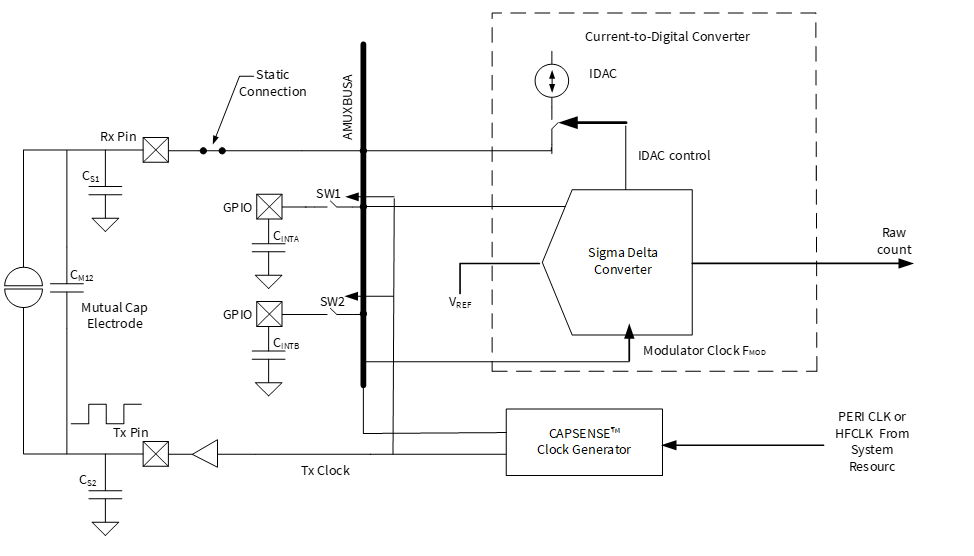
The CSX sensing method measures the mutual-capacitance between the Tx electrode and Rx electrode, as shown in
Figure 55
. The Tx electrode is excited by a digital waveform (Tx clock), which switches between
V
DDIO
(or
V
DDD
if
V
DDIO
is not available in the given part number) and ground. The Rx electrode is statically connected to AMUXBUS A. The CSX method requires two external integration capacitors,
C
INTA
and
C
INTB
. The value of these capacitors is listed in
Table 39
.
Figure 56. CSX sensing waveforms
shows the voltage waveforms on the Tx electrode and
C
INTA
and
C
INTB
capacitors. The sampling – a process of producing a “sample” – is started by the firmware by initializing the voltage on both external capacitors to
V
REF
and performing a series of sub-conversions. A sub-conversion is a capacitance to count conversions performed within a Tx clock cycle. The sum of results of all sub-conversions in a sample is referred to as “raw count”.
During a sub-conversion, both SW1 and SW2 switches are operated in phase with the Tx clock. On the rising edge of the Tx clock, SW1 is closed (SW2 is open during this time) and charge flows from the Tx electrode to the Rx electrode. This charge is integrated onto the
C
INTA
capacitor, which increases the voltage on C
INTA
. The IDAC is configured in sink mode to discharge the
C
INTA
capacitor back to voltage
V
REF
. On the falling edge of the Tx clock, SW2 is closed (SW1 is open during this time) and the charge flows from the Rx electrode to the Tx electrode. This causes the voltage on
C
INTB
to go below
V
REF
. The IDAC is configured in source mode to bring the voltage on
C
INTB
back to
V
REF
.
The charge transferred between Tx and Rx electrodes in both the cycles is proportional to mutual-capacitance,
C
M
, between the electrodes. The sigma delta converter controls IDAC for charging or discharging the external capacitors and also it measures the charging and discharging time in terms of modulator clock cycles for a sub-conversion. Multiple sub-conversions are performed during the CSX scanning and the result of each sub-conversion is accumulated to produce “raw count” for a sensor.
The modulator clock is used to measure the time taken to charge/discharge external capacitors within a Tx clock cycle. For this reason, modulator clock frequency must be always greater than Tx clock frequency; higher modulator clock frequency leads to better accuracy. For proper operation, the IDAC current should be set such that the
C
INTA
and
C
INTB
capacitors are charged/discharged within one Tx clock cycle. The CAPSENSE™ Component/middleware provides an option to automatically calibrate the IDAC. It is recommended to enable this option.
Figure 57. Raw count relationship for mutual-capacitance sensing
Where,
IDAC = IDAC current
C M
= Mutual-capacitance between Tx and Rx electrodes
V TX
= Amplitude of the Tx signal
F TX
= Tx clock frequency
F Mod
= Modulator clock frequency
N Sub
= Number of sub-conversions
When you place a finger on the CSX button, the mutual-capacitance between Rx and Tx electrodes decreases, which decreases the raw count. This decrease in raw count from the hardware is inverted by the CAPSENSE™ Component to make it similar to the raw count change in CSD for a finger touch. The final resulting inverted raw count is given by
Figure 58
.
Figure 58. Formula to determine rawcount
Component
See
CSX sensing method (third- and fourth-generation)
for more details of CSX hardware parameters.
CAPSENSE™ CSD-RM sensing method (fifth-generation and fifth-generation low-power)
This section provides an overview of the CSD-RM architecture implemented in the fifth-generation CAPSENSE™ device (known as multi sense converter (MSC)). The main features include ratiometric sensing, differential mode of operation without the need of reference voltage, use of capacitor DACs (CDAC) instead of current DACs (IDAC), which improves noise performance.
Figure 59. CAPSENSE™ CSD-RM (fifth-generation)
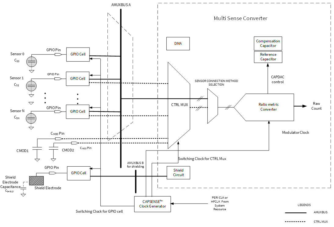
The fifth-generation low power (known as multi-sense low-power or MSCLP) technology has an internal clock removing the dependency on the system resource.
Autonomous scanning
is now enabled even without the CTRLMUX and DMA. All AMUXBUS CAPSENSE™ pins support autonomous scanning.
Figure 60. CAPSENSE™ CSD-RM (fifth-generation low-power)

GPIO cell capacitance to charge converter
GPIO cell capacitance to current converter
explains the GPIO cell configuration. In the fifth-generation architecture, the sensor is either interfaced to the AMUX (as before) or a new control MUX matrix, which supports autonomous scanning (limited number of pins supported). The GPIO cells are configured as switched-capacitance circuits that convert sensor capacitance into equivalent charge transfer.
Figure 61
shows the GPIO cell structure.
Figure 61. GPIO cell structure (fifth-generation)
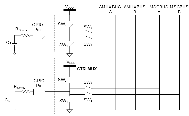
In the fifth-generation low-power architecture, the sensor is only interfaced to the AMUX, which now supports autonomous scanning (supports more number of pins than CTRLMUX).
Figure 62. GPIO cell structure (fifth-generation low-power)

Four non-overlapping, out-of-phase clocks of frequency
F SW
control the switches (SW1, SW2, SW3 and SW4) as
Figure 63
shows.
Figure 63. Voltage across sensor capacitance
Capacitor DACs (CDACs)
IDACs are replaced by CDACs in the fifth-generation CAPSENSE™ architecture. It consists of two CDACs, a reference capacitor DAC, and a compensation capacitor DAC. In each sense clock period, the sensor capacitance, as mentioned in
GPIO cell capacitance to charge converter
, transfers charge to both
C
MOD
s in such a way that it affects the voltage balance between the
C
MOD
s. Both capacitor DACs are switched on to
C
MOD
multiple times during a sense clock period to restore the voltage balance between the
C
MOD
s. The number of cycles required by the reference capacitor DAC to balance the voltage is proportional to the self-capacitance of the sensors.
The fifth-generation low-power CAPSENSE™ consists of Fine CDAC and Dither CDAC. The
Fine Reference CDAC (Cfine)
is a programmable CDAC, which is used to achieve finer resolution for the Reference CDAC. The
CDAC dither
is used to reduce
Flat-spots
(or dead zones).
CAPSENSE™ clock generator
This block generates the sense clock F
SW
, and the modulation clock F
MOD
, from the high-frequency system resource clock (HFCLK) or peripheral clock (PERI) depending on the PSOC™ device family.
Sense clock
Modulator clock
The modulation clock is used by the
Ratiometric sensing technology
. This clock determines the sensor scan time based on
Equation 16
and
Equation 17
.
Figure 64. Sensor scan time
Figure 65. Hardware scan time
Where,
Number of subconversions = Total number or sub-conversions in single scan
Subconversion = Capacitance to count conversions performed within a sense clock cycle
Sensor initialization time = Time taken by the sensor to write to the internal registers and initiate a scan
Ratiometric sensing technology
It consists of a ratiometric converter and two CDACs, a reference capacitor DAC, and a compensation capacitor DAC. In each sense clock period, the sensor capacitance, as mentioned in
GPIO cell capacitance to charge converter
, transfers charge to both
C
MOD
s
in such a way that it affects the voltage balance between the
C
MOD
s
. The ratiometric converter controls the reference CDAC by switching it ON or OFF corresponding to the small voltage variations across two
C
MOD
s
to maintain the
C
MOD
voltage at the same level. The number of cycles required by the reference capacitor DAC to balance the voltage between the
C
MOD
s
is proportional to the self-capacitance of the sensors.
The compensation capacitor is used to compensate excess mutual-capacitance from the sensor to increase the sensitivity. The number of times it is switched depends on the amount of charge the user application is trying to compensate (remove) from the sensor mutual capacitance.
The ratiometric converter can operate in either the single CDAC mode or dual CDAC mode.
In the single CDAC mode, the reference CDAC is controlled by the ratiometric converter; the compensation CDAC is always OFF
In the dual CDAC mode, the reference CDAC is controlled by the ratiometric converter; the compensation CDAC is always ON. The reference CDAC is capable of compensating up to 95%, results in the increased signal as explained in Conversion gain and CAPSENSE™ signal
In the single CDAC mode, if
C
REF
is the value of the reference CDAC, the approximate raw count value is given by
Equation 18
.
Figure 66. CSD-RM single CDAC raw count
In the dual CDAC mode, the compensation CDAC is always ON. If C
COMP
is the compensation CDAC, the raw count equation is given by
Equation 19
.
Figure 67. CSD-RM dual CDAC raw count
Where,
MaxCount =
N
Sub
.
SnsClk
Div
N Sub
= Number of sub-conversions
SnsClk Div
= Sense clock divider
CompClk Div
= Compensation CDAC divider
C S
= Sensor capacitance
C ref
= Reference capacitance
C comp
= Compensation capacitance
With CIC2 enabled,
Figure 68. Max raw count
Where,
Figure 69. Decimation rate
It is recommended to choose the number of CIC2 samples in such a way that "K" can be set to “1” to get the highest possible raw count.
Number of CIC2 samples | Recommended CIC2 shift for divider | CIC2 hardware divider |
|---|---|---|
2 | 1 | 2 |
3-4 | 2 | 4 |
5-8 | 3 | 8 |
9-16 | 4 | 16 |
17-32 | 5 | 32 |
33-64 | 6 | 64 |
65-128 | 7 | 128 |
129-256 | 8 | 256 |
Selecting the auto option for CIC2 shift in the CAPSENSE™ configurator selects hardware shift (hardware divider) as per
Table 4
.
The decimation rate is the down sampling rate, and when it reaches its maximum of 255, the following condition needs to be ensured to avoid CIC2 accumulator (25-bit) overflow.
Figure 70. CIC2 Accumulator overflow condition
Where,
CIC2_Acc_Size Max - Maximum CIC2 accumulator size
The maximum CIC2 accumulator size for a direct clock is (2
25
- 1), and for a PRS clock is (2
25
- 1)/2.
As per
Equation 18
, the output raw count is proportional to the ratio of sensor capacitance to the reference capacitance, and hence the name Ratiometric Sensing.
Noise improvement is one of the main advantages of the fifth-generation over previous generations of CAPSENSE™ technology. The dominant noise sources in the fourth-generation are current (I
MOD
), reference voltage (
V
REF
), and clock jitter (
F
SW
) (see
Figure 53
). These noise sources have been removed in the fifth-generation (see
Equation 19
). The IDAC has been replaced with CDAC. Since the system is now fully differential, it does not need
V
REF
. The CAPSENSE™ architecture is no longer affected by jitter as the scan result is now based on the edges of the clock rather than the duration of the clock. Because of differential architecture, the drift of raw count for a given power-supply ripple is significantly less in the fifth-gen and fifth-gen low-power CAPSENSE™. The user may not need any LDO to design with fifth-gen and fifth-gen low-power CAPSENSE™ technology if power supply ripple is within the limits mentioned in the datasheet.
Analog multiplexer (AMUX) and control matrix (CTRLMUX)
Another feature introduced in the Fifth-Generation is the control matrix (CTRLMUX) as shown in
Figure 59
. The CTRLMUX enables autonomous scanning and provides immunity to on-chip IO noise. The CTRLMUX allows the CAPSENSE™ IP to directly handle the sensor inputs
5
(in addition to the traditional GPIO mode), and hence supports autonomous scanning of the sensors without the CPU.
For fifth-generation low-power, as shown in the image
Figure 60
, the CTRLMUX has been removed. The AMUXBUS is enabled to handle autonomous scanning on all the CAPSENSE™ pins.
CAPSENSE™ CSDRM shielding
PSOC™ 4 CAPSENSE™ supports shield electrodes for liquid tolerance and proximity sensing. The purpose of the shielding is to remove the parasitic capacitance between the sensor and shield electrodes. See
Driven-shield signal and shield electrode
and
Effect of liquid droplets and liquid stream on a self-capacitance sensor
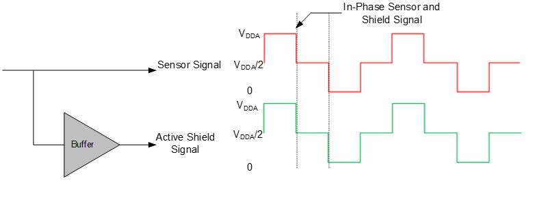
for details on how this is useful for liquid tolerance. The fifth-generation CAPSENSE™ architecture supports two shield modes – active and passive shielding.
Active shielding
In active shielding mode, the shield circuit drives the shield electrode with a replica of the sensor signal using a buffer as shown in
Figure 71
. This nullifies the potential difference between sensors and the shield electrode.
Figure 71. Active shield signal
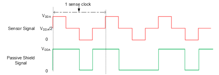
Passive shielding
In the passive shielding mode, there is no buffer used; instead, the shield is switched between
V
DDA
and GND as shown in
Figure 72
. The switching is controlled in such a way that the net charge between the sensor and the shield is nullified every two sense clocks.
Figure 72. Passive shield signal
provides the comparison of the active shielding features versus the passive shielding features.
Feature | Active shielding | Passive shielding | Effect |
|---|---|---|---|
Performance | Higher | Lower | Active shielding is preferred for high-performance applications. |
Power impact | Higher | Lower | Passive shielding is preferred for low-power applications. |
CAPSENSE™ CSX-RM sensing method (fifth-generation and fifth-generation low-power)
illustrates the CSX-RM sensing circuit. The implementation uses the following hardware subblocks:
Two 8-bit capacitor DACs and ratiometric converter
AMUXBUS and CTRLMUX
CAPSENSE™ clock generator for Tx clock and modulator clock
Port pins for Tx and Rx electrodes and external caps
Two external capacitors ( C MOD1 and CMOD2 )
Figure 73. CAPSENSE™ CSX-RM sensing method configuration (fifth-generation)
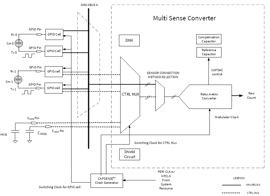
Figure 74. CAPSENSE™ CSX-RM sensing method configuration (fifth-generation low-power)

The CSX-RM sensing method measures the mutual-capacitance between the Tx electrode and Rx electrode, as shown in
Figure 73
. The Tx electrode is activated by a digital waveform (Tx clock), which switches between
V
DDA
and ground. The Rx electrode is statically connected to AMUXBUS A or CTRLMUX, as applicable. The CSX-RM method requires two external integration capacitors,
C
MOD1
and
C
MOD2
.
The sampling – a process of producing a “sample” – is started by the firmware by initializing the voltage on both external capacitors (
C
MOD
) to
V
DDA
/2 and performing a series of sub-conversions. A sub-conversion is a capacitance to count conversions performed within a Tx clock cycle. The sum of results of all sub-conversions in a sample is referred to as “raw count”.
On the rising and falling edge of the Tx clock, charge flows from the Tx electrode to the Rx electrode. In such a way that it unbalances the voltage between the external
C
MOD
capacitors. Both capacitor DACs (reference and compensation capacitor DACs) are switched onto
C
MOD
multiple times during a sense clock period to balance the
C
MOD
’s back to their original voltage. Number of cycles required by the reference capacitor DAC to balance is proportional to the mutual-capacitance,
C
m
, between the electrodes.
The number of times the reference capacitor is switched with respect to the modulator clock is denoted by the Tx clock divider value according to
Figure 75
.
Figure 75.
Tx clock divider
Where,
TxClk Div
= Tx clock divider
F Mod
= Modulator frequency
F Tx
= Tx clock frequency
The compensation capacitor is used to compensate excess mutual-capacitance from the sensor to increase the sensitivity. The number of times it is switched depends on the amount of charge the user application is trying to compensate (remove) from the sensor mutual-capacitance. The number of times the compensation capacitor is switched with respect to the modulator clock is denoted by the value of the compensation CDAC divider according to the
Equation 21
. The CDAC compensation clock divider must be less than or equal to the Tx clock divider.
Figure 76. Compensation CDAC divider
Where,
CompClk Div
= Compensation CDAC divider
FM MOD
= Modulator frequency
F comp
= Compensation CDAC clock frequency
Ratiometric sensing technology
The ratiometric converter gives an equivalent raw count which is proportional to the sensor mutual-capacitance after each scan. The ratiometric converter can operate in either single CDAC mode or dual CDAC mode.
In the single CDAC mode, the reference CDAC is controlled by the ratiometric converter; the compensation CDAC is always OFF
In the dual CDAC mode, the reference CDAC is controlled by the ratiometric converter; the compensation CDAC is always ON. Compensation CDAC is capable of compensating up to 95%, results in increased signal as explained in Conversion gain and CAPSENSE™ signal
In the single CDAC mode, if
C
ref
is the value of the reference CDAC, the approximate value of raw count is given by
Figure 77
.
Figure 77. CSX-RM single CDAC raw count
In the dual CDAC mode, the compensation CDAC is always ON. If C
comp
is the compensation CDAC, the equation for the raw count is given by
Figure 78
.
Figure 78. CSX-RM dual CDAC raw count
Where,
MaxCount = N
Sub
.TxClk
Div
N Sub
= Number of sub-conversions
SnsClk Div
= Sense clock divider
CompClk Div
= Compensation CDAC divider
C S
= Sensor capacitance
C ref
= Reference capacitance
C comp
= Compensation capacitance
With CIC2 enabled,
Figure 79. Max raw count
Where,
Figure 80. Decimation rate
It is recommended to choose the number of CIC2 samples in such a way that "K" can be set to “1” to get the highest possible raw count.
Number of CIC2 samples | Recommended CIC2 shift for divider | CIC2 hardware divider |
|---|---|---|
2 | 1 | 2 |
3-4 | 2 | 4 |
5-8 | 3 | 8 |
9-16 | 4 | 16 |
17-32 | 5 | 32 |
33-64 | 6 | 64 |
65-128 | 7 | 128 |
129-256 | 8 | 256 |
Selecting the auto option for CIC2 shift in the CAPSENSE™ configurator selects hardware shift (hardware divider) as per
Table 4
The decimation rate is the down sampling rate, and when it reaches its maximum of 255, the following condition needs to be ensured to avoid CIC2 accumulator (25-bit) overflow.
Figure 81. CIC2 Accumulator overflow condition
Where,
CIC2_Acc_Size
Max
- Maximum CIC2 accumulator size
The maximum CIC2 accumulator size for a direct clock is (2
25
- 1), and for a PRS clock is (2
25
- 1)/2.
According to
Figure 78
, the output raw count is proportional to the ratio of the mutual capacitance of the sensor to the reference capacitance, hence the name ratiometric sensing.
CAPSENSE™ multi-phase scanning method
CAPSENSE™ multi-phase scanning refers to a differential measurement of a target sensor's capacitance relative to other sensors, which is carried out by scanning multiple sensors at once. Typical applications include keypad matrix and touchscreens. This is useful for countering certain types of common-mode noise, like voltage ripples in the VDDA supply, which can turn into finger-injected noise in the system. Refer to Noise in CAPSENSE™ system for more details.
MPSC-D (Multi-phase self-cap differential)
MPSC-D is a technique for differential measurement of the target sensor capacitance. This is carried out by scanning multiple electrodes simultaneously.
In regular CSD scanning, there are four phases (ph0-ph3), and one electrode is scanned at a time in these phases. MPSC-D also uses four phases of scanning, but in contrast to CSD, multiple electrodes are scanned simultaneously instead of just one. The number of electrodes used for MPSC scanning is called the MPSC-D order and is referred to as 'N
MPSC-D
' or Multi-phase self order. The minimum supported value of N
MPSC-D
is 5. In other words MPSC-D is supported on the following:
Matrix buttons with at least 5 sensors
Touchpad with at least 5 row and 5 columns
Slider with at least 5 segments
Compared to a regular CSD scan, this technique allows for a decrease in scanning time with the same signal-to-noise ratio (SNR) or an increase in SNR if the scanning time remains the same. In the best-case scenario, the SNR increases by √N
MPSC-D
times if the scanning time remains constant.
Advantages
The MPSC-D technique offers several advantages over the regular CSD techniques:
Improved SNR:
MPSC-D technique provides a theoretical improvement in SNR by multiple of √N
MPSC-D
, where N
MPSC-D
is Multi-phase self-order.
Noise Reduction:
The MPSC-D technique described above helps in suppressing common mode noise, for example, white noise, LCD noise.
Shield Not Required:
There is no need to use a shield in MPSC-D.
Limitations of MPSC-D
Increased
power
consumption:
Enabling MPSC-D mode leads to higher power consumption because it involves simultaneously driving multiple electrodes instead of only one.
Additional
computing:
Multi-phase scanning techniques employ convolution and deconvolution methods that requires additional computing.
Note: Covering more than 50% of the sensors with a conductive object, may cause improper functioning of the MPSC-D widget.
Implementation of MPSC-D
The MPSC-D feature can be used with any CSD widget that has more than 5 sensing elements; MPSC is not supported for configurations with less than 5 electrodes. For example, to use MPSC-D, a CSD slider widget is added, as shown in the
Figure 82
, with a number of sensors greater than or equal to five.
Figure 82. Adding CSD Slider in CAPSENSE™ configurator
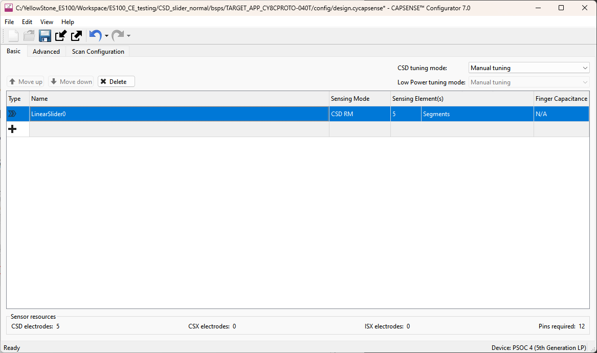
Each CSD widget with more than 5 sensing elements has a parameter called MPSC self-order. To access this parameter, open the Extra Parameters section in the Widget Details tab of the Advanced section.
Figure 83. Enabling MPSC-D in configuration
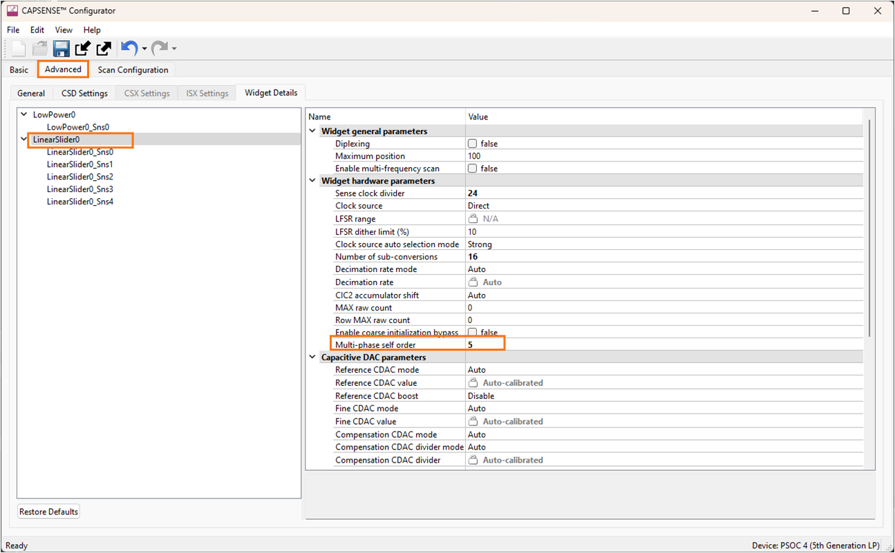
The number of electrodes involved during scanning defines the multi-phase selforder. The default value of multi-phase selforder is 1, which means MPSC-D is disabled. The multi-phase self-order can be set equal to the number of sensing elements. For example, if there are 5 sensing elements, the multi-phase self-order will be 5.
With multi-phase self-order set to the number of sensing elements of widget, the MPSC-D will be enabled by the system.
The table below presents a comparative analysis of power consumption, computation time, and Signal-to-Noise Ratio (SNR) for the
CY8CPROTO-040T kit
configured with a slider widget of 5 sensors with MPSC enabled and disabled.
Configuration used for the measurement:
Source clock = IMO 46 MHz
FMOD = 46 MHz
Tx Clock divider = 24
NSUB = 16
Parameters | With MPSC | Without MPSC |
|---|---|---|
SNR | 67.49 | 37.76 |
Power consumption (μA) | 151 | 120 |
Computation time (μs) | 94 | 53 |
Advantages of fifth generation and fifth generation low-power
See
AN234231 - Achieving lowest-power capacitive sensing with PSOC™ 4000T
for detailed information on autonomous scanning and the CIC2 filter.
Autonomous scanning
In previous generation CAPSENSE™ technology, after each scan, CPU is interrupted to configure the next sensor. Autonomous scanning mode in the fifth-generation CAPSENSE™ technology avoids the CPU intervention for scanning every subsequent sensor. This significantly reduces the CPU bandwidth required for scanning widgets with large number of sensors. Autonomous scanning requires features such as CTRLMUX and DMA. Since the number of pins supported with CTRLMUX is limited, the number of pins supporting autonomous scanning is also limited. See the
Configuring autonomous scan
section for more details.
In fifth-generation low-power CAPSENSE™, autonomous scanning is supported inherently, and requires neither CPU intervention nor CTRLMUX and DMA. All CAPSENSE™ pins support this scanning mode, via the AMUXBUS, compared to the limited number of pins, which were supported by the CTRLMUX in the fifth-generation CAPSENSE™ technology.
Usage of multiple channels
The PSOC™ 4100S Max device supports two fifth-generation CAPSENSE™ blocks – MSC0 and MSC1. Each block has the same functionality and performance as explained in the CAPSENSE™ CSD-RM sensing method(fifth-generation and fifth-generation low-power) and CAPSENSE™ CSX-RM sensing method(fifth-generation and fifth-generation low-power) sections. Each instance can be considered as a channel and multiple instances imply multiple channels. Multi-channel behavior can be supported by multiple instances in a single chip and/or having multiple chips. The operation of the channels is synchronized and operate in lockstep when scanning the sensors hooked in to the channels. Lockstep guarantees clock synchronization and avoids any cross-channel noise due to un-synchronized sense clocks.
See Multi-channel scanning section for more details.
CIC2
The multi-sense low-power (MSCLP) CAPSENSE™ device has a built-in cascaded integrator-comb 2 (CIC2) digital filter, which improves the effective resolution, and thereby the SNR, for a given scan period. The CIC2 filter is a 2
nd
order digital low-pass (decimation) filter used to filter delta-sigma converters.
Figure 84
shows the representation of a CIC2 filter made up of a cascade of two integrators and two comb filters.
The CIC2 filter receives the output of the MSCLP analog front end, which is a delta-sigma converter. This converter generates a bitstream of 1s and 0s representing its input, and moves the quantization noise to high frequencies. This high-frequency noise is filtered out by a digital low-pass filter; the downsampler converts the input to a single digital word representing the measured signal. This combination of a low-pass filter (A0, A1) and a downsampler (D0, D1) is known as a decimator (CIC2 filter) as shown in Figure 84 .
Figure 84. CIC2 filter block diagram

The raw count gets accumulated at the end of each valid sample.
A minimum of two valid CIC2 samples are required for proper CIC2 filtering. Considering two valid samples, calculate the decimation (down sampling) rate using the following equation:6)
Figure 85. Decimation rate
Configure the CIC2 Shift parameter as "Auto" in the CAPSENSE™ configurator. This automatically selects the appropriate hardware shift (hardware divider).
Calculate the max raw count, when CIC2 is enabled, using the following equation:
Figure 86. Max rawcount equation
CAPSENSE™ design and development tools
This section introduces the available software tools, such as PSOC™ Creator and ModusToolbox™, to develop your CAPSENSE™ application. For more details, see the user manual of the respective IDE.
Table 8
shows the supported devices and the CAPSENSE™ component/middleware version in PSOC™ Creator and ModusToolbox™.
Devices | Software tool | CAPSENSE™ library |
|---|---|---|
PSOC™ 4000S, PSOC™ 4100S, PSOC™ 4100S Plus, PSOC™ 4100S Plus 256K, PSOC™ 4500S | CAPSENSE™ middleware, CAPSENSE™ component | |
PSOC™ 4000T, PSOC™ 4100T Plus, PSOC™ 4100S Max, All PSOC™ 6 devices | ModusToolbox™ | CAPSENSE™ middleware |
All other PSOC™ 4 devices | PSOC™ Creator | CAPSENSE™ component |
PSOC™ Creator
PSOC™ Creator is a state-of-the-art, easy-to-use IDE. It offers a unique combination of hardware configuration and software development based on classical schematic entry. You can develop applications in a drag-and-drop design environment using a library of Components. For details, see the
PSOC™ Creator home page
.
CAPSENSE™ component
PSOC™ Creator provides a CAPSENSE™ component, which is used to create a capacitive touch system in PSOC™ by simply configuring this Component. The CAPSENSE™ component also provides an application programming interface (API) to simplify firmware development. Some PSOC™ 4 Bluetooth® LE and PSOC™ 6 MCU devices also support a CAPSENSE™ Gesture Component (see the corresponding
Device datasheet
to see if your device supports this Component).
Figure 87. PSOC™ Creator component placement
Each CAPSENSE™ component has an associated datasheet that explains details about the Component. To open the Component datasheet, right-click the Component and select
Open Datasheet
.
The CAPSENSE™ component also has a Tuner GUI, called the
Tuner GUI
, to help with the tuning process.
CapSense_ADC component
The CapSense_ADC
7
component is only applicable for the PSOC™ 4S-Series, PSOC™ 4100S Plus, PSOC™ 4100PS, and PSOC™ 6 MCU devices. This component should be used when both CAPSENSE™ and ADC operations are required. This component allows using the CAPSENSE™ block for ADC operation and touch functionality in a time-multiplexed manner.
Tuner GUI
Tuner helper is included with the
CAPSENSE™
component and assists in tuning CAPSENSE™ parameters and monitoring sensor data such as raw count, baseline, and difference count. Refer the
Component datasheet/middleware document
for the detailed procedure on how to use Tuner GUI.
Example projects
You can use the CAPSENSE™ example projects provided in PSOC™ Creator to learn schematic entry and firmware development. To find a CAPSENSE™ example project, go to the PSOC™ Creator home page, click
Find Code Example …
, and select the appropriate architecture, as
Figure 88
shows. You can also filter for a project by writing partial or complete project name in the
Filter by
field.
Figure 88. PSOC™ Creator example project
ModusToolbox™
ModusToolbox™ software suite is used for the development of PSOC™ 6 and PSOC™ 4
8
based CAPSENSE™ applications. You can download ModusToolbox™ from
here
. Before you start working with this software, it is recommended that you go through the
Quick start guide
and
user guide
. ModusToolbox™ software trainings can be found
here
. If you have ModusToolbox™ IDE installed in your system, you can create a CAPSENSE™ application for the devices supported in ModusToolbox™.
CAPSENSE™ middleware
ModusToolbox™ provides a CAPSENSE™ middleware, which can be used to create a capacitive touch system in PSOC™ by simply configuring parameters in the CAPSENSE™ configuration tool. The middleware also provides an application programming interface (APIs) to simplify firmware development. See the
CAPSENSE™ middleware library
for more details.
CAPSENSE™ configurator
The CAPSENSE™ configurator tool in
ModusToolbox™
is similar to that in
PSOC™ Creator
, which is used to configure the CAPSENSE™ hardware and software parameters. For more details on configuring CAPSENSE™ in ModusToolbox™, see the
ModusToolbox™ CAPSENSE™ configurator guide
and
CAPSENSE™ middleware library
.
Figure 89
shows how to open the CAPSENSE™ configuration tool in ModusToolbox™. Alternatively, it can also be opened from the
Quick panel
in the ModusToolbox™. For simplicity of documentation, this design guide shows selecting the CAPSENSE™ parameter in PSOC™ Creator CAPSENSE™ component.
Figure 89. CAPSENSE™ configurator tool in ModusToolbox™
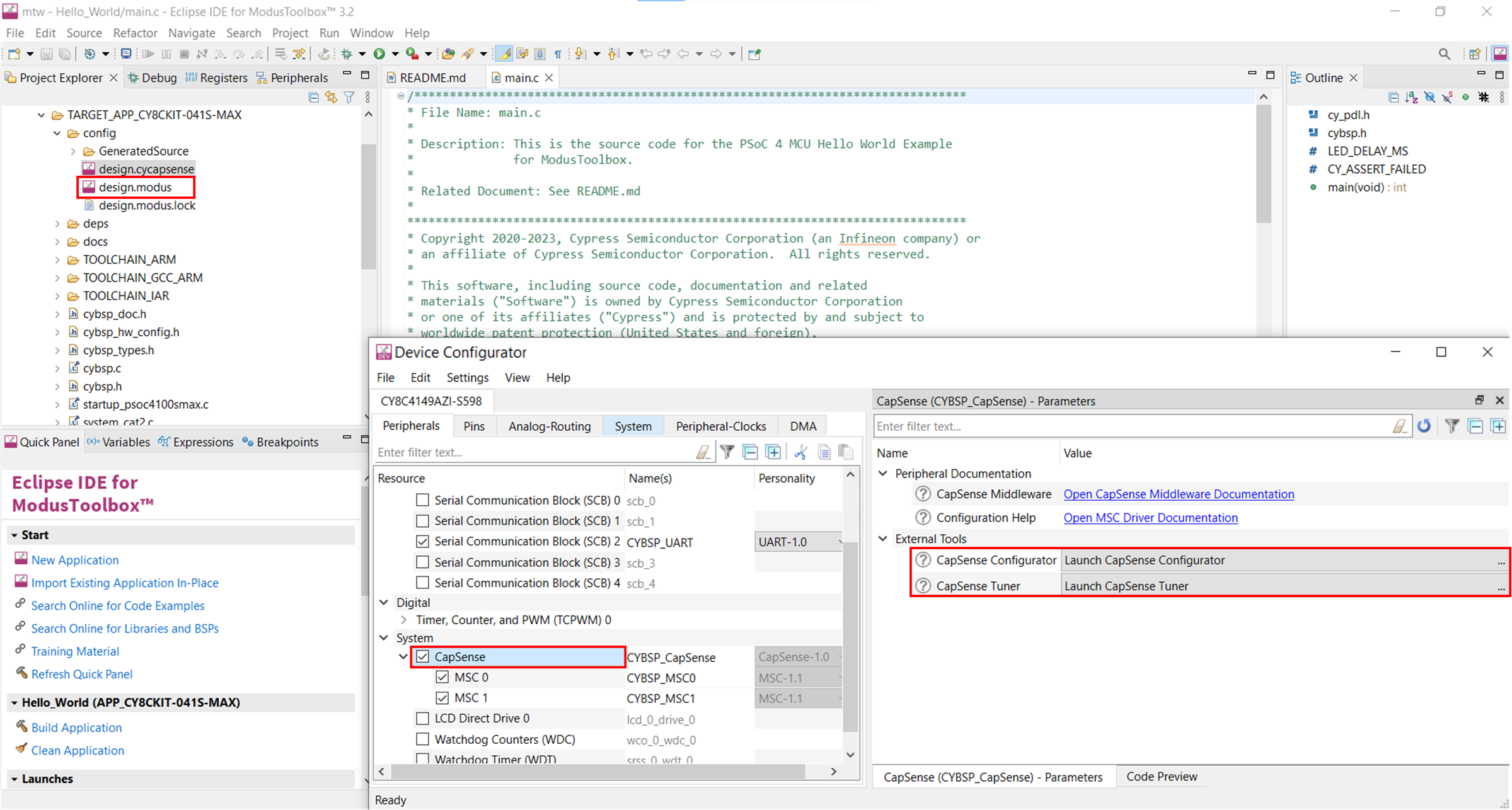
CSDADC middleware
This CSDADC middleware
9
should be used when both the CAPSENSE™ and ADC operations are required. This middleware allows using the CAPSENSE™ hardware block for ADC operation and touch functionality in a time-multiplexed manner. It could be used for all three sensing modes that is, CSD, ADC, and CSX. See the
CSDADC middleware library
documentation for more details.
CSDIDAC middleware
The CSDIDAC middleware allows you to use the CAPSENSE™ IDAC in a standalone mode. You can use this middleware if you are not using CAPSENSE™ middleware or if you are using only one IDAC for CAPSENSE™. See the
CSDADC middleware library
documentation.
CAPSENSE™ tuner
ModusToolbox™ also supports a GUI tool that can be used for tuning CAPSENSE™ parameters. This tool can be opened from the
Device configurator
by selecting Launch CAPSENSE™ tuner as shown in
Figure 89
. See the
CAPSENSE™ tuner guide
documentation.
Example projects
To quickly start the CAPSENSE™ system design, start with the example projects provided in ModusToolbox™. You can find a CAPSENSE™ example project by navigating to
. Choose the appropriate Board Support Package with a device.
Figure 90
shows creating a CAPSENSE™ CSD Button example starter code in ModusToolbox™ from the list of available code examples.
Figure 90. Creating CAPSENSE™ CSD Button example project in ModusToolbox™
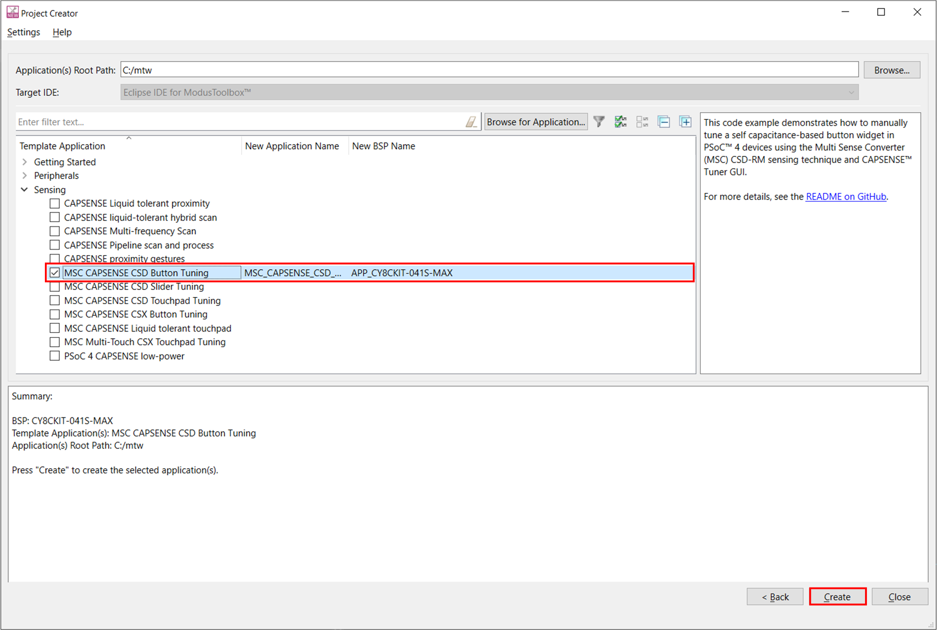
Hardware kits
lists the development kits that support evaluation of PSOC™ 4 and PSOC™ 6 CAPSENSE™.
Development kit | Supported CAPSENSE™ features |
|---|---|
PSOC™ 4000 pioneer kit ( CY8CKIT-040 ) | A 5x6 CAPSENSE™ touchpad and a wire proximity sensor |
PSOC™ 4 S-series pioneer kit ( CY8CKIT-041 ) | Two self- or mutual-capacitive sensing buttons A 7×7 self- or mutual-capacitive sensing touchpad |
PSOC™ 4 S-series prototyping kit ( CY8CKIT-145 ) | Three self- or mutual-capacitive sensing buttons A five-segment self- or mutual-capacitive sensing linear slider |
PSOC™ 4100S Plus prototyping kit ( CY8CKIT-149 ) | Three self- or mutual-capacitive sensing buttons A six-segment self- or mutual-capacitive sensing linear slider |
PSOC™ 4100S Max pioneer kit ( CY8CKIT041S-Max) | Two self- or mutual-capacitive sensing buttons An eight-segment self- or mutual-capacitive sensing linear slider A 10x16 self or mutual-capacitive sensing touchpad A proximity sensor loop |
PSOC™ 4000T kit ( CY8CKIT-040T ) | One CAPSENSE™ button A 4x5 self- or mutual-capacitive sensing touchpad A proximity sensor loop |
PSOC™ 4000T prototyping kit ( CY8CPROTO-040T ) | One self-capacitive sensing button One mutual-capacitive sensing button A proximity sensor loop A five-segment self- or mutual-capacitive sensing linear slider |
PSOC™ 4100T Plus prototyping kit ( CY8CPROTO-041TP ) | One self-capacitive sensing button One mutual-capacitive sensing button A proximity sensor loop A 4x5 self- or mutual-capacitive sensing touchpad |
PSOC™ 4 pioneer kit ( CY8CKIT042 ) | A five-segment linear slider |
PSOC™ 4 Bluetooth® LE pioneer Kit ( CY8CKIT-042-BLE ) | A five-segment linear slider and a wire proximity sensor |
PSOC™ 4200-M pioneer kit ( CY8CKIT-044 ) | A five-element gesture detection and two proximity wire sensors |
PSOC™ 4200-L pioneer kit ( CY8CKIT-046 ) | A five-element gesture detection, two proximity wire sensors, and an eight-element radial slider |
PSOC™ 4100PS prototyping kit ( CY8CKIT-147 ) | No onboard CAPSENSE™ sensors. The kit can be used to connect external sensors to any I/O pin. |
CAPSENSE™ proximity shield ( CY8CKIT-024 ) | A four-element gesture detection and one proximity loop sensor |
CAPSENSE™ liquid level sensing shield ( CY8CKIT-022 ) | A two-element flexible PCB and 12-element flexible PCB |
PSOC™ 4 processor module ( CY8CKIT038 ), with PSOC™ development kit ( CY8CKIT001 ) | A five-segment linear slider and two buttons |
CAPSENSE™ expansion board kit ( CY8CKIT-031 ), to be used with CY8CKIT038 and CY8CKIT-001 | A 10-segment slider, five buttons and a 4 x 4 matrix button with LED indication. |
MiniProg3 program and debug kit ( CY8CKIT-002 ) | CAPSENSE™ performance tuning in CY8CKIT-038 |
PSOC™ 6 Wi-Fi BT pioneer kit ( CY8CKIT-062-WiFi-BT pioneer kit ) and PSOC™ 6 Bluetooth® LE pioneer kit ( CY8CKIT062-BLE pioneer kit ) | A 5-segment CAPSENSE™ slider, two CAPSENSE™ buttons, one CAPSENSE™ proximity sensing header, a proximity sensor. |
PSOC™ 6 Wi-Fi BT prototyping kit ( CY8CPROTO-063-4343W ) | A 5-segment CAPSENSE™ slider and two mutual-cap CAPSENSE™ buttons |
CAPSENSE™ performance tuning
After you have completed the sensor layout (see
PCB layout guidelines
), the next step is to implement the firmware and tune the CAPSENSE™ parameters for the sensor to achieve optimum performance. The CAPSENSE™ sensing method is a combination of hardware and firmware techniques. Therefore, it has several hardware and firmware parameters required for proper operation. These parameters should be tuned to optimum values for reliable touch detection and fast response. Most of the capacitive touch solutions in the market must be manually tuned. A unique feature called SmartSense (also known as Auto-tuning) is available for PSOC™ 4 and PSOC™ 6 CAPSENSE™. SmartSense is a firmware algorithm that automatically sets all parameters to optimum values.
Selecting between SmartSense and manual tuning
SmartSense auto-tuning reduces design cycle time and provides stable performance across PCB variations, but requires additional RAM and CPU resources, as indicated in the
Component datasheet/middleware
document or
ModusToolbox™ CAPSENSE™ configurator guide
, to allow runtime tuning of CAPSENSE™ parameters. SmartSense is recommended mainly for conventional CAPSENSE™ applications involving simple button and slider widgets, and is currently supported only for
Self-capacitance sensing
and not
Mutual-capacitance sensing
.
On the other hand, manual tuning requires effort to tune optimum CAPSENSE™ parameters, but allows strict control over characteristics of capacitive sensing system, such as response time and power consumption. It also allows use of CAPSENSE™ beyond the conventional button and slider applications such as proximity and liquid-level-sensing.
SmartSense is the recommended tuning method for all the conventional CAPSENSE™ applications. You should use SmartSense auto-tuning if your design meets the following requirements:
The design is for conventional user-interface application like buttons, sliders, and touchpad
The parasitic capacitance ( C P ) of the sensors is within SmartSense-supported range as mentioned in the “SmartSense operating conditions” section in Component datasheet/middleware document or ModusToolbox™ CAPSENSE™ configurator guide
The sensor scan time chosen by SmartSense meets the response time/power requirements of the end system
SmartSense auto-tuning meets the RAM/flash requirements of the design
For all other applications, use
Manual tuning
. In such cases, you can also use SmartSense as an initial step to find the optimum hardware parameters such as Sense Clock frequency, and then change the tuning mode to manual tuning for further tuning of the CAPSENSE™ parameters. See
Using SmartSense to determine hardware parameters
.
Note: Manual tuning requires I2C or UART communication with a host PC.
SmartSense
Overview
The CAPSENSE™ algorithm is a combination of hardware and firmware blocks inside PSOC™. Therefore, it has several hardware and firmware parameters required for proper operation. These parameters need to be tuned to optimum values for reliable touch detection and fast response.
SmartSense is a CAPSENSE™ tuning method that automatically sets sensing parameters for optimal performance, based on user-specified finger capacitance values, and continuously compensates for system, manufacturing, and environmental changes.
Note: SmartSense currently supports widgets withCSD (Self-cap)Sensing mode only.CSX (Mutual-cap)widgets must be tuned manually.
Some advantages of SmartSense, as opposed to manual tuning are:
Reduced design cycle time:
The design flow for capacitive touch applications involves tuning all of the sensors. This step can be time consuming if there are many sensors in your design. In addition, you must repeat the tuning when there is a change in the design, PCB layout, or mechanical design. Auto-tuning solves these problems by setting all of the parameters automatically. Figure 91 shows the design flow for a typical CAPSENSE™ application with and without SmartSense
Figure 91. Design flow with and without SmartSense
Performance is independent of PCB variations:
The parasitic capacitance, C P , of individual sensors can vary due to process variations in PCB manufacturing, or vendor-to-vendor variation in a multi-sourced supply chain. If there is significant variation in C P across product batches, the CAPSENSE™ parameters must be re-tuned for each batch. SmartSense sets parameters for each device automatically, hence taking care of variations in CP
Ease of use:
SmartSense is faster and easier to use because only a basic knowledge of CAPSENSE™ is needed
Note that SmartSense can be used in multiple ways:
SmartSense (Full auto-tune) – This is the quickest way to tune. This method calibrates CAPSENSE™ hardware and software parameters automatically at runtime. This is the recommended method for most designs
SmartSense (Hardware parameters only) – This method auto-tunes all hardware parameters of CAPSENSE™, but allows to set user-defined threshold values (see Table 15 ). This method consumes less flash/RAM resources than SmartSense (Full Auto-Tune). Also, this method avoids the extra processing needed for automatic threshold calculation and hence allows lower power consumption for a given scan rate. Use this method for low-power or noisy designs or in cases with constrained memory requirements
SmartSense for initial tuning – You may also use SmartSense for initial tuning, to quickly find the best settings for a CAPSENSE™ board and then change to manual tuning. This method is useful for cases with strict requirements on response time or power consumption. This is a quick method to find the best settings, instead of starting manual tuning from scratch. Refer to the section Using SmartSense to determine hardware parameters for more details
Table 10. CAPSENSE™ parameters auto-tuned in SmartSense
Parameter
Full auto-tune mode
Hardware parameters only mode
Scan resolution
Calculated once on CAPSENSE™ initialization.
Compensation IDAC
Modulator IDAC
Sense clock frequency
Modulator clock frequency
Finger threshold
Calculated once on CAPSENSE™ initialization based on the selected finger capacitance and updated after each sensor scan.
Manual selection (see Table 15 ).
Noise threshold
Hysteresis
Negative noise threshold
Low baseline reset
SmartSense full auto-tune
In SmartSense Full Auto-tune mode, the only parameter that needs to be tuned by the user is the Finger Capacitance parameter. The Finger Capacitance parameter (
C
F
) indicates the minimum value of finger capacitance that should be detected as a valid touch by the CAPSENSE™ Component. Whenever the actual
C
F
that is added when the finger touches the button sensor is greater than the value specified for the Finger Capacitance parameter in the Component configuration window, the sensor status will change to ‘1’; however, if the actual C
F
added by the finger touch is less than the value specified in the Component configuration window, the sensor status will remain ‘0’. The way of tuning the finger capacitance is different for button and slider widgets.
Note: Even for SmartSense auto-tuning, the CAPSENSE™ Component allows manual configuration of some general parameters like enable/disable of compensation IDAC, filters, shield such as liquid-tolerance-related parameters and modulator clock. These can be left at their default values for most cases or configured based on the respective sections in this guide.
Tuning button widgets
This section explains how to choose the finger capacitance value for the button widget. You may perform only a coarse tuning of the Finger capacitance parameter for a working design, or you may choose to fine-tune the Finger capacitance value. Coarse-tuning will satisfy the requirements of most designs, but fine-tuning will allow you to choose the most efficient CAPSENSE™ parameters (that is, minimum sensor scan time) using SmartSense.
If you do not know the value of
C
F
(
C
F
can be estimated based on
Figure 6
), set the Finger capacitance as follows:
Start by specifying the highest value for finger capacitance (from the available options in the list) and check the SNR and button status when the button is touched. Use the Tuner GUI to find the SNR
Decrease the finger capacitance parameter value until the button status changes to ‘1’ on touch and SNR>5. Figure 92 shows the detailed steps to find the right value for the Finger capacitance parameter in your design
Enable filters if the SNR of one or more sensors is less than 5:1 when the set finger capacitance is already at the least finger capacitance supported in the Component. You can also enable filters if externally induced noise is causing a decrease in SNR. See
Table 11
to choose the right filter in this case. There are various types of filters available in the CAPSENSE™ Component such as Median Filter, IIR filter, and Average Filter; you can enable more than one filter to reduce the noise in the raw count according to the requirement.
If you choose to use an IIR filter, begin by selecting a filter with a higher value of the filter coefficient and keep decreasing it until you achieve an SNR greater than or equal to 5:1. Using filters will affect the response time. You must properly select the filter coefficient such that the response time and SNR requirement are satisfied.
If the SNR is still less than 5:1 even when the smallest allowed value of finger capacitance and proper filter is chosen, see
PCB layout
,
Manual tuning
, or
Tuning debug FAQs
for more details on debugging the issue.
Figure 92. Using SmartSense auto-tuning based CAPSENSE™ project in PSOC™ Creator
Filter | Description | Mathematical description | Application |
|---|---|---|---|
Median | Nonlinear filter that takes the three most recent samples and computes the median value. | Eliminates noise spikes from motors and switching power supplies | |
Average | Finite impulse response filter (no feedback) with equally weighted coefficients. It takes the four most recent samples and computes their average. | Eliminates periodic noise (for example, from power supplies) | |
First Order IIR | Infinite impulse response filter (feedback) with a step response similar to an RC low pass filter, thereby passing the low-frequency signals (finger touch responses). K value is fixed to 256. N is the IIR filter raw count coefficient. A lower N value results in lower noise, but slows down the response. | Eliminates high frequency noise. | |
Hardware IIR | Enables the hardware IIR filter (see the equation on the right) for regular widgets (except Proximity and Low Power). iirRCcoef – IIR filter raw count coefficient; valid range: 0 to 8. A low coefficient means lower filtering, while a higher coefficient means a higher response time. Note: There is no filtering for coefficient value “0”. | Eliminates high-frequency noise. |
Tuning slider widgets
For sliders, set finger capacitance to the highest value initially. Slide your finger on the slider. If at any position on the slider, at least one slider segment status is ON and has an SNR >5:1, and at least two slider segments report a “difference count” that is, a “sensor signal” value greater than 0, use this finger capacitance value. Otherwise, decrease the finger capacitance value until the above condition holds true.
Figure 93
shows how to tune the finger capacitance for slider widget.
If these conditions are not met even after setting minimum allowed Finger Capacitance, use
Manual tuning
or revise the hardware according to
Slider design
considerations or see
Tuning debug FAQs
.
Figure 93
explains the process of setting finger capacitance value for sliders.
Note: It is recommended to use the compensation IDAC because it allows a higher variation in the parasitic capacitance of the slider segment with respect to the slider segment that has the maximumCP.
Figure 93. Setting finger capacitance value for ssliders
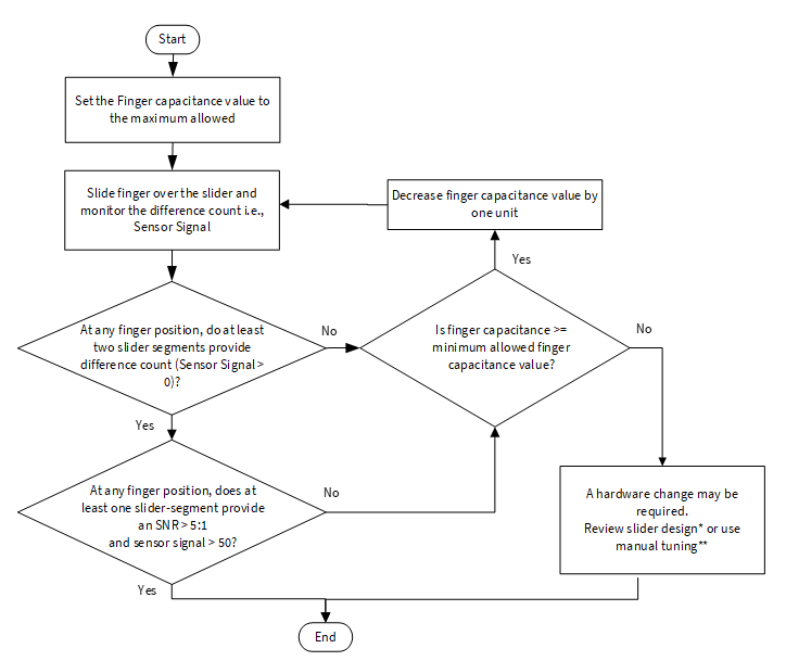
- To review slider design, see the Slider design section in the Design considerations chapter.
** To do manual tuning, see the Manual tuning section in the CAPSENSE™ performance tuning chapter.
Tuning proximity widgets
See
AN92239 Proximity sensing with CAPSENSE™
and the “Proximity sensing” section in
Getting started with CAPSENSE™ design guide
.
SmartSense hardware parameters-only mode
See
Table 15
for the recommended values for thresholds when the CSD tuning method is SmartSense (Hardware parameters only).
SmartSense for initial tuning
Manual tuning
Overview
SmartSense technology allows a device to calibrate itself for optimal performance and complete the entire tuning process automatically. This technology will meet the needs of most designs, but in cases where SmartSense does not work or there are specific SNR or power requirements, the CAPSENSE™ parameters can be adjusted to meet system requirements. This can be achieved by manual tuning.
Some advantages of manual tuning, as opposed to
SmartSense
auto-tuning are:
Strict control over parameter settings: SmartSense sets all the parameters automatically. However, there may be situations where you need to have strict control over the parameters. For example, use manual tuning if you need to strictly control the time PSOC™ takes to scan a group of sensors or strictly control the sense clock frequency of each sensor (this can be done to reduce EMI in systems)
Supports higher parasitic capacitances: If the parasitic capacitance is higher than the value supported by SmartSense, you should use manual tuning. See the Component datasheet/middleware document for more details on the supported range of parasitic capacitance by SmartSense
The manual tuning process can be summarized in the following three steps and is shown in
Figure 94
.
Set initial values of Selecting CAPSENSE™ hardware parameters using SmartSense (see Using SmartSense to determine hardware parameters ) or determine the values manually.
Tune CAPSENSE™ component hardware parameters to ensure that
Signal-to-noise
is greater than 5:1 with a signal of at least 50 counts while meeting the system timing requirements.
Set optimum values of Selecting CAPSENSE™ software parameters .
The following sections describe the fundamentals of manual tuning and the above three steps in detail. Knowledge of the CAPSENSE™ architecture in PSOC™ is a prerequisite for these sections. See Capacitive touch sensing method and CAPSENSE™ generations in PSOC™ 4 and PSOC™ 6 . The main difference in CAPSENSE™ architecture across different generations are listed in Table 2 .
Depending upon the sensing method selected, the manual tuning procedure will differ. See CSD sensing method (third- and fourth-generation) , CSX sensing method (third- and fourth-generation) chapter for their respective manual tuning procedures. You can skip these sections if you are not planning to use manual tuning in your design.
Figure 94
shows a general manual tuning procedure.
Figure 94. Manual tuning process overview
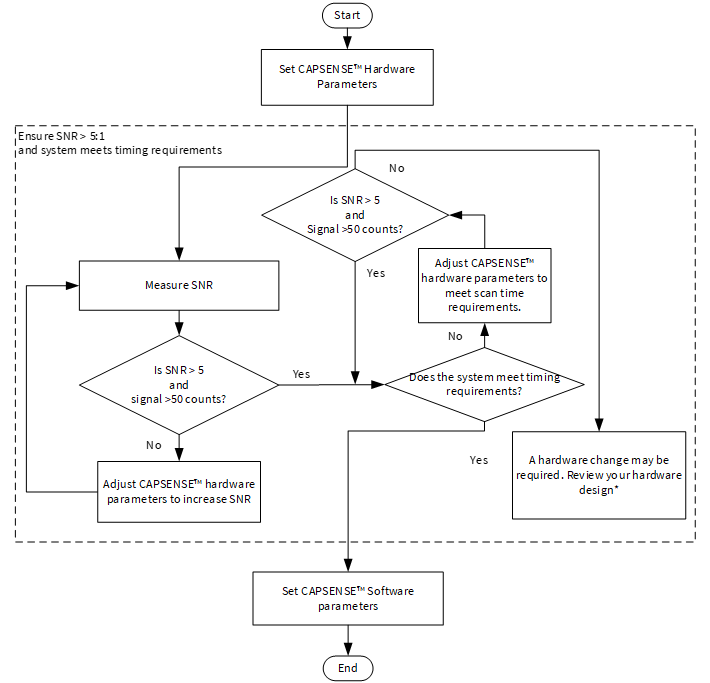
- To review the hardware design, see the Sensor construction and PCB layout guidelines sections in the Design considerations chapter.
CSD sensing method (third- and fourth-generation)
This section explains the basics of manual tuning using CSD sensing method. It also explains the hardware and software parameters that influence CSD sensing method and procedure of manual tuning for button, slider, touchpad and proximity widgets.
Basics
Conversion gain and CAPSENSE™ signal
Conversion gain will influence how much signal the system sees for a finger touch on the sensor. If there is more gain, the signal is higher, and a higher signal means a higher achievable
Signal-to-noise ratio (SNR)
.
Note: An increased gain may result in an increase in both signal and noise. However, if required, you can use firmware filters to decrease noise. For details on available firmware filters, seeTable 11.
Conversion gain in single IDAC mode
In the single IDAC mode, the raw count is directly proportional to the sensor capacitance.
Figure 95. Raw count relationship to sensor capacitance
Where,
C S
= sensor capacitance
CS
=
C
P
if there is no finger present on sensor
C S
= (
C
P
+
C
F
) when there is a finger present on the sensor
G CSD
= Capacitance to digital conversion gain of CAPSENSE™ CSD
The approximate value of this conversion gain using the IDAC sourcing mode, according to
Figure 51
and
Figure 95
is:
Figure 96. Capacitance to digital converter gain
Figure 97. Capacitance to digital converter gain (sinking IDAC mode)
Where,
V REF
= Comparator reference voltage. Refer
Table 2
.
F SW
= Sense clock frequency
I MOD
= Modulator IDAC current
N = Resolution of the sigma to delta converter.
The tunable parameters of the conversion gain are
V
REF
,
F
SW
, I
MOD,
and N.
Figure 98
illustrates a plot of raw count versus sensor capacitance.
Figure 98. Raw count versus sensor capacitance
The change in raw counts when a finger is placed on the sensor is called CAPSENSE™ signal.
Figure 99
shows how the value of the signal changes with respect to the conversion gain.
Figure 99. Signal values for different conversion gains
shows three plots corresponding to three conversion gain values
G
CSD3
,
G
CSD2
,and
G
CSD1
. An increase in the conversion gain results in higher signal value. However, this increase in the conversion gain also moves the raw count corresponding to
C
P
(that is, Baseline) towards the maximum value of raw count (2
N
-1). For very high gain values, the raw count saturates as the plot of
G
CSD3
shows. Therefore, you should tune the conversion gain to get a good signal value while avoiding saturation of raw count. Tune the CSD parameters such that when there is no finger on the sensor, that is when
C
S
=
C
P
, the raw count = 85% of (2
N
-1) as
Figure 100
shows. This ensures maximum gain, with enough margin for the raw count to grow because of environmental changes, and not saturate on finger touches.
Figure 100. Recommended tuning
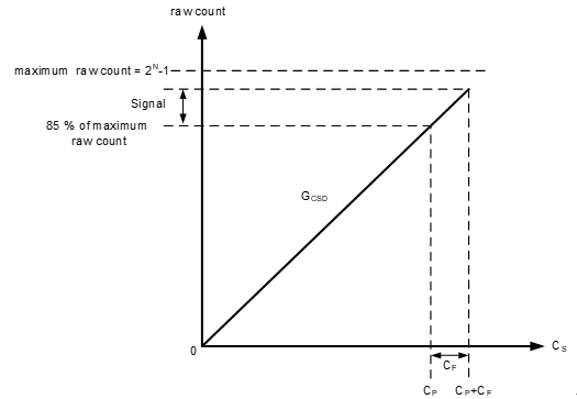
Conversion gain in dual IDAC mode
The equation for raw count in the
dual IDAC mode
, according to
Figure 95
and
Figure 53
is:
Figure 101. Dual IDAC mode raw counts
Where,
I COMP
= Compensation IDAC current
G CSD
is given by
Figure 50
for sourcing IDAC mode and
Figure 97
for sinking IDAC mode.
In both single IDAC and dual IDAC mode, tune the CSD parameters, so that when there is no finger on the sensor,that is when C
S
= ,
C
P
the raw count = 85% of (2N-1), as
Figure 102
shows, to ensure high conversion gain, to avoid
Flat-spots
, and to avoid raw count saturation due to environmental changes.
Figure 102. Recommended tuning in dual IDAC mode
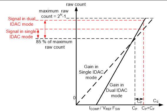
As
Figure 102
shows, the 85% requirement restricts to a fixed gain in single-IDAC mode, while in dual-IDAC mode, gain can be increased by moving the CS axis intercept to the right (by increasing ICOMP ) and correspondingly decreasing the modulator IDAC (
IMOD
) to still achieve raw count = 85% of (2
N
-1) for
C
S
=
C
P
. Using dual IDAC mode this way brings the following changes to the Raw Count versus
C
P
graph:
Use of compensation IDAC introduces a non-zero intercept on the C S axis as given in .
Figure 103. CS axis intercept with regards to I COMP
The value of
I
MOD
in the dual IDAC mode is half compared to the value of
I
MOD
in the single IDAC mode (all other parameters remaining the same), so the gain GCSD in the dual IDAC mode is double the gain in the single IDAC mode according to
dual IDAC mode
. Thus, the signal in the dual IDAC mode is double the signal in the single IDAC mode for a given resolution N.
While manually tuning a sensor, keep
dual IDAC mode
and
Figure 77
as well as the following points in mind:
Higher gain leads to increased sensitivity and better overall system performance. However, do not set the gain such that raw counts saturate, as the plot of gain G CSD3 shows in Figure 99 . It is recommended to set the gain in such a way that the raw count corresponding to CP is 85 percent of the maximum raw count for both the single IDAC and dual IDAC mode. The sense clock frequency ( FSW ) should be set carefully; higher the frequency, higher the gain, but the frequency needs to be low enough to fully charge and discharge the sensor as Figure 77 indicates
Enabling the Compensation IDAC plays a huge role in increasing the gain; it will double the gain if set as recommended above. Always enable the Compensation IDAC when it is not being used for general-purpose applications
Lower the modulation IDAC current, higher the gain. Adjust your IDAC to achieve the highest gain, but make sure that the raw counts corresponding to CP have enough margin for environmental changes such as temperature shifts, as indicated in Figure 100 and Figure 102
Increasing the number of bits of resolution used for scanning increases gain. An increase in resolution by one bit will double the gain of the system, but also double the scan time according to Figure 49 . A balance of scan time and gain needs to be achieved using resolution
Flat-spots
Ideally, raw counts should have a linear relationship with sensor capacitance as
Figure 98
and
Figure 102
show. However, in practice, sigma delta modulators have non-sensitivity zones, also called flat-spots or dead-zones – for a range of sensor capacitance values, the sigma delta modulator may produce the same raw count value as Figure 104 shows. This range is known as a dead-zone or a flat-spot.
Figure 104. Flat-spots in raw counts versus sensor capacitance when direct clock is used

In the case of CAPSENSE™ CSD, these flat spots occur near 25, 50, and 75 percent of the maximum raw count value (that is, near 25%, 50%, and 75% of 2
N
-1, where N =
Scan resolution
). These flat spots are prominent when direct clock is used as
Sense clock
source. Flat-spots do not occur if PRS is used as the Sense Clock source (see also section
Using SmartSense to determine hardware parameters
.
For almost all systems, we recommend using PRS as the Sense Clock source because it limits the impact of flat spots and also provides EMI/EMC benefits as indicated in
Sense clock
. If your system requires a direct clock, ensure that you use
auto-calibration
or avoid this raw count range when using manual calibration.
Flat-spots reduction techniques
Calibrate rawcount to 85%
In the case of CAPSENSE™ CSD, these flat-spots occur near 25, 50, and 75 percent of the maximum raw count value (that is, near 25%, 50%, and 75% of 2N-1, where ‘N’ is the scan resolution). Setting calibration to 85% decreases the width of flat-spots significantly.
Use PRS clock
These flat-spots are prominent when direct clock is used as the
Sense clock
source. Flat-spots do not occur if PRS is used as the Sense Clock source (refer to the
Using SmartSense to determine hardware parameters
section). For almost all systems, we recommend using PRS as the Sense Clock source because it limits the impact of flat-spots and also provides EMI/EMC benefits as indicated in
Sense clock source
. If your system requires a direct clock, ensure that you use
auto-calibration
or avoid this raw count range when using manual calibration.
Selecting CAPSENSE™ hardware parameters
CAPSENSE™ hardware parameters govern the conversion gain and CAPSENSE™ signal.
Table 12
lists the CAPSENSE™ hardware parameters that apply to CSD sensing method. The following subsection gives guidance on how to adjust these parameters to achieve optimal performance for CAPSENSE™ CSD system.
For simplicity of documentation, this design guide shows selecting the CAPSENSE™ parameters in PSOC™ Creator. You can use the same procedure to set the parameters in ModusToolbox™. However, in ModusToolbox™, you set the Sense clock and Modulator clock using divider values while in the PSOC™ Creator you specify the frequency value directly in the configurator. For more details on configuring CAPSENSE™, see the
Component datasheet/middleware
document.
Sl. No. | CAPSENSE™ parameter in PSOC™ Creator | CAPSENSE™ parameter in ModusToolbox™ |
|---|---|---|
1 | Sense cock frequency | Sense clock divider |
2 | Sense clock source | Sense clock source |
3 | Modulator clock frequency | Modulator clock divider |
4 | Modulator IDAC | Modulator IDAC |
5 | Compensation IDAC | Compensation IDAC |
6 | Scan resolution | Scan resolution |
Using SmartSense to determine hardware parameters
Parameters listed in
Table 12
are CAPSENSE™ hardware parameters. Tuning these parameters manually for optimal value is a time-consuming task. You can use SmartSense to determine these hardware parameters and take it as an initial value for manual tuning. You can fine-tune these values to further optimize the scan time, SNR, power consumption, or improving EMI/EMC capability of the CAPSENSE™ system.
Set the tuning mode to SmartSense and configure default values for parameters other than finger capacitance. See the
SmartSense
section for the tuning procedure and use the Tuner GUI to read back all the hardware parameters set by SmartSense. See the
Component datasheet/middleware document
for more details on how to use the Tuner GUI.
shows the best hardware parameter values in the Tuner GUI that are tuned by SmartSense for a specific hardware to sense a minimum finger capacitance of 0.1 pF.
Figure 105. Read-back hardware parameter values in Tuner GUI
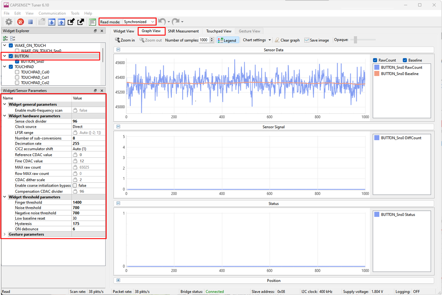
Manually tuning hardware parameters
Sense clock parameters
There are two parameters that are related to Sense clock: Sense clock source and Sense clock frequency.
Sense clock source
Select “Auto” to let the Component automatically choose the best sense clock source from Direct, PRSx, and SSCx for each widget. If not selecting Auto, then select the clock source based on the following:
Use pseudo random sequence (PRSx) modes to remove flat-spots
Use spread spectrum clock (SSCx) modes for reducing EMI/EMC noise at a particular frequency. This feature is available in the PSOC™ 4 S-Series, PSOC™ 4100S Plus, PSOC™ 4100PS, and PSOC™ 6 family of devices. In this case, the frequency of the sense clock is spread over a predetermined range
Use the direct clock for absolute capacitance measurement
When selecting PRSx as the sense clock source, ensure that the sequence completes within one conversion cycle; not letting the sequence complete may cause high noise in raw count, that is,
T
PRS
<<
T
SCAN
.
For PRS clock, use the following equations to calculate one PRS sequence completion cycle and scan time.
Figure 106. Sensor scan time
Figure 107. PRS sequence period
See the
Component datasheet/middleware document
for more details on the rules and recommendations for SSCx selection.
Sense clock frequency
The sense clock frequency should be selected so that the sensor will charge and discharge completely in each sense clock period as
Figure 44
shows.
This requires that the maximum sense clock frequency be chosen per
Figure 108
.
Figure 108. Sense clock maximum frequency
Figure 109. Total series resistance
Here,
C
P
is the sensor parasitic capacitance, and R
SeriesTotal
is the total series-resistance, including the 500 Ω resistance of the internal switches, the recommended external series resistance of 560 Ω (connected on PCB trace connecting sensor pad to the device pin), and trace resistance if using highly resistive materials (example ITO or conductive ink);that is, a total of 1.06 kΩ plus the trace resistance.
The value for CP can be estimated using the CSD Built-in-Self-test API;
GetSensorCapacitance()
. See the
Component datasheet/middleware document
for details.
shows that it is best to use the maximum clock frequency to have a good gain; however, you should ensure that the sensor capacitor fully charges and discharges as shown in
Figure 44
.
Generally, the
C
P
of the shield electrode will be higher compared to sensor
C
P
. For good liquid tolerance, the shield signal should satisfy the condition mentioned in
Shield electrode tuning theory
. If it is not satisfied, reduce the sense clock frequency further to satisfy the condition.
Modulator clock frequency
The modulator clock governs the conversion time for capacitance-to-digital conversion, also called the “sensor scan time” (see
Figure 49
).
A lower modulator clock frequency implies the following:
Longer conversion time (see
Figure 77
and
Figure 75
)
Lower peak-to-peak noise on raw count because of longer integration time of the sigma-delta converter
Wider Flat-spots
Select the highest frequency for the shortest conversion time and narrower flat spots for most cases. Use slower modulator clock to reduce peak-to-peak noise in raw counts if required.
Modulation and compensation IDACs
CSD supports two IDACs: Modulation IDAC and Compensation IDAC that charge
C
MOD
as
Figure 39
shows. These govern the
Conversion gain in dual IDAC mode
for capacitance-to-digital conversion. The CAPSENSE™ Component allows the following configurations of the IDACs:
Enabling or disabling of Compensation IDAC
Enabling or disabling of Auto-calibration for the IDACs
DAC code selection for Modulator and Compensation IDACs if auto-calibration is disabled
Compensation IDAC
Enabling the compensation IDAC is called “dual IDAC” mode, and results in increased signal as explained in
Conversion gain in dual IDAC mode
. Enable the compensation IDAC for most cases. Disable the compensation IDAC only if you want to free the IDAC for other general-purpose analog functions.
Auto-calibration
This feature enables the firmware to automatically calibrate the IDAC to achieve the required calibration target of 85%. It is recommended to enable auto-calibration for most cases. Enabling this feature will result in the following:
Fixed raw count calibration to 85% of maximum raw count even with part-to-part CP variation
Avoids Flat-spots
Automatically selects the optimum gain
If your design environment includes large temperature variation, you may find that the 85% IDAC calibration level is too high, and that the raw counts saturate easily over large changes in temperature, leading to lower SNR. If this is the case, you can adjust the calibration level lower by using
CapSense_CSDCalibrateWidget()
in your firmware.
For proper functioning of CAPSENSE™ under diverse environmental conditions, it is recommended to avoid very low or high IDAC codes. For a 7-bit IDAC, it is recommended to use IDAC codes between 18-110 from the possible 0 to 127 range. You can use CAPSENSE™ tuner to confirm that the auto-calibrated IDAC values fall in this recommended range. If the IDAC values are out of the recommended range, based on
Figure 95
,
Figure 96
and
Figure 101
, you may change the
V
Ref
or
F
SW
to get the IDAC code in proper range.
Disable IDAC auto-calibration if a change in
C
P
needs to be detected by measuring the raw count level at reset, for example:
Detecting large variations in sensor C P across boards or layout problems
Detecting finger touch at reset
Advanced CAPSENSE™ methods like liquid-level sensing, for example, to have different raw count level for different liquid levels at reset
Selecting DAC codes
This is not the recommended approach. However, this could be used only If you want to disable auto-calibration for any reason. To get the IDAC code, you may first configure CAPSENSE™ Component with auto-calibration enabled and all other hardware parameters the same as required for final tuning and read back the calibrated IDAC values using
Tuner GUI
. Then, re-configure the CAPSENSE™ Component to disable auto-calibration and use the obtained IDAC codes as fixed DAC codes read-back from the
Tuner GUI
.
Scan resolution
It governs the sensor scan time per Figure 106 and the conversion gain per
Figure 95
,
Figure 96
, and
Figure 101
. Scan resolution needs to be selected to maintain a balance between the signal and scan time.
Higher scan resolution implies the following:
Longer scan time per Figure 106
Higher SNR on raw counts (increase in resolution increases the signal at a disproportionate rate to noise)
In general, it is recommended to tune the resolution to achieve as high SNR as possible; however if the system is constrained on power consumption and/or response time, set the lowest resolution to achieve at-least 5:1 SNR in the end system.
Note: You should tune the scan resolution for less than 10:1 SNR only if you have scan time or power number constraints.
Tuning shield electrode
The shield related parameters need to be additionally configured or tuned differently when you enable the Shield electrode in the CSD sensing method for liquid tolerance or reducing the
C
p
of the sensor.
Shield electrode tuning theory
Ideally, the shield waveform should be exactly the same as that of the sensor as explained in
Driven shield signal and shield electrode
. However, in practical applications, the shield waveform may have a higher settling time and an overshoot error. Observe the sensor and shield waveform in the oscilloscope; an example waveform is shown in
Driven shield signal and shield electrode
. The shield waveform should settle to the sensor voltage within 90% of ON time of the sense clock waveform and the overshoot error of the shield signal with respect to
V
REF
should be less than 10%.
If these conditions are not satisfied, you will observe a change in raw count of the sensors when touching the shield hatch; in addition, if inactive sensors are connected to shield as mentioned in
Inactive sensor connection
, touching one sensor can cause change in raw count on other sensors, which indicates that there is cross talk if the shield electrode is not tuned properly.
In SmartSense, the sense clock frequency is automatically set. Check if these conditions are satisfied. If not satisfied, switch to
Manual tuning
and set the Sense clock frequency manually so that these conditions are satisfied. You can also tune the
Shield SW resistance
parameter to reduce the overshoot error.
Figure 110. Properly tuned shield waveform
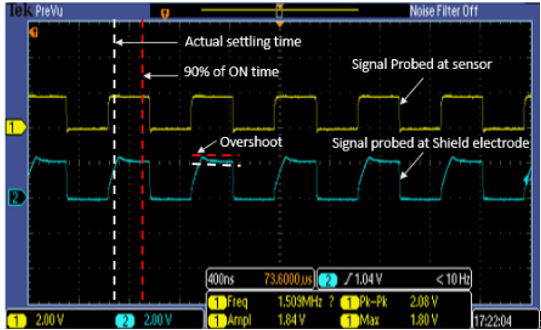
Tuning shield-related parameters
Enable shield tank capacitor
Enabling a shield tank capacitor increases the drive strength of the shield thus allowing the shield signal to settle to the sensor voltage faster as required. It is recommended to use the shield tank capacitor for PSOC™ 4A-S and PSOC™ 6 MCU family of devices. For PSOC™ 4A, PSOC™ 4A-L, and PSOC™ 4A-M family of devices, the shield tank capacitor does not prove very advantageous because it doubles the shield series resistance. It is recommended to keep this option disabled for these device families.
Shield electrode delay
For proper operation of the shield electrode, the shield signal should match the sensor signal in phase. Due to the difference in trace lengths of the sensor and shield electrodes, the shield waveform may arrive earlier to the sensor waveform. You can use an oscilloscope to view both sensor and shield signals to verify this condition. If they are not aligned, use this option to add delay to the shield signal to align the two signals. Available delays vary depending on the device selected.
Shield SW resistance
This parameter controls the shield signal rise and fall times to reduce EMI. This parameter is valid only for PSOC™ 4 S-Series, PSOC™ 4100S Plus, PSOC™ 4100PS, and PSOC™ 6 MCU family of devices. The default value of shield switch resistance is Medium.
Table 13
shows the effect of the Shield SW resistance value. You should select this value based on the application requirement; in addition, ensure that it satisfies the conditions in
Shield electrode tuning theory
.
Lower switch resistance | Higher switch resistance |
|---|---|
Large overshoot error Higher electromagnetic emission Faster settling time that is, higher maximum sense clock frequency | Smaller overshoot error Lower electromagnetic emission Slower settling time that is, lower maximum sense clock frequency |
Number of shield electrodes
This parameter specifies the number of shield electrodes required in the design. Most designs work with one dedicated shield electrode; however, some designs require multiple dedicated shield electrodes for ease of PCB layout routing or to minimize the PCB real estate used for the shield layer. See
Layout guidelines for shield electrode
.
Inactive sensor connection
When the shield electrode is enabled for liquid-tolerant designs, or if you want to use shield to reduce the sensor parasitic capacitance, this option should be specified as “Shield”; otherwise, select “Ground”.
However, there is a risk of higher radiated emission due to inactive sensors getting connected to Shield. In such situations, use the CAPSENSE™ API to manually control inactive sensor connections. Instead of connecting all unused sensors to the shield, connect only the opposing inactive sensors or inactive sensors closer to the sensor being scanned to shield for reducing the radiated emission.
Selecting CAPSENSE™ software parameters
CAPSENSE™ software parameters govern the sensor status based on the raw count of a sensor.
Table 14
provides a list of CAPSENSE™ software parameters. These parameters apply to both CSD and CSX sensing methods. This section defines these parameters with the help of
Baseline
, and provides guidance on how to adjust these parameters for optimal performance of your design.
Table 15
shows the recommended values for the software threshold parameter and they are applicable for most of the designs. However, if there are any external noise present in the end system, you must modify these thresholds accordingly to avoid any sensor false trigger.
Sl. No. | CAPSENSE™ component parameter name in PSOC™ Creator/ModusToolbox™ |
|---|---|
Finger threshold | |
Noise threshold | |
Hysteresis | |
ON debounce | |
Sensor auto-reset | |
Low baseline reset | |
Negative noise threshold |
Sl. No. | CAPSENSE™ threshold parameter | Recommended value |
|---|---|---|
Finger threshold | 80 percent of signal | |
Noise threshold | 40 percent of signal | |
Hysteresis | 10 percent of signal | |
ON debounce | 3 | |
Low baseline reset | 30 | |
Negative noise threshold | 40 percent of signal |
Baseline
After tuning the CAPSENSE™ Component for a given C
P
, the raw count value of a sensor may vary gradually due to changes in the environment such as temperature and humidity. Therefore, the CAPSENSE™ Component creates a new count value known as baseline by low-pass filtering the raw counts.
Baseline
keeps track of, and compensates for, the gradual changes in raw count. The baseline is less sensitive to sudden changes in the raw count caused by a touch. Therefore, the baseline value provides a reference level for computing signal.
shows the concept of raw count, baseline, and signal.
Figure 111. Raw count, baseline, and signal
Baseline update algorithm
To properly tune the CAPSENSE™ software, that is, the threshold parameters, it is important to understand how baseline is calculated and how the threshold parameters affect the baseline update.
Baseline is a low-pass-filtered version of raw counts. As
Figure 112
shows, baseline is updated by low-pass-filtering raw counts if the current raw count is within a range of (
Baseline –
Negative noise threshold
) to (
Baseline +
Noise threshold
). If the current raw count is higher than baseline by a value greater than noise threshold, baseline remains at a constant value equal to prior baseline value.
Figure 112. Baseline update algorithm
If the current raw count is below baseline minus negative noise threshold, baseline again remains constant at a value equal to prior baseline value for
Low baseline reset
number of sensor scans. If the raw count continuously remains lower than baseline minus noise threshold for low baseline reset number of scans, the baseline is reset to the current raw count value and starts getting updated again, as
Figure 113
shows.
Figure 113. Low baseline reset
Finger threshold
The finger threshold parameter is used along with the hysteresis parameter to determine the sensor state, as
Figure 114
shows.
Figure 114. Sensor state
Note: Signal in the above equation refers to the difference: raw count – baseline, when the sensor is touched, asFigure 111shows.
It is recommended to set finger threshold to 80 percent of the signal. This setting allows enough margin to reliably detect sensor ON/OFF status over signal variations across multiple PCBs.
Hysteresis
The hysteresis parameter is used along with the finger threshold parameter to determine the sensor state, as
Figure 114
and
Figure 115
show. Hysteresis provides immunity against noisy transitions of sensor state. The hysteresis parameter setting must be lower than the finger threshold parameter setting. It is recommended to set hysteresis to 10 percent of the signal.
Figure 115. Hysteresis
Noise threshold
For single-sensor widgets, such as buttons and proximity sensors, the noise threshold parameter sets the raw count limit above which the baseline is not updated, as
Figure 112
shows. In other words, the baseline remains constant as long as the raw count is above
baseline + noise threshold
. This prevents the baseline from following raw counts during a finger touch.
The noise threshold value should always be lower than the finger threshold – hysteresis . It is recommended to set noise threshold to 40 percent of the signal.
If the noise threshold is set to a low value, the baseline will remain constant if raw counts suddenly increase by a small amount, say because of small shifts in power supply or shifts in ground voltage because of high GPIO sink current and so on.
On the other hand, if the noise threshold is set to a value close to finger threshold – hysteresis , the baseline may keep updating even when the sensor is touched. This will lead to reduced signal
Note: (signal = raw count – baseline) and the sensor state may not be reported as ON.
Negative noise threshold
The negative noise threshold parameter sets the raw count limit below which the baseline is not updated for the number of samples specified by the low baseline reset parameter as
Figure 113
shows.
Negative noise threshold ensures that the baseline does not fall low because of any high amplitude repeated negative noise spikes on raw count caused by different noise sources such as electrostatic discharge (ESD) events.
It is recommended to set the negative noise threshold parameter value to be equal to the noise threshold parameter value.
Low baseline reset
This parameter is used along with the negative noise threshold parameter. It counts the number of abnormally low raw counts required to reset the baseline as
Figure 113
shows.
If a finger is placed on the sensor during device startup, the baseline is initialized to the high raw count value at startup. When the finger is removed, raw counts fall to a lower value. In this case, the baseline should track the low raw counts. The Low Baseline Reset parameter helps to handle this event. It resets the baseline to the low raw count value when the number of low samples reaches the low baseline reset number.
Note: In this case, when the finger is removed from the sensor, the sensor will not respond to finger touches for a low baseline reset time given byFigure 116.
Figure 116. Low baseline reset time
The low baseline reset parameter should be set to meet following conditions:
Low baseline reset time is greater than the time for which negative noise (due to noise sources such as ESD events) is expected to last
Low baseline reset time is lower than the time in which a sensor is expected to start responding again after the finger kept on sensor during device startup is removed from the sensor
The low baseline reset parameter is generally set to a value of 30.
Debounce
This parameter selects the number of consecutive CAPSENSE™ scans during which a sensor must be active to generate an ON state from the component. Debounce ensures that high-frequency, high-amplitude noise does not cause false detection.
Figure 117. Sensor state with debounce
The Debounce parameter impacts the response time of a CAPSENSE™ system. The time it takes for a sensor to report ON after the raw counts value have increased above finger threshold + hysteresis because of finger presence, is given by Figure 118.
Figure 118. Relationship between debounce and sensor response time
The Debounce parameter is generally set to a value of ‘3’ for reliable sensor status detection. It can be raised or lowered based on the noise aspects of the end user system.
Sensor auto reset
Enabling the Sensor Auto Reset parameter causes the baseline to always update regardless of whether the signal is above or below the noise threshold.
When auto reset is disabled, the baseline only updates if the current raw count is within a range of (
Baseline – Negative Noise Threshold
) to (
Baseline + Noise Threshold
) as
Figure 112
shows and the
Baseline update algorithm
describes. However, when Auto Reset is enabled, baseline is always updated if the current raw count is higher than (
Baseline – Negative Noise Threshold
) as
Figure 119
shows.
Figure 119. Baseline update with sensor auto reset enabled
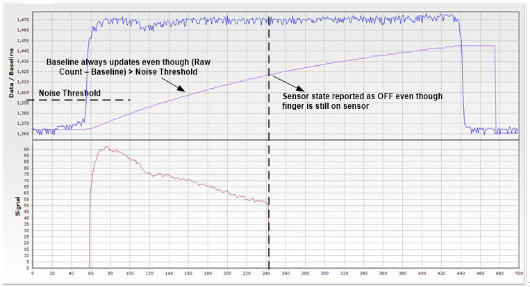
Because the baseline is always updated when sensor auto reset is enabled, this setting limits the maximum time duration for which the sensor will be reported as pressed. However, enabling this parameter prevents the sensors from permanently turning on if the raw count suddenly rises without anything touching the sensor. This sudden rise can be caused by a large power supply voltage fluctuation, a high-energy RF noise source, or a very quick temperature change.
Enable this option if you have a problem with sensors permanently turning on when the raw count suddenly rises without anything touching the sensor.
Multi-frequency scan
Enabling multi-frequency scan, the CAPSENSE™ component performs a sensor scan with three different sense clock frequencies and obtains corresponding difference count. The median of the sensor difference-count is selected for further processing. Use this feature for robust operation in the presence of external noise at a certain sensor scan frequency. This option is not available in SmartSense Full Autotune mode. See the code example
CE227719 CAPSENSE™ with multi-frequency scan
.
Button widget tuning
illustrates an overview of the CSD button tuning procedure.
Figure 120. CSD button widget tuning flowchart
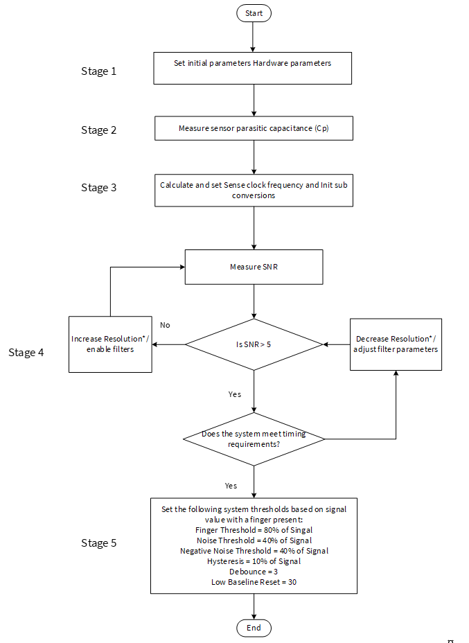
Attention: For fifth-generation CAPSENSE™, change number of sub-conversions (NSub) instead of resolution.
To review the hardware design, see the
Sensor construction
and
PCB layout guidelines
sections in the
Design considerations
chapter. Also, see the
Tuning debug FAQs
section for guidelines on advanced debug.
As explained in
Selecting between SmartSense and manual tuning
, Manual tuning requires effort to tune optimum CAPSENSE™ parameters, but allows strict control over characteristics of capacitive sensing system, such as response time and power consumption. The button is tuned for reliable touch detection to avoid false triggers in noisy environment.
The
CE230926 PSOC™ 4: CAPSENSE™ CSD button tuning
explains tuning of self-capacitance based button widgets in the Eclipse IDE for ModusToolbox™ using the CAPSENSE™
Tuner GUI
. For details on the Component and all related parameters, see the
Component datasheet
.
Slider widget tuning
A slider has many segments, each of which is connected to the CAPSENSE™ input pins of the PSOC™ device. Unlike the simple on/off operation of a button widget sensor, slider widget sensors work together to track the location of a finger or other conductive object. Because of this, the slider layout design should ensure that the
C
P
of all the segments in a slider remain as close as possible. Keeping similar
C
P
values between sensors will help minimize the tuning effort and ensure an even response across the entire slider. See
Slider design
for details on slider layout design guidelines to avoid nonlinearity in the centroid, ensure that the signal from all the slider segments is equal, as
Figure 121
shows, when a finger is placed at the center of the slider segment. If the signal of the slider segments is different, then the centroid will be nonlinear, as
Figure 122
shows.
Note: In PSOC™ Creator and in ModusToolbox™, a centroid of 0xFFFF and 0x0000 is reported respectively when a finger is not detected on the slider, or when none of the slider segments report a difference count value greater than the Finger Threshold parameter.
Figure 121. Response of centroid versus finger location when signals of all slider elements are equal
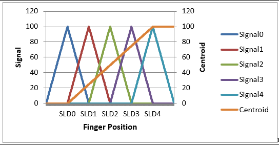
Note: Signal = Raw Count – Baseline
Figure 122. Response of centroid versus finger location when the signal of all slider elements are different
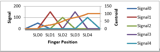
A linear response for the reported finger position (that is, the Centroid position) versus the actual finger position on a slider requires that the slider design is such that whenever a finger is placed anywhere between the middle of the segment SLDn and middle of segment SLDn-1, other than the exact middle of slider segments, exactly two sensors report a valid signal
10
. If a finger is placed at the exact middle of any slider segment, the adjacent sensors should report a difference count = noise threshold. These conditions are required since the centroid position calculation is based on the closest segment to the finger and two neighboring segments as shown in
Figure 123
.
Figure 123. Centroid algorithm used by CAPSENSE™ component in PSOC™
Where,
Resolution = API resolution set in the CAPSENSE™ Component Customizer
n = Number of sensor elements in the CAPSENSE™ Component Customizer
x = Index of element which gives maximum signal
s i
= Different counts (with subtracted noise threshold value) of the slider segment
shows an overview of the CSD slider tuning procedure.
Figure 124. CSD slider widget tuning flowchart
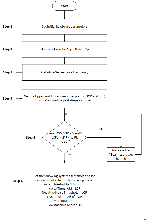
Attention: For fifth-generation CAPSENSE™, change number of sub-conversions (NSub) instead of resolution.
The upper crossover point (UCP) and lower crossover point (LCP) are obtained as shown in
Figure 125
. Refer to
CE229521 – PSOC™ 4 CAPSENSE™ CSD Slider tuning
which demonstrates how to manually tune a self-capacitance based Slider widget on PSOC™ Creator and
CE230493 – PSOC™ 4: CAPSENSE™ CSD Slider tuning
on Eclipse IDE for ModusToolbox™.
Figure 125. Difference count (delta) vs finger position
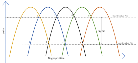
Touchpad widget tuning
Proximity widget tuning
CSX sensing method (third- and fourth-generation)
This chapter explains the basics of manual tuning using the CSX sensing method. It also explains the hardware parameters that influence a manual tuning procedure.
Basics
Conversion gain and CAPSENSE™ signal
In a mutual-capacitance sensing system, the
Rawcount
counter
is directly proportional to the mutual-capacitance between the Tx and Rx electrodes, as
Figure 126
shows.
Figure 126. Raw count relationship to sensor capacitance
Where,
G CSX
= Capacitance to digital conversion gain of CAPSENSE™ CSX
C M
= Mutual-capacitance between the Tx and Rx electrodes.
shows the relationship between raw count and mutual capacitance of the CSX sensor. The tunable parameters of the conversion gain in
Figure 127
are
F
TX
,
N
MOD
,
F
MOD
and IDAC.
The approximate value of this conversion gain is:
Figure 127. Capacitance to digital converter gain
Figure 128. MaxCount equation
Where,
V
TX
= Voltage at the Tx node of the sensor as shown in
Figure 129
The value of
V
TX
is always
V
DDIO
or
V
DDD
(if
V
DDIO
is not available) if the Tx clock frequency can completely charge and discharge the Tx electrode.
F
TX
is the Tx clock frequency,
I
DAC
is the current drawn for charging and discharging the
C
INT
capacitors, and
N
sub
is the number of sub-conversions.
Figure 129. Voltage at Tx node of the CSX sensor

Note: The raw count observed from the Component is given byFigure 130. See CAPSENSE™ CSX sensing method (third- and fourth- generation) for more details on Rawcountcomponent.
Figure 130. RawcountComponent
Figure 131. Raw count vs Sensor mutual-capacitance
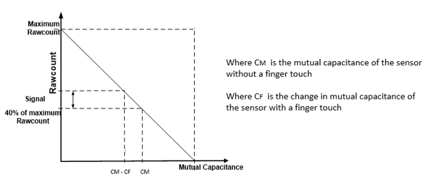
Selecting CAPSENSE™ hardware parameters
CAPSENSE™ hardware parameters govern the conversion gain and.
Table 16
lists the CAPSENSE™ hardware parameters that apply to the CSX sensing method.
Table 16
also shows the mapping of each parameter in the PSOC™Creator CAPSENSE™ component to the one in the ModusToolbox™ middleware. For simplicity of documentation, this design guide shows selecting the CAPSENSE™ parameter using the CAPSENSE™ configurator in PSOC™ Creator. The same procedure could be followed in configuring CAPSENSE™ in ModusToolbox™. However, in ModusToolbox™, you set the Tx clock and Modulator clock using divider values. On the other hand, in PSOC™ Creator, you specify the frequency value directly in the configurator. See
Component datasheet/middleware document
.
Sl # | CAPSENSE™ parameter in PSOC™ Creator | CAPSENSE™ parameter in ModusToolbox™ |
|---|---|---|
1 | Modulator clock frequency | Modulator clock divider |
2 | Tx clock source | Tx clock source |
3 | Tx clock frequency | Tx clock divider |
4 | IDAC | IDAC |
5 | Number of sub-conversions | Number of sub-conversions |
Tx clock parameters
There are two parameters that are related to the Tx clock: Sense clock source and Sense clock frequency.
Tx clock source
Select “Auto” to let the Component automatically choose the best Tx clock source between Direct and Spread spectrum clock (SSCx) for each widget. If not selecting Auto, select the clock source based on the following:
Direct – Clock signal with a fixed clock frequency. Use this option for most cases
Spread spectrum clock (SSCx) – If you chose this option, the Tx clock signal frequency is dynamically spread over a predetermined range. Use this option for reduced EMI interference and avoiding Flat-spots
However, when selecting SSCx clock, you need to select the Tx clock frequency, Modulator clock frequency, and number of sub conversion such that the conditions mentioned in
Component datasheet
/
ModusToolbox™ CAPSENSE™ configurator guide
for SSCx clock source selection are satisfied.
Tx clock frequency
The Tx clock frequency determines the duration of each sub-conversion as explained in the CAPSENSE™ CSX sensing method (third- and fourth- generation) Chapter. The Tx clock signal must completely charge and discharge the sensor parasitic capacitance; it can be verified by checking the signal in an oscilloscope, or it can be set using the Figure 132 . In addition, you should ensure that the auto-calibrated IDAC code lies in the mid-range (for example, 30-90) for the selected . If the auto-calibrated IDAC code lies out of the recommended range, tune such that it IDAC falls in the recommended range and satisfies Figure 132.
Figure 132. Condition for selecting Tx clock frequency
To minimize the scan time, as
Figure 133
shows, it is recommended to use the maximum Tx clock frequency available in the component drop-down list that satisfies the criteria.
Figure 133. Scan time of CSX sensor
Where,
N
Sub
=
Number of sub-conversions
.
Additionally, if you are using the SSCx clock source, ensure that you select the Tx clock frequency that meets the conditions mentioned in
Component datasheet/middleware document
/
ModusToolbox™ CAPSENSE™ configurator guide
in addition to these conditions.
The maximum value of
FTX
depends on the selected device. For the PSOC™ 4 S-Series, PSOC™ 4100S Plus, PSOC™ 4100PS, and PSOC™ 6 MCU family of devices, the maximum
FTX
is 3000 kHz and for other devices it is 300 kHz.
Modulator clock frequency
It is best to choose the highest allowed clock frequency for the given device because a higher modulator clock frequency leads to a higher sensitivity/signal, increased accuracy, and lower noise for a given
C
M
to digital count conversion as
Figure 107
and
Figure 108
indicate. Also, a higher value of
F
mod
/
F
tx
ensures lower width of
Flat-spots
in
C
M
to raw count conversion.
IDAC
It is recommended to enable IDAC auto-calibration. It is best to avoid very high and very low IDAC codes. The recommended IDAC code range is between 30-90. If the IDAC values are away from the recommended range, tune the Tx clock frequency to adjust the IDAC level. If the IDAC is failing to calibrate properly, it may be due to low
C
M
in the design. Refer to the section
I am observing a low CM for my CSX button
for mitigating impact of low
C
M
in the design.
Number of sub-conversions
The number of sub-conversions decides the sensitivity of the sensor and sensor scan time. From Figure 57 for a fixed modulator clock and Tx clock, increasing the number of sub-conversions ( NSub ) increases the signal and SNR. However, increasing the number of sub-conversions also increases the scan time of the sensor per Figure 134.
Figure 134. CSX scan time
Initially, set the value to a low number (for example, 20), and use the Tuner GUI to find the SNR of the sensor. If the SNR is not > 5:1 with the selected
N
Sub
, try to increase the
N
Sub
in steps such that the SNR requirement is met.
Selecting CAPSENSE™ software parameters
CAPSENSE™ software parameters for mutual-capacitance are the same as that for self-capacitance; therefore, these parameters could be selected as mentioned in the section Selecting CAPSENSE™ software parameters Selecting CAPSENSE™ software parameters.
Button widget tuning
illustrates an overview of the CSX button tuning procedure.
Figure 135. CSX button widget tuning example
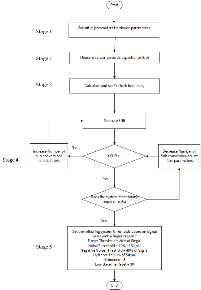
- To review the hardware design, see the
Sensor construction
and
PCB layout guidelines
sections in the
Design considerations
chapter. Also, see the
Tuning debug FAQs
section for guidelines on advanced debug
The
CE230660 PSOC™ 4: CAPSENSE™ CSX button tuning
explains tuning of mutual-capacitance based button widgets in the Eclipse IDE for ModusToolbox™ and
CE228931 – PSOC™ 4 CAPSENSE™ CSX button tuning
in PSOC™ Creator using the CAPSENSE™ tuner. For details on the Component and all related parameters, see the
Component datasheet
.
Touchpad widget tuning
CSD-RM sensing method (fifth-generation and fifth-generation low-power)
This chapter explains the basics of manual tuning using CSD-RM sensing method (Fifth-Generation and Fifth-Generation Low-Power). It also explains the hardware and software parameters that influence the CSD-RM sensing method and the procedure of manual tuning for button, slider, touchpad and proximity widgets.
Basics
Conversion gain and CAPSENSE™ signal
Conversion gain will influence how much signal the system sees for a finger touch on the sensor. If there is more gain, the signal is higher, and a higher signal means a higher achievable Signal-to-noise ratio (SNR).
Note: An increased gain may result in an increase in both signal and noise. However, if required, you can use firmware filters to decrease noise. For details on available firmware filters, seeTable 11.
Conversion gain in single CDAC
In the single CDAC mode, the raw count is directly proportional to the sensor capacitance.
Figure 136. Raw count relationship to sensor capacitance
Where,
C S
= Sensor capacitance
C S
=
C
P
if there is no finger present on sensor
C S
= (
C
P
+
C
F
) when there is a finger present on the sensor
G CSD
= Capacitance to digital conversion gain of CAPSENSE™ CSD. The approximate value of this conversion gain according to
Figure 66
and
Figure 136
is shown using
Figure 137
.
Figure 137. Capacitance to digital converter gain
Where,
The equation for raw count in the single CDAC mode, according to
Figure 137
and
Figure 136
is shown in
Figure 138
.
Figure 138. Single CDAC mode raw counts
Where,
N Sub
= Number of sub-conversions
SnsClk Div
= sense clock divider
C S
= Sensor capacitance
C ref
= Reference capacitance
RefCDACCode = Reference CDAC value
The tunable parameters of the conversion gain are
C
ref
,
SnsClk
Div
, and
N
Sub
.
Figure 139
shows a plot of raw count versus sensor capacitance.
Figure 139. Raw count versus sensor capacitance
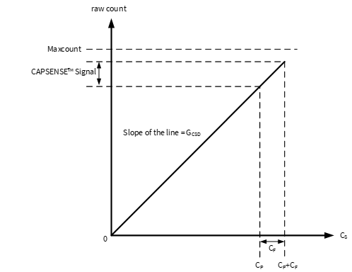
The change in raw counts when a finger is placed on the sensor is called CAPSENSE™ signal.
Figure 140
shows how the value of the signal changes with respect to the conversion gain.
Figure 140. Signal values for different conversion gains
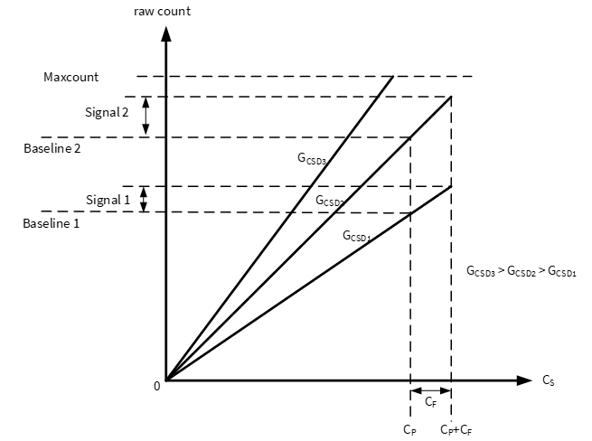
shows three plots corresponding to three conversion gain values
G
CSD3
,
G
CSD2
, and
G
CSD1
. An increase in the conversion gain results in higher signal value. However, this increase in the conversion gain also moves the raw count corresponding to
C
P
(that is, Baseline) towards the maximum value of raw count (Maxcount). For very high gain values, the raw count saturates as the plot of
G
CSD3
shows. Therefore, tune the conversion gain to get a good signal value while avoiding saturation of raw count. Tune the CSD-RM parameters such that when there is no finger on the sensor, that is when
C
S
=
C
P
, the raw count = 85% of Maxcount as
Figure 141
shows. This ensures maximum gain, with enough margin for the raw count to grow because of environmental changes, and not saturate on finger touches.
Figure 141. Recommended tuning
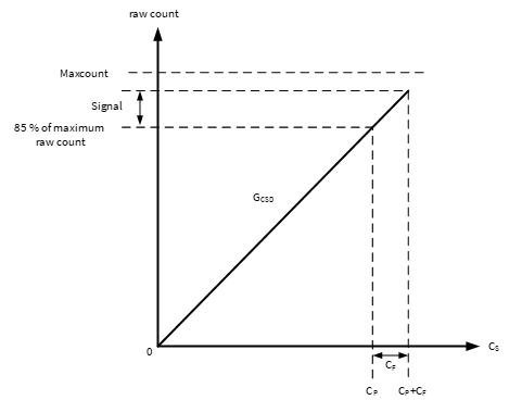
Conversion gain in dual CDAC mode
The equation for raw count in the dual CDAC mode, according to
Figure 67
and
Figure 136
is shown in
Figure 142.
Figure 142. Dual CDAC mode raw counts
Where,
Maxcount =
N
Sub
*
SnsClk
Div
SnsClk Div
= Sense clock divider
N Sub
= Number of sub-conversions
C ref
= Reference capacitance
C comp
= Compensation capacitance
CompCLK Div
= CDAC compensation divider
C S
= Sensor capacitance
C ref
= RefCDACCode *
C
lsb
C comp
=CompCDACCode *
C
lsb
RefCDACCode = Reference CDAC value
CompCDACCode = Compensation CDAC value
C lsb
= 8.86fF
G CSD
is given by
Figure 137
.
In both single CDAC and dual CDAC mode, tune the CSD-RM parameters, so that when there is no finger on the sensor, that is when
C
S
=
C
P
, the raw count = 85% of Maxcount, as
Figure 143
shows, to ensure high conversion gain, to avoid
Flat-spots
, and to avoid raw count saturation due to environmental changes.
Figure 143. Recommended tuning in dual CDAC mode
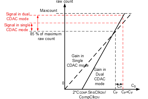
As Figure 143 shows, the 85% requirement restricts to a fixed gain in single-CDAC mode, while in dual-CDAC mode, gain can be increased by moving the CS axis intercept to the right (by increasing CompClk DIV ) and correspondingly decreasing the modulator CDAC switching ( SnsClk DIV ) to still achieve raw count = 85% of Maxcount for CS= CP . Using dual CDAC mode this way brings the following changes to the Raw Count versus CP graph:
Use of compensation CDAC introduces a non-zero intercept on the CS axis as shown in Figure 144
Figure 144. CS axis intercept with regards to C comp
The value of C ref in the dual CDAC mode is half compared to the value of Cref in the single CDAC mode (all other parameters remaining the same), so the gain GCSD in the dual CDAC mode is double the gain in the single CDAC mode according to Figure 96 . Thus, the signal in the dual CDAC mode is double the signal in the single CDAC mode for a given number of sub-conversions ( N sub ).
While manually tuning a sensor, refer
Figure 96
,
Figure 101
and the following points:
Higher gain leads to increased sensitivity and better overall system performance. However, do not set the gain such that raw counts saturate, as the plot of gain G CSD3 shows in Figure 99 . It is recommended to set the gain in such a way that the raw count corresponding to C P is 85 percent of the maximum raw count for both the single CDAC and dual CDAC mode
The sense clock frequency ( FSW ) should be set carefully; higher the frequency, higher the C S sampling rate which allows for more FSW periods and better noise averaging, but the frequency needs to be low enough to fully charge and discharge the sensor as Figure 108 indicates
Enabling the compensation CDAC (baseline compensation) plays a huge role In increasing the gain; it will double the gain if set as recommended in Conversion gain in dual CDAC mode . Always enable Compensation CDAC, make sure the calibrated Cref is in valid range when enabling Compensation CDAC
Lower the reference CDAC, higher the gain. Adjust your CDAC to achieve the highest gain, but make sure that the raw counts corresponding to CP have enough margin for environmental changes such as temperature shifts, as indicated in Figure 100 and Figure 102
Increasing the number of sub-conversions used for scanning increases gain. An increase in number of sub-conversions also increases the scan time according to Figure 49 . A balance of scan time and gain need to be achieved using number of sub-conversions ( Nsub )
Flat-spots
Ideally, raw counts should have a linear relationship with sensor capacitance as
Figure 98
and
Figure 102
show. However, in practice, RM converter has non-sensitivity zones, also called flat-spots or dead-zones – for a range of sensor capacitance values, the RM converter may produce the same raw count value as
Figure 146
shows. This range is known as a dead-zone or a flat-spot.
shows the flat-spots relation to different CAPSENSE™ hardware parameters.
Figure 145. Flat-spots width
Where,
C S
= Sensor capacitance
C MOD
= Modulator capacitor
F SW
= Frequency of the sense clock
F MOD
= Modulator clock frequency
Bal% = Rawcount calibration percentage
Figure 146. Flat-spots in raw counts versus sensor capacitance when direct clock is used
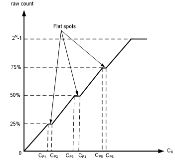
Flat-spots reduction techniques
Set rawcount calibration to 85%
As per
Figure 145
, flat-spots width is inversely proportional to calibration level. Setting calibration to 85% decrease the width of flat-spots significantly.
Enable dithering
An additional Dither CDAC is available in Fifth-Generation CAPSENSE™ architecture, which adds white noise that moves the conversion point around the flat-spots region.
Enable PRS clock
These flat-spots are prominent when direct clock is used as
Sense clock
source. Flat-spots are reduced if PRS is used as the sense clock source (see also section
Using SmartSense to determine hardware parameters
). PRS clock can results in a slight reduction of signal or sensitivity at higher rawcount calibration. Recommended to set the rawcount calibration to 65% when PRS is used as clock source.
Use larger CMOD
The flat-spots width is inversely proportional to the
C
MOD
used. Fifth-Generation architecture supports
C
MOD
upto 10 nF and typical value is 2.2 nF. And increasing
C
MOD
have the adverse effect of increasing the noise, initialization time and minimum signal required to detect.
Increase sense clock divider
Increasing sense clock divider decreases flat-spots width but increases the scan time. If the flat-spot is detected, increase the Sense clock divider such that the scan time requirement is met.
lists different the flat-spots reduction techniques in recommended priority and other considerations.
S. No | Flat-spots reduction techniques | Recommendation | Additional benefits | Disadvantage |
|---|---|---|---|---|
1 | Set rawcount calibration to 85%. | High | Improves sensitivity | - |
2 | Enable dithering | High | - | - |
3 | Enable PRS clock | Low | Improves EMI/EMC radiation | Needs to set rawcount calibration to 65%. Decreases sensitivity. |
4 | Increase C MOD | Low | - | Increases noise |
5 | Increase sense clock divider | Low | - | Increases scan time and power consumption |
Selecting CAPSENSE™ hardware parameters
CAPSENSE™ hardware parameters govern the conversion gain and CAPSENSE™ signal.
Table 18
lists the CAPSENSE™ hardware parameters that apply to CSD-RM sensing method. The following subsections provide guidance on how to adjust these parameters to achieve optimal performance for CAPSENSE™ CSD-RM system.
S. No | CAPSENSE™ parameter in ModusToolBox™ |
|---|---|
1 | Scan mode |
2 | Scan connection method |
3 | Number of Init sub-conversions |
4 | Sense clock divider |
5 | Sense clock source |
6 | Modulator clock divider |
7 | Reference CDAC value |
8 | CDAC compensation divider |
9 | Compensation CDAC value |
10 | Fine CDAC value |
11 | Number of sub-conversions |
12 | Enable CDAC dither |
show selecting the CAPSENSE™ parameters in Eclipse IDE for ModusToolbox™. For more details on configuring CAPSENSE™, see the
Component datasheet/middleware document
.
Manually tuning hardware parameters
Scan mode
Scan mode can be set as CS-DMA or Interrupt Driven mode. For autonomous scanning select DMA mode and for legacy interrupt based scanning select Interrupt Driven mode.
In Fifth-Generation Low-Power CAPSENSE™, autonomous scanning is supported inherently and does not need CPU intervention, and does not require CTRLMUX and DMA.
Sensor connection method
Autonomous scanning is only available in CTRLMUX method, but the numbers of supported pins are limited in this method (see the
Device datasheet
for supported pins). Additionally provides better immunity to on-chip IO noise. Choose AMUXBUS method to support more number of pins in Interrupt Driven mode.
In Fifth-Generation Low-Power CAPSENSE™, all CAPSENSE™ pins support autonomous scanning mode, via the AMUXBUS, compared to the limited number of pins which were supported by the CTRLMUX in the Fifth-Generation CAPSENSE™ technology.
Modulator clock frequency
The modulator clock governs the conversion time for capacitance-to-digital conversion, also called the “sensor scan time” (see
Figure 49
).
A lower modulator clock frequency implies the following:
Longer conversion time
Lower peak-to-peak noise on raw count because of longer integration time of the ratiometric converter
Wider Flat-spots
Select the highest frequency for the shortest conversion time and narrower flat-spots for most cases. Use slower modulator clock to reduce peak-to-peak noise in raw counts if required.
Based on the required Modulator clock frequency (
F
MOD
), calculate the modulator clock divider using
Figure 147
.
Figure 147. Modulator clock divider
Where,
F Clock
= Clock frequency connected to CAPSENSE™ block
Initialization sub-conversions
As part of initialization,
C
MOD1
and
C
MOD2
need to be charged to the required voltage (VDDA/2). There are three phases in initialization –
C
MOD
initialization,
C
MOD
short and initialization sub-conversions. During
C
MOD
initialization phase,
C
MOD1
is pulled to GND and
C
MOD2
is pulled to VDDA. During
C
MOD
short phase both capacitors are tied together so the charge is shared to produce a voltage close to VDDA/2 on both. After these two phases the scanning is started, but rawcount is discarded for the configured number of init sub-conversions.
The number of init sub-conversions should be selected based on
Figure 148
.
or
Figure 148. Number of init sub-conversions
Where,
C MOD
= Modulator capacitor
V OS = Comparator offset voltage (3 mV)
Note: Use Vos=4 mV for Automotive grade (E-grade) devices
C S
= Sensor capacitance
Base% = Baseline compensation percentage
Bal% = Rawcount calibration percentage
SnsClk Div
= sense clock divider
C ref
= Reference capacitance
C ref
= RefCDACCode * C lsb
RefCDACCode = Reference CDAC value
C lsb = 8.86 fF
Note: In the case of CSD, it is recommended not to check the "Enable coarse initialization bypass" parameter by default. If power requirements are not met, try enabling it but check supply rejection.
Sense clock parameters
There are two parameters that are related to Sense clock: Sense clock source and Sense clock divider.
Sense clock source
Select “Auto” to let the Component automatically choose the best Sense clock source from Direct, PRSx, and SSCx for each widget. If not selecting Auto, select the clock source based on the following:
Use SSCx (spread spectrum clock) modes for reducing EMI/EMC noise at a particular frequency. This feature is available in PSOC™ 4S-Series, PSOC™ 4100S Plus, PSOC™ 4100PS, PSOC™ 4100S Max, PSOC™ 4000T, PSOC™ 4100T Plus and PSOC™ 6 family of devices. In this case, the frequency of the sense clock is spread over a predetermined range
Use Direct clock for absolute capacitance measurement
Use PRSx (pseudo random sequence) modes to remove flat-spots and improve EMI/EMC radiation. In 5 th Generation CAPSENSE™, PRS clock results in a slight reduction in signal/sensitivity at higher rawcount calibration percent, hence 65% rawcount calibration is recommended when PRS clock is used
When selecting SSCx, you need to select the Sense clock frequency, Modulator clock frequency, and number of sub-conversion such that the conditions mentioned in
ModusToolbox™ CAPSENSE™ configurator guide
for SSCx clock source selection are satisfied.
PRS/SSC can be used to reduce the emissions, but it will increase power consumption as it needs high Nsubs. It is recommended to set Nsubs as 1024(or multiples of 1024) to obtain the maximum spread. If Nsubs are lesser than 1024 or non-multiples of 1024, the performance will be non-optimal.
Sense clock divider
The sense clock divider should be selected so that the sensor will charge and discharge completely in each sense clock period.
This is verified by observing the charging and discharging waveforms of the sensor using an oscilloscope and an active probe. The sensors should be probed close to the electrode and not at the sense pins or the series resistor.
Note: Fifth-Generation CSD-RM charging and discharging happen twice in a single clock period.
Refer to
Figure 149
and
Figure 150
for waveforms observed on the sensor/shield.
Figure 149
shows proper charging when the sense clock frequency is correctly tuned. The pulse width is at least 5Tau, that is, the voltage is reaching at least 99.3% of the required voltage at the end of each phase.
Figure 150
shows incomplete settling (charging/discharging). If the charging is incomplete, increase the sense clock divider.
Figure 149. Proper charge cycle of a sensor
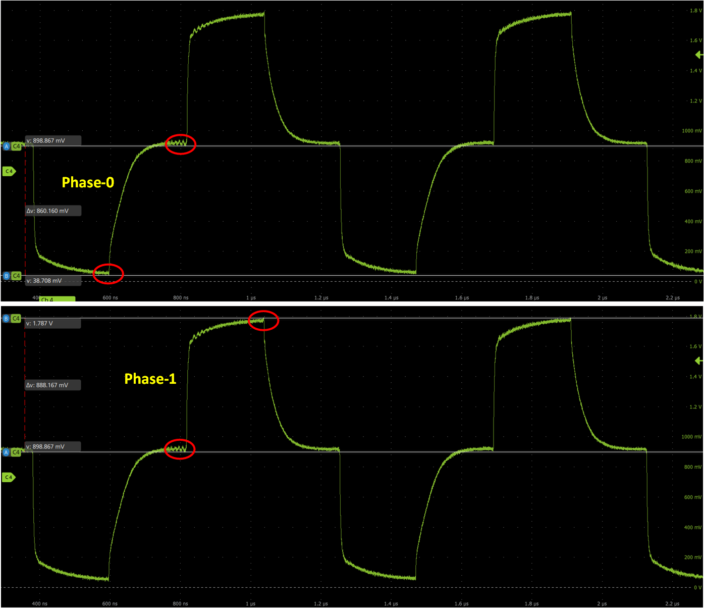
Figure 150. Improper charge cycle of a sensor
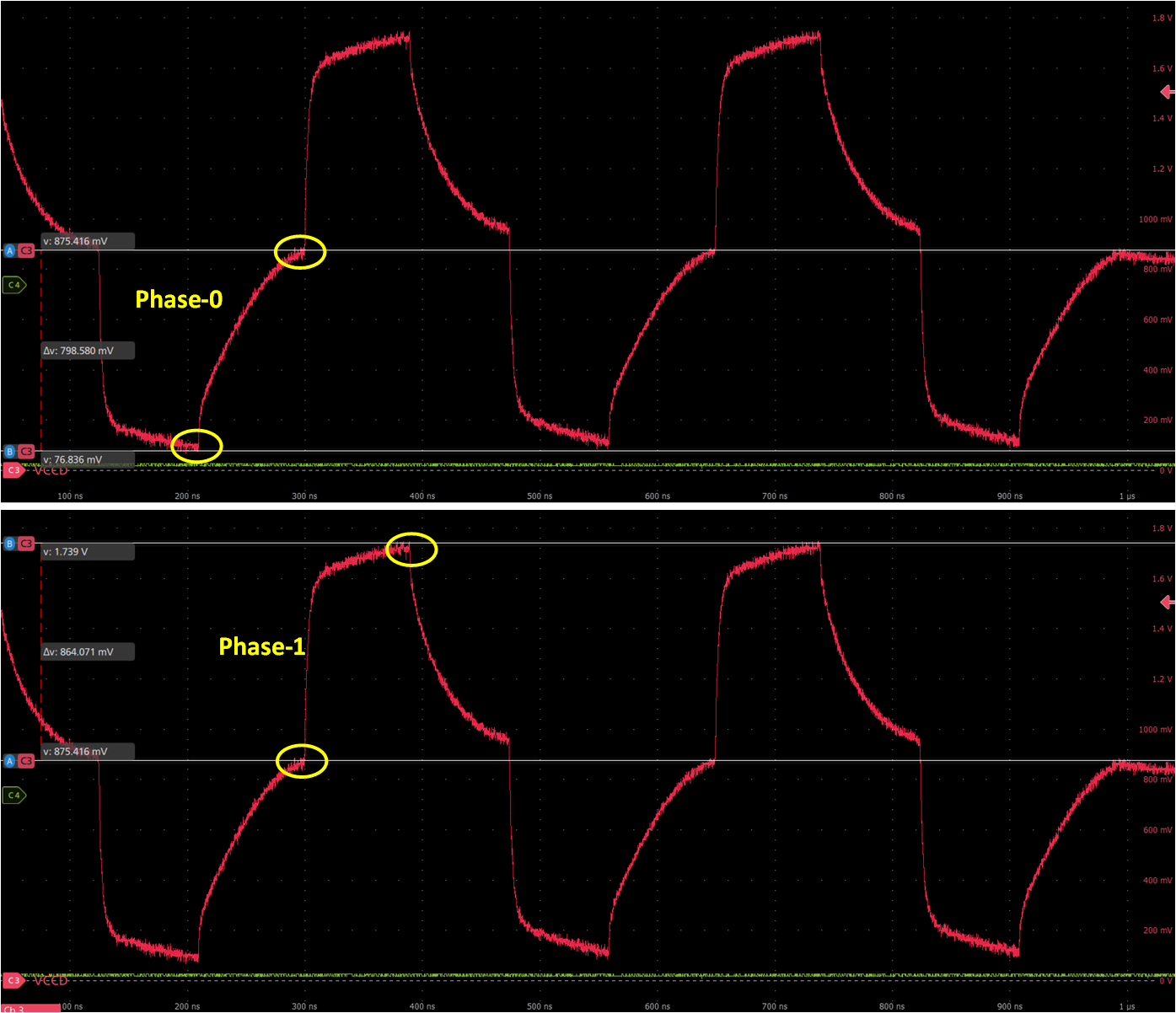
Note: The sense clock divider should be divisible by 4. This ensures that all four scan phases have equal durations.
Repeat this process for all the sensors and the shield. Each sensor may require a different sense clock divider value to charge/discharge completely. But all the sensors that are in the same scan slot need to have the same sense clock source, sense clock divider, and number of sub-conversions. Therefore, take the largest sense clock divider in a given scan slot and apply it to all the other sensors that share that slot. Take this into consideration that a higher sense clock divider increases current consumption as there are longer charging and discharging cycles. Generally, the
C
P
of the shield electrode will be higher compared to the sensor
C
P
.
For good liquid tolerance, the shield signal should satisfy the condition mentioned in the
Tuning shield electrode
chapter. If it is not satisfied, reduce the sense clock frequency further to satisfy the condition.
Figure 151. Sense clock divider
shows that it is best to use the maximum clock frequency to achieve higher gain; however, you should ensure that the sensor capacitor fully charges and discharges as shown in
Figure 63
.
Number of sub-conversions
The number of sub-conversions decides the sensitivity of the sensor and sensor scan time. From
Figure 67
for a fixed modulator clock and Sense clock, increasing the number of sub-conversions (
N
Sub
) increases the signal and SNR. However, increasing the number of sub-conversions also increases the scan time of the sensor per
Figure 152
.
Figure 152. CSD-RM scan time
Initially, set the value to a low number, and use the Tuner GUI to find the SNR of the sensor. If the SNR is not > 5:1 with the selected, try to increase the in steps such that the SNR requirement is met.
Note: Number of sub-conversions should be greater than or equal to 8 to allow the CDAC dithering to function optimally. When using PRS/SSC it should be multiples of 1024 for optimal performance.
Capacitive DACs
Fifth-Generation CAPSENSE™ supports three CDACs: Reference CDAC ( Cref ), Fine CDAC (Cfine), and Compensation CDAC ( C comp) that balance C MOD ’s, as Figure 59 shows. These govern the Conversion gain and CAPSENSE™ signal for capacitance-to-digital conversion. CAPSENSE™ allows the following configurations of the CDACs:
Enabling or disabling of Compensation CDACs
Enabling or disabling of Auto-calibration for the CDACs
Compensation CDAC divider and DAC codes for Reference and Compensation CDACs can be set manually if auto-calibration is disabled
is applicable only for fifth-generation low-power which showcases different numbers of valid CDAC combinations that can be set in the CAPSENSE™ configurator.
Sr. no. | C ref | C fine | C comp |
|---|---|---|---|
1 | Auto | Auto | Auto |
2 | Auto | Auto | Disabled |
3 | Auto | Disabled | Auto |
4 | Auto | Disabled | Disabled |
5 | Value | Value | Auto |
6 | Value | Value | Value |
7 | Value | Value | Disabled |
8 | Value | Disabled | Auto |
9 | Value | Disabled | Value |
10 | Value | Disabled | Disabled |
11 | Disabled | Auto | Auto |
12 | Disabled | Auto | Disabled |
13 | Disabled | Value | Auto |
14 | Disabled | Value | Value |
15 | Disabled | Value | Disabled |
Note: It is recommended to always enable auto-calibration for the CDACs. This will ensure optimal tuning.
C
ref
boost parameter can be used to adjust the sensitivity of reference CAPDAC, which can be used only with combinations 1 and 3, where Compensation CDAC (C
comp
) and reference CAPDAC are set to "Auto".
Capacitive DACs scaling
CDACs have some inherent tolerance which could lead to variation in the Signal observed across units. To aid in minimizing this variation, MSCLP devices have CDAC trim codes in SFLASH (read-only). This code is used to scale the Reference CDAC and Fine CDAC parameters, which compensates for variations in the CDAC and brings down the overall signal variation across units
Note: This feature is currently applicable to the PSOC™ 4100T Plus device only.
The effective parasitic capacitance (Cp) of the sensor mainly depends on 𝑪𝒔𝒆𝒏𝒔𝒐𝒓 & 𝑪𝒑𝒊𝒏,
Csensor: capacitance of the sensor electrode & traces excluding the device pin
Cpin: Capacitance of the device pin
Note: The measured Cp in capacitance for PSOC™ 4100T Plus is ~2.77 pF.
When the effective Cp measured out of BIST is very small (<4pF), the Cpin capacitance becomes a significant contributor to the Cp and has an impact on signal variation.
To mitigate this issue, the middleware reads and utilizes the trim codes stored in the device SFLASH memory to scale the CDAC values; specifically Reference CDAC (Cref) and Fine CDAC (Cfine).
CDAC scaling is appliable only in the following scenarios,
Sensor Cp is less than 4pF
Widget type is CSD (regular and low power)
Reference CDAC and Fine CADC are set to 'Manual' mode
Note: If sensor Cp is more than 4pF configure CDAC tuning mode as 'Auto'.
Tuning recommendation
For a step-by-step guide on the tuning procedure, please refer to Stage 3 of the code example Readme for CE238886 – PSOC™ 4: MSCLP low-power self-capacitance button.
Reference CDAC (Cref)
The reference CDAC is used to compensate for the charge transferred by the sensor self-capacitance (
C
S
) from the
C
MOD
. The number of times it is switched depends on the self-capacitance of the sensor. In the case of a finger placed over the sensor, additional reference CDAC switching is required to compensate.
C
ref
is calculated using the following equation:
Where,
RefCDACCode = Reference CDAC value
C lsb
= 8.86 fF
C ref
should satisfy the below criteria:
If the auto-calibrated RefCDACCode is less than 6, then enable fine CDAC.
The following options can be used to increase the RefCDACCode,
Decrease the sense clock divider. Note that the pulse width of the sense clock should be long enough to allow the sensor capacitance to charge and discharge completely. This decreased sense clock can be accommodated by decreasing series resistance or decreasing shield Cp
Disable compensation
Fine Reference CDAC (Cfine)
The fifth-generation low-power CAPSENSE™ consists of a Fine CDAC, which is a programmable CDAC used to achieve a finer resolution for the Reference CDAC. Hence, enabling Cfine along with Cref increases the accuracy. It is recommended to always enable auto-calibration for Fine CDAC to ensure optimal performance.
C
fine
= Fine Reference CDAC = FineCDACCode * C
lsb
FineCDACCode = Fine CDAC value
C
lsb
= 2.2 nF
Compensation CDAC (Ccomp)
Enabling the compensation CDAC is called “dual CDAC” mode, and results in increased signal as explained in Conversion gain and CAPSENSE™ signal . Enable the compensation CDAC for most cases.
The compensation capacitor is used to compensate excess self-capacitance from the sensor to increase the sensitivity. The number of times it is switched depends on the amount of charge the user application is trying to compensate (remove) from the sensor self-capacitance.
Compensation CDAC divider
The number of times the compensation capacitor is switched in a single sense clock is denoted by
K
comp
. Select CDAC compensation divider based on
Figure 153
such that below criteria is satisfied.
CDAC compensation divider >= 4
Kcomp should be a whole number
Figure 153. CDAC compensation divider
Auto-calibration
The auto-calibration feature enables the firmware to automatically calibrate the CDAC to achieve the required calibration target of 85%. It is recommended to enable auto-calibration for most cases. Enabling this feature will result in the following:
Default calibration is set to 85% of maximum raw count even with part-to-part C P variation
Note: If the raw counts are saturating at 85%, the calibration percentage can be reduced further to avoid saturation.
Decrease the effect of Flat-spots
If your design environment includes large temperature variation, you may find that the 85% CDAC calibration level is too high, and that the raw counts saturate easily over large changes in temperature, leading to lower SNR. In this case, adjust the calibration level lower by using
Cy_CapSense_CalibrateAllSlots()
in your firmware.
For proper functioning of CAPSENSE™ under diverse environmental conditions, it is recommended to avoid very low or high CDAC codes. For an 8-bit CDAC, it is recommended to use CDAC codes between 6-200 from the possible 0 to 255 range. You can use CAPSENSE™ tuner to confirm that the auto-calibrated CDAC values fall in this recommended range. If the CDAC values are out of the recommended range, based on
Figure 136
,
Figure 137
, and
Figure 142
, you may change the Calibration level or
F
mod
or
F
SW
to get the CDAC code in proper range.
Selecting CDAC codes
This is not the recommended approach. However, this approach could be used only if you want to disable auto-calibration for any reason. To get the CDAC code, you may first configure CAPSENSE™ Component with auto-calibration enabled and all other hardware parameters the same as required for final tuning and read back the calibrated CDAC values using
Tuner GUI
. Then, re-configure the CAPSENSE™ Component to disable auto-calibration and use the obtained CDAC codes as fixed DAC codes read-back from the
Tuner GUI
.
CDAC dither
As the input capacitance is swept, the raw count should increase linearly with capacitance. There are regions where the raw count does not change linearly with input capacitance, and these are called flat-spots. See section
Flat-spots
for more details. Dithering helps to reduce flat-spots. This is done using a dither CDAC. The dither CDAC adds white noise that moves the conversion point around the flat region.
It is recommended to always enable CDAC dither scale in auto-calibrated mode to ensure optimal performance. In case it is required to set the CDAC dither scale manually, see the following table for general recommended values.
Parasitic Capacitance (Cp) | Scale |
|---|---|
2 pF <= Cp < 3pF | 3 |
3 pF <= C p < 5 pF | 2 |
5 pF <= C p < 10 pF | 1 |
C p >= 10 pF | 0 |
For details on setting dither related parameters, refer to the Readme of code example
PSOC™ 4: MSCLP CAPSENSE™ low power (section '
Stage 2: Measure sensor capacitance to set CDAC Dither parameter
')
Tuning shield electrode
The shield related parameters need to be additionally configured or tuned differently when you enable the Shield electrode in the CSD-RM sensing method for liquid tolerance or reducing the
C
p
of the sensor.
Shield electrode tuning theory
Ideally, the shield waveform should be exactly the same as that of the sensor as explained in CAPSENSE™ CSDRM shielding . However, in practical applications, the shield waveform may have a higher settling time. Observe the sensor and shield waveform in the oscilloscope; an example waveform is shown in Figure 154 and Figure 155 . The shield waveform should settle to the sensor voltage within 90% of ON time of the sense clock waveform and the overshoot error of the shield signal with respect to VREF should be less than 10%.
If these conditions are not satisfied, you will observe a change in raw count of the sensors when touching the shield hatch; in addition, if inactive sensors are connected to shield as mentioned in
Inactive sensor connection
, touching one sensor can cause change in raw count on other sensors, which indicates that there is cross talk if the shield electrode is not tuned properly.
Note: The sense clock divider should bedivisible by 4. This ensures that all four scan phases have equal durations.
Keep in mind that the higher sense clock divider increases current consumption as there is longer charging and discharging cycles. Generally, the
C
P
of the shield electrode will be higher compared to the sensor
C
P
. For good liquid tolerance, approximate maximum shield frequency (
F
Shield
) ensures correct charging and discharging of the shield waveform. If it is not satisfied, reduce the sense clock frequency further to satisfy the condition.
In SmartSense, the sense clock frequency is automatically set. Check if these conditions are satisfied. If not satisfied, switch to
Manual tuning
and set the sense clock frequency manually so that these conditions are satisfied.
Figure 154. Properly tuned shield waveform (active shielding)
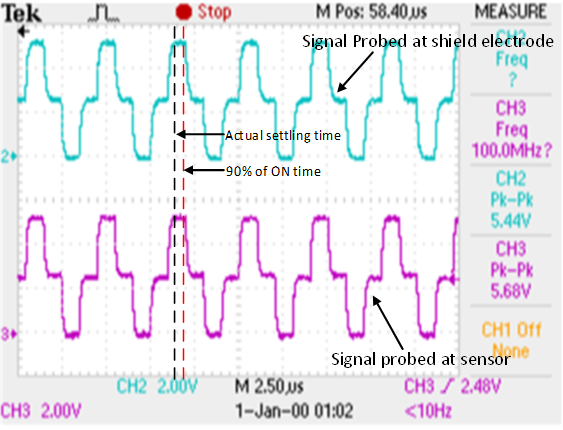
Figure 155. Properly tuned shield waveform (passive shielding)
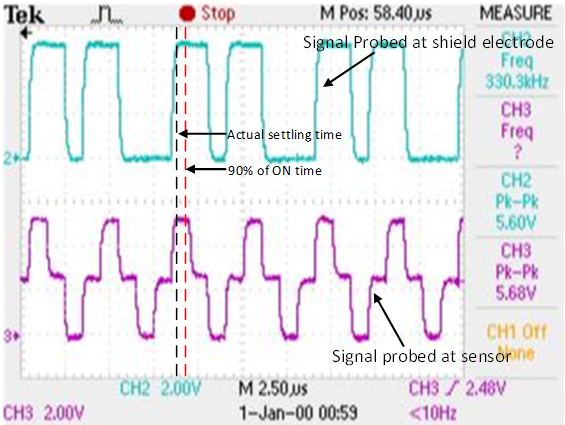
Tuning shield-related parameters
Inactive sensor connection
When the shield electrode is enabled for liquid-tolerant designs, or if you want to use shield to reduce the sensor parasitic capacitance, this option should be specified as “Shield”; otherwise, select “Ground”.
However, there is a risk of higher radiated emission due to inactive sensors getting connected to Shield. In such situations, use the CAPSENSE™ API to manually control inactive sensor connections. Instead of connecting all unused sensors to the shield, connect only the opposing inactive sensors or inactive sensors closer to the sensor being scanned to shield for reducing the radiated emission.
Number of shield electrodes (total shield count)
This parameter specifies the number of shield electrodes required in the design. Most designs work with one dedicated shield electrode; however, some designs require multiple dedicated shield electrodes for ease of PCB layout routing or to minimize the PCB real estate used for the shield layer. See
Layout guidelines for shield electrode
Layout guidelines for shield.
Shield mode
The Fifth-Generation CAPSENSE™ architecture supports two shield modes – active and passive shielding. See CAPSENSE™ CSDRM shielding section to decide which mode is best suited for your application.
Selecting CAPSENSE™ software parameters
CAPSENSE™ software parameters in Fifth-Generation are the same as that for Fourth-Generation; therefore, these parameters could be selected as mentioned in Selecting CAPSENSE™ software parameters section.
Configuring autonomous scan
Autonomous scanning improves CPU offloading by removing the requirement of CPU intervention in between sensor scans.
Figure 156
shows the waveform of scanning all slots, which shows the CAPSENSE™ CPU bandwidth requirement for autonomous scanning and interrupt driven scanning. In autonomous scan once the CPU initiates a command to scan all slots, there is no CPU interrupt raised by CAPSENSE™ until all the slots are scanned. But in interrupt driven scan, after each slot scan, a CPU interrupt is raised to configure the next slot sensors.
Figure 156. Autonomous Scanning versus Interrupt Driven Scanning
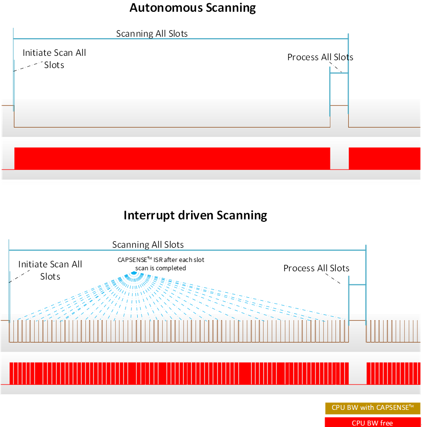
In fifth-generation CAPSENSE™, autonomous scanning is only available when Scan mode is set as Chained Scanning – DMA (CS-DMA) in the CAPSENSE™ configurator as shown in
Figure 157
. And sensor connection method is only available as CTRLMUX. This limits the number of available CAPSENSE™ sensors. In Interrupt driven mode, sensor connection can be configured as either AMUXBUS or CTRLMUX. Through AMUXBUS any GPIO pin can be configured as a CAPSENSE™ sensor,but CPU interrupts need to be serviced to read the scan result and configure the next sensor.
Figure 157. CAPSENSE™ configurator settings for scan mode
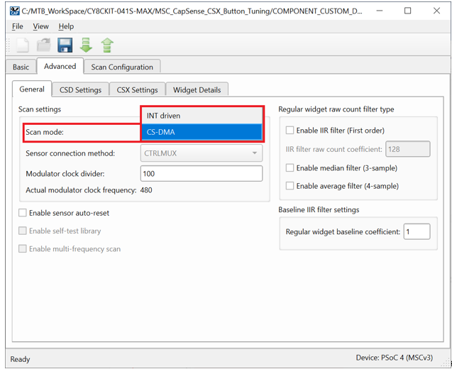
In fifth-generation low-power CAPSENSE™ regular widgets are scanned autonomously by default. CPU can remain in deep sleep mode while the scanning happens. An interrupt can wake the CPU to process the data, after all the slots are scanned Low power widgets are scanned using the low-power always-on-sense (LP-AoS) mode as explained in
LP-AoS mode
.
Autonomous scanning
Autonomous scanning mode in Fifth-Generation CAPSENSE™ technology avoids the CPU intervention for scanning every next sensor. This significantly reduces the CPU bandwidth required for scanning widgets withlarge number of sensors. Based on the CAPSENSE™ generation there are the following methods of autonomous scanning -
Chained scanning – DMA mode
and
LP-AoS mode
.
Chained scanning – DMA mode
In the chained scanning - DMA mode, DMA handles the configuration of each sensor, thereby avoiding the requirement of CPU intervention after each sensor scan completion. Each channel of MSC block requires four channels of DMA to be configured in the device configurator as shown in
Figure 158
.
Figure 158. DMA configuration for MSC channels
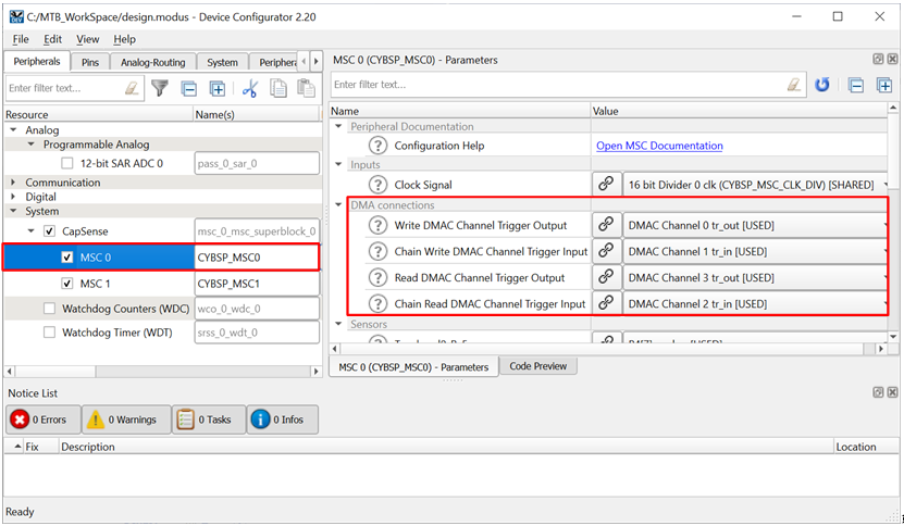
illustrates the flow of CS-DMA based scanning mode.
Write DMA channel
Write DMA is configured to transfer scan configuration of a sensor to MSC block. Source address to the corresponding sensor’s scan configuration is received from Chain Write DMA channel
Chain Write DMA channel
When the MSC block completes scanning of current sensor, it will trigger the DMA to transfer the source address of next sensor’s or first sensor’s (if it is a new scan) scan configuration to the Write DMA channel
Read DMA channel
Read DMA channel transfer the scan result (rawcount) to destination location of corresponding sensor
Chain Read DMA channel
Once the current sensor scan is completed by MSC block, Chain Read DMA is triggered to transfer the destination location (address) of current sensor scan result (rawcount) to the Read DMA channel
Figure 159. CS-DMA scanning flow
LP-AoS mode
The fifth-generation CAPSENSE™ (MSCLP) performs autonomous sensing using the LP-AoS hardware mode. Using this mode, multiple sensors (a frame) can be scanned without the intervention of the CPU. To enable this, the MSCLP block has an internal 1-KB SRAM. The middleware writes the configuration of multiple sensors to be scanned to the internal SRAM. Then, the MSCLP autonomously reads each sensor configuration, initiates scanning, and saves the result to the SRAM for the middleware to read and process after full-frame scanning is completed.
The device can be kept in any device power modes such as active, sleep, or deep sleep while MSCLP is scanning multiple sensors. MSCLP has all the system resources such as high-frequency clock and reference generator internal to the MSCLP hardware to enable scanning in device low-power state (i.e., deep sleep).
Wake-on-Touch (WoT)
LP-AoS has the additional capability of scanning the same frame periodically and processing the result to detect touch. Therefore, the CPU is not required to process or initiate scanning; this allows the PSOC™ device to be kept in deep sleep for a longer time and to have the sensor touch detection as a wakeup interrupt. This is known as Wake-on-Touch. With this approach, the application can get the lowest power consumption with touch-sensing capability. Note that WoT is only supported for Low-Power Widgets. See section
Low-power widget tuning
for details on Low-Power Widgets.
Figure 160. LP-AoS Mode

Multi-channel scanning
Multi-channel design uses both the instances of CAPSENSE™ MSC0 and MSC1, leading to simultaneous operation and reduction in scan time. Multi-channel scanning is in lock step thereby avoiding any cross-channel noise coupling. Scan synchronization is required to have the scanning in lock step. Fifth-Generation CAPSENSE™ technology has built in ability for multi-channel synchronization and CPU is not required for this.
Multi-channel operation is an added advantage to support applications such as large touchpad, which require many sensor pins for interfacing. For example, a 6x8 touchpad can be configured as shown in
Figure 161
. In this figure, the sensors shown in blue color is scanned by channel 0 (MSC0) and green color is scanned by channel 1 (MSC1).
Figure 161. Scanning 6x8 CSD touchpad using multi-channel
In this case, channel 0 and channel 1 can scan one of its sensors at the same time. To avoid any cross-talk noise, sensors to be scanned together should be selected such that the physical distance between the two sensor is as maximum as possible, and should avoid combining row and column sensors.
In the above example, the recommended scan configuration is as shown in
Table 21
. All the sensors that belong to same slot is scanned together.
Slot # | Channel 0 sensor | Channel 1 sensor |
|---|---|---|
Slot 0 | Col 0 | Col 4s |
Slot 1 | Col 1 | Col 5 |
Slot 2 | Col 2 | Col 6 |
Slot 3 | Col 3 | Col 7 |
Slot 4 | Row 0 | Row 3 |
Slot 5 | Row 1 | Row 4 |
Slot 6 | Row 2 | Row 5 |
Button widget tuning
section provides high-level steps for tuning CSD button. The
CE231078 PSOC™ 4: MSC CAPSENSE™ CSD Button Tuning
explains tuning of self capacitance-based button widgets in the Eclipse IDE for ModusToolbox™. For details on the Component and all related parameters, see the
Component datasheet
.
Slider widget tuning
section provides high-level steps for tuning CSD slider. The
CE232776 PSOC™ 4: MSC CAPSENSE™ CSD slider tuning
explains tuning of self-capacitance-based slider widgets in the Eclipse IDE for ModusToolbox™. For details on the Component and all related parameters, see the
Component datasheet
.
Touchpad widget tuning
Refer to the
AN234185 PSOC™ 4 CAPSENSE™ Touchpad design guide
for touchpad hardware and firmware design guidelines, along with tuning guidelines. The
CE235338 PSOC™ 4: MSCLP self-capacitance touchpad tuning
code example explains the tuning of self-capacitance-based touchpad widgets in the Eclipse IDE for ModusToolbox™.
For details on the PSOC™ Creator based CAPSENSE™ Component and all related parameters, see the
Component datasheet
.
Proximity widget example
Low-power widget tuning
The
CE235111 – PSOC™ 4: MSCLP CAPSENSE™ low power CSD Button Tuning
explains the tuning of a low-power widget in the Eclipse IDE for ModusToolbox™.
CSX-RM sensing method (fifth-generation and fifth-generation low-power)
This section explains the basics of manual tuning using the CSX-RM sensing method for the fifth-generation and fifth-generation low-power devices. It also explains the hardware parameters that influence the manual tuning procedure.
Basics
Conversion gain and CAPSENSE™ signal
Conversion gain influences how much signal count the system observes for a finger touch on the sensor. If there is more gain, the signal is higher, and a higher signal means a higher achievable
Signal-to-noise ratio (SNR)
. Note that an increased gain may result in an increase in both signal and noise. However, if required, you can use firmware filters to decrease noise. For details on available firmware filters, see
Table 11
.
Conversion gain in single CDAC
In a mutual-capacitance sensing system, the rawcount counter is directly proportional to the mutual-capacitance between the Tx and Rx electrodes, as
Figure 162
shows.
Figure 162. Raw count relationship to sensor capacitance
Where,
G CSX
= Capacitance to digital conversion gain of CAPSENSE™ CSX
C M
= Mutual-capacitance between the Tx and Rx electrodes
shows the relationship between raw count and mutual-capacitance of the CSX sensor. The tunable parameters of the conversion gain in
Figure 163
are
C
ref
,
TxClk
Div
and
N
Sub
.
The approximate value of this conversion gain is:
Figure 163. Capacitance to digital converter gain
Where, MaxCount =
N
Sub
*
TxClk
Div
The equation for raw count in the single CDAC mode, according to
Figure 162
and
Figure 163
is shown in
Figure 164
.
Figure 164. Single CDAC mode raw counts
Where,
N Sub
= Number of sub-conversions
TxClk Div
= Tx clock divider
C M
= Sensor mutual-capacitance
RefCDACCode = Reference CDAC value
C lsb
= 8.86 fF
The tunable parameters of the conversion gain are
C
ref
,
TxClk
Div
, and
N
Sub
.
Figure 165. Voltage at Tx node of the CSX sensor
Note: The raw count observed from the Component is given by Figure 166. SeeCAPSENSE™ CSX-RM sensing method (fifth-generation and fifth-generation low-power)for more details onRawcountcomponent.
Figure 166. Rawcount component
Figure 167. Raw count vs sensor mutual-capacitance

Conversion gain in dual
CDAC mode
The equation for raw count in the dual CDAC mode, according to
Figure 78
and
Figure 162
is shown in
Figure 168
.
Figure 168. Dual CDAC mode raw counts
Where,
Maxcount =
N
Sub
*
SnsClk
Div
SnsClk Div
= Sense clock divider
N Sub
= Number of sub-conversions
C ref
= Reference capacitance = RefCDACCode*
C
lsb
C comp
= Compensation capacitance = CompCDACCode*
C
lsb
CompCLK Div
= CDAC compensation divider
C M
= Sensor mutual-capacitance
RefCDACCode = Reference CDAC value
CompCDACCode = Compensation CDAC value
C lsb
= 8.86 fF
G CSX
is given by
Figure 163
Selecting CAPSENSE™ hardware parameters
CAPSENSE™ hardware parameters govern the conversion gain and CAPSENSE™ signal.
Table 22
lists the CAPSENSE™ hardware parameters that apply to the CSX-RM sensing method for the fifth-generation devices.
S. No | CAPSENSE™ parameter in ModusToolBox™ |
|---|---|
1 | Tx clock divider |
2 | Tx clock source |
3 | Modulator clock divider |
4 | Reference CDAC value |
5 | CDAC compensation divider |
6 | Compensation CDAC value |
7 | Fine CDAC value |
8 | Number of sub-conversions |
9 | Enable CDAC dither |
Scan mode
Scan mode can be set as CS-DMA or Interrupt Driven mode. For autonomous scanning select DMA mode and for legacy interrupt based scanning select Interrupt Driven mode.
In fifth-generation low-power CAPSENSE™, autonomous scanning is supported inherently and does not need CPU intervention, and does not require CTRLMUX and DMA.
Sensor connection method
Autonomous scanning is only available in the CTRLMUX method, but the number of supported pins are limited in this method (see the
Device datasheet
for supported pins). Additionally, this method provides better immunity to on-chip I/O noise. Choose the AMUXBUS method to support more number of pins in the Interrupt Driven mode.
In the CTRLMUX connection method for CSX sensors, choose the inactive sensor connection as VDDA/2 and ensure to add empty scan slots before the first sensor scan for initializing the voltages on Rx lines to VDDA/2.
In fifth-generation low-power CAPSENSE™, all CAPSENSE™ pins support the autonomous scanning mode, via the AMUXBUS, compared to the limited number of pins, which were supported by the CTRLMUX in the fifth-generation CAPSENSE™ technology.
Modulator clock frequency
It is best to choose the highest allowed clock frequency for the given device because a higher modulator clock frequency leads to a higher sensitivity/signal, increased accuracy, and lower noise for a given
C
M
to digital count conversion as
Figure 162
and
Figure 163
indicates. Also, a higher value of
F
MOD
/
F
TX
ensures lower width of
Flat-spots
in
C
M
to raw count conversion.
Initialization sub-conversions
As part of initialization,
C
MOD
s need to be charged at the required voltage (VDDA/2). There are three phases in initialization –
C
MOD
initialization, C
MOD
short, and initialization sub-conversions. During the
C
MOD
initialization phase,
C
MOD1
is pulled to GND and
C
MOD2
is pulled to VDDA. During the C
MOD
short phase, both capacitors are tied together so the charge is shared to produce a voltage close to VDDA/2 on both. After the two phases, the scanning is started but rawcount is discarded for a specific number of init sub-conversions.
Select the number of init sub-conversions based on
Figure 169
.
or
Figure 169. Number of init sub-conversions
Where,
C MOD
= Modulator capacitor
VOS = Comparator offset voltage (3 mV of PSOC™ 4100S Max device)
Note: Use Vos = 4 mV for Automotive grade (E-grade) devices
C M
= Sensor mutual-capacitance
Base% = Baseline compensation percentage
Bal% = Rawcount calibration percentage
C ref
= Reference capacitance = RefCDACCode *
C
lsb
RefCDACCode = Reference CDAC value
C lsb
= 8.86 fF
Note: In the case of CSX, it is recommended not to check the "Enable coarse initialization bypass" parameter.
Tx clock parameters
There are two parameters that are related to the Tx clock: Sense clock source and Sense clock frequency.
Tx clock source
Select “Auto” as the clock source for the Component to automatically select the best Tx clock source between Direct and Spread Spectrum Clock (SSCx) for each widget. If the “Auto” option is not selected, then choose the clock source based on the following:
Direct – Clock signal with a fixed-clock frequency. Use this option for most cases
Spread spectrum clock (SSCx) – If you choose this option, the Tx clock signal frequency is dynamically spread over a predetermined range. Use this option for reduced EMI interference and avoiding flat-spots. However, when selecting the SSCx clock, ensure to select the Tx clock frequency, modulator clock frequency, and number of sub-conversions such that the conditions mentioned in Component datasheet / ModusToolbox™ CAPSENSE™ configurator guide for the SSCx clock source selection are satisfied
Pseudo Random Sequence (PRSx) – Use PRSx (pseudo random sequence) modes to remove flat-spots and improve EMI/EMC radiation and susceptibility. In 5th Generation CAPSENSE™, PRS clock introduces signal/sensitivity loss at higher rawcount calibration percent, hence 65% rawcount calibration is recommended when PRS clock is used
When selecting SSCx, you need to select the Sense clock frequency, Modulator clock frequency, and number of sub-conversions such that the conditions mentioned in the
ModusToolbox™ CAPSENSE™ configurator guide
for SSCx clock source selection are satisfied.
PRS/SSC can be used to reduce the emissions, but it increases power consumption as it needs high Nsubs. It is recommended to set Nsubs as 1024 (or multiples of 1024) to obtain the maximum spread. If Nsubs are lesser than 1024 or non-multiples of 1024, the performance will be non-optimal.
Tx clock frequency
The Tx clock frequency determines the duration of each sub-conversion, as explained in the CAPSENSE™ CSX-RM sensing method (fifth-generation) section. The Tx clock divider should be configured such that the pulse width of the Tx clock is long enough to allow the sensor capacitance to charge and discharge completely. This is verified by observing the charging and discharging waveforms of the sensor using an oscilloscope and an active probe. The sensors should be probed close to the electrode and not at the sense pins or the series resistor.
Refer to
Figure 170
and
Figure 171
for waveforms observed on the sensor/shield.
Figure 170
shows proper charging when the sense clock frequency is correctly tuned. The pulse width is at least 5Tau, that is, the voltage is reaching at least 99.3% of the required voltage at the end of each phase.
Figure 171
shows incomplete settling (charging/discharging). If the charging is incomplete, increase the Tx clock divider.
Figure 170. Proper charge cycle of a CSX sensor
Figure 171. Improper charge cycle of a CSX sensor
Note: The sense clock divider should bedivisible by 2. This ensures that both scan phases have equal durations.
Repeat this process for all the sensors and the shield. Each sensor may require a different Tx clock divider value to charge/discharge completely. But all the sensors that are in the same scan slot need to have the same Tx clock source, Tx clock divider, and number of sub-conversions. Therefore, take the largest Tx clock divider in a given scan slot and apply it to all the other sensors that share the slot.
Additionally, if you are using the SSCx clock source, ensure that you select the Tx clock frequency that meets the conditions mentioned in the
Component datasheet/middleware document
/
ModusToolbox™ CAPSENSE™ Configurator user guide
in addition to these conditions.
Number of sub-conversions
The number of sub-conversions decides the sensitivity of the sensor and sensor scan time. From
Figure 78
for a fixed modulator clock and Tx clock, increasing the number of sub-conversions (
N
Sub
) increases the signal and SNR. However, increasing the number of sub-conversions also increases the scan time of the sensor.
Initially, set the value to a low number (for example, 20), and use the Tuner GUI to find the SNR of the sensor. If the SNR is not > 5:1 with the selected
N
Sub
, increase then
N
Sub
in steps such that the SNR requirement is met.
Note: Number of sub-conversions should be greater than or equal to 8 to allow the CDAC dithering to function optimally. When using PRS/SSC it should be multiples of 1024 for optimal performance.
Capacitive DACs
In the fifth-generation technology, CSX-RM supports three CDACs: Reference CDAC ( Cref ), Fine CDAC (Cfine) and Compensation CDAC ( Ccomp ), that balance CMOD s as Figure 49 shows. These govern the Conversion gain and CAPSENSE™ signal for capacitance-to-digital conversion. CAPSENSE™ allows the following configurations of the CDACs:
Enabling or disabling of Compensation CDACs
Enabling or disabling of Auto-calibration for the CDACs
Compensation CDAC divider, DAC code selection for Reference and Compensation CDACs if auto-calibration is disabled
Table 23
is only applicable for fifth-generation low power, which shows the different numbers of valid CDAC combinations that can be set in the CAPSENSE™ Configurator.
Sr. no. | C ref | C fine | C comp |
|---|---|---|---|
1 | Auto | Auto | Auto |
2 | Auto | Auto | Disabled |
3 | Auto | Disabled | Auto |
4 | Auto | Disabled | Disabled |
5 | Value | Value | Auto |
6 | Value | Value | Value |
7 | Value | Value | Disabled |
8 | Value | Disabled | Auto |
9 | Value | Disabled | Value |
10 | Value | Disabled | Disabled |
11 | Disabled | Auto | Auto |
12 | Disabled | Auto | Disabled |
13 | Disabled | Value | Auto |
14 | Disabled | Value | Value |
15 | Disabled | Value | Disabled |
Note: It is recommended to always enable auto-calibration for the CDACs. This ensures optimal tuning.
Reference CDAC (Cref)
The reference CDAC is used to compensate the charge transferred by the sensor mutual-capacitance (
C
M
) from
C
MOD
. The number of times it is switched depends on the mutual-capacitance of the sensor.
C
ref
is calculated using the following equation:
Where,
RefCDACCode = Reference CDAC value
C lsb
= 8.86fF
C ref
should satisfy below criteria:
If the auto-calibrated RefCDACCode is less than 6, then enable fine CDAC.
The following options can be used to increase the RefCDACCode,
Decrease the Tx clock divider. Note that the pulse width of the Tx clock should be long enough to allow the sensor capacitance to charge and discharge completely. This decreased Tx clock can be accommodated by decreasing series resistance or decreasing shield Cp
Disable compensation
Fine Reference CDAC (Cfine)
The fifth-generation low-power CAPSENSE™ consists of Fine CDAC, which is a programmable CDAC used to achieve finer resolution for the Reference CDAC. Hence, enabling Cfine along with Cref increases the accuracy. It is recommended to always enable auto-calibration for Fine CDAC, to ensure optimal performance.
C
fine
= Fine Reference CDAC = FineCDACCode * C
lsb
FineCDACCode = Fine CDAC value
C
lsb
= 2.2 nF
Compensation CDAC (Ccomp)
Enabling the compensation CDAC is called “dual CDAC” mode, and results in increased signal as explained in Conversion gain and CAPSENSE™ signal . Enable the compensation CDAC for most cases.
The compensation capacitor is used to compensate excess mutual-capacitance from the sensor to increase the sensitivity. The number of times it is switched depends on the amount of charge the user application is trying to compensate from the sensor mutual-capacitance.
Compensation CDAC divider
The number of times the compensation capacitor is switched in a single sense clock is denoted by Kcomp . Select CDAC compensation divider based on below
Figure 172
such that below criteria is satisfied:
CDAC compensation divider >= 4
Kcomp should be a whole number
Figure 172. CDAC compensation divider
Auto-calibration
This feature enables the firmware to automatically calibrate the CDAC to achieve the required calibration target of 40%. It is recommended to enable auto-calibration for most cases. Enabling this feature will result in the following:
Fixed raw count calibration to 40% of max raw count even with part-to-part
C
M
variation
Decrease the effect of
Flat-spots
Automatically selects the optimum gain
For proper functioning of CAPSENSE�™ under diverse environmental conditions, it is recommended to avoid very low or high CDAC codes. You can use CAPSENSE™ tuner to confirm that the auto-calibrated CDAC values fall in this recommended range. If the CDAC values are out of the recommended range, based on
Figure 162
,
Figure 163
, and
Figure 166
, you may change the Calibration level or
F
mod
or
F
SW
to get the CDAC code in proper range.
Selecting CDAC codes
This is not the recommended approach. However, this could be used only if you want to disable auto-calibration for any reason. To get the CDAC code, you may first configure CAPSENSE™ Component with auto-calibration enabled and all other hardware parameters the same as required for final tuning and read back the calibrated CDAC values using
Tuner GUI
. Then, re-configure the CAPSENSE™ Component to disable auto-calibration and use the obtained CDAC codes as fixed DAC codes read-back from the
Tuner GUI
.
CDAC dither
As the input capacitance is swept, the raw count should increase linearly with capacitance. However, there are regions called flat-spots where the raw count does not change linearly with input capacitance (refer to section
Flat-spots
for more details). Dithering, with the help of a dither CDAC, helps to reduce flat-spots. The dither CDAC adds white noise that moves the conversion point around the flat region.
It is recommended to always enable CDAC dither scale in auto-calibrated mode to ensure optimal performance. In case it is required to set the CDAC dither scale manually, see the following table for general recommended values.
Mutual Capacitance (Cm) | Scale |
|---|---|
300 fF <= Cm < 500 fF | 5 |
500 fF <= C m < 1000 fF | 4 |
1000 fF <= Cm < 2000 fF | 3 |
Cm >= 2 pF | Follow Table 20 |
For details on setting dither related parameters, refer to the
PSOC™ 4: MSCLP CAPSENSE™ low power (section '
Stage 2: Measure sensor capacitance to set CDAC Dither parameter
')
code example.
Selecting CAPSENSE™ software parameters
CAPSENSE™ software parameters in the fifth-generation are the same as that for fourth-generation; therefore, these parameters can be selected as mentioned in the Selecting CAPSENSE™ software parameters section.
Configuring autonomous scan
Configuring autonomous scan in CSX-RM sensing is the same as that for CSD-RM sensing; therefore, configure autonomous scan as mentioned in the
Configuring autonomous scan
section.
Multi-channel scanning
Multi-channel scanning in CSX-RM sensing is the same as that for CSD-RM sensing; therefore, refer to the
Multi-channel scanning
section for more details.
Button widget tuning
section provides high-level steps for tuning CSX button. The
CE231079 PSOC™ 4: MSC CAPSENSE™ CSX button tuning
explains tuning of mutual-capacitance based button widgets in the Eclipse IDE for ModusToolbox™. For details on the Component and all related parameters, see the
Component datasheet
.
Touchpad widget tuning
Manual tuning trade-offs
When manually tuning a design, it is important to understand how the settings impact the characteristics of the capacitive sensing system. Any CAPSENSE™ design has three major performance characteristics: reliability, power consumption, and response time.
Reliability
defines how CAPSENSE™ systems behave in adverse conditions such as a noisy environment or in the presence of water. High-reliability designs will avoid triggering false touches, and ensure that all intended touches are registered in these adverse conditions
Power consumption
is defined as the average power drawn by the device, which includes, scanning, processing, and low-power mode transitions as explained in
Low-power design
. Quicker scanning and processing of the sensors ensures that the device spends less time in a higher power state and maximizes the time it can spend in a lower power sleep state.
Response time
defines how much time it takes from the moment a finger touches the sensor until there is a response from the system. Because the lowest response time is limited by the scan and processing time of the sensors, it is important to properly define and follow a timing budget. A good target for total response time is below 100 ms
These performance characteristics depend on each other. The purpose of the tuning process is to find an optimal ratio that satisfies the project’s specific requirements. When planning a design, it is important to note that these characteristics usually have an inverse relationship. If you take action to improve one characteristic, the others will degrade.
For example, if you want to use CAPSENSE™ in a toy, it is more important to have a quick response time and low power consumption. In a different example, such as a “Start/Stop” button for an oven, reliability is the most important characteristic and the response time and power consumption are secondary.
Now let us consider the factors that affect reliability, power consumption, and response time.
Figure 173
shows dependencies between CAPSENSE™ characteristics, measurable parameters, and actual CAPSENSE™ configurable parameters.
Figure 173. CAPSENSE™ parameter relationships
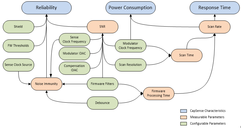
Reliability
The following factors affect reliability:
Signal-to-noise ratio (SNR)
: SNR gives a measure of confidence in a valid touch signal. For reliable CAPSENSE™ operation, it should be greater than 5. Manual tuning can ensure optimal SNR in specific designs
Noise immunity: It is the ability of the system to resist external or internal noise. Typical examples of external noise are ESD events, RF transmitters such as Bluetooth® LE, switching relays, power supply, and so on. The internal noise source could be an LED driven by PWM, or I 2 C, or SPI communications for example. Even designs with good SNR may suffer from poor performance because of poor noise immunity. Manual tuning allows to tune frequencies and parameters to help avoid noise interference by allowing more control over selection of different parameters
Power consumption and response time
The following factors affect the power consumption and response time:
Scan rate: Scan rate can be defined as the frequency at which you scan the sensor. Scan rate decides the minimal possible time from the finger touch until it is reported. The maximum scan rate will be limited by the Sensor scan
Scan time: It is the time taken to scan and process a particular sensor. It affects power consumption as indicated in Low-power design and scan rate as indicated above. Manual tuning can achieve specific scan durations while maintaining a minimum SNR
Firmware touch delay: This can be caused by the Debounce procedure or use of Raw Data Noise Filters depending on the CAPSENSE™ component version you are using). Both affect scan time by adding to the processing time of a sensor and delay the touch reporting until a certain number of samples in a row show the touch signal. In both cases response rate is reduced, but reliability is usually improved
Tuning debug FAQs
This section lists the general debugging questions on CAPSENSE™ Component tuning. Jump to the question you have, for quick information on possible causes and solutions for your debugging topic.
The tuner does not communicate with the device
Cause 1:
Your device is not programmed.
Solution 1: Make sure to
Program
your device with your latest project updates before launching the tuner.
Cause 2:
The tuner configuration setting does not match the SCB Component setting.
Solution 2: Open the EzI2C slave component configuration window, that is, the Configure ‘SCB_P4’ dialog and verify that the settings match the configuration of the Tuner Communication Setup dialog. See the
CAPSENSE™ Component datasheet
for details on tuner usage.
Cause 3:
Your I2C pins are not configured correctly.
Solution 3: Open the
.cydwr
file in Workspace Explorer and ensure the pin assignment matches what is physically connected on the board.
Cause 4:
You did not include the CAPSENSE™ TunerStart API or another required tuner code.
Solution 4: Add the tuner code listed in
CAPSENSE™ Component
datasheet to your main.c and reprogram the device.
I am unable to update parameters on my device through the tuner
Cause 1:
Your communications settings on the device are incorrect.
Solution 1: Review and make sure the settings in the UART/EZI2C configurator dialog and Tuner Communication Setup dialog match. Make sure that the sub-address size is equal.
I can connect to the device but I do not see any raw counts
Cause 1:
You did not add the tuner code to your project.
Solution 1: Review the
Tuner GUI
section and add the tuner code to your main.c and reprogram the device.
Difference counts only change slightly (10 to 20 counts) when a finger is placed on the sensor
Cause 1:
The gain of your system is too low.
Solution 1: Review the
Tuner GUI
section of this document.
Cause 2:
Your sensor parasitic capacitance is very high.
Solution 2: To confirm this issue, use the Built-in Self-Test (BIST) APIs documented in the
Component datasheet
. These functions allow you to read out an estimate of the sensor parasitic capacitance. You can also confirm this reading independently with an LCR meter.
If your hardware has an option to enable
Driven shield signal and shield electrode
, use this option in the advanced settings of the CAPSENSE™ Component configuration window. A driven shield around the sensors helps reduces the parasitic capacitance. When you enable this option, you may want to enable driving the shield to unused sensors by also changing the “Inactive Sensor connection” setting to “shield” in the advanced settings. If after enabling the shield, your
C
P
remains greater than the supported range of parasitic capacitance by the PSOC™ device, review your board layout to reduce
C
P
further, by following the PCB layout guidelines, and/or contact
Technical support
to review your layout. See
Component datasheet/middleware document
for more details on the supported range of
C
P
Cause 3:
Your overlay may be too thick.
Solution 3: Review your
Overlay thickness
with respect to your
Overlay thickness
.
Cause 4:
Raw counts may be too close to saturation and hence, saturating when sensor is touched.
Solution 4: Tune IDAC to ensure that raw counts are tuned to ~85 percent of the max raw count for a given sensor according to the
Modulation and compensation IDACs
section.
After tuning the system, I see large amount of radiated noise during testing
Cause 1:
The sense clock frequency is causing radiated noise in your system.
Solution 1: Reduce the sense clock frequency or enable PRS for your sensor based on
Electromagnetic compatibility (EMC) considerations
section. If it is already enabled, see the
Electromagnetic compatibility (EMC) considerations
section.
Cause 2:
Large shield electrode may be contributing to a large radiated noise.
Solution 2: Reduce the size of shield electrode based on
Layout guidelines for liquid tolerance
.
My scan time no longer meets system requirements after manual tuning
Cause:
The noise and
C
P
of your system are high, which requires more scan time and filtering to achieve reliable operation.
Solution:
C
P
needs to be reduced. First, enable the
Driven shield signal and shield electrode
in the advanced settings of the CAPSENSE™ Component configuration window and ensure gain is set as high as possible by reviewing the
PCB layout guidelines
. If your system still cannot meet final requirements, you may need to change your board layout to reduce
C
P
further, review the
PCB layout guidelines
for the same.
I am unable to calibrate my system to 85 percent
Cause 1:
Your sensor may have a short to ground.
Solution: First, use a multimeter to check if there is a short between your sensor and ground. If it is present, review your schematic and layout for errors.
Cause 2:
Your sensor
C
P
may be too high or too low.
Solution: If your hardware has an option to enable
Driven shield signal and shield electrode
, use this option in the advanced settings of the CAPSENSE™ Component configuration window. A driven shield around the sensors helps reduces the parasitic capacitance. If you do not have a hardware option to use shield or if after enabling the shield, your
C
P
remains greater than the device supported
C
P
, contact
Technical support
to review your layout or for further application-specific guidance.
If you suspect the capacitance to be low compared to the minimum supported parasitic capacitance by the device, add a footprint of the capacitor to a pin. In the final design, if the
C
P
is identified to be lower than the supported range, place an additional compensation capacitor to increase the sensor
C
P
to the supported range by dynamically connecting it to the sensor while scanning. See the
Component datasheet/middleware document
to understand how to gang the sensors to an external compensation capacitor connected to a pin to increase the
C
P
whenever required.
Figure 174. Gang the sensors to the external compensation capacitor
My slider centroid response is non-linear
Cause:
Layout may not meet hardware design guidelines to ensure proper linearity.
Solution: Check the
C
P
of the sensors using the built-in self-test option in the General tab of the CAPSENSE™ configuration window and update the layout according to the
Slider design
section. See the
Component datasheet/middleware document
section for details on BIST API.
My slider segments have a large variation of CP
Cause:
Your layout design caused your sensors to have an unbalanced
C
P
.
Solution: Your layout needs to be updated. Review
Slider design
and update your layout as required. If this is not immediately possible, you should re-tune every sensor to have a similar response. This will be a long iterative process and the preferred method is to update the hardware, if possible.
Raw counts show a level-shift or increased noise when GPIOs are toggled
Cause 1:
The sensor traces are routed parallel to the toggling GPIOs on your PCB.
Solution: Your layout needs to be updated. Review
Trace routing
and update your layout as required. If the layout cannot be modified at the current stage, you could evaluate the use of firmware filters to reduce the peak-to-peak noise and hence improve SNR.
Cause 2:
A large amount of current is being sinked through the GPIOs.
Solution: Limit the amount of DC current sink through the GPIOs when CAPSENSE™ sensors are being scanned. See
Schematic rule checklist
. If the current sink through GPIOs is firmware-controlled, and the raw count-level-shift caused by current sink has a large difference compared to the touch signal, you could implement firmware techniques like resetting or re-initializing the CAPSENSE™ baseline whenever the current sink is enabled through the GPIOs. The baseline of the CAPSENSE™ sensor could be reset by using the
CapSense_InitializeWidgetBaseline()
API function as shown below:
CapSense_InitializeWidgetBaseline(CapSense_CSD_BUTTON_WDGT_ID);
Figure 175. Resetting baseline using firmware technique
Cause 3:
You did not follow the guidelines mentioned in
Sensor pin selection
section.
Solution: Follow the recommendations in
Sensor pin selection
section. In addition, for PSOC™ 6 family of devices, follow these guidelines on drive mode strength, switching frequency and slew rate selection, and so on:
Reduce the drive strength of the switching GPIOs. Table 25 lists the available drive strength options for the GPIOs. Figure 176 shows an example on how to select the drive strength of the GPIOs using the Device configurator in the ModusToolbox™ project
Drive strength | Drive current in mA |
|---|---|
Full | 8 |
4 | |
2 | |
1 |
Decrease the switching frequency of the GPIO being toggled
Use GPIO slew rate as SLOW mode (note that this limits the toggling frequency to 1.5 MHz). See Table 43 for more details
Use PRS as the Sense clock source.
If possible, reduce VDDA to lower than 2.7 V
Try to restrict GPIO switching to intervals between CAPSENSE™ scans
Figure 176. Selecting drive strength for GPIOs
I am getting a low SNR
Cause 1:
Sensor is not tuned properly.
Solution: Follow the tuning guidelines in CAPSENSE™ performance tuning .
Cause 2:
CAPSENSE™ and other peripherals are not properly assigned to the recommended pin.
Solution: See
Sensor pin selection
and
Raw counts show a level-shift or increased noise when GPIOs are toggled
for more details.
Cause 3:
HFCLK source may be causing higher noise for a PSOC™ 6 device.
Solution: For the best performance of CAPSENSE™ in PSOC™ 6 family of devices, use HFCLK derived from the IMO/ECO+PLL clock source. This clock source provides the best SNR performance.
Figure 177
shows how to change the clock settings using the System tab in the
Device configurator
for a ModusToolbox™ project. See
AN221774 - Getting started with PSOC™ 6 MCU
for more details on changing the device clock.
Figure 177. Changing clock settings in device configurator
I am observing a low CM for my CSX button
Cause:
The mutual capacitance between the Tx and Rx electrode should be higher than approximately 750 fF for proper IDAC calibration.
Solution: It is recommended to have two free pins in your device with footprint to add extra Capacitance if
C
M
of the button turn out to be low. We could then increase the sensor
C
M
to the supported range by dynamically connecting external capacitor to the CSX sensor while scanning as shown in the below figure, where Pin1 is ganged to the Tx pin and Pin2 is ganged to the Rx pin of the sensor respectively. This will help in mitigating low
C
M
risk if it is found during testing phase. See
Component datasheet/middleware document
to understand how to gang the sensor.
shows the addition of the external capacitor as a button widget in the CAPSENSE™ component and assigning dedicated pins to the Tx and Rx electrode.
Figure 179
shows the ganging of the sensor to the external capacitor by assigning Selected pins to both sensor pin and external capacitor pin, this must be done for both Rx and Tx electrode. There is no need to scan the external capacitor while scanning of the widgets, thus we can selectively scan widgets using the
APIs CapSense_SetupWidget()
and
CapSense_Scan()
provided by the CAPSENSE™ component.
Figure 178. Ganging external capacitor to increase the CM of the sensor
Figure 179. Assigning dedicated pins to the external capacitors
Figure 180. Gaining the external capacitor and sensor pin
Gesture in CAPSENSE™
Touch gesture support
The CAPSENSE™ Component in PSOC™ 4 and PSOC™ 6 MCU supports the gesture detection feature for button, sliders and touchpad widgets. It allows to identify different predefined gestures based on touch patterns on button, sliders and touchpad widget.
Note: The gesture detection feature is available for selected device part numbers. If you intend to use the gesture feature of the component, ensure that you select the device that supports this feature.
Gesture groups
Gestures are divided into several groups: Click, one-finger scroll, two-finger scroll, two-finger zoom, one-finger edge swipe, one-finger flick, and one-finger rotate.
lists the gestures supported by various widgets. See
Component datasheet/middleware document
for more details on how these gestures are defined and the parameter that to be configured in the CAPSENSE™ configurator to detect these gestures.
Widget type | Gesture groups | ||||||
|---|---|---|---|---|---|---|---|
Click | One-finger scroll | Two-finger scroll | One-finger flick | One-finger edge swipe | Two-finger zoom | One-finger rotate | |
Button | ✓ | – | – | – | – | – | – |
Linear slider | – | ✓ | – | ✓ | – | – | – |
Radial slider | ✓ | – | – | – | – | – | – |
Matrix buttons | – | – | – | – | – | – | |
Touchpad | ✓ | – | – | ✓ | – | – | ✓ |
Proximity | – | – | – | – | – | – | |
One-finger gesture implementation
Implementing gesture detection involves following steps:
Tuning the widget
Tune the CAPSENSE™ hardware and software parameters for the widget. Generally, in a gesture application, because of the speed and orientation of the finger movement changes, the finger may make a very little contact with the widget. This could be confirmed by viewing the centroid data in the
Tuner GUI
when the gesture is being performed. If the sensitivity is good enough, you will get the data without any break. If you observe any break in the centroid data, increase the sensitivity until the data for the gesture is complete and appear without any break.
Ensure that you get a SNR above 5:1 for the slight finger contact that you may want to detect. Also, ensure that you have a linear centroid response with respect to the finger position on the slider or touchpad. Tune the sensors using guidelines in section
Slider widget tuning
tuning for achieving the same
Selecting predefined gesture
First, enable Gestures in the Gesture tab in CAPSENSE™ Component. All gesture-related configuration parameters appear after enabling gestures; these parameters are systematically arranged by widgets/gesture groups as
Table 26
shows. According to the application requirement, you can enable and disable gestures by selecting the specific checkbox. Do the following to enable gestures and configure the corresponding parameters.
Select the widget for which gesture feature must be enabled in the Widget pane. If you have multiple widgets in the project, the PSOC™ Creator allows gesture recognition only one widget. However, in ModusToolbox™, gesture recognition can be enabled on more than one widget
Select the desired gestures in Gestures pane. User has an option to select multiple gestures. In PSOC™ Creator, you cannot enable scroll gesture and flick gesture at the same time. This is applicable for both sliders and touchpad. However, in ModusToolbox™, you can enable more than one gesture according to the application requirement
Configure all parameters in the Parameter pane. When a gesture is selected, the right pane of the window dispays the parameters of the selected gesture group. See the Component datasheet/middleware document
Figure 181. Configuring gestures in CAPSENSE™ component
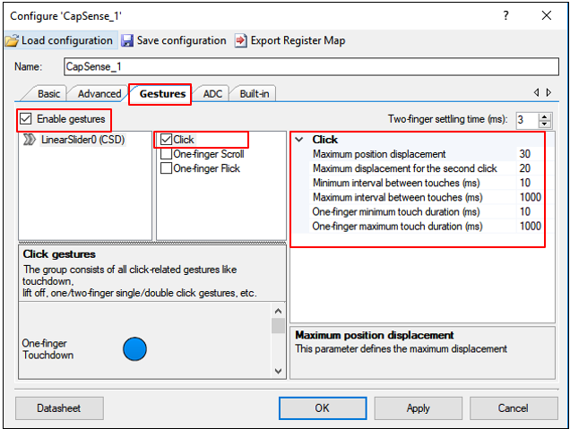
Firmware implementation with timestamp
See the code example
PSOC™ 4 CAPSENSE™ Touchpad Gestures
to understand how to implement timestamp for gesture recognition. Because each gesture has a pattern of touch that changes with time, a reference timestamp is needed for properly getting the touch data with respect to time. This time stamp represents the sampling rate for the gesture recognition algorithm. Both the centroid positions and their respective timestamp are used by the gesture decoding API to determine different predefined gesture patterns that are applicable for the widget.
First, tune the widget using the procedure described in
Tuning the widget
and determine the time interval between two successive CAPSENSE™ scans in the firmware. Update the timestamp exactly with this duration. The way to accurately determine it is to toggle a GPIO in the firmware after the CAPSENSE™ scan is complete and find the time duration using an oscilloscope.
Tuning gesture parameters
This section describes how to set gesture parameters for sliders; the same procedure could be extended to the gesture groups supported by touchpads. CAPSENSE™ sliders support Click, One-finger Scroll, and One-finger flick gesture features. See the
Component datasheet/middleware document
.
Using tuner GUI for tuning gesture parameters
You can use the
Gesture View
in
Tuner GUI
for tuning the gesture parameters and visualize and analyze the performance of the gesture detected in the end system.
Ensure the following while using Tuner GUI for gestures:
For tuning gesture parameters in runtime, Tuner GUI must be used with EZI2C. Use Synchronized communication mode for visualizing the detected gestures in runtime. For more details on using the Tuner GUI , see the Component datasheet/middleware document and the PSOC™ 4 CAPSENSE™ touchpad gestures code example . All the parameters for the gestures that are available in the CAPSENSE™ configurator are available in Tuner GUI , where you can directly edit these values for tuning.
As Figure 182 shows, the Gesture View tab is organized into different panes as follows:
Gesture Event History
pane shows detected gestures and their positions on the widget.
Detected Gesture
pane indicates the detected gesture. If the delay checkbox is enabled, a gesture picture is displayed for the specified time-interval; if delay is disabled, the last reported gesture picture is displayed until a new gesture is reported.
Cypress® Icon
in the Tuner GUI moves according to the scroll gesture. It indicates how well the parameter of the scroll gesture is tuned. This dynamic feature gives performance feedback for further fine-tuning gesture parameters.
Figure 182. Tuner GUI for gestures
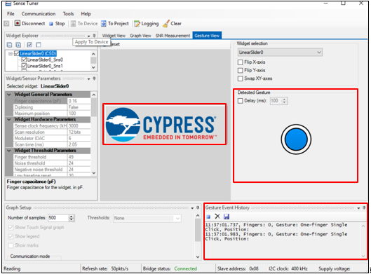
Determining the event duration using Tuner GUI . A general equation to determine the event duration is given by Figure 183 .
Figure 183. Gesture duration
Where,
= Number of samples the gesture event occurred. This data could be obtained from the Graph View in the Tuner GUI.
= Time interval between two samples.
Figure 184. Determining the Gesture parameters using Tuner GUI
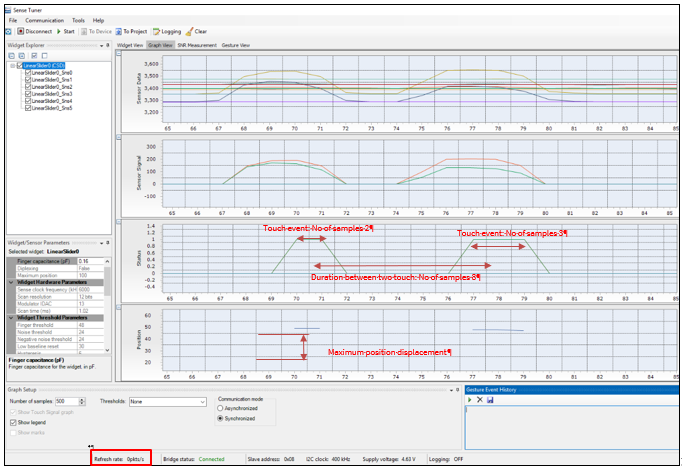
Click
There are two type of click gestures: single-click and double-click.
Table 27
lists the parameters to be configured for the Click
gesture
in both PSOC™ Creator and in ModusToolbox™. See
Component datasheet/middleware document
.
Table 28
provides the recommended values of the gesture parameter for the Click gesture.
Gesture | PSOC™ Creator | ModusToolbox™ |
|---|---|---|
Single-click | One finger minimum touch duration | Minimum click timeout |
One finger maximum touch duration | Maximum click timeout | |
Maximum position displacement | Maximum click distance | |
Double-click | Minimum interval between touches | Minimum second click interval |
Maximum interval between touches | Maximum second click interval | |
Maximum displacement for the second click | Maximum second click distance |
Parameters | Typical values |
|---|---|
Maximum position displacement | 20% of maximum position of the slider |
Maximum position displacement for the second click | 20% of maximum position of the slider |
Minimum interval between touches (ms) | 60 |
Maximum interval between touches (ms) | 400 |
One finger minimum touch duration (ms) | 20 |
One finger maximum touch duration (ms) | 400 |
Single click
A single click is defined as a touch-down event followed by a lift-off.
Figure 185
shows the spatial and timing condition that must be satisfied for a valid single-click event.
Figure 185. Single-click gesture
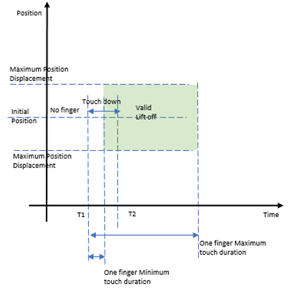
From
Figure 185
, at time T1, the finger touched down on the slider; at time T2, the finger is lifted off from the slider. For a valid single click, the touch-down duration should be between the “One finger minimum touch duration” and “one-finger maximum touch duration” and the relative position of the liftoff from the initial position of touch should be less than the “Maximum position displacement” parameter.
The duration of each single-click event can be determined by using
Figure 183
by finding the number of samples for the single click in the
Graph
view of
Tuner GUI
and the refresh rate as shown in
Figure 184
. From the single-click event duration, fix the parameters “One-finger minimum touch duration” and “One-finger maximum touch duration”. The maximum position displacement parameter can be determined by observing the maximum variation in the centroid position using the
Tuner GUI
as shown in
Figure 184
. The recommended value is 20 percent of the maximum centroid position of the slider as mentioned in
Table 27
.
Double click
A double click is two single-clicks event occurring one after another with the second click occurring between the minimum and maximum time interval between the two touches. In addition, the relative position of the second click from the initial position of touchdown event should be less than the maximum position displacement for the second click.
Figure 186
shows the spatial and timing conditions that must be satisfied for a valid double-click event.
Figure 186. Double-click gesture
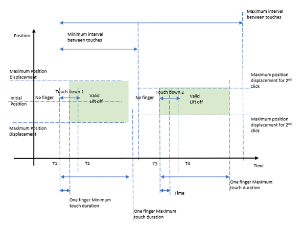
From
Figure 186
, at time T1, the finger touched down on the slider for the first click; at time T2, the finger is lifted off from the slider. At T3, the finger touched down on the slider for the second click; at T4, the finger is lifted off from the slider. For a valid double click, each click should satisfy the condition of single click, and the second click should occur between Minimum and Maximum interval between touch parameters.
Using the
Graph
view in the
Tuner GUI
, observe the double-click touch data. Determine the parameter of single click as mentioned in the
Single click
section. Determine the duration between the two touches using the Graph view in the
Tuner GUI
and set the value of the minimum and maximum intervals between touch parameters. A typical captured data for the double-click event is shown in
Figure 184
.
Scroll
There are two different scroll gestures that can be detected on sliders: One-finger scroll and One-finger Inertial scroll. See Component datasheet/middleware document. Table 29 shows the parameters to be configured for the scroll gesture.
Note: One-finger Inertial Scroll gesture is not supported in ModusToolbox™.
Gesture | PSOC™ Creator | ModusToolbox™ |
|---|---|---|
One-finger scroll | Position threshold N | Minimum scroll distance |
Scroll step | - | |
Debounce | Scroll debounce | |
One-finger inertial scroll | Position inertial threshold | NA |
Count level |
One-finger scroll
A One-finger Scroll gesture is a combination of a touchdown followed by a displacement in specific direction. The change in position between two consecutive scans must exceed the Position Threshold value given in the configurator after tuning. See
Component datasheet/middleware document
.
Follow these steps to set the scroll gesture parameter values as shown in
Table 29
.
Determine the number of samples of the scroll gesture from the Graph view (Centroid position) in Tuner GUI
By using Figure 183 determine the duration of the complete scroll
Determine the change in centroid position for the complete scroll using the Tuner GUI
Determine Position Threshold Figure 187 . Each gesture is scanned at a sample rate that is set in the timestamp in the application code. The position threshold is given by the change in the centroid position for the duration that is set in the timestamp
Figure 187. Equation to determine position threshold
In PSOC™ Creator, set four different position thresholds and their scroll count values in the configurator, which are determined by varying the speed of the scroll gesture. Now, change the speed of scroll and repeat the steps 1 – 4 and set these position threshold values. In ModusToolbox™ has only one parameter: Minimum Scroll distance; determine its value in the same way you determined the position threshold
Read the scroll step from the CAPSENSE™ data structure and use it to control the speed and smoothness of the scroll gesture. The scroll step depends on the position threshold. This scroll step is used in the application code to control the actual variable value to be changed with respect to scroll.
Note: The scroll step parameter is not available in ModusToolbox™.
Set the maximum slider position as ten times the dimension of the slider as a general rule. If you set scrollDistanceMin=10, everything below a 1-mm movement will not detect the scroll gesture. Everything above this number might detect a gesture
Observe the
Cypress®
icon in the Tuner GUI (see
Figure 182
) to get a feedback on how well the tuning has been done for the scroll gesture in the given hardware. You can also print the variable that must be controlled by scroll through UART to visualize how the value is changing with respect to scroll. This could be used as a visual feedback. The position threshold parameters and the corresponding step counts should be tuned until the variation in the variable value with respect to scroll meet the requirement of the end user application.
One-finger inertial scroll
The one-finger Inertial scroll gesture is defined as a touchdown event followed by a minimum displacement in a specific direction, and then a liftoff. The movement of scroll will automatically stop when it reaches the end value of the variable. See
Component datasheet/middleware document
.
The gesture parameter is provided in
Table 29
. The position inertial threshold parameter is given by the minimum change in centroid position that is required before a liftoff; its value can also be determined by steps in the
One-finger scroll
section. The count value parameter defines the momentum of scroll; it can take two possible values: low or high. Choose the count value according to the end application requirement.
One-finger flick
A flick gesture is a touchdown event followed by a high-speed displacement and a liftoff event (see
Component datasheet/middleware document
). The flick gesture is similar to the One-finger Inertial Scroll; the only difference is that it requires a high-speed displacement followed by a liftoff event within the maximum sample interval defined in the configurator. You can determine the position threshold and the maximum sample interval by following the same procedure in
One-finger scroll
section and by using
Figure 183
.
Gesture | PSOC™ Creator | ModusToolbox™ |
|---|---|---|
One Finger Flick Gesture | Position threshold | Minimum flick distance |
Maximum sample interval | Maximum flick timeout |
Two-finger gesture implementation
Two-finger gestures such as Two-finger Scroll and Two-finger Zoom are supported in the touchpad widget. You must enable this feature in the
Widget Details
tab of the Touchpad Widget. The procedure for tuning the parameters is the same as mentioned in the
One-finger gesture implementation
section (see
Component datasheet/middleware document
).
Figure 188
shows how to enable two-finger touch gestures in the configurator, select the centroid type as
5 x 5 Centroid
, and set the two-finger detection as
True
.
Figure 188. Enabling two-finger touch gestures in the CAPSENSE™ component
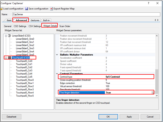
Advanced filters for gestures
Advanced filtering features for gestures such as Ballistic multiplier, Adaptive IIR filter, and the Edge correction feature are available to improve gesture recognition and the user experience.
See
Component datasheet/middleware document
.
Design considerations
This chapter explains the firmware and hardware design considerations for CAPSENSE™.
Firmware
The CAPSENSE™ component provides multiple application programming interfaces to simplify firmware development. The CAPSENSE™ Component datasheet provides a detailed list and explanation of the available APIs. You can use the CAPSENSE™ Example projects provided in PSOC™ Creator or ModusToolbox™ to learn schematic entry and firmware development. See CAPSENSE™ design and development tools for more details.
The CAPSENSE™ scan is non-blocking in nature. The CPU intervention is not required between the start and the end of a CAPSENSE™ scan. Therefore, you can use CPU to perform other tasks while a CAPSENSE™ scan is in progress. However, note that CAPSENSE™ is a high-sensitive analog system. Therefore, sudden changes in the device current may increase the noise present in the raw counts. If you are using widgets that require high sensitivity such as proximity sensors, or buttons with thick overlay, you should use a blocking scan. Example firmware for a non-blocking scan is shown below.
/* Enable global interrupts */
CyGlobalIntEnable;

/* Start EZI2C component */
EZI2C_Start();

/*
* Set up communication data buffer to CapSense data structure to be
* exposed to I2C master at primary slave address request.
*/
EZI2C_EzI2CSetBuffer1(sizeof(CapSense_dsRam),
sizeof(CapSense_dsRam),
(uint8 *)&CapSense_dsRam);

/* Initialize CapSense component */
CapSense_Start();
/* Scan all widgets */
CapSense_ScanAllWidgets();

for(;;)
(
/* Do this only when a scan is done */
if(CapSense_NOT_BUSY == CapSense_IsBusy())
( /* Process all widgets */
 CapSense_ProcessAllWidgets();
 /* Scan result verification */
 if (CapSense_IsAnyWidgetActive())
  (
    /* Add any required functionality
       based on scanning result */
  )
  /* Include Tuner */
  CapSense_RunTuner();
  /* Start next scan */
  CapSense_ScanAllWidgets();
)
/* CPU Sleep */
CySysPmSleep();
)
)
You should avoid interrupted code, power mode transitions, and switching ON/OFF peripherals while a high-sensitivity CAPSENSE™ scan is in progress. However, if you are not using high-sensitivity widgets, you can use CPU to perform other tasks. You can also use low-power mode of PSOC™ to reduce the average power consumption of the CAPSENSE™ system, as explained in the next section. Monitoring and verifying the raw counts and SNR using the Tuner GUI is recommended if you are using a non-blocking code.
If you want to develop firmware using the ModusToolbox™ software, see the references in the
ModusToolbox™
section of this document.
Low-power design
PSOC™ low-power modes allow you to reduce overall power consumption while retaining essential functionality. See
AN234231 - Achieving lowest-power capacitive sensing with PSOC™ 4000T
and
AN86233 - PSOC™ 4 MCU low-power modes and power reduction techniques
, for a basic knowledge of PSOC™ 4 low-power modes. See
AN219528 - PSOC™ 6 MCU low-power modes and power reduction techniques
, for PSOC™ 6’s low-power modes, and
AN210998 - PSOC™ 4 low-power CAPSENSE™ design
, for designing a low-power CAPSENSE™ application.
The CPU intervention is not required between the start and the end of a CAPSENSE™ scan. If the firmware does not have any additional task other than waiting for the scan to finish, you can put the device to Sleep mode after initiating a scan to save power. When the CSD hardware completes the scan, it generates an interrupt to return the device to the Active mode.
There are different firmware and hardware techniques to reduce the power consumption of the CAPSENSE™ system.
If you use APIs that scan multiple widgets together, the device returns to Active mode after finishing the scan of a single widget. Therefore, you should scan each widget individually for reducing the power consumption in the design. See the CAPSENSE™ Component datasheet
You can use the Deep-Sleep mode of PSOC™ to considerably reduce the power consumption of a CAPSENSE™ design. However, the CAPSENSE™ hardware is disabled in the Deep-Sleep mode. Therefore, the device must wake up frequently to scan for touches. You can use the watchdog timer (WDT) in PSOC™ to wake up the device from the Deep-Sleep mode at frequent intervals. Increasing the frequency of the scans improves the response of the CAPSENSE™ system, but it also increases the average power consumption
As the number of sensors in the design increases, the device has to spend more time in the Active mode to scan all sensors. This, in turn, increases the average power consumption. For saving power in a design with multiple sensors, you should include a separate proximity loop that surrounds all the sensor. When the device wakes up from the Deep-Sleep mode, only scan this proximity sensor. If the proximity sensor is active, the device must stay in the Active mode and scan other sensors. If the proximity sensor is inactive, the device can return to the Deep-Sleep mode. Figure 189 illustrates this process
Figure 189. Low-power CAPSENSE™ Design
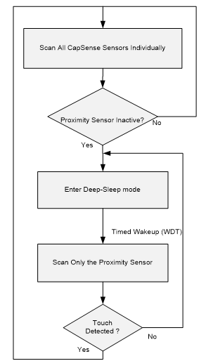
The CAPSENSE™ component can reduce power consumption by reducing the execution time of scanning by ganging sensors together and managing scanning at the application level. In this case, all the sensors in the design are “ganged” that is, simultaneously connected to the AMUX bus to form a virtual sensor. See the code example PSOC™ 4 low power ganged sensor and AN92239 - Proximity sensing with CAPSENSE™ for details on ganged sensor implementation. A ganged sensor has different tuning parameters because its properties are different compared to considering the sensors individually. Therefore, it should be considered as a single CSD button and tuned separately; see Manual tuning . The ganged sensor is periodically scanned by using a watchdog timer (WDT); if the ganged sensor reports a touch event, enable the scanning of the actual widgets that need to be scanned. This is helpful in CAPSENSE™ designs that requires Wake on Touch modes. The procedure is similar to what is explained in Figure 189 . You can achieve very low system current while maintaining a good touch response, by properly tuning CAPSENSE™ and the wakeup interval. This technique could also be used with the CSX touchpad widget
If high-speed peripherals such as system timers and I 2 C are required, you can put the CPU to sleep mode instead of going to deep sleep mode
You can also add a shield hatch in the design, as explained in Driven shield signal and shield electrode to reduce the parasitic capacitance and therefore, the scan time. The scan time and power consumption is directly related; thus, the power consumption is reduced by lowering the scan time
Note: In PSOC™ 4000 devices, it is not recommended to enter Sleep mode if a CAPSENSE™ scan is in progress.
Synchronized scanning
In Fifth-Generation Low-Power CAPSENSE™ (MSCLP), the sensor scanning can be controlled using the External Frame Start feature. This allows scanning to be triggered by a pulse on the External Frame Start pin (ext_frm_start). This feature is available in PSOC™ 4000T and PSOC™ 4100T Plus.
This feature can be used to synchronize the scanning of multiple devices with MSCLP on-board or to synchronize with external periodic noise sources, such as LCDs.
External frame start pulse guidelines
Mentioned below are the characteristics of the External Frame Start signal for the proper operation of the external frame start feature.
Scan trigger:
A scan will happen only when an external frame start signal is received after a scan_all_slots has been called in the application.
Figure 190. Scan trigger

Pulse Type:
A clean rectangle wave
Pulse Period:
The period of pulse that is interval between two subsequent pulses should not be lesser than the frame duration + MSC ISR duration + Processing duration
Figure 191. Pulse period

Minimum Pulse Width:
The pulse should not be shorter than 2 ILO cycles
Figure 192. Minimum pulse width

Max Pulse Width:
Should not be longer than scanning frame duration
Figure 193. Max pulse width

Sync interval (interval between the calling scan_all_slots() and the pulse):
Should be longer or equal 2 ILO cycles.
Figure 194. Sync interval

Conditioning the external frame start pulse
With the help of external frame start feature in MSCLP, scans can be synchronized with an LCD sync signal. If the external frame start signal does not comply with the guidelines mentioned in the
External Frame Start Pulse Guidelines
section, the signals will need to be conditioned. One way to condition the sync signal is using the TCPWM hardware present in the device. It receives the LCD sync signal (e.g., 60 Hz square wave) and generates the external_frame_start signal, with the appropriate width, as output.
Figure 195. Using TCPWM to generate conditioned pulse

The TCPWM is configured as a single shot timer. The timer gets triggered by an external input pulse. This external input pulse is the LCD sync signal, and the output from the TCPWM is fed to the ext_frm_start pin of the MSCLP.
Three GPIOs and 1 TCPWM are used in this approach,
External Trigger input for the TCPWM
TCPWM line output
MSCLP ext_frm_strt pin
The output from the TCPWM needs to be wired and connected to the input of the ext_frm_strt pin.
Sensor construction
A capacitive sensor can be constructed using different materials depending on the application requirement. In a typical sensor construction, a conductive pad, or surface that senses a touch is connected to the pin of the PSOC™ using a conductive trace or link. This whole arrangement is placed below a non-conductive overlay material and the user interacts on top of the overlay.
shows the most common CAPSENSE™ sensor construction.
Figure 196. CAPSENSE™ sensor construction
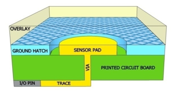
The copper pads etched on the surface of the PCB act as CAPSENSE™ sensors. A nonconductive overlay serves as the touch surface. The overlay also protects the sensor from the environment and prevents direct finger contact. A ground hatch surrounding the sensor pad isolates the sensor from other sensors and PCB traces.
If liquid tolerance is required, you should use a shield hatch instead of the ground hatch. In this case, drive the hatch with a shield signal instead of connecting it to ground. See
Liquid tolerance
section for details.
The simplest CAPSENSE™ PCB design is a two-layer board with sensor pads and hatched ground plane on the top, and the electrical components on the bottom.
Figure 197
shows an exploded view of the CAPSENSE™ hardware.
Figure 197. CAPSENSE™ hardware Sensor construction using springs as sensors
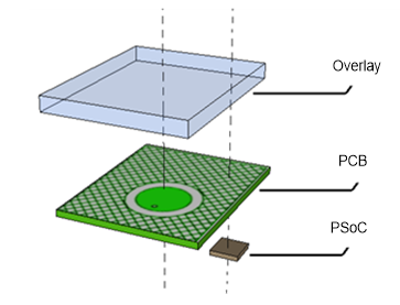
Sensors may also be constructed by using materials other than copper, such as indium tin oxide (ITO) or printed ink on substrates such as glass or a flex PCB. In some cases, springs can also be used as CAPSENSE™ sensors as
Figure 198
shows, to create elevated sensors that allow overlay to be placed at an elevated distance from the PCB. See
Getting started with CAPSENSE™ design guide
for PCB design considerations specific to spring sensors and other non-copper sensors such as ITO and printed ink.
Figure 198. Sensor construction using springs as sensors
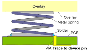
Overlay selection
Overlay material
The overlay is an important part of CAPSENSE™ hardware as it determines the magnitude of finger capacitance. The finger capacitance is directly proportional to the relative permittivity of the overlay material. See
Finger capacitance
for details.
shows the relative permittivity of some common overlay materials. Materials with relative permittivity between 2.0 and 8.0 are well suited for CAPSENSE™ overlay.
Material | εr |
|---|---|
Air | 1.0 |
Formica | 4.6 – 4.9 |
Glass (Standard) | 7.6 – 8.0 |
Glass (Ceramic) | 6.0 |
PET film (Mylar®) | 3.2 |
Polycarbonate (Lexan®) | 2.9 – 3.0 |
Acrylic (Plexiglas®) | 2.8 |
ABS | 2.4 – 4.1 |
Wood table and desktop | 1.2 – 2.5 |
Gypsum (Drywall) | 2.5 – 6.0 |
In capacitive touch sensing, the finger and the sensor behave as the two plates of a capacitance, with the overlay forming the dielectric material. Hence, in case of multiple overlays, it makes two capacitors in series. Thus, the effective dielectric constant is as shown below for two overlays of dielectric constant of ε1 and ε2 and thickness of d1 and d2.
Figure 199. Effective Dielectric constant for multiple overlays
Note: Conductive materials interfere with the electric field pattern. Therefore, you should not use conductive materials for overlay. You should also avoid using conductive paints on the overlay.
Overlay thickness
Finger capacitance is inversely proportional to the overlay thickness. Therefore, a thin overlay gives more signal than a thick overlay. See
Finger capacitance
for details.
lists the recommended maximum thickness of acrylic overlay for different CAPSENSE™ widgets.
Widget | Maximum thickness (mm) – 4th Generation CAPSENSE™ | Maximum thickness (mm) – 5th Generation CAPSENSE™ |
|---|---|---|
Button | 5 | 18 |
Slider | 5 11 | 18 |
Touchpad | 0.5 | 3 |
Because
Finger capacitance
also depends on the dielectric constant of the overlay, the dielectric constant also plays a role in the guideline for the maximum thickness of the overlay. Common glass has a dielectric constant of approximately ε
r
= 8, while acrylic has approximately ε
r
= 2.5. The ratio of ε
r
/2.5 is an estimate of the overlay thickness relative to plastic for the same level of sensitivity. Using this rule of thumb, a common glass overlay can be about three times as thick as a plastic overlay while maintaining the same level of sensitivity.
In addition, avoid using very thin or no overlay. It is important to have a minimum overlay thickness in a CAPSENSE™ design for the following reasons:
An overlay provides protection from the environmental condition, prevents direct finger contact, and gives ESD protection. The overlay thickness should be small enough to give a good signal, and decided based on the button size and the strength to withstand ESD. See AN64846 - Getting started with the CAPSENSE™
For the CSD button, if there is no overlay the buttons will be over sensitive
For sliders, if there is no overlay, the raw count may saturate for the slider segments and may cause non-linear centroid response for slider. See Slider design
For the CSX sensor, it is recommended to have a minimum overlay thickness of 0.5 mm. If it is violated, sudden decrease in raw count is observed when a finger is placed on a sensor or a water drop falls on the Tx and Rx electrodes. See Effect of grounding
Overlay adhesives
The overlay must have a good mechanical contact with the PCB. Use a non-conductive adhesive film for bonding the overlay and the PCB. This film increases the sensitivity of the system by eliminating the air gap between the overlay and the sensor pads. Recommendation for the Adhesive to be used are mentioned below:
Adhesive selection:
3M™ Acrylic Adhesive 200 MP
is typically recommended for its superior adhesion, high shear strength, and transparency. These properties make it a top choice for bonding applications where a reliable, transparent, and uniform bond line is essential.
Surface compatibility:
For overlays with minimal surface irregularities, such as acrylic and glass, a thinner adhesive layer (approximately 60 microns)is recommended. This ensures a smooth, uniform bond without visible air gaps.
If the surfaces have minor irregularities, such as 3D printed enclosures or milled plastics, a slightly thicker adhesive layer (around 130 microns) can be used to accommodate the unevenness and to prevent air gaps, ensuring a more reliable and durable bond.
Temperature and environmental considerations:
These adhesives perform well in commercial-grade applications, maintaining functionality and adhesion under typical usage conditions.
It is vital to assess the shear strength of these adhesives at higher temperatures. Especially in automotive applications where exposure to higher temperatures (either continuous or short term) is common.
A few additional points to consider:
Mechanical load durability:
Ensure that the adhesive can withstand various mechanical loads, including shear and peel stresses, to verify the bond's reliability under real-world conditions.
Automotive standards compliance:
Ensure that the adhesive is compatible with the thermal and environmental demands, typical of automotive applications, covering temperature ranges, humidity levels, and exposure to chemicals.
CAPSENSE™ system compatibility:
For CAPSENSE™systems, consider the adhesive's electrical insulation properties and ensure that it does not interfere with the capacitive sensing performance. Conduct appropriate testing to verify the sensor's performance before and after adhesive application.
PCB layout guidelines
PCB layout guidelines help you to design a CAPSENSE™ system with good sensitivity and high
Signal-to-noise ratio (SNR)
.
Sensor CP
In a CAPSENSE™ system design, the
C
P
of the sensor must be within the supported range of the device. You can find the supported
C
P
range in the
Component datasheet/middleware document
. The main components of
C
P
are trace capacitance, sensor pad capacitance, and pin capacitance of the device. The pin capacitance is device-dependent (see the
Device datasheet
), so you can only design your sensor and trace capacitance to be able to meet the
C
P
criteria in the datasheet. The relationship between
C
P
and the PCB layout features is not simple.
C
P
increases with an increase in the sensor pad size and trace length and width, and with a decrease in the gap between the sensor pad and the ground hatch.
There are many ways to decrease the
C
P
:
Decrease the trace length and width as much as possible. Reducing the trace length increases noise immunity
Drive the hatch with a shield signal. See
Driven shield signal and shield electrode
Reducing the sensor pad size is not recommended because it also reduces the finger capacitance. In some special cases, such as small sensor pad and very small trace length due to placement of the sensor pad close to the device, there is a possibility of the sensor
C
P
to be lower than the supported minimum
C
P
by the device. In that case, add a footprint of the capacitor across the sensor or any unused pin. If the
C
P
is identified to be lower than the supported range, place a 4.7 pF capacitor across the sensor or on the unused pin and gang the capacitor during the CAPSENSE™ scan, refer to the FAQ
I am unable to calibrate my system to 85 percent
for more details. This will increase the
C
P
of the sensor to the supported range.
If the sensor
C
P
is very high due to long traces or because of a nearby ground, use the mutual-capacitance sensing method so that the sensitivity is not degraded because of the high
C
P
value. The sensitivity of the CAPSENSE™ sensor in a mutual-capacitance sensing method is independent of the sensor
C
P
.
Board layers
Most applications use a two-layer board with the sensor pads and the hatched ground planes on the top side and all other components on the bottom side. PCBs that are more complex use four layers.
FR4-based PCB designs perform well with board thickness ranging from 0.020 inches (0.5 mm) to 0.063 inches (1.6 mm).
Flex circuits work well with CAPSENSE™ too. You can use flex circuits for curved surfaces. All PCB guidelines in this document also apply to flex. You should use flex circuits with thickness 0.01 inches (0.25 mm) or higher for CAPSENSE™. The high breakdown voltage of the Kapton® material (290 kV/mm) used in flex circuits provides built in ESD protection for the CAPSENSE™ sensors
Button design
Self-capacitance button design
The self-capacitance button has a single electrode and can have different shapes and size as recommended below.
Shape: You should use circular sensor pads for CAPSENSE™ buttons. Rectangular shapes with rounded corners are also acceptable. However, you should avoid sharp corners (<90º) since they concentrate electric fields.
Figure 200
shows recommended button shapes.
Figure 200. Recommended button shapes
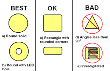
Size: Button diameter should be 5 mm to 15 mm, with 10 mm suitable for most applications. A larger diameter is appropriate for thicker overlays.
Spacing: The width of the gap between the sensor pad and the ground hatch should be equal to the overlay thickness, and range from 0.5 mm to 2 mm. For example, if the overlay thickness is 1 mm, you should use a 1 mm gap. However, for a 3 mm overlay, you should use a 2 mm gap.
Select the spacing between two adjacent buttons such that when touching a button, the finger is not near the gap between the other button and the ground hatch, to prevent false touch detection on the adjacent buttons, as
Figure 201
shows.
Figure 201. Spacing between buttons
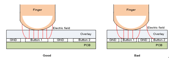
Mutual-capacitance button design
Mutual capacitance sensing measures the change in capacitive coupling between two electrodes. The sensor pattern should be designed in such a way that the finger disturbs the electric field between the Tx and Rx electrodes to a maximum extent. There are standard button patterns that could be used for the mutual capacitance button design and their parameters could be modified based on the application requirement. Fishbone pattern is one of the mutual capacitance patterns which give better performance in terms of SNR.
Fishbone pattern
Prongs or fishbone are standard shapes for mutual-capacitance buttons. The Tx forms a box or ring around the button for shielding Rx from noise. There are interlaced Tx and Rx prongs inside the border to form the electric field.
Figure 202
shows an example of a two-prong fishbone sensor structure with top and bottom view with hatched ground. The gap between the outer wall of the Tx electrode and the coplanar hatch ground should be greater than the air-gap of Tx and Rx electrodes. The reference plane (PCB bottom layer) of the Fishbone structure should have void region as shown in
Figure 202
.
Figure 202. CSX Fish bone button pattern with two Rx prongs
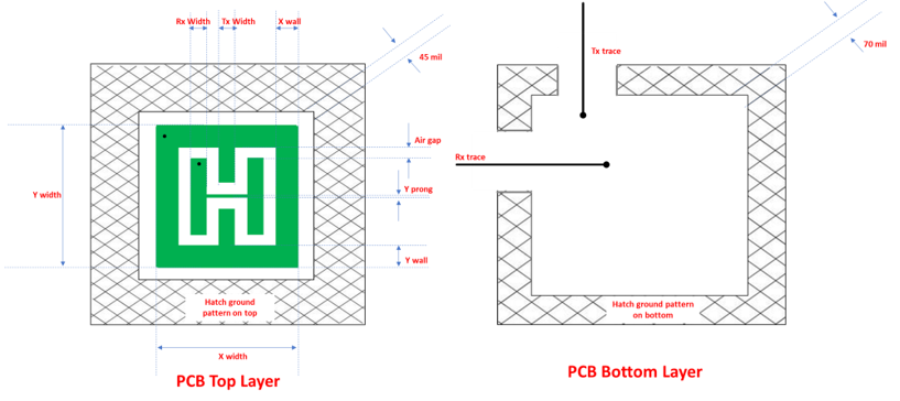
lists the suggested fishbone button design parameters for some commonly used sensor sizes and overlay like glass and acrylic. As explained in section
Sensor size
, the recommended button size is to keep the button X and Y dimension close to the sum of expected user finger size and overlay thickness. However, the table lists multiple button sizes that you can chose from if you have constraints on available space on board or if you would like to have a bigger button for your application for ease of user interaction etc.
Also, note that for a given button size, the achievable SNR decreases with increased overlay thickness. Thus, if you plan to use thick overlays (approx. > 1 mm acrylic or 2 mm glass) ensure to avoid compromising on button size due to board space because that will further limit the button SNR performance. Ensure to use bigger buttons (>= biggest expected finger size) for such thick overlays. And also, for small buttons better to have thin overlays for getting good SNR.
Button size (X-size, Y-size) (mm) | Number of Rx-prongs | Air gap between Tx and Rx in mm | Tx width in mm | Rx width in mm | X-wall wdth in mm | Y-wall width in mm | Y prong in mm |
|---|---|---|---|---|---|---|---|
5, 5 | 3 | 0.35 | 0.48 | 0.48 | 0.24 | 0.24 | 0.2 |
10,7 | 3 | 0.75 | 0.92 | 0.92 | 0.46 | 0.46 | 0.2 |
10,5 | 3 | 0.5 | 1.17 | 1.17 | 0.58 | 0.58 | 0.2 |
10,10 | 2 | 0.9 | 1.60 | 1.60 | 0.80 | 0.80 | 0.2 |
12, 12 | 2 | 1.3 | 1.70 | 1.70 | 0.85 | 0.85 | 0.2 |
13, 10 | 2 | 1.1 | 2.15 | 2.15 | 1.08 | 1.08 | 0.2 |
13, 13 | 2 | 1.5 | 1.75 | 1.75 | 0.88 | 0.88 | 0.2 |
15, 15 | 2 | 1.7 | 2.05 | 2.05 | 1.03 | 1.03 | 0.2 |
17, 17 | 2 | 2.3 | 1.95 | 1.95 | 0.98 | 0.98 | 0.2 |
20, 13 | 2 | 1.8 | 3.20 | 3.20 | 1.60 | 1.60 | 0.2 |
25, 13 | 2 | 2 | 4.25 | 4.25 | 2.13 | 2.13 | 0.2 |
The above button design parameters in
Table 33
ensure a good SNR performance if you follow the schematics and layout guidelines in this chapter.
Note: In case if you expect a higher external noise in the design and for other complex cases you can contactTechnical supportfor any assistance in the button design. Refer to the sectionNoise in CAPSENSE™ systemfor more details about the external noise. And in the design if you expect a lowCMthen follow the guidelines mentioned in the sectionI am observing a low CM for my CSX buttonfor mitigating it.
Button design for arbitrary shapes and dimensions
shows the different orientation of Rx prongs in the Fish bone pattern, in Button A the Rx prong is perpendicular to the side of the button with larger dimension and in Button B the Rx prongs is parallel to the side of the button with larger dimension. Orientation of Rx prongs like in Button A results in optimized button pattern compared to Button B. Thus, it is always recommended to have Rx prongs perpendicular to the side of the button with larger dimension. Thus if you need a 10x13 mm button, then simply use the 13x10 mm button from
Table 32
and rotate it 90º to get 13x10 mm
Noise in CAPSENSE™ system
button pattern as shown in
Figure 203
.
Figure 203. Orientation of Rx prongs
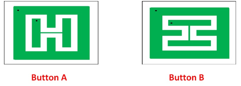
Figure 204. Rotating the button 90 deg to get the desired button dimension
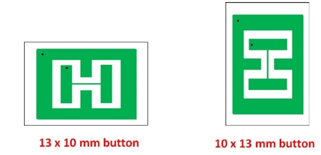
There may be some design where you need a different button shape than the recommended rectangular, like an oval or circular shape etc. The below steps explain how to construct the button with nonstandard shape from the standard Fish bone pattern.
First select the Fishbone pattern (Rectangular shape for oval shape and Square button for circular shape) from Table 32 to cover the desired button shape
Then in the user interface or above the overlay print button shape with required dimension over the fishbone pattern as shown in Figure 205
Mutual capacitance buttons designed using this method have some oversensitive area or less sensitive outside the button shape as shown in the below figures, this could be mitigated by properly tuning the software thresholds of the mutual capacitance button. The below figure shows an example of a circular button made using a square fishbone pattern.
Figure 205. Arbitrary shape button design based on arbitrary pattern

If you want a pattern that is not present in Table 32 , you can obtain the button parameters by following few steps. For example, if you want a 19x19 pattern, choose the pattern that is close to the required pattern from Table 32 like 17x17, and scale the air gap between Tx and Rx with respect to the button areas. For example:
Where, ButtonArea=X x Y dimension of the sensor.
Compute the Tx, Rx width and Tx wall based on the assumption below and by considering the
New
gap
as obtained above. The obtained values of the button design parameters are shown in
Table 33
. Refer to the
Figure 202
to understand the description of the button design parameters.
Button size (X-size, Y-size)(mm) | Number of Rx-prongs | Air gap between Tx and Rx in mm | Tx width in mm | Rx width in mm | X-wall width in mm | Y-wall width in mm | Y prong in mm |
|---|---|---|---|---|---|---|---|
17, 17 | 2 | 2.3 | 1.95 | 1.95 | 0.98 | 0.98 | 0.2 |
19,19 | 2 | 2.9 | 1.85 | 1.85 | 0.93 | 0.93 | 0.2 |
General recommendations on Fishbone pattern parameters
Sensor size
The sensor size is the XY dimension of the button, it is selected based on the board space availability, expected user finger size and overlay material and thickness. Sensor size selection also depends upon the number of required buttons on the PCB considering required button-to-button gap and space availability in the PCB. But if the space is not the constrain then choose higher button size which will result in getting a good SNR. Note that increasing the sensor size beyond a point will cause the SNR to saturate, this is because some of the electric field lines from Tx/Rx electrode do not interact with the finger as shown in
Figure 206
.
Figure 206. Interaction of electric filed with the finger
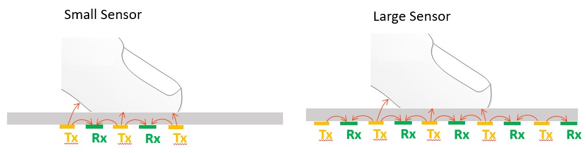
The SNR of the button is decreased with usage of thick overlays. Thus, the recommended minimum sensor size is finger size plus overlay thickness to achieve a good SNR even with thick overlays. For example, the minimum sensor size recommended could be 13x10 mm, considering the finger size around 10mm in diameter and 3 mm overlay thickness. As mentioned in the
Button design for arbitrary shapes and dimensions
Rx prongs should be perpendicular to the side with large dimension.
Button spacing
The button spacing is the gap between the Tx wall of two buttons. It helps to prevent user error by isolating the buttons from each other and reduces the cross talk. It is recommended to keep a minimum of 8 mm spacing between the buttons this will ensure a good single touch and multi touch performance.
Overlay
The overlay thickness and overlay permittivity influences the SNR of the button and immunity towards the external noise such as ESD. Refer to the
Overlay selection
section for more details. It is recommended to keep the overlay thickness as minimum as possible which will help in getting a higher SNR for the button and it should be high enough to provide immunity towards ESD noise. In some cases, if the overlay thickness is more and you cannot avoid it due to mechanical design consideration. In such a case, for getting a better SNR use a mutual capacitance button with bigger size than the recommended size. Refer to the section
Sensor size
for selecting the minimum button dimension with respect to the overlay thickness. Using an overlay material with higher dielectric constant will also leads to higher SNR. So always use material with high dielectric constant when we use thick overlay. And also, for smaller buttons better to have thin overlays for getting good SNR.
Air gap between Tx and Rx electrode
The gap between the Tx and Rx electrode influences the mutual capacitance between the Tx and Rx electrode. Increasing the gap reduces the mutual capacitance. It is the most critical parameter in the Fishbone pattern design and the gap between the Tx and Rx electrode such that the mutual capacitance is above 750 fF.
Number of Rx-prongs
The number of Rx prongs influence the mutual capacitance between the Tx and Rx electrode, because increasing the number of Rx prongs decreases the gap between the Tx and Rx electrode for a given button size. Higher mutual capacitance implies higher electric field lines between Tx and Rx electrode. Thus, we get a higher signal when we touch the button, because the finger touch will disturb the electric field to a maximum extent. But higher
C
M
also increases the impact of external noise such as VDDA ripple noise. Thus, there is a tradeoff in selecting the number of Rx prongs to get a higher signal verses getting good noise immunity. The optimal number of Rx prongs is 2 for the Fishbone pattern (that is Fishbone pattern with a single Tx prong and two Rx prongs). The below figure shows the mutual capacitance button with three and one number of Rx prongs.
Figure 207. Mutual capacitance button with different number of prongs
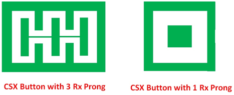
Tx electrode and Rx electrode width
The Tx electrode and Rx electrode width influences the mutual capacitance between Tx and Rx electrode. Best signal response is achieved when Rx width/area is equal to Tx width/area in the case of less external noise in the system. The below figure shows the electric filed lines from Tx to Rx electrode with equal and unequal widths. Thus, from the below figure it is clear that having equal Tx and Rx width will eventually leads to higher change in
C
M
for a finger touch.
Figure 208. Effect of Tx and Rx width
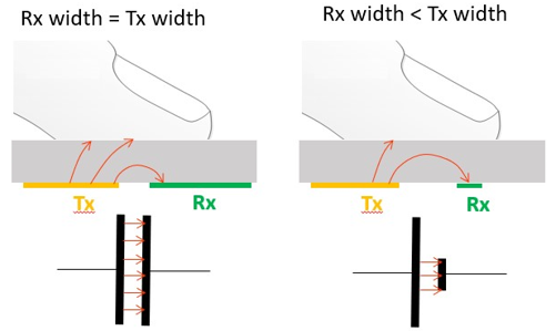
In some cases, it is required to provide liquid tolerance to the mutual capacitance button as mentioned in section
Liquid tolerance for mutual-capacitance sensing
. To achieve that we have to use a hybrid sensing technique with both CSX and CSD sensing method. In such a case the Tx or Rx electrode whichever is scanned in CSD technique should have a significant width so that it ensures a good signal for a finger touch.
Co planar ground
Presence of coplanar ground decreases the impact of noise in the system and it also provides good ground resulting in decreased signal disparity effect. It is recommended to have as much area surrounding the sensor with hatched pattern and connected it to device ground. Also follow the recommendations as mentioned in the layout and schematics guidelines in this chapter. Ground plane reduces the coupling of electric field lines to the approaching finger, which decreases the change in mutual capacitance caused by a finger touch. It is suggested to avoid having ground plane underneath the sensor unless you expect strong coupling to a noise source present right below the sensor. Figure 202 shows the coplanar ground on the top and bottom layer of the PCB. The gap between the outer wall of the Tx electrode and the coplanar hatch ground should be greater than the air-gap of Tx and Rx electrodes.
Tx wall (X-wall and Y-wall width)
Tx wall act as a shield to the Rx electrode from noise. Wide Tx wall also reduces the effect of cross talk and the impact of Co-planar ground. It is recommended to keep the Tx wall width approximately equal to half of Tx electrode width. The below figure shows the effect of wider Tx wall, it increases the number of electric field lines reaching the finger from the Tx electrode by reducing the impact of Coplanar ground. The width of Tx wall can also be slightly increased in case Tx electrode is scanned as a CSD sensor as mentioned in section
Liquid tolerance for mutual-capacitance sensing
. An example 10x10 pattern with increased Tx wall is given in
Table 34
.
Figure 209. Effect of width of Tx wall
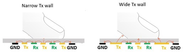
Button Size (X-Size, Y-Size) (mm) | Number of Rx-Prongs | Air Gap between Tx and Rx in mm | Tx Width in mm | Rx Width in mm | X-Wall Width in mm | Y-Wall Width in mm | Y Prong in mm |
|---|---|---|---|---|---|---|---|
10, 10 | 2 | 0.8 | 1.2 | 1.2 | 1.5 | 1.6 | 0.2 |
Slider design
shows the recommended slider pattern for a linear slider and
Table 36
shows the recommended values for each of the linear slider dimensions. A detailed explanation on the recommended layout guidelines is provided in the following sections.
Figure 210. Typical linear slider pattern
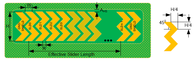
Parameter | Acrylic overlay thickness | Minimum | Maximum | Recommended |
|---|---|---|---|---|
Width of the segment (W) | 1 mm | 2 mm | - | 8 mm 12 |
3 mm | 4 mm | - | ||
4 mm | 6 mm | - | ||
Height of the segment (H) | - | 7 mm 13 | 15 mm | 12 mm |
Air gap between segments (A) | - | 0.5 mm | 2 mm | 0.5 mm |
Air gap between the hatch and the slider (A HS) | - | 0.5 mm | 2 mm | Equal to overlay thickness |
Slider-segment shape, width, and Air gap
A linear response of the reported finger position (that is, the centroid position) versus the actual finger position on a slider requires that the slider design is such that whenever a finger is placed anywhere between the middle of the segment SLD0 and middle of segment SLDn-1, other than the exact middle of slider segments, exactly two sensors report a valid signal
14
. If a finger is placed at the exact middle of any slider segment, the adjacent sensors should report a difference count = noise threshold. Therefore, it is recommended that you use a double-chevron shape as
Figure 210
shows. This shape helps in achieving a centroid response close to the ideal response, as
Figure 211
and
Figure 212
show. For the same reason, the slider-segment width and air gap (dimensions “W” and “A” respectively, as marked in
Figure 210
) should follow the relationship mentioned in
Figure 126
.
Figure 211. Ideal slider segment signals and centroid response
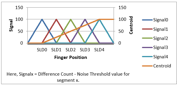
Figure 212. Ideal slider signals
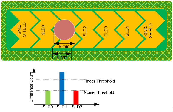
Figure 213. Segment width and air gap relation with the finger diameter
Typically, an average human finger diameter is approximately 9 mm. Based on this average finger diameter and
Figure 213
, the recommended slider-segment-width and air-gap is 8 mm and 0.5 mm respectively.
If the sum of
slider-segment width
and
2 * air-gap
is lesser than
finger diameter
, as required according to
Figure 213
, the centroid response will be non-linear. This is because, in this case, a finger placed on the slider will add capacitance, and hence valid signal to more than two slider-segments at some given position, as
Figure 214
shows. Thus, calculated centroid position in
Figure 215
will be non-linear as
Figure 216
shows.
Figure 214. Finger causes valid signal on more than two segments when slider segment width is lower than recommended
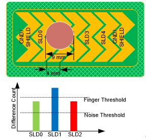
Figure 215. Centroid algorithm used by CAPSENSE™ component in PSOC™ Creator
Where,
Resolution = API resolution set in the CAPSENSE™ component customizer
n = Number of sensor elements in the CAPSENSE™ component customizer
x = Index of element which gives maximum signal
Si = Different counts (with subtracted noise threshold value) of the slider segment
Figure 216. Nonlinear centroid response when slider segment width is lower than recommended
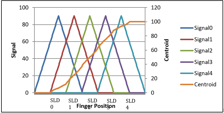
Note that even though a
slider-segment-width
value of less than
finger diameter – 2 * air-gap
provides a non-linear centroid response, as
Figure 216
shows; it may still be used in an end application where the linearity of reported centroid versus actual finger position does not play a significant role. However, a minimum value of slider-segment-width must be maintained, based on overlay thickness, such that, at any position on the effective slider length, at least one slider-segment provides a
Signal-to-noise ratio (SNR)
of ≥ 5:1 (that is signal greater than or equal to the finger threshold parameter) at that position. If the slider-segment width is too low, a finger may not be able to couple enough capacitance, and therefore, none of the slider-segments will have a 5:1 SNR, resulting in a reported centroid value of 0xFFFF
15
in PSOC™ Creator as
Figure 217
shows, and 0x0000
16
in ModusToolbox™.
Figure 217. Incorrect centroid reported when slider-segment-width is too low
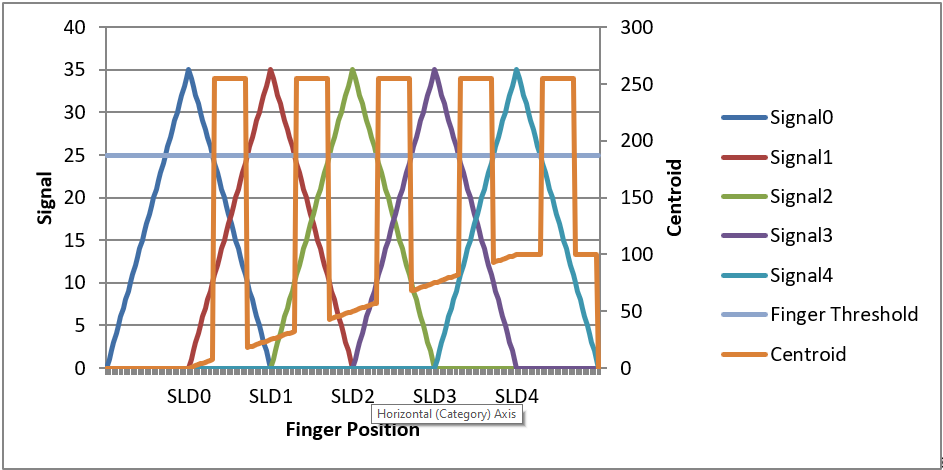
The minimum value of slider-segment width for certain overlay thickness values for an acrylic overlay are provided in
Table 36
. For thickness values of acrylic overlays, which are not specified in
Table 36
,
Figure 218
may be used to estimate the minimum slider-segment width. Very thin overlay or no overlay may cause a nonlinear centroid response due to saturation of raw count or due to high finger capacitance; centroid position may be detected before touching the slider. In these conditions, the CAPSENSE™ centroid algorithm will not be able to correctly estimate the finger position on the slider using
Figure 215
. It is recommended to have the overlay thickness for the CSD sensor as mentioned in
Table 35
.
Figure 218. Minimum slider-segment width with respect to overlay thickness for an acrylic overlay
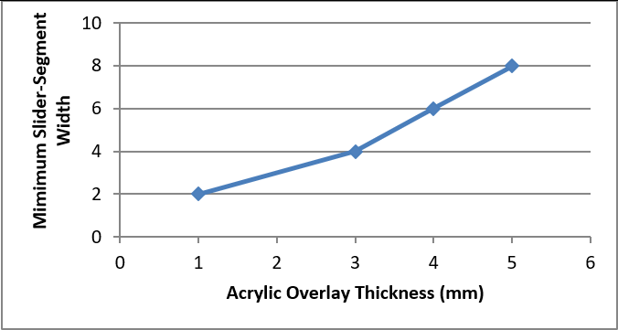
If the
slider-segment-width + 2 * air-gap
is higher than the
finger diameter
value as required in
Figure 213
, the centroid response will have flat-spots; that is, if the finger is moved towards the middle of any segment, the reported centroid position will remain constant as
Figure 219
shows. This is because, as
Figure 220
shows, when the finger is placed in the middle of a slider segment, it will add a valid signal only to that segment even if the finger is moved a little towards adjacent segments.
Figure 219. Flat-spots (nonresponsive centroid) when slider-segment width is higher than recommended
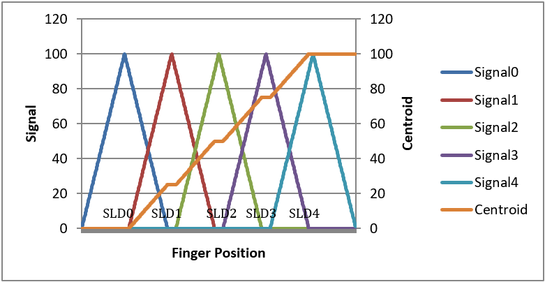
Figure 220. Signal on slider segments when slider-segment width is higher than recommended
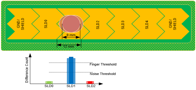
Note that if the value of
slider-segment-width + 2 * air-gap
is higher than the
finger diameter
, it may be possible to increase and adjust the sensitivity of all slider segments such that even if the finger is placed in the middle of a slider segment, adjacent sensors report a difference count value equal to the noise threshold value (see
Figure 211
); however, this will result in the hover effect – the slider may report a centroid position even if the finger is hovering above the slider and not touching the slider.
Dummy segments at the ends of a slider
In a CAPSENSE™ design, when one segment is scanned, adjacent segments are connected to either ground or to the driven- shield signal based on the option specified in the “Inactive sensor connection” parameter in the CAPSENSE™ CSD Component. For a linear centroid response, the slider requires all the segments to have the same sensitivity, that is, the increase in the raw count (signal) when a finger is placed on the slider segment should be the same for all segments. To maintain a uniform signal level from all slider segments, it is recommended that you physically connect the two segments at both ends of a slider to either ground or driven shield signal. The connection to ground or to the driven-shield signal depends on the value specified in the “Inactive sensor connection” parameter. Therefore, if your application requires an ‘n’ segment slider, it is recommended that you create n+2 physical segments, as
Figure 210
shows.
If it is not possible to have two segments at both ends of a slider due to space constraints, you can implement these segments in the top hatch fill, as
Figure 221
shows. Also, if the total available space is still constrained, the width of these segments may be kept lesser than the width of segments SLD0 through SLDn-1, or these dummy segments may even be removed.
If the two segments at the both ends of a slider are connected to the top hatch fill, you should connect the top hatch fill to the signal specified in the “Inactive sensor connection” parameter. If liquid tolerance is required for the slider, the hatch fill around the slider, the last two segments, and the inactive slider segments should be connected to the driven-shield signal. See the
Effect of liquid droplets and liquid stream on a self-capacitance sensor
section for more details.
Figure 221. Linear slider pattern when first and last segments are connected to top hatch fill
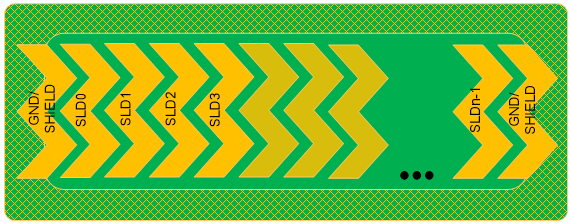
Deciding slider dimensions
Slider dimensions for a given design can be chosen based on following considerations:
Decide the required length of the slider (L) based on application requirements. This is same as the “effective slider length” as Figure 210 shows.
Decide the height of the segment based on the available space on the board. Use the maximum allowed segment height (15 mm) if the board space permits; if not, use a lesser height but ensure that the height is greater than the minimum specified in Table 36.
The slider-segment width and the air gap between slider segments should be as recommended in Table 36 . The recommended slider-segment-width and air-gap for an average finger diameter of 9 mm is 8 mm and 0.5 mm respectively.
For a given slider length L, calculate the number of segments required by using the following formula:
Figure 222. Number of segments required for a slider
Note: A minimum of two slider segments are required to implement a slider.
If the available number of CAPSENSE™ pins is slightly less than the number of segments calculated for a certain application, you may increase the segment width to achieve the required slider length with the available number of pins. For example, a 10.2 cm slider requires 13 segments. However, if only 10 pins are available, the segment width may be increased to 10.6 cm. This will either result in a nonlinear response as
Figure 219
shows, or a hover effect; however, this layout may be used if the end application does not need a high linearity.
Note: The PCB length is higher than the required slider length asFigure 210shows. PCB length can be related to the slider length as shown inFigure 223.
Figure 223. Relationship between minimum PCB length and slider length
If the available PCB area is less than that required per this equation, you can remove the dummy segments.
In this case, the minimum PCB length required will be as shown in
Figure 224
.
Figure 224. Relationship between minimum PCB length and slider length
Routing slider segment trace
A slider has many segments, each of which is connected separately to the CAPSENSE™ input pin of the device. Each segment is separately scanned and the centroid algorithm is applied finally on the signal values of all the segments to calculate the centroid position. The SmartSense algorithm implements a specific tuning method for sliders to avoid nonlinearity in the centroid that could occur due to the difference of
C
P
in the segments. However, the following layout conditions need to be met for the slider to work:
CP of any segment should always be within the supported range of CP as mentioned in the Component datasheet
C P of the slider segment should be as close as possible. However, in the practical scenario C P of each slider segment might vary because of differences in trace routing for each segment. The maximum allowed variation in the segment parasitic capacitance is 44% maximum CP of the slider segment for an 85% IDAC calibration level. If the variation in C P is beyond this limit then it may cause a change in the sensitivity among the slider segments leading to a non-linear slider response
Implement the following layout design rules to meet a good slider design with linear response.
Design the shape of all segments to be as uniform as possible
Ensure that the length and the width of the traces connecting the segments to the device are same for all the segments if possible
Maintain the same air gap between the sensors or traces to ground plane or hatch fill
Slider design with LEDs
In some applications, it may be required to display the finger position by driving LEDs. You can either place the LEDs just above the slider segments or drill a hole in the middle of a slider segment for LED backlighting, as
Figure 225
shows. When a hole is drilled for placing an LED, the effective area of the slider segment reduces. To achieve an
SNR
> 5:1, you need to have a slider segment with a width larger than the LED hole size. See
Table 36
for the minimum slider width required to achieve an SNR > 5:1 for a given overlay thickness. Follow the guidelines provided in the
Crosstalk solutions
section to route the LED traces.
Figure 225. Slider design with LED backlighting
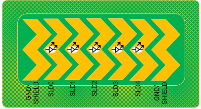
Sensor and device placement
Follow these guidelines while placing the sensor and the device in your PCB design:
Minimize the trace length from the device pins to the sensor pad
Mount series resistors within 10 mm of the device pins to reduce RF interference and provide ESD protection. See
Series resistors on CAPSENSE™ pins
for details
Mount the device and the other components on the bottom layer of the PCB
Avoid connectors between the sensor and the device pins because connectors increase C P and noise pickup
Button to Button distance (edge to edge) must be greater than 8 mm. If keys have less than 8 mm between them, there will be cross talk between the keys. Also, from a usability standpoint, it increases the risk of the user touching two keys at the same time. Key to key distance must be greater than 8 mm
Spacing from a touch line to any metal should be greater than 5 mm. This includes the metal chassis, decorative chrome trim, screws, and so on
Isolate or provide physical separation between CAPSENSE™ components and their signals from noisy subsystems such as transformers. A CAPSENSE™ system in general is sensitive to external noise
Trace length and width
Use short and narrow PCB traces to minimize the parasitic capacitance of the sensor. The maximum recommended trace length is 12 inches (300 mm) for a standard PCB and 2 inches (50 mm) for flex circuits. The maximum recommended trace width is 7 mil (0.18 mm). You should surround the CAPSENSE™ traces with a hatched ground or hatched shield with trace-to-hatch clearance of 10 mil to 20 mil (0.25 mm to 0.51 mm).
Trace routing
You should route the sensor traces on the bottom layer of the PCB, so that the finger does not interact with the traces. Do not route traces directly under any sensor pad unless the trace is connected to that sensor.
Do not run capacitive sensing traces closer than 0.25 mm to switching signals or communication lines. Increasing the distance between the sensing traces and other signals increases the noise immunity. If it is necessary to cross communication lines with sensor pins, make sure that the intersection is at right angles, as
Figure 226
shows.
Figure 226. Routing of sensor and communication lines
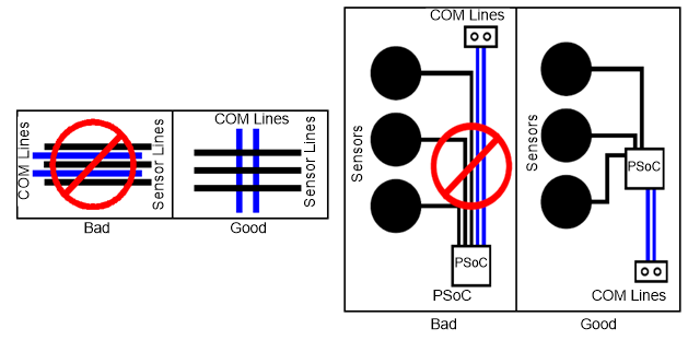
If, due to spacing constraints, sensor traces run in parallel with high-speed traces such as I
2
C communication lines or Bluetooth® LE antenna traces, it is recommended to place a ground trace between the sensor trace and the high-speed trace as shown in
Figure 227
. This guideline also applies to the cross talk caused by CAPSENSE™ sensor trace with precision analog trace such as traces from temperature sensor to the PSOC™ device. The thickness of the ground trace can be 7 mils and the spacing from sensor trace to ground trace should be equal to minimum of 10 mils to reduce the C
P
of the CAPSENSE™ sensor.
Figure 227. Reducing cross talk between high-speed switching trace and CAPSENSE™ trace
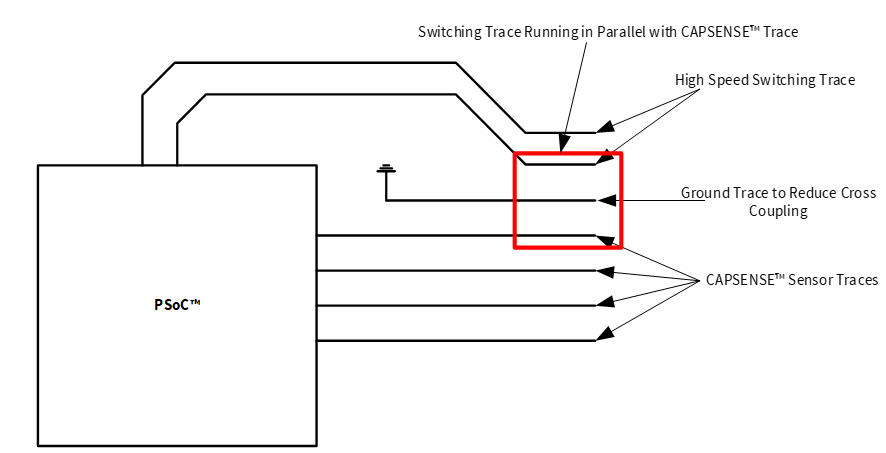
If a ground trace cannot be placed in between the switching trace and the CAPSENSE™ trace, the 3W rule can be followed to reduce the cross talk between the traces. The 3W rule states that “to reduce cross talk from adjacent traces, a minimum spacing of two trace widths should be maintained from edge to edge” as shown in
Figure 228
.
Figure 228. 3W trace spacing to minimize cross talk

Do not run Tx and Rx lines parallel to each other. The trace routing should be separated as much as possible
If the layout constraints require Tx and Rx run parallel for short distances, the space between Tx and Rx should be greater than the distance between Tx and Rx inside the key (2 times the Tx-Rx key spacing is preferred) or add ground between them
Keep as much clearance around Rx as possible to prevent noise on the touch keys. It is critical to follow this guideline for spacing to power traces and LED lines (high speed switching, power). Ground should also follow this rule, but it is less critical. Ground will provide noise protection but will reduce key sensitivity
For a given set of sensors, the number of Rx lines must be less than or equal to Tx lines. Rx lines are susceptible to noise, whereas Tx lines are relatively less susceptible
Crosstalk solutions
A common backlighting technique for panels is an LED mounted under the sensor pad so that it is visible through a hole in the middle of the sensor pad. When the LED is switched ON or OFF, voltage transitions on the LED trace can create crosstalk in the capacitive sensor input, creating noisy sensor data. To prevent this crosstalk, isolate CAPSENSE™ and the LED traces from one another as
Trace routing
section explains.
You can also reduce crosstalk by removing the rapid transitions in the LED drive voltage, by using a filter as
Figure 229
shows. Design the filter based on the required LED response speed.
Figure 229. Reducing crosstalk
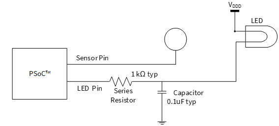
A guard trace is a ground trace running close to or above/below a TX/Rx line of a mutual-capacitance button. Guard traces can be used to protect sensor traces from noise if the layout does not allow for a ground hatch. Similar to ground hatch, guard traces add parasitic capacitance and reduce button sensitivity. Guard traces are usually needed on a case-by-case basis. Typical situations where guard traces have been used in the past include:
Reduce cross talk
Protect from noise of high-speed lines (I2C, SPI, UART) and toggling LED traces
Border around the HMI or around an LCD
Vias
Use the minimum number of vias possible to route CAPSENSE™ signals, to minimize parasitic capacitance. Place the vias on the edge of the sensor pad to reduce trace length, as
Figure 230
shows.
Figure 230. Via placement on the sensor pad
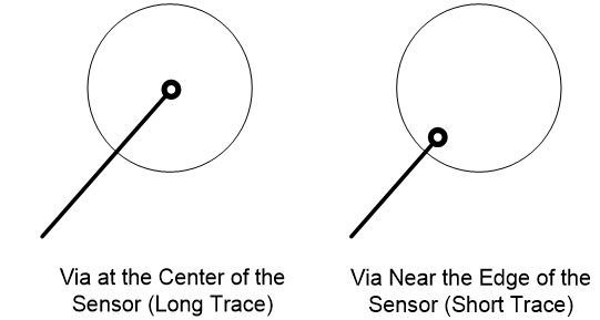
Ground plane
When designing the ground plane, follow these guidelines:
Ground surrounding the sensors should be in a hatch pattern. If you are using ground or driven-shield planes in both top and bottom layers of the PCB, you should use a 25 percent hatching on the top layer (7-mil line, 45-mil spacing), and 17 percent on the bottom layer (7 mil line, 70 mil spacing)
For the other parts of the board not related to CAPSENSE™, solid ground should be present as much as possible
The ground planes on different layers should be stitched together as much as possible, depending on the PCB manufacturing costs. Higher amount of stitching results in lower ground inductance, and brings the chip ground closer to the supply ground. This is important especially when there is high current sinking through the ground, such as when the radio is operational
Every ground plane used for CAPSENSE™ should be star-connected to a central point, and this central point should be the sole return path to the supply ground. Specifically:
The hatch ground for all sensors must terminate at the central point
The ground plane for C MOD , CINTX must terminate at the central point
The ground plane for CSH_TANK must terminate at the central point
explains the star connection. The central point for different families is mentioned in
Table 37
.
Figure 231. Star connection for Ground

Family | Central point |
|---|---|
PSOC™ 4000 | VSS pin |
PSOC™ 4100/4100M | VSS pin |
PSOC™ 4200/4200M/4200L/PSOC™ 4-S/PSOC™ 4100PS | VSS pin |
PSOC™ 4100-BL | E-pad |
PSOC™ 4200-BL | E-pad |
All the ground planes for CAPSENSE™ should have an inductance of less than 0.2 nH from the central point. To achieve this, place the C MOD , CINTx , and CSH_TANK capacitor pads close to the chip, and keep their ground planes thick enough
Using packages without E-pad
When not using the E-pad, the VSS pin should be the central point and the sole return path to the supply ground. High-level layout diagrams of the top and bottom layers of a board when using a chip without the E-pad are shown in
Figure 232
and
Figure 233
.
Figure 232. PCB top layer layout using a chip without E-pad
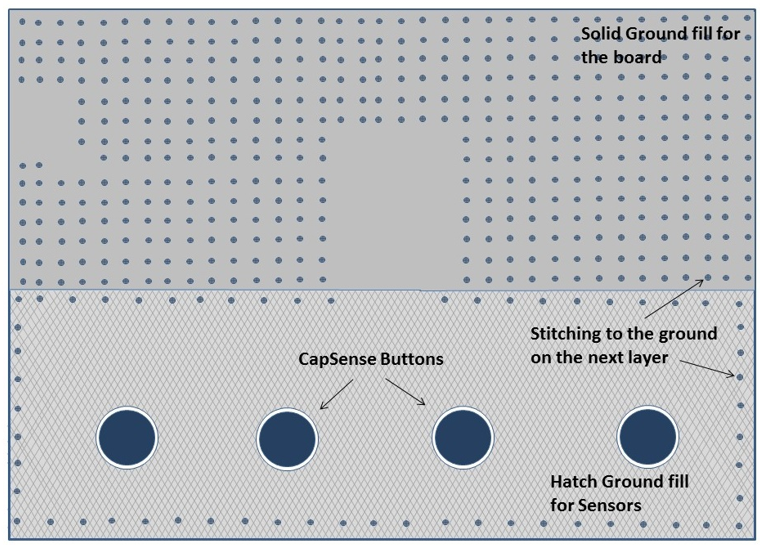
Figure 233. PCB bottom layer layout using a chip without E-pad
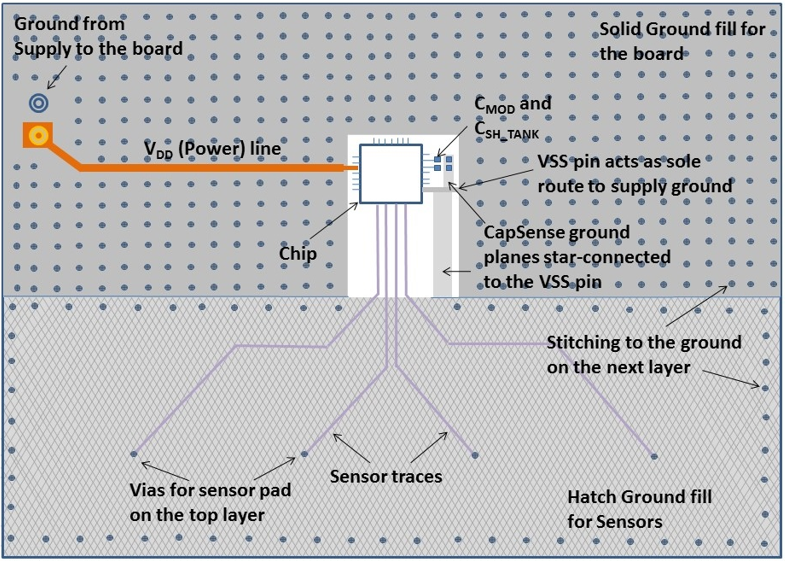
Using packages with E-pad
If you are using packages with E-pad, the following guidelines must be followed:
The E-pad must be the central point and the sole return path to the supply ground
The E-pad must have vias underneath to connect to the next layers for additional grounding. Generally unfilled vias are used in a design for cost purposes, but silver-epoxy filled vias are recommended for the best performance as they result in the lowest inductance in the ground path
Using PSOC™ 4 Bluetooth® LE devices
In the case of PSOC™ 4 Bluetooth® LE devices in the QFN package (with E-pad):
The general guidelines of ground plane (discussed above) apply
The E-pad usage guidelines of Using packages with E-pad apply
The VSSA pin should be connected to the E-pad below the chip itself
The vias underneath the E-pad are recommended to be 5x5 vias of 10-mil size
High-level layout diagrams of the top and bottom layers of a board when using PSOC™ 4 Bluetooth® LE chips are shown in
Figure 234
and
Figure 235
.
Figure 234. PCB top layer layout with PSOC™ 4Bluetooth® LE (with E-pad)
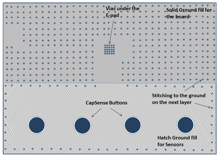
Figure 235. PCB bottom layer layout with PSOC™ 4 Bluetooth® LE (with E-pad)
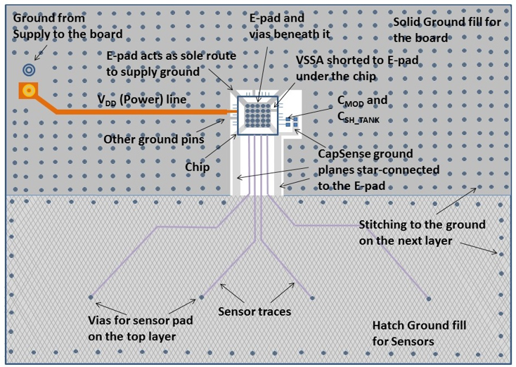
Power supply layout recommendations
CAPSENSE™ is a high-sensitivity analog system. Therefore, a poor PCB layout introduces noise in high-sensitivity sensor configurations such as proximity sensors and buttons with thick overlays (>1 mm). To achieve low noise in a high-sensitivity CAPSENSE™ design, the PCB layout should have decoupling capacitors on the power lines, as listed in
Table 38
.
Power line | Decoupling capacitors | Corresponding ground terminal | Applicable device family |
|---|---|---|---|
VDD | 0.1 µF and 1 µF | VSS | PSOC™ 4000 |
VDDIO | 0.1 µF and 1 µF | VSS | PSOC™ 4000, PSOC™ 6 MCU |
VDDD | 0.1 µF and 1 µF | VSS | PSOC™ 4100, PSOC™ 4200, PSOC™ 6 MCU |
0.1 µF and 1 µF | VSSD | PSOC™ 4100-BL, PSOC™ 4200-BL, PSOC™ 4200L, PSOC™ S-series, PSOC™ 4100S Plus, PSOC™ 4100S Max | |
See device datasheet | VSSD | PSOC™ 4000T, PSOC™ 4100T Plus | |
VDDA 17 | 0.1 µF and 1 µF (Battery powered supply) | VSSA | PSOC™ 4100, PSOC™ 4200, PSOC™ 4100-BL, PSOC™ 4200-BL, PSOC™ 4200L, PSOC™ 4S-Series, PSOC™ 4100S Plus, PSOC™ 4100PS, PSOC™ 6 MCU |
0.1 µF and 10 µF (Mains Powered supply) | VSSA | PSOC™ 4S-series, PSOC™ 4100S Plus, PSOC™ 4100PS | |
VDDR | 0.1 µF and 1 µF | VSSD | PSOC™ 4100-BL, PSOC™ 4200-BL, PSOC™ 6 MCU with Bluetooth® LE Connectivity |
VCCD | See device datasheet | VSS (PSOC™ 4000) or VSSD (all others) | All device families |
The decoupling capacitors and
C
MOD
capacitor must be placed as close to the chip as possible to keep ground impedance and supply trace length as low as possible.
For further details on bypass capacitors, see the Power section in the
Device datasheet
.
Layout guidelines for liquid tolerance
As explained in the
Liquid tolerance
section, by implementing a shield electrode and a guard sensor, a liquid-tolerant ™ system can be implemented. If there are multiple CSD blocks in the device, each CSD block should have a dedicated shield electrode. This section shows how to implement a shield electrode and a guard sensor.
Layout guidelines for shield electrode
The area of the shield electrode depends on the size of the liquid droplet and the area available on the board for implementing the shield electrode. The shield electrode should surround the sensor pads and traces, and spread no further than 1 cm from these features. Spreading the shield electrode beyond 1 cm has negligible effect on system performance.
Also, having a large shield electrode may increase radiated emissions. If the board area is very large, the area outside the 1-cm shield electrode should be left empty, as
Figure 236
shows. The board design should focus on reducing the coupling capacitance between the liquid droplet and ground. Thus, for improved liquid tolerance, there should not be any hatch fill or a trace connected to ground in the top and bottom layers of the PCB.
When there is a grounded hatch fill or a trace then, when a liquid droplet falls on the touch surface, it may cause sensor false triggers. Even if there is a shield electrode between the sensor and ground, the effect of the shield electrode will be totally masked out and sensors may false trigger.
In some applications, there may not be sufficient area available on the PCB for shield electrode implementation. In such cases, the shield electrode can spread less than 1 cm; the minimum area for shield electrode can be the area remaining on the board after implementing the sensor.
In some applications, the capacitance of the shield electrode will be very high; you can reduce it with the following techniques:
Using multiple shield electrode instead of single shield electrode: If there is a single hatch pattern with a higher CP , split the hatch pattern into multiple hatch patterns and drive it with the shield signal to decrease the shield C P . This will also allow the use of a higher range of sense clock frequencies for the sensors which will improve the sensitivity of the CAPSENSE™ system. In a complex layout design, this approach will make trace routing simple
Connecting multiple shield pins to the same electrode: If splitting the shield electrode in the layout is not feasible, connect multiple shield pins to the same electrode. This will make all the series resistance of the sensor pins in parallel and reduce the effective time constant of the shield electrode, which will allow using a higher range of sense clock frequencies for sensors, which will improve the sensitivity of the CAPSENSE™ system
Figure 236. Shield electrode placement when sensor trace Is routed in top and bottom layer
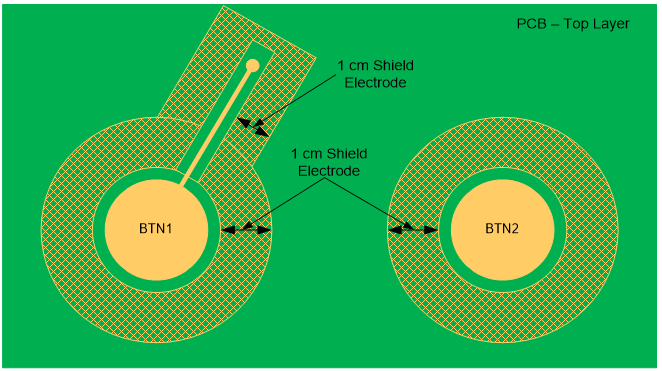
Follow these guidelines to implement the shield electrode in two-layer and four-layer PCBs:
Two-layer PCB:
Top layer: Hatch fill with 7 mil trace and 45 mil grid (25 percent fill). Hatch fill should be connected to the driven-shield signal
Bottom layer: Hatch fill with 7 mil trace and 70 mil grid (17 percent fill). Hatch fill should be connected to the driven-shield signal
Four (or more)-layer PCB:
Top layer: Hatch fill with 7 mil trace and 45 mil grid (25 percent fill). Hatch fill should be connected to the driven-shield signal
Layer-2: Hatch fill with 7 mil trace and 70 mil grid (17 percent fill). Hatch fill should be connected to the driven-shield signal
Layer-3: VDD Plane
Bottom layer: Hatch fill with 7 mil trace and 70 mil grid (17 percent fill). Hatch fill should be connected to ground
The recommended air gap between the sensor and the shield electrode is 1 mm.
Layout guidelines for guard sensor
As explained in the
Guard sensor
section, the guard sensor is a copper trace that surrounds all sensors, as
Figure 237
shows.
Figure 237. PCB layout with shield electrode and guard sensor
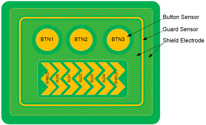
The guard sensor should be triggered only when there is a liquid stream on the touch surface. Ensure that the shield electrode pattern surrounds the guard sensor to prevent it from turning on due to liquid droplets. The guard sensor should be placed such that it meets the following conditions:
It should be the first sensor to turn on when there is a liquid stream on the touch surface. To accomplish this, the guard sensor is usually placed such that it surrounds all sensors
It should not be accidentally touched while pressing a button or slider sensor. Otherwise, the button sensors and slider sensor scanning will be disabled and the CAPSENSE™ system will become nonoperational until the guard sensor is turned off. To ensure the guard sensor is not accidentally triggered, place the guard sensor at a distance greater than 1 cm from the sensors
Follow these guidelines to implement the guard sensor:
The guard sensor should be in the shape of a rectangle with curved edges and should surround all the sensors
The recommended thickness for a guard sensor is 2 mm
The recommended clearance between the guard sensor and the shield electrode is 1 mm
If there is no space on the PCB for implementing a guard sensor, the guard sensor functionality can be implemented in the firmware. For example, you can use the ON/OFF status of different sensors to detect a liquid stream depending on the use case data.
The following conditions can be used to detect a liquid stream on the touch surface:
When there is a liquid stream, more than one button sensor will be active at a time. If your design does not require multi-touch sensing, you can detect this and reject the sensor status of all the button sensors to prevent false triggering
In a slider, if the slider segments which are turned ON are not adjacent segments, you can reset the slider segments status or reject the slider centroid value that is calculated
A firmware algorithm to detect the false touch due to water drop from the use case data can be made to improve the false touch rejection capability sensors
Liquid tolerance with ground ring
In some applications, it is required to have a ground ring (solid trace or a hatch fill) around the periphery of the board for improved ESD performance, as shown in
Figure 238
. The ground ring is used to redirect the ESD as explained in
Redirect
. Having a ground ring around the board may result in sensor false triggers when liquid droplets fall in between the sensor and the ground sensor. Therefore, it is recommended not to have any ground in the top layer. If the design must have a ground ring in the top layer, use a ground ring with the minimum thickness (8 mils).
Figure 238. CAPSENSE™ design with ground ring for improved ESD performance

Schematic rule checklist
provides the checklist to verify your CAPSENSE™ schematic.
No. | Category | Recommendations/Remarks |
|---|---|---|
1 | CMOD | 2.2 nF. X7R or NP0 capacitors can be used for C MOD . X7R type C MOD will experience very large raw count variation and probably saturation in applications where the temperature range is well above ambient (that is, > 50C). Hence, it is recommended to select the C MOD capacitor type according to the expected operating temperature range. See Table 40 for pin selection. |
2 | C SH_TANK 18 | 10 nF if shield electrode is used; NA otherwise. See Driven shield signal and shield electrode and CAPSENSE™ CSD shielding for details on shield electrode and use of C SH_TANK respectively. See Table 40 for pin selection. |
3 | CINTA / CINTB 19 | 470 pF. See Table 40 for pin selection. |
4 | Series resistance on input lines | 560 Ω for self-capacitance and 2 kΩ for mutual-capacitance. See Series resistors on CAPSENSE™ pins ford etails. |
5 | Sensor pin selection | If possible, avoid pins that are close to the GPIOs carrying switching/communication signals. Physically separate DC loads such as LEDs and I 2 C pins from the CAPSENSE™ pins by a full port wherever possible. See Sensor pin selection section for more details. |
6 | GPIO source/sink current | Ensure that the total sink current through GPIOs is not greater than 40 mA when the CAPSENSE™ block is scanning the sensors. |
7 | Series resistance on shield lines | 560 Ω recommended on shield lines. |
8 | Recommended CAPSENSE™ PORT | PSOC™ 4100T Plus, the recommended ports are 0, 1, 3, 4, 5, 6. PSOC™ 4100S Max, the recommended ports are : Channel 0: 3, 4, 6,10, 11, 12 and Channel 1: 0, 5, 7, 8, 9. See AMUX Splitter switch noise for more details. |
External capacitors pin selection
As explained in the CAPSENSE™ fundamentals section, CAPSENSE™ requires the following external capacitors for reliable operation - CMOD (capacitive sigma-delta (CSD) sensing method), CTANK (only when Shield is implemented), and C INTX (CSX sensing method). Starting from PSOC™ Creator 3.3 SP2 , the number of pins that can support CMOD and CSH_TANK is increased to improve design flexibility. Table 40 lists the recommended pins for CMOD , C INTX , and CSH_TANK capacitors for PSOC™ Creator 3.3 SP2 or later versions.
Note: For PSOC™ 4100/PSOC™ 4200, if you select a pin other than P4[2] forCMOD, P4[2] will not be available for any other function. For example, if you try routingCMODto P2[0] in PSOC™ Creator for a PSOC™ 4200 device, it uses both P2[0] and P4[2].
Device | C MOD (or C MOD1 for fifth-generation CAPSENSE™) | CSH_TANK (or CMOD2 for fifth-generation CAPSENSE™) |
|---|---|---|
PSOC™ 4000 | P0[4] | P0[2] |
PSOC™ 4100/PSOC™ 4200 | P4[2] | P4[3] |
PSOC™ 4200M/PSOC™� 4200L | CSD0: P4[2] | CSD0: P4[3] |
CSD1: P5[0] | CSD1: P5[1] | |
PSOC™ 4 Bluetooth® LE | P4[0] | P4[1] |
PSOC™ 6 MCU | P7[1] | P7[2] |
PSOC™ 4S-Series, PSOC™ 4100S Plus | P4[2] | P4[3] |
PSOC™ 4100PS | P5[2] | P5[3] |
PSOC™ 4100S Max | Channel0: P4[0] | Channel0: P4[1] |
Channel1: P7[0] | Channel1: P7[1] | |
PSOC™ 4000T | P4[2] | P4[3] |
PSOC™ 4100T Plus | P1[0] | P1[1] |
Device | CMOD (or CMOD1 for fifth-generation CAPSENSE™) | CSH_TANK (or CMOD2 for fifth-generation CAPSENSE™) | CINTA | CINT B |
|---|---|---|---|---|
PSOC™ 4000 | Port0[0:7], Port1 [0:7]P2[0] | Port0 [0:7], Port1 [0:7]P2[0] | P0[4] | P0[2] |
PSOC™ 4100 | Port0 [0:7], Port1 [0:7]Port2 [0:7], Port3 [0:7]P4[2] | Port0 [0:7], Port1 [0:7]Port2 [0:7], Port3 [0:7]P4[3] | Not supported | Not supported |
PSOC™ 4200 | Port0 [0:7], Port1 [0:7]Port2 [0:7], Port3 [0:7]P4[2] | Port0 [0:7], Port1 [0:7], Port2 [0:7], Port3 [0:7]P4[3] | Port0 [0:7], Port1 [0:7]Port2 [0:7], Port3 [0:7] | Port0 [0:7], Port1 [0:7]Port2 [0:7], Port3 [0:7] |
PSOC™ 4200M | CSD0: Port0 [0:7], Port1 [0:7] Port2 [0:7], Port3 [0:7] Port4 [0:6], Port6 [0:5] Port7 [0:1] | CSD0: Port0 [0:7], Port1 [0:7]Port2 [0:7], Port3 [0:7], Port4 [0:6], Port6 [0:5] Port7 [0:1] | CSD0: P4[2] | CSD0: P4[3] |
CSD1: Not supported | CSD1: Not supported | CSD1: Not supported | CSD1: Not supported | |
PSOC™ 4200L | CSD0: Port0 [0:7], Port1 [0:7] Port2 [0:7], Port3 [0:7] Port4 [0:6], Port6 [0:5] Port7 [0:7], Port10 [0:7], Port11 [0:7] | CSD0: Port0 [0:7], Port1 [0:7] Port2 [0:7], Port3 [0:7] Port4 [0:6], Port6 [0:5] Port7 [0:7], Port10 [0:7] Port11 [0:7] | CSD0: P4[2] | CSD0: P4[3] |
CSD1: Port5 [0:7], Port8 [0:7] Port9 [0:7] | CSD1: Port5 [0:7], Port8 [0:7] Port9 [0:7] | CSD1: P5[0] | CSD1: P5[1] | |
PSOC™ 4 Bluetooth® LE | Port0 [0:7], Port1 [0:7]Port2 [0:7], Port3 [0:7]Port4 [0:1], Port5 [0:1]Port6 [0:1] | Port0 [0:7], Port1 [0:7]Port2 [0:7], Port3 [0:7]Port4 [0:1], Port5 [0:1]Port6 [0:1] | P4[0] | P4[1] |
PSOC™ 6 MCU | P7[1] or P7[2] or P7[7] | P7[1] or P7[2] or P7[7] | P7[1] | P7[2] |
PSOC™ 4S-Series, PSOC™ 4100S Plus | P4[2], P4[3], P4[1] | P4[2], P4[3], P4[1] | P4[2] | P4[3] |
PSOC™ 4100PS | P5[0], P5[2], P5[3] | P5[0], P5[2], P5[3] | P5[2] | P5[3] |
PSOC™ 4100S Max 20 | Channel0: P4[0], P4[2] | Channel0: P4[1], P4[3] | Not applicable | Not applicable |
Channel1: P7[0], P5[1] | Channel1: P7[1], P5[2] | |||
PSOC™ 4000T | P4[2] | P4[3] | Not applicable | Not applicable |
PSOC™ 4100T Plus | P1[0] | P1[1] | Not applicable | Not applicable |
Sensor pin selection
As explained in CAPSENSE™ fundamentals , PSOC™ supports CSD and CSX capacitive sensing methods. Each CSD sensor requires a single sensor pin and CSX sensor will require two sensor pins for Tx and Rx electrode in addition to the required external capacitors for each sensing technique.
The selection of the sensor pins should be in a way such that the CAPSENSE™ sensor traces and communication or other toggling GPIO traces are isolated by proper port/pin assignment. The following are some recommended guidelines:
Isolate switching signals, such as PWM, I2C communication lines, and LEDs from the sensor and sensor traces. Place them at least 4 mm apart and fill a hatched ground between the CAPSENSE™ traces and the switching signals to avoid crosstalk
Distribute the placement of DC loads on different ports to reduce the noise in CAPSENSE™. It is recommended to have digital I/Os spread on different ports rather than concentrating in a single port
While the CAPSENSE™ block is scanning the sensor, limit the total source or sink current through GPIOs to less than 40 mA while the CAPSENSE™ block is scanning the sensor. Sinking a current greater than 40 mA while the CAPSENSE™ sensor is scanning may result in excessive noise in the sensor raw count
For a PSOC™ 4 device it is recommended to place all the digital DC loads like LEDs, I2C/UART communication pins on the port powered by only VSSD; see the Device datasheet for determining the ports that are powered by VSSD. Placing DC loads on ports powered by VSSA will shift the VSSA up. Since CAPSENSE™ is powered by VSSA, it will affect its performance
For PSOC™ 6 family of devices:
Table 42 lists the ports that support CAPSENSE™, selecting ports 5, 6, 7, and 8 for CAPSENSE™ ensures lesser noise
It is recommended to place all digital switching pins such as LEDs, I 2 C, UART, SPI, SMIF communication pins on the ports that are powered by a different power supply domain which is not shared with the CAPSENSE™ ports. Table 43 lists the ports, their supply domains, and recommendations for using these ports with CAPSENSE™. For more details, see the Errata section of the Device datasheet . A deviation from these guidelines might cause a noise due to level shift in raw count. For more details, see Raw counts show a level-shift or increased noise when GPIOs are toggled . To isolate the supply domains further, it is better to externally isolate them using ferrite beads as shown in Figure 240
Device | CAPSENSE™ capable ports |
|---|---|
CY8C62x6, CY8C62x7 | P0, P1, P2, P4, P5, P6, P7, P8, P9, P10, P11 |
CY8C63x6, CY8C63x7 | P0, P1, P2, P4, P5, P6, P7, P8, P9, P10, P11 |
CY8C62x5 | P7.0 to P7.7, P8.0 to P8.3, P9.0 to P9.3 |
Ports | Supply domain | Recommended for CAPSENSE™ | Recommendations for GPIOs if used for communication, LEDs, and other high frequency functionality with CAPSENSE™ |
|---|---|---|---|
P0 | VBACKUP | No* | Switching frequency < 8 MHz |
P1 | VDDD | No* | Switching frequency < 1 MHz, SLOW Slew Rate |
P2, P3, P4 | VDDIO2 | No* | Switching frequency < 25 MHz |
P5, P6, P7, P8 | VDDIO1 | Yes | Not recommended |
P9, P10 | VDDIOA | No* | Switching frequency < 1 MHz, SLOW Slew Rate |
P11, P12, P13 | VDDIO0 | No* | Switching frequency < 80 MHz |
P14 | VDDUSB | No* | NA |
Note: * If you need additional CAPSENSE™ pins and if you must use GPIOs in ports P1, P9, and P10 as Tx electrode for CSX sensor, restrict the Tx clock frequency within 1 MHz and use SLOW slew rate.Figure 239shows an example on how to select theSlew Rateof the GPIO using theDevice configuratorin the ModusToolbox™ project. Note that using the ports other than the recommended ports for CAPSENSE™ might cause higher noise in raw count.
Figure 239. Selecting slew rate for GPIOs
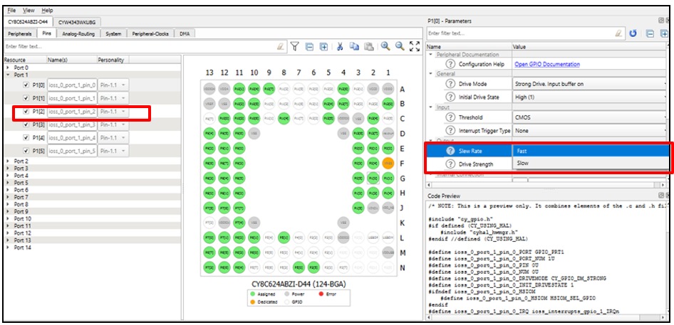
Figure 240. Externally isolated supply domains
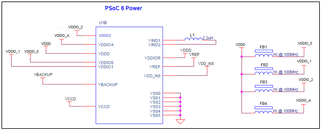
Layout rule checklist
Table 44 provides the checklist to help verify your layout design.
No. | Category | Minimum value | Maximum value | Recommendations/Remarks | |
|---|---|---|---|---|---|
1 | Button | Shape | N/A | N/A | Circle or rectangular with curved edges |
Size | 5 mm | 15 mm | 10 mm | ||
Clearance to ground hatch | 0.5 mm | 2 mm | Should be equal to overlay thickness | ||
2 | Slider | Width of segment | 1.5 mm | 8 mm | 8 mm |
Clearance between segments | 0.5 mm | 2 mm | 0.5 mm | ||
Height of segment | 7 mm | 15 mm | 12 mm | ||
3 | Overlay | Type | N/A | N/A | Material with high relative permittivity (except conductors) Remove any air gap between sensor board and overlay/front panel of the casing. |
Thickness for buttons | N/A | 5 mm | |||
Thickness for sliders | N/A | 5 mm | |||
Thickness for touchpads | N/A | 0.5 mm | |||
4 | Sensor traces | Width | N/A | 7 mil | Use the minimum width possible with the PCB technology that you use. |
Length | N/A | 300 mm for a standard (FR4) PCB 50 mm for flex PCB | Keep as low as possible. | ||
Clearance to ground and other traces | 0.25 mm | N/A | Use maximum clearance while keeping the trace length as low as possible. | ||
Routing | N/A | N/A | Route on the opposite side of the sensor layer. Isolate from other traces. If any non-CAPSENSE™ trace crosses the CAPSENSE™ trace, ensure that intersection is orthogonal. Do not use sharp turns. | ||
5 | Via | Number of vias | 1 | 2 | At least one via is required to route the traces on the opposite side of the sensor layer. |
Hole size | N/A | N/A | 10 mil | ||
6 | Ground | Hatch fill percentage | N/A | N/A | Use hatch ground to reduce parasitic capacitance. Typical hatching: 25% on the top layer (7 mil line, 45 mil spacing) 17% on the bottom layer (7 mil line, 70 mil spacing) |
7 | Series resistor | Placement | N/A | N/A | Place the resistor within 10 mm of the PSOC™ pin. See Figure 241 for an example placement of series resistance on board. |
8 | Shield electrode | Spread | N/A | 1 cm | If you have PCB space, use 1-cm spread. |
9 | Guard sensor (for water tolerance) | Shape | N/A | N/A | Rectangle with curved edges |
Thickness | N/A | N/A | Recommended thickness of guard trace is 2 mm and distance of guard trace to shield electrode is 1 mm. | ||
10 | Ground Ring(for ESD protection) | Shape | N/A | N/A | Around the board periphery with curved edges. Can be a solid trace or a hatch fill. |
Thickness | N/A | N/A | Not recommended in top layer as it can cause sensor false triggers with liquid droplets. If design must have a Ground Ring in the top layer, use a minimum thickness ring of 8 mils. | ||
11 | CMOD | Placement | N/A | N/A | Place close to the PSOC™ pin. See Figure 241 for an example placement of CMOD on PCB. |
12 | CSH_TANK | Placement | N/A | N/A | Place close to the PSOC™ pin. See Figure 241 for an example placement of CSH_TANK on board. |
13 | C INTA | Placement | N/A | N/A | Place close to the PSOC™ pin. See Figure 241 for an example placement of CINTA on the PCB. |
14 | CINTB | Placement | N/A | N/A | Place close to the PSOC™ pin. See Figure 241 for an example placement of INTA on the PCB. |
Figure 241. Example placement for CMOD , C INTx , C SH_TANK , and series resistance on input lines in the PSOC™ 4200M device
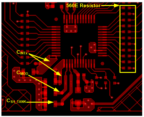
Noise in CAPSENSE™ system
Finger injected noise
If the power supply design of the system is poor, the power and ground supplies of a device fluctuates in voltage relative to the finger ground (earth ground) in a common mode fashion. This type of noise is called common mode noise.
Figure 242
illustrates the common mode noise, where both the 5 V and the 0 V output leads of the power supply remain 5 V from each other, but they move up and down together, in a “common mode” manner.
This is not a problem, until a finger touch occurs on the button. A finger touch on the button introduces a (capacitive) path to the same earth ground and it will create a path for charge flow, which is equivalent to a noise signal injected exactly at the finger touch location. This injected noise caused by the common mode noise in power supply is called finger injected noise. It is observed only during the finger touch on the button in AC powered application and it doesn’t occur in battery powered application.
Figure 242. Common mode noise in the power supply
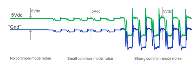
Note: When the complete system powered by AC supply is held in hand of the user, the entire system will be grounded to earth sufficiently and no significant “common-mode” noise would flow through the touching finger to earth. However, if the system is connected to the power supply and placed on a desk, a touch on the button, can introduce a problematic discharge path to ground.
Recommendations to reduce the finger injected noise
The finger injected noise could be reduced by properly following the layout and schematics guidelines described in this section. The general recommendations to reduce the finger injected noise is explained below.
Fill the PCB board around the button with hatched pattern and connected it to device ground. Follow the recommendations as mentioned in the section Ground plane.
shows the impact of ground on the finger injected noise for mutual capacitance button and it is also true for CSD sensing technique. In the left figure, the system doesn’t have the hatched ground around the button and most of the injected noise through the finger pass to the Rx pin of the device through the Capacitance formed between the finger and Rx electrode. In the right figure, the system has the hatched ground around the button and thus the finger injected noise is having an alternate path to flow which results in the reduction of the noise reaching to the device Rx pin.
Figure 243. Effect of ground on finger injected noise
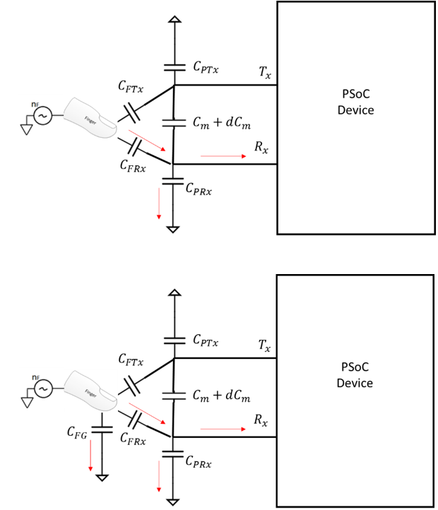
Better power supply design of the system could easily eliminate the common mode noise, which will in turn reduce the finger injected noise
Use software technique that are available in the CAPSENSE™ component to combat the finger injected noise such as selecting optimal sensing clock frequency and Multi frequency scanning, and so on
Increase the overlay thickness will reduce the finger injected noise as it will decrease the capacitance formed between the finger and Rx electrode
VDDA noise
The noise in the system due to unwanted voltage ripples in the VDD supply is called VDDA noise.
Recommendations to reduce the VDDA noise
The VDDA noise could be reduced by properly following the layout and schematics guidelines in this chapter. The general recommendations to reduce the VDDA noise as follows:
Use clean power supply and have VDD ripples below the limits mentioned in the device datasheet
Use filters or an LDO regulator on the VDD power lines. Fifth-gen and fifth-gen low-power CAPSENSE™ devices are more robust towards power supply ripple compared to previous-generation CAPSENSE™ devices. The user may not need any LDO to design with these devices if the power supply ripple is within the limits mentioned in the datasheet. However, the user is advised to validate and ensure that overall system-level performance requirements are met
Use decoupling capacitors on the power supply pins to reduce the conducted noise from the power supply
To reduce high-frequency noise, place a ferrite bead around power supply or communication lines
Selecting the proper supply configuration as mentioned in the Power section in the Device datasheet and using the internal regulator to the device might help in reducing the VDDA noise
External noise
Any noise that is injected into to the system through the routing trace lines like ESD, EMI, conducted noise are coming into the category of external noise. The recommended guidelines for reducing the impact of the external noise are discussed in this section.
ESD protection
The nonconductive overlay material used in CAPSENSE™ provides inherent protection against ESD.
Table 45
lists the thickness of various overlay materials, required to protect the CAPSENSE™ sensors from a 12 kV discharge (according to the IEC 61000 4 2 specification).
Material | Breakdown voltage (V/mm) | Minimum overlay thickness for protection against 12 kV ESD (mm) |
|---|---|---|
Air | 1200 – 2800 | 10 |
Wood – dry | 3900 | 3 |
Glass – common | 7900 | 1.5 |
Glass – Borosilicate (Pyrex®) | 13,000 | 0.9 |
PMMA Plastic (Plexiglas®) | 13,000 | 0.9 |
ABS | 16,000 | 0.8 |
Polycarbonate (Lexan®) | 16,000 | 0.8 |
Formica | 18,000 | 0.7 |
FR-4 | 28,000 | 0.4 |
PET Film (Mylar®) | 280,000 | 0.04 |
Polyimide Film (Kapton®) | 290,000 | 0.04 |
If the overlay material does not provide sufficient protection (for example, ESD from other directions), you can apply other ESD counter-measures, in the following order:
Prevent
,
Redirect
, and
ESD protection devices
.
Preventing ESD discharge
Preventing the ESD discharge from reaching the PSOC™ is the best countermeasure you can take. Make sure that all paths to PSOC™ have a breakdown voltage greater than the maximum ESD voltage possible at the surface of the equipment. You should also maintain an appropriate distance between the PSOC™ and possible ESD sources. In the example illustrated in
Figure 244
, if L1 and L2 are greater than 10 mm, the system can withstand a 12 kV ESD.
Figure 244. ESD paths
If it is not possible to maintain adequate distance, place a protective layer of nonconductive material with a high breakdown voltage between the possible ESD source and PSOC™. One layer of 5 mil thick Kapton® tape can withstand 18 kV. See
Table 45
for other material dielectric strengths.
Redirect
If your product is densely packed, preventing the discharge event may not be possible. In such cases, you can protect the PSOC™ from ESD by redirecting the ESD. A standard practice is to place a ground ring on the perimeter of the circuit board, as
Figure 245
shows. The ground ring should connect to the chassis ground. Using a hatched ground plane around the button or slider sensor can also redirect the ESD event away from the sensor and PSOC™.
Figure 245. Ground ring

ESD protection devices
You can use ESD protection devices on vulnerable traces. Select ESD protection devices with a low input capacitance to avoid reduction in CAPSENSE™ sensitivity.
Table 46
lists the recommended ESD protection devices.
ESD protection device | Input capacitance | Leakage current | Contact maximum ESD limit | Air discharge maximum ESD limit | |
|---|---|---|---|---|---|
Manufacturer | Part number | ||||
Littelfuse | SP723 | 5 pF | 2 nA | 8 kV | 15 kV |
Vishay | VBUS05L1-DD1 | 0.3 pF | 0.1 µA | ±15 kV | ±16 kV |
NXP | NUP1301 | 0.75 pF | 30 nA | 8 kV | 15 kV |
Electromagnetic compatibility (EMC) considerations
EMC is related to the generation, transmission, and reception of electromagnetic energy that can affect the working of an electronic system. Electronic devices are required to comply with specific limits for emitted energy and susceptibility to external events. Several regulatory bodies worldwide set regional regulations to help ensure that electronic devices do not interfere with each other.
CMOS analog and digital circuits have very high input impedance. As a result, they are sensitive to external electric fields. Therefore, you should take adequate precautions to ensure their proper operation in the presence of radiated and conducted noise.
Computing devices are regulated in the US by the FCC under Part 15, Sub-Part B for unintentional radiators. The standards for Europe and the rest of the world are adapted from CENELEC. These are covered under CISPR standards (dual-labeled as ENxxxx standards) for emissions, and under IEC standards (also dual labeled as ENxxxx standards) for immunity and safety concerns.
The general emission specification is EN55022 for computing devices. This standard cover both radiated and conducted emissions. Medical devices in the US are not regulated by the FCC, but rather are regulated by FDA rules, which include requirements of EN55011, the European norm for medical devices. Devices that include motor controls are covered under EN55014 and lighting devices are covered under EN50015.
These specifications have essentially similar performance limitations for radiated and conducted emissions. Radiated and conducted immunity (susceptibility) performance requirements are specified by several sections of EN61000-4. Line voltage transients, ESD and some safety issues are also covered in this standard.
Radiated interference and emissions
While PSOC™ 4 and PRoC Bluetooth® LE offer a robust CAPSENSE™ performance, radiated electrical energy can influence system measurements and potentially influence the operation of the CAPSENSE™ processor core. Interference enters the CAPSENSE™ device at the PCB level through sensor traces and through other digital and analog inputs. CAPSENSE™ devices can also contribute to electromagnetic compatibility (EMC) issues in the form of radiated emissions.
Use the following techniques to minimize the radiated interference and emissions.
Hardware considerations
Ground Pane
In general, proper ground plane on the PCB reduces both RF emissions and interference. However, solid grounds near CAPSENSE™ sensors or traces connecting these sensors to PSOC™ pins increase the parasitic capacitance of the sensors. It is thus recommended to use hatched ground planes surrounding the sensor and on the bottom layer of the PCBs, below the sensors, as explained in the
Ground plane
section in
PCB layout guidelines
. Solid ground may be used below the device and other circuitry on the PCB which is farther from CAPSENSE™ sensors and traces. A solid ground flood is not recommended within 1 cm of CAPSENSE™ sensors or traces.
Series resistors on CAPSENSE™ pins
Every CAPSENSE™ controller pin has some parasitic capacitance (
C
P
) associated with it. As
Figure 246
shows, adding an external resistor forms a low-pass RC filter that attenuates the RF noise amplitude coupled to the pin. This resistance also forms a low-pass filter with the parasitic capacitance of the CAPSENSE™ sensor that significantly reduces the RF emissions.
Figure 246. RC filter
Series resistors should be placed close to the device pins so that the radiated noise picked by the traces gets filtered at the input of the device. Thus, it is recommended to place series resistors within 10 mm of the pins.
For CAPSENSE™ designs using copper on PCBs, the recommended series resistance for CAPSENSE™ input lines is 560 Ω. Adding resistance increases the time constant of the switched-capacitor circuit that converts
C
P
into an equivalent resistor; see
GPIO cell capacitance to current converter
. If the series resistance value is larger than 560 Ω, the slower time constant of the switching circuit suppresses the emissions and interference, but limits the amount of charge that can transfer. This lowers the signal level, which in turn lowers the
SNR
. Smaller values are better in terms of SNR, but are less effective at blocking RF.
Series resistors on digital communication lines
Communication lines, such as I
2
C and SPI, also benefit from series resistance; 330 Ω is the recommended value for series resistance on communication lines. Communication lines have long traces that act as antennae similar to the CAPSENSE™ traces. The recommended pull-up resistor value for I
2
C communication lines is 4.7 kΩ. If more than 330 Ω is placed in series on these lines, the
V
IL
and
V
IH
voltage levels may fall out of specifications. 330 Ω will not affect I
2
C operation as the VIL level still remains within the I
2
C specification limit of 0.3
V
DD
when PSOC™ outputs a LOW.
Figure 247. Series resistors on communication lines
Trace length
Long traces can pick up more noise than short traces. Long traces also add to
C
P
. Minimize the trace length whenever possible.
Current loop area
Another important layout consideration is to minimize the return path for currents. This is important as the current flows in loops. Unless there is a proper return path for high-speed signals, the return current will flow through a longer return path forming a larger loop, thus leading to increased emissions and interference.
If you isolate the CAPSENSE™ ground hatch and the ground fill around the device, the sensor-switching current may take a longer return path, as
Figure 248
shows. As the CAPSENSE™ sensors are switched at a high frequency, the return current may cause serious EMC issues. Therefore, you should use a single ground hatch, as
Figure 249
shows.
Figure 248. Improper current loop layout
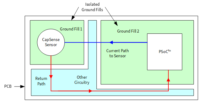
Figure 249. Proper current loop layout
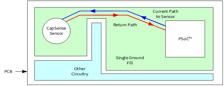
RF source location
If your system has a circuit that generates RF noise, such as a switched-mode power supply (SMPS) or an inverter, you should place these circuits away from the CAPSENSE™ interface. You should also shield such circuits to reduce the emitted RF.
Figure 250
shows an example of separating the RF noise source from the CAPSENSE™ interface.
Figure 250. Separating noise sources

Firmware considerations
The following parameters affect Radiated Emissions (RE) in a CAPSENSE™ system:
Device operating voltage
Device operation frequency
Sensor switching frequency
Shield signal
Sensor scan time
Sense Clock Source Inactive sensor termination
The following sections explain the effect of each parameter.
Device operating voltage
The emission is directly proportional to the voltage levels at which switching happens. Reducing the operating voltage helps to reduce the emissions as the amplitude of the switching signal at any output pin directly depends on the operating voltage of the device.
PSOC™ allows you to operate at lower operating voltages, thereby reducing the emissions.
Figure 251
and
Figure 252
show the impact of operating voltage on radiated emissions. Because IMO = 24 MHz, there is a spike at 24 MHz and the other spikes are caused by different hardware and firmware operations of the device.
Figure 251. Effect of V DD on radiated emissions (150 kHz – 30 MHz)
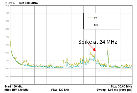
Figure 252. Effect of V DD on radiated emissions (30 MHz – 1 GHz)
Note: Frequency axis is in log scale.
Device operating frequency
Reducing the system clock frequency (IMO frequency) reduces radiated emissions. However, reducing the IMO frequency may not feasible in all applications because the IMO frequency impacts the CPU clock and all other system timings. Choose a suitable IMO frequency based on your application.
Sensor-switching frequency
Reducing the sensor-switching frequency (see
Sense clock
) also helps to reduce radiated emissions. See
Figure 253
and
Figure 254
. Because IMO = 24 MHz, there is a spike at 24 MHz and the other spikes are caused by different hardware and firmware operations of the device.
Figure 253. Effect of sensor-switching frequency on radiated emissions (150 kHz – 30 MHz)
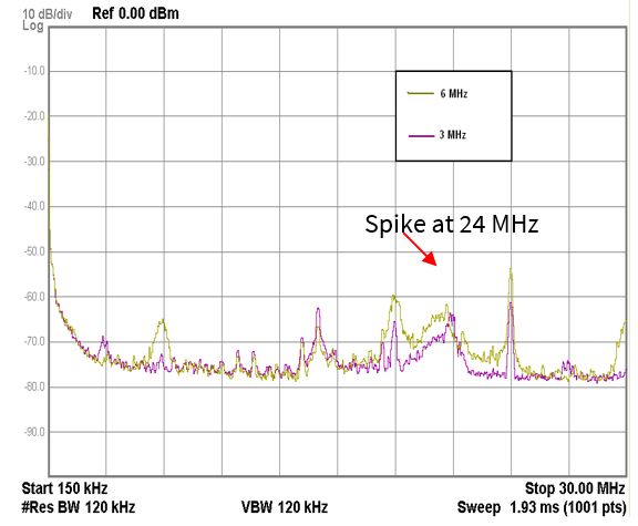
Figure 254. Effect of sensor-switching frequency on radiated emissions (30 MHz – 1 GHz)
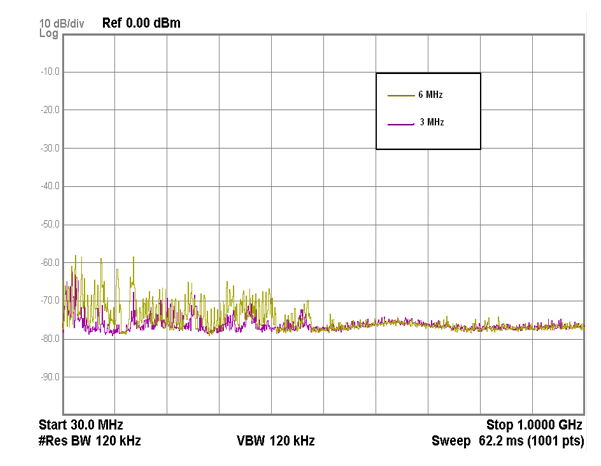
Note: Frequency axis is in log scale.
Pseudo random sense clock
The PSOC™ 4 device supports PRS-based sense clock generation. A PRS is used instead of a fixed clock source to attenuate emitted noise on the CAPSENSE™ pins by reducing the amount of EMI created by a fixed-frequency source and to increase EMI immunity from other sources and their harmonics.
Spread spectrum sense clock
In addition to the PRS-based clock generation, the PSOC™ 4 S-Series, PSOC™ 4100S Plus, PSOC™ 4100PS, and PSOC™ 6 MCU family of devices supports a unique feature called spread spectrum sense clock generation, in which the sense clock frequency is spread over a desired range. This method will help to reduce the peaks and spread out the emissions over a range of frequencies. The spread spectrum clock can be enabled by selecting the Sense Clock Source as SSCn. The range of frequency spread is decided by the length of the register. For more details on the spread spectrum clock generation in the PSOC™ 4 S-Series, PSOC™ 4100S Plus, and PSOC™ 4100PS family, see the Spread spectrum clock section in the CAPSENSE™ chapter of the respective device
Technical reference manual
.
Figure 255. Sense clock sources in PSOC™ 4 S-Series, PSOC™ 4100S Plus, and PSOC™ 4100PS family
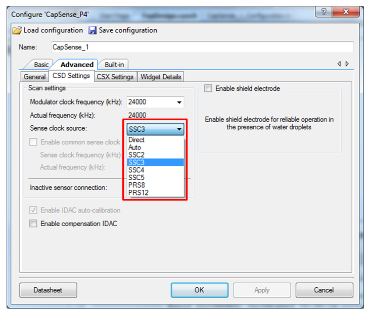
Shield signal
Shield signal
Enabling the shield signal (see
Driven shield signal and shield electrode
) on the hatch pattern increases the radiated emissions. Enable the driven-shield signal only for liquid-tolerant, proximity-sensing, or high-parasitic-capacitance designs. Also, if the shield must be used, ensure that the shield electrode area is limited to a width of 1 cm from the sensors, as
Figure 236
shows.
and
Figure 257
show the impact of enabling the driven-shield signal on the hatch pattern surrounding the sensors on radiated emissions.
Note: In these figures, the hatch pattern is grounded when the driven-shield signal is disabled. Because IMO = 24 MHz, there is a spike at 24 MHz and the other spikes are caused by different hardware and firmware operations of the device.
Figure 256. Effect of shield electrode on radiated emissions (150 kHz – 30 MHz)
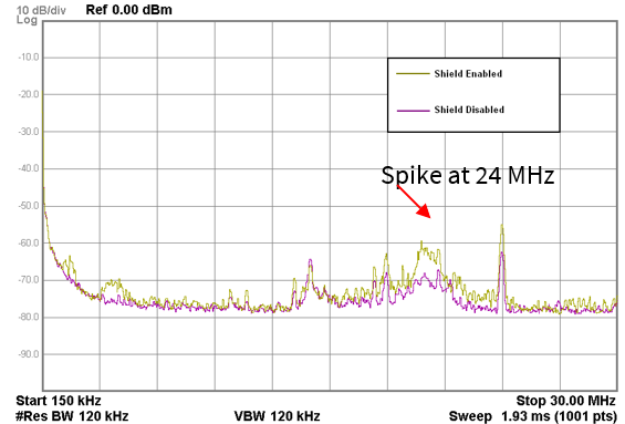
Figure 257. Effect of shield electrode on radiated emissions (30 MHz – 1 GHz)
Note: Frequency axis is in log scale.
Sensor scan time
Reducing the sensor scan time reduces the average radiated emissions. The sensor-scan time depends on the scan resolution and modulator clock divider (see
Figure 50
). Increasing the scan resolution or modulator clock divider increases the scan time.
and
Figure 259
show the impact of sensor scan time on radiated emissions. Note that, here, the sensor scan time was varied by changing the scan resolution. Because IMO = 24 MHz, there is a spike at 24 MHz and the other spikes are caused by different hardware and firmware operations of the device.
Parameter | Total scan time for five buttons | |
|---|---|---|
0.426 ms | 0.106 ms | |
Modulation clock divider | 2 | 2 |
Scan resolution | 10 bits | 8 bits |
Individual sensor scan time | 0.085 ms | 0.021 ms |
Figure 258. Effect of scan time on radiated emissions (150 kHz – 30 MHz)
Figure 259. Effect of scan time on radiated emissions (30 MHz – 1 GHz)
Note: Frequency axis is in log scale.
Sense clock source
Using PRS instead of direct clock drive as sense clock source spreads the radiated spectrum and hence reduces the average radiated emissions. See
Figure 260
and
Figure 261
. Because IMO = 24 MHz, there is a spike at 24 MHz and the other spikes are caused by different hardware and firmware operations of the device.
Figure 260. Effect of sense clock source on radiated emissions (150 kHz – 30 MHz)
Figure 261. Effect of sense clock source on radiated emissions (30 MHz – 1 GHz)
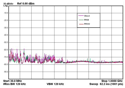
Note: Frequency axis is in log scale.
Inactive sensor termination
Connecting inactive sensors to ground reduces the radiated emission by a greater degree than connecting them to the shield.
Figure 262
and
Figure 263
show the impact of different inactive sensor terminations on radiated emission. Because IMO = 24 MHz, there is a spike at 24 MHz and the other spikes are caused by different hardware and firmware operations of the device.
Figure 262. Effect of inactive sensor termination on radiated emissions (150 kHz – 30 MHz)
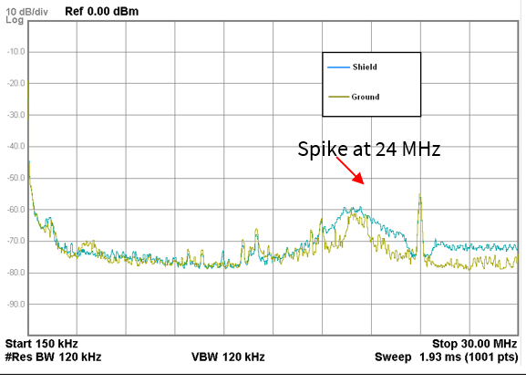
Figure 263. Effect of inactive sensor termination on radiated emissions (30 MHz – 1 GHz)
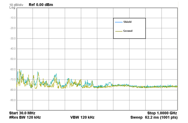
Note: Frequency axis is in log scale.
Conducted RF noise
The noise current that enters the CAPSENSE™ system through the power and communication lines is called conducted noise. You can use the following techniques to reduce the conducted RF noise.
Use decoupling capacitors on the power supply pins to reduce the conducted noise from the power supply. See section Power supply layout recommendations and the Device datasheet for details
Provide GND and VDD planes on the PCB to reduce current loops
If the PSOC™ PCB is connected to the power supply using a cable, minimize the cable length and consider using a shielded cable
To reduce high-frequency noise, place a ferrite bead around power supply or communication lines.
AMUX Splitter switch noise
Note: This section is specific to PSOC™ 4100S Max, and PSOC™ 4100T Plus devices.
For optimal performance of CAPSENSE™, it is recommended to use the pins directly connected to the same section of the AMUXBUS as the MSCLP block. This delivers better SNR compared to pins routed through the AMUXSPLITTER switches. Using directly connected pins, helps avoid the parasitic effect of the AMUXSPLITTER switches. Refer to
Table 48
, for recommended ports.
Device | Recommended ports |
|---|---|
PSOC™ 4100T Plus | 0, 1, 3, 4, 5, 6 |
PSOC™ 4100S Max | Channel 0: 3, 4, 6,10, 11, 12 Channel 1: 0, 5, 7, 8, 9 |
Refer
Figure 264
, which illustrates an example of a 4100T Plus device, where Port 2 pins are routed through the AMUX splitter switches.
Figure 264. Splitter switches
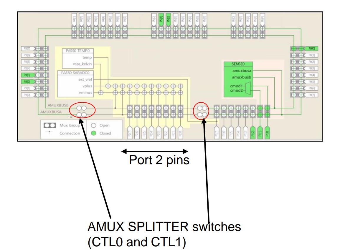
Effect of grounding
CSX method
The equivalent capacitances formed in the CSX method when a finger touches the CSX sensor is shown in
Figure 265
. From
Figure 265
, current drawn from the IDAC (IRX) has two components:
I
mt
and
I
sc
. These two components depend on the ratio of
C
bodyDG
/
C
fs
. Because the raw count depends on the amount of current drawn from IDAC, the increase and decrease of
C
bodyDG
/
C
fs
will affect the raw count of the sensor and cause a sudden change in the behavior on some conditions. To understand it better, consider two extreme conditions which cause
C
bodyDG
>>
C
fs
and
C
bodyDG
<<
C
fs
.
Figure 265. Equivalent circuit of the CSX sensor when finger is placed on the button
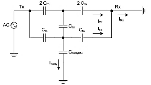
Where,
C M
= Mutual capacitance between the Rx and Tx electrode
C fs
= Capacitance formed between the surface of the finger and electrode
C fm
= Virtual capacitance which reduces the mutual-capacitance C
M
due to placing a finger
C bodyDG
= Body capacitance relative to the device ground
Figure 266. Current drawn from IDAC in CSX method
I mt
is due to the effective mutual-capacitance between the Tx and Rx electrode.
I sc
= Parasitic current that flows due to the capacitance formed between the sensor and finger
CbodyDG≫Cfs
Because
C
bodyDG
>>
C
fs
, you can replace
C
bodyDG
with a ground conductor; the resulting equivalent circuit appears as shown in
Figure 267
. Whenever there is a finger touch, the current drawn from the IDAC is directly dependent upon the effective mutual-capacitance between the Tx and Rx. This condition is observed in a good board design.
Figure 267. Equivalent circuit of the CSX sensor when CbodyDG >> Cfs
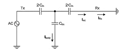
CbodyDG≪Cfs
This condition (
C
bodyDG
<<
C
fs
) is observed when a finger touches a CSX button with a very thin overlay or no overlay, or a finger touching the Rx and Tx electrodes directly, or a water drop being present on the Rx and Tx electrode only. Because
C
bodyDG
<<
C
fs
, you can remove
C
bodyDG
; the equivalent circuit for this case is as shown in
Figure 268
. In this condition, the capacitance introduced by the finger to the electrode
C
fs
is very high compared to the capacitance of the finger relative to the device ground
C
bodyDG
.
From
Figure 268
, it forms a balanced bridge circuit. Due to this, no current flows through
C
fm
, and also due to increase in
C
fs
,
I
sc
increases and thus additional current is drawn from the IDAC. This causes an unexpected behavior of decrease in the raw count.
Figure 268. Equivalent circuit of the CSX sensor when Cbody<<Cfs
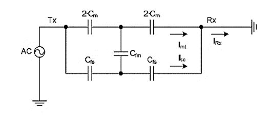
For CSX sensors, design should focus on increasing the ratio of CbodyDG / Cfs. Following are the examples for increasing the ratio of CbodyDG / Cfs:
CbodyDG/ Cfs ratio depends on the thickness of the overlay, size of the sensor, and many other factors. By experimental data, you are recommended not to use overlay thickness below 0.5 mm for CSX sensor. See
Overlay thickness
If the sensor is surrounded by hatch fill connected to ground, there is a lower chance that C bodyDG << Cfs. Therefore, ensure good ground in the design. Follow the best practices for the PCB layout guidelines described in this chapter
In the design, it is recommended to isolate the trace lines of Rx and Tx electrode, external capacitors, and resistors of the CSX touch sensing system from any conducting surface or a finger touch to avoid direct interaction. Not following this recommendation may cause CbodyDG<< Cfs
CSD method
The equivalent capacitances formed in the CSD method when a finger touches the CSD sensor is shown in
Figure 269
. It shows that the current drawn from the IDAC directly depends on the capacitance introduced by the finger touch.
I
CP
is a fixed component and
I
CF
depends on
C
F
,
C
BG
,
C
GE
. From
Sigma-delta converter
, the raw count depends on the amount of current drawn from IDAC. To understand it better, consider two scenarios of an AC/ DC mains-powered application and a battery-powered application.
Figure 269. Equivalent circuit of the CSD sensor
Figure 270. Current drawn from IDAC in CSD method
AC/DC-powered application
In an AC / DC-powered application using the mains supply, device ground is strongly coupled to earth ground. Thus, you can replace
C
GE
with a conductor and C
BG
is usually 100 pF to 200 pF. Since
C
BG
is large when compared to
C
F
, you can neglect its effect. Finally, the resulting equivalent circuit is shown in
Figure 271
. The increase in total capacitance draws a higher current from the IDAC achieving a higher change in raw count for a finger touch. Thus, in this condition, you get a higher sensitivity, which means that you will get a higher signal for a finger touch.
Figure 271. Equivalent circuit of the CSD sensor for mains-powered application
Battery-powered application
In battery-powered portable applications, device ground and earth ground are lightly coupled, thus
C
GE
is small. The resulting equivalent circuit is shown in
Figure 272
. Thus, in this condition, you get a lower sensitivity; that means you will get a lower signal for a finger touch, which is due to a decrease in capacitance seen at the device.
Figure 272. Equivalent circuit of the CSD for battery-powered application
Following are the recommendations for a CSD system design in a portable application powered by a battery:
Add a large ground plane to the system. The ground plane should be away from the sensing element such that it does not increase the parasitic capacitance of the sensor. Follow the best practices for the PCB layout guidelines described in this chapter
Use a driven shield to improve the sensitivity of portable devices. Refer to the Layout guidelines for shield electrode for more details
Reduce the thickness of the overlay material or use an overlay with better dielectric value to improve sensitivity
Tune the CAPSENSE™ system with powering it by a battery source
CAPSENSE™ Plus
PSOC™ 4 can perform many additional functions along with CAPSENSE™. The wide variety of features offered by this device allows you to integrate various system functions in a single chip, as
Figure 273
shows. Such applications are known as CAPSENSE™ Plus applications.
Figure 273. CAPSENSE™ Plus
The additional features available in a PSOC™ 4 device include:
Communication: Bluetooth® LE, I 2 C, UART, SPI, CAN, and LIN
Analog functions: ADC, comparators, and opamps
Digital functions: PWMs, counters, timers, and UDBs
Segment LCD drive
Bootloaders
Different power modes: Active, sleep, deep sleep, hibernate, and stop
While using above mentioned additional features, it is recommended to configure it in sinking mode as applicable.
For more information on PSOC™ 4, see AN79953 - Getting started with PSOC™ 4 , or AN91267 - Getting started with PSOC™ 4 Bluetooth® LE.
The flexibility of the PSOC™ 4 and the unique PSOC™ Creator IDE allow you to quickly make changes to your design, which accelerates time-to-market. Integrating other system functions significantly reduces overall system cost. Table 49 shows a list of example applications, where using CAPSENSE™ Plus can result in significant cost savings.
Application | CAPSENSE™ | Opamp | ADC | Comp | PWM, Counter, Timer, UDBs | Comm(Bluetooth® LE, I2C, SPI, UART) | LCD drive | GPIOs |
|---|---|---|---|---|---|---|---|---|
Heart rate monitor (wrist band) | User interface: buttons, linear sliders | TIA, Buffer | Heart Rate Measurement, Battery voltage measurement | LED Driving | Bluetooth® LE | Segment LCD | LED indication | |
LED bulb | User interface: buttons, radial sliders | Amplifier | LED current measurement | Short circuit protection | LED color control (PrISM*) | Bluetooth® LE | LED indication | |
Washing machine | User interface: buttons, radial sliders | Temperature sensor | Water level monitor | Buzzer, FOC** motor control | I2 C LCD display, UART network interface | Segment LCD | LED indication | |
Water heater | User interface: buttons, linear sliders | Temperature sensor, water flux sensor | Water level monitor | Buzzer | I2 C LCD display, UART Network Interface | Segment LCD | LED indication | |
IR remote controllers | User interface: buttons, linear and radial sliders, touchpads | Manchester encoder | LED indication | |||||
Induction cookers | User interface: buttons, linear sliders | Temperature sensor | Segment LCD | LED indication | ||||
Motor control systems | User interface: buttons, linear sliders | BLDC*** and FOC motor control | LED indication | |||||
Gaming/simulation controllers | User interface: buttons, touchpads | Reading analog joysticks | I2 C/SPI/UART communication interface | Segment LCD | LED indication | |||
Thermal printers | User interface: buttons | Overheat protection, paper sensor | Stepper motor control | SPI communication interface | LED indication |
- PrISM = Precision illumination signal modulation
** FOC = Field oriented control
*** BLDC = Brushless DC motor
shows a general block diagram of a CAPSENSE™ Plus application, such as an induction cooker or a microwave oven.
Figure 274. CAPSENSE™ Plus system with PSOC™ 4
In this application, the 12-bit 1 Msps SAR ADC in the PSOC™ 4 detects over-current, overvoltage, and high temperature conditions. The PWM output drives the speaker for status and alarm tones. Another PWM controls the heating element in the system. The CAPSENSE™ buttons and slider constitute the user interface. PSOC™ 4 can also drive a segment LCD for visual outputs. PSOC™ 4 has a serial communication block that can connect to the main board of the system.
shows the application-level block diagram of a fitness tracker based on PSOC™ 6 MCU with Bluetooth® LE Connectivity. The device provides a one-chip solution and includes features like activity monitoring, environment monitoring, CAPSENSE™ for user interface, Bluetooth® LE connectivity, and so on. For more information on PSOC™ 6 MCU, see
AN210781 – Getting started with PSOC™ 6 MCU with Bluetooth® LE connectivity
.
Figure 275. Fitness tracker application with PSOC™ 6 MCU with Bluetooth® LE connectivity block diagram
Resources
Website
Visit the
Getting started with PSOC™ 4
,
Getting started with PSOC™ 4 Bluetooth® LE
,
Getting started with PSOC™ 6 MCU
, and
Getting started with PSOC™ 6 MCU with Bluetooth® LE connectivity
website to understand the PSOC™ 4, PSOC™ 6 MCU with Bluetooth® LE connectivity.
Device datasheet
Component datasheet/middleware document
Technical reference manual
The
PSOC™ 4 Technical reference manual (TRM)
and
PSOC™ 6 Technical reference manual (TRM)
provide quick and easy access to information on PSOC™ 4 and PSOC™ 6 architecture including top-level architectural diagrams, register summaries, and timing diagrams.
Development kits
lists Infineon® development kits that support PSOC™ 4 and PSOC™ 6 CAPSENSE™.
PSOC™ Creator
PSOC™ Creator is a state-of-the-art, easy-to-use integrated development environment. See the
PSOC™ Creator home page
.
ModusToolbox™
ModusToolbox™ software suite is used for the development of PSOC™ 4 and PSOC™ 6 based CAPSENSE™ applications. You can download the ModusToolbox™ software
here
. The related documents are as follows:
ModusToolbox™ release notes
ModusToolbox™ install guide
ModusToolbox™ user guide
ModusToolbox™ quick start guide
ModusToolbox™ software training
ModusToolbox™ CAPSENSE™ configurator
ModusToolbox™ CAPSENSE™ tuner
ModusToolbox™ device configurator
ModusToolbox™ SmartIO configurator
PSOC™ Creator to ModusToolbox™
ModusToolbox™ command line
Application notes and design guides
® A large collection of application notes are available to get your design up and running fast. See
PSOC™ 4 application notes
,
PSOC™ 4 Bluetooth® LE application notes
,
CAPSENSE™ application notes and design guides
.
Following is the list of CAPSENSE™ specific applications notes:
Design guide for PSOC™ 3 and PSOC™ 5LP devices
Design guides for the CAPSENSE™ Express family
CY8CMBR3XXX CAPSENSE™ design guide
CY8CMBR2110 CAPSENSE™ design guide
CY8CMBR2016 CAPSENSE™ design guide
CY8CMBR2010 CAPSENSE™ design guide
CY8CMBR2044 CAPSENSE™ design guide
CAPSENSE™ Express™: CY8C201XX application notes
Design guides for PSOC™ 1 devices
CY8C20XX7/S design guide
CY8C20XX6A/H CAPSENSE™ design guide
CY8C21X34/B CAPSENSE™ design guide
CY8C20X34 CAPSENSE™ design guide
Getting started application note
Design support
Knowledge base articles – Browse technical articles by product family or perform a search on CAPSENSE™ topics
White papers – Learn about advanced capacitive-touch interface topics
Infineon developer community – Connect with the technical community and exchange information
Video library – Quickly get up to speed with tutorial videos
Quality and reliability – We are committed to complete customer satisfaction. At our Quality website, you can find reliability and product qualification reports
- https://www.infineon.com/cms/en/about-infineon/company/contacts/support/
– Submit your design for review by creating a support case. You need to register and login at the website to be able to contact technical support . It is recommended to use PDF prints for the schematic and Gerber files with layer information for the layout
AMUXBUS
Analog multiplexer bus available inside PSOC™ that helps to connect I/O pins with multiple internal analog signals.
Baseline
A value resulting from a firmware algorithm that estimates a trend in the Raw Count when there is no human finger present on the sensor. The Baseline is less sensitive to sudden changes in the Raw Count and provides a reference point for computing the Difference Count.
Button or button widget
A widget with an associated sensor that can report the active or inactive state (that is, only two states) of the sensor. For example, it can detect the touch or no-touch state of a finger on the sensor.
Difference count
The difference between Raw Count and Baseline. If the difference is negative, or if it is below Noise Threshold, the Difference Count is always set to zero.
Capacitive sensor
A conductor and substrate, such as a copper button on a printed circuit board (PCB), which reacts to a touch or an approaching object with a change in capacitance.
CAPSENSE™
Infineon® Touch-sensing user interface solution. The industry’s No. 1 solution in sales by 4x over No. 2.
CAPSENSE™ Mechanical Button Replacement (MBR)
Configurable solution to upgrade mechanical buttons to capacitive buttons, requires minimal engineering effort to configure the sensor parameters and does not require firmware development. These devices include the CY8CMBR3XXX and CY8CMBR2XXX families.
CAPSENSE™ Mechanical Button Replacement (MBR)
Centroid or Centroid Position
A number indicating the finger position on a slider within the range given by the Slider Resolution. This number is calculated by the CAPSENSE™ centroid calculation algorithm.
Compensation IDAC
A programmable constant current source, which is used by CSD to compensate for excess sensor C P . This IDAC is not controlled by the Sigma-Delta Modulator in the CSD block unlike the Modulation IDAC.
CAPSENSE™ Sigma Delta
CAPSENSE™ Sigma Delta (CSD) is a patented method of performing self-capacitance (also called self-cap) measurements for capacitive sensing applications.
In CSD mode, the sensing system measures the self-capacitance of an electrode, and a change in the self-capacitance is detected to identify the presence or absence of a finger.
CSD
Debounce
A parameter that defines the number of consecutive scan samples for which the touch should be present for it to become valid. This parameter helps to reject spurious touch signals.
A finger touch is reported only if the Difference Count is greater than Finger Threshold + Hysteresis for a consecutive Debounce number of scan samples.
Driven-shield
A technique used by CSD for enabling liquid tolerance in which the Shield Electrode is driven by a signal that is equal to the sensor switching signal in phase and amplitude.
Electrode
A conductive material such as a pad or a layer on PCB, ITO, or FPCB. The electrode is connected to a port pin on a CAPSENSE™ device and is used as a CAPSENSE™ sensor or to drive specific signals associated with CAPSENSE™ functionality.
Finger threshold
A parameter used with Hysteresis to determine the state of the sensor. Sensor state is reported ON if the Difference Count is higher than Finger Threshold + Hysteresis, and it is reported OFF if the Difference Count is below Finger Threshold – Hysteresis.
Ganged sensors
The method of connecting multiple sensors together and scanning them as a single sensor. Used for increasing the sensor area for proximity sensing and to reduce power consumption.
To reduce power when the system is in low-power mode, all the sensors can be ganged together and scanned as a single sensor taking less time instead of scanning all the sensors individually. When you touch any of the sensors, the system can transition into active mode where it scans all the sensors individually to detect which sensor is activated.
PSOC™ supports sensor-ganging in firmware, that is, multiple sensors can be connected simultaneously to AMUXBUS for scanning.
Gesture
Gesture is an action, such as swiping and pinch-zoom, performed by the user. CAPSENSE™ has a gesture detection feature that identifies the different gestures based on predefined touch patterns. In the CAPSENSE™ Component, the Gesture feature is supported only by the Touchpad Widget.
Guard sensor
Copper trace that surrounds all the sensors on the PCB, similar to a button sensor and is used to detect a liquid stream. When the Guard Sensor is triggered, firmware can disable scanning of all other sensors to prevent false touches.
Hatch fill or hatch ground or hatched ground
While designing a PCB for capacitive sensing, a grounded copper plane should be placed surrounding the sensors for good noise immunity. But a solid ground increases the parasitic capacitance of the sensor which is not desired. Therefore, the ground should be filled in a special hatch pattern. A hatch pattern has closely-placed, crisscrossed lines looking like a mesh and the line width and the spacing between two lines determine the fill percentage. In case of liquid tolerance, this hatch fill referred as a shield electrode is driven with a shield signal instead of ground.
Hysteresis
A parameter used to prevent the sensor status output from random toggling due to system noise, used in conjunction with the Finger Threshold to determine the sensor state.
IDAC (current-output digital-to-analog converter)
Programmable constant current source available inside PSOC™, used for CAPSENSE™ and ADC operations.
current-output digital-to-analog converter
Liquid tolerance
The ability of a capacitive sensing system to work reliably in the presence of liquid droplets, streaming liquids or mist.
Linear slider
A widget consisting of more than one sensor arranged in a specific linear fashion to detect the physical position (in single axis) of a finger.
Low baseline reset
A parameter that represents the maximum number of scan samples where the Raw Count is abnormally below the Negative Noise Threshold. If the Low Baseline Reset value is exceeded, the Baseline is reset to the current Raw Count.
Manual-tuning
The manual process of setting (or tuning) the CAPSENSE™ parameters.
Matrix buttons
A widget consisting of more than two sensors arranged in a matrix fashion, used to detect the presence or absence of a human finger (a touch) on the intersections of vertically and horizontally arranged sensors.
If M is the number of sensors on the horizontal axis and N is the number of sensors on the vertical axis, the Matrix Buttons Widget can monitor a total of M x N intersections using ONLY M + N port pins.
When using the CSD sensing method (self-capacitance), this Widget can detect a valid touch on only one intersection position at a time.
Modulation capacitor (CMOD)
An external capacitor required for the operation of a CSD block in Self-Capacitance sensing mode.
Modulator clock
A clock source that is used to sample the modulator output from a CSD block during a sensor scan. This clock is also fed to the Raw Count counter. The scan time (excluding pre and post processing times) is given by (2 N – 1)/Modulator Clock Frequency, where N is the Scan Resolution.
Modulation IDAC
Modulation IDAC is a programmable constant current source, whose output is controlled (ON/OFF) by the sigma-delta modulator output in a CSD block to maintain the AMUXBUS voltage at V REF . The average current supplied by this IDAC is equal to the average current drawn out by the sensor capacitor.
Multi sense converter (MSC)
The multi sense converter is the analog to digital converter used in Fifth-Generation CAPSENSE™ technology also known as Ratiometric sensing technology.
Mutual-capacitance
Capacitance associated with an electrode (say Tx) with respect to another electrode (say Rx) is known as mutual-capacitance.
Negative noise threshold
A threshold used to differentiate usual noise from the spurious signals appearing in negative direction. This parameter is used in conjunction with the Low Baseline Reset parameter.
Baseline is updated to track the change in the Raw Count as long as the Raw Count stays within Negative Noise Threshold, that is, the difference between Baseline and Raw count (Baseline – Raw count) is less than Negative Noise Threshold.
Scenarios that may trigger such spurious signals in a negative direction include: a finger on the sensor on power-up, removal of a metal object placed near the sensor, removing a liquid-tolerant CAPSENSE™-enabled product from the water; and other sudden environmental changes.
CAPSENSE™ noise (Noise)
The variation in the Raw Count when a sensor is in the OFF state (no touch), measured as peak-to-peak counts.
CAPSENSE™ noise (Noise)
Noise threshold
A parameter used to differentiate signal from noise for a sensor. If Raw Count – Baseline is greater than Noise Threshold, it indicates a likely valid signal. If the difference is less than Noise Threshold, Raw Count contains nothing but noise.
Noise threshold
Overlay
A non-conductive material, such as plastic and glass, which covers the capacitive sensors and acts as a touch-surface. The PCB with the sensors is directly placed under the overlay or is connected through springs. The casing for a product often becomes the overlay.
Parasitic capacitance (CP)
Parasitic capacitance is the intrinsic capacitance of the sensor electrode contributed by PCB trace, sensor pad, vias, and air gap. It is unwanted because it reduces the sensitivity of CSD.
Proximity sensor
A sensor that can detect the presence of nearby objects without any physical contact.
Proximity sensor
Radial slider
A widget consisting of more than one sensor arranged in a specific circular fashion to detect the physical position of a finger.
Radial slider
Raw count
The unprocessed digital count output of the CAPSENSE™ hardware block that represents the physical capacitance of the sensor.
Refresh interval
The time between two consecutive scans of a sensor.
Scan resolution
Resolution (in bits) of the Raw Count produced by the CSD block.
Scan time
Time taken for completing the scan of a sensor.
Self-capacitance
The capacitance associated with an electrode with respect to circuit ground.
Sensitivity
The change in Raw Count corresponding to the change in sensor capacitance, expressed in counts/pF. Sensitivity of a sensor is dependent on the board layout, overlay properties, sensing method, and tuning parameters.
Sense clock
A clock source used to implement a switched-capacitor front-end for the CSD sensing method.
Sensor
See Capacitive sensor.
Sensor auto reset
A setting to prevent a sensor from reporting false touch status indefinitely due to system failure, or when a metal object is continuously present near the sensor.
When Sensor Auto Reset is enabled, the Baseline is always updated even if the Difference Count is greater than the Noise Threshold. This prevents the sensor from reporting the ON status for an indefinite period of time. When Sensor Auto Reset is disabled, the Baseline is updated only when the Difference Count is less than the Noise Threshold.
Sensor ganging
See Ganged sensors.
Shield electrode
Copper fill around sensors to prevent false touches due to the presence of water or other liquids. Shield Electrode is driven by the shield signal output from the CSD block. See Driven-shield .
Shield tank capacitor
An optional external capacitor (C SH Tank Capacitor) used to enhance the drive capability of the CSD shield, when there is a large shield layer with high parasitic capacitance.
signal (CAPSENSE™ signal)
Difference Count is also called Signal. See Difference Count.
Signal-to-noise ratio
The ratio of the sensor signal, when touched, to the noise signal of an untouched sensor.
Slider resolution
A parameter indicating the total number of finger positions to be resolved on a slider.
SmartSense™ auto-tuning
A CAPSENSE™ algorithm that automatically sets sensing parameters for optimal performance after the design phase and continuously compensates for system, manufacturing, and environmental changes.
Touchpad
A Widget consisting of multiple sensors arranged in a specific horizontal and vertical fashion to detect the X and Y position of a touch.
Trackpad
See Touchpad.
Tuning
The process of finding the optimum values for various hardware and software or threshold parameters required for CAPSENSE™ operation.
VREF
Programmable reference voltage block available inside PSOC™ used for CAPSENSE™ and ADC operation.
Widget
A user-interface element in the CAPSENSE™ Component that consists of one sensor or a group of similar sensors. Button, proximity sensor, linear slider, radial slider, matrix buttons, and touchpad are the supported widgets.
Revision history
Document version | Date of release | Description of changes |
|---|---|---|
2013-04-19 | ** | New Design Guide. |
2013-07-29 | *A | Added dual IDAC support. Updated some schematics in chapter 6. Other minor changes to chapters 3, 5, and 6. |
2013-11-13 | *B | Added support of CY8C4000 devices. Minor fixes throughout the document. |
2014-02-24 | *C | Updated the table of device features. Changed IDAC names to sync with new PSOC™ Creator Component terms. Added a schematic checklist. Changed screenshots to match the new Component version. |
2014-02-27 | *D | Updated Table 1-1 per PSOC™ 4000 datasheet. |
2014-03-20 | *E | Added firmware design considerations to Chapter 6. Added power supply layout and schematic considerations to Chapter 6. Updated the IMO range for PSOC™ 4000 |
2014-04-15 | *F | Updated to support PSOC™ 4000 and PSOC™ Creator 3.0 SP1. |
2014-08-29 | *G | Added Reference to Getting started with CAPSENSE™ in Proximity (three-dimensional) Renamed Liquid tolerance to Liquid tolerance and re-wrote this section. Updated the recommendations for Shield drive that is Csh_tank precharge and CMOD precharge in CAPSENSE™ CSD shielding CAPSENSE™ CSD shielding. Added recommendation for setting “API resolution” in Chapter Added guidelines on how to select value of “Sensitivity” parameter in Chapter Updated recommended values of threshold and hysteresis parameters in Chapter Manual tuning trade-offs Added Section Manual Tuning Slider Example. Updated maximum overlay thickness value for sliders in Table 32. Added guideline on maximum thickness for overlays of materials other than acrylic in Overlay thickness Overlay thickness. Re-wrote Chapter Slider design. Added recommendations on DC loads in Sensor and device placement Renamed and rewrote Layout guidelines for liquid tolerance to Layout guidelines for liquid tolerance. Added External capacitors pin selection External capacitors pin selection. Updated slider related recommendations in Layout rule Updated Electromagnetic compatibility (EMC) considerations , added extensive data on hardware and firmware considerations. |
2014-12-19 | *H | Added information for the PSOC™ 4 Bluetooth® LE family of devices. Added information for the PRoC Bluetooth® LE family of devices. Updated ground and power layout guidelines in Ground plane and Power supply layout recommendations. |
2015-01-21 | *I | Added information for PSOC™ 4200-M family of devices. Added footnote in chapter Slider. Added GPIO source/sink current limit in Table 39. Changed document title to PSOC™ 4 CAPSENSE™ Design Guide – AN85951 |
2015-06-02 | *J | Changed Document Title to “AN85951 – PSOC™ 4 CAPSENSE™ Design Guide” . Updated Design considerations Updated Preventing ESD discharge. Updated Figure 244. Updated Redirect. Replaced "Guard Ring" with "Ground Ring". |
2015-08-20 | *K | Added Table 3-1. Removed chapter 3.2.1 C MOD Precharge. Added chapter CAPSENSE™ in PSOC™ 4xxxM/4xxxL-Series. Updated chapter Trace routing. Added reference of AN2397. Added recommendation for modulator clock divider in chapter Manual tuning trade-offs. Added Figure 241 |
2015-09-16 | *L | Updated Overview . Updated Figure 1 Figure 1. |
2016-01-19 | *M | Updated Introduction . Updated Chapters PSOC™ 4 and PSOC™ 6 MCU and for CAPSENSE™ performance details. Added section to CAPSENSE™ design and development tools. Added Glossary. |
2016-02-23 | *N | Added information on mutual-capacitance sensing in PSOC™ 4 device series. Added information on CAPSENSE™ 3.0 changes. Added following sections: Updated following sections: |
2016-03-04 | *O | Added PSOC™ Analog Coprocessor references. Updated External capacitors pin selection . Updated Development kits chapter. Updated document title. Updated Copyright notice. |
2016-06-14 | *P | Updated IDAC sinking mode recommendation. Updated template. |
2016-11-18 | *Q | |
2017-04-19 | *R | Updated logo and copyright. |
2017-09-22 | *S | Added references to PSOC™ 4100S Plus throughout the document. Updated CAPSENSE™ features CAPSENSE™ features with PSOC™ 4100S Plus features. Updated PSOC™ 4 and PSOC™ 6 CAPSENSE™ development kits with CY8CKIT-149 PSOC™ 4100S Plus prototyping kit. Updated Application notes and design guides Application notes and design guides with specific list of CAPSENSE™ Application Notes |
2018-01-18 | *T | Changed document title Added references to PSOC™ 6 MCU features throughout the document Updated CAPSENSE™ generations in PSOC™ 4 and PSOC™ 6 CAPSENSE™ generations in PSOC™ 4 and PSOC™ 6 with generalized architecture block diagram for CSD sensing. Added Gesture in CAPSENSE™ Gesture in CAPSENSE™ . |
2018-02-28 | *U | Added references to PSOC™ 4100PS throughout the document. |
2018-11-08 | *V | Updated the entire document with references to CY8C62x8 and CY8C62xA devices. Updated the entire document with references to ModusToolbox™. Updated Table 9 with the information of PSOC™ 6 kits. Updated chapter Mutual-capacitance button design with the information of additional mutual cap key. Removed all references to PRoC Bluetooth® LE devices. |
2019-04-11 | *W | Updated SmartSense and Manual tuning with respect to the latest component. Removed details on different shield drive mode from CAPSENSE™ CSD Updated CAPSENSE™ CSX sensing
Removed a table in External capacitors pin selection chapter Updated Table 3 |
2020-01-07 | *X | Added Liquid tolerance for Mutual Capacitance Sensing section Removed Mutual Capacitance Button Design section Updated Table 3-2 and Table 3-3 Updated CAPSENSE™ CSX Sensing Method Added ModusToolBox™ section in Chapter 4 Updated SmartSense and Manual Tuning section with respect to the latest component. Updated Slider Tuning Guidelines section Added Tuning Shield Electrode section Updated Gesture chapter with gesture tuning guidelines Updated the Low Power design section Updated Sensor and Device placement section Updated Slider Design section Added Effect of Grounding in CSX method and Effect of Grounding in CSD method section |
2020-03-18 | *Y | Updated Sensor pin selection and chapters. |
2020-10-08 | *Z | Added CAPSENSE™ configurator CAPSENSE™ configurator. Moved Tuning Shield Electrode section under CSD sensing method (third- and fourth-generation) CSD sensing method (third- and fourth-generation). Added I am observing a low CM for my CSX button I am observing a low CM for my CSX button . Added Mutual-capacitance button design Mutual-capacitance button design . Added additional layout guidelines in Sensor and device placement Sensor and device placement . Added additional trace routing guidelines in Trace routing Trace routing . Added additional guard trace guidelines in Crosstalk Crosstalk . Added a single line description on self cap buttons in Self-capacitance button Self-capacitance button . Moved ESD and Electromagnetic compatibility (EMC) considerations under External noise External noise . Moved Effect of grounding on CSX method and effect of grounding on CSD method under Effect of grounding . |
2021-10-01 | AA | Updated to IFX template. Updated CAPSENSE™ features with new Fifth-Generation CAPSENSE™ block and PSOC™ 4100S Max features. Update Table 2. Added new section CAPSENSE™ CSD-RM sensing method (fifth-generation) and CAPSENSE™ CSX-RM sensing method (fifth-generation) . Added new section for features Autonomous scanning and Usage of multiple channels . Removed “5.3.2.4 Button widget example” and replaced with Button widget tuning . Added new chapter 5.3.2.6 "Touchpad widget tuning". Added new section for Fifth-generation CAPSENSE™ sensing method - CSD-RM sensing method (fifth-generation and fifth-generation low-power) and CSX-RM sensing method (fifth-generation and fifth-generation low-power) . Updated Table 32 , Table 40 , and Table 41 . Updated Copyright information. |
2022-07-21 | AB | Template update |
2022-12-20 | AC | In the Table 2 , in the Feature column, updated "Noise floor (pk-pk)" to "Noise floor (rms)". |
2023-08-04 | AD | Updated link references Deleted CSD Finger Detection Criteria Deleted CSX Finger Detection Criteria Added Synchronized scanning section Added CIC2 section Added the section title Advantages of fifth generation and fifth generation low-power |
2023-09-27 | AE |
|
2024-02-08 | AF | Fixed broken links. Removed "5.3.2.6 Touchpad widget tuning". Removed "5.3.3.5 Touchpad widget tuning". Removed "5.3.5.7 Touchpad widget tuning". |
2024-03-20 | AG | Information about CIC2 is updated in Chapter 3 . Updated measuring method for sense clock divider and added information about Cfine and CDAC configuration in Chapter 5 . Updated LDO recommendation information in Recommendations to reduce the VDDA noise section. |
2025-04-04 | AH | Information about MPSC-D is added in PSOC™ 4 and PSOC™ 6 MCU CAPSENSE™. Updated overlay recommendation information in Overlay selection . Updated recommendation for AMUX Splitter switch noise in Noise in CAPSENSE™ system . Updated MPSC-D (Multi-phase self-cap differential) , Advantages , Limitations of MPSC-D , and Implementation of MPSC-D . Added Capacitive DACs scaling . Updated Table 9 and Table 39 . |
Trademarks
The Bluetooth® word mark and logos are registered trademarks owned by Bluetooth SIG, Inc., and any use of such marks by Infineon is under license.
PSOC™, formerly known as PSoC™, is a trademark of Infineon Technologies. Any references to PSoC™ in this document or others shall be deemed to refer to PSOC™.
1 To achieve the best CAPSENSE™ performance, follow the recommendations in the Sensor pin selection section
3 VDDD is the device power supply for digital section.
4 The hardware state machine is a logic which controls the CAPSENSE™ block and sensor scanning.
5 Supports limited number of inputs. Refer to the device datasheet for more details.
6 When the decimation rate reaches its maximum of 255, the user needs to ensure that the below conditions are met to avoid the CIC2 accumulator (25-bit) overflow.
For Direct clock: (2
25
-1) >= TRUNC((Nsub*Sns_Clk_Div)/Decimation-1)*Decimation 2
For PRS clock: (2 25 -1)/2 >= TRUNC((Nsub*Sns_Clk_Div)/Decimation-1)*Decimation 2
7 CapSense_ADC is not supported in devices with fifth-generation CAPSENSE™ block.
9 CapSense_ADC is not supported in devices with the fifth-generation CAPSENSE™ block.
10 Here, a valid signal means that the difference count of the given slider segment is greater than or equal to the noise threshold value.
11 For a 5 mm acrylic overlay, the SmartSense Component requires a minimum of 9 mm finger diameter for slider operation. If the finger diameter is less than 9 mm, Manual Tuning should be used.
12 The recommended slider-segment width is based on an average human finger diameter of 9 mm. See section Slider-segment shape, width, and Air gap for more details.
13 The minimum slider segment height of 7 mm is recommended based on a minimum human finger diameter of 7 mm. Slider height may be kept lower than 7 mm if the overlay thickness and CAPSENSE™ tuning is such that an Signal-to-noise ratio (SNR) (SNR) ≥ 5:1 is achieved when the finger is placed in the middle of any segment.
14 Here, a valid signal means that the difference count of the given slider segment is greater than or equal to the noise threshold value.
15 The CAPSENSE™ Component in PSOC™ Creator reports a centroid of 0xFFFF when there is no finger detected on the slider, or when none of the slider segments reports a difference count value greater than the Finger Threshold parameter.
16 The CAPSENSE™ middleware in ModusToolbox™ reports a centroid of 0x0000 when there is no finger detected on the slider, or when none of the slider segments reports a difference count value greater than the Finger Threshold parameter.
17 The V DDA pin on PSOC™ 4 S-Series, PSOC™ 4100S Plus, and PSOC™ 4100PS family requires different values of bulk capacitor depending on the power supply source. If the device is battery powered, it is recommended to use 0.1 µF and 1 µF capacitors in parallel and if the device is mains powered, it is recommended to use 0.1 µF and 10 µF in parallel. This is to improve the power supply rejection ratio of reference generator (REFGEN) used in the CAPSENSE™ block.
18 These external capacitors are only used in the case of third- and fourth-generation CAPSENSE™
19 These external capacitors are only used in the case of third- and fourth-generation CAPSENSE™
20 Supported pin paring for PSOC™ 4100S Max: CMOD1/CMOD2 = P4[0] /P4[1] or P4[2] /P4[3] or P7[0] /P7[1] or P5[1] /P5[2]